14_oversampling_johns & martin slides
DESCRIPTION
Johns & Martin SlidesTRANSCRIPT
slide 1 of 56University of Toronto© D.A. Johns, K. Martin, 1997
Oversampling Converters
David Johns and Ken MartinUniversity of Toronto
slide 2 of 56University of Toronto© D.A. Johns, K. Martin, 1997
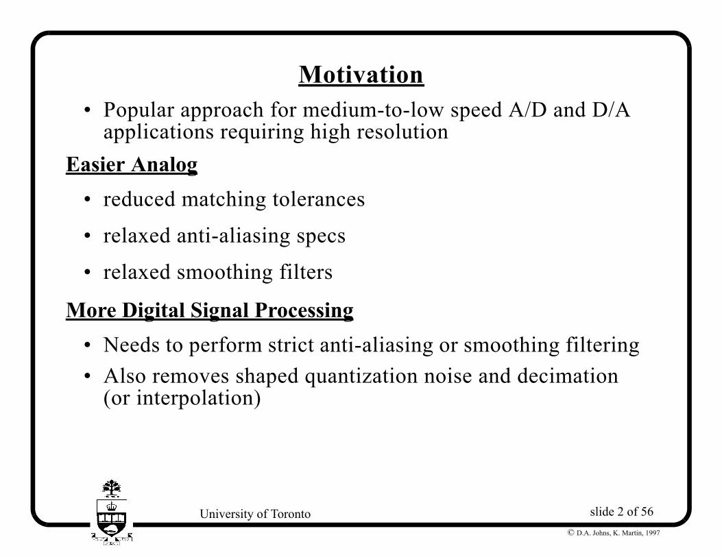
Motivation • Popular approach for medium-to-low speed A/D and D/A
applications requiring high resolutionEasier Analog
• reduced matching tolerances
• relaxed anti-aliasing specs
• relaxed smoothing filters
More Digital Signal Processing • Needs to perform strict anti-aliasing or smoothing filtering • Also removes shaped quantization noise and decimation
(or interpolation)
slide 3 of 56University of Toronto© D.A. Johns, K. Martin, 1997
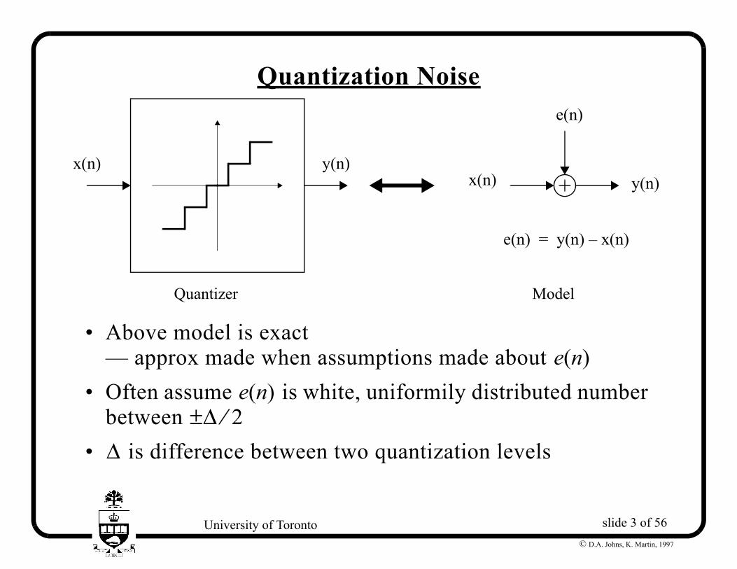
Quantization Noise
• Above model is exact— approx made when assumptions made about
• Often assume is white, uniformily distributed number between
• is difference between two quantization levels
x n( ) y n( )y n( )x n( )
e n( )
Quantizer Model
e n( ) y n( ) x n( )–=
e n( )e n( )
∆ 2⁄±∆
slide 4 of 56University of Toronto© D.A. Johns, K. Martin, 1997
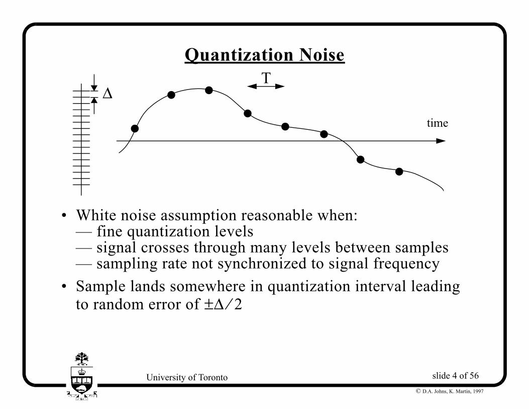
Quantization Noise
• White noise assumption reasonable when:— fine quantization levels— signal crosses through many levels between samples— sampling rate not synchronized to signal frequency
• Sample lands somewhere in quantization interval leading to random error of
∆
time
T
∆ 2⁄±
slide 5 of 56University of Toronto© D.A. Johns, K. Martin, 1997
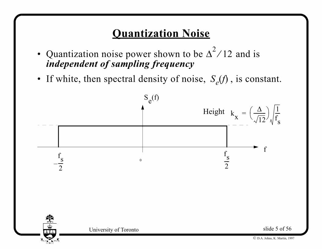
Quantization Noise
• Quantization noise power shown to be and is independent of sampling frequency
• If white, then spectral density of noise, , is constant.
∆2 12⁄
Se f( )
0fs2----
Se f( )
ffs2----–
kx∆12
---------- 1
fs----=Height
slide 6 of 56University of Toronto© D.A. Johns, K. Martin, 1997
Oversampling Advantage • Oversampling occurs when signal of interest is
bandlimited to but we sample higher than
• Define oversampling-rate(1)
• After quantizing input signal, pass it through a brickwall digital filter with passband up to
f0 2f0
OSR fs 2f0( )⁄=
f0
N-bit quantizer
u n( ) y2 n( )y1 n( )
H f( )
0 f0fs2----
ff0–fs2----–
H f( )1
slide 7 of 56University of Toronto© D.A. Johns, K. Martin, 1997
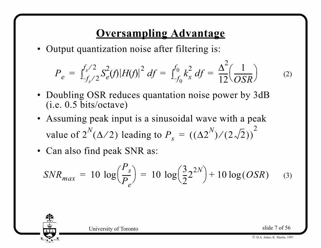
Oversampling Advantage • Output quantization noise after filtering is:
(2)
• Doubling OSR reduces quantation noise power by 3dB (i.e. 0.5 bits/octave)
• Assuming peak input is a sinusoidal wave with a peak
value of leading to
• Can also find peak SNR as:
(3)
Pe Se2 f( ) H f( ) 2 dffs 2⁄–
fs 2⁄∫ kx
2 dff0–f0∫
∆2
12------ 1OSR----------- = = =
2N ∆ 2⁄( ) Ps ∆2N( ) 2 2( )⁄( )2
=
SNRmax 10 PsPe----- log 10 3
2---22N log 10 OSR( )log+= =
slide 8 of 56University of Toronto© D.A. Johns, K. Martin, 1997
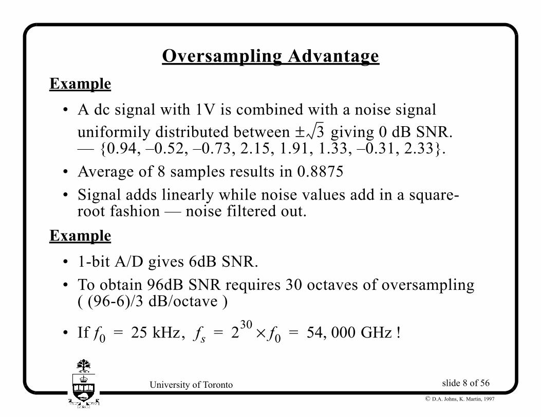
Oversampling AdvantageExample
• A dc signal with 1V is combined with a noise signal uniformily distributed between giving 0 dB SNR.— {0.94, –0.52, –0.73, 2.15, 1.91, 1.33, –0.31, 2.33}.
• Average of 8 samples results in 0.8875 • Signal adds linearly while noise values add in a square-
root fashion — noise filtered out.Example
• 1-bit A/D gives 6dB SNR. • To obtain 96dB SNR requires 30 octaves of oversampling
( (96-6)/3 dB/octave )
• If ,
3±
f0 25 kHz= fs 230 f0× 54 000 GHz !,= =
slide 9 of 56University of Toronto© D.A. Johns, K. Martin, 1997
Advantage of 1-bit D/A Converters • Oversampling improves SNR but not linearity • To acheive 16-bit linear converter using a 12-bit converter,
12-bit converter must be linear to 16 bits— i.e. integral nonlinearity better than LSB
• A 1-bit D/A is inherently linear— 1-bit D/A has only 2 output points— 2 points always lie on a straight line
• Can acheive better than 20 bits linearity without trimming (will likely have gain and offset error)
• Second-order effects (such as D/A memory or signal-dependent reference voltages) will limit linearity.
1 24⁄
slide 10 of 56University of Toronto© D.A. Johns, K. Martin, 1997
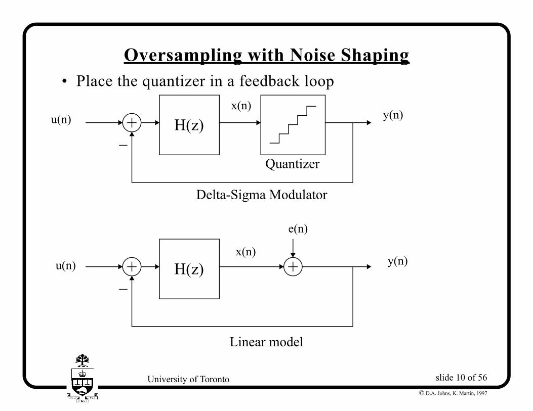
Oversampling with Noise Shaping • Place the quantizer in a feedback loop
H z( )–
x n( )u n( ) y n( )
H z( )–
x n( )u n( ) y n( )
e n( )
Quantizer
Delta-Sigma Modulator
Linear model
slide 11 of 56University of Toronto© D.A. Johns, K. Martin, 1997
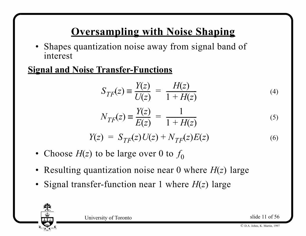
Oversampling with Noise Shaping • Shapes quantization noise away from signal band of
interestSignal and Noise Transfer-Functions
(4)
(5)
(6)
• Choose to be large over 0 to
• Resulting quantization noise near 0 where large • Signal transfer-function near 1 where large
STF z( ) Y z( )U z( )----------≡ H z( )
1 H z( )+--------------------=
NTF z( ) Y z( )E z( )----------≡ 1
1 H z( )+--------------------=
Y z( ) STF z( )U z( ) NTF z( )E z( )+=
H z( ) f0H z( )
H z( )
slide 12 of 56University of Toronto© D.A. Johns, K. Martin, 1997
Oversampling with Noise Shaping • Input signal is limited to range of quantizer output when
large • For 1-bit quantizers, input often limited to 1/4 quantizer
outputs • Out-of-band signals can be larger when small • Stability of modulator can be an issue (particularily for
higher-orders of • Stability defined as when input to quantizer becomes so
large that quantization error greater than — said to “overload the quantizer”
H z( )
H z( )
H z( )
∆ 2⁄±
slide 13 of 56University of Toronto© D.A. Johns, K. Martin, 1997
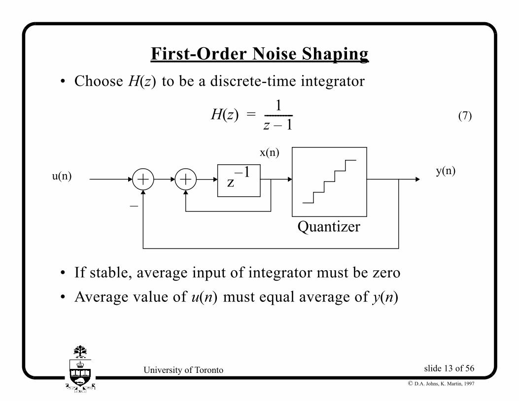
First-Order Noise Shaping • Choose to be a discrete-time integrator
(7)
• If stable, average input of integrator must be zero • Average value of must equal average of
H z( )
H z( ) 1z 1–-----------=
–
x n( )
u n( ) y n( )
Quantizer
z 1–
u n( ) y n( )
slide 14 of 56University of Toronto© D.A. Johns, K. Martin, 1997
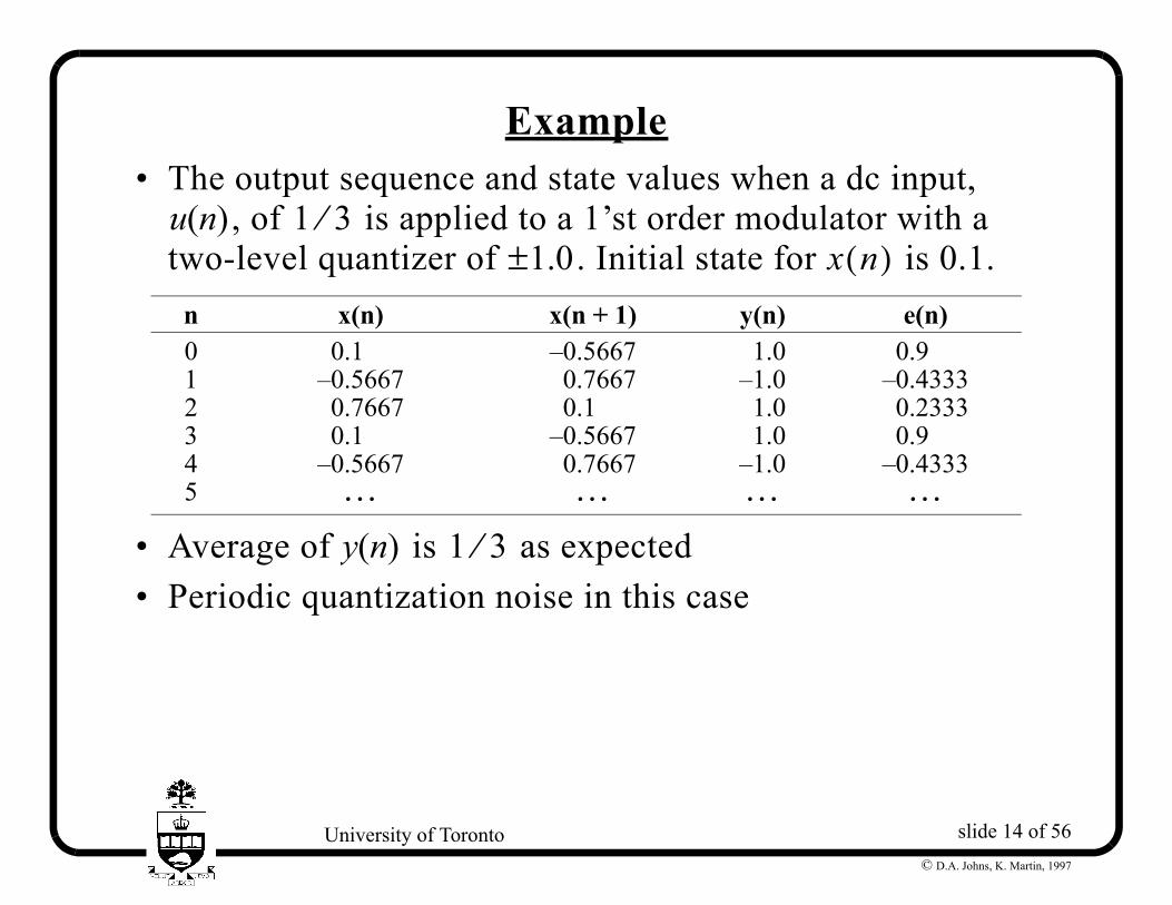
Example • The output sequence and state values when a dc input,
, of is applied to a 1’st order modulator with a two-level quantizer of . Initial state for is 0.1.
• Average of is as expected • Periodic quantization noise in this case
n x(n) x(n + 1) y(n) e(n)0 –0.1000 –0.5667 –1.0 –0.90001 –0.5667 –0.7667 –1.0 –0.43332 –0.7667 –0.1000 –1.0 –0.23333 –0.1000 –0.5667 –1.0 –0.90004 –0.5667 –0.7667 –1.0 –0.43335
u n( ) 1 3⁄1.0± x n( )
… … … …y n( ) 1 3⁄
slide 15 of 56University of Toronto© D.A. Johns, K. Martin, 1997
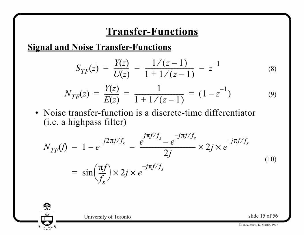
Transfer-FunctionsSignal and Noise Transfer-Functions
(8)
(9)
• Noise transfer-function is a discrete-time differentiator (i.e. a highpass filter)
(10)
STF z( ) Y z( )U z( )---------- 1 z 1–( )⁄
1 1 z 1–( )⁄+-------------------------------- z 1–= = =
NTF z( ) Y z( )E z( )---------- 1
1 1 z 1–( )⁄+-------------------------------- 1 z 1––( )= = =
NTF f( ) 1 ej– 2πf fs⁄
– ejπf fs⁄
ejπf– fs⁄
–2j------------------------------------ 2j e
jπf– fs⁄××= =
πffs----- sin 2j e
jπf– fs⁄××=
slide 16 of 56University of Toronto© D.A. Johns, K. Martin, 1997
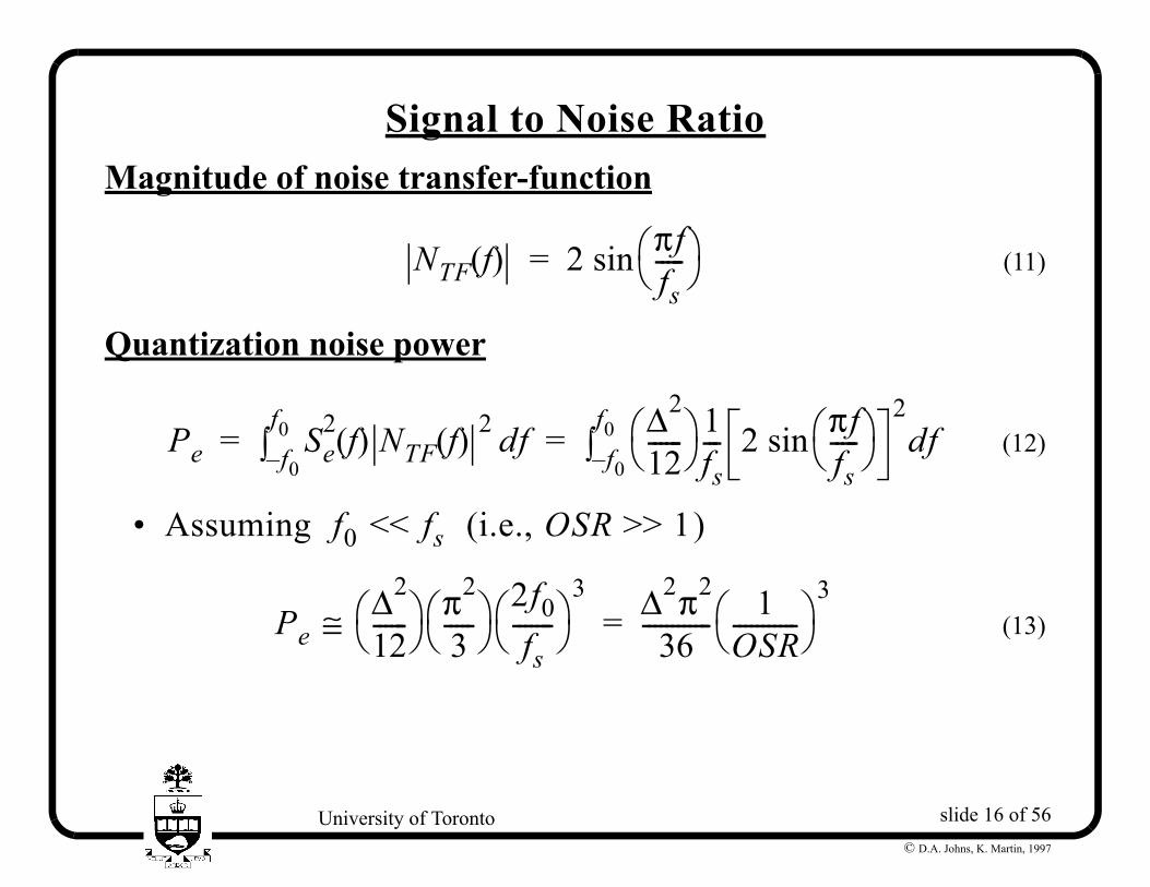
Signal to Noise RatioMagnitude of noise transfer-function
(11)
Quantization noise power
(12)
• Assuming (i.e., )
(13)
NTF f( ) 2 πffs----- sin=
Pe Se2 f( ) NTF f( ) 2 dff0–
f0∫
∆2
12------ 1
fs--- 2 πf
fs----- sin
2dff0–
f0∫= =
f0 << fs OSR >> 1
Pe∆2
12------ π2
3----- 2f0
fs-------
3≅ ∆2π2
36------------ 1OSR-----------
3=
slide 17 of 56University of Toronto© D.A. Johns, K. Martin, 1997
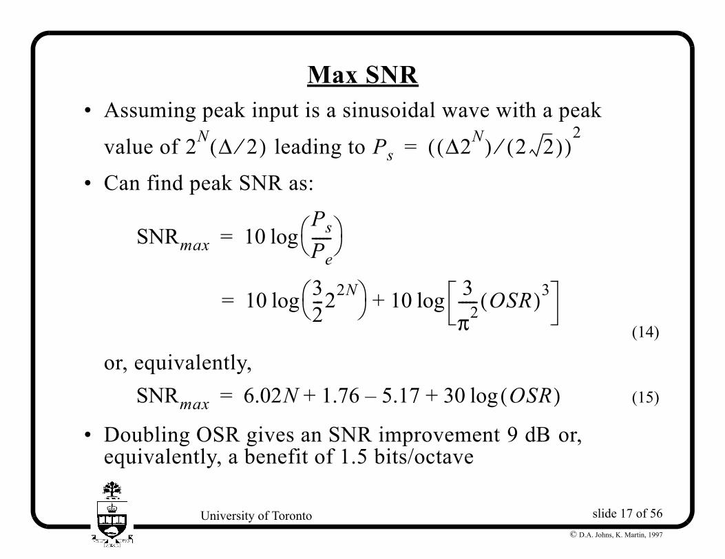
Max SNR • Assuming peak input is a sinusoidal wave with a peak
value of leading to
• Can find peak SNR as:
(14)
or, equivalently,(15)
• Doubling OSR gives an SNR improvement or, equivalently, a benefit of 1.5 bits/octave
2N ∆ 2⁄( ) Ps ∆2N( ) 2 2( )⁄( )2
=
SNRmax 10PsPe----- log=
10 32---22N log 10 3
π2----- OSR( )3log+=
SNRmax 6.02N 1.76 5.17– 30 OSR( )log+ +=
9 dB
slide 18 of 56University of Toronto© D.A. Johns, K. Martin, 1997
SC Implementation
1-bit D/A
–u n( ) y n( )
Quantizer
z 1–
Analog Digital
H z( )
Vref 2⁄
VinVout
C
C
φ2
φ2
φ1
φ1
φ2 φ1( ),
φ1 φ2( ),
Latch on φ2 falling
φ1 φ2, Vout high↔φ1( ) φ2( ), Vout low↔
ComparatorC
slide 19 of 56University of Toronto© D.A. Johns, K. Martin, 1997
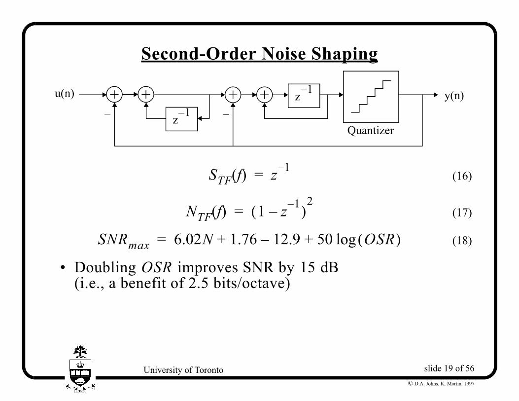
Second-Order Noise Shaping
(16)
(17)
(18)
• Doubling improves SNR by (i.e., a benefit of 2.5 bits/octave)
–
u n( ) y n( )
Quantizer
z 1–
– z 1–
STF f( ) z 1–=
NTF f( ) 1 z 1––( )2
=
SNRmax 6.02N 1.76 12.9– 50 OSR( )log+ +=
OSR 15 dB
slide 20 of 56University of Toronto© D.A. Johns, K. Martin, 1997
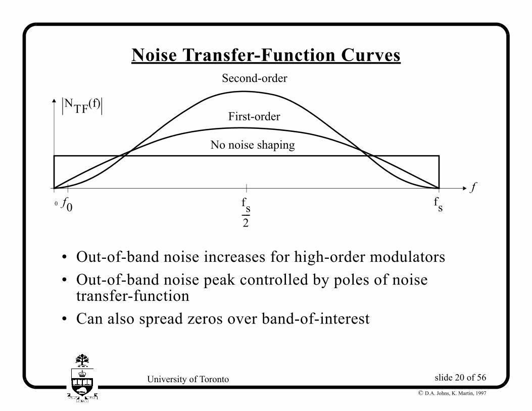
Noise Transfer-Function Curves
• Out-of-band noise increases for high-order modulators • Out-of-band noise peak controlled by poles of noise
transfer-function • Can also spread zeros over band-of-interest
0 f0 fsfs2----
NTF f( )First-order
Second-order
No noise shaping
f
slide 21 of 56University of Toronto© D.A. Johns, K. Martin, 1997
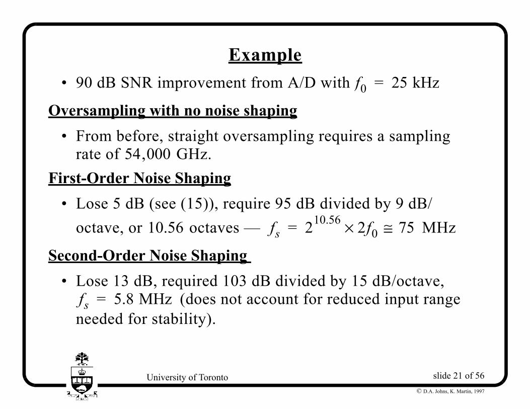
Example • 90 dB SNR improvement from A/D with
Oversampling with no noise shaping • From before, straight oversampling requires a sampling
rate of GHz.First-Order Noise Shaping
• Lose 5 dB (see (15)), require 95 dB divided by 9 dB/octave, or octaves — MHz
Second-Order Noise Shaping • Lose 13 dB, required 103 dB divided by 15 dB/octave,
(does not account for reduced input range needed for stability).
f0 25 kHz=
54,000
10.56 fs 210.56 2f0× 75≅=
fs 5.8 MHz=
slide 22 of 56University of Toronto© D.A. Johns, K. Martin, 1997
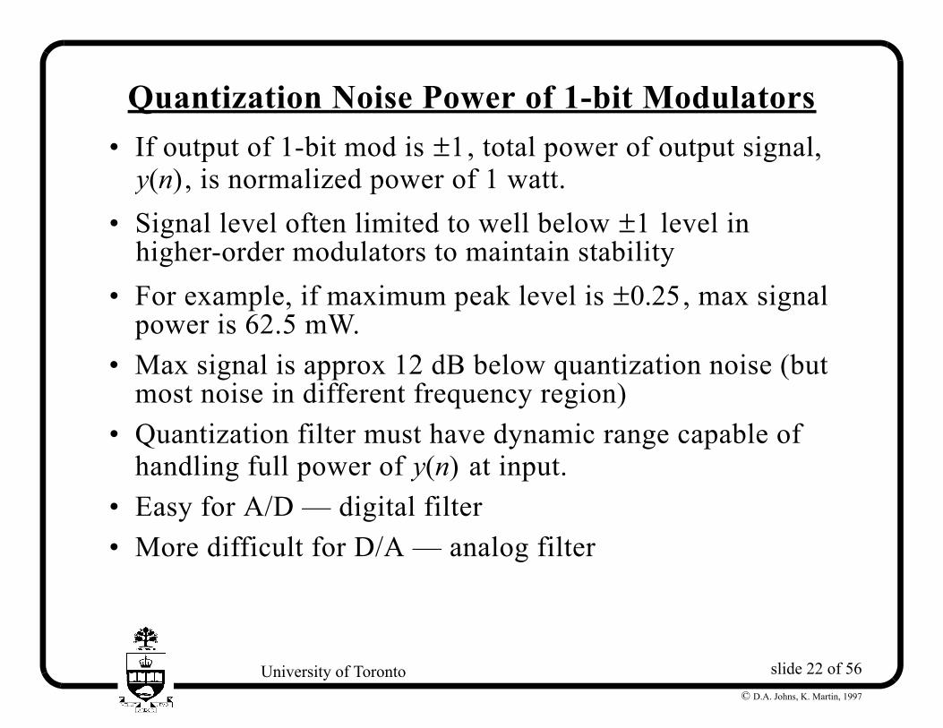
Quantization Noise Power of 1-bit Modulators • If output of 1-bit mod is , total power of output signal,
, is normalized power of 1 watt. • Signal level often limited to well below level in
higher-order modulators to maintain stability • For example, if maximum peak level is , max signal
power is 62.5 mW. • Max signal is approx 12 dB below quantization noise (but
most noise in different frequency region) • Quantization filter must have dynamic range capable of
handling full power of at input. • Easy for A/D — digital filter • More difficult for D/A — analog filter
1±y n( )
1±
0.25±
y n( )
slide 23 of 56University of Toronto© D.A. Johns, K. Martin, 1997
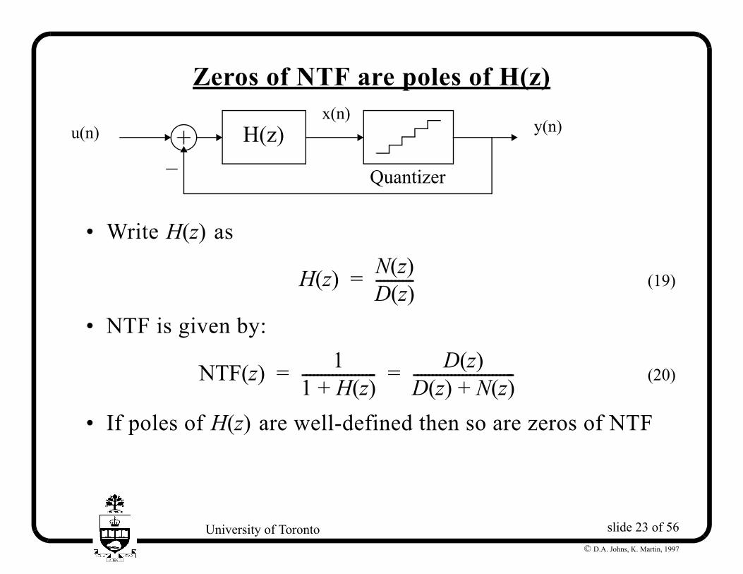
Zeros of NTF are poles of H(z)
• Write as
(19)
• NTF is given by:
(20)
• If poles of are well-defined then so are zeros of NTF
H z( )–
x n( )u n( ) y n( )
Quantizer
H z( )
H z( ) N z( )D z( )----------=
NTF z( ) 11 H z( )+-------------------- D z( )
D z( ) N z( )+---------------------------= =
H z( )
slide 24 of 56University of Toronto© D.A. Johns, K. Martin, 1997
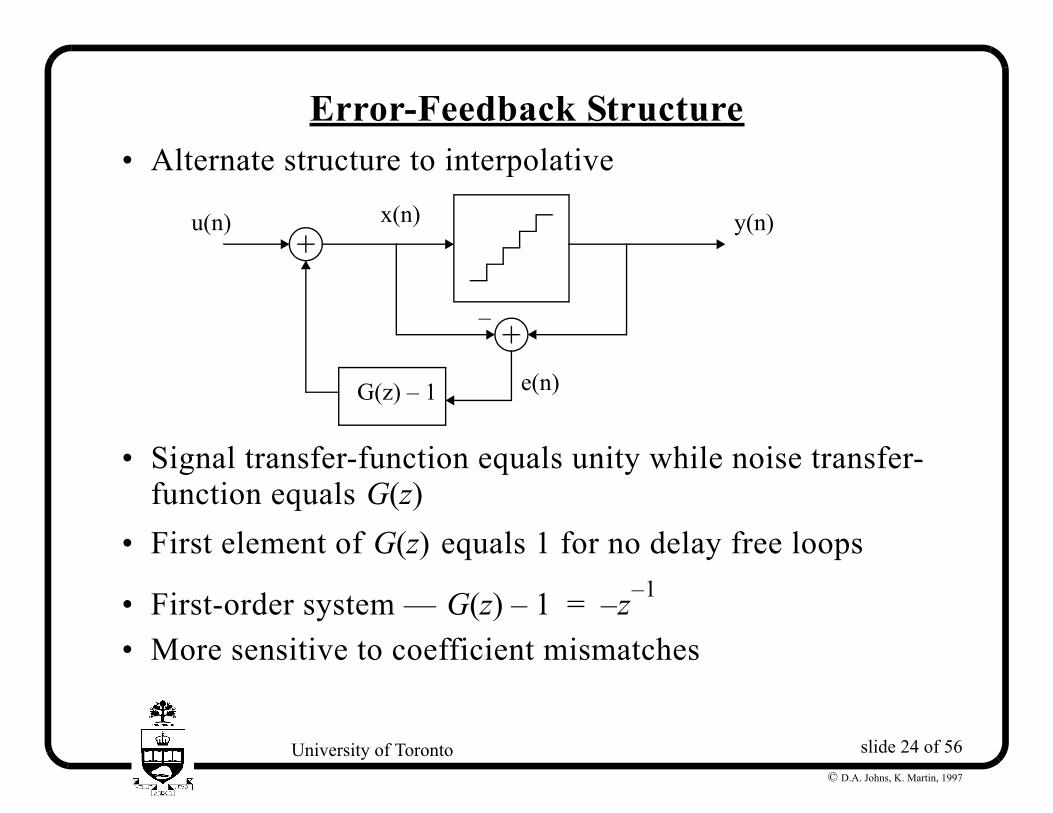
Error-Feedback Structure • Alternate structure to interpolative
• Signal transfer-function equals unity while noise transfer-function equals
• First element of equals 1 for no delay free loops
• First-order system — • More sensitive to coefficient mismatches
G z( ) 1–
y n( )
e n( )
x n( )u n( )
–
G z( )G z( )
G z( ) 1– z– 1–=
slide 25 of 56University of Toronto© D.A. Johns, K. Martin, 1997
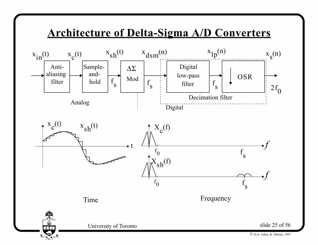
Architecture of Delta-Sigma A/D Converters
Sample-and-
Digital
filterholdlow-passMod
∆Σ
xsh t( ) xlp n( ) xs n( )xc t( )
fs fs fs 2f0
xdsm n( )
OSRAnti-
aliasingfilter
xin t( )
AnalogDigital
Decimation filter
xc t( )
t f
Xc f( )xsh t( )
fXsh f( )
fsf0
fsf0
Time Frequency
slide 26 of 56University of Toronto© D.A. Johns, K. Martin, 1997
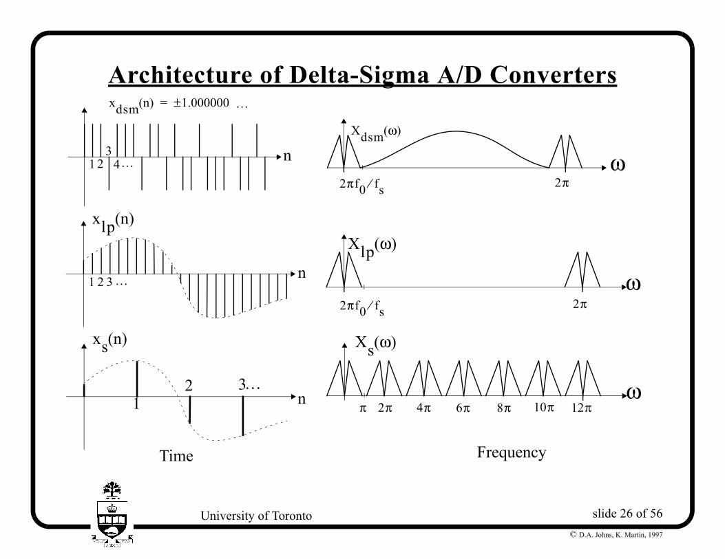
Architecture of Delta-Sigma A/D Converters
Time Frequency
xlp n( )
n ω
Xlp ω( )
xs n( )
n ω
Xs ω( )
2π2πf0 fs⁄
2ππ 4π 6π 8π 10π 12π12 3
1 2 3 …
…
n
xdsm n( ) 1.000000±=
1 23
4 …
…
ωXdsm ω( )
2π2πf0 fs⁄
slide 27 of 56University of Toronto© D.A. Johns, K. Martin, 1997
Architecture of Delta-Sigma A/D Converters • Relaxes analog anti-aliasing filter • Strict anti-aliasing done in digital domain • Must also remove quantization noise before
downsampling (or aliasing occurs) • Commonly done with a multi-stage system • Linearity of D/A in modulator important — results in
overall nonlinearity • Linearity of A/D in modulator unimportant (effects
reduced by high gain in feedback of modulator)
slide 28 of 56University of Toronto© D.A. Johns, K. Martin, 1997
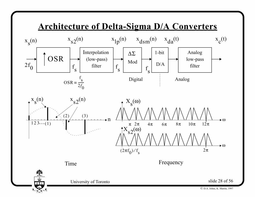
Architecture of Delta-Sigma D/A Converters
Interpolation
filter(low-pass) Mod
∆Σ 1-bit
D/A
Analog
filterlow-pass
AnalogDigital
xs n( ) xs2 n( ) xlp n( ) xdsm n( ) xda t( ) xc t( )
2f0 fs fs fs
OSRfs
2f0--------≡
OSR
n
ω
ω
Xs ω( )
Xs2 ω( )
xs n( ) xs2 n( )
2ππ 4π 6π 8π 10π 12π
2π2πf0( ) fs⁄
1 2 3 1( )
2( ) 3( )…
Time Frequency
slide 29 of 56University of Toronto© D.A. Johns, K. Martin, 1997
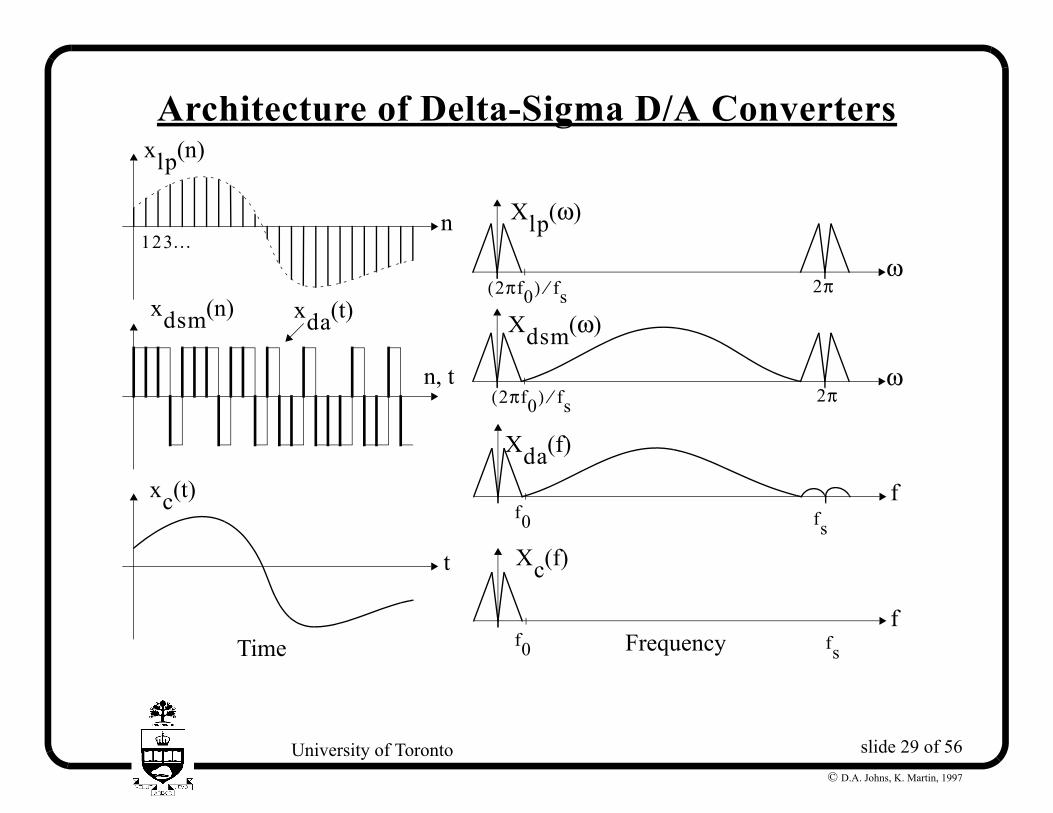
Architecture of Delta-Sigma D/A Convertersxlp n( )
xdsm n( ) xda t( )
xc t( )
n
n t,
t
f
f
ω
ω
Xlp ω( )
Xdsm ω( )
Xda f( )
Xc f( )
Time Frequency
fs
fsf0
f0
2π2πf0( ) fs⁄
2π2πf0( ) fs⁄
123…
slide 30 of 56University of Toronto© D.A. Johns, K. Martin, 1997
Architecture of Delta-Sigma D/A Converters • Relaxes analog smoothing filter (many multibit D/A
converters are oversampled without noise shaping) • Smoothing filter of first few images done in digital (then
often below quantization noise) • Order of lowpass filter should be at least one order higher
than that of modulator • Results in noise dropping off (rather than flat) • Analog filter must attenuate quantization noise and should
not modulate noise back to low freq — strong motivation to use multibit quantizers
slide 31 of 56University of Toronto© D.A. Johns, K. Martin, 1997
Multi-Stage Digital Decimation
• Sinc filter removes much of quantization noise • Following filter(s) — anti-aliasing filter and noise
FIR filterSincL 1+ IIR filter
Rate fs= Rate 8f0= Rate 2f0=
∆Σmodulator
Lth-orderTsinc z( ) TIIR z( )
FIR filterSincL 1+ Halfband FIR filters
Rate fs= Rate 8f0= Rate 2f0=
∆Σmodulator
Lth-orderTsinc z( )
Rate 4f0=
H1 z( ) H2 z( ) H3 z( )
Sinc compensationFIR filter
Rate 2f0=
slide 32 of 56University of Toronto© D.A. Johns, K. Martin, 1997
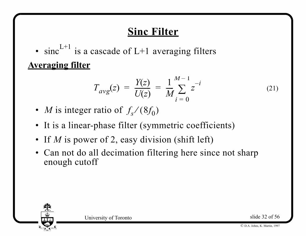
Sinc Filter
• is a cascade of averaging filtersAveraging filter
(21)
• is integer ratio of
• It is a linear-phase filter (symmetric coefficients) • If is power of 2, easy division (shift left) • Can not do all decimation filtering here since not sharp
enough cutoff
sincL+1 L+1
Tavg z( ) Y z( )U z( )---------- 1
M----- z i–
i 0=
M 1–
∑= =
M fs 8f0( )⁄
M
slide 33 of 56University of Toronto© D.A. Johns, K. Martin, 1997
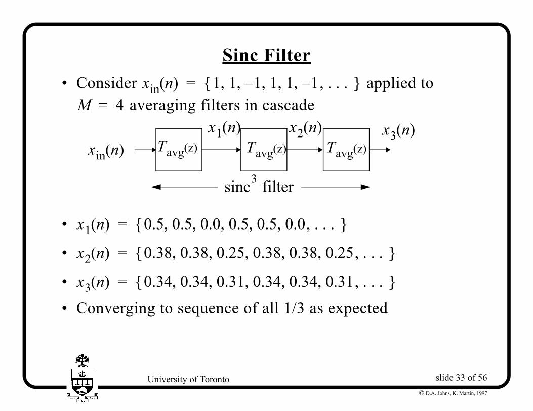
Sinc Filter • Consider applied to
averaging filters in cascade
•
•
•
• Converging to sequence of all 1/3 as expected
xin n( ) 1 1 1– 1 1 1– , . . ., , , , ,{ }=M 4=
Tavg z( ) Tavg z( ) Tavg z( )xin n( )x1 n( ) x2 n( ) x3 n( )
sinc3 filter
x1 n( ) 0.5 0.5 0.0 0.5 0.5 0.0, . . ., , , , ,{ }=
x2 n( ) 0.38 0.38 0.25 0.38 0.38 0.25, . . ., , , , ,{ }=
x3 n( ) 0.34 0.34 0.31 0.34 0.34 0.31, . . ., , , , ,{ }=
slide 34 of 56University of Toronto© D.A. Johns, K. Martin, 1997
Sinc Filter Response • Can rewrite averaging filter in recursive form as
(22)
and a cascade of averaging filters results in
(23)
• Use cascade to roll off quantization noise faster than it rises in ‘th order modulator
Tavg z( ) Y z( )U z( )---------- 1
M-----1 z M––1 z 1––-----------------
= =
L 1+
Tsinc z( ) 1ML 1+-------------- 1 z M––
1 z 1––----------------- L 1+
=
L 1+L
slide 35 of 56University of Toronto© D.A. Johns, K. Martin, 1997
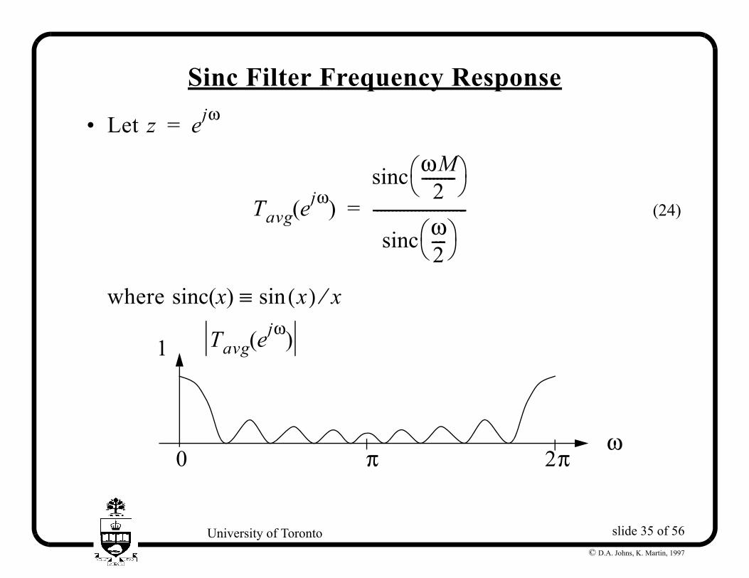
Sinc Filter Frequency Response
• Let
(24)
where
z ejω=
Tavg ejω( )
sinc ωM2---------
sinc ω2----
-------------------------=
sinc x( ) x( )sin x⁄≡
2ππ0ω
Tavg ejω( )1
slide 36 of 56University of Toronto© D.A. Johns, K. Martin, 1997
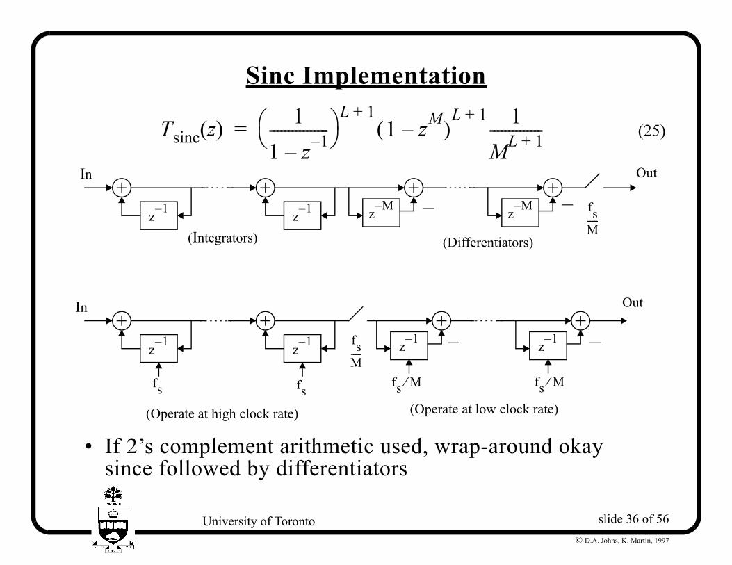
Sinc Implementation
(25)
• If 2’s complement arithmetic used, wrap-around okay since followed by differentiators
Tsinc z( ) 11 z 1––---------------- L 1+
1 zM–( )L 1+ 1
ML 1+--------------=
z 1– z 1– z M– z M– fsM-----
OutIn
z 1– z 1– fsM----- z 1– z 1–
(Operate at low clock rate)
OutIn
(Operate at high clock rate)
(Integrators) (Differentiators)
––
– –
fs M⁄ fs M⁄fsfs
slide 37 of 56University of Toronto© D.A. Johns, K. Martin, 1997
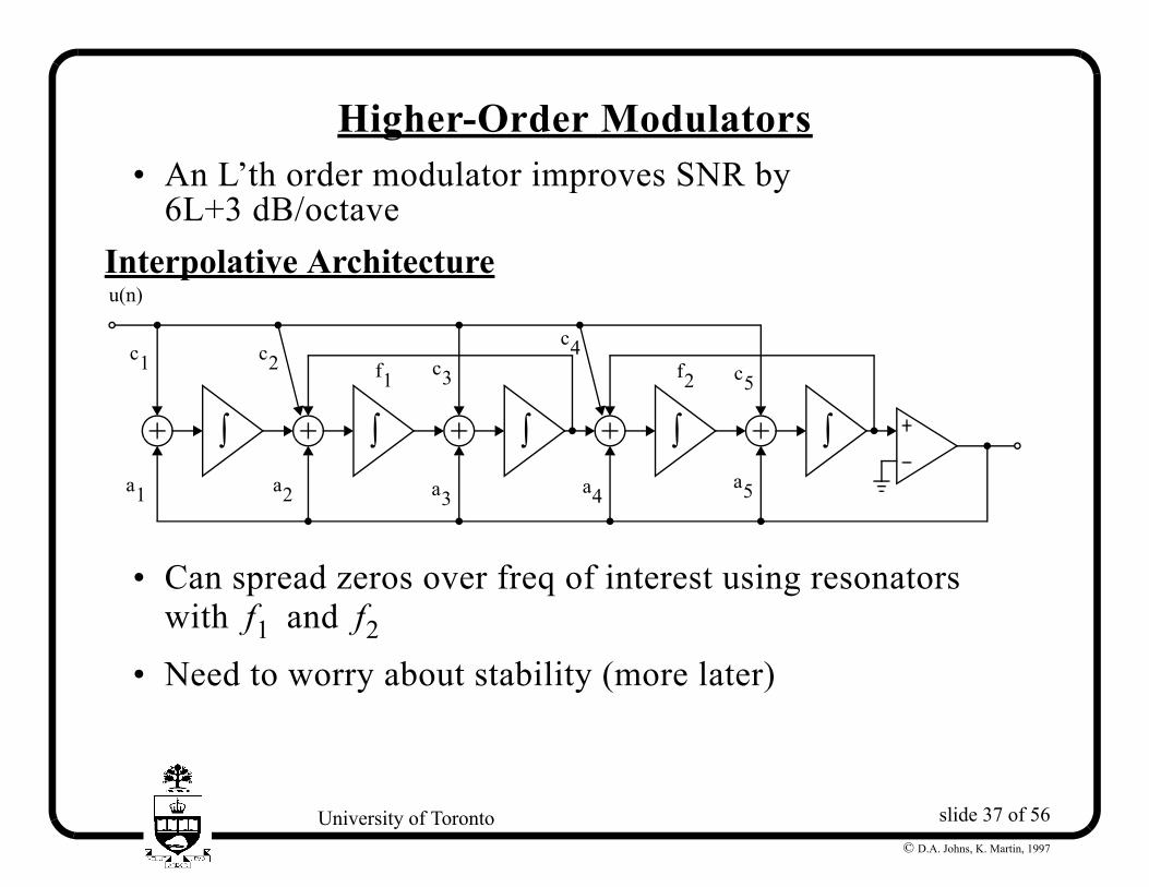
Higher-Order Modulators • An L’th order modulator improves SNR by
6L+3 dB/octaveInterpolative Architecture
• Can spread zeros over freq of interest using resonators with and
• Need to worry about stability (more later)
∫ ∫ ∫ ∫ ∫
u n( )
a1 a2 a3 a4
c1 c2 c3f1 f2
c4c5
a5
f1 f2
slide 38 of 56University of Toronto© D.A. Johns, K. Martin, 1997
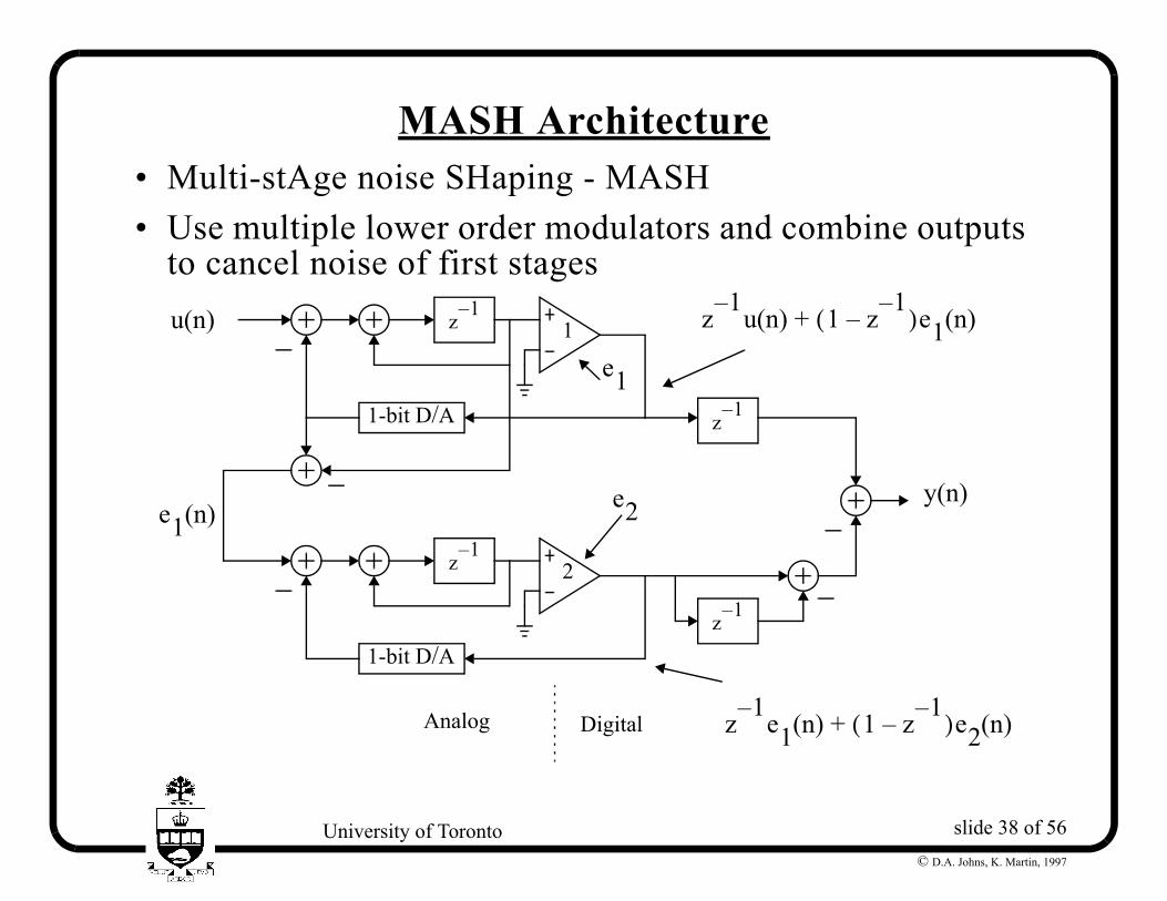
MASH Architecture • Multi-stAge noise SHaping - MASH • Use multiple lower order modulators and combine outputs
to cancel noise of first stagesz 1–
1-bit D/A
z 1–
1-bit D/A
z 1–
z 1–
1
2
e1
e2y n( )
u n( )
e1 n( )
z 1– u n( ) 1 z 1––( )e1 n( )+
z 1– e1 n( ) 1 z 1––( )e2 n( )+Analog Digital
slide 39 of 56University of Toronto© D.A. Johns, K. Martin, 1997
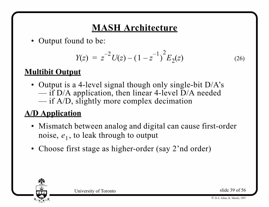
MASH Architecture • Output found to be:
(26)
Multibit Output • Output is a 4-level signal though only single-bit D/A’s
— if D/A application, then linear 4-level D/A needed— if A/D, slightly more complex decimation
A/D Application • Mismatch between analog and digital can cause first-order
noise, , to leak through to output
• Choose first stage as higher-order (say 2’nd order)
Y z( ) z 2– U z( ) 1 z 1––( )2E2 z( )–=
e1
slide 40 of 56University of Toronto© D.A. Johns, K. Martin, 1997
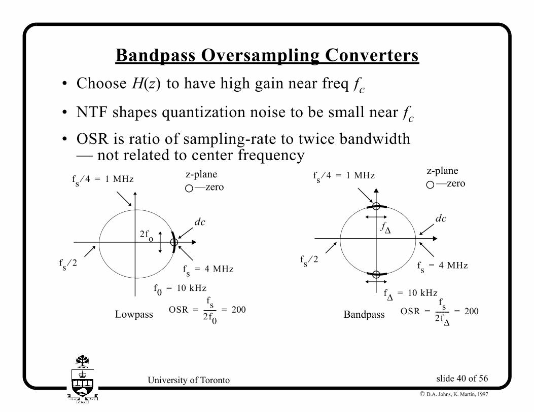
Bandpass Oversampling Converters • Choose to have high gain near freq
• NTF shapes quantization noise to be small near
• OSR is ratio of sampling-rate to twice bandwidth — not related to center frequency
H z( ) fcfc
z-plane
Bandpass
fs 2⁄ fs 4 MHz=
dc
fs 4⁄ 1 MHz=—zero
f∆ 10 kHz=
z-plane
fs 4 MHz=
dc
fs 4⁄ 1 MHz=—zero
f0 10 kHz=
fs 2⁄
Lowpass
f∆2fo
OSRfs
2f0-------- 200= = OSR
fs2f∆--------- 200= =
slide 41 of 56University of Toronto© D.A. Johns, K. Martin, 1997
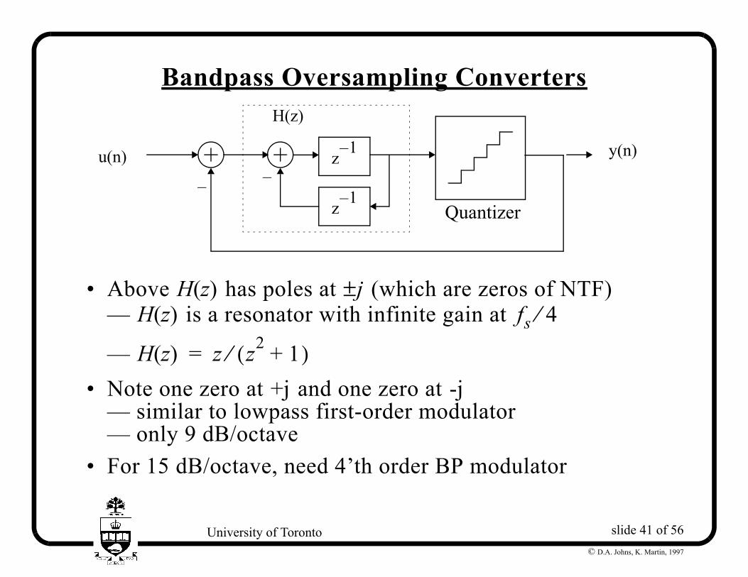
Bandpass Oversampling Converters
• Above has poles at (which are zeros of NTF)— is a resonator with infinite gain at
— • Note one zero at and one zero at
— similar to lowpass first-order modulator— only 9 dB/octave
• For 15 dB/octave, need 4’th order BP modulator
–
u n( ) y n( )
Quantizer
z 1–
z 1–
H z( )
–
H z( ) j±H z( ) fs 4⁄
H z( ) z z2 1+( )⁄=+j -j
slide 42 of 56University of Toronto© D.A. Johns, K. Martin, 1997
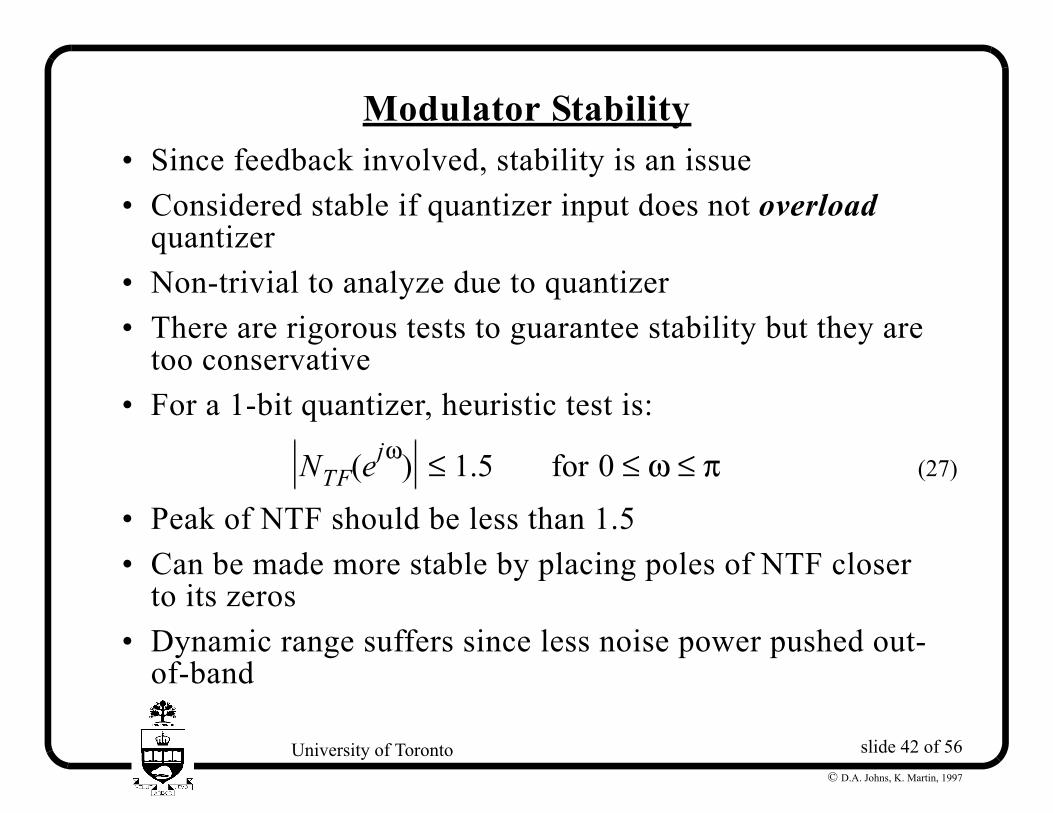
Modulator Stability • Since feedback involved, stability is an issue • Considered stable if quantizer input does not overload
quantizer • Non-trivial to analyze due to quantizer • There are rigorous tests to guarantee stability but they are
too conservative • For a 1-bit quantizer, heuristic test is:
(27)
• Peak of NTF should be less than 1.5 • Can be made more stable by placing poles of NTF closer
to its zeros • Dynamic range suffers since less noise power pushed out-
of-band
NTF ejω( ) 1.5 for 0 ω π≤ ≤≤
slide 43 of 56University of Toronto© D.A. Johns, K. Martin, 1997
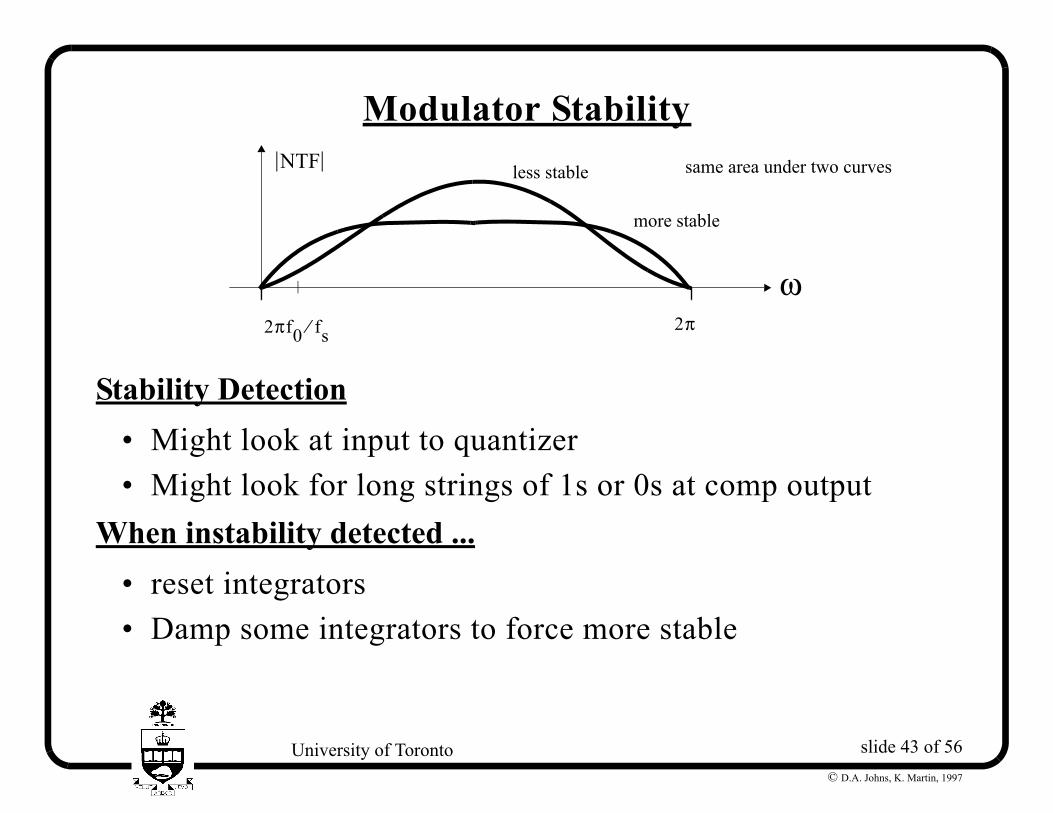
Modulator Stability
Stability Detection • Might look at input to quantizer • Might look for long strings of 1s or 0s at comp output
When instability detected ... • reset integrators • Damp some integrators to force more stable
ω2π2πf0 fs⁄
NTF less stable
more stable
same area under two curves
slide 44 of 56University of Toronto© D.A. Johns, K. Martin, 1997
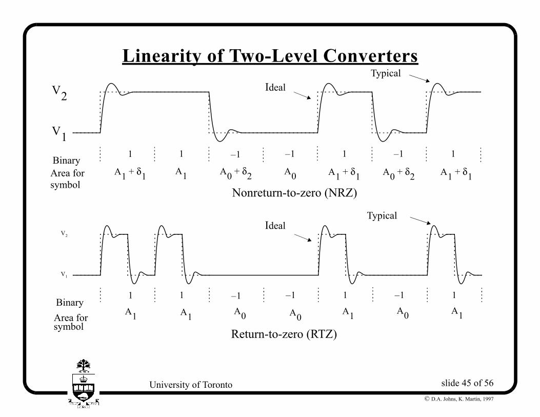
Linearity of Two-Level Converters • For high-linearity, levels should NOT be a function of
input signal — power supply variation might cause symptom
• Also need to be memoryless — switched-capacitor circuits are inherently memoryless if enough settling-time allowed
• Above linearity issues also applicable to multi-level • A nonreturn-to-zero is NOT memoryless • Return-to-zero is memoryless if enough settling time • Important for continuous-time D/A
slide 45 of 56University of Toronto© D.A. Johns, K. Martin, 1997
Linearity of Two-Level Converters
A1 δ1+ A1
1 1– 1– 1–1 1 1
A0 δ2+ A0
V2
V1
BinaryArea forsymbol
A1 δ1+ A1 δ1+A0 δ2+
IdealTypical
IdealTypical
A1 A1
1 1– 1– 1–1 1 1
A0
V2
V1
BinaryArea forsymbol
A0 A1 A1A0
Nonreturn-to-zero (NRZ)
Return-to-zero (RTZ)
slide 46 of 56University of Toronto© D.A. Johns, K. Martin, 1997
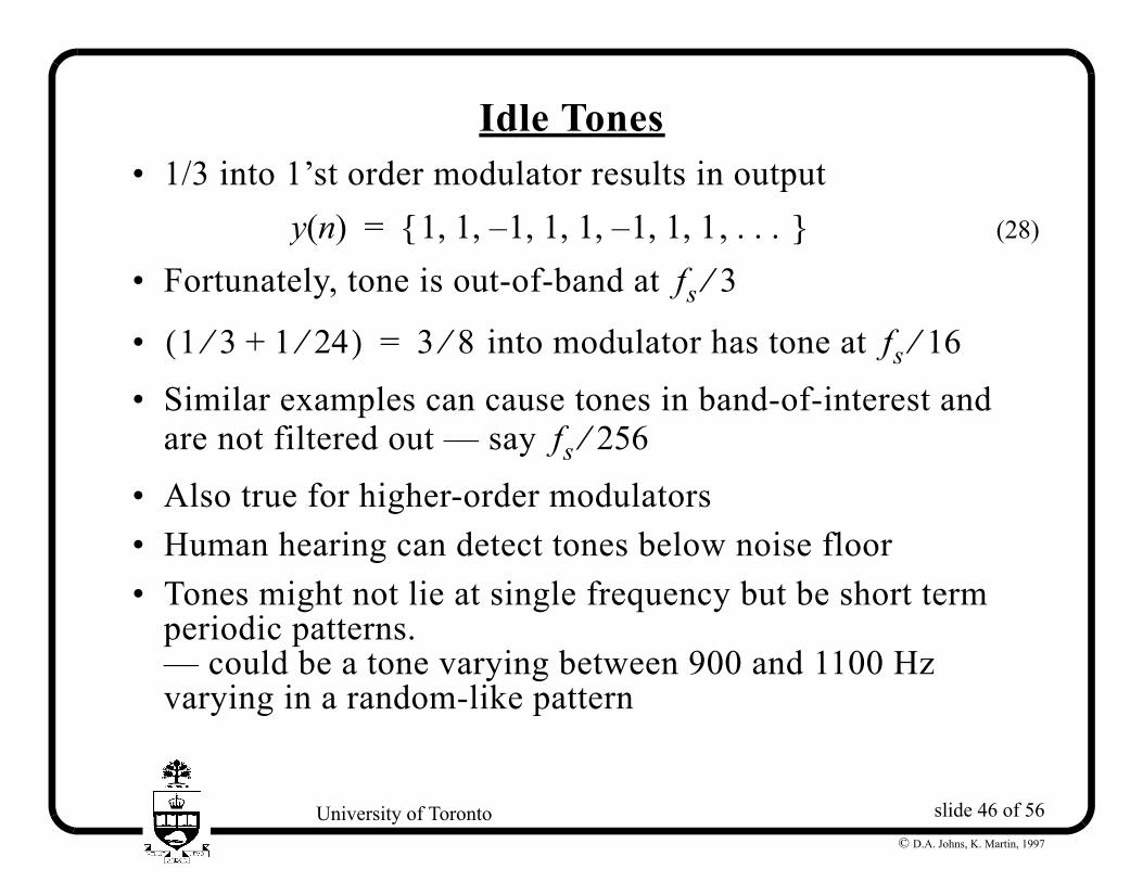
Idle Tones • 1/3 into 1’st order modulator results in output
(28)
• Fortunately, tone is out-of-band at
• into modulator has tone at
• Similar examples can cause tones in band-of-interest and are not filtered out — say
• Also true for higher-order modulators • Human hearing can detect tones below noise floor • Tones might not lie at single frequency but be short term
periodic patterns.— could be a tone varying between 900 and 1100 Hz varying in a random-like pattern
y n( ) 1 1 1– 1 1 1– 1 1, . . ., , , , , , ,{ }=fs 3⁄
1 3⁄ 1 24⁄+( ) 3 8⁄= fs 16⁄
fs 256⁄
slide 47 of 56University of Toronto© D.A. Johns, K. Martin, 1997
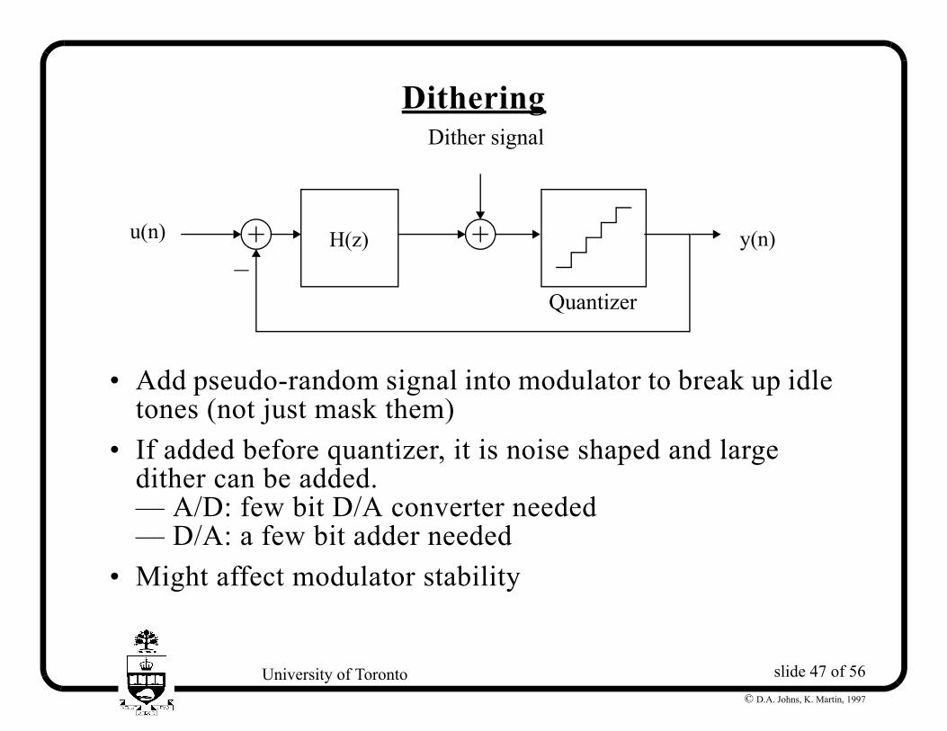
Dithering
• Add pseudo-random signal into modulator to break up idle tones (not just mask them)
• If added before quantizer, it is noise shaped and large dither can be added.— A/D: few bit D/A converter needed— D/A: a few bit adder needed
• Might affect modulator stability
H z( )–
u n( ) y n( )
Quantizer
Dither signal
slide 48 of 56University of Toronto© D.A. Johns, K. Martin, 1997
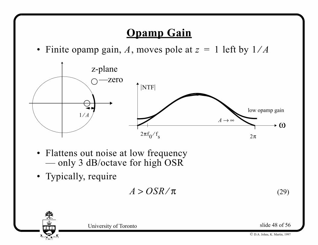
Opamp Gain • Finite opamp gain, , moves pole at left by
• Flattens out noise at low frequency— only 3 dB/octave for high OSR
• Typically, require (29)
A z 1= 1 A⁄
z-plane—zero
1 A⁄
ω2π
NTF
low opamp gain
A ∞→
2πf0 fs⁄
A OSR π⁄>
slide 49 of 56University of Toronto© D.A. Johns, K. Martin, 1997
Multi-bit Oversampled Converters • A multi-bit DAC has many advantages
— more stable - higher peak — higher input range— less quantization noise introduced— less idle tones (perhaps no dithering needed)
• Need highly linear multi-bit D/A convertersExample
• A 4-bit DAC has 18 dB less quantization noise, up to 12 dB higher input range — perhaps 30 dB improved SNR over 1-bit
Large Advantage in DAC Application • Less quantization noise — easier analog lowpass filter
NTF
slide 50 of 56University of Toronto© D.A. Johns, K. Martin, 1997
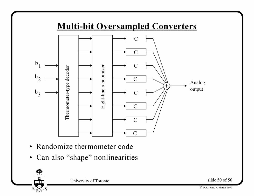
Multi-bit Oversampled Converters
• Randomize thermometer code • Can also “shape” nonlinearities
C
C
C
C
C
C
C
C
Eigh
t-lin
e ra
ndom
izer
Ther
mom
eter
-type
dec
oder
b1
b2
b3
Analogoutput
slide 51 of 56University of Toronto© D.A. Johns, K. Martin, 1997
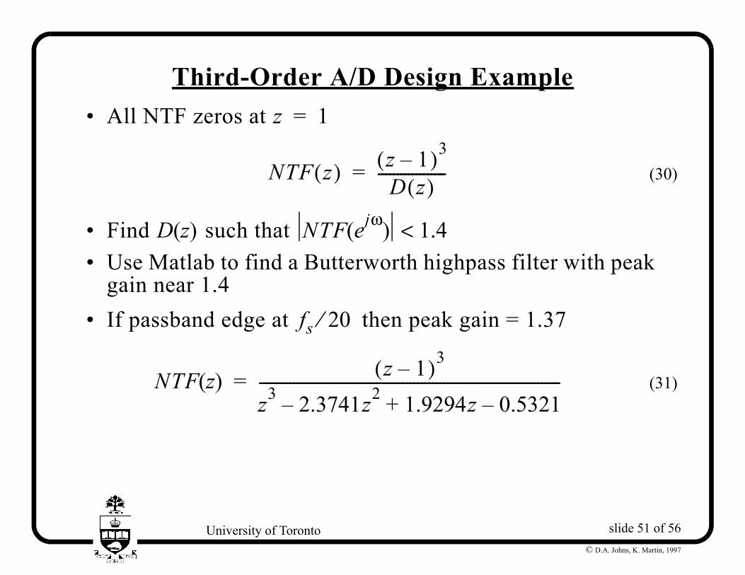
Third-Order A/D Design Example • All NTF zeros at
(30)
• Find such that • Use Matlab to find a Butterworth highpass filter with peak
gain near 1.4 • If passband edge at then peak gain = 1.37
(31)
z 1=
NTF z( ) z 1–( )3
D z( )------------------=
D z( ) NTF ejω( ) 1.4<
fs 20⁄
NTF z( ) z 1–( )3
z3 2.3741z2– 1.9294z 0.5321–+--------------------------------------------------------------------------------=
slide 52 of 56University of Toronto© D.A. Johns, K. Martin, 1997
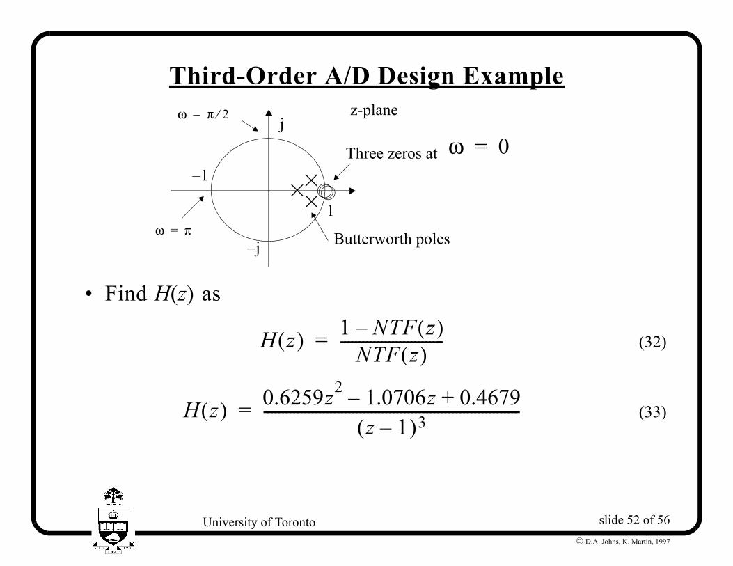
Third-Order A/D Design Example
• Find as
(32)
(33)
z-plane
–1
1
j
–j
ω 0=ω π 2⁄=
ω π=
Three zeros at
Butterworth poles
H z( )
H z( ) 1 NTF z( )–NTF z( )
----------------------------=
H z( ) 0.6259z2 1.0706z– 0.4679+z 1–( )3---------------------------------------------------------------------=
slide 53 of 56University of Toronto© D.A. Johns, K. Martin, 1997
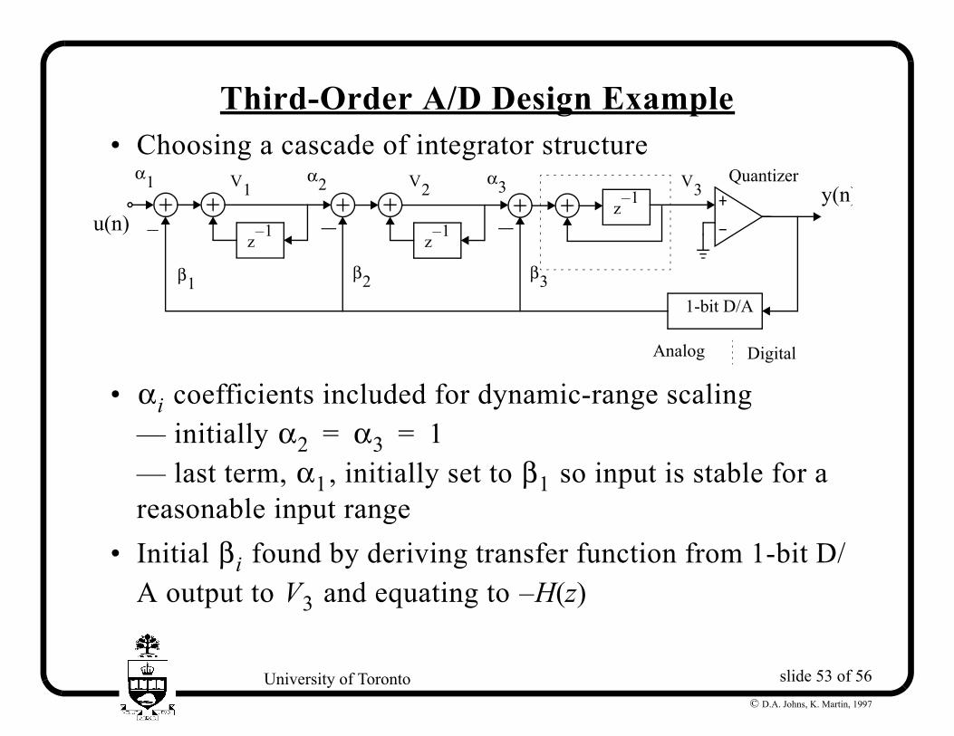
Third-Order A/D Design Example • Choosing a cascade of integrator structure
• coefficients included for dynamic-range scaling— initially — last term, , initially set to so input is stable for a reasonable input range
• Initial found by deriving transfer function from 1-bit D/A output to and equating to
1-bit D/A
–u n( )y n( )
Quantizer
z 1–
z 1–z 1– – –β1 β2 β3
α1 α2 α3 V3V2V1
Analog Digital
αiα2 α3 1= =
α1 β1
βiV3 H z( )–
slide 54 of 56University of Toronto© D.A. Johns, K. Martin, 1997
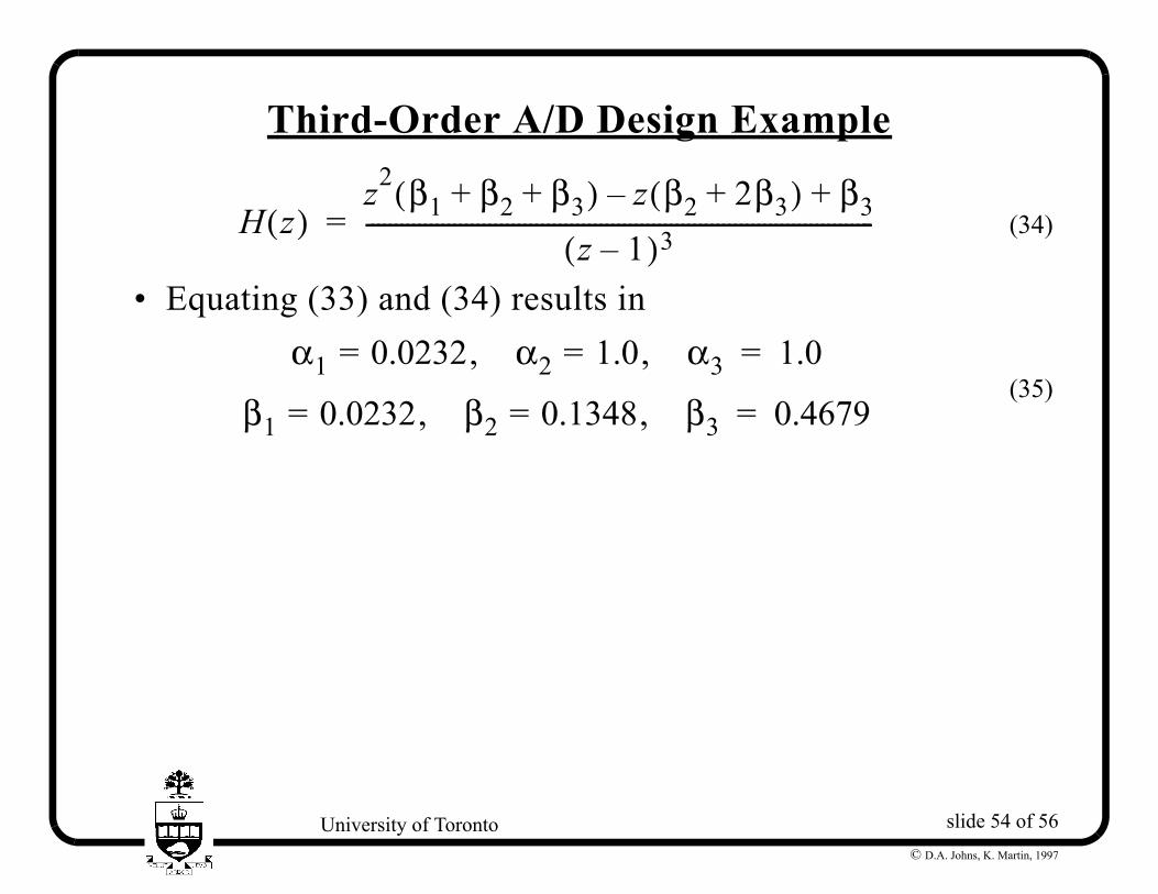
Third-Order A/D Design Example
(34)
• Equating (33) and (34) results in
(35)
H z( )z2 β1 β2 β3+ +( ) z β2 2β3+( )– β3+
z 1–( )3---------------------------------------------------------------------------------------=
α1 0.0232= , α2 1.0= , α3 1.0=
β1 0.0232= , β2 0.1348= , β3 0.4679=
slide 55 of 56University of Toronto© D.A. Johns, K. Martin, 1997
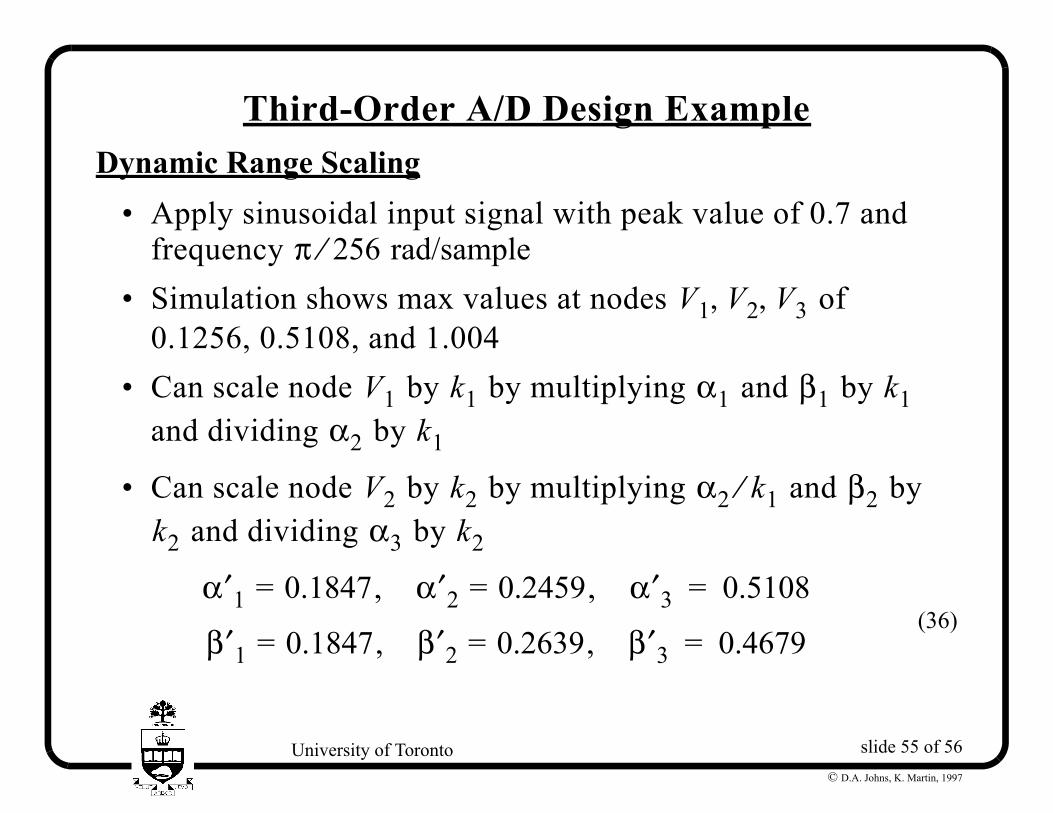
Third-Order A/D Design ExampleDynamic Range Scaling
• Apply sinusoidal input signal with peak value of 0.7 and frequency
• Simulation shows max values at nodes of 0.1256, 0.5108, and 1.004
• Can scale node by by multiplying and by and dividing by
• Can scale node by by multiplying and by and dividing by
(36)
π 256⁄ rad/sampleV1 V2 V3, ,
V1 k1 α1 β1 k1α2 k1
V2 k2 α2 k1⁄ β2k2 α3 k2
α′1 0.1847= , α′2 0.2459= , α′3 0.5108=
β′1 0.1847= , β′2 0.2639= , β′3 0.4679=
slide 56 of 56University of Toronto© D.A. Johns, K. Martin, 1997
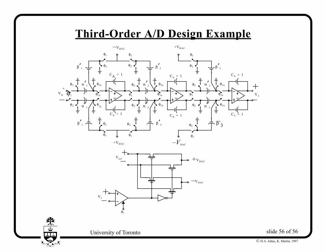
Third-Order A/D Design Example
φ2a
φ1a
φ1a
φ1a
+VDAC
+VDACVDAC–
V– DAC
φ2a
φ2a
φ1a
φ2a
φ2a
φ1
φ2
φ2
φ1
φ2
φ2
φ1
φ2
φ2
φ1 φ1
φ2
φ2
φ1
φ1
φ2
φ2
φ1
φ2
α′1
α′1
α′2
α′2
α′3
α′3
CA 1=
CA 1=
CA 1=
CA 1=
CA 1=
CA 1=
β′3
β′3
β′2
β′2
β′1
β′1
+Vin
–+
V3–
+V3–
φ1
+Vref– +VDAC
V– DAC
φ1
φ2