15. advanced laboratories - ttu.ee teaching/resource files/docs... · been described, this chapter...
TRANSCRIPT
www.msp430.ubi.pt Copyright 2009 Texas Instruments, All Rights Reserved 15-1
Chapter 15
15. Advanced Laboratories
Now that all the functions and features of the MSP430 devices have been described, this chapter presents several advanced laboratories that bring together many of the subjects discussed.
The first advanced laboratory consists of a new approach to teaching robotics, making use of the MSP430. It consists of the substitution of RoboSapien (RS) control and regulation electronics by the MSP430. The MSP430 replicates the RS operation, illustrating the capabilities of this microcontroller and as a way to motivate students.
The second advanced laboratory focuses on the MSP430 communications peripherals. It consists of developing an eZ430-RF2500 communication application to show how these communications peripherals are configured in a practical application. The aim of this laboratory is to use some of these hardware development tools to communicate together, activating their LEDs in response to writing messages to the Code Composer Essentials (CCE) console.
The third laboratory consists of a MSP430 assembly language tutorial. It includes examples using the different addressing modes and instructions format. It provides an overview of the fundamental characteristics of the assembly language instructions. It finishes with an assembly language project example: square root extraction with the CCE.
Topic Page
15.1 Lab11a. RoboSapien powered by MSP430 .....................15-3
15.1.1 What is RoboSapien?............................................15-3
15.1.2 How RoboSapien works? ......................................15-7
15.1.3 MSP430 integration............................................15-19
15.1.4 MSP430 C code programming.............................15-25
15.1.5 Tests and development of new functionalities ...15-31
15.1.6 Acknowledgments..............................................15-31
15.2 Lab11b. RF link with eZ430-RF2500 ............................15-32
Advanced Laboratories
15-2 Copyright 2009 Texas Instruments, All Rights Reserved www.msp430.ubi.pt
15.2.1 Introduction....................................................... 15-32
15.2.2 The application .................................................. 15-32
15.2.3 The hardware..................................................... 15-34
15.2.4 The software...................................................... 15-35
15.2.5 New Challenges ................................................. 15-41
15.3 Lab 11c. MSP430 assembly language tutorial.............. 15-42
15.3.1 Exploring the addressing modes of the MSP430 architecture .................................................................... 15-42
15.3.2 Exploring the addressing modes of the MSP430X CPU architecture .................................................................... 15-62
15.3.3 Assembly programming characteristics ............. 15-91
15.3.4 Creating an Assembly project with CCE............ 15-121
Lab11a. RoboSapien powered by MSP430
www.msp430.ubi.pt Copyright 2009 Texas Instruments, All Rights Reserved 15-3
15.1 Lab11a. RoboSapien powered by MSP430
Robotics is being increasingly used a vehicle for motivating students to learn embedded systems, artificial intelligence, computer science, and even general science and engineering. Typically, the laboratory classes of robotics courses involve the construction and programming of simple robots, usually composed of a microcontroller, sensors, device for remote communication and DC or stepper motors, mounted in all type of robot bodies.
Robotics involves both mechanical and electronic concepts, the latter requiring both hardware and software development for a specific application.
This advanced laboratory integrates together some multidisciplinary topics from different knowledge areas:
Control systems, for the different control approaches;
Embedded systems based on the MSP430;
Instrumentation and Measurements for the sensor signal conditioning and data acquisition;
C/C++ programming.
The objective of this advanced laboratory is to use a large number of the peripherals included in the MSP430, to test their capabilities in terms of memory and processing time and to perform a complex application such as driving the RS.
15.1.1 What is RoboSapien?
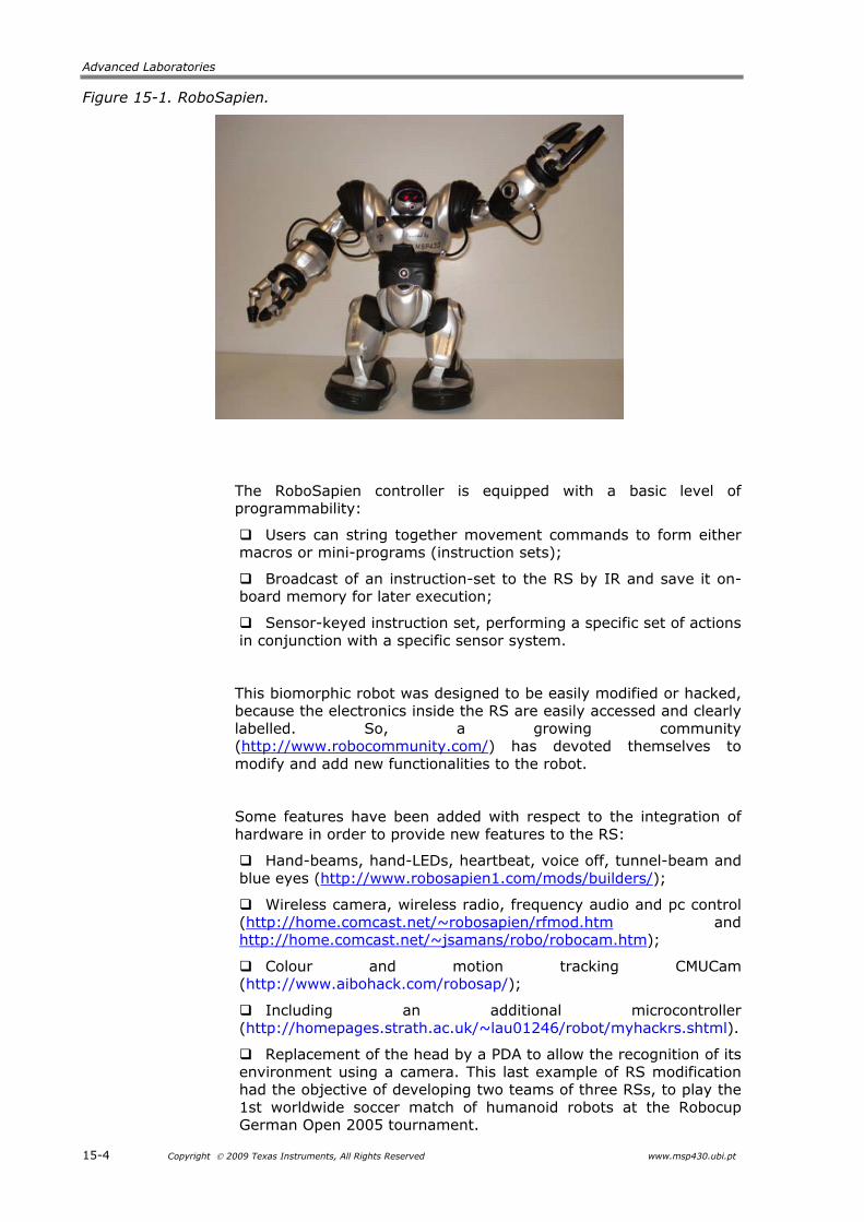
The RoboSapien (see Figure 15-1) is a humanoid robot designed by Mark W. Tilden, marketed by WowWee (www.wowwee.com/) for the toy market. Nowadays they provide many more robot products such as roboreptiles, roboraptors, robopets, among others. The RoboSapien measures approximately 34 cm in height and its weight is about 2.1 kg, including four mono (D) type batteries located in its feet.
Some words from the Robot Tech Support, from WowWee Ltd.:
“The RoboSapien is designed for modification. Here is the short hint list for the budding RS hacker.
First off, we must warn you that completely replacing the RS brain should only be attempted by those with a lot of time, electronic skills, and programming ego.
You don’t have to though — if you carefully remove the connectors and lift the RS motherboard, on the back you will find all inputs and outputs labeled, and right next to gold pads convenient for soldering wires...”
in http://www.robosapien1.com/resources/official-mod-guide/
Advanced Laboratories
15-4 Copyright 2009 Texas Instruments, All Rights Reserved www.msp430.ubi.pt
Figure 15-1. RoboSapien.
The RoboSapien controller is equipped with a basic level of programmability:
Users can string together movement commands to form either macros or mini-programs (instruction sets);
Broadcast of an instruction-set to the RS by IR and save it on-board memory for later execution;
Sensor-keyed instruction set, performing a specific set of actions in conjunction with a specific sensor system.
This biomorphic robot was designed to be easily modified or hacked, because the electronics inside the RS are easily accessed and clearly labelled. So, a growing community (http://www.robocommunity.com/) has devoted themselves to modify and add new functionalities to the robot.
Some features have been added with respect to the integration of hardware in order to provide new features to the RS:
Hand-beams, hand-LEDs, heartbeat, voice off, tunnel-beam and blue eyes (http://www.robosapien1.com/mods/builders/);
Wireless camera, wireless radio, frequency audio and pc control (http://home.comcast.net/~robosapien/rfmod.htm and http://home.comcast.net/~jsamans/robo/robocam.htm);
Colour and motion tracking CMUCam (http://www.aibohack.com/robosap/);
Including an additional microcontroller (http://homepages.strath.ac.uk/~lau01246/robot/myhackrs.shtml).
Replacement of the head by a PDA to allow the recognition of its environment using a camera. This last example of RS modification had the objective of developing two teams of three RSs, to play the 1st worldwide soccer match of humanoid robots at the Robocup German Open 2005 tournament.
Lab11a. RoboSapien powered by MSP430
www.msp430.ubi.pt Copyright 2009 Texas Instruments, All Rights Reserved 15-5
Search the Internet for additional information concerning modifications to the RS.
However, none of the active modifications discussed above involve substitution of the original controller.
This laboratory substitutes the RS’s ASIC with the MSP430, in order to replicate its original functions.
This laboratory begins with a dissection of the RS. In order to replace the original controller by the MSP430, it is fundamental to analyse all the input and output signals of the original controller for all the RS’s movements. This requires the use of an oscilloscope and a logic analyzer.
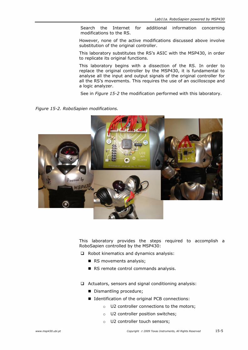
See in Figure 15-2 the modification performed with this laboratory.
Figure 15-2. RoboSapien modifications.
This laboratory provides the steps required to accomplish a RoboSapien controlled by the MSP430:
Robot kinematics and dynamics analysis:
RS movements analysis;
RS remote control commands analysis.
Actuators, sensors and signal conditioning analysis:
Dismantling procedure;
Identification of the original PCB connections:
o U2 controller connections to the motors;
o U2 controller position switches;
o U2 controller touch sensors;

Advanced Laboratories
15-6 Copyright 2009 Texas Instruments, All Rights Reserved www.msp430.ubi.pt
o U2 controller LEDs;
o U2 controller power and commands;
o U3 motor driver (H-bridge chip).
List and analysis of the function of all components and devices included in the original PCB;
List and analysis of the mechanical and/or electrical characteristics of the actuators, sensors and output devices;
Digital ports signals (motors) acquisition (using an oscilloscope and logic analyzer) and analysis:
Single movements;
Combined movements;
Motors active/inactive timetables corresponding to each movement.
Digital port signals (LEDs) acquisition (using an oscilloscope and logic analyzer) and analysis:
Determination of the eye pattern for each movement;
Active/inactive LEDs table corresponding to each movement.
IR commands acquisition (logic analyzer) and analysis:
Determination of the IR command digital value of each movement command of the remote control.
MSP430 integration:
Fabrication and assembly of the components and devices on the proposed MSP430 PCB;
Original controller removal;
Pin connections (soldering wires) from the MSP430 PCB to the RoboSapien PCB.
MSP430 C code programming (based on the data obtained from the previous steps):
Define the motors active/inactive timetables corresponding to each movement (movement tables);
Define the active/inactive LEDs output port pin values corresponding to each movement;
Define the IR digital input value of each movement command of the remote control.
At the end of this laboratory, it will be possible to integrate new features to the RoboSapien based on the resources provided by the MSP430.
Lab11a. RoboSapien powered by MSP430
www.msp430.ubi.pt Copyright 2009 Texas Instruments, All Rights Reserved 15-7
15.1.2 How RoboSapien works?
The RS is commercially available. It can be found on the manufacturer’s web page or at several retailers.
Step 1: Robot kinematics and dynamics analysis
The first task consists in the analysis of the robot kinematics and dynamics (evaluation of the robot movements and its characteristics). This task requires testing the RS movements.
A. RS movements analysis
The evaluation of the RS dynamics has shown that due to its low centre of mass, it is very stable.
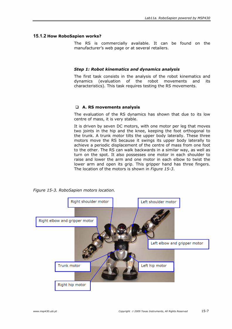
It is driven by seven DC motors, with one motor per leg that moves two joints in the hip and the knee, keeping the foot orthogonal to the trunk. A trunk motor tilts the upper body laterally. These three motors move the RS because it swings its upper body laterally to achieve a periodic displacement of the centre of mass from one foot to the other. The RS can walk backwards in a similar way, as well as turn on the spot. It also possesses one motor in each shoulder to raise and lower the arm and one motor in each elbow to twist the lower arm and open its grip. This gripper hand has three fingers. The location of the motors is shown in Figure 15-3.
Figure 15-3. RoboSapien motors location.
Advanced Laboratories
15-8 Copyright 2009 Texas Instruments, All Rights Reserved www.msp430.ubi.pt
The dynamic walking pattern of RS follows the following sequence:
(1) The trunk motor tilts the upper body to the right. The centre of mass shifts over the right foot. The left foot lifts from the ground;
(2) The hip motors move in opposite directions, resulting in a forward motion of the robot. As the upper body swings back, the left foot regains contact with the ground;
(3) Symmetrical to (1). The trunk motor tilts the body to left;
(4) Symmetrical to (2).
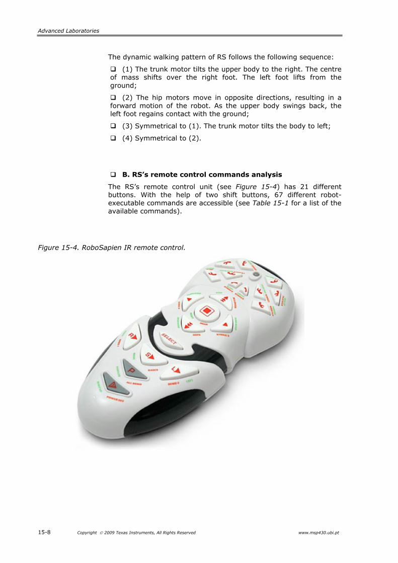
B. RS’s remote control commands analysis
The RS’s remote control unit (see Figure 15-4) has 21 different buttons. With the help of two shift buttons, 67 different robot-executable commands are accessible (see Table 15-1 for a list of the available commands).
Figure 15-4. RoboSapien IR remote control.

Lab11a. RoboSapien powered by MSP430
www.msp430.ubi.pt Copyright 2009 Texas Instruments, All Rights Reserved 15-9
Table 15-1. Movement commands.
Commands (no shift) GREEN shift commands ORANGE shift commands turn right right turn step right hand strike 3
right arm up right hand thump right hand sweep right arm out right hand throw Burp tilt body right sleep right hand strike 2
right arm down right hand pickup high 5 right arm in lean backwards right hand strike 1
walk forwards forward step bulldozer walk backwards backward step oops (fart)
turn left left turn step left hand strike 3 left arm up left hand thump left hand sweep left arm out left hand throw Whistle tilt body left listen left hand strike 2
left arm down left hand pick up talk back left arm in lean forward left hand strike 1
stop reset Roar Execute (master command program) All Demo Wakeup Power Off Right (right sensor program) Demo 1 (Karate skits) Left (left sensor program) Demo 2 (Rude skits) Sonic (sonic sensor program) Dance
*There are also some secret undocumented codes.
Step 2: Actuators, sensors and signal conditioning analysis
The next task requires a dismantling procedure to be followed to allow the detailed analysis of the actuators (motors) and regulation electronics, sensors and respective signal conditioning, and of the PCB included in the original robot.
See http://personal.strath.ac.uk/mark.craig/robot/robos.shtml for a procedure to dismantle the RS in order to give it additional features.
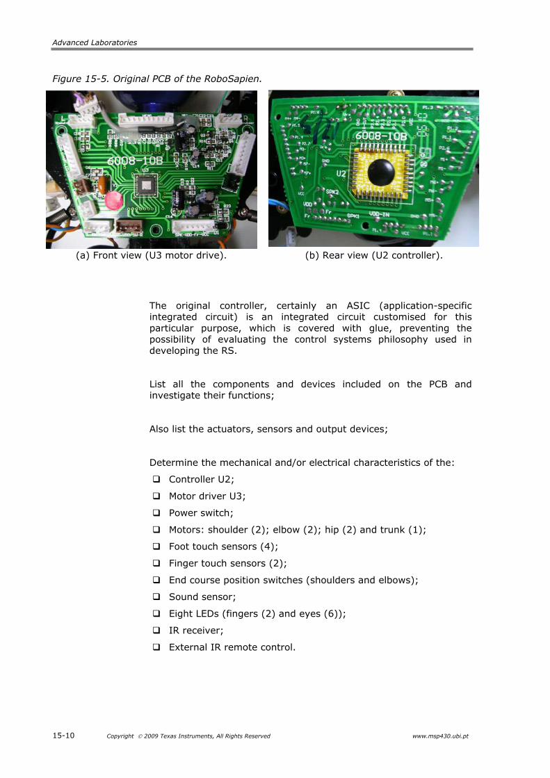
As shown, the RS’s PCB (Controller U2 and Motor Driver U3) is easily accessed and clearly labelled, indicating the:
Motors (M);
Input or output port (P);
Raw battery voltage that fluctuates wildly (VDD);
Regulated voltage (Vcc = 3.6V);
Universal ground (Gnd).
This task requires the identification all the connections of the PCB shown in Figure 15-5.
Advanced Laboratories
15-10 Copyright 2009 Texas Instruments, All Rights Reserved www.msp430.ubi.pt
Figure 15-5. Original PCB of the RoboSapien.
(a) Front view (U3 motor drive). (b) Rear view (U2 controller).
The original controller, certainly an ASIC (application-specific integrated circuit) is an integrated circuit customised for this particular purpose, which is covered with glue, preventing the possibility of evaluating the control systems philosophy used in developing the RS.
List all the components and devices included on the PCB and investigate their functions;
Also list the actuators, sensors and output devices;
Determine the mechanical and/or electrical characteristics of the:
Controller U2;
Motor driver U3;
Power switch;
Motors: shoulder (2); elbow (2); hip (2) and trunk (1);
Foot touch sensors (4);
Finger touch sensors (2);
End course position switches (shoulders and elbows);
Sound sensor;
Eight LEDs (fingers (2) and eyes (6));
IR receiver;
External IR remote control.

Lab11a. RoboSapien powered by MSP430
www.msp430.ubi.pt Copyright 2009 Texas Instruments, All Rights Reserved 15-11
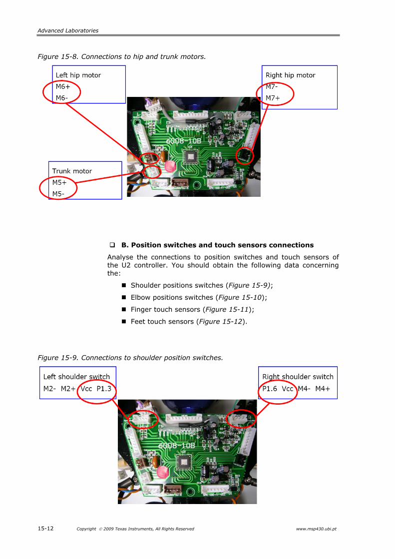
A. Motor controller (U2) connections
Analyse the connections to the motors of the U2 controller. You should obtain the following data concerning the:
Shoulder motors (Figure 15-6);
Elbow motors (Figure 15-7);
Hip and trunk motors (Figure 15-8).
Figure 15-6. Connections to shoulder motors.
Figure 15-7. Connections to elbow motors.
Advanced Laboratories
15-12 Copyright 2009 Texas Instruments, All Rights Reserved www.msp430.ubi.pt
Figure 15-8. Connections to hip and trunk motors.
B. Position switches and touch sensors connections
Analyse the connections to position switches and touch sensors of the U2 controller. You should obtain the following data concerning the:
Shoulder positions switches (Figure 15-9);
Elbow positions switches (Figure 15-10);
Finger touch sensors (Figure 15-11);
Feet touch sensors (Figure 15-12).
Figure 15-9. Connections to shoulder position switches.

Lab11a. RoboSapien powered by MSP430
www.msp430.ubi.pt Copyright 2009 Texas Instruments, All Rights Reserved 15-13
Figure 15-10. Connections to elbow position switches.
Figure 15-11. Connections to finger touch sensors.
Figure 15-12. Connections to feet touch sensors.

Advanced Laboratories
15-14 Copyright 2009 Texas Instruments, All Rights Reserved www.msp430.ubi.pt
C. Connections to LEDs
Analyse the LED connections of the U2 controller. You should obtain the following data concerning the:
Finger LEDs (Figure 15-13);
Eye LEDs (Figure 15-14).
Figure 15-13. Connections to finger LEDs.
Figure 15-14. Connections to eye LEDs.

Lab11a. RoboSapien powered by MSP430
www.msp430.ubi.pt Copyright 2009 Texas Instruments, All Rights Reserved 15-15
D. Command and power connections
Analyse the command and power connections of the U2 controller. You should obtain the data shown in Figure 15-15.
Figure 15-15. Command and power connections.
E. Digital ports signal acquisition and analysis
After obtaining the information with respect to the U2 controller connections on the PCB, proceed with the analysis of the digital signals acquired from the electronic board ports.
The aim of this task is to evaluate the original controller control output ports when the robot performs a specific command function. All the executable commands are available in the robot user’s guide or on the web pages previously mentioned.
This task is required to evaluate the state of each of U2’s output ports for control of the motors, in order to define the time sequence of active/inactive motors for each specific movement.
The procedure consists of measuring the ports digital signals, initially for a single motor movement, and then to command functions that combine several movements at the same time, listing the time that each motor is active and inactive.
Advanced Laboratories
15-16 Copyright 2009 Texas Instruments, All Rights Reserved www.msp430.ubi.pt
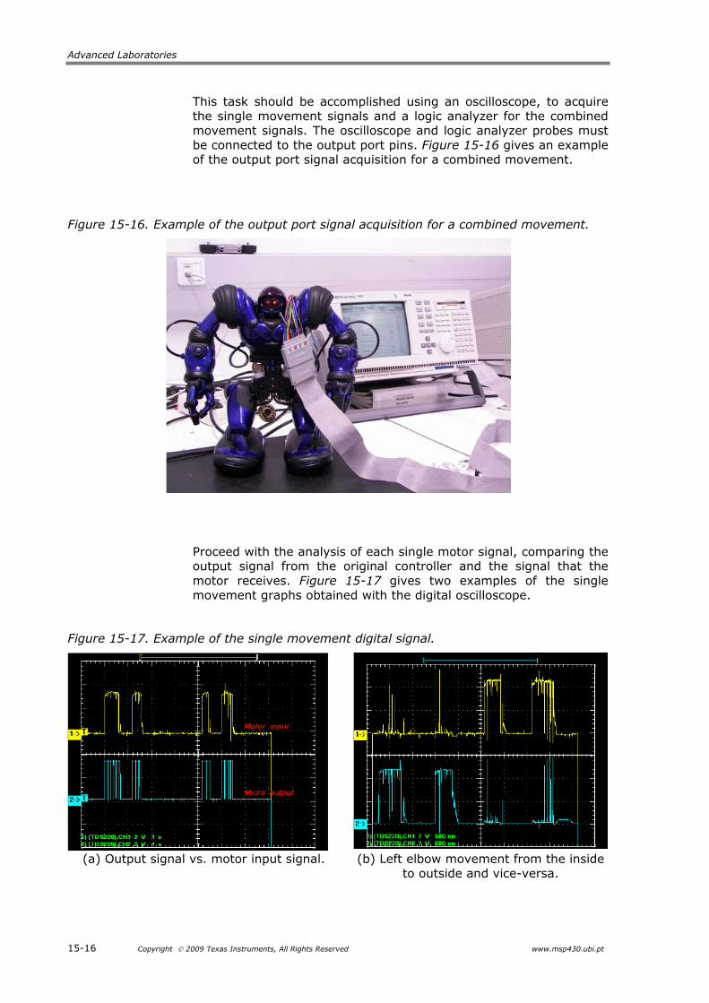
This task should be accomplished using an oscilloscope, to acquire the single movement signals and a logic analyzer for the combined movement signals. The oscilloscope and logic analyzer probes must be connected to the output port pins. Figure 15-16 gives an example of the output port signal acquisition for a combined movement.
Figure 15-16. Example of the output port signal acquisition for a combined movement.
Proceed with the analysis of each single motor signal, comparing the output signal from the original controller and the signal that the motor receives. Figure 15-17 gives two examples of the single movement graphs obtained with the digital oscilloscope.
Figure 15-17. Example of the single movement digital signal.
(a) Output signal vs. motor input signal. (b) Left elbow movement from the inside
to outside and vice-versa.

Lab11a. RoboSapien powered by MSP430
www.msp430.ubi.pt Copyright 2009 Texas Instruments, All Rights Reserved 15-17
The analysis of the combined action signals requires the connection of wires to the original controller ports to measure the combined movements digital signals with a logic analyzer.
The acquisition of the graphical digital signals from the controller motor ports must be performed for all the combined functions defined in the remote control.
The graphical functions need only to be obtained for one side (left) of the robot movements since other side (right) performs the same movements, but the motors operate in opposite directions.
Example: Output port signals acquisition of a combined movement: “Oops” (see Figure 15-18).
In this function, signal “M1+” (Left Elbow Out) is “high”, for 531 msec and the rest of the time (2125 msec) is “low” and signal “M3+” (Right Elbow Out) has the same signal, since both elbows execute the movement at the same time.
Figure 15-18. Example of the combined movement analysis: Output port signals acquisition of a combined movement: Function “Oops”.
The file main.c contains the tables for each motor active/inactive time periods for each RS movement.
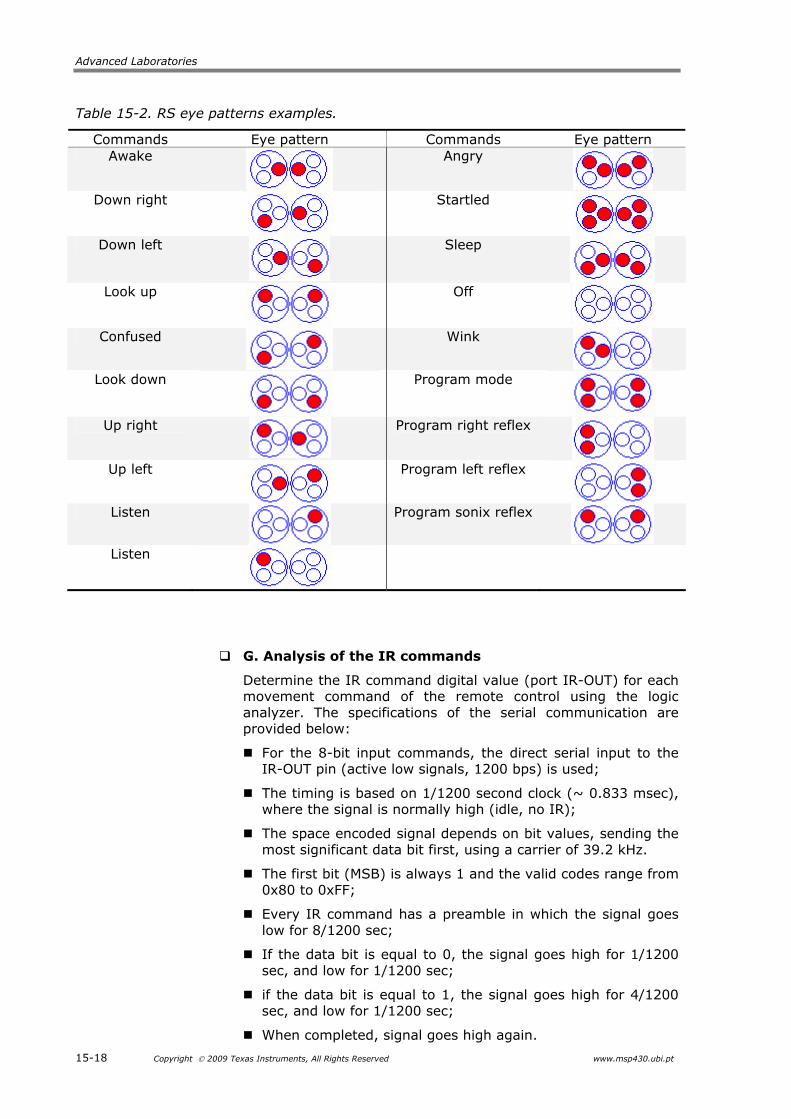
F. Eye patterns analysis
Evaluate the eye patterns (6 LEDs – P2.0 to P2.5) depending on the command that is executed;
The RS original controller has 3 outputs for each eye, presenting a distinct pattern for each condition;
This output condition can be used as an effective digital-level feedback source;
Table 15-2 gives some eye patterns, depending on the executed command.
Advanced Laboratories
15-18 Copyright 2009 Texas Instruments, All Rights Reserved www.msp430.ubi.pt
Table 15-2. RS eye patterns examples.
Commands Eye pattern Commands Eye pattern Awake
Angry
Down right
Startled
Down left
Sleep
Look up
Off
Confused
Wink
Look down
Program mode
Up right
Program right reflex
Up left
Program left reflex
Listen
Program sonix reflex
Listen
G. Analysis of the IR commands
Determine the IR command digital value (port IR-OUT) for each movement command of the remote control using the logic analyzer. The specifications of the serial communication are provided below:
For the 8-bit input commands, the direct serial input to the IR-OUT pin (active low signals, 1200 bps) is used;
The timing is based on 1/1200 second clock (~ 0.833 msec), where the signal is normally high (idle, no IR);
The space encoded signal depends on bit values, sending the most significant data bit first, using a carrier of 39.2 kHz.
The first bit (MSB) is always 1 and the valid codes range from 0x80 to 0xFF;
Every IR command has a preamble in which the signal goes low for 8/1200 sec;
If the data bit is equal to 0, the signal goes high for 1/1200 sec, and low for 1/1200 sec;
if the data bit is equal to 1, the signal goes high for 4/1200 sec, and low for 1/1200 sec;
When completed, signal goes high again.

Lab11a. RoboSapien powered by MSP430
www.msp430.ubi.pt Copyright 2009 Texas Instruments, All Rights Reserved 15-19
The file main.c contains all the digital IR values for all the commands.
Example: “Wake Up” IR command = 0xB1 (see Figure 15-19). (Find the complete description of the IR commands digital values on the web page: http://www.aibohack.com/robosap/ir_codes.htm).
Figure 15-19. Example of an IR command digital value: Function: “Wake Up”: 0xB1.
15.1.3 MSP430 integration
To replicate the RS operation, the MSP430F149 is used, making use of the following on-chip resources to control the RS:
Ports (output): P1.0 – P1.7 and P2.0 – P2.5 to drive the motors;
Ports (output): P5.0 – P5.7 to drive the LEDs;
Port (input): P4.0 for the IR signal;
Ports (input): P3.0 and P3.1 for the switches and touch sensors.
Figure 15-20 gives the PCB schematics that support the MSP430, connections to the RS PCB and other devices.
The detailed file of the schematics can be found in PCB_schematics.dxf.

Advanced Laboratories
15-20 Copyright 2009 Texas Instruments, All Rights Reserved www.msp430.ubi.pt
Figure 15-20. MSP430 PCB schematics developed to control the RoboSapien.
In this schematic, the connectors use the following port pin connections to the RS controller, as shown in Figure 15-23:
Table 15-3. New MSP430 PCB Connector Motors_1 connections to the RS controller.
‘F149 pin Motors1 pin U2 controller RS location Action P1.0 1 M1+ Left elbow Left arm out P1.1 2 M1- Left elbow Left arm in P1.2 3 M2+ Left shoulder Left arm up P1.3 4 M2- Left shoulder Left arm down P1.4 5 M3+ Right elbow Right arm out P1.5 6 M3- Right elbow Right arm in P1.6 7 M4+ Right shoulder Right arm up P1.7 8 M4- Right shoulder Right arm down
Lab11a. RoboSapien powered by MSP430
www.msp430.ubi.pt Copyright 2009 Texas Instruments, All Rights Reserved 15-21
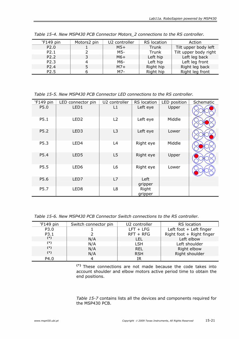
Table 15-4. New MSP430 PCB Connector Motors_2 connections to the RS controller.
‘F149 pin Motors2 pin U2 controller RS location Action P2.0 1 M5+ Trunk Tilt upper body left P2.1 2 M5- Trunk Tilt upper body right P2.2 3 M6+ Left hip Left leg back P2.3 4 M6- Left hip Left leg front P2.4 5 M7+ Right hip Right leg back P2.5 6 M7- Right hip Right leg front
Table 15-5. New MSP430 PCB Connector LED connections to the RS controller.
‘F149 pin LED connector pin U2 controller RS location LED position Schematic P5.0 LED1 L1 Left eye Upper
P5.1 LED2 L2 Left eye Middle
P5.2 LED3 L3 Left eye Lower
P5.3 LED4 L4 Right eye Middle
P5.4 LED5 L5 Right eye Upper
P5.5 LED6 L6 Right eye Lower
P5.6 LED7 L7 Left
gripper
P5.7 LED8 L8 Right gripper
Table 15-6. New MSP430 PCB Connector Switch connections to the RS controller.
‘F149 pin Switch connector pin U2 controller RS location P3.0 1 LFT + LFG Left foot + Left finger P3.1 2 RFT + RFG Right foot + Right finger
(*) N/A LEL Left elbow (*) N/A LSH Left shoulder (*) N/A REL Right elbow (*) N/A RSH Right shoulder
P4.0 4 IR
(*) These connections are not made because the code takes into account shoulder and elbow motors active period time to obtain the end positions.
Table 15-7 contains lists all the devices and components required for the MSP430 PCB.

Advanced Laboratories
15-22 Copyright 2009 Texas Instruments, All Rights Reserved www.msp430.ubi.pt
Table 15-7. Device and component list of the MSP430 PCB.
Description Designator Footprint LibRef Quant. Value Ref. Farnell: 7568533 C1 CR2012-0805 Cap 1 12 pF
Ref. Farnell: 7568533 C2 CR2012-0805 Cap 1 12 pF
Capacitor 0.1uF Ref Farnell: 317676 C3 CR2012-0805 Cap Semi 1 100 nF Capacitor, CASE A 10UF 6.3V Ref. Farnell: 967014 C4 CC3216-1206 Cap Pol1 1 10 uF
Capacitor 0.1uF Ref. Farnell: 317676 C5 CR2012-0805 Cap Semi 1 100 nF Capacitor, CASE A 10UF 6.3V Ref. Farnell: 967014 C6 CC3216-1206 Cap Pol1 1 10 uF
Ref. Farnell: 9406352 C15 CR2012-0805 Cap Semi 1 10 nF
Typical BLUE SiC LED DS1 LED LED3 1
Header, 7-Pin, Dual row P1 HDR2X7 Header 7X2 1
Ref. Farnell: 889477 + 9733051 P2 1.25MM2P Header 2 1
Ref. Farnell: 1012261 + 9733078 P3 1.25MM6P Header 6 1
Ref. Farnell:1012262 + 1012258 P4 1.25MM8P Header 8 1
Ref. Farnell: 9733116 + 9733060 P5 1.25MM4P Header 4 1
Ref. Farnell:1012262 + 1012258 P6 1.25MM8P Header 8 1
NPN General-purpose Transistor Q1 SOT23 BC847 1
NPN General-purpose Transistor Q2 SOT23 BC847 1
NPN General-purpose Transistor Q3 SOT23 BC847 1
NPN General-purpose Transistor Q4 SOT23 BC847 1
NPN General-purpose Transistor Q5 SOT23 BC847 1
NPN General-purpose Transistor Q6 SOT23 BC847 1
NPN General-purpose Transistor Q7 SOT23 BC847 1
NPN General-purpose Transistor Q8 SOT23 BC847 1
Resistor Farnell:1099812 R1 CR2012-0805 Res2 1 1K Resistor, 0805 330R Ref. Farnell: 1099797 R2 CR2012-0805 Res1 1 330R
Resistor R3 CR2012-0805 Res2 1 4K7
Resistor R4 CR2012-0805 Res2 1 4K7
Resistor R5 CR2012-0805 Res2 1 4K7
Resistor R6 CR2012-0805 Res2 1 4K7
Resistor R7 CR2012-0805 Res2 1 4K7
Resistor R8 CR2012-0805 Res2 1 4K7
Resistor R9 CR2012-0805 Res2 1 4K7
Resistor R10 CR2012-0805 Res2 1 4K7
Microcontroller uP1 PQFP64 MSP430F149 1
Surface Mount Quartz Crystal Y1 85SMX 85SMX 1 32 kHz
Figure 15-21 presents the PCB mask to integrate the MSP430. The detailed PCB mask (scale 1x1) can be found in file PCB_mask.dxf.

Lab11a. RoboSapien powered by MSP430
www.msp430.ubi.pt Copyright 2009 Texas Instruments, All Rights Reserved 15-23
Figure 15-21. MSP430 PCB mask.
This task requires the fabrication and assembly of the components and devices on the proposed PCB.
After this, proceed with the removal of the original controller from the RoboSapien PCB. It is recommended that if the connections that were hidden below the U2 controller are checked.
Figure 15-22 shows a detailed figure of the original PCB, without the ASIC.
Figure 15-22. RoboSapien PCB without U2 controller.
(a) RoboSapien PCB without controller. (b) Original ASIC.
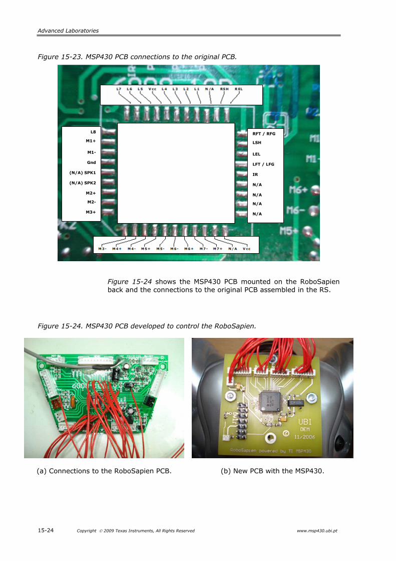
The next task requires soldering wires to the RoboSapien PCB to each pin location of the removed U2 controller. Figure 15-23 shows the MSP430 pins connections (connections P3 to P5 of Figure 15-20) to the original PCB.
Advanced Laboratories
15-24 Copyright 2009 Texas Instruments, All Rights Reserved www.msp430.ubi.pt
Figure 15-23. MSP430 PCB connections to the original PCB.
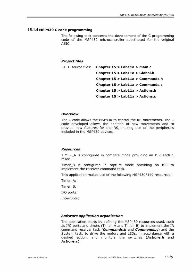
Figure 15-24 shows the MSP430 PCB mounted on the RoboSapien back and the connections to the original PCB assembled in the RS.
Figure 15-24. MSP430 PCB developed to control the RoboSapien.
(a) Connections to the RoboSapien PCB. (b) New PCB with the MSP430.
RFT / RFG
LSH
LEL
LFT / LFG
IR
N/A
N/A
N/A
N/A
L8
M1+
M1-
Gnd
(N/A) SPK1
(N/A) SPK2
M2+
M2-
M3+
Lab11a. RoboSapien powered by MSP430
www.msp430.ubi.pt Copyright 2009 Texas Instruments, All Rights Reserved 15-25
15.1.4 MSP430 C code programming
The following task concerns the development of the C programming code of the MSP430 microcontroller substituted for the original ASIC.
Project files
C source files: Chapter 15 > Lab11a > main.c
Chapter 15 > Lab11a > Global.h
Chapter 15 > Lab11a > Commands.h
Chapter 15 > Lab11a > Commands.c
Chapter 15 > Lab11a > Actions.h
Chapter 15 > Lab11a > Actions.c
Overview
The C code allows the MSP430 to control the RS movements. The C code developed allows the addition of new movements and to provide new features for the RS, making use of the peripherals included in the MSP430 devices.
Resources
TIMER_A is configured in compare mode providing an ISR each 1 msec.
Timer_B is configured in capture mode providing an ISR to implement the receiver command task.
This application makes use of the following MSP430F149 resources:
Timer_A;
Timer_B;
I/O ports;
Interrupts;
Software application organization
The application starts by defining the MSP430 resources used, such as I/O ports and timers (Timer_A and Timer_B) to implement the IR command receiver task (Commands.h and Commands.c) and the System task, to drive the motors and LEDs, in accordance with a desired action, and monitors the switches (Actions.h and Actions.c).

Advanced Laboratories
15-26 Copyright 2009 Texas Instruments, All Rights Reserved www.msp430.ubi.pt
The file main.c begins by reading the previous files and defining the movement tables “action data tables”. These tables contain the time to toggle each motor state (active/inactive), the LEDs patterns, the initial active motors and the enabled motors to provide the desired movement. The tables are constructed with the information collected in Step2E and Step2F.
Then, it defines the decoder tables containing the digital values of the IR commands (information collected in the Step2G).
The basic principles of the software are laid down in steps A to D:
A. Organization of the information concerning the RS actions
The information is organized as presented in Figure 15-25. The table pointers ensure rapid access to the “access table” information:
This table contains all the structure addresses containing the data for the RS movements;
The movements are defined in the data structures “data movements ()”;
This structure contains the time and sequence data for the operation of all motors, the initial state and the stop command;
Each motor starts at the initial state and toggles between states On and Off when the timer decreases to 0 (see Figure 15-26);
When counter reaches 0, the next timer is activated;
The motor stops if the counter reaches 0 and the next count contains zero.
Figure 15-25. Organization of the RoboSapien movement information.

Lab11a. RoboSapien powered by MSP430
www.msp430.ubi.pt Copyright 2009 Texas Instruments, All Rights Reserved 15-27
B. Logic motors
For the RS motors, there are 3 defined states:
Rotate clockwise;
Rotate counter clockwise;
Stop.
Each physical motor is implemented as two logical motors (see Figure 15-26).
Example: The physical motor M1 is represented by two logical motors M1+ and M1-, depending on the rotation direction.
If M1 = “state 0”, then M1+ = “High” and M1- = “Low”, consequently the physical motor M1 runs counter clockwise.
(Note: M1+ and M1- cannot have the same high state because in this case it will generate a short circuit).
Figure 15-26. Software operation principle.

Advanced Laboratories
15-28 Copyright 2009 Texas Instruments, All Rights Reserved www.msp430.ubi.pt
C. Command coding
The IR commands are decoded and the resulting command will cause a memory reload action, with the new data for the System Task function.
D. Motors activation function (System Task)
When the RS receives a new decoded command, it causes a memory load with the information for this new movement;
The function will act on this data stored in RAM;
The function counts the time, toggles the motors and LED states, and loads the new times until the movement ends;
This function is associated with a MSP430 counter and it is executed once every 1 msec;
This function also monitors the state of the emergency interrupts;
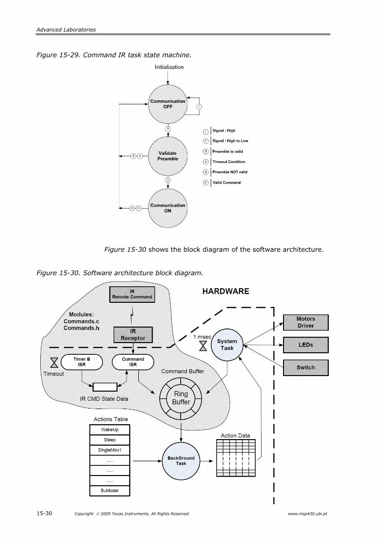
The C code is composed of several routines, each of which is dedicated to several tasks. In Figure 15-27 to Figure 15-29 are to be found Background and System tasks block diagrams and the IR task state machine.
Figure 15-27. Background task block diagram.

Lab11a. RoboSapien powered by MSP430
www.msp430.ubi.pt Copyright 2009 Texas Instruments, All Rights Reserved 15-29
Figure 15-28. System task block diagram.
Advanced Laboratories
15-30 Copyright 2009 Texas Instruments, All Rights Reserved www.msp430.ubi.pt
Figure 15-29. Command IR task state machine.
Figure 15-30 shows the block diagram of the software architecture.
Figure 15-30. Software architecture block diagram.
Lab11b. RF link with eZ430-RF2500
www.msp430.ubi.pt Copyright 2009 Texas Instruments, All Rights Reserved 15-31
15.1.5 Tests and development of new functionalities
The final task consists of performing tests to evaluate the robot movements and tuning slight discrepancies;
During this task, it is proposed to develop new functionalities because the substitution of the U2 controller by the MSP430 allows the RoboSapien to have an evolutionary capability, providing it with new features. Typical examples of these new features that you can develop are:
Substitution of the IR remote control commands by wireless communications using the eZ430-RF2500;
Expand computation capabilities using a powerful MSP430 device, in order to include features such as voice commands;
Integrate sensors (optical, acoustics and others...) and a digital camera to provide more autonomy to the RoboSapien.
Now, is up to you! Try to reach the next step of RoboSapien evolution.
15.1.6 Acknowledgments
This laboratory was developed with the help of Filipe Martins and Tiago Godinho, who developed this laboratory as the last year project for the undergraduate course of Electromechanical Engineering.
Advanced Laboratories
15-32 Copyright 2009 Texas Instruments, All Rights Reserved www.msp430.ubi.pt
15.2 Lab11b. RF link with eZ430-RF2500
15.2.1 Introduction
This laboratory demonstrates the operation of a small wireless communication application. It is an integrated project using some peripherals of the MSP430, in particular the USCIx communication modules. Additionally, it uses the CC2500 radio transceiver as an interface to external devices.
The application is characterized by its simplicity. However it is extremely motivating to students because it uses the IO console to allow easy interaction with the system. The implementation of this laboratory concerns sending and receiving text messages, making use of RF links between the central station (base station) and the various peripheral units (remote stations).
This laboratory seeks to achieve the following objectives:
Demonstrate the importance of the software organization as a fundamental part of an embedded systems project, making use of an initial approach to the problem in a top-down manner, with the necessary functional abstraction leading to the organization of the software by layers;
Exemplify the management of a complex project by integrating together more than one functional module.
Develop a modular arrangement that in practice leads to the coexistence of several functional modules in a single software project;
Exploit the wireless communications capability, demonstrating its practical advantages;
Consolidate knowledge acquired during the previous laboratories, namely, during the MSP430 communication interface laboratories, such as the SPI mode to access the CC2500 transceiver and the UART mode to interface to the IO console.
15.2.2 The application
The purpose of this laboratory is to establish communications between various RF stations. The stations are identified by an identifier (ID), that is, the address for presentation to the network. When a station wants to communicate with another station, it must give the address of the target station in the message.
The CC2500 has several ways to communicate, which affects the size of the exchanged messages. In order to simplify this procedure, it was decided to use the fixed size method for address + data (message maximum size of 64 Bytes). This corresponds to the size of CC2500 FIFO. Figure 15-31 below shows the format of the messages being exchanged.

Lab11b. RF link with eZ430-RF2500
www.msp430.ubi.pt Copyright 2009 Texas Instruments, All Rights Reserved 15-33
Figure 15-31. CC2500 packages format.
This laboratory has two stations with distinct functional behaviour and consequently differences in code. One assumes the base function and has the task of receiving messages from all peripheral stations, working as a radio beacon, sending acknowledge messages to all remote stations. Figure 15-32 illustrates this procedure.
Figure 15-32. Application block diagram.
Advanced Laboratories
15-34 Copyright 2009 Texas Instruments, All Rights Reserved www.msp430.ubi.pt
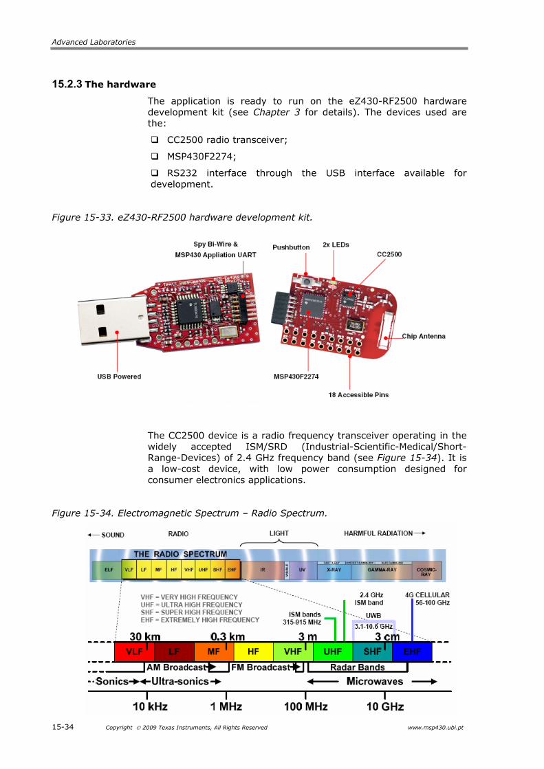
15.2.3 The hardware
The application is ready to run on the eZ430-RF2500 hardware development kit (see Chapter 3 for details). The devices used are the:
CC2500 radio transceiver;
MSP430F2274;
RS232 interface through the USB interface available for development.
Figure 15-33. eZ430-RF2500 hardware development kit.
The CC2500 device is a radio frequency transceiver operating in the widely accepted ISM/SRD (Industrial-Scientific-Medical/Short-Range-Devices) of 2.4 GHz frequency band (see Figure 15-34). It is a low-cost device, with low power consumption designed for consumer electronics applications.
Figure 15-34. Electromagnetic Spectrum – Radio Spectrum.

Lab11b. RF link with eZ430-RF2500
www.msp430.ubi.pt Copyright 2009 Texas Instruments, All Rights Reserved 15-35
The almost total absence of formatting protocol leaves the user to define their own communications protocol in software that best fits their needs.
The CC2500 is a low pin-out device, because it integrates all radio functions except the antenna (Figure 15-35). This device is not sufficiently independent so that it can operate without the aid of a microcontroller. When coupled to the MSP430, it makes the connection between them through SPI for access to the internal registers and uses two pins of GPIO to flag the operation status. In the particular case of the eZ430:
SPI interface belongs to the USCIB0 unit;
Status pins are the GDO0 and GDO2, connected to the Port2 pins P2.6 and P2.7 respectively.
Figure 15-35. CC2500 RF transceiver.
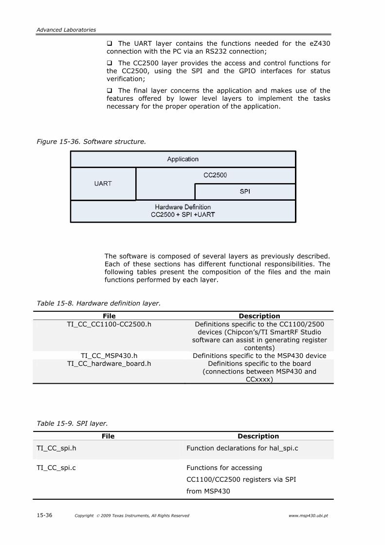
15.2.4 The software
Internal structure
The software is structured in layers and follows the structure shown in Figure 15-36:
At the base of the structure is the hardware abstraction layer, responsible for separating the higher layers software from the hardware;
The SPI layer is a middle layer that ensures the communication functions for the proper operation the CC2500;
Advanced Laboratories
15-36 Copyright 2009 Texas Instruments, All Rights Reserved www.msp430.ubi.pt
The UART layer contains the functions needed for the eZ430 connection with the PC via an RS232 connection;
The CC2500 layer provides the access and control functions for the CC2500, using the SPI and the GPIO interfaces for status verification;
The final layer concerns the application and makes use of the features offered by lower level layers to implement the tasks necessary for the proper operation of the application.
Figure 15-36. Software structure.
The software is composed of several layers as previously described. Each of these sections has different functional responsibilities. The following tables present the composition of the files and the main functions performed by each layer.
Table 15-8. Hardware definition layer.
File Description TI_CC_CC1100-CC2500.h Definitions specific to the CC1100/2500
devices (Chipcon’s/TI SmartRF Studio software can assist in generating register
contents) TI_CC_MSP430.h Definitions specific to the MSP430 device
TI_CC_hardware_board.h Definitions specific to the board (connections between MSP430 and
CCxxxx)
Table 15-9. SPI layer.
File Description
TI_CC_spi.h Function declarations for hal_spi.c
TI_CC_spi.c Functions for accessing
CC1100/CC2500 registers via SPI
from MSP430

Lab11b. RF link with eZ430-RF2500
www.msp430.ubi.pt Copyright 2009 Texas Instruments, All Rights Reserved 15-37
Table 15-10. CC2500 layer.
File Description
cc1100-CC2500.c Initialization of messages, transmission and reception functions.
TI_CC_CC1100-CC2500.h Function declarations for cc1100-CC2500.c
Table 15-11. UART layer.
File Description
hal_uart.c Initialization of messages and transmission functions via RS232.
hal_uart.h Function declarations for hal_uart.c
Configuration
Before the stations become operational, it is necessary to correctly start-up the multiple hardware modules, as well as the various software modules. Figure 15-37 shows this procedure. It is important to emphasize that the address of the stations need to be changed during compilation, to allocate the different addresses.
Figure 15-37. Station initialization algorithm.
START
Initialize MS 430 Interface
Power-Up reset signal sequence to CC2500
Write RF Settings to CC2500
Configure MSP430 IO
Put CC2500 in RX state
Enter Sleep mode 3
Set device Adress
Advanced Laboratories
15-38 Copyright 2009 Texas Instruments, All Rights Reserved www.msp430.ubi.pt
The functional distinction between the base and remote stations is achieved through the establishment of the BASE macro, which must be defined in order to build base station code.
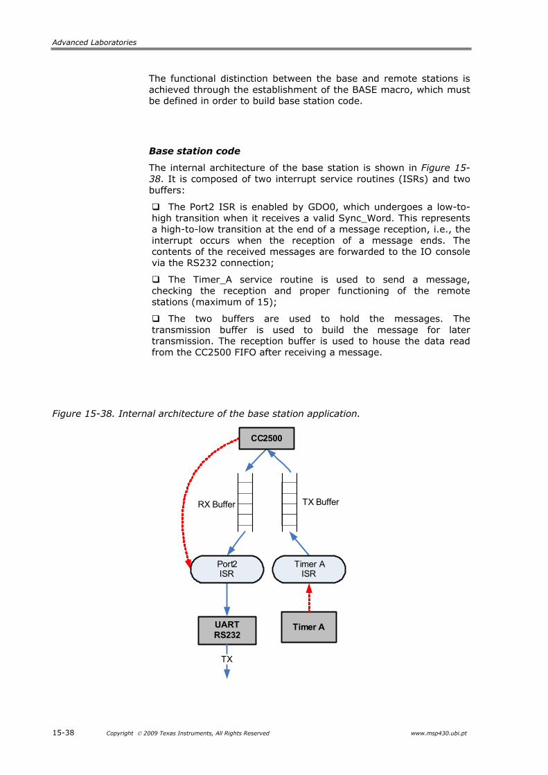
Base station code
The internal architecture of the base station is shown in Figure 15-38. It is composed of two interrupt service routines (ISRs) and two buffers:
The Port2 ISR is enabled by GDO0, which undergoes a low-to-high transition when it receives a valid Sync_Word. This represents a high-to-low transition at the end of a message reception, i.e., the interrupt occurs when the reception of a message ends. The contents of the received messages are forwarded to the IO console via the RS232 connection;
The Timer_A service routine is used to send a message, checking the reception and proper functioning of the remote stations (maximum of 15);
The two buffers are used to hold the messages. The transmission buffer is used to build the message for later transmission. The reception buffer is used to house the data read from the CC2500 FIFO after receiving a message.
Figure 15-38. Internal architecture of the base station application.
UARTRS232
Timer A
CC2500
TX BufferRX Buffer
Timer AISR
Port2ISR
TX

Lab11b. RF link with eZ430-RF2500
www.msp430.ubi.pt Copyright 2009 Texas Instruments, All Rights Reserved 15-39
Remote station code
The internal architecture of the base station is shown in Figure 15-39. It is composed of two interrupt service routines (ISR) and two buffers:
The Port2 ISR is enabled by the GDO0, which undergoes a low-to-high transition when it receives a valid Sync_Word. This represents a high-to-low transition at the end of reception of a message, i.e., the interrupt occurs when a message reception ends. The contents of the received messages are forwarded to the IO console via the RS232 connection.
The Port1 service routine is used to meet the demand caused by button pushes, sending the signal, which indicates the presence of the remote station;
The two buffers are used to hold the messages. The transmit buffer is used to build the message for later transmission. The receive buffer is used to house the data read from the CC2500 FIFO after receiving a message.
Figure 15-39. Internal architecture of the remote station application.
UARTRS232
KeyboardGPIO
CC2500
TX BufferRX Buffer
Port1RSI
Port2RSI
SwitchTX
Algorithms
The main algorithms of the application are the message receive and transmit:
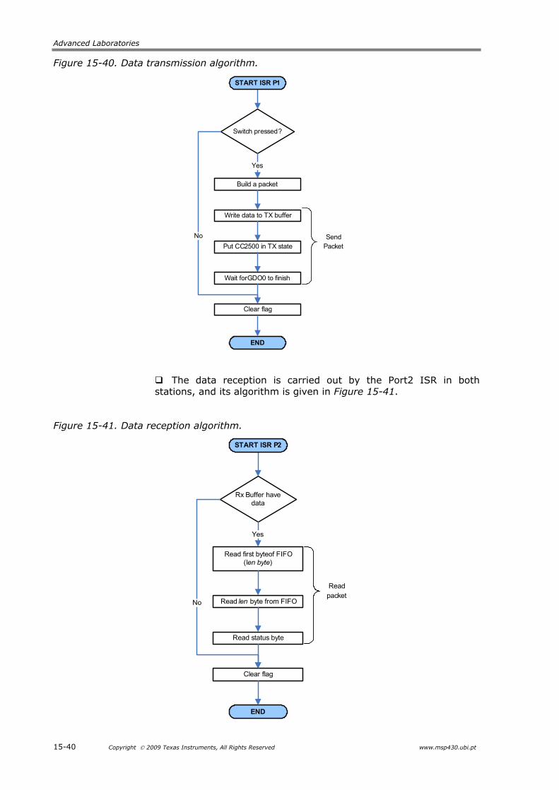
The data transmission algorithm implemented by the Port1 ISR is shown in Figure 15-40.
Advanced Laboratories
15-40 Copyright 2009 Texas Instruments, All Rights Reserved www.msp430.ubi.pt
Figure 15-40. Data transmission algorithm.
Switch pressed?
START ISR P1
Yes
Build a packet
Write data to TX buffer
Put CC2500 in TX state
Wait forGDO0 to finish
Clear flag
END
No Send Packet
The data reception is carried out by the Port2 ISR in both stations, and its algorithm is given in Figure 15-41.
Figure 15-41. Data reception algorithm.
Rx Buffer have data
START ISR P2
Yes
Read first byteof FIFO (len byte)
Read len byte from FIFO
Read status byte
Clear flag
END
No
Readpacket

Lab 11c. MSP430 assembly language tutorial
www.msp430.ubi.pt Copyright 2009 Texas Instruments, All Rights Reserved 15-41
15.2.5 New Challenges
Having understood the importance of this laboratory for bringing together the ideas and concepts taught in this CDROM, it is now the starting point for other and more exciting new challenges.
Starting with the present laboratory as a knowledge and technology base, develop an application to exchange written messages between the various stations scattered inside a room, a kind of "wireless messenger". The messages typed into the IO console and associated with an address would be sent by a wireless device to reach the console addressed. To achieve this objective, it is necessary to define a small command set available to the user, such as:
Address allocation to the local station;
Address allocation to the remote station;
Sending a message;
Neighbourhood screening of possible talk partners;
Among others…
Advanced Laboratories
15-42 Copyright 2009 Texas Instruments, All Rights Reserved www.msp430.ubi.pt
15.3 Lab 11c. MSP430 assembly language tutorial
15.3.1 Exploring the addressing modes of the MSP430 architecture
The MSP430 architecture
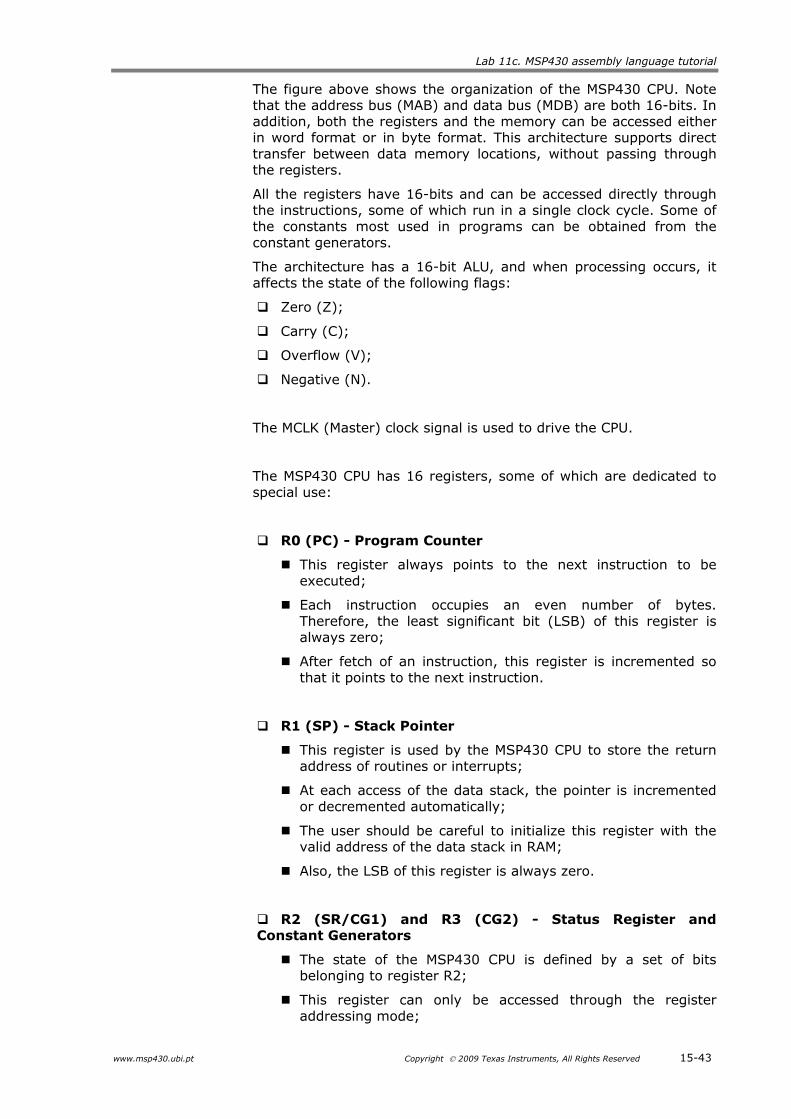
The MSP430 CPU incorporates features specifically designed to allow the use of modern programming techniques such as the computation of jump addresses, data processing in tables, and the use of high-level languages such as C. The whole memory space can be addressed by the MSP430 CPU using seven different addressing modes, without the need for paging. The MSP430 CPU has a set of 27 instructions that can be used with any of the addressing modes.
Figure 15-42. MSP430 CPU block diagram.
Lab 11c. MSP430 assembly language tutorial
www.msp430.ubi.pt Copyright 2009 Texas Instruments, All Rights Reserved 15-43
The figure above shows the organization of the MSP430 CPU. Note that the address bus (MAB) and data bus (MDB) are both 16-bits. In addition, both the registers and the memory can be accessed either in word format or in byte format. This architecture supports direct transfer between data memory locations, without passing through the registers.
All the registers have 16-bits and can be accessed directly through the instructions, some of which run in a single clock cycle. Some of the constants most used in programs can be obtained from the constant generators.
The architecture has a 16-bit ALU, and when processing occurs, it affects the state of the following flags:
Zero (Z);
Carry (C);
Overflow (V);
Negative (N).
The MCLK (Master) clock signal is used to drive the CPU.
The MSP430 CPU has 16 registers, some of which are dedicated to special use:
R0 (PC) - Program Counter
This register always points to the next instruction to be executed;
Each instruction occupies an even number of bytes. Therefore, the least significant bit (LSB) of this register is always zero;
After fetch of an instruction, this register is incremented so that it points to the next instruction.
R1 (SP) - Stack Pointer
This register is used by the MSP430 CPU to store the return address of routines or interrupts;
At each access of the data stack, the pointer is incremented or decremented automatically;
The user should be careful to initialize this register with the valid address of the data stack in RAM;
Also, the LSB of this register is always zero.
R2 (SR/CG1) and R3 (CG2) - Status Register and Constant Generators
The state of the MSP430 CPU is defined by a set of bits belonging to register R2;
This register can only be accessed through the register addressing mode;
Advanced Laboratories
15-44 Copyright 2009 Texas Instruments, All Rights Reserved www.msp430.ubi.pt
All other addressing modes are reserved to support the constant generator;
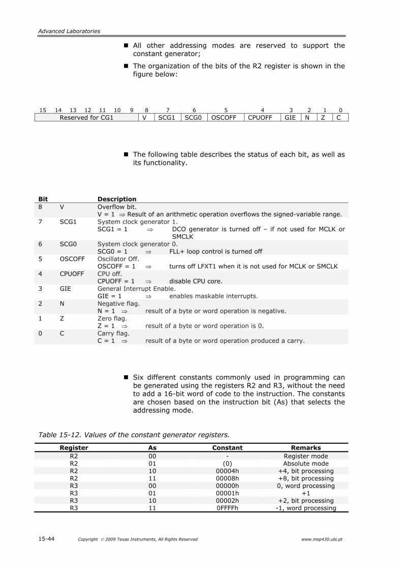
The organization of the bits of the R2 register is shown in the figure below:
15 14 13 12 11 10 9 8 7 6 5 4 3 2 1 0 Reserved for CG1 V SCG1 SCG0 OSCOFF CPUOFF GIE N Z C
The following table describes the status of each bit, as well as its functionality.
Bit Description 8 V Overflow bit.
V = 1 Result of an arithmetic operation overflows the signed-variable range. 7 SCG1 System clock generator 1.
SCG1 = 1 DCO generator is turned off – if not used for MCLK or SMCLK
6 SCG0 System clock generator 0. SCG0 = 1 FLL+ loop control is turned off
5 OSCOFF Oscillator Off. OSCOFF = 1 turns off LFXT1 when it is not used for MCLK or SMCLK
4 CPUOFF CPU off. CPUOFF = 1 disable CPU core.
3 GIE General Interrupt Enable. GIE = 1 enables maskable interrupts.
2 N Negative flag. N = 1 result of a byte or word operation is negative.
1 Z Zero flag. Z = 1 result of a byte or word operation is 0.
0 C Carry flag. C = 1 result of a byte or word operation produced a carry.
Six different constants commonly used in programming can be generated using the registers R2 and R3, without the need to add a 16-bit word of code to the instruction. The constants are chosen based on the instruction bit (As) that selects the addressing mode.
Table 15-12. Values of the constant generator registers.
Register As Constant Remarks R2 00 - Register mode R2 01 (0) Absolute mode R2 10 00004h +4, bit processing R2 11 00008h +8, bit processing R3 00 00000h 0, word processing R3 01 00001h +1 R3 10 00002h +2, bit processing R3 11 0FFFFh -1, word processing
Lab 11c. MSP430 assembly language tutorial
www.msp430.ubi.pt Copyright 2009 Texas Instruments, All Rights Reserved 15-45
Whenever the operand is one of the six constants, the registers are selected automatically. Therefore, R2 and R3 cannot be addressed explicitly in constant mode, as they act as source registers.
R4-R15 - General-purpose registers
The general purpose registers R4 to R15 can be used as data registers, data pointers or index registers and can be accessed either as a byte or as a word;
These registers support operations on words or bytes;
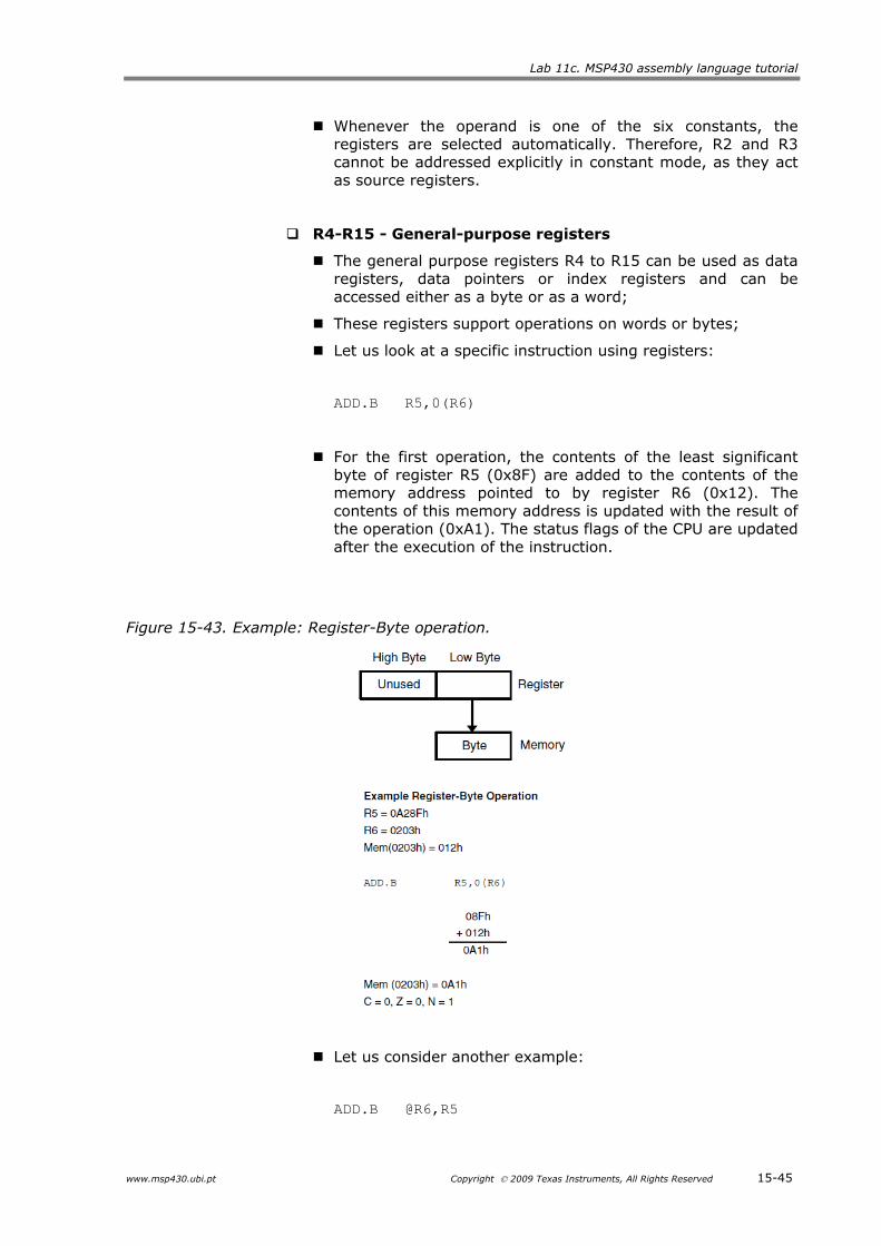
Let us look at a specific instruction using registers:
ADD.B R5,0(R6)
For the first operation, the contents of the least significant byte of register R5 (0x8F) are added to the contents of the memory address pointed to by register R6 (0x12). The contents of this memory address is updated with the result of the operation (0xA1). The status flags of the CPU are updated after the execution of the instruction.
Figure 15-43. Example: Register-Byte operation.
Let us consider another example:
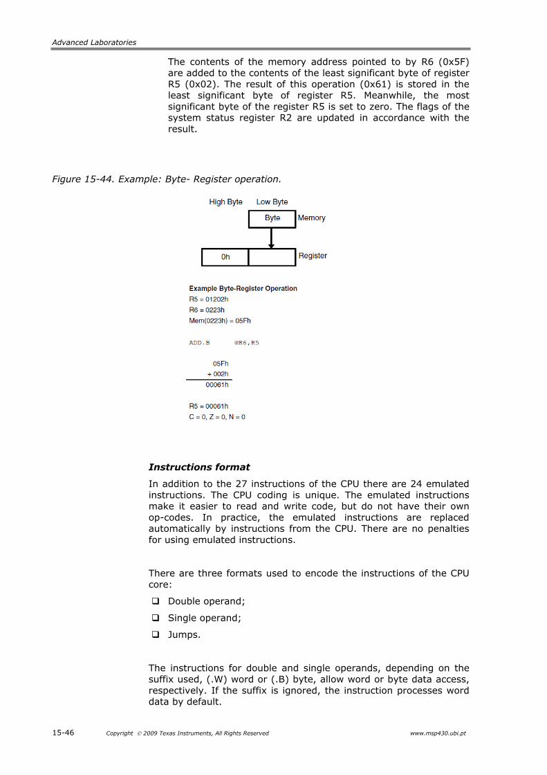
ADD.B @R6,R5
Advanced Laboratories
15-46 Copyright 2009 Texas Instruments, All Rights Reserved www.msp430.ubi.pt
The contents of the memory address pointed to by R6 (0x5F) are added to the contents of the least significant byte of register R5 (0x02). The result of this operation (0x61) is stored in the least significant byte of register R5. Meanwhile, the most significant byte of the register R5 is set to zero. The flags of the system status register R2 are updated in accordance with the result.
Figure 15-44. Example: Byte- Register operation.
Instructions format
In addition to the 27 instructions of the CPU there are 24 emulated instructions. The CPU coding is unique. The emulated instructions make it easier to read and write code, but do not have their own op-codes. In practice, the emulated instructions are replaced automatically by instructions from the CPU. There are no penalties for using emulated instructions.
There are three formats used to encode the instructions of the CPU core:
Double operand;
Single operand;
Jumps.
The instructions for double and single operands, depending on the suffix used, (.W) word or (.B) byte, allow word or byte data access, respectively. If the suffix is ignored, the instruction processes word data by default.
Lab 11c. MSP430 assembly language tutorial
www.msp430.ubi.pt Copyright 2009 Texas Instruments, All Rights Reserved 15-47
The source and destination of the data operated on by an instruction are defined by the following fields:
src: source operand addressing as defined in As and S-reg;
dst: destination operand addressing as defined in Ad and D-reg;
As: addressing bits used to define the addressing mode used by the source operand;
S-reg: register used by the source operand;
Ad: addressing bits used to define the addressing mode used by the destination operand;
D-reg: register used by destination operand;
B/W: word or byte accessing decision bit.
While all addresses within the address space are valid, it is the responsibility of the user to check the type of access that is used: for example, the contents of the flash memory can be used as a source operand, but can only be written to under certain conditions.
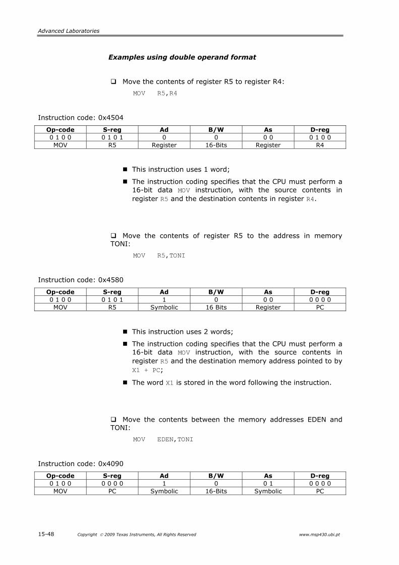
Instruction format I - double operand
The following figure shows the organization of instructions with two operands:
15 14 13 12 11 10 9 8 7 6 5 4 3 2 1 0 Op-code S-Reg Ad B/W As D-Reg
The following table shows the instructions that use this format.
Table 15-13. Double operand instructions.
Mnemonic Operation Description Arithmetic instructions ADD(.B or .W) src,dst src+dstdst Add source to destination ADDC(.B or .W) src,dst src+dst+Cdst Add source and carry to destination DADD(.B or .W) src,dst src+dst+Cdst (dec) Decimal add source and carry to destination SUB(.B or .W) src,dst dst+.not.src+1dst Subtract source from destination SUBC(.B or .W) src,dst dst+.not.src+Cdst Subtract source and not carry from
destination Logical and register control instructions AND(.B or .W) src,dst src.and.dstdst AND source with destination BIC(.B or .W) src,dst .not.src.and.dstdst Clear bits in destination BIS(.B or .W) src,dst src.or.dstdst Set bits in destination BIT(.B or .W) src,dst src.and.dst Test bits in destination XOR(.B or .W) src,dst src.xor.dstdst Exclusive OR (XOR) source with destination Data instructions CMP(.B or .W) src,dst dst-src Compare source with destination MOV(.B or .W) src,dst srcdst Move source to destination
The instructions CMP and SUB are identical, except for the way the result is stored. The same goes for the BIT and AND instructions.
Advanced Laboratories
15-48 Copyright 2009 Texas Instruments, All Rights Reserved www.msp430.ubi.pt
Examples using double operand format
Move the contents of register R5 to register R4:
MOV R5,R4
Instruction code: 0x4504
Op-code S-reg Ad B/W As D-reg 0 1 0 0 0 1 0 1 0 0 0 0 0 1 0 0 MOV R5 Register 16-Bits Register R4
This instruction uses 1 word;
The instruction coding specifies that the CPU must perform a 16-bit data MOV instruction, with the source contents in register R5 and the destination contents in register R4.
Move the contents of register R5 to the address in memory TONI:
MOV R5,TONI
Instruction code: 0x4580
Op-code S-reg Ad B/W As D-reg 0 1 0 0 0 1 0 1 1 0 0 0 0 0 0 0 MOV R5 Symbolic 16 Bits Register PC
This instruction uses 2 words;
The instruction coding specifies that the CPU must perform a 16-bit data MOV instruction, with the source contents in register R5 and the destination memory address pointed to by X1 + PC;
The word X1 is stored in the word following the instruction.
Move the contents between the memory addresses EDEN and TONI:
MOV EDEN,TONI
Instruction code: 0x4090
Op-code S-reg Ad B/W As D-reg 0 1 0 0 0 0 0 0 1 0 0 1 0 0 0 0 MOV PC Symbolic 16-Bits Symbolic PC

Lab 11c. MSP430 assembly language tutorial
www.msp430.ubi.pt Copyright 2009 Texas Instruments, All Rights Reserved 15-49
This instruction uses 3 words;
The instruction coding specifies that the CPU must perform a 16-bit data MOV instruction, with source contents of the EDEN memory address pointed to by X1 + PC to the TONI memory address pointed to by X2 + PC;
The X1 word followed by the word X2 are stored in the 2 words after the instruction.
Instruction format II - Single operand
The instructions with a single operand are coded using the structure described in the following figure:
15 14 13 12 11 10 9 8 7 6 5 4 3 2 1 0 Op-code B/W Ad D/S-Reg
The set of instructions that use this coding method is shown in the following table:
Table 15-14. Single operand instructions.
Mnemonic Operation Description Logical and register control instructions RRA(.B or .W) dst MSBMSB…LSBC Rotate destination right RRC(.B or .W) dst CMSB…LSBC Rotate destination right through (from)
carry SWPB( or .W) dst Swap bytes Swap bytes in destination SXT dst bit 7bit 8…bit 15 Sign extend destination PUSH(.B or .W) src SP-2SP, src@SP Push source on stack Program flow control instructions CALL(.B or .W) dst SP-2SP, PC+2@SP
dstPC Subroutine call to destination
RETI TOSSR, SP+2SP TOSPC, SP+2SP
Return from interrupt
The CALL instruction can be used with any addressing mode. The word following the instruction contains the routine address when the symbolic, immediate, absolute or indexed addressing modes are used.
Examples using single operand format
Rotate the contents of register R5 to the right with carry flag:
RRC R5
Advanced Laboratories
15-50 Copyright 2009 Texas Instruments, All Rights Reserved www.msp430.ubi.pt
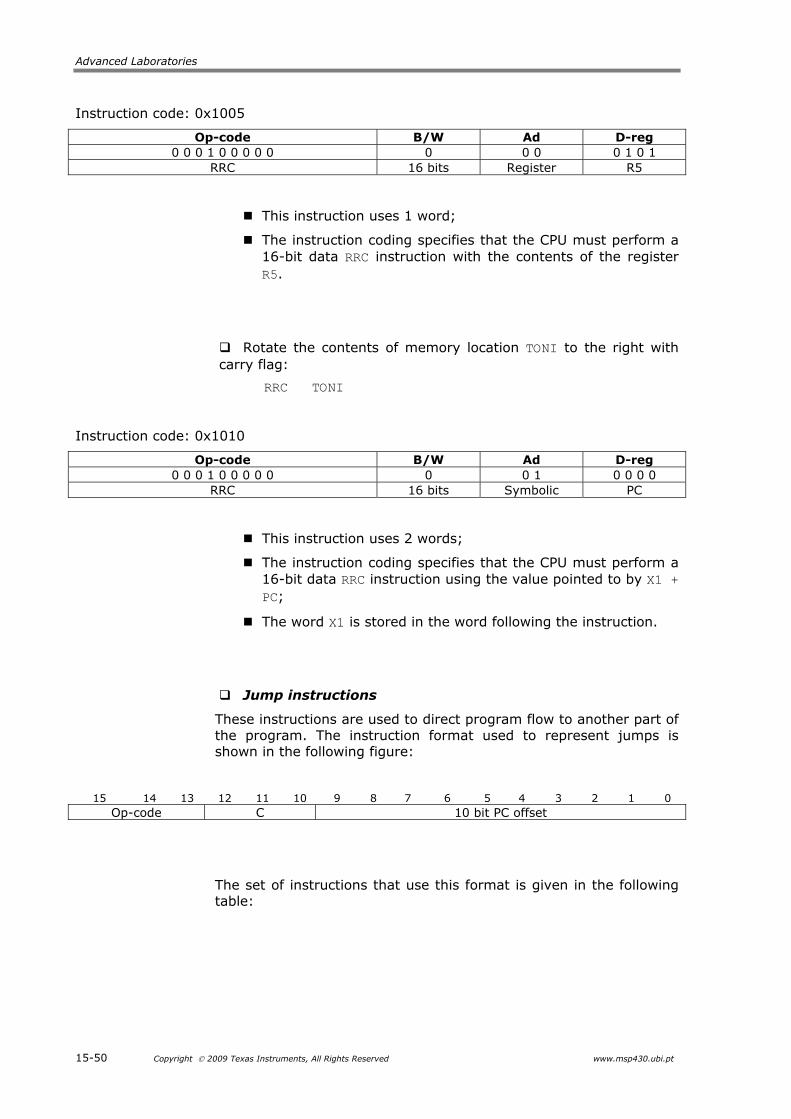
Instruction code: 0x1005
Op-code B/W Ad D-reg 0 0 0 1 0 0 0 0 0 0 0 0 0 1 0 1
RRC 16 bits Register R5
This instruction uses 1 word;
The instruction coding specifies that the CPU must perform a 16-bit data RRC instruction with the contents of the register R5.
Rotate the contents of memory location TONI to the right with carry flag:
RRC TONI
Instruction code: 0x1010
Op-code B/W Ad D-reg 0 0 0 1 0 0 0 0 0 0 0 1 0 0 0 0
RRC 16 bits Symbolic PC
This instruction uses 2 words;
The instruction coding specifies that the CPU must perform a 16-bit data RRC instruction using the value pointed to by X1 + PC;
The word X1 is stored in the word following the instruction.
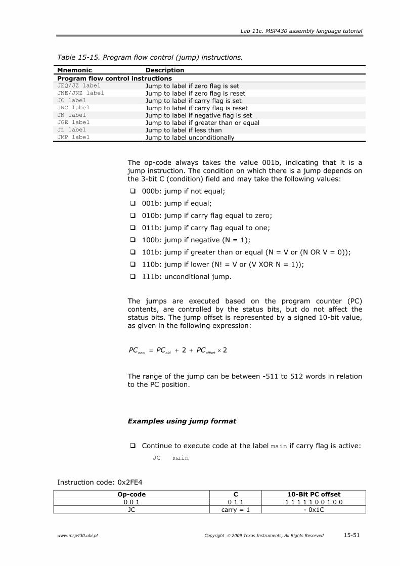
Jump instructions
These instructions are used to direct program flow to another part of the program. The instruction format used to represent jumps is shown in the following figure:
15 14 13 12 11 10 9 8 7 6 5 4 3 2 1 0 Op-code C 10 bit PC offset
The set of instructions that use this format is given in the following table:
Lab 11c. MSP430 assembly language tutorial
www.msp430.ubi.pt Copyright 2009 Texas Instruments, All Rights Reserved 15-51
Table 15-15. Program flow control (jump) instructions.
Mnemonic Description Program flow control instructions JEQ/JZ label Jump to label if zero flag is set JNE/JNZ label Jump to label if zero flag is reset JC label Jump to label if carry flag is set JNC label Jump to label if carry flag is reset JN label Jump to label if negative flag is set JGE label Jump to label if greater than or equal JL label Jump to label if less than JMP label Jump to label unconditionally
The op-code always takes the value 001b, indicating that it is a jump instruction. The condition on which there is a jump depends on the 3-bit C (condition) field and may take the following values:
000b: jump if not equal;
001b: jump if equal;
010b: jump if carry flag equal to zero;
011b: jump if carry flag equal to one;
100b: jump if negative (N = 1);
101b: jump if greater than or equal (N = V or (N OR V = 0));
110b: jump if lower (N! = V or (V XOR N = 1));
111b: unconditional jump.
The jumps are executed based on the program counter (PC) contents, are controlled by the status bits, but do not affect the status bits. The jump offset is represented by a signed 10-bit value, as given in the following expression:
22 offsetoldnew PCPCPC
The range of the jump can be between -511 to 512 words in relation to the PC position.
Examples using jump format
Continue to execute code at the label main if carry flag is active:
JC main
Instruction code: 0x2FE4
Op-code C 10-Bit PC offset 0 0 1 0 1 1 1 1 1 1 1 0 0 1 0 0
JC carry = 1 - 0x1C
Advanced Laboratories
15-52 Copyright 2009 Texas Instruments, All Rights Reserved www.msp430.ubi.pt
The instruction uses 1 word;
The instruction coding specifies that the PC must be loaded with the value resulting from the offset - 0x1C being applied to the previous expression.
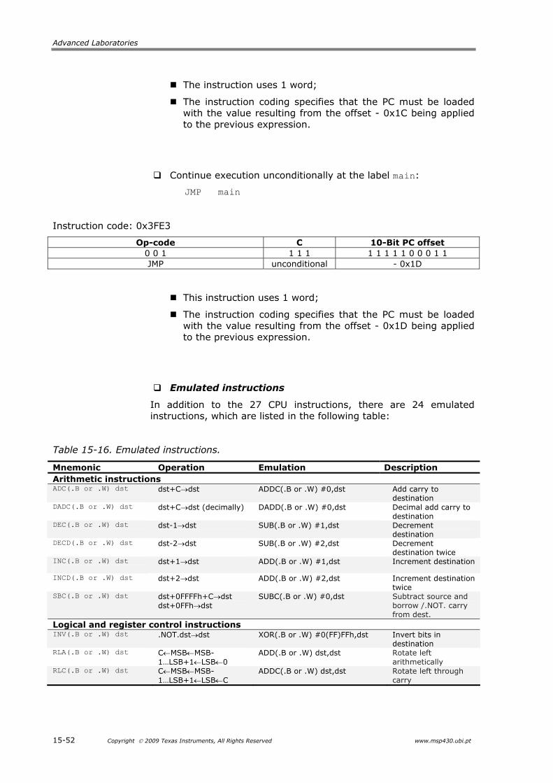
Continue execution unconditionally at the label main:
JMP main
Instruction code: 0x3FE3
Op-code C 10-Bit PC offset 0 0 1 1 1 1 1 1 1 1 1 0 0 0 1 1 JMP unconditional - 0x1D
This instruction uses 1 word;
The instruction coding specifies that the PC must be loaded with the value resulting from the offset - 0x1D being applied to the previous expression.
Emulated instructions
In addition to the 27 CPU instructions, there are 24 emulated instructions, which are listed in the following table:
Table 15-16. Emulated instructions.
Mnemonic Operation Emulation Description Arithmetic instructions ADC(.B or .W) dst dst+Cdst ADDC(.B or .W) #0,dst Add carry to
destination DADC(.B or .W) dst dst+Cdst (decimally) DADD(.B or .W) #0,dst Decimal add carry to
destination DEC(.B or .W) dst dst-1dst SUB(.B or .W) #1,dst Decrement
destination DECD(.B or .W) dst dst-2dst SUB(.B or .W) #2,dst Decrement
destination twice INC(.B or .W) dst
dst+1dst ADD(.B or .W) #1,dst Increment destination
INCD(.B or .W) dst dst+2dst ADD(.B or .W) #2,dst Increment destination twice
SBC(.B or .W) dst dst+0FFFFh+Cdst dst+0FFhdst
SUBC(.B or .W) #0,dst Subtract source and borrow /.NOT. carry from dest.
Logical and register control instructions INV(.B or .W) dst .NOT.dstdst XOR(.B or .W) #0(FF)FFh,dst Invert bits in
destination RLA(.B or .W) dst CMSBMSB-
1…LSB+1LSB0 ADD(.B or .W) dst,dst Rotate left
arithmetically RLC(.B or .W) dst CMSBMSB-
1…LSB+1LSBC ADDC(.B or .W) dst,dst Rotate left through
carry
Lab 11c. MSP430 assembly language tutorial
www.msp430.ubi.pt Copyright 2009 Texas Instruments, All Rights Reserved 15-53
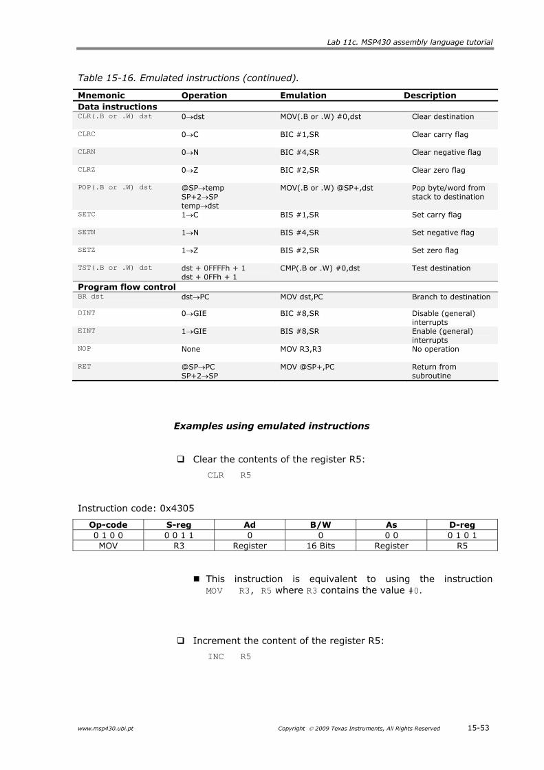
Table 15-16. Emulated instructions (continued).
Mnemonic Operation Emulation Description Data instructions CLR(.B or .W) dst 0dst MOV(.B or .W) #0,dst Clear destination
CLRC 0C BIC #1,SR Clear carry flag
CLRN 0N BIC #4,SR Clear negative flag
CLRZ 0Z BIC #2,SR Clear zero flag
POP(.B or .W) dst @SPtemp
SP+2SP tempdst
MOV(.B or .W) @SP+,dst Pop byte/word from stack to destination
SETC 1C BIS #1,SR Set carry flag
SETN 1N BIS #4,SR Set negative flag
SETZ 1Z BIS #2,SR Set zero flag
TST(.B or .W) dst dst + 0FFFFh + 1 dst + 0FFh + 1
CMP(.B or .W) #0,dst Test destination
Program flow control BR dst
dstPC MOV dst,PC Branch to destination
DINT 0GIE BIC #8,SR Disable (general) interrupts
EINT 1GIE BIS #8,SR Enable (general) interrupts
NOP None MOV R3,R3 No operation
RET @SPPC SP+2SP
MOV @SP+,PC Return from subroutine
Examples using emulated instructions
Clear the contents of the register R5:
CLR R5
Instruction code: 0x4305
Op-code S-reg Ad B/W As D-reg 0 1 0 0 0 0 1 1 0 0 0 0 0 1 0 1 MOV R3 Register 16 Bits Register R5
This instruction is equivalent to using the instruction MOV R3, R5 where R3 contains the value #0.
Increment the content of the register R5:
INC R5
Advanced Laboratories
15-54 Copyright 2009 Texas Instruments, All Rights Reserved www.msp430.ubi.pt
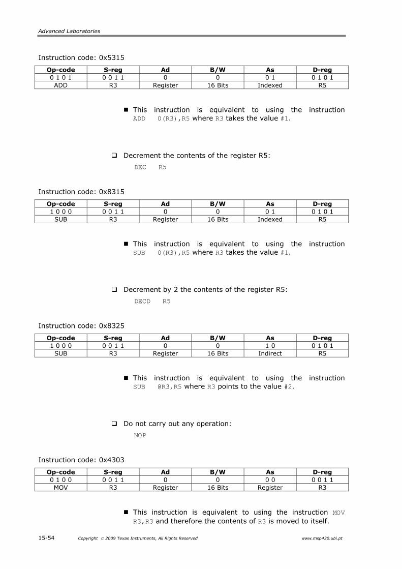
Instruction code: 0x5315
Op-code S-reg Ad B/W As D-reg 0 1 0 1 0 0 1 1 0 0 0 1 0 1 0 1 ADD R3 Register 16 Bits Indexed R5
This instruction is equivalent to using the instruction ADD 0(R3),R5 where R3 takes the value #1.
Decrement the contents of the register R5:
DEC R5
Instruction code: 0x8315
Op-code S-reg Ad B/W As D-reg 1 0 0 0 0 0 1 1 0 0 0 1 0 1 0 1
SUB R3 Register 16 Bits Indexed R5
This instruction is equivalent to using the instruction SUB 0(R3),R5 where R3 takes the value #1.
Decrement by 2 the contents of the register R5:
DECD R5
Instruction code: 0x8325
Op-code S-reg Ad B/W As D-reg 1 0 0 0 0 0 1 1 0 0 1 0 0 1 0 1
SUB R3 Register 16 Bits Indirect R5
This instruction is equivalent to using the instruction SUB @R3,R5 where R3 points to the value #2.
Do not carry out any operation:
NOP
Instruction code: 0x4303
Op-code S-reg Ad B/W As D-reg 0 1 0 0 0 0 1 1 0 0 0 0 0 0 1 1 MOV R3 Register 16 Bits Register R3
This instruction is equivalent to using the instruction MOV R3,R3 and therefore the contents of R3 is moved to itself.
Lab 11c. MSP430 assembly language tutorial
www.msp430.ubi.pt Copyright 2009 Texas Instruments, All Rights Reserved 15-55
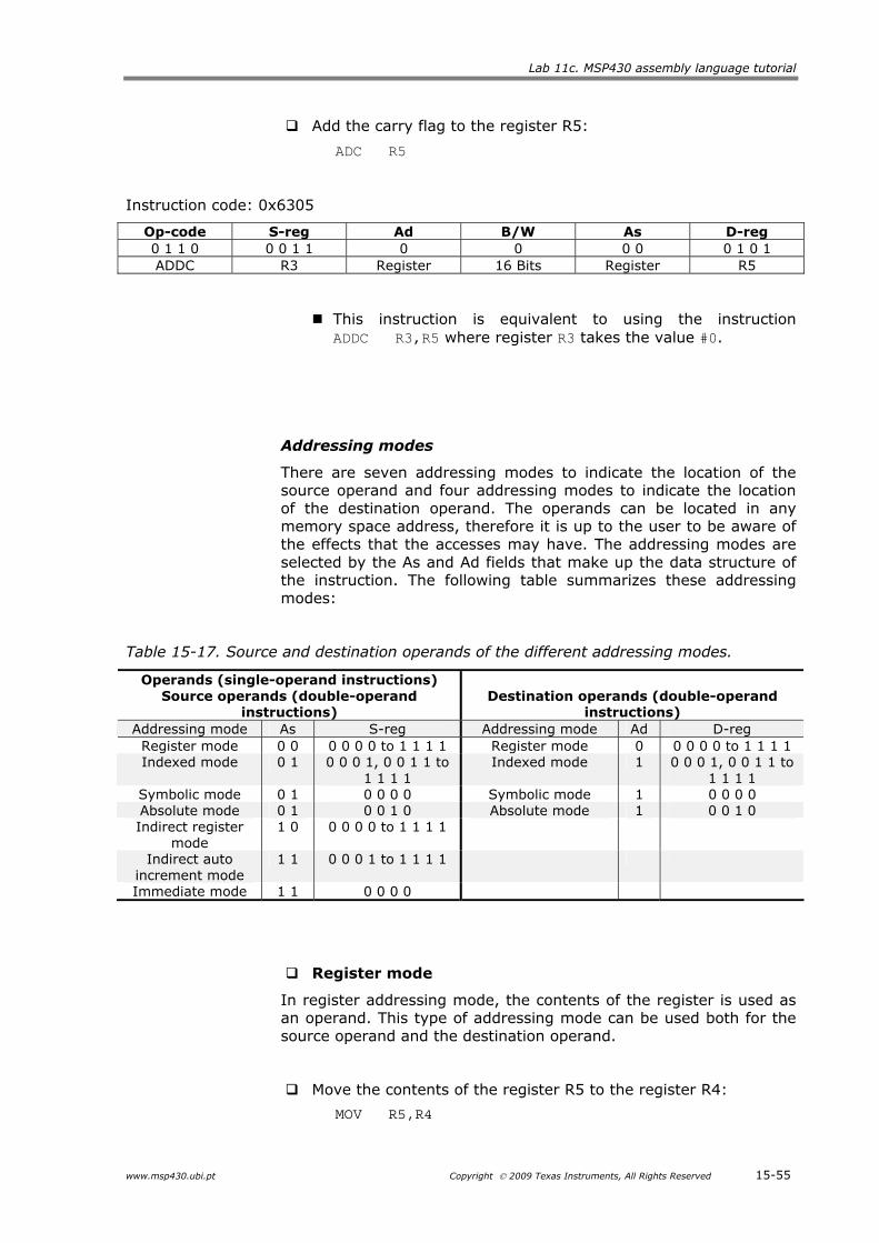
Add the carry flag to the register R5:
ADC R5
Instruction code: 0x6305
Op-code S-reg Ad B/W As D-reg 0 1 1 0 0 0 1 1 0 0 0 0 0 1 0 1 ADDC R3 Register 16 Bits Register R5
This instruction is equivalent to using the instruction ADDC R3,R5 where register R3 takes the value #0.
Addressing modes
There are seven addressing modes to indicate the location of the source operand and four addressing modes to indicate the location of the destination operand. The operands can be located in any memory space address, therefore it is up to the user to be aware of the effects that the accesses may have. The addressing modes are selected by the As and Ad fields that make up the data structure of the instruction. The following table summarizes these addressing modes:
Table 15-17. Source and destination operands of the different addressing modes.
Operands (single-operand instructions) Source operands (double-operand
instructions)
Destination operands (double-operand
instructions) Addressing mode As S-reg Addressing mode Ad D-reg Register mode 0 0 0 0 0 0 to 1 1 1 1 Register mode 0 0 0 0 0 to 1 1 1 1 Indexed mode 0 1 0 0 0 1, 0 0 1 1 to
1 1 1 1 Indexed mode 1 0 0 0 1, 0 0 1 1 to
1 1 1 1 Symbolic mode 0 1 0 0 0 0 Symbolic mode 1 0 0 0 0 Absolute mode 0 1 0 0 1 0 Absolute mode 1 0 0 1 0 Indirect register
mode 1 0 0 0 0 0 to 1 1 1 1
Indirect auto increment mode
1 1 0 0 0 1 to 1 1 1 1
Immediate mode 1 1 0 0 0 0
Register mode
In register addressing mode, the contents of the register is used as an operand. This type of addressing mode can be used both for the source operand and the destination operand.
Move the contents of the register R5 to the register R4:
MOV R5,R4
Advanced Laboratories
15-56 Copyright 2009 Texas Instruments, All Rights Reserved www.msp430.ubi.pt
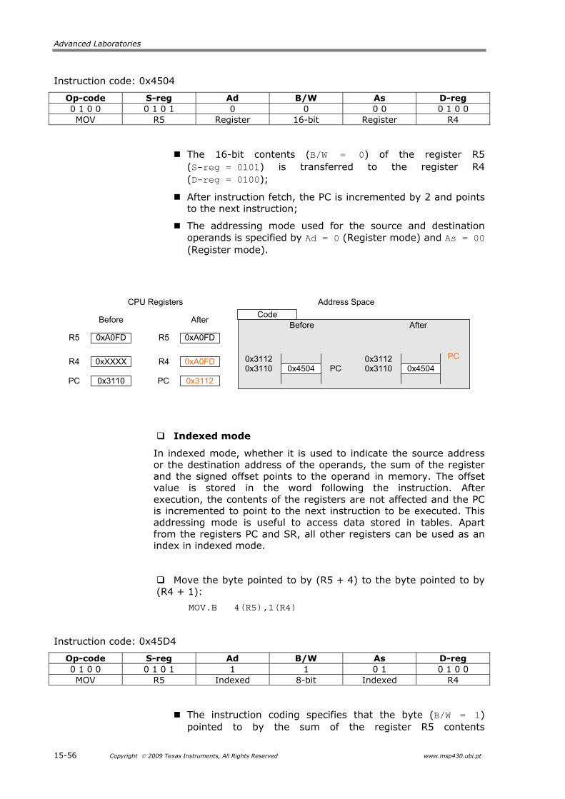
Instruction code: 0x4504
Op-code S-reg Ad B/W As D-reg 0 1 0 0 0 1 0 1 0 0 0 0 0 1 0 0 MOV R5 Register 16-bit Register R4
The 16-bit contents (B/W = 0) of the register R5 (S-reg = 0101) is transferred to the register R4 (D-reg = 0100);
After instruction fetch, the PC is incremented by 2 and points to the next instruction;
The addressing mode used for the source and destination operands is specified by Ad = 0 (Register mode) and As = 00 (Register mode).
CPU Registers
Before After
0x3110PC 0x3112PC
0xXXXXR4 R4 0xA0FD
0xA0FDR5 0xA0FDR5
Address Space
0x4504 PC0x31100x3112
0x4504
PC
0x31100x3112
Before AfterCode
Indexed mode
In indexed mode, whether it is used to indicate the source address or the destination address of the operands, the sum of the register and the signed offset points to the operand in memory. The offset value is stored in the word following the instruction. After execution, the contents of the registers are not affected and the PC is incremented to point to the next instruction to be executed. This addressing mode is useful to access data stored in tables. Apart from the registers PC and SR, all other registers can be used as an index in indexed mode.
Move the byte pointed to by (R5 + 4) to the byte pointed to by (R4 + 1):
MOV.B 4(R5),1(R4)
Instruction code: 0x45D4
Op-code S-reg Ad B/W As D-reg 0 1 0 0 0 1 0 1 1 1 0 1 0 1 0 0 MOV R5 Indexed 8-bit Indexed R4
The instruction coding specifies that the byte (B/W = 1) pointed to by the sum of the register R5 contents
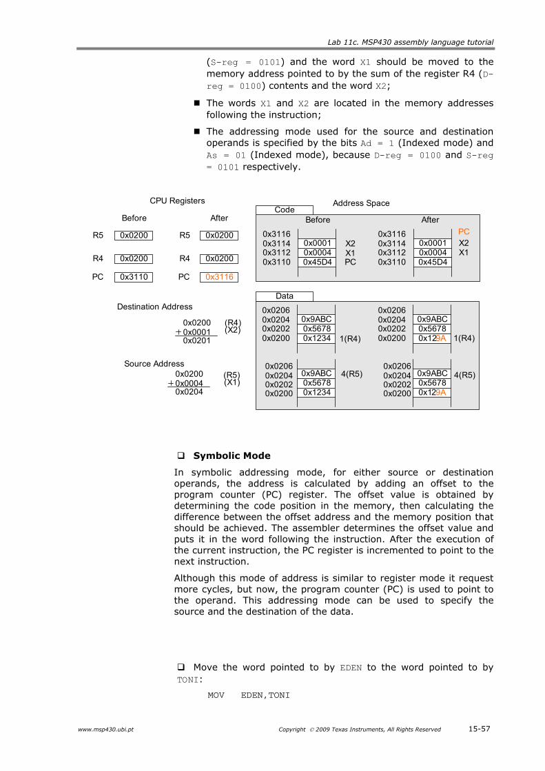
Lab 11c. MSP430 assembly language tutorial
www.msp430.ubi.pt Copyright 2009 Texas Instruments, All Rights Reserved 15-57
(S-reg = 0101) and the word X1 should be moved to the memory address pointed to by the sum of the register R4 (D-reg = 0100) contents and the word X2;
The words X1 and X2 are located in the memory addresses following the instruction;
The addressing mode used for the source and destination operands is specified by the bits Ad = 1 (Indexed mode) and As = 01 (Indexed mode), because D-reg = 0100 and S-reg = 0101 respectively.
Data
CPU Registers
Before After
0x3110PC 0x3116PC
0x0200R4 R4 0x0200
0x0200R5 0x0200R5
Address Space
0x02000x00040x0204
0x9ABC0x56780x1234
0x9ABC0x56780x129A
4(R5)
0x02000x02020x02040x0206
0x02000x02020x02040x0206
4(R5)
0x02000x00010x0201
0x9ABC0x56780x12340x0200
0x02020x02040x0206
0x9ABC0x56780x129A0x0200
0x02020x02040x0206
1(R4) 1(R4)
0x00010x00040x45D4 PC0x3110
0x31120x31140x3116
0x00010x00040x45D4
PC
0x31100x31120x31140x3116
Before AfterCode
X1X2
X1X2
Destination Address
Source Address
(R4)(X2)
(R5)(X1)
Symbolic Mode
In symbolic addressing mode, for either source or destination operands, the address is calculated by adding an offset to the program counter (PC) register. The offset value is obtained by determining the code position in the memory, then calculating the difference between the offset address and the memory position that should be achieved. The assembler determines the offset value and puts it in the word following the instruction. After the execution of the current instruction, the PC register is incremented to point to the next instruction.
Although this mode of address is similar to register mode it request more cycles, but now, the program counter (PC) is used to point to the operand. This addressing mode can be used to specify the source and the destination of the data.
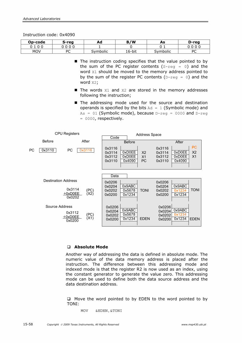
Move the word pointed to by EDEN to the word pointed to by TONI:
MOV EDEN,TONI
Advanced Laboratories
15-58 Copyright 2009 Texas Instruments, All Rights Reserved www.msp430.ubi.pt
Instruction code: 0x4090
Op-code S-reg Ad B/W As D-reg 0 1 0 0 0 0 0 0 1 0 0 1 0 0 0 0 MOV PC Symbolic 16-bit Symbolic PC
The instruction coding specifies that the value pointed to by
the sum of the PC register contents (S-reg = 0) and the word X1 should be moved to the memory address pointed to by the sum of the register PC contents (D-reg = 0) and the word X2;
The words X1 and X2 are stored in the memory addresses following the instruction;
The addressing mode used for the source and destination operands is specified by the bits Ad = 1 (Symbolic mode) and As = 01 (Symbolic mode), because D-reg = 0000 and S-reg = 0000, respectively.
Data
CPU Registers
Before After
Address Space
0x9ABC0x56780x1234
0x9ABC0x12340x1234EDEN0x0200
0x02020x02040x0206
0x02000x02020x02040x0206
EDEN
0x9ABC0x56780x12340x0200
0x02020x02040x0206
0x9ABC0x12340x12340x0200
0x02020x02040x0206
TONI TONI
0xD0EE0xD0EE0x4090 PC0x3110
0x31120x31140x3116
0xD0EE0xD0EE0x4090
PC
0x31100x31120x31140x3116
Before AfterCode
X1X2
X1X2
0x3110PC 0x3116PC
0x31120xD0EE0x0200
0x31140xD0EE0x0202
Destination Address
Source Address
(PC)(X2)
(PC)(X1)
Absolute Mode
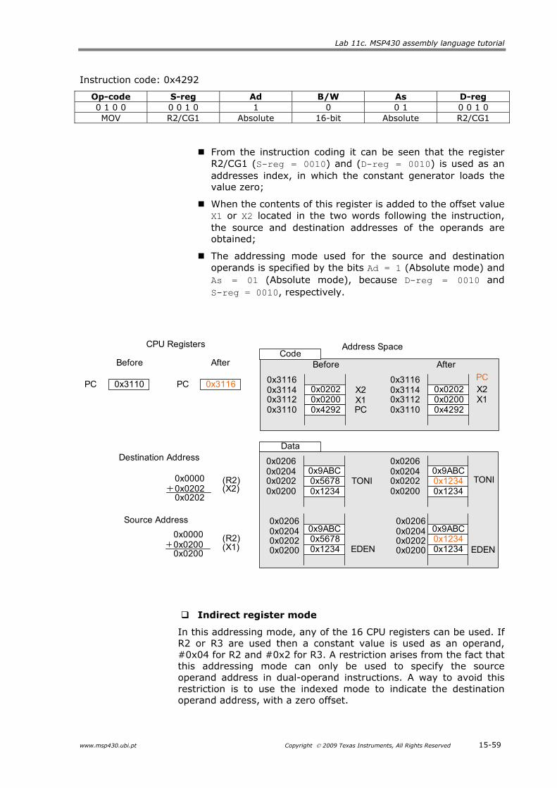
Another way of addressing the data is defined in absolute mode. The numeric value of the data memory address is placed after the instruction. The difference between this addressing mode and indexed mode is that the register R2 is now used as an index, using the constant generator to generate the value zero. This addressing mode can be used to define both the data source address and the data destination address.
Move the word pointed to by EDEN to the word pointed to by TONI:
MOV &EDEN,&TONI
Lab 11c. MSP430 assembly language tutorial
www.msp430.ubi.pt Copyright 2009 Texas Instruments, All Rights Reserved 15-59
Instruction code: 0x4292
Op-code S-reg Ad B/W As D-reg 0 1 0 0 0 0 1 0 1 0 0 1 0 0 1 0 MOV R2/CG1 Absolute 16-bit Absolute R2/CG1
From the instruction coding it can be seen that the register R2/CG1 (S-reg = 0010) and (D-reg = 0010) is used as an addresses index, in which the constant generator loads the value zero;
When the contents of this register is added to the offset value X1 or X2 located in the two words following the instruction, the source and destination addresses of the operands are obtained;
The addressing mode used for the source and destination operands is specified by the bits Ad = 1 (Absolute mode) and As = 01 (Absolute mode), because D-reg = 0010 and S-reg = 0010, respectively.
Data
CPU Registers
Before After
Address Space
0x9ABC0x56780x1234
0x9ABC0x12340x1234EDEN0x0200
0x02020x02040x0206
0x02000x02020x02040x0206
EDEN
0x9ABC0x56780x12340x0200
0x02020x02040x0206
0x9ABC0x12340x12340x0200
0x02020x02040x0206
TONI TONI
0x02020x02000x4292 PC0x3110
0x31120x31140x3116
0x02020x02000x4292
PC
0x31100x31120x31140x3116
Before AfterCode
X1X2
X1X2
0x3110PC 0x3116PC
0x00000x02000x0200
0x00000x02020x0202
Destination Address
Source Address
(R2)(X2)
(R2)(X1)
Indirect register mode
In this addressing mode, any of the 16 CPU registers can be used. If R2 or R3 are used then a constant value is used as an operand, #0x04 for R2 and #0x2 for R3. A restriction arises from the fact that this addressing mode can only be used to specify the source operand address in dual-operand instructions. A way to avoid this restriction is to use the indexed mode to indicate the destination operand address, with a zero offset.

Advanced Laboratories
15-60 Copyright 2009 Texas Instruments, All Rights Reserved www.msp430.ubi.pt
Move the word pointed to by R5 to the word pointed to by R4:
MOV @R5,0(R4)
Instruction code: 0x45A4
Op-code S-reg Ad B/W As D-reg 0 1 0 0 0 1 0 1 1 0 1 0 0 1 0 0 MOV R5 Indexed 16-bit Indirect R4
The instruction coding specifies that the register R5 (S-reg = 0101) has the source address (As = 10);
The destination address is pointed to in indexed mode (Ad = 1) by R4 (D-reg = 0100), using a zero value offset.
Data
CPU Registers
Before After
Address Space
0x9ABC0x56780x1234
0x9ABC0x12340x1234@R50x0200
0x02020x02040x0206
0x02000x02020x02040x0206
@R5
0x9ABC0x56780x12340x0200
0x02020x02040x0206
0x9ABC0x12340x12340x0200
0x02020x02040x0206
0(R4) 0(R4)
0x00000x45A4 PC0x3110
0x31120x3114
0x00000x45A4
PC
0x31100x31120x3114
Before AfterCode
X1 X1
0x3110PC 0x3114PC
0x02020x00000x0202
Destination Address
Source Address
(R4)(X1)
0x0202R4 R4 0x0202
0x0200R5 0x0200R5
Indirect auto-increment mode
This addressing mode is similar to the previous one. The contents of the source register are incremented according to the data type processed. If the data value is of size byte, the source register is incremented by 1. If the data value is of size word, the register is incremented by 2. Note that this addressing mode can only be used to define the source operand in dual-operand instructions.
Move the word pointed to by R5 to the word pointed to by R4, and increment the source pointer:
MOV @R5+,0(R4)

Lab 11c. MSP430 assembly language tutorial
www.msp430.ubi.pt Copyright 2009 Texas Instruments, All Rights Reserved 15-61
Instruction code: 0x45B4
Op-code S-reg Ad B/W As D-reg 0 1 0 0 0 1 0 1 1 0 1 1 0 1 0 0 MOV R5 Indexed 16-bit Ind. aut. inc. R4
The instruction coding specifies that the register R5 (S-reg = 0101) has the source address with As = 11;
The destination address is pointed to in indexed mode by R4 (D-reg = 0100), using a zero value as offset;
The execution of the instruction increments the contents of the register R5 by 2.
Data
CPU Registers
Before After
Address Space
0x9ABC0x56780x1234
0x9ABC0x12340x1234@R50x0200
0x02020x02040x0206
0x02000x02020x02040x0206
@R5
0x9ABC0x56780x12340x0200
0x02020x02040x0206
0x9ABC0x12340x12340x0200
0x02020x02040x0206
0(R4) 0(R4)
0x00000x45A4 PC0x3110
0x31120x3114
0x00000x45A4
PC
0x31100x31120x3114
Before AfterCode
X1 X1
0x3110PC 0x3114PC
0x02020x00000x0202
Destination Address
Source Address
(R4)(X1)
0x0202R4 R4 0x0202
0x0200R5 0x0202R5
Immediate mode
The immediate addressing mode allows loading values in registers or memory addresses. It can only be used as a source operand.
Move the value 0x0200 to R5:
MOV #0x0200,R5
Instruction code: 0x4035
Op-code S-reg Ad B/W As D-reg 0 1 0 0 0 0 0 0 0 0 1 1 0 1 0 1 MOV PC Register 16-bit Immediate R5

Advanced Laboratories
15-62 Copyright 2009 Texas Instruments, All Rights Reserved www.msp430.ubi.pt
The instruction coding specifies that the register PC (S-reg = 0000) is used to define the location of the word in memory that loads the register R5 (D-reg = 0101) with Ad = 11.
CPU Registers
Before After
Address Space
0x02000x4035 PC0x3110
0x31120x3114
0x02000x4035
PC
0x31100x31120x3114
Before AfterCode
X1 X10x3110PC 0x3114PC
0xXXXXR5 0x0200R5
15.3.2 Exploring the addressing modes of the MSP430X CPU architecture
Main features of the MSP430X CPU architecture
The MSP430X CPU extends the addressing capabilities of the MSP430 family beyond 64 kB to 1 MB. To achieve this, there are some changes to the addressing modes and two new types of instructions. One type of new instructions allows access to the entire address space, and the other is designed for address calculations.
The MSP430X CPU address bus is 20 bits, but the data bus is still 16 bits. The CPU supports 8-bit, 16-bit and 20-bit memory accesses. Despite these changes, the MSP430X CPU remains compatible with the MSP430 CPU, having a similar number of registers. A block diagram of the MSP430X CPU is shown in the figure below:

Lab 11c. MSP430 assembly language tutorial
www.msp430.ubi.pt Copyright 2009 Texas Instruments, All Rights Reserved 15-63
Figure 15-45. MSP430X CPU block diagram.
Although the MSP430X CPU structure is similar to that of the MSP430 CPU, there are some differences that will now be discussed.
With the exception of the status register SR, all MSP430X registers are 20 bits. The CPU can now process 20-bit or 16-bit data.
R0 (PC) - Program Counter
Has the same function as the MSP430 CPU, although now it has 20 bits.

Advanced Laboratories
15-64 Copyright 2009 Texas Instruments, All Rights Reserved www.msp430.ubi.pt
R1 (SP) - Stack Pointer
Has the same function as the MSP430 CPU, although now it has 20 bits.
R2 (SR) - Status Register
Has the same function as the MSP430 CPU, but still only has 16 bits.
Table 15-18. Description of the SR bits.
R2 (CG1) and R3 (CG2) - Constant Generators
The registers R2 and R3 can be used to generate six different constants commonly used in programming, without the need to add an extra 16-bit word of code to the instruction. The constants below are chosen based on the bit (As) of the instruction that selects the addressing mode.
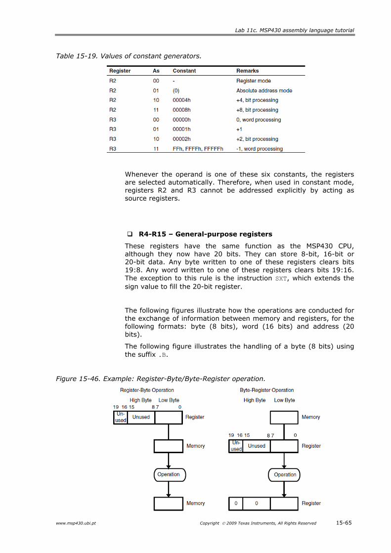
Lab 11c. MSP430 assembly language tutorial
www.msp430.ubi.pt Copyright 2009 Texas Instruments, All Rights Reserved 15-65
Table 15-19. Values of constant generators.
Whenever the operand is one of these six constants, the registers are selected automatically. Therefore, when used in constant mode, registers R2 and R3 cannot be addressed explicitly by acting as source registers.
R4-R15 – General-purpose registers
These registers have the same function as the MSP430 CPU, although they now have 20 bits. They can store 8-bit, 16-bit or 20-bit data. Any byte written to one of these registers clears bits 19:8. Any word written to one of these registers clears bits 19:16. The exception to this rule is the instruction SXT, which extends the sign value to fill the 20-bit register.
The following figures illustrate how the operations are conducted for the exchange of information between memory and registers, for the following formats: byte (8 bits), word (16 bits) and address (20 bits).
The following figure illustrates the handling of a byte (8 bits) using the suffix .B.
Figure 15-46. Example: Register-Byte/Byte-Register operation.

Advanced Laboratories
15-66 Copyright 2009 Texas Instruments, All Rights Reserved www.msp430.ubi.pt
The following figure illustrates the handling of a word (16-bit) using the suffix .W.
Figure 15-47. Example: Register-Word/Word-Register operation.
The following figure illustrates the manipulation of an address (20 bits) using the suffix .A.
Figure 15-48. Example: Register - Address-Word operation.
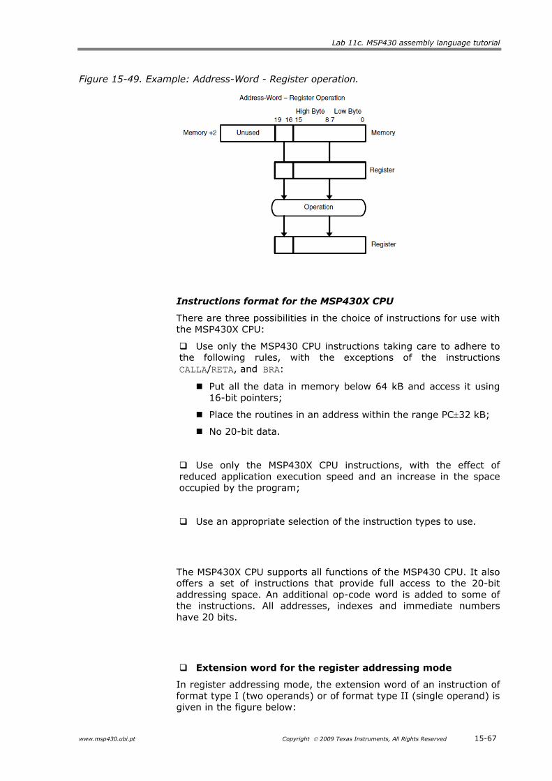
Lab 11c. MSP430 assembly language tutorial
www.msp430.ubi.pt Copyright 2009 Texas Instruments, All Rights Reserved 15-67
Figure 15-49. Example: Address-Word - Register operation.
Instructions format for the MSP430X CPU
There are three possibilities in the choice of instructions for use with the MSP430X CPU:
Use only the MSP430 CPU instructions taking care to adhere to the following rules, with the exceptions of the instructions CALLA/RETA, and BRA:
Put all the data in memory below 64 kB and access it using 16-bit pointers;
Place the routines in an address within the range PC32 kB;
No 20-bit data.
Use only the MSP430X CPU instructions, with the effect of reduced application execution speed and an increase in the space occupied by the program;
Use an appropriate selection of the instruction types to use.
The MSP430X CPU supports all functions of the MSP430 CPU. It also offers a set of instructions that provide full access to the 20-bit addressing space. An additional op-code word is added to some of the instructions. All addresses, indexes and immediate numbers have 20 bits.
Extension word for the register addressing mode
In register addressing mode, the extension word of an instruction of format type I (two operands) or of format type II (single operand) is given in the figure below:
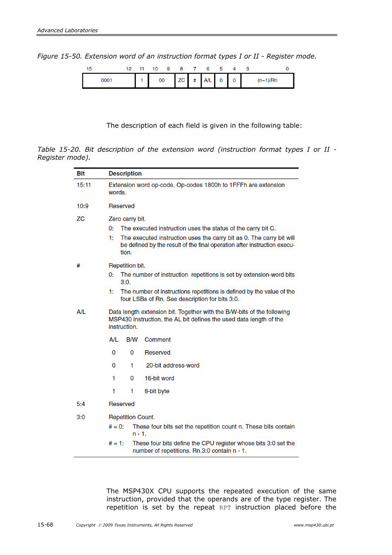
Advanced Laboratories
15-68 Copyright 2009 Texas Instruments, All Rights Reserved www.msp430.ubi.pt
Figure 15-50. Extension word of an instruction format types I or II - Register mode.
The description of each field is given in the following table:
Table 15-20. Bit description of the extension word (instruction format types I or II - Register mode).
The MSP430X CPU supports the repeated execution of the same instruction, provided that the operands are of the type register. The repetition is set by the repeat RPT instruction placed before the
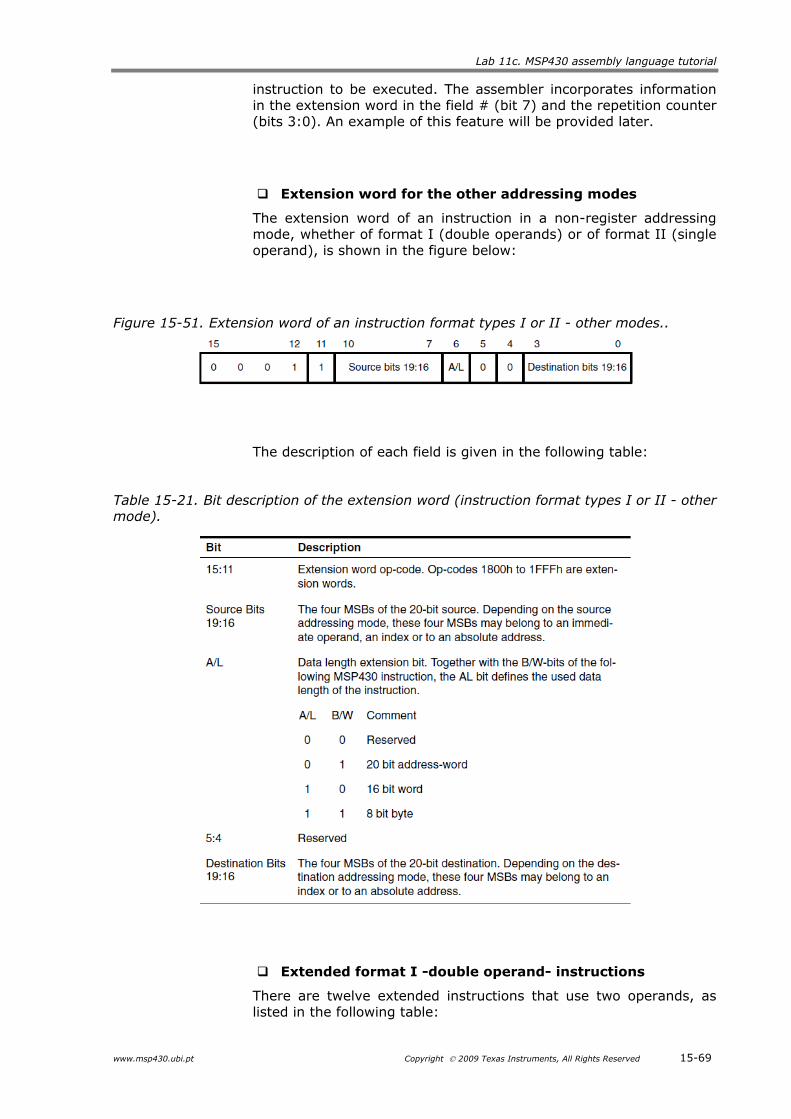
Lab 11c. MSP430 assembly language tutorial
www.msp430.ubi.pt Copyright 2009 Texas Instruments, All Rights Reserved 15-69
instruction to be executed. The assembler incorporates information in the extension word in the field # (bit 7) and the repetition counter (bits 3:0). An example of this feature will be provided later.
Extension word for the other addressing modes
The extension word of an instruction in a non-register addressing mode, whether of format I (double operands) or of format II (single operand), is shown in the figure below:
Figure 15-51. Extension word of an instruction format types I or II - other modes..
The description of each field is given in the following table:
Table 15-21. Bit description of the extension word (instruction format types I or II - other mode).
Extended format I -double operand- instructions
There are twelve extended instructions that use two operands, as listed in the following table:
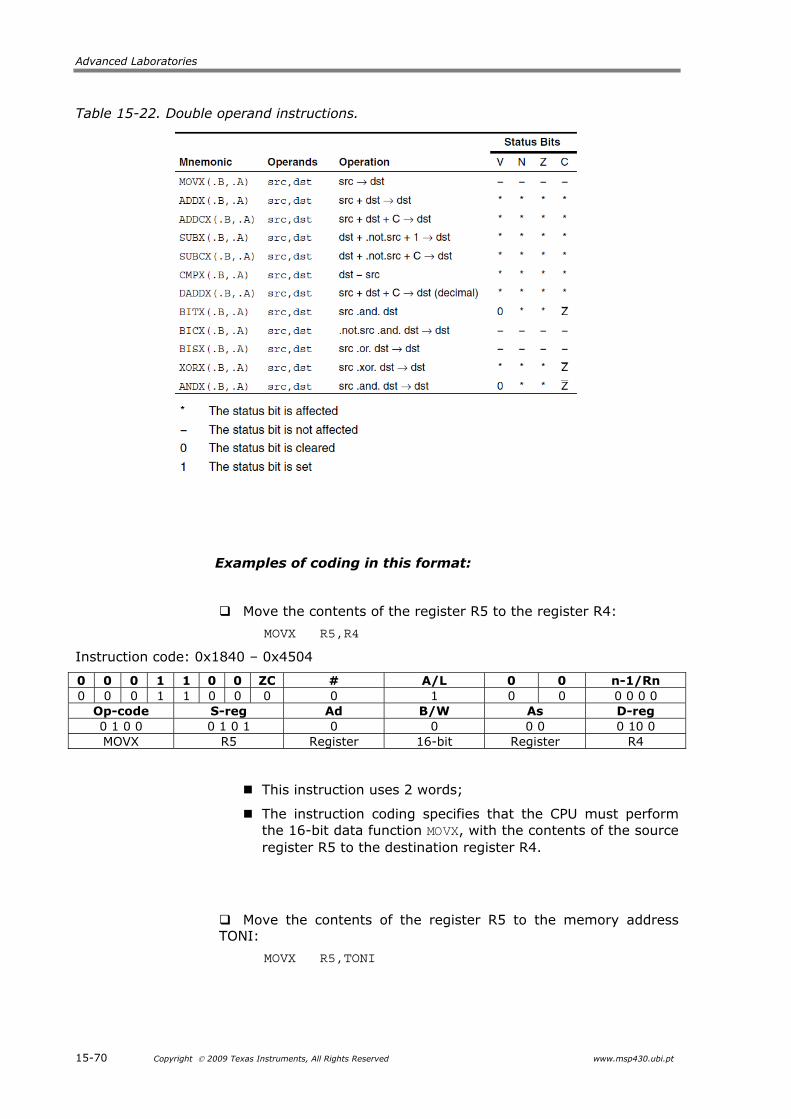
Advanced Laboratories
15-70 Copyright 2009 Texas Instruments, All Rights Reserved www.msp430.ubi.pt
Table 15-22. Double operand instructions.
Examples of coding in this format:
Move the contents of the register R5 to the register R4:
MOVX R5,R4
Instruction code: 0x1840 – 0x4504
0 0 0 1 1 0 0 ZC # A/L 0 0 n-1/Rn 0 0 0 1 1 0 0 0 0 1 0 0 0 0 0 0
Op-code S-reg Ad B/W As D-reg 0 1 0 0 0 1 0 1 0 0 0 0 0 10 0 MOVX R5 Register 16-bit Register R4
This instruction uses 2 words;
The instruction coding specifies that the CPU must perform the 16-bit data function MOVX, with the contents of the source register R5 to the destination register R4.
Move the contents of the register R5 to the memory address TONI:
MOVX R5,TONI

Lab 11c. MSP430 assembly language tutorial
www.msp430.ubi.pt Copyright 2009 Texas Instruments, All Rights Reserved 15-71
Instruction code: 0x184F – 0x4580
0 0 0 1 1 src 19:16 A/L 0 0 dst 19:16 0 0 0 1 1 0 0 0 0 1 0 0 1 1 1 1
Op-code S-reg Ad B/W As D-reg 0 1 0 0 0 1 0 1 1 0 0 0 0 0 0 0 MOVX R5 Symbolic 16-bits Register PC
This instruction uses 3 words;
The instruction coding specifies that the CPU must perform the 16-bit data function MOVX, the source being the contents of register R5 and the destination being the memory address pointed to by (dst 19:16: X1 + PC);
The destination (dst bits 19:16) is stored in the extension word and the word X1 is stored in the word following the instruction.
Move the contents of the memory address TONI to the register R5:
MOVX TONI,R5
Instruction code: 0x1FC0 – 0x4015
0 0 0 1 1 src 19:16 A/L 0 0 dst 19:16 0 0 0 1 1 1 1 1 1 1 0 0 0 0 0 0
Op-code S-reg Ad B/W As D-reg 0 1 0 0 0 0 0 0 0 0 0 1 0 1 0 1 MOVX PC Register 16-bit Symbolic R5
This instruction uses 3 words;
The instruction coding specifies that the CPU must perform the 16-bit data function MOVX, the source being the contents of memory address pointed to by (src 19:16: X1 + PC) and the destination being register R5;
The destination (dst bits 19:16) are stored in the extension word and the word X1 is stored in the word following the instruction.
Move the contents of the memory address TONI to the address memory EDEN:
MOVX TONI,EDEN
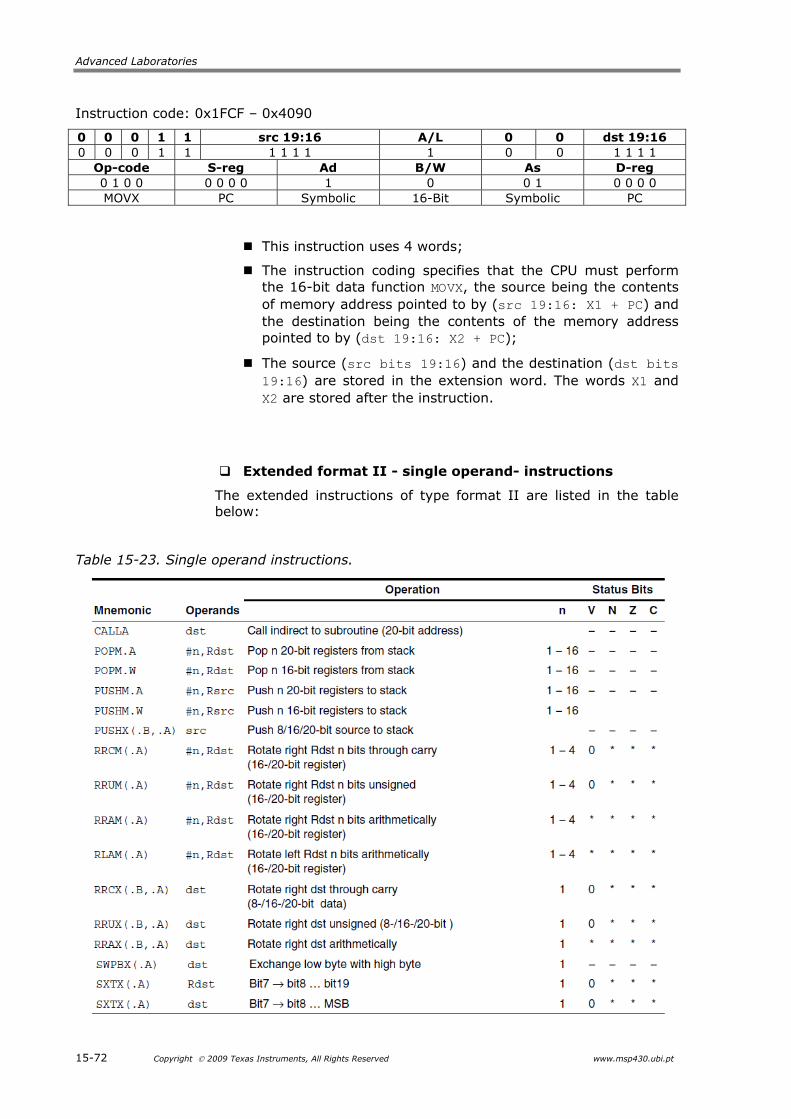
Advanced Laboratories
15-72 Copyright 2009 Texas Instruments, All Rights Reserved www.msp430.ubi.pt
Instruction code: 0x1FCF – 0x4090
0 0 0 1 1 src 19:16 A/L 0 0 dst 19:16 0 0 0 1 1 1 1 1 1 1 0 0 1 1 1 1
Op-code S-reg Ad B/W As D-reg 0 1 0 0 0 0 0 0 1 0 0 1 0 0 0 0 MOVX PC Symbolic 16-Bit Symbolic PC
This instruction uses 4 words;
The instruction coding specifies that the CPU must perform the 16-bit data function MOVX, the source being the contents of memory address pointed to by (src 19:16: X1 + PC) and the destination being the contents of the memory address pointed to by (dst 19:16: X2 + PC);
The source (src bits 19:16) and the destination (dst bits 19:16) are stored in the extension word. The words X1 and X2 are stored after the instruction.
Extended format II - single operand- instructions
The extended instructions of type format II are listed in the table below:
Table 15-23. Single operand instructions.

Lab 11c. MSP430 assembly language tutorial
www.msp430.ubi.pt Copyright 2009 Texas Instruments, All Rights Reserved 15-73
The MSP430X CPU has some capabilities in additional to those of the MSP430 CPU:
The ability to place and remove several registers to/from the stack using only a single instruction;
The ability to perform several rotations on the contents of a register.
Examples of coding in this format:
Rotate right the 20-bit contents of the register R5 with the carry flag:
RRCX.A R5
Instruction code: 0x1800 – 0x1045
0 0 0 1 1 0 0 ZC # A/L 0 0 n-1/Rn 0 0 0 1 1 0 0 0 0 0 0 0 0 0 0 0
Op-code B/W Ad D/S-reg 0 0 0 1 0 0 0 0 0 1 0 0 0 1 0 1
RRCX 20-bit Register R5
This instruction uses 2 words;
The instruction coding specifies that the CPU must perform the function RRCX using 20-bit data as the contents of register R5.
Rotate right the 20-bit contents of the memory address TONI with carry flag:
RRCX.A TONI
Instruction code: 0x180F – 0x1050
0 0 0 1 1 Src 19:16 A/L 0 0 dst 19:16 0 0 0 1 1 0 0 0 0 0 0 0 1 1 1 1
Op-code B/W Ad D/S-reg 0 0 0 1 0 0 0 0 0 1 0 1 0 0 0 0
RRCX 20-bit Symbolic PC
This instruction uses 3 words;
The instruction coding specifies that the CPU must perform the function RRCX using 20-bit data as the contents of the memory address pointed to by (dst 19:16: X1 + PC);
The destination bits (dst 19:16) are stored in the extension word and the word X1 is stored in the word following the instruction;

Advanced Laboratories
15-74 Copyright 2009 Texas Instruments, All Rights Reserved www.msp430.ubi.pt
As the instruction operand is located in memory, not in a CPU register, two words are used to store the operand, in the format given in the figure below:
Figure 15-52. Single operand format.
There are some exceptions to the representation of the extended format II instructions of the MSP430X CPU. The following examples illustrate these exceptions:
Store the 20-bit registers R10, R9, R8 on the stack:
PUSHM.A #3,R10
The instructions PUSHM and POPM are coded according to the figure given below:
Figure 15-53. PUSHM and POPM coding format.
Instruction code: 0x142A
Op-code n - 1 D-reg 0 0 0 1 0 1 0 0 0 0 1 0 1 0 1 0
PUSHM.A #3 R10
This instruction uses 1 word;
The instruction coding specifies that the CPU must perform the function PUSHM of the 20-bit registers starting at register R10 and ending at register R8;
For three registers 6 words (12 Bytes) of stack are used.

Lab 11c. MSP430 assembly language tutorial
www.msp430.ubi.pt Copyright 2009 Texas Instruments, All Rights Reserved 15-75
Rotate right three times the contents of the 20-bit register R5 with the carry flag:
RRCM.A #3,R5
The instructions RRCM, RRAM, RRUM and RLAM are coded according to the figure below:
Figure 15-54. RRCM, RRAM, RLAM coding format.
Instruction code: 0x0845
C n-1 Op-code R-reg 0 0 0 0 1 0 0 0 0 1 0 0 0 1 0 1
#3 RRCM R5
This instruction uses 1 word;
The instruction coding specifies that the CPU must perform the function RRCM using the 20-bit register R5, a total of 3 times.
Perform a branch in the program flow:
BRA R5
This type of instruction can be coded in three different formats, as show in the figure below:
Figure 15-55. BRA coding format.
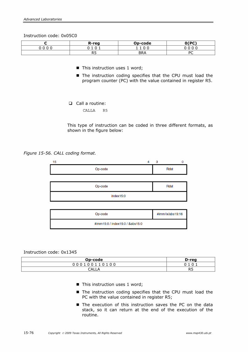
Advanced Laboratories
15-76 Copyright 2009 Texas Instruments, All Rights Reserved www.msp430.ubi.pt
Instruction code: 0x05C0
C R-reg Op-code 0(PC) 0 0 0 0 0 1 0 1 1 1 0 0 0 0 0 0
R5 BRA PC
This instruction uses 1 word;
The instruction coding specifies that the CPU must load the program counter (PC) with the value contained in register R5.
Call a routine:
CALLA R5
This type of instruction can be coded in three different formats, as shown in the figure below:
Figure 15-56. CALL coding format.
Instruction code: 0x1345
Op-code D-reg 0 0 0 1 0 0 1 1 0 1 0 0 0 1 0 1
CALLA R5
This instruction uses 1 word;
The instruction coding specifies that the CPU must load the PC with the value contained in register R5;
The execution of this instruction saves the PC on the data stack, so it can return at the end of the execution of the routine.

Lab 11c. MSP430 assembly language tutorial
www.msp430.ubi.pt Copyright 2009 Texas Instruments, All Rights Reserved 15-77
Extended emulated instructions
The constant generators offer a set of extended emulated instructions, which are listed in the following table:
Table 15-24. Extended emulated instructions.
MSP430X address instructions
The address instructions support 20-bit operands, but they have restrictions on the addressing modes that can be used. A list of extended address instructions, with their supported addressing modes, is given in the following table:
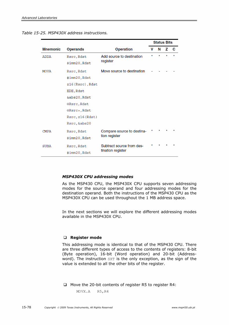
Advanced Laboratories
15-78 Copyright 2009 Texas Instruments, All Rights Reserved www.msp430.ubi.pt
Table 15-25. MSP430X address instructions.
MSP430X CPU addressing modes
As the MSP430 CPU, the MSP430X CPU supports seven addressing modes for the source operand and four addressing modes for the destination operand. Both the instructions of the MSP430 CPU as the MSP430X CPU can be used throughout the 1 MB address space.
In the next sections we will explore the different addressing modes available in the MSP430X CPU.
Register mode
This addressing mode is identical to that of the MSP430 CPU. There are three different types of access to the contents of registers: 8-bit (Byte operation), 16-bit (Word operation) and 20-bit (Address-word). The instruction SXT is the only exception, as the sign of the value is extended to all the other bits of the register.
Move the 20-bit contents of register R5 to register R4:
MOVX.A R5,R4

Lab 11c. MSP430 assembly language tutorial
www.msp430.ubi.pt Copyright 2009 Texas Instruments, All Rights Reserved 15-79
Instruction code: 0x1800 – 0x4544
0 0 0 1 1 0 0 ZC # A/L 0 0 n-1/Rn 0 0 0 1 1 0 0 0 0 0 0 0 0 0 0 0
Op-code S-reg Ad B/W As D-reg 0 1 0 0 0 1 0 1 0 1 0 0 0 1 0 0 MOVX R5 Register 20-bit Register R4
This instruction uses 2 words.
The 20-bit contents (B/W = 1 and A/L = 0) of register R5 (S-reg = 0101) is transferred to register R4 (D-reg = 0100);
After the execution of the instruction, the PC is incremented by 4 and points to the next instruction;
The addressing mode used for the source and destination operands is specified by Ad = 0 (Register mode) and As = 00 (Register mode).
CPU Registers
Before After
0x03110PC 0x03114PC
0xXXXXXR4 R4 0x12345
0x12345R5 0x12345R5
Address Space
0x45440x1800 PC0x03110
0x031120x03114
0x45440x4504
PC
0x031100x031120x03114
Before AfterCode
Indexed mode
The indexed mode can be used in three different situations:
Indexed mode in the memory address space below 64 kB:
If the CPU register Rn points to a memory address located below 64 kB, the address resulting from the sum of the index and the register Rn has the value zero in bits 19:16, thus ensuring that the address is always located in memory below 64 kB.
Move the word pointed to by (R5 - 0x30) to the word pointed to by (R4 + 2):
MOV 0XFFD0(R5),2(R4)

Advanced Laboratories
15-80 Copyright 2009 Texas Instruments, All Rights Reserved www.msp430.ubi.pt
Instruction code: 0x4594
Op-code S-reg Ad B/W As D-reg 0 1 0 0 0 1 0 1 1 0 0 1 0 1 0 0 MOV R5 Indexed 16-bit Indexed R4
This instruction uses 3 words;
The instruction coding specifies that the word (B/W = 0) pointed to by the sum of register R5 contents (S-reg = 0101) with the word X1 should be moved to the memory address pointed to by the sum of register R4 contents (D-reg = 0100) and the word X2;
The words X1 and X2 are located in memory addresses following the instruction;
The addressing mode used for the source and destination operands is specified by the bits Ad = 1 (Indexed mode) and As = 01 (Indexed mode), because D-reg = 0100 and S-reg = 0101 respectively;
In this example, the bits 19:16 are set to zero when the operand addresses have been calculated.
Data
CPU Registers
Before After
0x03110PC 0x03116PC
0x00200R4 R4 0x00200
0x00200R5 0x00200R5
Address Space
0x002000xFFFD00x001D0
0x1234 0x1234X1(R5)0x001D0 0x001D0 X1(R5)
0x002000x000020x00202 0xXXXX0x00202 0x12340x00202X2(R4) X2(R4)
0x00020xFFD00x4594 PC0x03110
0x031120x031140x03116
0x00020xFFD00x4594
PC
Before AfterCode
X1X2
X1X2
Destination Address
Source Address
(R4)(X2)
(R5)(X1)
0x031100x031120x031140x03116
Indexed mode in the memory address space above 64 kB
If the CPU register Rn points to a memory address above 64 kB, bits 19:16 are used to calculate the operand address. A prerequisite is that the operand must be located in the range Rn 32 kB, because the index is a signed 16-bit value. In this case, the operand address can overflow or underflow in memory address space below 64 kB.

Lab 11c. MSP430 assembly language tutorial
www.msp430.ubi.pt Copyright 2009 Texas Instruments, All Rights Reserved 15-81
If a register now points to a memory address space above the 64 kB, the bits 19:16 are used to determine the operand address.
Data
CPU Registers
Before After
0x03110PC 0x03116PC
0x00200R4 R4 0x00200
0x101D0R5 0x101D0R5
Address Space
0x101D00xFFFD00x101A0
0x1234 0x1234X1(R5)0x101A0 0x101A0 X1(R5)
0x002000x000020x00202 0xXXXX0x00202 0x12340x00202X2(R4) X2(R4)
0x00020xFFD00x4594 PC0x03110
0x031120x031140x03116
0x00020xFFD00x4594
PC
Before AfterCode
X1X2
X1X2
Destination Address
Source Address
(R4)(X2)
(R5)(X1)
0x031100x031120x031140x03116
Indexed mode using a MSP430X CPU instruction
When a MSP430X CPU instruction is used in indexed mode, the operand can reside anywhere in the address range Rn 19 bits. The operand address is determined from the sum of the 20-bit contents of the register Rn and the 20-bit signed index.
Move the word pointed to by (R5 – 0x30) to the word pointed to by (R4 + 2):
MOVX 0xFFD0(R5),2(R4)
Instruction code: 0x1FC0 – 0x4594
0 0 0 1 1 src 19:16 A/L 0 0 dst 19:16 0 0 0 1 1 1 1 1 1 1 0 0 0 0 0 0
Op-code S-reg Ad B/W As D-reg 1 0 0 0 0 1 0 1 1 0 0 1 0 1 0 0 MOVX R5 Indexed 16-bit Indexed R4
This instruction uses 4 words;
The instruction coding specifies that the word (B/W = 0 and A/L = 1) pointed to by the sum of register R5 contents (S-reg = 0101) and the word X1 should be moved to the memory address pointed to by the sum the register R4 contents (D-reg = 0100) and the word X2;
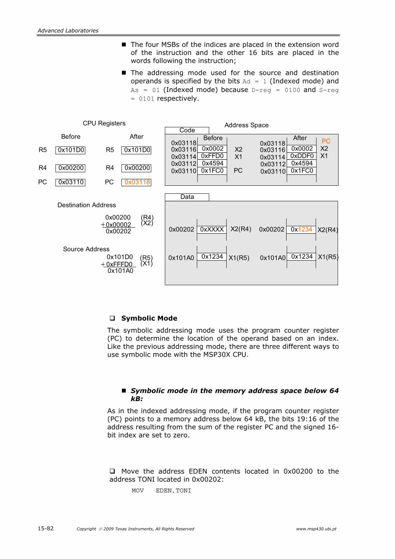
Advanced Laboratories
15-82 Copyright 2009 Texas Instruments, All Rights Reserved www.msp430.ubi.pt
The four MSBs of the indices are placed in the extension word of the instruction and the other 16 bits are placed in the words following the instruction;
The addressing mode used for the source and destination operands is specified by the bits Ad = 1 (Indexed mode) and As = 01 (Indexed mode) because D-reg = 0100 and S-reg = 0101 respectively.
Data
CPU Registers
Before After
0x03110PC 0x03118PC
0x00200R4 R4 0x00200
0x101D0R5 0x101D0R5
Address Space
0x101D00xFFFD00x101A0
0x1234 0x1234X1(R5)0x101A0 0x101A0 X1(R5)
0x002000x000020x00202 0xXXXX0x00202 0x12340x00202X2(R4) X2(R4)
0xFFD00x45940x1FC0 PC
0xDDF00x45940x1FC0
PCBefore AfterCode
X1X2
X1X2
Destination Address
Source Address
(R4)(X2)
(R5)(X1)
0x0002 0x0002
0x031100x031120x031140x031160x03118
0x031100x031120x031140x031160x03118
Symbolic Mode
The symbolic addressing mode uses the program counter register (PC) to determine the location of the operand based on an index. Like the previous addressing mode, there are three different ways to use symbolic mode with the MSP30X CPU.
Symbolic mode in the memory address space below 64 kB:
As in the indexed addressing mode, if the program counter register (PC) points to a memory address below 64 kB, the bits 19:16 of the address resulting from the sum of the register PC and the signed 16-bit index are set to zero.
Move the address EDEN contents located in 0x00200 to the address TONI located in 0x00202:
MOV EDEN,TONI
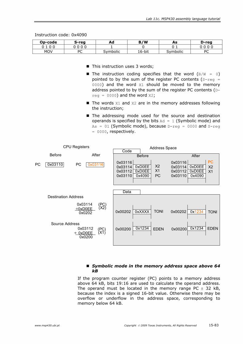
Lab 11c. MSP430 assembly language tutorial
www.msp430.ubi.pt Copyright 2009 Texas Instruments, All Rights Reserved 15-83
Instruction code: 0x4090
Op-code S-reg Ad B/W As D-reg 0 1 0 0 0 0 0 0 1 0 0 1 0 0 0 0 MOV PC Symbolic 16-bit Symbolic PC
This instruction uses 3 words;
The instruction coding specifies that the word (B/W = 0) pointed to by the sum of the register PC contents (S-reg = 0000) and the word X1 should be moved to the memory address pointed to by the sum of the register PC contents (D-reg = 0000) and the word X2;
The words X1 and X2 are in the memory addresses following the instruction;
The addressing mode used for the source and destination operands is specified by the bits Ad = 1 (Symbolic mode) and As = 01 (Symbolic mode), because D-reg = 0000 and S-reg = 0000, respectively.
PC
Data
CPU Registers
Before After
0x03110 0x03116PC
Address Space
0x031120xD0EE0x0200
0x1234 0x1234EDEN0x00200 0x00200 EDEN
0x031140xD0EE0x0202 0xXXXX0x00202 0x12340x00202TONI TONI
0xD0EE0xD0EE0x4090 PC0x03110
0x031120x031140x03116
0xD0EE0xD0EE0x4090
PC
0x031100x031120x031140x03116
Before AfterCode
X1X2
X1X2
Destination Address
Source Address
(PC)(X2)
(PC)(X1)
Symbolic mode in the memory address space above 64 kB
If the program counter register (PC) points to a memory address above 64 kB, bits 19:16 are used to calculate the operand address. The operand must be located in the memory range PC 32 kB, because the index is a signed 16-bit value. Otherwise there may be overflow or underflow in the address space, corresponding to memory below 64 kB.
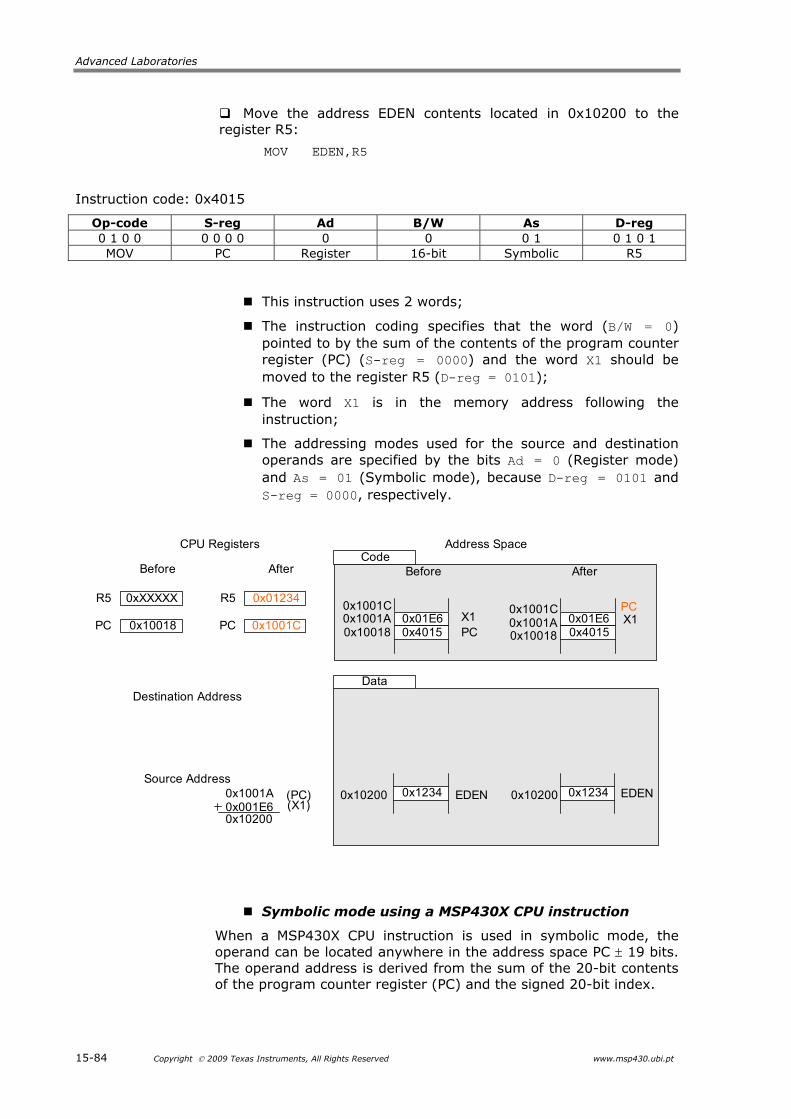
Advanced Laboratories
15-84 Copyright 2009 Texas Instruments, All Rights Reserved www.msp430.ubi.pt
Move the address EDEN contents located in 0x10200 to the register R5:
MOV EDEN,R5
Instruction code: 0x4015
Op-code S-reg Ad B/W As D-reg 0 1 0 0 0 0 0 0 0 0 0 1 0 1 0 1 MOV PC Register 16-bit Symbolic R5
This instruction uses 2 words;
The instruction coding specifies that the word (B/W = 0) pointed to by the sum of the contents of the program counter register (PC) (S-reg = 0000) and the word X1 should be moved to the register R5 (D-reg = 0101);
The word X1 is in the memory address following the instruction;
The addressing modes used for the source and destination operands are specified by the bits Ad = 0 (Register mode) and As = 01 (Symbolic mode), because D-reg = 0101 and S-reg = 0000, respectively.
R5
Data
CPU Registers
Before After
0xXXXXX 0x01234R5
Address Space
0x1001A0x001E60x10200
0x1234 0x1234EDEN0x10200 0x10200 EDEN
0x01E60x4015 PC0x10018
0x1001A0x1001C
0x01E60x4015
PC
Before AfterCode
X1 X1
Destination Address
Source Address(PC)(X1)
0x100180x1001A0x1001C
PC 0x10018 0x1001CPC
Symbolic mode using a MSP430X CPU instruction
When a MSP430X CPU instruction is used in symbolic mode, the operand can be located anywhere in the address space PC 19 bits. The operand address is derived from the sum of the 20-bit contents of the program counter register (PC) and the signed 20-bit index.

Lab 11c. MSP430 assembly language tutorial
www.msp430.ubi.pt Copyright 2009 Texas Instruments, All Rights Reserved 15-85
Move the address EDEN contents located in 0x00200 to the register R5:
MOVX EDEN,R5
Instruction code: 0x1FC0 – 0x4015
0 0 0 1 1 src 19:16 A/L 0 0 dst 19:16 0 0 0 1 1 1 1 1 1 1 0 0 0 0 0 0
Op-code S-reg Ad B/W As D-reg 0 1 0 0 0 0 0 0 0 0 0 1 0 1 0 1 MOVX PC Register 16-bit Symbolic R5
This instruction uses 3 words;
The instruction coding specifies that the CPU must perform the function MOVX of 16-bit data (B/W = 0 and A/L = 1), from the contents of the memory address pointed to by (src 19:16:X1 + PC) to the register R5;
The bits src 19:16 are stored in the extension word and the word X1 is stored after the instruction;
The addressing modes used for the source and destination operands are specified by the bits Ad = 0 (Register mode) and As = 01 (Symbolic mode), because D-reg = 0000 and S-reg = 0101, respectively.
R5
Data
CPU Registers
Before After
0xXXXXX 0x01234R5
Address Space
0x031140xFD0EC0x00200
0x1234 0x1234EDEN0x00200 0x00200 EDEN
0xD0EC0x40150x1FC0 PC0x03110
0x031120x031140x03116
0xD0EC0x40150x1FC0
PC
0x031100x031120x031140x03116
Before AfterCode
X1 X1
Destination Address
Source Address(PC)(X1)
PC 0x03110 0x03116PC
Absolute Mode
Absolute mode uses the word contents following the instruction as the operand address. There are two different ways to use absolute mode with the MSP30X CPU.
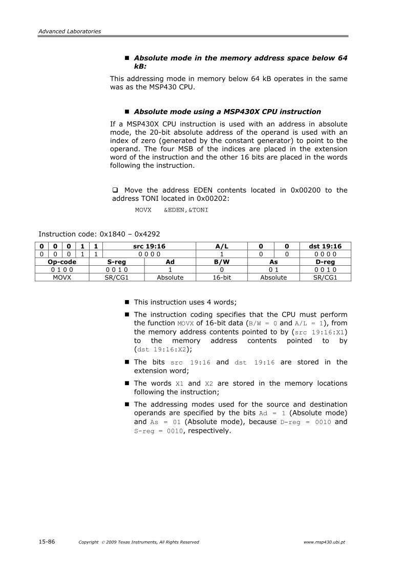
Advanced Laboratories
15-86 Copyright 2009 Texas Instruments, All Rights Reserved www.msp430.ubi.pt
Absolute mode in the memory address space below 64 kB:
This addressing mode in memory below 64 kB operates in the same was as the MSP430 CPU.
Absolute mode using a MSP430X CPU instruction
If a MSP430X CPU instruction is used with an address in absolute mode, the 20-bit absolute address of the operand is used with an index of zero (generated by the constant generator) to point to the operand. The four MSB of the indices are placed in the extension word of the instruction and the other 16 bits are placed in the words following the instruction.
Move the address EDEN contents located in 0x00200 to the address TONI located in 0x00202:
MOVX &EDEN,&TONI
Instruction code: 0x1840 – 0x4292
0 0 0 1 1 src 19:16 A/L 0 0 dst 19:16 0 0 0 1 1 0 0 0 0 1 0 0 0 0 0 0
Op-code S-reg Ad B/W As D-reg 0 1 0 0 0 0 1 0 1 0 0 1 0 0 1 0 MOVX SR/CG1 Absolute 16-bit Absolute SR/CG1
This instruction uses 4 words;
The instruction coding specifies that the CPU must perform the function MOVX of 16-bit data (B/W = 0 and A/L = 1), from the memory address contents pointed to by (src 19:16:X1) to the memory address contents pointed to by (dst 19:16:X2);
The bits src 19:16 and dst 19:16 are stored in the extension word;
The words X1 and X2 are stored in the memory locations following the instruction;
The addressing modes used for the source and destination operands are specified by the bits Ad = 1 (Absolute mode) and As = 01 (Absolute mode), because D-reg = 0010 and S-reg = 0010, respectively.
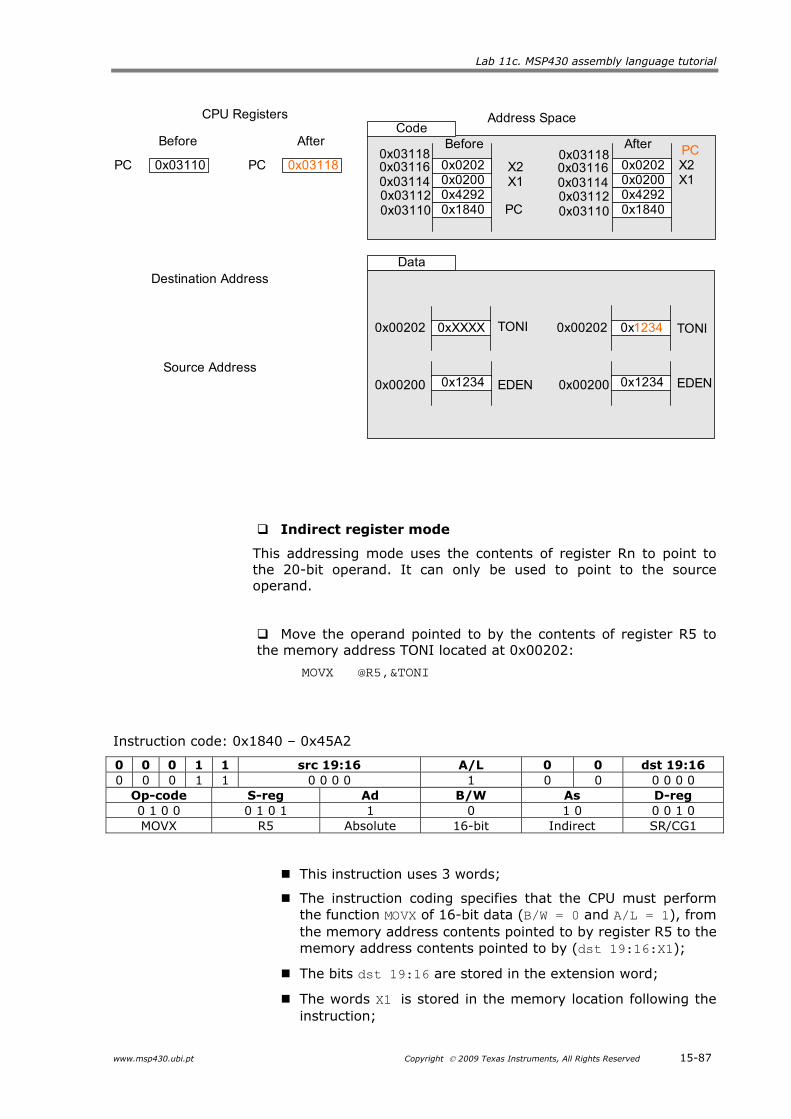
Lab 11c. MSP430 assembly language tutorial
www.msp430.ubi.pt Copyright 2009 Texas Instruments, All Rights Reserved 15-87
Data
CPU Registers
Before After
0x03110PC 0x03118PC
Address Space
0x1234 0x1234EDEN0x00200 0x00200 EDEN
0xXXXX0x00202 0x12340x00202TONI TONI
0x02000x42920x1840 PC
PCBefore AfterCode
X1X2
X1X2
Destination Address
Source Address
0x0202
0x031100x031120x031140x031160x03118
0x031100x031120x031140x031160x03118
0x02000x42920x1840
0x0202
Indirect register mode
This addressing mode uses the contents of register Rn to point to the 20-bit operand. It can only be used to point to the source operand.
Move the operand pointed to by the contents of register R5 to the memory address TONI located at 0x00202:
MOVX @R5,&TONI
Instruction code: 0x1840 – 0x45A2
0 0 0 1 1 src 19:16 A/L 0 0 dst 19:16 0 0 0 1 1 0 0 0 0 1 0 0 0 0 0 0
Op-code S-reg Ad B/W As D-reg 0 1 0 0 0 1 0 1 1 0 1 0 0 0 1 0 MOVX R5 Absolute 16-bit Indirect SR/CG1
This instruction uses 3 words;
The instruction coding specifies that the CPU must perform the function MOVX of 16-bit data (B/W = 0 and A/L = 1), from the memory address contents pointed to by register R5 to the memory address contents pointed to by (dst 19:16:X1);
The bits dst 19:16 are stored in the extension word;
The words X1 is stored in the memory location following the instruction;
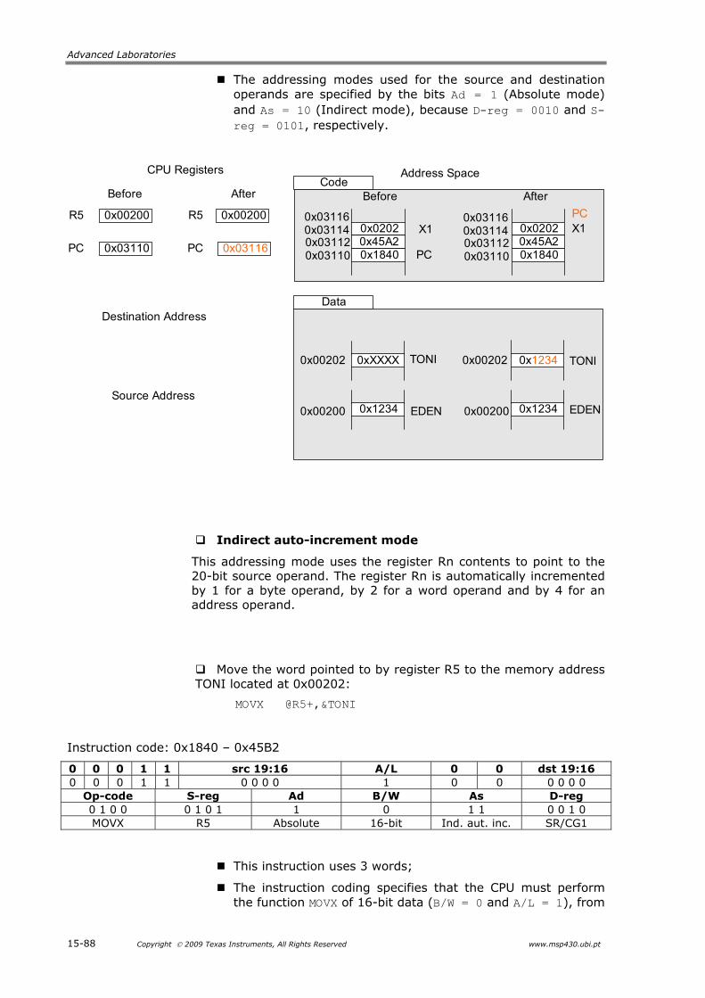
Advanced Laboratories
15-88 Copyright 2009 Texas Instruments, All Rights Reserved www.msp430.ubi.pt
The addressing modes used for the source and destination operands are specified by the bits Ad = 1 (Absolute mode) and As = 10 (Indirect mode), because D-reg = 0010 and S-reg = 0101, respectively.
Data
CPU Registers
Before After
0x00200R5 0x00200R5
Address Space
0x1234 0x1234EDEN0x00200 0x00200 EDEN
0xXXXX0x00202 0x12340x00202TONI TONI
0x02020x45A20x1840 PC
PC
Before AfterCode
X1 X1
Destination Address
Source Address
0x031100x031120x031140x03116
0x031100x031120x031140x03116
0x02020x45A20x1840
0x03110PC 0x03116PC
Indirect auto-increment mode
This addressing mode uses the register Rn contents to point to the 20-bit source operand. The register Rn is automatically incremented by 1 for a byte operand, by 2 for a word operand and by 4 for an address operand.
Move the word pointed to by register R5 to the memory address TONI located at 0x00202:
MOVX @R5+,&TONI
Instruction code: 0x1840 – 0x45B2
0 0 0 1 1 src 19:16 A/L 0 0 dst 19:16 0 0 0 1 1 0 0 0 0 1 0 0 0 0 0 0
Op-code S-reg Ad B/W As D-reg 0 1 0 0 0 1 0 1 1 0 1 1 0 0 1 0 MOVX R5 Absolute 16-bit Ind. aut. inc. SR/CG1
This instruction uses 3 words;
The instruction coding specifies that the CPU must perform the function MOVX of 16-bit data (B/W = 0 and A/L = 1), from
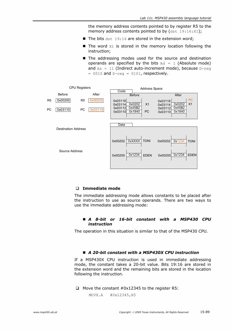
Lab 11c. MSP430 assembly language tutorial
www.msp430.ubi.pt Copyright 2009 Texas Instruments, All Rights Reserved 15-89
the memory address contents pointed to by register R5 to the memory address contents pointed to by (dst 19:16:X1);
The bits dst 19:16 are stored in the extension word;
The word X1 is stored in the memory location following the instruction;
The addressing modes used for the source and destination operands are specified by the bits Ad = 1 (Absolute mode) and As = 11 (Indirect auto-increment mode), because D-reg = 0010 and S-reg = 0101, respectively.
Data
CPU Registers
Before After
0x00200R5 0x00202R5
Address Space
0x1234 0x1234EDEN0x00200 0x00200 EDEN
0xXXXX0x00202 0x12340x00202TONI TONI
0x02020x45B20x1840 PC
PC
Before AfterCode
X1 X1
Destination Address
Source Address
0x031100x031120x031140x03116
0x031100x031120x031140x03116
0x02020x45B20x1840
0x03110PC 0x03116PC
Immediate mode
The immediate addressing mode allows constants to be placed after the instruction to use as source operands. There are two ways to use the immediate addressing mode:
A 8-bit or 16-bit constant with a MSP430 CPU instruction
The operation in this situation is similar to that of the MSP430 CPU.
A 20-bit constant with a MSP430X CPU instruction
If a MSP430X CPU instruction is used in immediate addressing mode, the constant takes a 20-bit value. Bits 19:16 are stored in the extension word and the remaining bits are stored in the location following the instruction.
Move the constant #0x12345 to the register R5:
MOVX.A #0x12345,R5
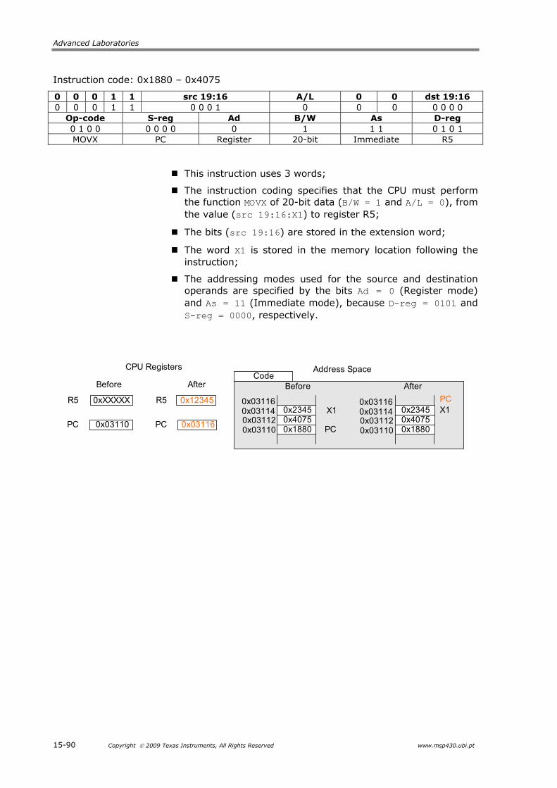
Advanced Laboratories
15-90 Copyright 2009 Texas Instruments, All Rights Reserved www.msp430.ubi.pt
Instruction code: 0x1880 – 0x4075
0 0 0 1 1 src 19:16 A/L 0 0 dst 19:16 0 0 0 1 1 0 0 0 1 0 0 0 0 0 0 0
Op-code S-reg Ad B/W As D-reg 0 1 0 0 0 0 0 0 0 1 1 1 0 1 0 1 MOVX PC Register 20-bit Immediate R5
This instruction uses 3 words;
The instruction coding specifies that the CPU must perform the function MOVX of 20-bit data (B/W = 1 and A/L = 0), from the value (src 19:16:X1) to register R5;
The bits (src 19:16) are stored in the extension word;
The word X1 is stored in the memory location following the instruction;
The addressing modes used for the source and destination operands are specified by the bits Ad = 0 (Register mode) and As = 11 (Immediate mode), because D-reg = 0101 and S-reg = 0000, respectively.
CPU Registers
Before After
0xXXXXXR5 0x12345R5
Address Space
0x23450x40750x1880 PC
PC
Before AfterCode
X1 X1
0x031100x031120x031140x03116
0x031100x031120x031140x03116
0x23450x40750x1880
0x03110PC 0x03116PC

Lab 11c. MSP430 assembly language tutorial
www.msp430.ubi.pt Copyright 2009 Texas Instruments, All Rights Reserved 15-91
15.3.3 Assembly language programming characteristics
The following section introduces some fundamentals of assembly language programming using the MSP430 family of microcontrollers. Rather than make an exhaustive study of programming methodologies and techniques, the intention is to focus on the aspects of assembly language programming relevant to the MSP430 family.
The examples are based on the MSP430 CPU, although they can also be applied to the MSP430X CPU. Where appropriate, differences between the MSP430 CPU and MSP430X CPU are highlighted.
Status system flags
Bit modification
The state of one or more bits of a value can be changed by the bit clear (BIC) and bit set (BIS) instructions, as described below.
The BIC instruction clears one or more bits of the destination operand. This is carried out by inverting the source value then performing a logical & (AND) operation with the destination. Therefore, if any bit of the source is one, then the corresponding bit of the destination will be cleared to zero.
BIC source,destination or BIC.W source,destination
BIC.B source,destination
Consider the instruction:
BIC #0x000C,R5
This clears bits 2 and 3 of register R5 to zero, leaving the remaining bits unchanged.
There is also the bit set (BIS) instruction:
BIS source,destination or BIS.W source,destination
BIS.B source,destination
This sets one or more bits of the destination using a similar procedure to the previous instruction. The instruction performs a logical | (OR) between the contents of the source and the destination.

Advanced Laboratories
15-92 Copyright 2009 Texas Instruments, All Rights Reserved www.msp430.ubi.pt
For example, the instruction:
BIS #0x000C,R5
Sets bits 2 and 3 of register R5, leaving the remaining bits unchanged.
It is recommended that whenever it is necessary to create control flags, that these are located in the least significant nibble of a word. In this case, the CPU constant generators can generate the constants necessary (1, 2, 4, 8) for bit operations. The code produced is more compact and therefore the execution will be faster.
CPU status bits modification
The CPU contains a set of flags in the Status Register (SR) that reflect the status of the CPU operation, for example that the previous instruction has produced a carry (C) or an overflow (V).
It is also possible to change the status of these flags directly through the execution of emulated instructions, which use the BIC and BIS instructions described above.
Directly changing the CPU status flags
The following instructions clear the CPU status flags (C, N and Z):
CLRC; clears carry flag (C). Emulated by BIC #1,SR
CLRN; clears negative flag (N). Emulated by BIC #4,SR
CLRZ; clears the zero flag (Z). Emulated by BIC #2,SR
The following instructions set the CPU status flags (C, N and Z):
SETC; set the carry flag (C). Emulated by BIS #1,SR
SETN; set the negative flag (N). Emulated by BIS #4,SR
SETZ; set the zero flag (Z). Emulated by BIS #2,SR
Lab 11c. MSP430 assembly language tutorial
www.msp430.ubi.pt Copyright 2009 Texas Instruments, All Rights Reserved 15-93
Enable/disable interrupts
Two other instructions allow the flag that enables or disables the interrupts to be changed. The global interrupt enable GIE flag of the register SR may be set to disable interrupts:
DINT; Disable interrupts. (emulated by BIC #8,SR)
or it may be cleared to enable interrupts:
EINT; Enable interrupts. (emulated by BIS #8,SR)
Arithmetic and logic operations
Addition and Subtraction
The MSP430 CPU has instructions that perform addition and subtraction operations, with and without the carry flag (C). It is also possible to perform addition operations of values represented in binary coded decimal (BCD) format.
Addition operations
There are three different instructions to carry out addition operations. The addition of two values is performed by the instruction:
ADD source,destination or ADD.W source,destination
ADD.B source,destination
The addition of two values, also taking into consideration the state of the carry bit (C), is performed by the instruction:
ADDC source,destination or ADDC.W source,destination
ADDC.B source,destination
The carry bit (C) itself can be added to a value using the instruction:
ADC destination or ADC.W destination
ADC.B destination
Advanced Laboratories
15-94 Copyright 2009 Texas Instruments, All Rights Reserved www.msp430.ubi.pt
The CPU status flags are updated to reflect the result of an operation.
For example, two 32-bit values are represented by the combination of registers R5:R4 and R7:R6, where the format is most significant word: least significant word.
The addition operation must propagate the carry from the addition of the least significant register words (R4 and R6) to the addition of the most significant words (R5 and R7).
MOV #0x1234,R5 ; operand 1 most significant word
MOV #0xABCD,R4 ; operand 1 least significant word
MOV #0x1234,R7 ; operand 2 most significant word
MOV #0xABCD,R6 ; operand 2 least significant word
ADD R4,R6 ; add least significant words
ADDC R5,R7 ; add most significant words with carry
The code begins by loading the values into the registers to be added, 0x1234ABCD in R5:R4 and 0x1234ABCD in R7:R6.
The operation continues by adding the two least significant words 0xABCD and 0xABCD in registers R4 and R6. The addition may change the carry bit (C), and this must be taken into account during the addition of the two most significant words. The result is placed in the structure formed by the registers R7:R6.
Subtraction operations
There are three instructions to perform subtraction operations. The subtraction of two values is performed by the instruction:
SUB source,destination or SUB.W source,destination
SUB.B source,destination
The subtraction of two values, taking into consideration the carry bit (C), is performed by the instruction:
SUBC source,destination or SUBC.W source,destination
SUBC.B source,destination

Lab 11c. MSP430 assembly language tutorial
www.msp430.ubi.pt Copyright 2009 Texas Instruments, All Rights Reserved 15-95
The subtraction of destination taking into consideration the carry bit (C) is provided by the instruction:
SBC destination or SBC.W destination
SBC.B destination
The CPU status flags are updated to reflect the result of the operation.
The borrow is treated as a .NOT. carry: The carry is set to 1 if NO borrow, and reset if borrow.
For example, two 32-bit values are represented by the combination of registers R5:R4 and R7:R6, where the format is most significant word:least significant word.
The subtraction operation of these values must propagate the carry (C) from the subtraction of the least significant words (R4 and R6) to the most significant words (R5 to R7).
Two 32-bit values are subtracted in the example presented below:
MOV #0xABCD,R5 ; load operand 1 in R5:R4
MOV #0x1234,R4
MOV #0x0000,R7 ; load operand 2 in R7:R6
MOV #0x1234,R6
SUB R4,R6 ; subtract least significant words
SUBC R5,R7 ; subtract most significant words
; with carry
The code begins by loading the values in the registers to be subtracted, 0xABCD1234 into R5:R4 and 0x00001234 into R7:R6. The next operation is to subtract the two least significant words. The result of the subtraction affects the carry bit (C), which must be taken into account during the subtraction of the two most significant words.

Advanced Laboratories
15-96 Copyright 2009 Texas Instruments, All Rights Reserved www.msp430.ubi.pt
BCD format addition
The CPU supports addition operations for values represented in binary coded decimal (BCD) format. There are two instructions to perform addition operations in this format:
DADD source,destination or DADD.W source,destination
DADD.B source,destination
The addition of the carry bit (C) to a BCD value is provided by instruction:
DADC destination or DADC.W destination
DADC.B destination
The CPU status flags are updated to reflect the result of the operation.
For example, two 32-bit BCD values are represented by the combination of registers R5:R4 and R7:R6, where the format is most significant word:least significant word. The addition of these values must propagate the carry from the addition of the least significant words (R4 and R6) to the addition of the most significant words (R5 and R7).
Two 32-bit BCD values are added in the example below:
MOV #0x1234,R5 ; operand 1 most significant word
MOV #0x5678,R4 ; operand 1 least significant word
MOV #0x1234,R7 ; operand 2 most significant word
MOV #0x5678,R6 ; operand 2 least significant word
CLRC ; clear carry flag, C
DADD R4,R6 ; add least significant words
DADD R5,R7 ; add most significant words
The code begins by loading the BCD values into the registers to be added. The carry flag (C) is cleared. Next, the least significant words are added together. The result of the addition generates a carry, which must be added together with the two most significant words.
Lab 11c. MSP430 assembly language tutorial
www.msp430.ubi.pt Copyright 2009 Texas Instruments, All Rights Reserved 15-97
Sign extension
The CPU supports 8-bit and 16-bit operations. Therefore, the CPU needs to be able to extend the sign of a 8-bit value to a 16-bit format.
The extension of the sign bit is produced by the instruction:
SXT destination
For example, the sign extension of the value contained in R5 is:
MOV.B #0xFC,R5 ; place the value 0xFC in R5
SXT R5 ; sign extend word. R5 = 0xFFFC
Increment and decrement operations
There are several operations that need to increment or decrement a value, e.g. control of the number of code iterations (for or while loops), access to memory blocks using pointers etc. Therefore, there are four emulated instructions based on the ADD instruction, which facilitate the implementation of these operations.
To increment a value by one:
INC destination or INC.W destination
INC.B destination
Similarly, to decrement a value by one:
DEC destination or DEC.W destination
DEC.B destination
In the following example, the value placed in R5 is initially incremented and then decremented:
MOV.B #0x00,R5 ; move 0x00 to register R5
INC R5 ; increment R5 by one. R5 = 0x0001
DEC R5 ; decrement R5 by one. R5 = 0x0000
Advanced Laboratories
15-98 Copyright 2009 Texas Instruments, All Rights Reserved www.msp430.ubi.pt
The ability of the CPU to address 16-bit values requires the ability to increment or decrement the address pointer by two. The following instruction is used to increment a value by two:
INCD destination or INCD.W destination
INCD.B destination
Similarly, to decrement a value by two, the following instruction is used:
DECD destination or DECD.W destination
DECD.B destination
The CPU status flags are updated to reflect the result of the operation.
In the following example, the value stored in register R5 is initially incremented by two and then decremented by two:
MOV.B #0x00,R5 ; move 0x00 to the register R5
INCD R5 ; Increment R5 by two. R5 = 0x0002
DECD R5 ; Decrement R5 by two. R5 = 0x0000
Logical operations
Logic instructions
The CPU performs a set of logical operations through the operations AND (logical and), XOR (exclusive OR) and INV (invert). The CPU status flags are updated to reflect the result of the operation.
The AND logical operation between two operands is performed by the instruction:
AND source,destination or AND.W source,destination
AND.B source,destination
In the following example, the value 0xFF is moved to the register R4, and the value 0x0C is moved to the register R5. A logical AND logic operation is performed between these two registers, putting the result in register R5:

Lab 11c. MSP430 assembly language tutorial
www.msp430.ubi.pt Copyright 2009 Texas Instruments, All Rights Reserved 15-99
MOV.B #0xFF,R4 ; load operand 1 into R4
MOV.B #0x0C,R5 ; load operand 2 into R5
AND.B R4,R5 ; result of AND located in R5
The code begins by loading the operands into registers R4 and R5. The result of the logical operation between the two registers is placed in register R5. For the MSP430X the bits 19:8 of the result register take the value zero.
The XOR logical operation between two operands is performed by the instruction:
XOR source,destination or XOR.W source,destination
XOR.B source,destination
In the following example, the value 0xFF is moved to the register R4, and the value 0x0C is moved to the register R5. The logical XOR operation is performed between the two registers, putting the result in register R5:
MOV.B #0x00FF,R4 ; load operand 1 into R4
MOV.B #0x000C,R5 ; load operand 1 into R5
XOR.B R4,R5 ; XOR result located in R5
The NOT logical operation between two operands is performed by the INV (invert) instruction:
INV destination or INV.W destination
INV.B destination
The XOR logic operation between two operands was performed in the previous example. The following example demonstrates a way to implement a logical OR. The code begins by loading the operands into registers R4 and R5. The contents of the registers are inverted, then the logical & (AND) operation is performed between them.
MOV #0x1100,R4 ; load operand 1 into R4
MOV #0x1010,R5 ; load operand 2 into R5
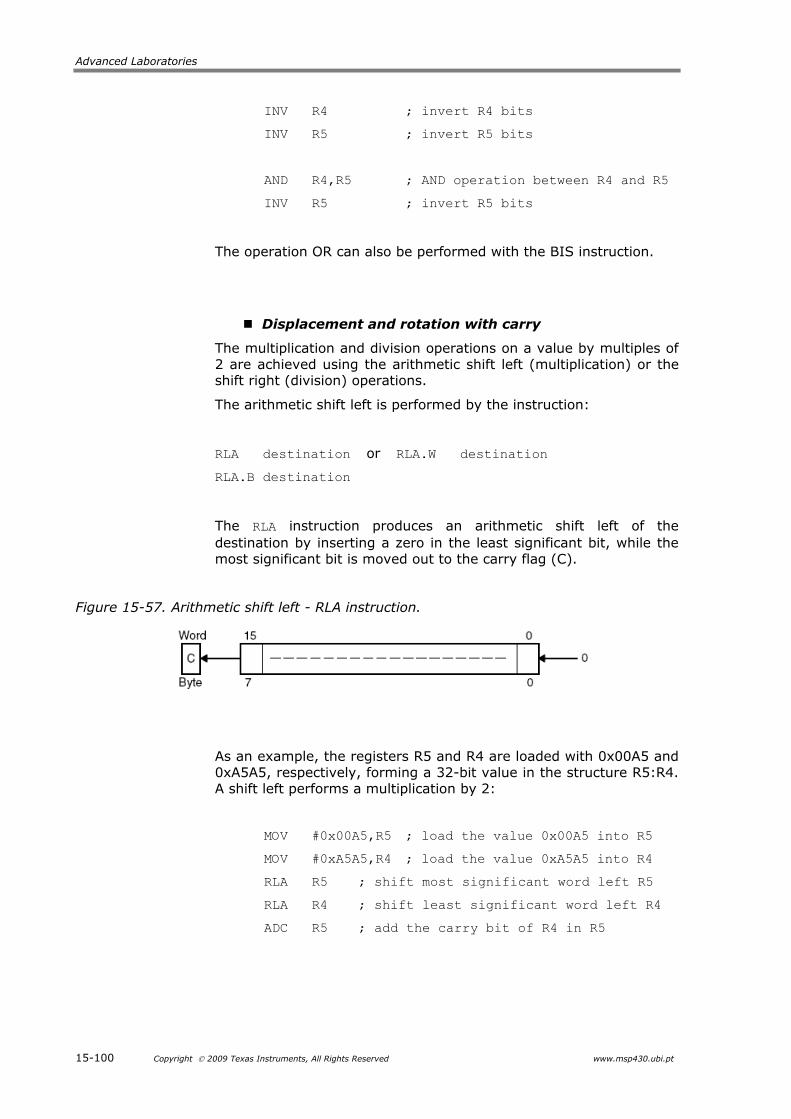
Advanced Laboratories
15-100 Copyright 2009 Texas Instruments, All Rights Reserved www.msp430.ubi.pt
INV R4 ; invert R4 bits
INV R5 ; invert R5 bits
AND R4,R5 ; AND operation between R4 and R5
INV R5 ; invert R5 bits
The operation OR can also be performed with the BIS instruction.
Displacement and rotation with carry
The multiplication and division operations on a value by multiples of 2 are achieved using the arithmetic shift left (multiplication) or the shift right (division) operations.
The arithmetic shift left is performed by the instruction:
RLA destination or RLA.W destination
RLA.B destination
The RLA instruction produces an arithmetic shift left of the destination by inserting a zero in the least significant bit, while the most significant bit is moved out to the carry flag (C).
Figure 15-57. Arithmetic shift left - RLA instruction.
As an example, the registers R5 and R4 are loaded with 0x00A5 and 0xA5A5, respectively, forming a 32-bit value in the structure R5:R4. A shift left performs a multiplication by 2:
MOV #0x00A5,R5 ; load the value 0x00A5 into R5
MOV #0xA5A5,R4 ; load the value 0xA5A5 into R4
RLA R5 ; shift most significant word left R5
RLA R4 ; shift least significant word left R4
ADC R5 ; add the carry bit of R4 in R5
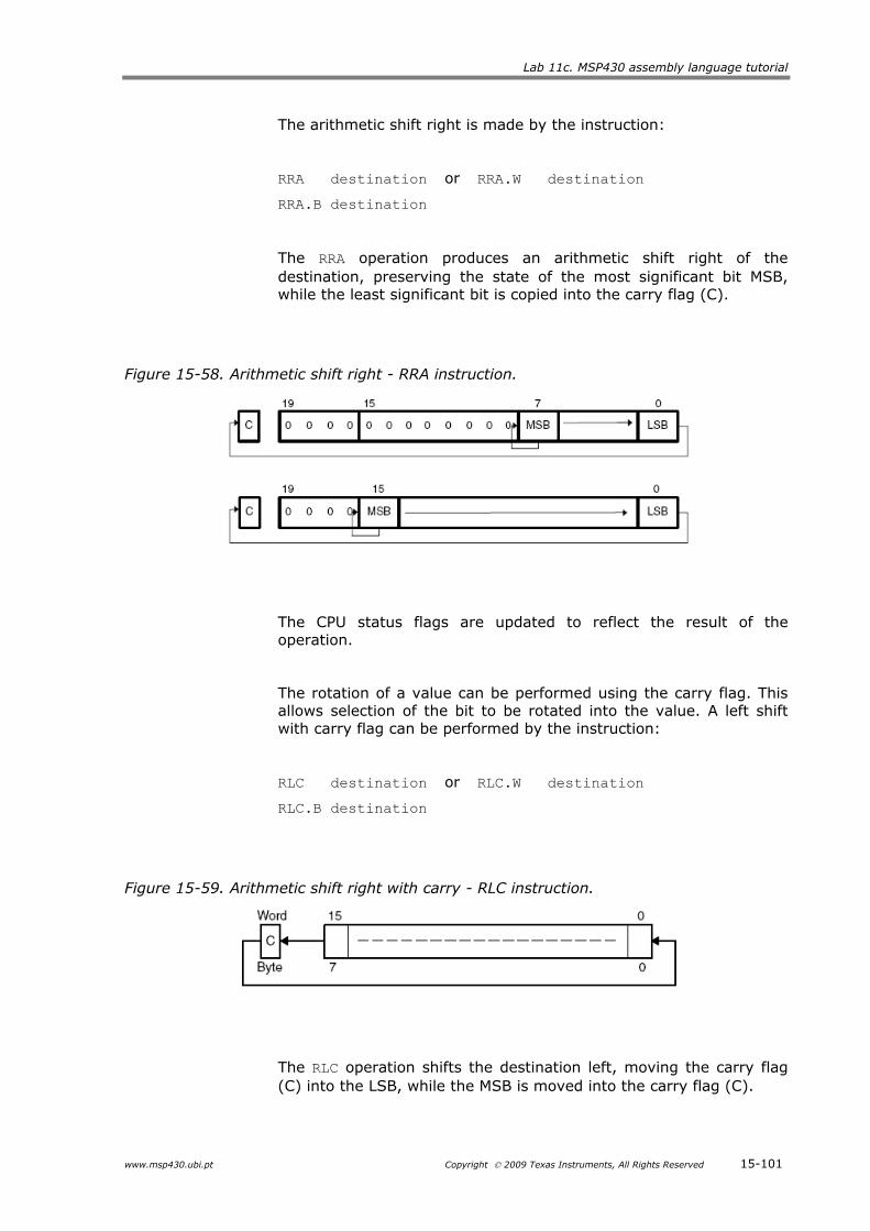
Lab 11c. MSP430 assembly language tutorial
www.msp430.ubi.pt Copyright 2009 Texas Instruments, All Rights Reserved 15-101
The arithmetic shift right is made by the instruction:
RRA destination or RRA.W destination
RRA.B destination
The RRA operation produces an arithmetic shift right of the destination, preserving the state of the most significant bit MSB, while the least significant bit is copied into the carry flag (C).
Figure 15-58. Arithmetic shift right - RRA instruction.
The CPU status flags are updated to reflect the result of the operation.
The rotation of a value can be performed using the carry flag. This allows selection of the bit to be rotated into the value. A left shift with carry flag can be performed by the instruction:
RLC destination or RLC.W destination
RLC.B destination
Figure 15-59. Arithmetic shift right with carry - RLC instruction.
The RLC operation shifts the destination left, moving the carry flag (C) into the LSB, while the MSB is moved into the carry flag (C).

Advanced Laboratories
15-102 Copyright 2009 Texas Instruments, All Rights Reserved www.msp430.ubi.pt
The RRC operation shifts the destination right, moving the carry flag (C) into the MSB, and the LSB is moved to the carry flag (C).
RRC destination or RRC.W destination
RRC.B destination
Figure 15-60. Rotate right through carry destination word - RRC instruction.
In the following example, the register pair R4:R5 are loaded with 0x0000 and 0xA5A5, respectively, forming a 32-bit value. A shift left of R4:R5 multiplies the value by 2. This example is similar to the previous one, but requires one less instruction:
MOV #0x0000,R4 ; load R4 with #0x0000
MOV #0xA5A5,R5 ; load R5 with #0xA5A5
RLA R5 ; Rotate least significant word left
RLC R4 ; Rotate most significant word left
Byte exchange
To swap the destination bytes contents of a 16-bit register, the following instruction is used:
SWPB destination
The operation has no effect on the state of the CPU flags;
In the following example, the bytes of register R5 are exchanged:
MOV #0x1234,R5 ; move the value 0x1234 to R5
SWPB R5 ; exchange the LSB with the MSB. R5 = 0x3412
The above instruction sequence starts by loading the value 0x1234 into the register R5, followed by exchanging the contents of the LSB and the MSB of register R5.

Lab 11c. MSP430 assembly language tutorial
www.msp430.ubi.pt Copyright 2009 Texas Instruments, All Rights Reserved 15-103
Special operations with MSP430X CPU
In addition to MSP430 CPU instructions, the MPS430 CPU has a 20-bit memory address space and an instruction set that can optimize the performance of certain operations. We shall look at some of them now.
Repetition of an instruction
An MP430X CPU instruction, provided that it is used in Register addressing mode, can be repeated a preset number of times, up to a maximum of 15 times. It uses the instruction:
RPT #n ; repeat n times
RPT Rn ; repeat Rn.3:0 times
In the following example, the instruction sequence starts by loading the value 0x05AD into register R5. The CPU is informed that it must repeat the arithmetic shift left instruction 3 times. The resulting value in register R5 is the original value multiplied by 8.
MOV #0x05AD,R5
RPT #3
RLAX R5
Successive arithmetic shifts and shifts with carry flag (C)
The MSP430X CPU has an instruction set that allows a number of arithmetic shifts or shifts with carry to be carried out. Up to a maximum of 4 shifts can be performed on a 16-bit or 20-bit value.
To perform #n shifts right of a register with the carry flag, the following instruction is used:
RRCM #n,Rdst or RRCM.W #n,Rdst
RRCM.A #n,Rdst

Advanced Laboratories
15-104 Copyright 2009 Texas Instruments, All Rights Reserved www.msp430.ubi.pt
Figure 15-61. Sucessive arithmetic shift right with carry - RRCM instruction.
If this is a 16-bit operation, bits 19:16 of the register are reset to zero. The Carry (C) flag contents are placed in the MSB, while the LSB is copied into the carry flag.
To perform an unsigned #n shifts right of a register, the following instruction is used:
RRUM #n,Rdst or RRUM.W #n,Rdst
RRUM.A #n,Rdst
Figure 15-62. Successive arithmetic unsigned shift right with carry - RRUM instruction.
If this is a 16-bit operation, then bits 19:16 of the register are reset to zero. The MSB of the register is cleared to zero and the LSB is copied to the carry (C) flag.
To perform a #n arithmetic shift right using a register, the following instruction is used:
RRAM #n,Rdst or RRAM.W #n,Rdst
RRAM.A #n,Rdst
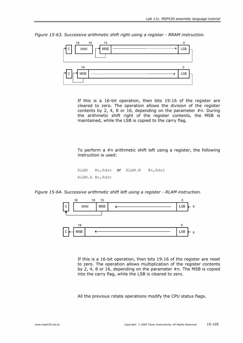
Lab 11c. MSP430 assembly language tutorial
www.msp430.ubi.pt Copyright 2009 Texas Instruments, All Rights Reserved 15-105
Figure 15-63. Successive arithmetic shift right using a register - RRAM instruction.
If this is a 16-bit operation, then bits 19:16 of the register are cleared to zero. The operation allows the division of the register contents by 2, 4, 8 or 16, depending on the parameter #n. During the arithmetic shift right of the register contents, the MSB is maintained, while the LSB is copied to the carry flag.
To perform a #n arithmetic shift left using a register, the following instruction is used:
RLAM #n,Rdst or RLAM.W #n,Rdst
RLAM.A #n,Rdst
Figure 15-64. Successive arithmetic shift left using a register - RLAM instruction.
If this is a 16-bit operation, then bits 19:16 of the register are reset to zero. The operation allows multiplication of the register contents by 2, 4, 8 or 16, depending on the parameter #n. The MSB is copied into the carry flag, while the LSB is cleared to zero.
All the previous rotate operations modify the CPU status flags.

Advanced Laboratories
15-106 Copyright 2009 Texas Instruments, All Rights Reserved www.msp430.ubi.pt
In the following example, the value 0x1234 is multiplied by 1.25:
MOV #0x1234,R4 ;load 0x1234 in R4
MOV R4,R5 ;store R4 in R5
RRAM #2,R4 ; R4 = 0.25*R4
ADD R4,R5 ; R5 = 1.25*R4
20-bit addressing instructions
The addressing instructions can use the 20-bit addresses. There is the limitation that with the exception of the instruction MOVA, only Register and Immediate addressing modes can be used.
A 20-bit address can be manipulated using operations: addition (ADDA), subtraction (SUBA), double-increment (INCDA) and double-decrement (DECDA). There are other instructions of this type, which will be examined later. The contents of a register can be cleared by the instruction (CLRA). Finally, a 20-bit operand can be moved using the instruction (MOVA).
Program flow control
MSP430 CPU testing
Bit testing
Bit testing can be used to control program flow. Hence, the CPU provides an instruction to test the state of individual or multiple bits. The operation performs a logical & (AND) logical operation between the source and destination operands. The result is ignored and none of the operands are changed. This task is performed by the following instruction:
BIT source,destination or BIT.W source,destination
BIT.B source,destination
As a result of the operation, the CPU state flags are updated:
V: reset;
N: set if the MSB of the result is 1, otherwise reset;
Z: set if the result is zero, otherwise reset;
C: set if the result is not zero, otherwise reset.

Lab 11c. MSP430 assembly language tutorial
www.msp430.ubi.pt Copyright 2009 Texas Instruments, All Rights Reserved 15-107
For example, to test if bit R5.7 is set:
MOV #0x00CC,R5 ; load the value #0x00CC to R5
BIT #0x0080,R5 ; test R5.7
The result of the logical AND operation with 0x0080, the bit R5.7 is tested. Reasoning this case, the result modifies the flags (V = 0, N = 0, Z = 0, C = 1).
Comparison with zero
Another operation typically used in a program is the comparison of a value with zero, to determine if the value has reached zero. This operation is performed using the following emulated instruction:
TST source,destination or TST.W source,destination
TST.B source,destination
As a result of the operation, the CPU state flags are updated:
V: reset;
N: set if the MSB of the result is 1, otherwise reset;
Z: set if the result is zero, otherwise reset;
C: set.
For example, to test if register R5 is zero:
MOV #0x00CC,R5 ; move the value #0x00CC to R5
TST R5 ; test R5
The comparison of the register R5 with #0x0000 modifies the flags (V = 0, N = 0, Z = 0, C = 1).
Value comparison
Two operands can be compared using the instruction:
CMP source,destination or CMP.W source,destination
CMP.B source,destination

Advanced Laboratories
15-108 Copyright 2009 Texas Instruments, All Rights Reserved www.msp430.ubi.pt
The comparison result modifies the CPU status flags:
V: set if an overflow occurs;
N: set if the result is negative, otherwise reset (source >= destination);
Z: set if the result is zero, otherwise reset (source = destination);
C: set if there is a carry, otherwise reset (source <= destination).
In the following example, the contents of register R5 are compared with the contents of register R4:
MOV #0x0012,R5 ; move the value 0x0012 to R5
MOV #0x0014,R4 ; move the value 0x0014 to R4
CMP R4,R5
The register comparison modifies the CPU status flags (V = 0, N = 1, Z = 0, C = 0).
Program flow branch
A branch in program flow without any constraint is performed by the instruction:
BR destination
This instruction execution is only able to reach addresses in the address space below 64 kB. For addresses above this address space, the MSP430X CPU provides the instruction:
BRA destination
Each of the addressing modes can be used. For example:
BR #EXEC ;Branch to label EXEC or direct branch
;(e.g. #0A4h)
; Core instruction MOV @PC+,PC
BR EXEC ; Branch to the address contained in
; EXEC
; Core instruction MOV X(PC),PC
; Indirect address
BR &EXEC ; Branch to the address contained in

Lab 11c. MSP430 assembly language tutorial
www.msp430.ubi.pt Copyright 2009 Texas Instruments, All Rights Reserved 15-109
; absolute address EXEC
; Core instruction MOV X(0),PC
; Indirect address
BR R5 ; Branch to the address contained in R5
; Core instruction MOV R5,PC
; Indirect R5
BR @R5 ; Branch to the address contained in
; the word pointed to by R5.
; Core instruction MOV @R5,PC
; Indirect, indirect R5
BR @R5+ ; Branch to the address contained in
; the word pointed to by R5 and
; increment pointer in R5 afterwards.
; The next time—S/W flow uses R5
; pointer—it can alter program
; execution by access the next
; address in the table pointed to by R5
; Core instruction MOV @R5,PC
; Indirect, indirect R5 with
; autoincrement
BR X(R5) ; Branch to the address contained in
; the address pointed to by R5 + X
; (e.g. table with address starting at
; X). X can be an address or a label
; Core instruction MOV X(R5),PC
; Indirect, indirect R5 + X
In addition to the previous instructions it is possible to jump to a destination in the range +512 to -511 words using the instruction:
JMP destination
Conditional jump
Action can be taken depending on the values of the CPU status flags. Using the result of a previous operation, it is possible to produce jumps in the program flow execution. The new memory address must be in the range +512 to -511 words.
The following instructions are available for conditional jumps:
Advanced Laboratories
15-110 Copyright 2009 Texas Instruments, All Rights Reserved www.msp430.ubi.pt
Jump if equal (Z = 1):
JEQ destination or JZ destination
label1:
MOV 0x0100,R5
MOV 0x0100,R4
CMP R4,R5
JEQ label1
The above example compares the register R4 and R5 contents. As they are equal, the flag Z is set, and therefore, the jump to position label1 is executed.
Jump if different (Z = 0):
JNE destination or JNZ destination
label2:
MOV #0x0100,R5
MOV #0x0100,R4
CMP R4,R5
JNZ label2
The above example compares the contents of registers R4 and R5. As they are equal, the flag Z is set, and therefore, the jump to position label2 is not executed.
Jump if higher or equal (C = 1) – without sign:
JC destination or JHS destination
label3:
MOV #0x0100,R5
BIT #0x0100,R5
JC label3
The above example tests the state of bit R5.8. As this bit is set, the flag C is set, and therefore, the jump to position label3 is executed.

Lab 11c. MSP430 assembly language tutorial
www.msp430.ubi.pt Copyright 2009 Texas Instruments, All Rights Reserved 15-111
Jump if lower (C = 0) – without sign:
JNC destination or JLO destination
label4:
MOV #0x0100,R5
BIT #0x0100,R5
JNC label4
The above example tests the state of bit R5.8. As it is set, the flag C is set, and therefore, the jump to position label4 is not executed.
Jump if higher or equal (N = 0 and V = 0) or (N = 1 and V = 1) – with sign:
JGE destination
label5:
MOV #0x0100,R5
CMP #0x0100,R5
JGE label5
The above example compares the contents of register R5 with the constant #0x0100. As they are equal, both flags N and V are reset, and therefore, the jump to the address label5 is executed.
Jump if lower (N = 1 and V = 0) or (N = 0 and V = 1) – with sign:
JL destination
label6:
MOV #0x0100,R5
CMP #0x0100,R5
JL label6
The above example compares the contents of register R5 with the constant #0x0100. As they are equal, both flags N and V are reset, and therefore, the jump to the address label6 is not executed.
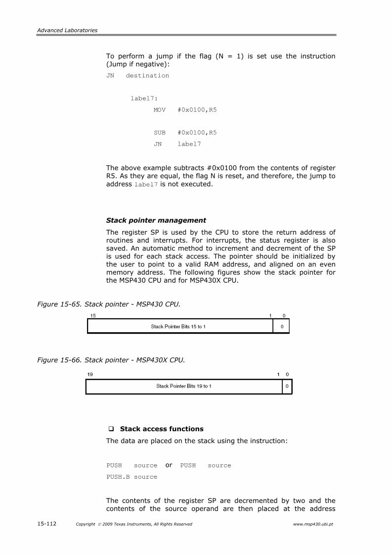
Advanced Laboratories
15-112 Copyright 2009 Texas Instruments, All Rights Reserved www.msp430.ubi.pt
To perform a jump if the flag (N = 1) is set use the instruction (Jump if negative):
JN destination
label7:
MOV #0x0100,R5
SUB #0x0100,R5
JN label7
The above example subtracts #0x0100 from the contents of register R5. As they are equal, the flag N is reset, and therefore, the jump to address label7 is not executed.
Stack pointer management
The register SP is used by the CPU to store the return address of routines and interrupts. For interrupts, the status register is also saved. An automatic method to increment and decrement of the SP is used for each stack access. The pointer should be initialized by the user to point to a valid RAM address, and aligned on an even memory address. The following figures show the stack pointer for the MSP430 CPU and for MSP430X CPU.
Figure 15-65. Stack pointer - MSP430 CPU.
Figure 15-66. Stack pointer - MSP430X CPU.
Stack access functions
The data are placed on the stack using the instruction:
PUSH source or PUSH source
PUSH.B source
The contents of the register SP are decremented by two and the contents of the source operand are then placed at the address
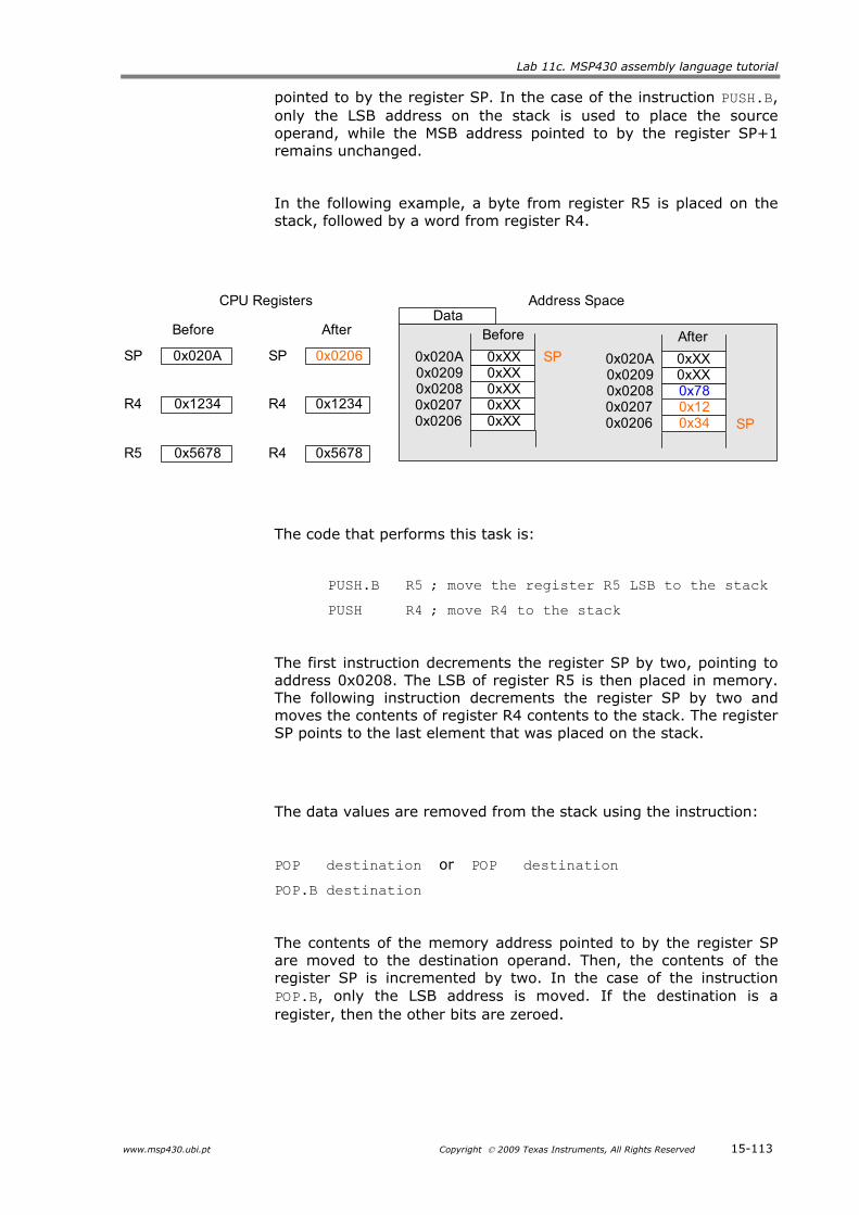
Lab 11c. MSP430 assembly language tutorial
www.msp430.ubi.pt Copyright 2009 Texas Instruments, All Rights Reserved 15-113
pointed to by the register SP. In the case of the instruction PUSH.B, only the LSB address on the stack is used to place the source operand, while the MSB address pointed to by the register SP+1 remains unchanged.
In the following example, a byte from register R5 is placed on the stack, followed by a word from register R4.
CPU Registers
Before After
Address Space
0xXX SP
Before After
Data
0x02060x0207
0xXX0xXX0xXX0x0208
0x02090x020A
0xXX0x020ASP 0x0206SP
0x1234R4 0x1234R4
0xXX
SP0x02060x0207
0x340x120x780x0208
0x02090x020A
0xXX
0x5678R5 0x5678R4
The code that performs this task is:
PUSH.B R5 ; move the register R5 LSB to the stack
PUSH R4 ; move R4 to the stack
The first instruction decrements the register SP by two, pointing to address 0x0208. The LSB of register R5 is then placed in memory. The following instruction decrements the register SP by two and moves the contents of register R4 contents to the stack. The register SP points to the last element that was placed on the stack.
The data values are removed from the stack using the instruction:
POP destination or POP destination
POP.B destination
The contents of the memory address pointed to by the register SP are moved to the destination operand. Then, the contents of the register SP is incremented by two. In the case of the instruction POP.B, only the LSB address is moved. If the destination is a register, then the other bits are zeroed.

Advanced Laboratories
15-114 Copyright 2009 Texas Instruments, All Rights Reserved www.msp430.ubi.pt
CPU Registers
Before After
Address Space
0xXX
SP
Before After
Data
0x02060x0207
0x340x120x780x0208
0x02090x020A
0xXX0x0206SP 0x020ASP
0xXXXXR4 0x1234R4
0xXX SP
0x02060x0207
0x340x120x780x0208
0x02090x020A
0xXX
0xXXXXR5 0x0078R4
The code that performs this task is:
POP R4 ; extract a word from the stack
POP.B R5 ; extract a byte from the stack
The instruction POP R4 extracts the word pointed to by the register SP and places it in register R4. Then, the stack pointer is incremented by two, to point to the memory address 0x0208. The instruction POP.B R5 moves the byte pointed to by the register SP to register R5. The stack pointer is then incremented by two, to point to the memory address 0x020A. The register SP points to the last element that was placed on the stack, but not yet retrieved.
In addition to 8-bit or 16-bit values, the MSP430X CPU provides instructions with the ability to handle 20-bit data in memory. This usually requires two words to be placed on the stack.
The placing of 20-bit data on the stack is performed by the instruction:
PUSHX.A source
The register SP is decremented by 4 and the source address operand is placed on the stack. The following figure shows the use of this instruction:

Lab 11c. MSP430 assembly language tutorial
www.msp430.ubi.pt Copyright 2009 Texas Instruments, All Rights Reserved 15-115
CPU Registers
Before After
Address Space
0xXX
0xXX
SP
Before After
Data
0x002050x002060x00207
0xXX0xXX0xXX0x00208
0x002090x0020A
0xXX0x0020ASP 0x00206SP
0x12345R4 0x12345R4
0xXX
0xXXSP
0x002050x002060x00207
0x450x230x010x00208
0x002090x0020A
0xXX
The code that performs this task is:
PUSHX.A R4 ; place the 20-bits address of
; register R4 on the stack
The MSP430X CPU has the following instruction available for removing a 20-bit data value from the stack:
POPX.A destination
This instruction moves the 20-bit value pointed to by the register SP from the stack to the destination register. Then, the register SP is incremented by 4. The following figure shows the use of this instruction:
CPU Registers
Before After
Address SpaceData
0x0020ASP 0x00206SP
0xXXXXXR4 0x12345R4
Before
0xXX
0xXXSP
0x002050x002060x00207
0x450x230x010x00208
0x002090x0020A
0xXXSP
After
0x002050x002060x002070x002080x002090x0020A 0xXX
0xXX0x450x230x010xXX
The code that performs this task is:
POPX.A R4 ; extract the 20-bits address from stack
; to the register R4
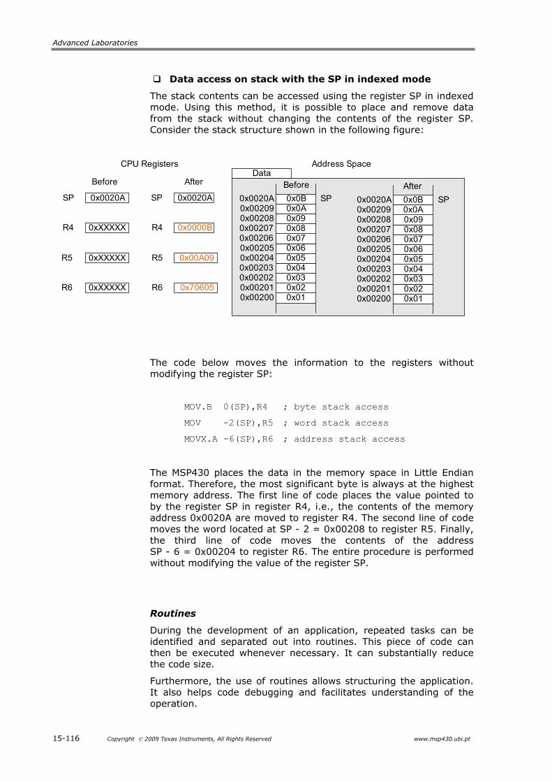
Advanced Laboratories
15-116 Copyright 2009 Texas Instruments, All Rights Reserved www.msp430.ubi.pt
Data access on stack with the SP in indexed mode
The stack contents can be accessed using the register SP in indexed mode. Using this method, it is possible to place and remove data from the stack without changing the contents of the register SP. Consider the stack structure shown in the following figure:
CPU Registers
Before After
Address Space
0x0B
0x06
0x01
SP
Before After
Data
0x002040x002050x002060x00207
0x002000x002010x002020x00203
0x020x030x040x05
0x070x080x090x00208
0x002090x0020A
0x0A0x0020ASP 0x0020ASP
0xXXXXXR4 0x0000BR4
0xXXXXXR5 0x00A09R5
0xXXXXXR6 0x70605R6
0x0B
0x06
0x01
SP
0x002040x002050x002060x00207
0x002000x002010x002020x00203
0x020x030x040x05
0x070x080x090x00208
0x002090x0020A
0x0A
The code below moves the information to the registers without modifying the register SP:
MOV.B 0(SP),R4 ; byte stack access
MOV -2(SP),R5 ; word stack access
MOVX.A -6(SP),R6 ; address stack access
The MSP430 places the data in the memory space in Little Endian format. Therefore, the most significant byte is always at the highest memory address. The first line of code places the value pointed to by the register SP in register R4, i.e., the contents of the memory address 0x0020A are moved to register R4. The second line of code moves the word located at SP - 2 = 0x00208 to register R5. Finally, the third line of code moves the contents of the address SP - 6 = 0x00204 to register R6. The entire procedure is performed without modifying the value of the register SP.
Routines
During the development of an application, repeated tasks can be identified and separated out into routines. This piece of code can then be executed whenever necessary. It can substantially reduce the code size.
Furthermore, the use of routines allows structuring the application. It also helps code debugging and facilitates understanding of the operation.

Lab 11c. MSP430 assembly language tutorial
www.msp430.ubi.pt Copyright 2009 Texas Instruments, All Rights Reserved 15-117
Invoking a routine
A routine is identified by a label in assembly language. A routine call is made at the point in the program where execution must be changed to perform a task. When the task is complete, it is necessary to return to the point just after where the routine call was called.
Two different instructions are available to perform the routine call, namely CALL and CALLA.
The following instruction can be used if the routine is located in the address below 64 kB:
CALL destination
This instruction decrements the register SP by two, to store the return address. The register PC is then loaded with the routine address and the routine executed. The CALL instruction can be used with any of the addressing modes. The return is performed by the instruction RET.
In MSP430X CPU is also available the instruction:
CALLA destination
This instruction decrements the register SP by four to store the return address. The register PC is then loaded with the routine address. The return is performed by the instruction RETA.
Routine return
The routine execution return depends on the call type that was used. If the routine is called using a instruction CALL, the following instruction must be used to return:
RET
This instruction extracts the value pointed to by the register SP and places it in the PC.
If the routine call was made with the instruction CALLA, then the following instruction should be used to return:
RETA

Advanced Laboratories
15-118 Copyright 2009 Texas Instruments, All Rights Reserved www.msp430.ubi.pt
Passing parameters to the routine
There are two different ways to move data to a routine.
The first makes use of a register. The data values needed for the routine execution are placed in pre-defined registers before the routine call. The return from the routine execution can use a similar method.
The second method makes use of the stack. The parameters necessary to execute the routine are placed on the stack using the PUSH or PUSHX instructions.
The routine can use any of the methods already discussed to access the information.
To return from the routine, the stack can again be used to pass the parameters, using a POP instruction.
Care is needed in the use of this method to avoid stack overflow problems. Generally, the stack pointer must set back to the value just before pushing parameters after execution of the routine.
Routine examples
The following examples bring together the concepts mentioned in this section.
In the first example, the routine is in the address space below 64 kB. Therefore, the instruction CALL is used to call the routine. The parameters are passed to the routine through registers:
;--------------------
; Routine
;--------------------
adder:
ADD R4,R5
RET ; return from routine
;--------------------
; Main
;--------------------
MOV &var1,R4 ; parameter var1 in R4
MOV &var2,R5 ; parameter var2 in R5
CALL #adder ; call routine adder
MOV R5,&var3 ; result R5 in var3

Lab 11c. MSP430 assembly language tutorial
www.msp430.ubi.pt Copyright 2009 Texas Instruments, All Rights Reserved 15-119
In the second example, the routine is the address space above 64 kB. Therefore, the instruction CALLA is used to call the routine. The parameters are passed to the routine by placing values on the stack.
;--------------------
; Routine
;--------------------
adder:
MOV 4(SP),R4 ; get var2 from stack
MOV 6(SP),R5 ; get var1 from stack
ADD R4,R5
MOV R5,6(SP) ; place the result on stack
RETA ; return from stack
;--------------------
; Main
;--------------------
PUSH.W &var1 ; place var1 on stack
PUSH.W &var2 ; place var2 on stack
CALLA #adder ; call routine adder
ADD #2,SP ; point SP
POP &var3 ; extract result to var3
Interrupts
Stack management during an interrupt
During an interrupt, the PC and SR registers are automatically placed on the stack as in the figures shown below. The following figures show the interrupt processing for the MSP430 CPU and MSP430X CPU.

Advanced Laboratories
15-120 Copyright 2009 Texas Instruments, All Rights Reserved www.msp430.ubi.pt
Figure 15-67. Interrupt processing - MSP430 CPU.
Figure 15-68. Interrupt processing - MSP430X CPU.
When the instruction RETI is executed, the PC and SR registers are restored thus enabling the return to the program execution point before the interrupt occurred.
An important aspect consists of modifying the low power mode in which the device was before the interrupt. As the register SR is restored at the end of the interrupt, its contents stored on the stack can be modified prior to execution of the RETI instruction. Thus, an new operation mode will be used. For example, executing the instruction:
BIC #00F0,0(SP) ; clear bits CPUOFF, OSCOFF, SCG0 and
; SCG1
The register SR is loaded in order to keep the device active after completing the interrupt.
Lab 11c. MSP430 assembly language tutorial
www.msp430.ubi.pt Copyright 2009 Texas Instruments, All Rights Reserved 15-121
15.3.4 Creating an Assembly project with Code Composer Essentials (CCE)
Introduction
The creation of an Assembly project follows a sequence of steps very similar to those of a C/C++ project. Thus, the sequence of tasks to be performed is as follows:
In File> New Project choose Managed Make C/ASM Project (Recommended);
Assign a name to the project in Project Name, e.g., SQRT;
Choose Project Type: MSP430 Executable;
In Additional Project Setting do not choose any connection with other projects;
In Device Selection page select the target device: MSP430FG4618. Do not forget to select the configuration option: Assembly only Project.
At the end of this operation sequence, a project named SQRT is opened in the work environment;
Assign a new source code file to the project. In the option Menu > File > Source File and create a new file called SQRT.asm;
In the project properties menu, set the entry point identified by the label BEGIN. This option is found in Build C/C++ build > MSP430 Linker V3.0 > Symbol Management > Specify the program entry point for the output model (- entry point).
Key assembly directives
The MSP430 assembly translates the source code into machine language. The source files may have the following elements:
Assembly directives;
Macro directives;
Assembly language instructions.
More detailed information on each element can be found in the MSP430 Assembly Language Tools User’s Guide (slau131b.pdf).
Some of the most relevant aspects of assembly language for the MSP430 will now be introduced.
The assembly programming tool processes the source code producing an object file and a descriptive listing of the entire process.
This process is completely controlled by macros, allowing conditional execution. A list of options can be found in slau131b.pdf.
Advanced Laboratories
15-122 Copyright 2009 Texas Instruments, All Rights Reserved www.msp430.ubi.pt
The MPS430 source code programs are a sequence of statements that have:
Assembly directives;
Assembly instructions;
Macros, and;
Comments.
A line can have four fields (label, mnemonic, operand list, and comment). The general syntax is:
[label[:]] mnemonic [operand list] [;comment]
Some line examples are:
.sect ".sysmem" ; Data Space
var1 .word 2 ; variable var1 declaration
.text ; Program Space
Label1: MOV.W R4,R5 ; move R4 contents to R5
The general guidelines for writing the code are:
All statements must begin with a label, a blank, an asterisk, or a semicolon;
Labels are optional and if used, they must begin in column 1;
One or more blanks must separate each field. Tab and space characters are blanks. You must separate the operand list from the preceding field with a blank;
Comments are optional. Comments that begin in column 1 can begin with an asterisk or a semicolon (* or ;), but comments that begin in any other column must begin with a semicolon;
A mnemonic cannot begin in column 1, as it will be interpreted as a label.
The assembler supports several types of constants:
Binary integer: 1111 0000b 0xF8
Octal integer: 226 0x96
Decimal integer: 25 0x19
Hexadecimal integer 0x78
Character ‘a’
Assembly time value1 .set 3

Lab 11c. MSP430 assembly language tutorial
www.msp430.ubi.pt Copyright 2009 Texas Instruments, All Rights Reserved 15-123
Symbols are used as labels, constants, and substitution symbols. A symbol name is a string of up to 200 alphanumeric characters (A-Z, a-z, 0-9, $, and _). The first character in a symbol cannot be a number, and symbols cannot contain embedded blanks. The symbols you define are case sensitive.
Symbols used as labels become symbolic addresses that are associated with locations in the program.
Labels used locally within a file must be unique. Local labels are special labels whose scope and effect are temporary. A local label can be defined in two ways:
$n, where n is a decimal digit in the range 0-9. For example, $4 and $1 are valid local labels;
name?, where name is any legal symbol name as described above. The assembler replaces the question mark with a period followed by a unique number. When the source code is expanded, you will not see the unique number in the listing file.
Normal labels must be unique. Local labels, however, can be undefined and redefined again.
The smallest unit of an object file is called a section. A section is a block of code or data that occupies contiguous space in the memory map, with other sections. Each section of an object file is separate and distinct. Object files usually contain three default sections:
text section usually contains executable code;
data section usually contains initialized data;
bss section usually reserves space for uninitialized variables.
There are two basic types of sections:
Initialized sections: contain data or code. The .text and .data sections are initialized. Named sections created with the .sect assembler directive are also initialized;
Uninitialized sections: reserve space in the memory map for uninitialized data. The .bss section is uninitialized. Named sections created with the .usect assembler directive are also uninitialized.
A line in a listing file has four fields:
Field 1: contains the source code line counter;
Field 2: contains the section program counter;
Field 3: contains the object code;
Field 4: contains the original source statement.
Figure 15-69 shows how the section program counters are modified during assembly.
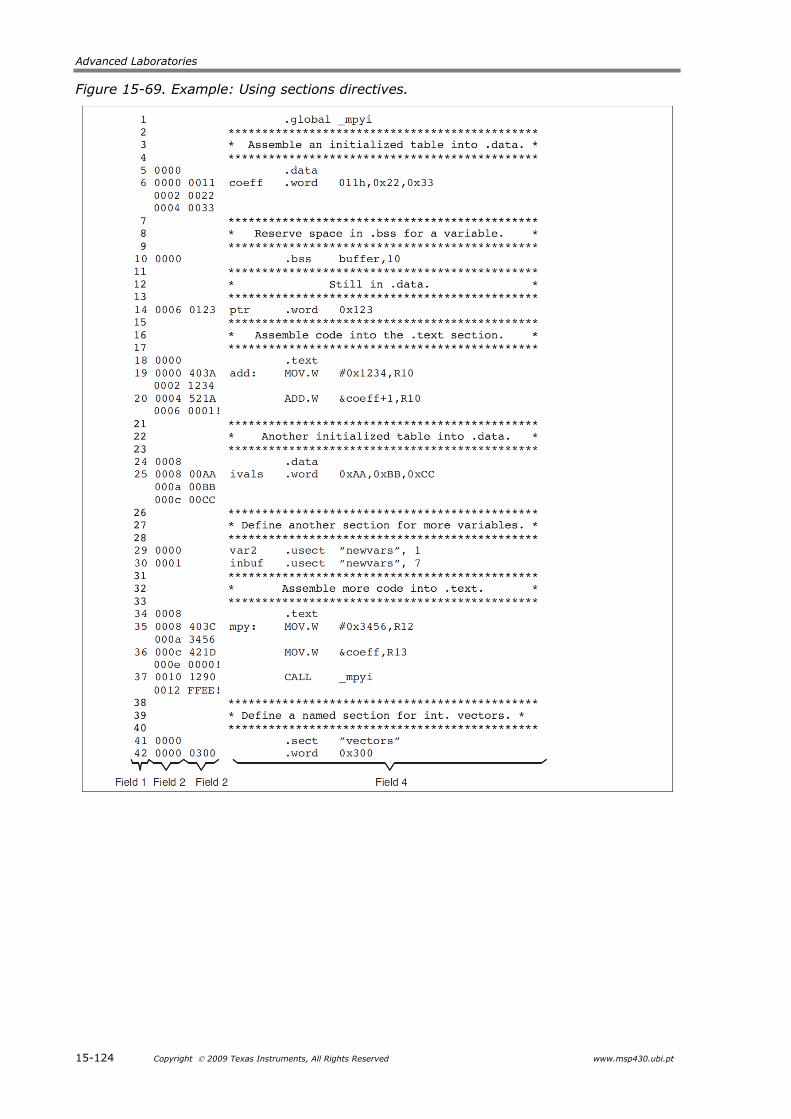
Advanced Laboratories
15-124 Copyright 2009 Texas Instruments, All Rights Reserved www.msp430.ubi.pt
Figure 15-69. Example: Using sections directives.

Lab 11c. MSP430 assembly language tutorial
www.msp430.ubi.pt Copyright 2009 Texas Instruments, All Rights Reserved 15-125
Figure 15-70 shows the process of linking two files together.
Figure 15-70. Combining input sections to form an executable object module.
Assembler directives supply data to the program and control the assembly process. Assembler directives enable you to do the following:
Assemble code and data into specified sections;
Reserve space in memory for uninitialized variables;
Control the appearance of listings;
Initialize memory;
Assemble conditional blocks;
Define global variables;
Specify libraries from which the assembler can obtain macros;
Examine symbolic debugging information.
The following tables summarize the assembler directives.

Advanced Laboratories
15-126 Copyright 2009 Texas Instruments, All Rights Reserved www.msp430.ubi.pt
Table 15-26. Directives that define sections.
Table 15-27. Directives that initialize constants (Data and Memory).
Table 15-28. Directives that perform alignment and reserve space.
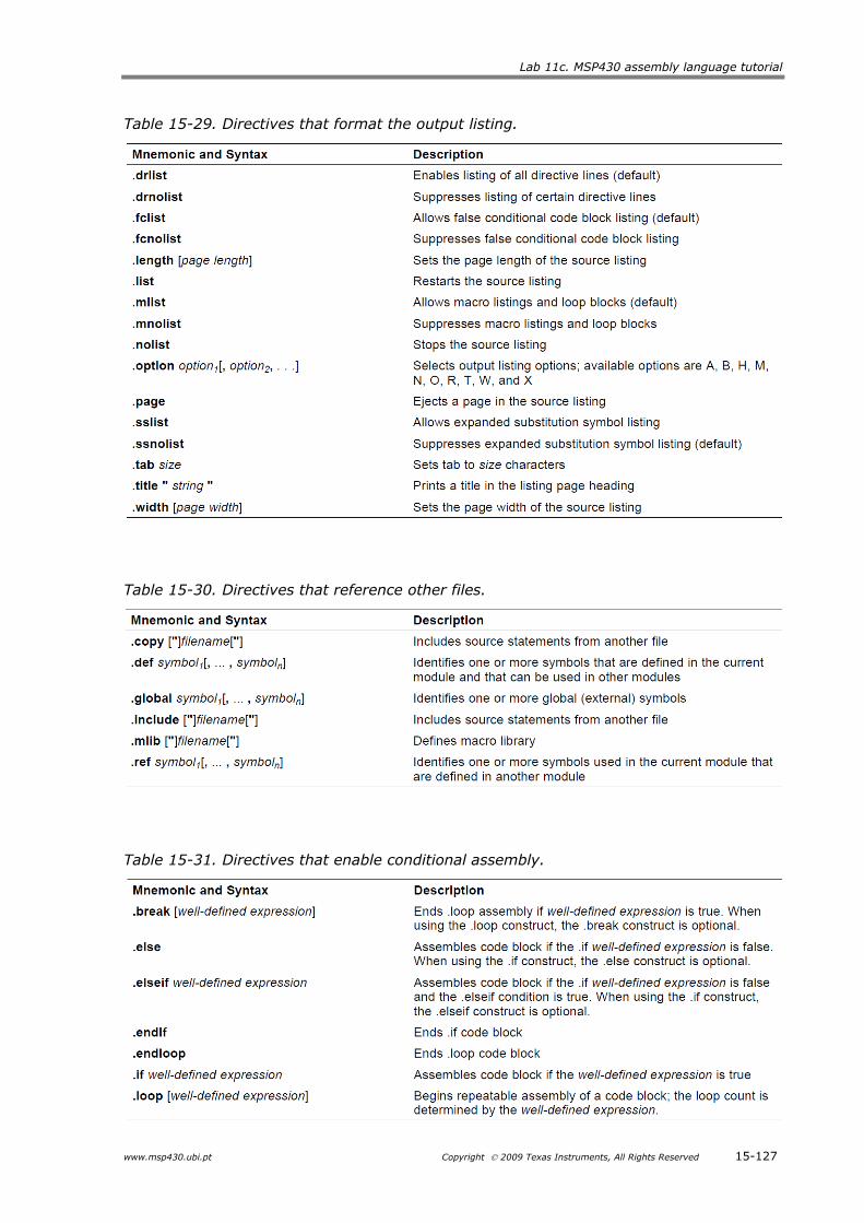
Lab 11c. MSP430 assembly language tutorial
www.msp430.ubi.pt Copyright 2009 Texas Instruments, All Rights Reserved 15-127
Table 15-29. Directives that format the output listing.
Table 15-30. Directives that reference other files.
Table 15-31. Directives that enable conditional assembly.

Advanced Laboratories
15-128 Copyright 2009 Texas Instruments, All Rights Reserved www.msp430.ubi.pt
Table 15-32. Directives that define structures.
Table 15-33. Directives that define symbols at assembly time.
Table 15-34. Directives that perform miscellaneous functions.
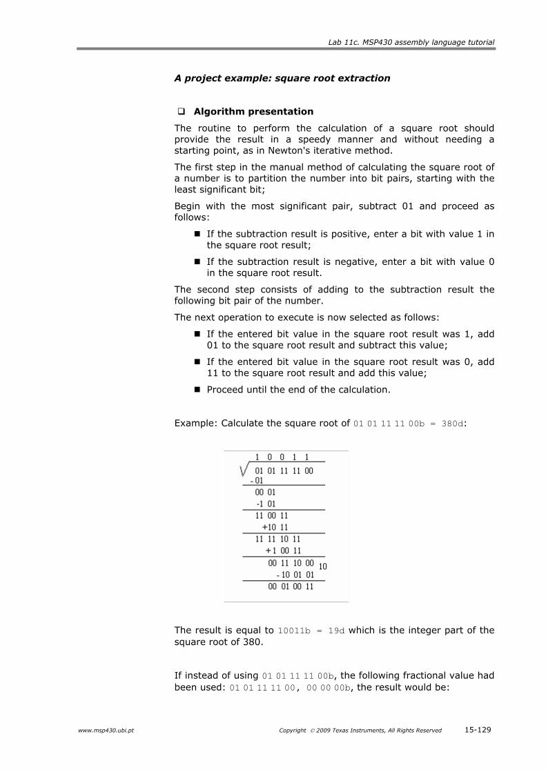
Lab 11c. MSP430 assembly language tutorial
www.msp430.ubi.pt Copyright 2009 Texas Instruments, All Rights Reserved 15-129
A project example: square root extraction
Algorithm presentation
The routine to perform the calculation of a square root should provide the result in a speedy manner and without needing a starting point, as in Newton's iterative method.
The first step in the manual method of calculating the square root of a number is to partition the number into bit pairs, starting with the least significant bit;
Begin with the most significant pair, subtract 01 and proceed as follows:
If the subtraction result is positive, enter a bit with value 1 in the square root result;
If the subtraction result is negative, enter a bit with value 0 in the square root result.
The second step consists of adding to the subtraction result the following bit pair of the number.
The next operation to execute is now selected as follows:
If the entered bit value in the square root result was 1, add 01 to the square root result and subtract this value;
If the entered bit value in the square root result was 0, add 11 to the square root result and add this value;
Proceed until the end of the calculation.
Example: Calculate the square root of 01 01 11 11 00b = 380d:
The result is equal to 10011b = 19d which is the integer part of the square root of 380.
If instead of using 01 01 11 11 00b, the following fractional value had been used: 01 01 11 11 00, 00 00 00b, the result would be:
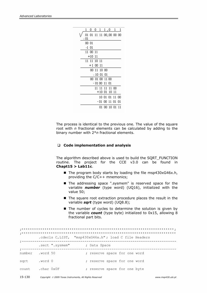
Advanced Laboratories
15-130 Copyright 2009 Texas Instruments, All Rights Reserved www.msp430.ubi.pt
The process is identical to the previous one. The value of the square root with n fractional elements can be calculated by adding to the binary number with 2*n fractional elements.
Code implementation and analysis
The algorithm described above is used to build the SQRT_FUNCTION routine. The project for the CCE v3.0 can be found in Chapt15 > Lab11c.
The program body starts by loading the file msp430xG46x.h, providing the C/C++ mnemonics;
The addressing space ".sysmem" is reserved space for the variable number (type word) (UQ16), initialized with the value 50;
The square root extraction procedure places the result in the variable sqrt (type word) (UQ8.8);
The number of cycles to determine the solution is given by the variable count (type byte) initialized to 0x15, allowing 8 fractional part bits.
;*************************************************************************; ;************************************************************************** .cdecls C,LIST, "msp430xG46x.h" ; load C file Headers ;-------------------------------------------------------------------------- .sect ".sysmem" ; Data Space ;-------------------------------------------------------------------------- number .word 50 ; reserve space for one word sqrt .word 0 ; reserve space for one word count .char 0x0F ; reserve space for one byte

Lab 11c. MSP430 assembly language tutorial
www.msp430.ubi.pt Copyright 2009 Texas Instruments, All Rights Reserved 15-131
The program code is placed in the section ".text";
After setting the entry point BEGIN, start to write the code;
The first task of the code is to initialize the stack pointer and to stop the watchdog timer;
Next comes loading the data necessary to execute the routine on the stack using the PUSH instruction;
The routine is then called. Note that it uses the CALL instruction, so the routine must reside in the address space below 64 kB. Therefore, only bits 15:0 of the register PC are placed on the stack;
After running the routine, add the value 6 to register SP (corresponding to the space occupied by the routine input data) to restore the stack pointer.
;-------------------------------------------------------------------------- .text ; Program Space ;-------------------------------------------------------------------------- .global BEGIN ; entry point BEGIN: mov.w #0A00h,SP ; initialize stackpointer mov.w #WDTPW+WDTHOLD,&WDTCTL ; stop WDT push.w #number ; push data in to stak push.w #sqrt push.w count call #SQRT_FUNCTION ; call function ADD #0x6,SP ; restore SP ret ; exit
At the beginning of the routine, the machine context is saved. Therefore, all the registers used by the routine are placed on the stack;
Also reserved on the stack is space for two temporary variables: temp1 and temp2, initialized to the values 0x00 and 0x01, respectively;
The following figure shows the stack organization:
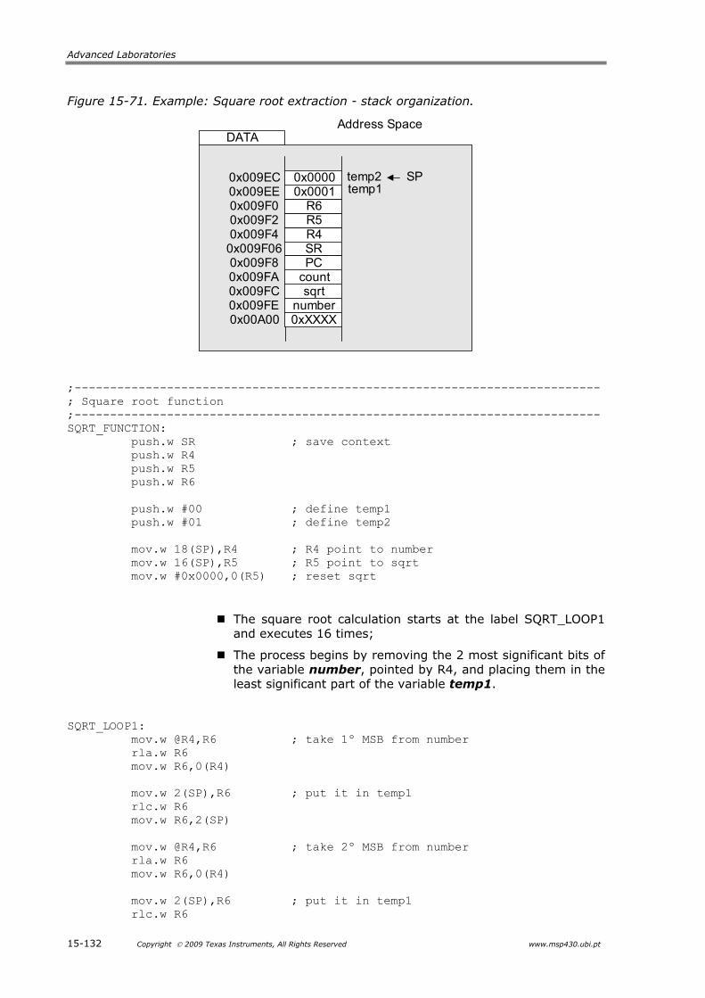
Advanced Laboratories
15-132 Copyright 2009 Texas Instruments, All Rights Reserved www.msp430.ubi.pt
Figure 15-71. Example: Square root extraction - stack organization.
Address SpaceDATA
0x0000
0xXXXX
temp2
R4R5R6
0x009EC0x0001
SR
numbersqrt
countPC
0x009EE0x009F00x009F20x009F4
0x009F060x009F80x009FA0x009FC0x009FE0x00A00
temp1SP
;-------------------------------------------------------------------------- ; Square root function ;-------------------------------------------------------------------------- SQRT_FUNCTION: push.w SR ; save context push.w R4 push.w R5 push.w R6 push.w #00 ; define temp1 push.w #01 ; define temp2 mov.w 18(SP),R4 ; R4 point to number mov.w 16(SP),R5 ; R5 point to sqrt mov.w #0x0000,0(R5) ; reset sqrt
The square root calculation starts at the label SQRT_LOOP1 and executes 16 times;
The process begins by removing the 2 most significant bits of the variable number, pointed by R4, and placing them in the least significant part of the variable temp1.
SQRT_LOOP1: mov.w @R4,R6 ; take 1º MSB from number rla.w R6 mov.w R6,0(R4) mov.w 2(SP),R6 ; put it in temp1 rlc.w R6 mov.w R6,2(SP) mov.w @R4,R6 ; take 2º MSB from number rla.w R6 mov.w R6,0(R4) mov.w 2(SP),R6 ; put it in temp1 rlc.w R6
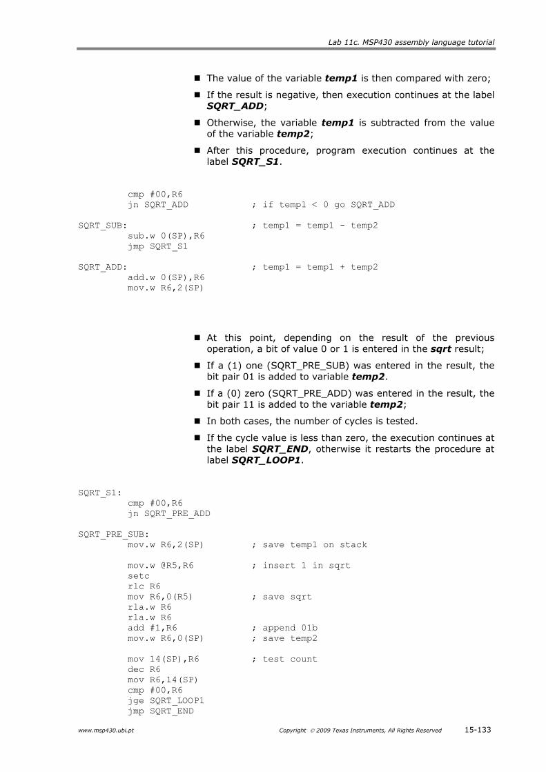
Lab 11c. MSP430 assembly language tutorial
www.msp430.ubi.pt Copyright 2009 Texas Instruments, All Rights Reserved 15-133
The value of the variable temp1 is then compared with zero;
If the result is negative, then execution continues at the label SQRT_ADD;
Otherwise, the variable temp1 is subtracted from the value of the variable temp2;
After this procedure, program execution continues at the label SQRT_S1.
cmp #00,R6 jn SQRT_ADD ; if temp1 < 0 go SQRT_ADD SQRT_SUB: ; temp1 = temp1 - temp2 sub.w 0(SP),R6 jmp SQRT_S1 SQRT_ADD: ; temp1 = temp1 + temp2 add.w 0(SP),R6 mov.w R6,2(SP)
At this point, depending on the result of the previous operation, a bit of value 0 or 1 is entered in the sqrt result;
If a (1) one (SQRT_PRE_SUB) was entered in the result, the bit pair 01 is added to variable temp2.
If a (0) zero (SQRT_PRE_ADD) was entered in the result, the bit pair 11 is added to the variable temp2;
In both cases, the number of cycles is tested.
If the cycle value is less than zero, the execution continues at the label SQRT_END, otherwise it restarts the procedure at label SQRT_LOOP1.
SQRT_S1: cmp #00,R6 jn SQRT_PRE_ADD SQRT_PRE_SUB: mov.w R6,2(SP) ; save temp1 on stack mov.w @R5,R6 ; insert 1 in sqrt setc rlc R6 mov R6,0(R5) ; save sqrt rla.w R6 rla.w R6 add #1,R6 ; append 01b mov.w R6,0(SP) ; save temp2 mov 14(SP),R6 ; test count dec R6 mov R6,14(SP) cmp #00,R6 jge SQRT_LOOP1 jmp SQRT_END

Advanced Laboratories
15-134 Copyright 2009 Texas Instruments, All Rights Reserved www.msp430.ubi.pt
SQRT_PRE_ADD: mov.w R6,2(SP) ; save temp1 on stack mov.w @R5,R6 ; insert 0 in sqrt clrc rlc R6 mov R6,0(R5) ; save sqrt rla.w R6 rla.w R6 add #3,R6 ; append 11b mov.w R6,0(SP) ; save temp2 mov 14(SP),R6 ; test count dec R6 mov R6,14(SP) cmp #00,R6 jge SQRT_LOOP1
Before ending the execution of the routine, it is necessary to restore the system state;
The data values are removed from the stack;
The execution of the routine ends with the instruction RET.
SQRT_END: pop R6 ; restore context pop R6 pop R6 pop R5 pop R4 pop SR ret ; exit
Testing the project
After the project is built and configured, it is possible to start the debugging process;
In the memory panel, enter the addresses of the variables number, sqrt and count;
Make a note of the SP value. Run the program and verify the result;
It should be noted that after using the routine, the stack returns to the same state. The square root of the value (50) is 0x712, which is the value 7.07 in the format UQ8.8.
This assembly language programming example only intends to provide an overview how a project can be created with the CCE.