16-mbit, page-erasable serial flash memory with byte ... · 2.1 serial data output (q) ... 6.3 read...
TRANSCRIPT
April 2008 Rev 6 1/58
1
M25PE1616-Mbit, page-erasable serial flash memory with
byte-alterability, 75 MHz SPI bus, standard pinout
Features SPI bus compatible serial interface
16-Mbit page-erasable Flash memory
Page size: 256 bytes– Page write in 11 ms (typical)– Page program in 0.8 ms (typical)– Page erase in 10 ms (typical)
Subsector erase (4 Kbytes)
Sector erase (64 Kbytes)
Bulk erase (16 Mbits)
2.7 V to 3.6 V single supply voltage
75 MHz clock rate (maximum)
Deep power-down mode 1 µA (typical)
Electronic signature– JEDEC standard two-byte signature
(8015h)– Unique ID code (UID) with 16 bytes read-
only, available upon customer request
Software write protection on a 64-Kbyte sector basis
Hardware write protection of the memory area selected using the BP0, BP1 and BP2 bits
More than 100 000 write cycles
More than 20 years data retention
Packages– ECOPACK® (RoHS compliant)
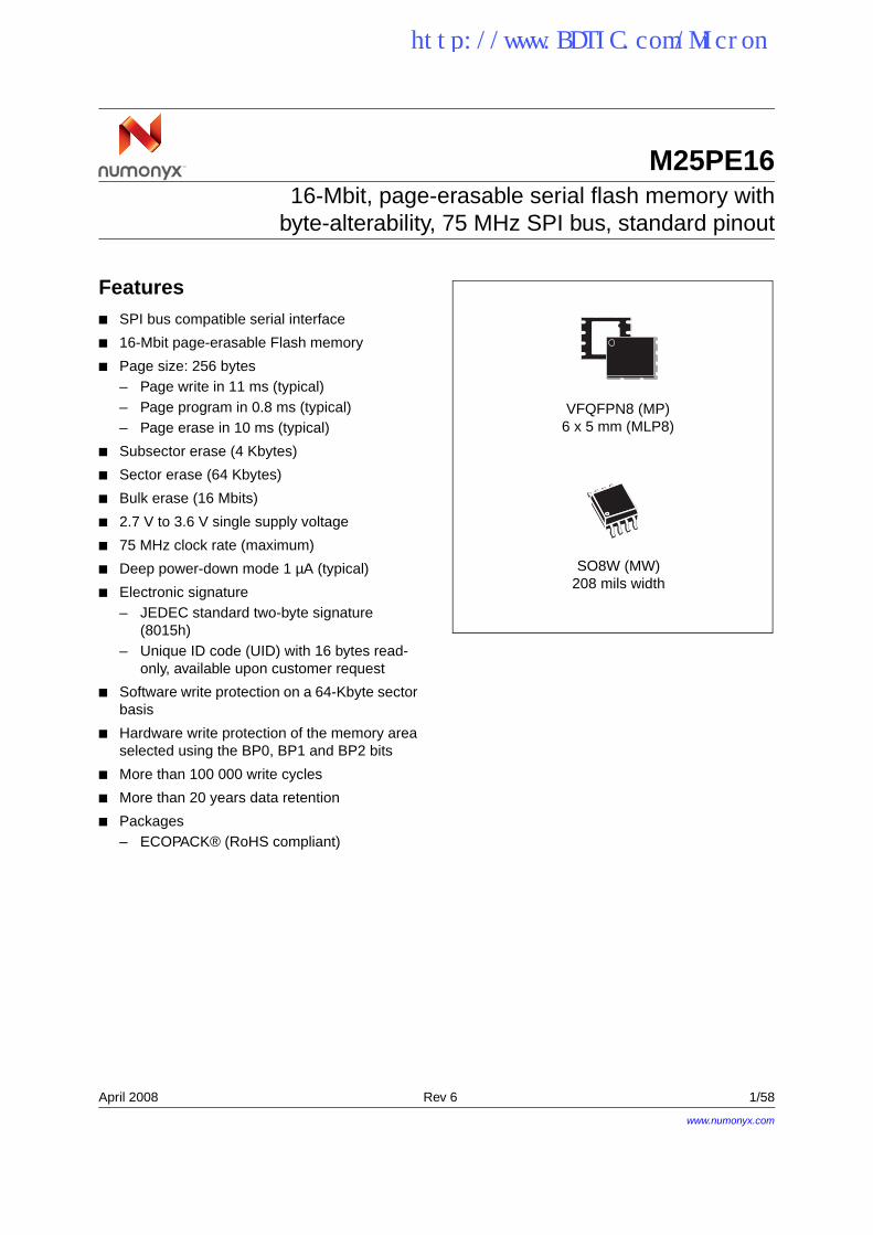
VFQFPN8 (MP)6 x 5 mm (MLP8)
SO8W (MW)208 mils width
www.numonyx.com
http://www.BDTIC.com/Micron
Contents M25PE16
2/58
Contents
1 Description . . . . . . . . . . . . . . . . . . . . . . . . . . . . . . . . . . . . . . . . . . . . . . . . . 6
2 Signal descriptions . . . . . . . . . . . . . . . . . . . . . . . . . . . . . . . . . . . . . . . . . . 8
2.1 Serial data output (Q) . . . . . . . . . . . . . . . . . . . . . . . . . . . . . . . . . . . . . . . . . 8
2.2 Serial data input (D) . . . . . . . . . . . . . . . . . . . . . . . . . . . . . . . . . . . . . . . . . . 8
2.3 Serial clock (C) . . . . . . . . . . . . . . . . . . . . . . . . . . . . . . . . . . . . . . . . . . . . . . 8
2.4 Chip select (S) . . . . . . . . . . . . . . . . . . . . . . . . . . . . . . . . . . . . . . . . . . . . . . 8
2.5 Reset (Reset) . . . . . . . . . . . . . . . . . . . . . . . . . . . . . . . . . . . . . . . . . . . . . . . 8
2.6 Write protect (W) . . . . . . . . . . . . . . . . . . . . . . . . . . . . . . . . . . . . . . . . . . . . 8
2.7 VCC supply voltage . . . . . . . . . . . . . . . . . . . . . . . . . . . . . . . . . . . . . . . . . . . 9
2.8 VSS ground . . . . . . . . . . . . . . . . . . . . . . . . . . . . . . . . . . . . . . . . . . . . . . . . . 9
3 SPI modes . . . . . . . . . . . . . . . . . . . . . . . . . . . . . . . . . . . . . . . . . . . . . . . . 10
4 Operating features . . . . . . . . . . . . . . . . . . . . . . . . . . . . . . . . . . . . . . . . . 12
4.1 Sharing the overhead of modifying data . . . . . . . . . . . . . . . . . . . . . . . . . . 12
4.2 An easy way to modify data . . . . . . . . . . . . . . . . . . . . . . . . . . . . . . . . . . . 12
4.3 A fast way to modify data . . . . . . . . . . . . . . . . . . . . . . . . . . . . . . . . . . . . . 13
4.4 Polling during a write, program or erase cycle . . . . . . . . . . . . . . . . . . . . . 13
4.5 Reset . . . . . . . . . . . . . . . . . . . . . . . . . . . . . . . . . . . . . . . . . . . . . . . . . . . . 13
4.6 Active power, standby power and deep power-down modes . . . . . . . . . . 13
4.7 Status register . . . . . . . . . . . . . . . . . . . . . . . . . . . . . . . . . . . . . . . . . . . . . 14
4.8 Protection modes . . . . . . . . . . . . . . . . . . . . . . . . . . . . . . . . . . . . . . . . . . . 14
4.8.1 Protocol-related protections . . . . . . . . . . . . . . . . . . . . . . . . . . . . . . . . . . 14
4.8.2 Specific hardware and software protections . . . . . . . . . . . . . . . . . . . . . 15
5 Memory organization . . . . . . . . . . . . . . . . . . . . . . . . . . . . . . . . . . . . . . . 17
6 Instructions . . . . . . . . . . . . . . . . . . . . . . . . . . . . . . . . . . . . . . . . . . . . . . . 20
6.1 Write enable (WREN) . . . . . . . . . . . . . . . . . . . . . . . . . . . . . . . . . . . . . . . . 22
6.2 Write disable (WRDI) . . . . . . . . . . . . . . . . . . . . . . . . . . . . . . . . . . . . . . . . 23
6.3 Read identification (RDID) . . . . . . . . . . . . . . . . . . . . . . . . . . . . . . . . . . . . 24
http://www.BDTIC.com/Micron
M25PE16 Contents
3/58
6.4 Read status register (RDSR) . . . . . . . . . . . . . . . . . . . . . . . . . . . . . . . . . . 25
6.4.1 WIP bit . . . . . . . . . . . . . . . . . . . . . . . . . . . . . . . . . . . . . . . . . . . . . . . . . . 25
6.4.2 WEL bit . . . . . . . . . . . . . . . . . . . . . . . . . . . . . . . . . . . . . . . . . . . . . . . . . 25
6.4.3 BP2, BP1, BP0 bits . . . . . . . . . . . . . . . . . . . . . . . . . . . . . . . . . . . . . . . . 25
6.4.4 SRWD bit . . . . . . . . . . . . . . . . . . . . . . . . . . . . . . . . . . . . . . . . . . . . . . . . 25
6.5 Write status register (WRSR) . . . . . . . . . . . . . . . . . . . . . . . . . . . . . . . . . . 27
6.6 Read data bytes (READ) . . . . . . . . . . . . . . . . . . . . . . . . . . . . . . . . . . . . . 29
6.7 Read data bytes at higher speed (FAST_READ) . . . . . . . . . . . . . . . . . . . 30
6.8 Read lock register (RDLR) . . . . . . . . . . . . . . . . . . . . . . . . . . . . . . . . . . . . 31
6.9 Page write (PW) . . . . . . . . . . . . . . . . . . . . . . . . . . . . . . . . . . . . . . . . . . . . 32
6.10 Page program (PP) . . . . . . . . . . . . . . . . . . . . . . . . . . . . . . . . . . . . . . . . . . 34
6.11 Write to lock register (WRLR) . . . . . . . . . . . . . . . . . . . . . . . . . . . . . . . . . . 36
6.12 Page erase (PE) . . . . . . . . . . . . . . . . . . . . . . . . . . . . . . . . . . . . . . . . . . . . 37
6.13 Sector erase (SE) . . . . . . . . . . . . . . . . . . . . . . . . . . . . . . . . . . . . . . . . . . . 38
6.14 Subsector erase (SSE) . . . . . . . . . . . . . . . . . . . . . . . . . . . . . . . . . . . . . . . 39
6.15 Bulk erase (BE) . . . . . . . . . . . . . . . . . . . . . . . . . . . . . . . . . . . . . . . . . . . . 40
6.16 Deep power-down (DP) . . . . . . . . . . . . . . . . . . . . . . . . . . . . . . . . . . . . . . 41
6.17 Release from deep power-down (RDP) . . . . . . . . . . . . . . . . . . . . . . . . . . 42
7 Power-up and power-down . . . . . . . . . . . . . . . . . . . . . . . . . . . . . . . . . . . 43
8 Reset . . . . . . . . . . . . . . . . . . . . . . . . . . . . . . . . . . . . . . . . . . . . . . . . . . . . . 45
9 Initial delivery state . . . . . . . . . . . . . . . . . . . . . . . . . . . . . . . . . . . . . . . . . 45
10 Maximum ratings . . . . . . . . . . . . . . . . . . . . . . . . . . . . . . . . . . . . . . . . . . . 46
11 DC and AC parameters . . . . . . . . . . . . . . . . . . . . . . . . . . . . . . . . . . . . . . 47
12 Package mechanical . . . . . . . . . . . . . . . . . . . . . . . . . . . . . . . . . . . . . . . . 53
13 Ordering information . . . . . . . . . . . . . . . . . . . . . . . . . . . . . . . . . . . . . . . 56
14 Revision history . . . . . . . . . . . . . . . . . . . . . . . . . . . . . . . . . . . . . . . . . . . 57
http://www.BDTIC.com/Micron
List of tables M25PE16
4/58
List of tables
Table 1. Signal names . . . . . . . . . . . . . . . . . . . . . . . . . . . . . . . . . . . . . . . . . . . . . . . . . . . . . . . . . . . . 7Table 2. Software protection truth table (sectors 0 to 31, 64-Kbyte granularity). . . . . . . . . . . . . . . . 15Table 3. Protected area sizes . . . . . . . . . . . . . . . . . . . . . . . . . . . . . . . . . . . . . . . . . . . . . . . . . . . . . . 16Table 4. Memory organization . . . . . . . . . . . . . . . . . . . . . . . . . . . . . . . . . . . . . . . . . . . . . . . . . . . . . 17Table 5. Instruction set . . . . . . . . . . . . . . . . . . . . . . . . . . . . . . . . . . . . . . . . . . . . . . . . . . . . . . . . . . . 21Table 6. Read identification (RDID) data-out sequence . . . . . . . . . . . . . . . . . . . . . . . . . . . . . . . . . . 24Table 7. Status register format . . . . . . . . . . . . . . . . . . . . . . . . . . . . . . . . . . . . . . . . . . . . . . . . . . . . 25Table 8. Protection modes . . . . . . . . . . . . . . . . . . . . . . . . . . . . . . . . . . . . . . . . . . . . . . . . . . . . . . . . 28Table 9. Lock register out . . . . . . . . . . . . . . . . . . . . . . . . . . . . . . . . . . . . . . . . . . . . . . . . . . . . . . . . . 31Table 10. Lock register in . . . . . . . . . . . . . . . . . . . . . . . . . . . . . . . . . . . . . . . . . . . . . . . . . . . . . . . . . . 36Table 11. Power-up timing and VWI threshold . . . . . . . . . . . . . . . . . . . . . . . . . . . . . . . . . . . . . . . . . . 44Table 12. Device status after a Reset Low pulse . . . . . . . . . . . . . . . . . . . . . . . . . . . . . . . . . . . . . . . . 45Table 13. Absolute maximum ratings . . . . . . . . . . . . . . . . . . . . . . . . . . . . . . . . . . . . . . . . . . . . . . . . . 46Table 14. Operating conditions. . . . . . . . . . . . . . . . . . . . . . . . . . . . . . . . . . . . . . . . . . . . . . . . . . . . . . 47Table 15. AC measurement conditions. . . . . . . . . . . . . . . . . . . . . . . . . . . . . . . . . . . . . . . . . . . . . . . . 47Table 16. Capacitance . . . . . . . . . . . . . . . . . . . . . . . . . . . . . . . . . . . . . . . . . . . . . . . . . . . . . . . . . . . . 47Table 17. DC characteristics. . . . . . . . . . . . . . . . . . . . . . . . . . . . . . . . . . . . . . . . . . . . . . . . . . . . . . . . 48Table 18. AC characteristics (50 MHz operation) . . . . . . . . . . . . . . . . . . . . . . . . . . . . . . . . . . . . . . . . 49Table 19. AC characteristics (75 MHz operation) . . . . . . . . . . . . . . . . . . . . . . . . . . . . . . . . . . . . . . . . 50Table 20. Reset conditions . . . . . . . . . . . . . . . . . . . . . . . . . . . . . . . . . . . . . . . . . . . . . . . . . . . . . . . . . 52Table 21. Timings after a Reset Low pulse . . . . . . . . . . . . . . . . . . . . . . . . . . . . . . . . . . . . . . . . . . . . 52Table 22. VFQFPN8 (MLP8) 8-lead very thin fine pitch quad flat package no lead,
6 × 5 mm, package mechanical data . . . . . . . . . . . . . . . . . . . . . . . . . . . . . . . . . . . . . . . . . 54Table 23. SO8 wide – 8 lead plastic small outline, 208 mils body width, mechanical data. . . . . . . . . 55Table 24. Ordering information scheme . . . . . . . . . . . . . . . . . . . . . . . . . . . . . . . . . . . . . . . . . . . . . . . 56Table 25. Document revision history . . . . . . . . . . . . . . . . . . . . . . . . . . . . . . . . . . . . . . . . . . . . . . . . . 57
http://www.BDTIC.com/Micron
M25PE16 List of figures
5/58
List of figures
Figure 1. Logic diagram . . . . . . . . . . . . . . . . . . . . . . . . . . . . . . . . . . . . . . . . . . . . . . . . . . . . . . . . . . . . 7Figure 2. VFQFPN and SO connections . . . . . . . . . . . . . . . . . . . . . . . . . . . . . . . . . . . . . . . . . . . . . . . 7Figure 3. Bus master and memory devices on the SPI bus. . . . . . . . . . . . . . . . . . . . . . . . . . . . . . . . 10Figure 4. SPI modes supported . . . . . . . . . . . . . . . . . . . . . . . . . . . . . . . . . . . . . . . . . . . . . . . . . . . . . 11Figure 5. Block diagram . . . . . . . . . . . . . . . . . . . . . . . . . . . . . . . . . . . . . . . . . . . . . . . . . . . . . . . . . . . 19Figure 6. Write enable (WREN) instruction sequence . . . . . . . . . . . . . . . . . . . . . . . . . . . . . . . . . . . . 22Figure 7. Write disable (WRDI) instruction sequence . . . . . . . . . . . . . . . . . . . . . . . . . . . . . . . . . . . . 23Figure 8. Read identification (RDID) instruction sequence and data-out sequence . . . . . . . . . . . . . 24Figure 9. Read status register (RDSR) instruction sequence and data-out sequence . . . . . . . . . . . 26Figure 10. Write status register (WRSR) instruction sequence . . . . . . . . . . . . . . . . . . . . . . . . . . . . . . 27Figure 11. Read data bytes (READ) instruction sequence and data-out sequence . . . . . . . . . . . . . . 29Figure 12. Read data bytes at higher speed (FAST_READ) instruction sequence
and data-out sequence . . . . . . . . . . . . . . . . . . . . . . . . . . . . . . . . . . . . . . . . . . . . . . . . . . . . 30Figure 13. Read lock register (RDLR) instruction sequence
and data-out sequence . . . . . . . . . . . . . . . . . . . . . . . . . . . . . . . . . . . . . . . . . . . . . . . . . . . . 31Figure 14. Page write (PW) instruction sequence . . . . . . . . . . . . . . . . . . . . . . . . . . . . . . . . . . . . . . . . 33Figure 15. Page program (PP) instruction sequence. . . . . . . . . . . . . . . . . . . . . . . . . . . . . . . . . . . . . . 35Figure 16. Write to lock register (WRLR) instruction sequence . . . . . . . . . . . . . . . . . . . . . . . . . . . . . . 36Figure 17. Page erase (PE) instruction sequence . . . . . . . . . . . . . . . . . . . . . . . . . . . . . . . . . . . . . . . . 37Figure 18. Sector erase (SE) instruction sequence . . . . . . . . . . . . . . . . . . . . . . . . . . . . . . . . . . . . . . . 38Figure 19. Subsector erase (SSE) instruction sequence . . . . . . . . . . . . . . . . . . . . . . . . . . . . . . . . . . . 39Figure 20. Bulk erase (BE) instruction sequence. . . . . . . . . . . . . . . . . . . . . . . . . . . . . . . . . . . . . . . . . 40Figure 21. Deep power-down (DP) instruction sequence . . . . . . . . . . . . . . . . . . . . . . . . . . . . . . . . . . 41Figure 22. Release from deep power-down (RDP) instruction sequence . . . . . . . . . . . . . . . . . . . . . . 42Figure 23. Power-up timing . . . . . . . . . . . . . . . . . . . . . . . . . . . . . . . . . . . . . . . . . . . . . . . . . . . . . . . . . 44Figure 24. AC measurement I/O waveform . . . . . . . . . . . . . . . . . . . . . . . . . . . . . . . . . . . . . . . . . . . . . 47Figure 25. Serial input timing . . . . . . . . . . . . . . . . . . . . . . . . . . . . . . . . . . . . . . . . . . . . . . . . . . . . . . . . 51Figure 26. Write protect setup and hold timing . . . . . . . . . . . . . . . . . . . . . . . . . . . . . . . . . . . . . . . . . . 51Figure 27. Output timing . . . . . . . . . . . . . . . . . . . . . . . . . . . . . . . . . . . . . . . . . . . . . . . . . . . . . . . . . . . 51Figure 28. Reset AC waveforms while a program or erase cycle is in progress . . . . . . . . . . . . . . . . . 52Figure 29. VFQFPN8 (MLP8) 8-lead very thin dual flat package no lead, 6 × 5 mm,
package outline. . . . . . . . . . . . . . . . . . . . . . . . . . . . . . . . . . . . . . . . . . . . . . . . . . . . . . . . . . 53Figure 30. SO8 wide – 8 lead plastic small outline, 208 mils body width, package outline . . . . . . . . . 55
http://www.BDTIC.com/Micron
Description M25PE16
6/58
1 Description
The M25PE16 is a 16-Mbit (2 Mbits × 8) serial paged flash memory accessed by a high speed SPI-compatible bus.
The memory can be written or programmed 1 to 256 bytes at a time, using the page write or page program instruction. The page write instruction consists of an integrated page erase cycle followed by a page program cycle.
The memory is organized as 32 sectors that are further divided up into 16 subsectors each (512 subsectors in total). Each sector contains 256 pages and each subsector contains 16 pages. Each page is 256-byte wide. Thus, the whole memory can be viewed as consisting of 8192 pages, or 2,097,152 bytes.
The memory can be erased a page at a time, using the page erase instruction, a subsector at a time, using the subsector erase instruction, a sector at a time, using the sector erase instruction, or as a whole, using the bulk erase instruction.
The memory can be write protected by either hardware or software using mixed volatile and non-volatile protection features, depending on the application needs. The protection granularity is of 64 Kbytes (sector granularity).
http://www.BDTIC.com/Micron
M25PE16 Description
7/58
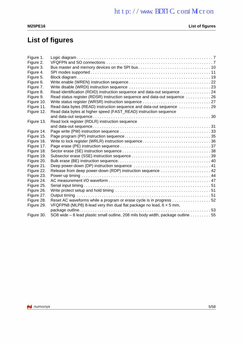
Figure 1. Logic diagram
Figure 2. VFQFPN and SO connections
1. There is an exposed die paddle on the underside of the MLP8 package. This is pulled, internally, to VSS, and must not be allowed to be connected to any other voltage or signal line on the PCB.
2. See Section 12: Package mechanical for package dimensions, and how to identify pin-1.
Table 1. Signal names
Signal name Function Direction
C Serial clock Input
D Serial data input Input
Q Serial data output Output
S Chip select Input
W Write protect Input
Reset Reset Input
VCC Supply voltage –
VSS Ground –
Reset
AI12343c
S
VCC
M25PE16
VSS
Q
C
D
W
1
AI12344c
234
8765 DVSS
CResetQ
S VCC
M25PE16
W
http://www.BDTIC.com/Micron
Signal descriptions M25PE16
8/58
2 Signal descriptions
2.1 Serial data output (Q)This output signal is used to transfer data serially out of the device. Data is shifted out on the falling edge of Serial Clock (C).
2.2 Serial data input (D)This input signal is used to transfer data serially into the device. It receives instructions, addresses, and the data to be programmed. Values are latched on the rising edge of Serial Clock (C).
2.3 Serial clock (C)This input signal provides the timing of the serial interface. Instructions, addresses, or data present at Serial Data Input (D) are latched on the rising edge of Serial Clock (C). Data on Serial Data Output (Q) changes after the falling edge of Serial Clock (C).
2.4 Chip select (S)When this input signal is High, the device is deselected and serial data output (Q) is at high impedance. Unless an internal read, program, erase or write cycle is in progress, the device will be in the standby mode (this is not the deep power-down mode). Driving Chip Select (S) Low selects the device, placing it in the active power mode.
After power-up, a falling edge on Chip Select (S) is required prior to the start of any instruction.
2.5 Reset (Reset)The Reset (Reset) input provides a hardware reset for the memory.
When Reset (Reset) is driven High, the memory is in the normal operating mode. When Reset (Reset) is driven Low, the memory will enter the reset mode. In this mode, the output is high impedance.
Driving Reset (Reset) Low while an internal operation is in progress will affect this operation (write, program or erase cycle) and data may be lost.
See Table 12 for the status of the device after a Reset Low pulse.
2.6 Write protect (W)The write protect (W) input is used to freeze the size of the area of memory that is protected against write, program and erase instructions (as specified by the values in the BP2, BP1 and BP0 bits of the status register). See Section 6.4: Read status register (RDSR).
http://www.BDTIC.com/Micron
M25PE16 Signal descriptions
9/58
2.7 VCC supply voltageVCC is the supply voltage.
2.8 VSS groundVSS is the reference for the VCC supply voltage.
http://www.BDTIC.com/Micron
SPI modes M25PE16
10/58
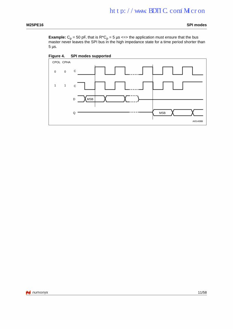
3 SPI modes
These devices can be driven by a microcontroller with its SPI peripheral running in either of the two following modes:
CPOL=0, CPHA=0
CPOL=1, CPHA=1
For these two modes, input data is latched in on the rising edge of Serial Clock (C), and output data is available from the falling edge of Serial Clock (C).
The difference between the two modes, as shown in Figure 4, is the clock polarity when the bus master is in Stand-by mode and not transferring data:
C remains at 0 for (CPOL=0, CPHA=0)
C remains at 1 for (CPOL=1, CPHA=1)
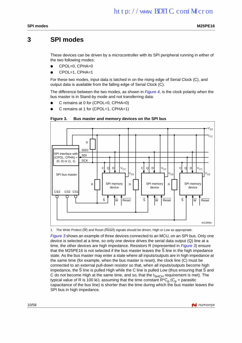
Figure 3. Bus master and memory devices on the SPI bus
1. The Write Protect (W) and Reset (Reset) signals should be driven, High or Low as appropriate.
Figure 3 shows an example of three devices connected to an MCU, on an SPI bus. Only one device is selected at a time, so only one device drives the serial data output (Q) line at a time, the other devices are high impedance. Resistors R (represented in Figure 3) ensure that the M25PE16 is not selected if the bus master leaves the S line in the high impedance state. As the bus master may enter a state where all inputs/outputs are in high impedance at the same time (for example, when the bus master is reset), the clock line (C) must be connected to an external pull-down resistor so that, when all inputs/outputs become high impedance, the S line is pulled High while the C line is pulled Low (thus ensuring that S and C do not become High at the same time, and so, that the tSHCH requirement is met). The typical value of R is 100 kΩ, assuming that the time constant R*Cp (Cp = parasitic capacitance of the bus line) is shorter than the time during which the bus master leaves the SPI bus in high impedance.
AI12836c
SPI bus master
SPI memorydevice
SDO
SDI
SCK
C Q D
S
SPI memorydevice
C Q D
S
SPI memorydevice
C Q D
S
CS3 CS2 CS1
SPI interface with(CPOL, CPHA) =
(0, 0) or (1, 1)
W Reset W Reset W Reset
R R R
VCC
VCC VCC VCC
VSS
VSS VSS VSS
R
http://www.BDTIC.com/Micron
M25PE16 SPI modes
11/58
Example: Cp = 50 pF, that is R*Cp = 5 µs <=> the application must ensure that the bus master never leaves the SPI bus in the high impedance state for a time period shorter than 5 µs.
Figure 4. SPI modes supported
AI01438B
C
MSB
CPHA
D
0
1
CPOL
0
1
Q
C
MSB
http://www.BDTIC.com/Micron
Operating features M25PE16
12/58
4 Operating features
4.1 Sharing the overhead of modifying dataTo write or program one (or more) data bytes, two instructions are required: write enable (WREN), which is one byte, and a page write (PW) or page program (PP) sequence, which consists of four bytes plus data. This is followed by the internal cycle (of duration tPW or tPP).
To share this overhead, the page write (PW) or page program (PP) instruction allows up to 256 bytes to be programmed (changing bits from ‘1’ to ‘0’) or written (changing bits to ‘0’ or ‘1’) at a time, provided that they lie in consecutive addresses on the same page of memory.
4.2 An easy way to modify dataThe page write (PW) instruction provides a convenient way of modifying data (up to 256 contiguous bytes at a time), and simply requires the start address, and the new data in the instruction sequence.
The page write (PW) instruction is entered by driving Chip Select (S) Low, and then transmitting the instruction byte, three address bytes (A23-A0) and at least one data byte, and then driving Chip Select (S) High. While Chip Select (S) is being held Low, the data bytes are written to the data buffer, starting at the address given in the third address byte (A7-A0). When Chip Select (S) is driven High, the write cycle starts. The remaining, unchanged, bytes of the data buffer are automatically loaded with the values of the corresponding bytes of the addressed memory page. The addressed memory page then automatically put into an erase cycle. Finally, the addressed memory page is programmed with the contents of the data buffer.
All of this buffer management is handled internally, and is transparent to the user. The user is given the facility of being able to alter the contents of the memory on a byte-by-byte basis.
For optimized timings, it is recommended to use the page write (PW) instruction to write all consecutive targeted bytes in a single sequence versus using several page write (PW) sequences with each containing only a few bytes (see Section 6.9: Page write (PW), Table 18: AC characteristics (50 MHz operation), and Table 19: AC characteristics (75 MHz operation)).
http://www.BDTIC.com/Micron
M25PE16 Operating features
13/58
4.3 A fast way to modify dataThe page program (PP) instruction provides a fast way of modifying data (up to 256 contiguous bytes at a time), provided that it only involves resetting bits to ‘0’ that had previously been set to ‘1’.
This might be:
when the designer is programming the device for the first time
when the designer knows that the page has already been erased by an earlier page erase (PE), subsector erase (SSE), sector erase (SE) or bulk erase (BE) instruction. This is useful, for example, when storing a fast stream of data, having first performed the erase cycle when time was available
when the designer knows that the only changes involve resetting bits to 0 that are still set to ‘1’. When this method is possible, it has the additional advantage of minimizing the number of unnecessary erase operations, and the extra stress incurred by each page.
For optimized timings, it is recommended to use the page program (PP) instruction to program all consecutive targeted bytes in a single sequence versus using several page program (PP) sequences with each containing only a few bytes (see Section 6.10: Page program (PP), Table 18: AC characteristics (50 MHz operation), and Table 19: AC characteristics (75 MHz operation)).
4.4 Polling during a write, program or erase cycleA further improvement in the time to write (PW, WRSR), program (PP) or erase (SE, SSE or BE) can be achieved by not waiting for the worst case delay (tW, tPW, tPP, tPE, tSE, tSSE or tBE). The write in progress (WIP) bit is provided in the status register so that the application program can monitor its value, polling it to establish when the previous cycle is complete.
4.5 ResetAn internal power-on reset circuit helps protect against inadvertent data writes. Addition protection is provided by driving Reset (Reset) Low during the power-on process, and only driving it High when VCC has reached the correct voltage level, VCC(min).
4.6 Active power, standby power and deep power-down modesWhen Chip Select (S) is Low, the device is selected, and in the active power mode.
When Chip Select (S) is High, the device is deselected, but could remain in the active power mode until all internal cycles have completed (program, erase, write). The device then goes in to the standby power mode. The device consumption drops to ICC1.
The deep power-down mode is entered when the specific instruction (the deep power-down (DP) instruction) is executed. The device consumption drops further to ICC2. When in this mode, only the release from deep power-down instruction is accepted. All other instructions are ignored. The device remains in the deep power-down mode until the release from deep power-down instruction is executed. This can be used as an extra software protection mechanism, when the device is not in active use, to protect the device from inadvertent write, program or erase instructions.
http://www.BDTIC.com/Micron
Operating features M25PE16
14/58
4.7 Status registerThe status register contains a number of status and control bits that can be read or set (as appropriate) by using specific instructions. See Section 6.4: Read status register (RDSR) for a detailed description of the status register bits.
4.8 Protection modesThe environments where non-volatile memory devices are used can be very noisy. No SPI device can operate correctly in the presence of excessive noise. To help combat this and to meet the needs of modularized applications, the M25PE16 features the following flexible data protection mechanisms:
4.8.1 Protocol-related protections
Power on reset and an internal timer (tPUW) can provide protection against inadvertent changes while the power supply is outside the operating specification.
Program, erase and write instructions are checked that they consist of a number of clock pulses that is a multiple of eight, before they are accepted for execution.
All instructions that modify data must be preceded by a write enable (WREN) instruction to set the write enable latch (WEL) bit. This bit is returned to its reset state by the following events:
– Power-up
– Reset (Reset) driven Low
– Write disable (WRDI) instruction completion
– Page write (PW) instruction completion
– Write status register (WRSR) instruction completion
– Page program (PP) instruction completion
– Write to lock register (WRLR) instruction completion
– Page erase (PE) instruction completion
– Subsector erase (SSE) instruction completion
– Sector erase (SE) instruction completion
– Bulk erase (BE) instruction completion
The Reset (Reset) signal can be driven Low to freeze and reset the internal logic. For the specific cases of program and write cycles, the designer should refer to Section 6.5: Write status register (WRSR), Section 6.9: Page write (PW), Section 6.10: Page program (PP), Section 6.12: Page erase (PE), Section 6.13: Sector erase (SE) and Section 6.14: Subsector erase (SSE), and to Table 12: Device status after a Reset Low pulse.
In addition to the low power consumption feature, the deep power-down mode offers extra software protection from inadvertent write, program and erase instructions while the device is not in active use.
http://www.BDTIC.com/Micron
M25PE16 Operating features
15/58
4.8.2 Specific hardware and software protections
There are two software protected modes, SPM1 and SPM2, that can be combined to protect the memory array as required. The SPM2 can be hardware protected with the help of the W input pin.
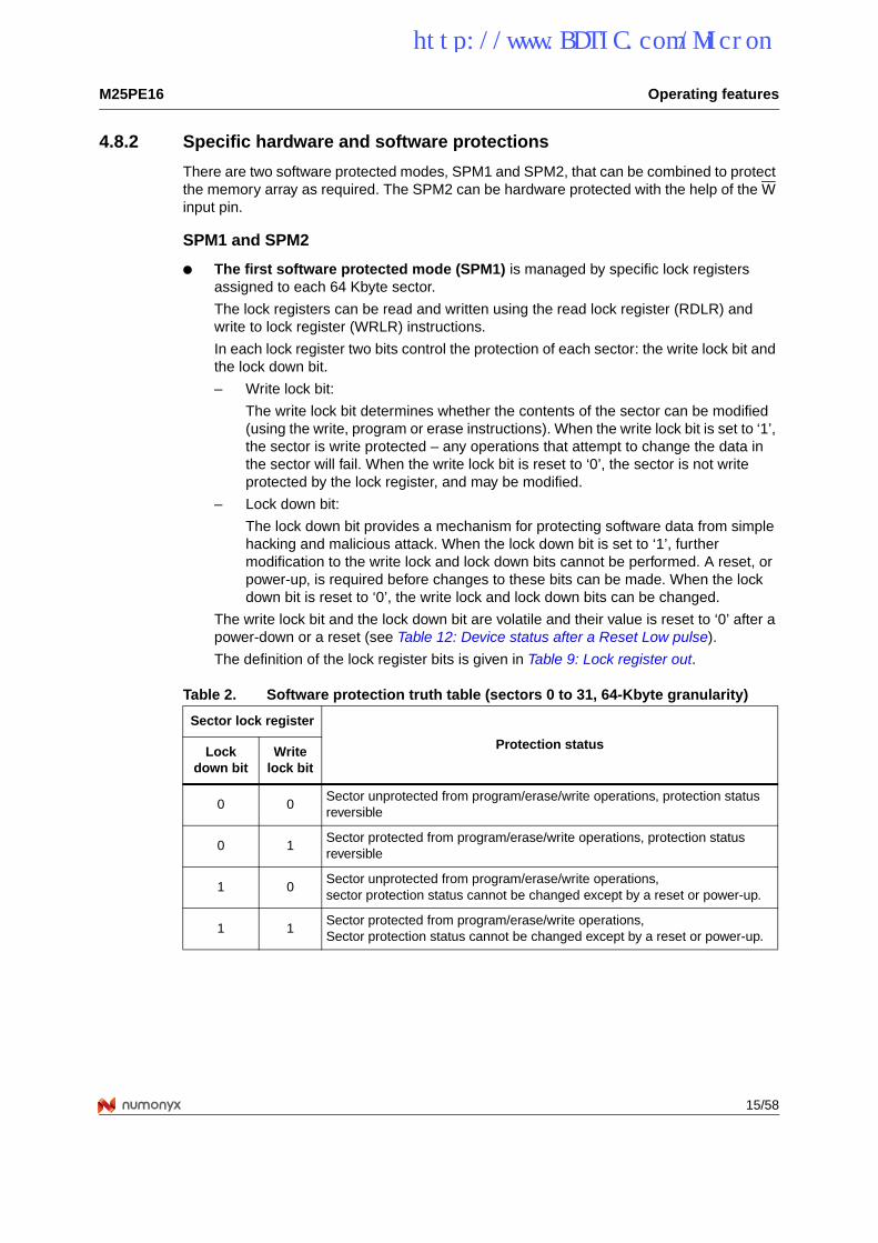
SPM1 and SPM2
The first software protected mode (SPM1) is managed by specific lock registers assigned to each 64 Kbyte sector.
The lock registers can be read and written using the read lock register (RDLR) and write to lock register (WRLR) instructions.
In each lock register two bits control the protection of each sector: the write lock bit and the lock down bit.
– Write lock bit:
The write lock bit determines whether the contents of the sector can be modified (using the write, program or erase instructions). When the write lock bit is set to ‘1’, the sector is write protected – any operations that attempt to change the data in the sector will fail. When the write lock bit is reset to ‘0’, the sector is not write protected by the lock register, and may be modified.
– Lock down bit:
The lock down bit provides a mechanism for protecting software data from simple hacking and malicious attack. When the lock down bit is set to ‘1’, further modification to the write lock and lock down bits cannot be performed. A reset, or power-up, is required before changes to these bits can be made. When the lock down bit is reset to ‘0’, the write lock and lock down bits can be changed.
The write lock bit and the lock down bit are volatile and their value is reset to ‘0’ after a power-down or a reset (see Table 12: Device status after a Reset Low pulse).
The definition of the lock register bits is given in Table 9: Lock register out.
Table 2. Software protection truth table (sectors 0 to 31, 64-Kbyte granularity)
Sector lock register
Protection status Lock down bit
Write lock bit
0 0Sector unprotected from program/erase/write operations, protection status reversible
0 1Sector protected from program/erase/write operations, protection status reversible
1 0Sector unprotected from program/erase/write operations, sector protection status cannot be changed except by a reset or power-up.
1 1Sector protected from program/erase/write operations,Sector protection status cannot be changed except by a reset or power-up.
http://www.BDTIC.com/Micron
Operating features M25PE16
16/58
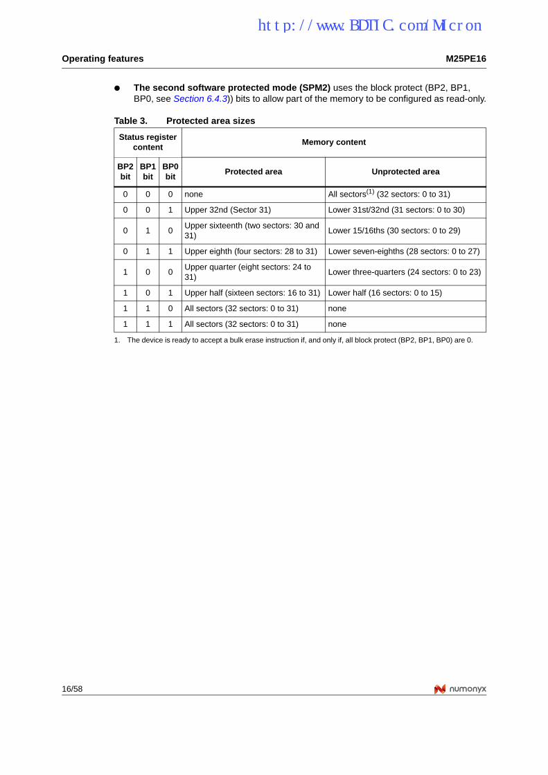
The second software protected mode (SPM2) uses the block protect (BP2, BP1, BP0, see Section 6.4.3)) bits to allow part of the memory to be configured as read-only.
Table 3. Protected area sizes
Status register content
Memory content
BP2 bit
BP1 bit
BP0 bit
Protected area Unprotected area
0 0 0 none All sectors(1) (32 sectors: 0 to 31)
1. The device is ready to accept a bulk erase instruction if, and only if, all block protect (BP2, BP1, BP0) are 0.
0 0 1 Upper 32nd (Sector 31) Lower 31st/32nd (31 sectors: 0 to 30)
0 1 0 Upper sixteenth (two sectors: 30 and 31)
Lower 15/16ths (30 sectors: 0 to 29)
0 1 1 Upper eighth (four sectors: 28 to 31) Lower seven-eighths (28 sectors: 0 to 27)
1 0 0 Upper quarter (eight sectors: 24 to 31)
Lower three-quarters (24 sectors: 0 to 23)
1 0 1 Upper half (sixteen sectors: 16 to 31) Lower half (16 sectors: 0 to 15)
1 1 0 All sectors (32 sectors: 0 to 31) none
1 1 1 All sectors (32 sectors: 0 to 31) none
http://www.BDTIC.com/Micron
M25PE16 Memory organization
17/58
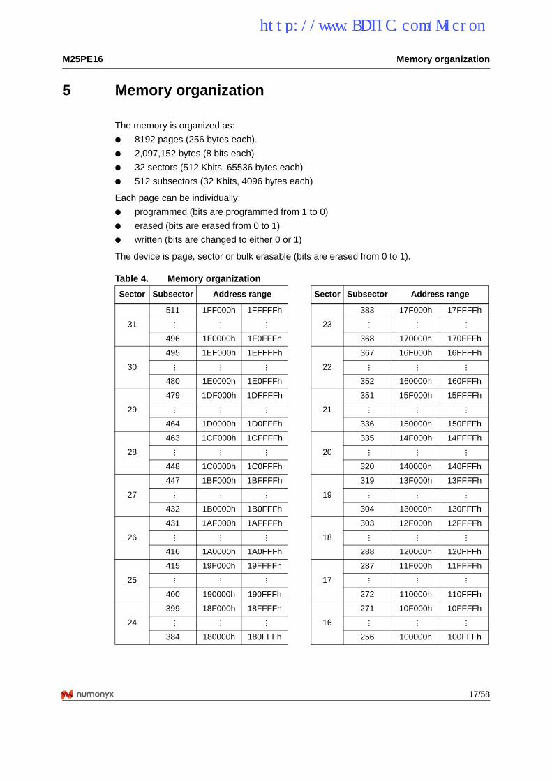
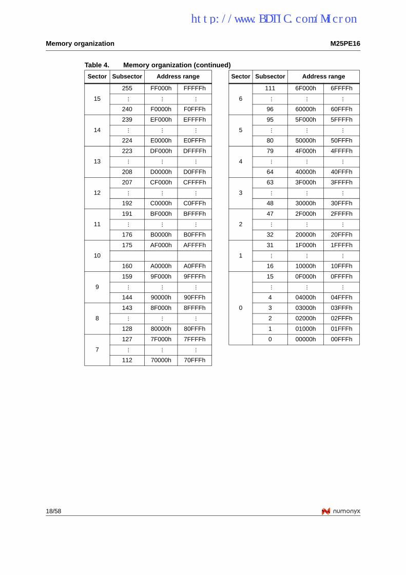
5 Memory organization
The memory is organized as:
8192 pages (256 bytes each).
2,097,152 bytes (8 bits each)
32 sectors (512 Kbits, 65536 bytes each)
512 subsectors (32 Kbits, 4096 bytes each)
Each page can be individually:
programmed (bits are programmed from 1 to 0)
erased (bits are erased from 0 to 1)
written (bits are changed to either 0 or 1)
The device is page, sector or bulk erasable (bits are erased from 0 to 1).
Table 4. Memory organization
Sector Subsector Address range Sector Subsector Address range
31
511 1FF000h 1FFFFFh
23
383 17F000h 17FFFFh
... ... ... ... ... ...
496 1F0000h 1F0FFFh 368 170000h 170FFFh
30
495 1EF000h 1EFFFFh
22
367 16F000h 16FFFFh
... ... ... ... ... ...
480 1E0000h 1E0FFFh 352 160000h 160FFFh
29
479 1DF000h 1DFFFFh
21
351 15F000h 15FFFFh
... ... ... ... ... ...
464 1D0000h 1D0FFFh 336 150000h 150FFFh
28
463 1CF000h 1CFFFFh
20
335 14F000h 14FFFFh
... ... ... ... ... ...448 1C0000h 1C0FFFh 320 140000h 140FFFh
27
447 1BF000h 1BFFFFh
19
319 13F000h 13FFFFh
... ... ... ... ... ...
432 1B0000h 1B0FFFh 304 130000h 130FFFh
26
431 1AF000h 1AFFFFh
18
303 12F000h 12FFFFh
... ... ... ... ... ...
416 1A0000h 1A0FFFh 288 120000h 120FFFh
25
415 19F000h 19FFFFh
17
287 11F000h 11FFFFh
... ... ... ... ... ...
400 190000h 190FFFh 272 110000h 110FFFh
24
399 18F000h 18FFFFh
16
271 10F000h 10FFFFh
... ... ... ... ... ...
384 180000h 180FFFh 256 100000h 100FFFh
http://www.BDTIC.com/Micron
Memory organization M25PE16
18/58
15
255 FF000h FFFFFh
6
111 6F000h 6FFFFh
... ... ... ... ... ...
240 F0000h F0FFFh 96 60000h 60FFFh
14
239 EF000h EFFFFh
5
95 5F000h 5FFFFh... ... ... ... ... ...
224 E0000h E0FFFh 80 50000h 50FFFh
13
223 DF000h DFFFFh
4
79 4F000h 4FFFFh
... ... ... ... ... ...
208 D0000h D0FFFh 64 40000h 40FFFh
12
207 CF000h CFFFFh
3
63 3F000h 3FFFFh
... ... ... ... ... ...
192 C0000h C0FFFh 48 30000h 30FFFh
11
191 BF000h BFFFFh
2
47 2F000h 2FFFFh
... ... ... ... ... ...
176 B0000h B0FFFh 32 20000h 20FFFh
10
175 AF000h AFFFFh
1
31 1F000h 1FFFFh
... ... ...
160 A0000h A0FFFh 16 10000h 10FFFh
9
159 9F000h 9FFFFh
0
15 0F000h 0FFFFh
... ... ... ... ... ...
144 90000h 90FFFh 4 04000h 04FFFh
8
143 8F000h 8FFFFh 3 03000h 03FFFh
... ... ... 2 02000h 02FFFh
128 80000h 80FFFh 1 01000h 01FFFh
7
127 7F000h 7FFFFh 0 00000h 00FFFh
... ... ...
112 70000h 70FFFh
Table 4. Memory organization (continued)
Sector Subsector Address range Sector Subsector Address range
http://www.BDTIC.com/Micron
M25PE16 Memory organization
19/58
Figure 5. Block diagram
AI12346c
S
W Control logicHigh voltage
generator
I/O shift register
Address registerand counter
256-bytedata buffer
256 bytes (page size)
X decoder
Y d
ecod
er
C
D
Q
Statusregister
00000h
1FFFFFh
000FFh
Reset
Whole memory array can be made read-only on a64-Kbyte basis through thelock registers
Size of theread-only
memory area
http://www.BDTIC.com/Micron
Instructions M25PE16
20/58
6 Instructions
All instructions, addresses and data are shifted in and out of the device, most significant bit first.
Serial data input (D) is sampled on the first rising edge of Serial Clock (C) after Chip Select (S) is driven Low. Then, the one-byte instruction code must be shifted in to the device, most significant bit first, on serial data input (D), each bit being latched on the rising edges of Serial Clock (C).
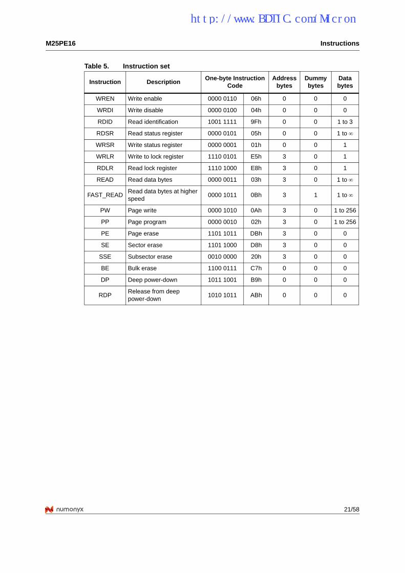
The instruction set is listed in Table 5.
Every instruction sequence starts with a one-byte instruction code. Depending on the instruction, this might be followed by address bytes, or by data bytes, or by both or none.
In the case of a read data bytes (READ), read data bytes at higher speed (Fast_Read), read identification (RDID), read status register (RDSR), or read lock register (RDLR) instruction, the shifted-in instruction sequence is followed by a data-out sequence. Chip Select (S) can be driven High after any bit of the data-out sequence is being shifted out.
In the case of a page write (PW), page program (PP), write to lock register (WRLR), page erase (PE), sector erase (SE), subsector erase (SSE), bulk erase (BE), write status register (WRSR), write enable (WREN), write disable (WRDI), deep power-down (DP) or release from deep power-down (RDP) instruction, Chip Select (S) must be driven High exactly at a byte boundary, otherwise the instruction is rejected, and is not executed. That is, Chip Select (S) must driven High when the number of clock pulses after Chip Select (S) being driven Low is an exact multiple of eight.
All attempts to access the memory array during a write cycle, program cycle or erase cycle are ignored, and the internal write cycle, program cycle or erase cycle continues unaffected.
http://www.BDTIC.com/Micron
M25PE16 Instructions
21/58
Table 5. Instruction set
Instruction Description One-byte Instruction
CodeAddress
bytesDummy bytes
Data bytes
WREN Write enable 0000 0110 06h 0 0 0
WRDI Write disable 0000 0100 04h 0 0 0
RDID Read identification 1001 1111 9Fh 0 0 1 to 3
RDSR Read status register 0000 0101 05h 0 0 1 to ∞
WRSR Write status register 0000 0001 01h 0 0 1
WRLR Write to lock register 1110 0101 E5h 3 0 1
RDLR Read lock register 1110 1000 E8h 3 0 1
READ Read data bytes 0000 0011 03h 3 0 1 to ∞
FAST_READ Read data bytes at higher speed
0000 1011 0Bh 3 1 1 to ∞
PW Page write 0000 1010 0Ah 3 0 1 to 256
PP Page program 0000 0010 02h 3 0 1 to 256
PE Page erase 1101 1011 DBh 3 0 0
SE Sector erase 1101 1000 D8h 3 0 0
SSE Subsector erase 0010 0000 20h 3 0 0
BE Bulk erase 1100 0111 C7h 0 0 0
DP Deep power-down 1011 1001 B9h 0 0 0
RDP Release from deep power-down
1010 1011 ABh 0 0 0
http://www.BDTIC.com/Micron
Instructions M25PE16
22/58
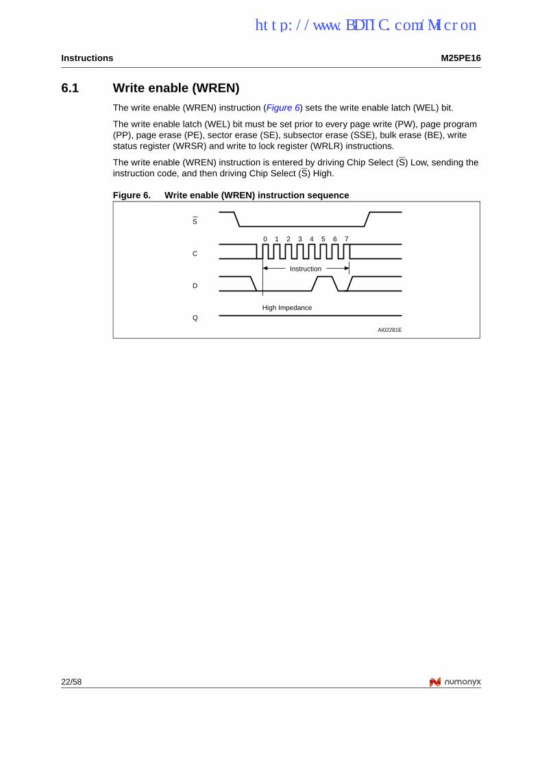
6.1 Write enable (WREN)The write enable (WREN) instruction (Figure 6) sets the write enable latch (WEL) bit.
The write enable latch (WEL) bit must be set prior to every page write (PW), page program (PP), page erase (PE), sector erase (SE), subsector erase (SSE), bulk erase (BE), write status register (WRSR) and write to lock register (WRLR) instructions.
The write enable (WREN) instruction is entered by driving Chip Select (S) Low, sending the instruction code, and then driving Chip Select (S) High.
Figure 6. Write enable (WREN) instruction sequence
C
D
AI02281E
S
Q
21 3 4 5 6 7
High Impedance
0
Instruction
http://www.BDTIC.com/Micron
M25PE16 Instructions
23/58
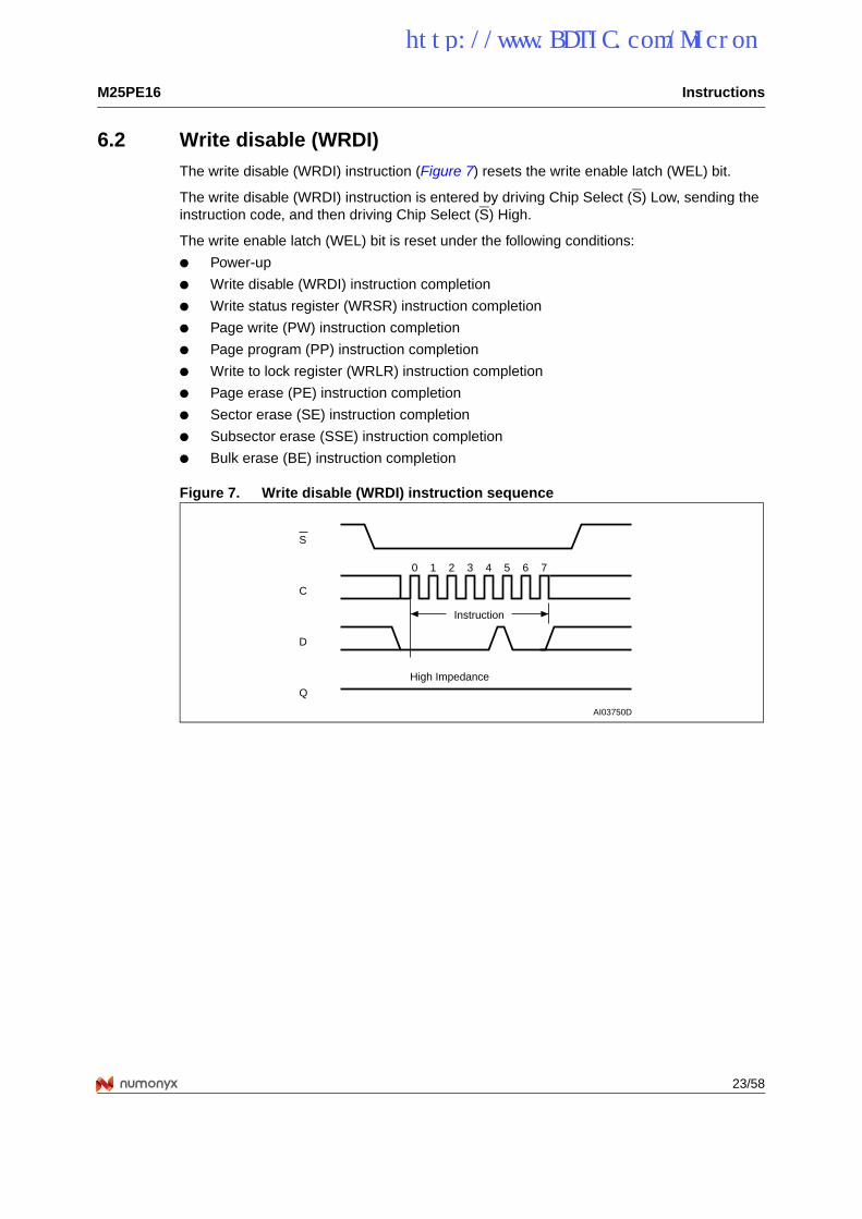
6.2 Write disable (WRDI)The write disable (WRDI) instruction (Figure 7) resets the write enable latch (WEL) bit.
The write disable (WRDI) instruction is entered by driving Chip Select (S) Low, sending the instruction code, and then driving Chip Select (S) High.
The write enable latch (WEL) bit is reset under the following conditions:
Power-up
Write disable (WRDI) instruction completion
Write status register (WRSR) instruction completion
Page write (PW) instruction completion
Page program (PP) instruction completion
Write to lock register (WRLR) instruction completion
Page erase (PE) instruction completion
Sector erase (SE) instruction completion
Subsector erase (SSE) instruction completion
Bulk erase (BE) instruction completion
Figure 7. Write disable (WRDI) instruction sequence
C
D
AI03750D
S
Q
21 3 4 5 6 7
High Impedance
0
Instruction
http://www.BDTIC.com/Micron
Instructions M25PE16
24/58
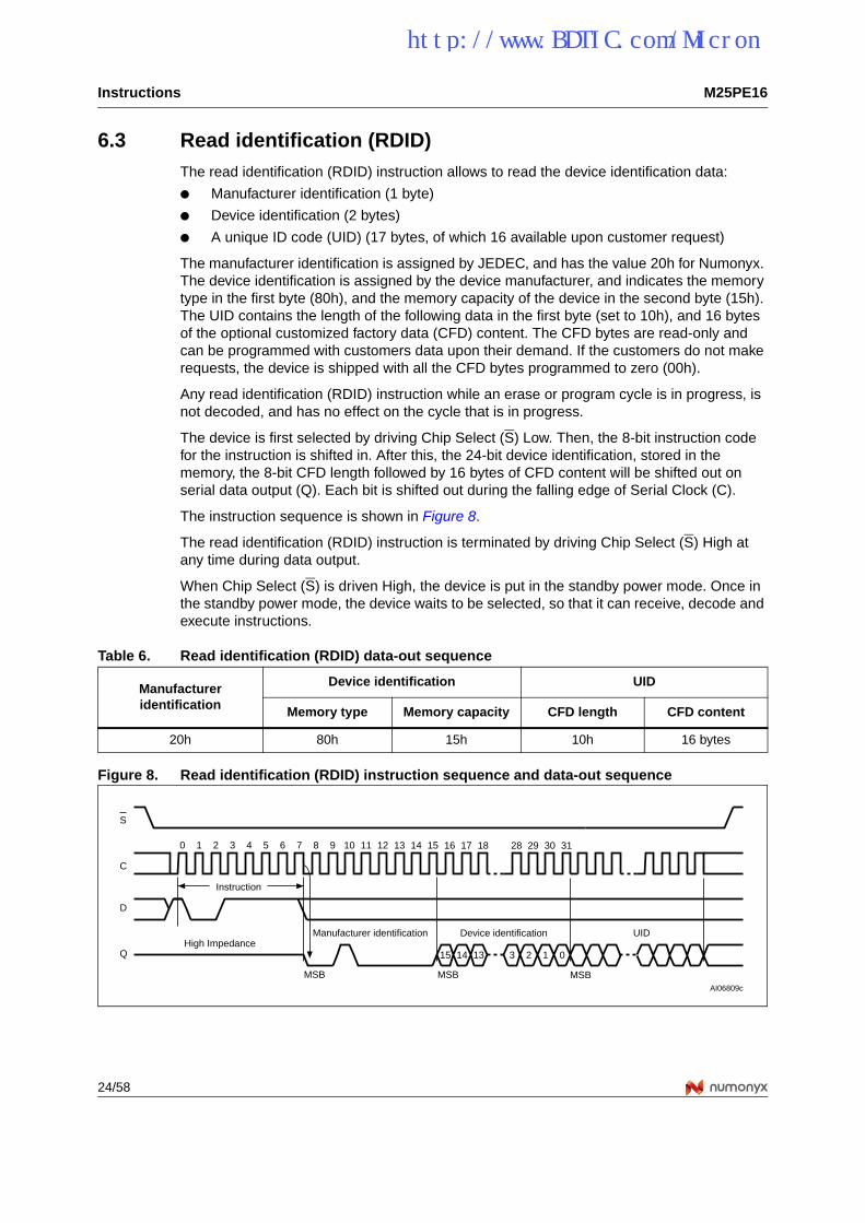
6.3 Read identification (RDID)The read identification (RDID) instruction allows to read the device identification data:
Manufacturer identification (1 byte)
Device identification (2 bytes)
A unique ID code (UID) (17 bytes, of which 16 available upon customer request)
The manufacturer identification is assigned by JEDEC, and has the value 20h for Numonyx. The device identification is assigned by the device manufacturer, and indicates the memory type in the first byte (80h), and the memory capacity of the device in the second byte (15h). The UID contains the length of the following data in the first byte (set to 10h), and 16 bytes of the optional customized factory data (CFD) content. The CFD bytes are read-only and can be programmed with customers data upon their demand. If the customers do not make requests, the device is shipped with all the CFD bytes programmed to zero (00h).
Any read identification (RDID) instruction while an erase or program cycle is in progress, is not decoded, and has no effect on the cycle that is in progress.
The device is first selected by driving Chip Select (S) Low. Then, the 8-bit instruction code for the instruction is shifted in. After this, the 24-bit device identification, stored in the memory, the 8-bit CFD length followed by 16 bytes of CFD content will be shifted out on serial data output (Q). Each bit is shifted out during the falling edge of Serial Clock (C).
The instruction sequence is shown in Figure 8.
The read identification (RDID) instruction is terminated by driving Chip Select (S) High at any time during data output.
When Chip Select (S) is driven High, the device is put in the standby power mode. Once in the standby power mode, the device waits to be selected, so that it can receive, decode and execute instructions.
Figure 8. Read identification (RDID) instruction sequence and data-out sequence
Table 6. Read identification (RDID) data-out sequence
Manufacturer identification
Device identification UID
Memory type Memory capacity CFD length CFD content
20h 80h 15h 10h 16 bytes
C
D
S
21 3 4 5 6 7 8 9 10 11 12 13 14 15
Instruction
0
AI06809c
Q
Manufacturer identificationHigh Impedance
MSB
Device identification
MSB
15 14 13 3 2 1 0
16 17 18 28 29 30 31
MSB
UID
http://www.BDTIC.com/Micron
M25PE16 Instructions
25/58
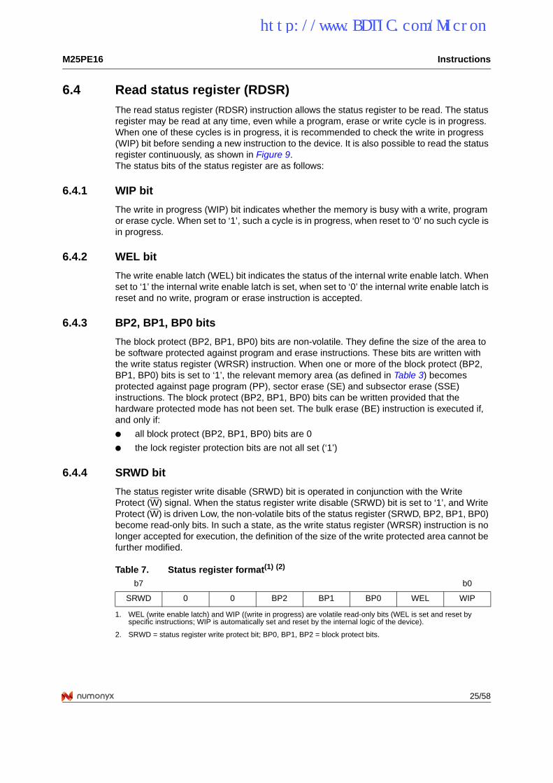
6.4 Read status register (RDSR)The read status register (RDSR) instruction allows the status register to be read. The status register may be read at any time, even while a program, erase or write cycle is in progress. When one of these cycles is in progress, it is recommended to check the write in progress (WIP) bit before sending a new instruction to the device. It is also possible to read the status register continuously, as shown in Figure 9.The status bits of the status register are as follows:
6.4.1 WIP bit
The write in progress (WIP) bit indicates whether the memory is busy with a write, program or erase cycle. When set to ‘1’, such a cycle is in progress, when reset to ‘0’ no such cycle is in progress.
6.4.2 WEL bit
The write enable latch (WEL) bit indicates the status of the internal write enable latch. When set to ‘1’ the internal write enable latch is set, when set to ‘0’ the internal write enable latch is reset and no write, program or erase instruction is accepted.
6.4.3 BP2, BP1, BP0 bits
The block protect (BP2, BP1, BP0) bits are non-volatile. They define the size of the area to be software protected against program and erase instructions. These bits are written with the write status register (WRSR) instruction. When one or more of the block protect (BP2, BP1, BP0) bits is set to ‘1’, the relevant memory area (as defined in Table 3) becomes protected against page program (PP), sector erase (SE) and subsector erase (SSE) instructions. The block protect (BP2, BP1, BP0) bits can be written provided that the hardware protected mode has not been set. The bulk erase (BE) instruction is executed if, and only if:
all block protect (BP2, BP1, BP0) bits are 0
the lock register protection bits are not all set (‘1’)
6.4.4 SRWD bit
The status register write disable (SRWD) bit is operated in conjunction with the Write Protect (W) signal. When the status register write disable (SRWD) bit is set to ‘1’, and Write Protect (W) is driven Low, the non-volatile bits of the status register (SRWD, BP2, BP1, BP0) become read-only bits. In such a state, as the write status register (WRSR) instruction is no longer accepted for execution, the definition of the size of the write protected area cannot be further modified.
Table 7. Status register format(1) (2)
1. WEL (write enable latch) and WIP ((write in progress) are volatile read-only bits (WEL is set and reset by specific instructions; WIP is automatically set and reset by the internal logic of the device).
2. SRWD = status register write protect bit; BP0, BP1, BP2 = block protect bits.
b7 b0
SRWD 0 0 BP2 BP1 BP0 WEL WIP
http://www.BDTIC.com/Micron
Instructions M25PE16
26/58
Figure 9. Read status register (RDSR) instruction sequence and data-out sequence
C
D
S
21 3 4 5 6 7 8 9 10 11 12 13 14 15
Instruction
0
AI02031E
Q 7 6 5 4 3 2 1 0
Status register outHigh Impedance
MSB
7 6 5 4 3 2 1 0
Status register out
MSB
7
http://www.BDTIC.com/Micron
M25PE16 Instructions
27/58
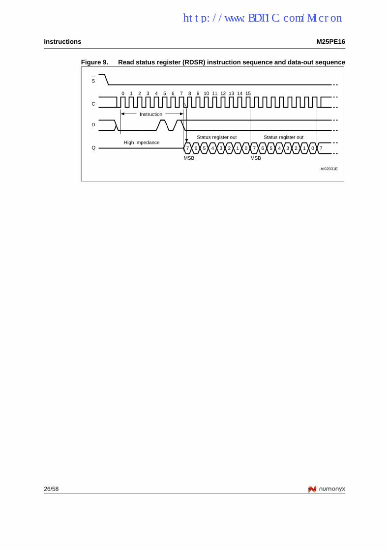
6.5 Write status register (WRSR)The write status register (WRSR) instruction allows new values to be written to the status register. Before it can be accepted, a write enable (WREN) instruction must previously have been executed. After the write enable (WREN) instruction has been decoded and executed, the device sets the write enable latch (WEL).
The write status register (WRSR) instruction is entered by driving Chip Select (S) Low, followed by the instruction code and the data byte on serial data input (D).
The instruction sequence is shown in Figure 10.
The write status register (WRSR) instruction has no effect on b6, b5, b1 and b0 of the status register. b6 and b5 are always read as 0.
Chip Select (S) must be driven High after the eighth bit of the data byte has been latched in. If not, the write status register (WRSR) instruction is not executed. As soon as Chip Select (S) is driven High, the self-timed write status register cycle (whose duration is tW) is initiated. While the write status register cycle is in progress, the status register may still be read to check the value of the write in progress (WIP) bit. The write in progress (WIP) bit is 1 during the self-timed write status register cycle, and is 0 when it is completed. When the cycle is completed, the write enable latch (WEL) is reset.
The write status register (WRSR) instruction allows the user to change the values of the block protect (BP2, BP1, BP0) bits, to define the size of the area that is to be treated as read-only, as defined in Table 3. The write status register (WRSR) instruction also allows the user to set or reset the status register write disable (SRWD) bit in accordance with the Write Protect (W) signal (see Section 6.4.4).
If a write status register (WRSR) instruction is interrupted by a Reset Low pulse, the internal cycle of the write status register operation (whose duration is tW) is first completed (provided that the supply voltage VCC remains within the operating range). After that the device enters the reset mode (see also Table 12: Device status after a Reset Low pulse and Table 21: Timings after a Reset Low pulse).
Figure 10. Write status register (WRSR) instruction sequence
C
D
AI02282D
S
Q
21 3 4 5 6 7 8 9 10 11 12 13 14 15
High Impedance
Instruction Statusregister in
0
7 6 5 4 3 2 01
MSB
http://www.BDTIC.com/Micron
Instructions M25PE16
28/58
The protection features of the device are summarized in Table 8.
When the status register write disable (SRWD) bit of the status register is 0 (its initial delivery state), it is possible to write to the status register provided that the write enable latch (WEL) bit has previously been set by a write enable (WREN) instruction, regardless of the whether Write Protect (W) is driven High or Low.
When the status register write disable (SRWD) bit of the status register is set to ‘1’, two cases need to be considered, depending on the state of Write Protect (W):
If Write Protect (W) is driven High, it is possible to write to the status register provided that the write enable latch (WEL) bit has previously been set by a write enable (WREN) instruction.
If Write Protect (W) is driven Low, it is not possible to write to the status register even if the write enable latch (WEL) bit has previously been set by a write enable (WREN) instruction. Attempts to write to the status register are rejected, and are not accepted for execution. As a consequence, all the data bytes in the memory area that are software protected (SPM2) by the block protect (BP2, BP1, BP0) bits of the status register, are also hardware protected against data modification.
Regardless of the order of the two events, the hardware protected mode (HPM) can be entered:
by setting the status register write disable (SRWD) bit after driving Write Protect (W) Low
or by driving Write Protect (W) Low after setting the status register write disable (SRWD) bit.
The only way to exit the hardware protected mode (HPM) once entered is to pull Write Protect (W) High.
If Write Protect (W) is permanently tied High, the hardware protected mode (HPM) can never be activated, and only the software protected mode (SPM2), using the block protect (BP2, BP1, BP0) bits of the status register, can be used.
Table 8. Protection modes
W signal
SRWD bit
ModeWrite protection of the
status register
Memory content
Protected area(1)
1. As defined by the values in the block protect (BP2, BP1, BP0) bits of the status register, as shown in Table 3.
Unprotected area(1)
1 0Second software protected (SPM2)
Status Register is Writable (if the WREN instruction has set the WEL bit)
The values in the SRWD, BP2, BP1 and BP0 bits can be changed
Protected against page program,
sector erase and bulk erase
Ready to accept page program and
sector erase instructions
0 0
1 1
0 1Hardware protected
(HPM)
Status register is hardware write protected
The values in the SRWD, BP2, BP1 and BP0 bits cannot be changed
Protected against page program,
sector erase and bulk erase
Ready to accept page program and
sector erase instructions
http://www.BDTIC.com/Micron
M25PE16 Instructions
29/58
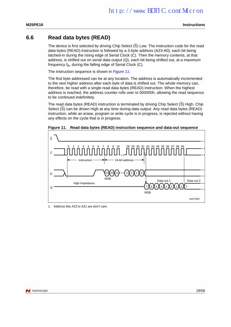
6.6 Read data bytes (READ)The device is first selected by driving Chip Select (S) Low. The instruction code for the read data bytes (READ) instruction is followed by a 3-byte address (A23-A0), each bit being latched-in during the rising edge of Serial Clock (C). Then the memory contents, at that address, is shifted out on serial data output (Q), each bit being shifted out, at a maximum frequency fR, during the falling edge of Serial Clock (C).
The instruction sequence is shown in Figure 11.
The first byte addressed can be at any location. The address is automatically incremented to the next higher address after each byte of data is shifted out. The whole memory can, therefore, be read with a single read data bytes (READ) instruction. When the highest address is reached, the address counter rolls over to 000000h, allowing the read sequence to be continued indefinitely.
The read data bytes (READ) instruction is terminated by driving Chip Select (S) High. Chip Select (S) can be driven High at any time during data output. Any read data bytes (READ) instruction, while an erase, program or write cycle is in progress, is rejected without having any effects on the cycle that is in progress.
Figure 11. Read data bytes (READ) instruction sequence and data-out sequence
1. Address bits A23 to A21 are don’t care.
C
D
AI03748D
S
Q
23
21 3 4 5 6 7 8 9 10 28 29 30 31 32 33 34 35
22 21 3 2 1 0
36 37 38
7 6 5 4 3 1 70High Impedance
Data out 1
Instruction 24-bit address
0
MSB
MSB
2
39
Data out 2
http://www.BDTIC.com/Micron
Instructions M25PE16
30/58
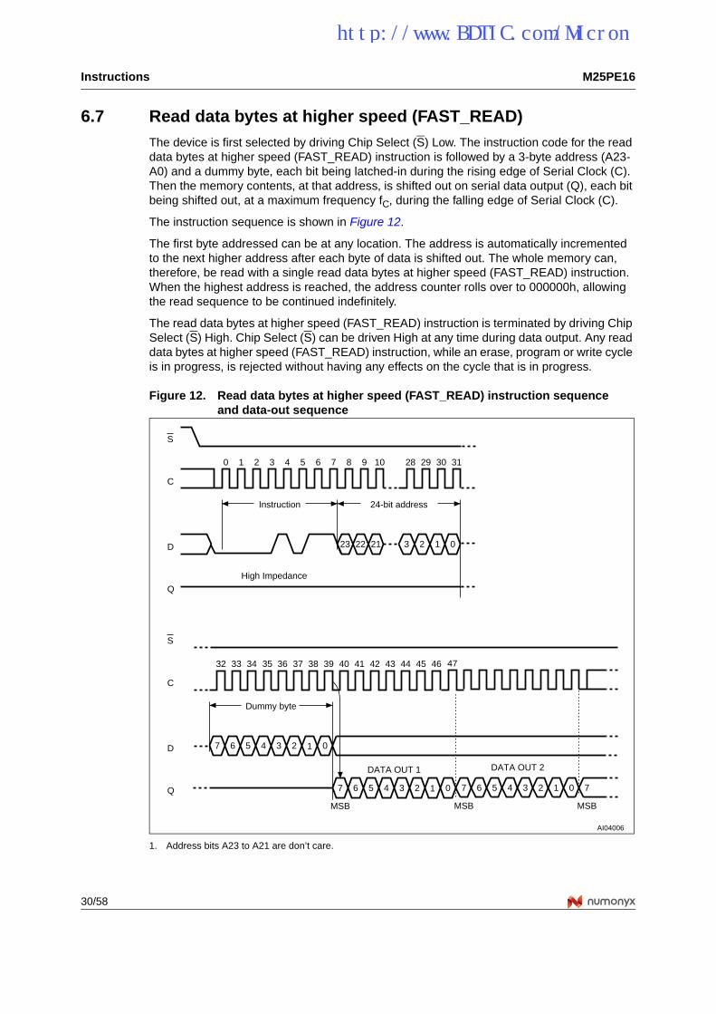
6.7 Read data bytes at higher speed (FAST_READ)The device is first selected by driving Chip Select (S) Low. The instruction code for the read data bytes at higher speed (FAST_READ) instruction is followed by a 3-byte address (A23-A0) and a dummy byte, each bit being latched-in during the rising edge of Serial Clock (C). Then the memory contents, at that address, is shifted out on serial data output (Q), each bit being shifted out, at a maximum frequency fC, during the falling edge of Serial Clock (C).
The instruction sequence is shown in Figure 12.
The first byte addressed can be at any location. The address is automatically incremented to the next higher address after each byte of data is shifted out. The whole memory can, therefore, be read with a single read data bytes at higher speed (FAST_READ) instruction. When the highest address is reached, the address counter rolls over to 000000h, allowing the read sequence to be continued indefinitely.
The read data bytes at higher speed (FAST_READ) instruction is terminated by driving Chip Select (S) High. Chip Select (S) can be driven High at any time during data output. Any read data bytes at higher speed (FAST_READ) instruction, while an erase, program or write cycle is in progress, is rejected without having any effects on the cycle that is in progress.
Figure 12. Read data bytes at higher speed (FAST_READ) instruction sequenceand data-out sequence
1. Address bits A23 to A21 are don’t care.
C
D
AI04006
S
Q
23
21 3 4 5 6 7 8 9 10 28 29 30 31
22 21 3 2 1 0
High Impedance
Instruction 24-bit address
0
C
D
S
Q
32 33 34 36 37 38 39 40 41 42 43 44 45 46
7 6 5 4 3 2 01
DATA OUT 1
Dummy byte
MSB
7 6 5 4 3 2 1 0
DATA OUT 2
MSB MSB
7
47
7 6 5 4 3 2 01
35
http://www.BDTIC.com/Micron
M25PE16 Instructions
31/58
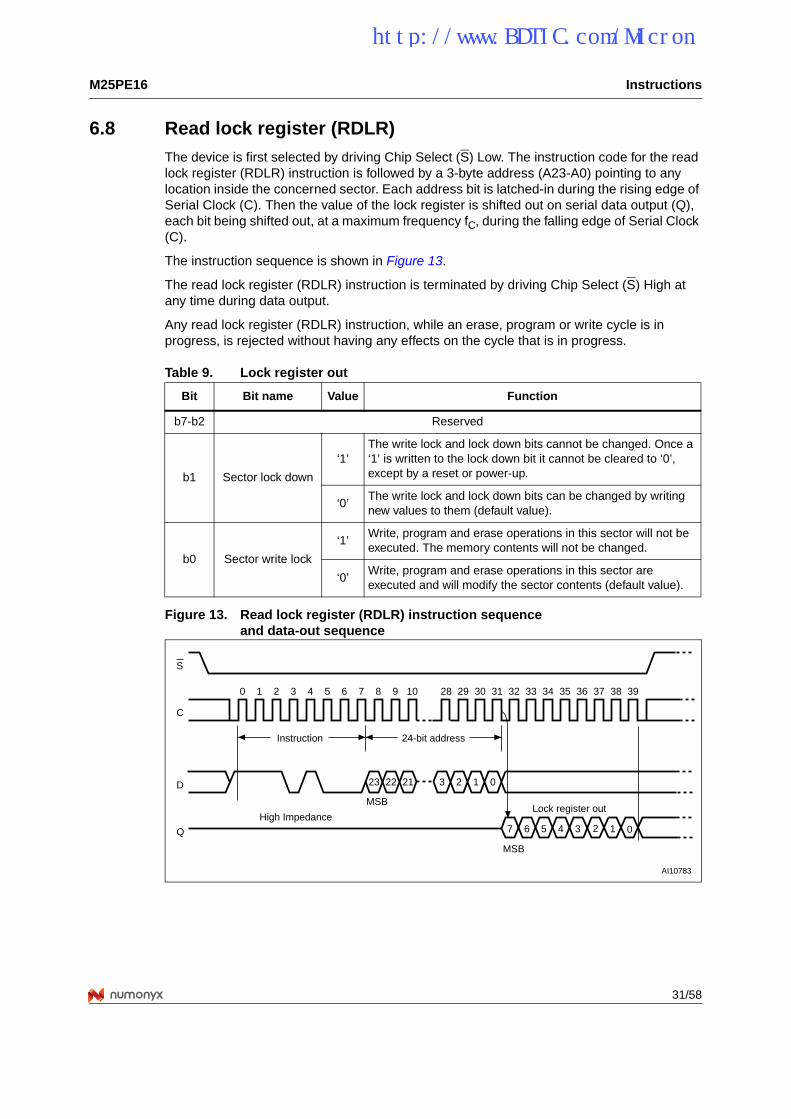
6.8 Read lock register (RDLR)The device is first selected by driving Chip Select (S) Low. The instruction code for the read lock register (RDLR) instruction is followed by a 3-byte address (A23-A0) pointing to any location inside the concerned sector. Each address bit is latched-in during the rising edge of Serial Clock (C). Then the value of the lock register is shifted out on serial data output (Q), each bit being shifted out, at a maximum frequency fC, during the falling edge of Serial Clock (C).
The instruction sequence is shown in Figure 13.
The read lock register (RDLR) instruction is terminated by driving Chip Select (S) High at any time during data output.
Any read lock register (RDLR) instruction, while an erase, program or write cycle is in progress, is rejected without having any effects on the cycle that is in progress.
Figure 13. Read lock register (RDLR) instruction sequenceand data-out sequence
Table 9. Lock register out
Bit Bit name Value Function
b7-b2 Reserved
b1 Sector lock down
‘1’The write lock and lock down bits cannot be changed. Once a ‘1’ is written to the lock down bit it cannot be cleared to ‘0’, except by a reset or power-up.
‘0’The write lock and lock down bits can be changed by writing new values to them (default value).
b0 Sector write lock
‘1’Write, program and erase operations in this sector will not be executed. The memory contents will not be changed.
‘0’Write, program and erase operations in this sector are executed and will modify the sector contents (default value).
C
D
AI10783
S
Q
23
21 3 4 5 6 7 8 9 10 28 29 30 31 32 33 34 35
22 21 3 2 1 0
36 37 38
7 6 5 4 3 1 0High Impedance
Lock register out
Instruction 24-bit address
0
MSB
MSB
2
39
http://www.BDTIC.com/Micron
Instructions M25PE16
32/58
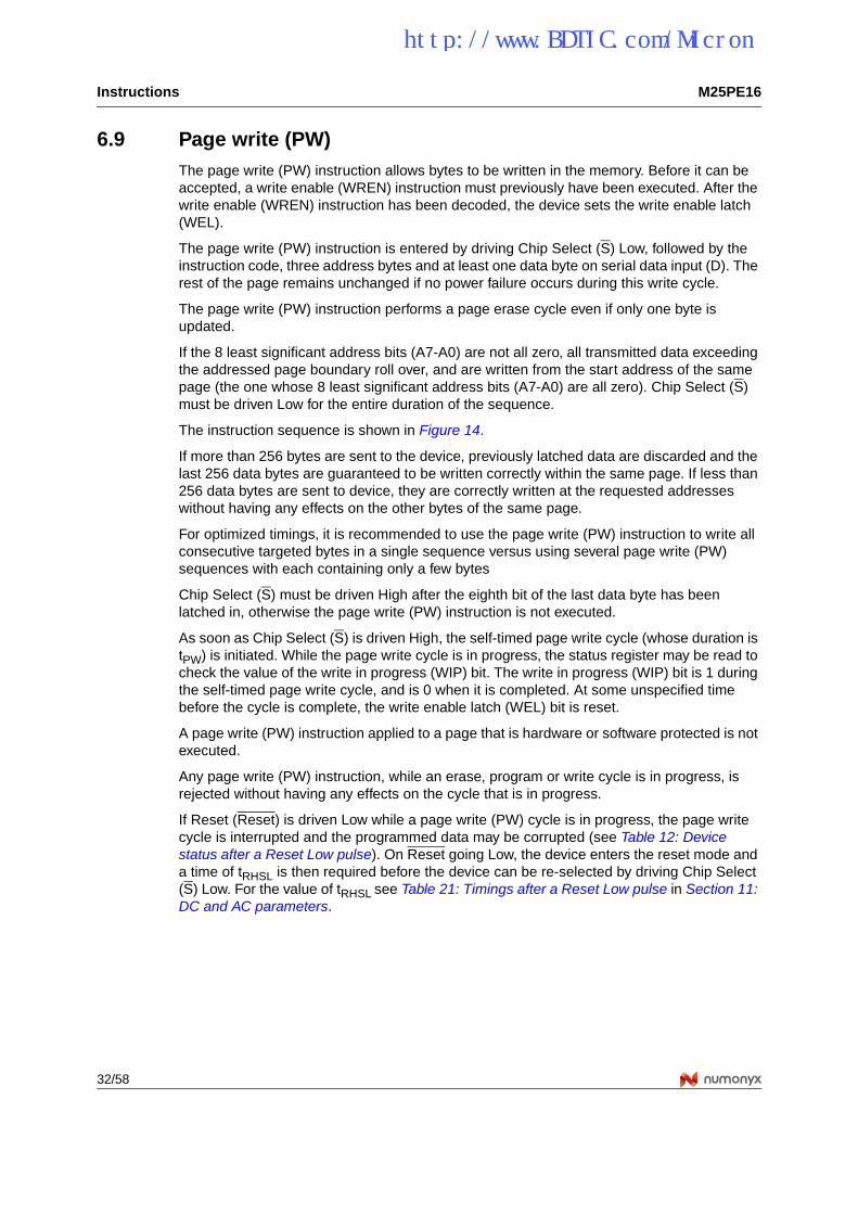
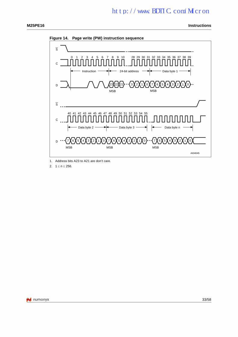
6.9 Page write (PW)The page write (PW) instruction allows bytes to be written in the memory. Before it can be accepted, a write enable (WREN) instruction must previously have been executed. After the write enable (WREN) instruction has been decoded, the device sets the write enable latch (WEL).
The page write (PW) instruction is entered by driving Chip Select (S) Low, followed by the instruction code, three address bytes and at least one data byte on serial data input (D). The rest of the page remains unchanged if no power failure occurs during this write cycle.
The page write (PW) instruction performs a page erase cycle even if only one byte is updated.
If the 8 least significant address bits (A7-A0) are not all zero, all transmitted data exceeding the addressed page boundary roll over, and are written from the start address of the same page (the one whose 8 least significant address bits (A7-A0) are all zero). Chip Select (S) must be driven Low for the entire duration of the sequence.
The instruction sequence is shown in Figure 14.
If more than 256 bytes are sent to the device, previously latched data are discarded and the last 256 data bytes are guaranteed to be written correctly within the same page. If less than 256 data bytes are sent to device, they are correctly written at the requested addresses without having any effects on the other bytes of the same page.
For optimized timings, it is recommended to use the page write (PW) instruction to write all consecutive targeted bytes in a single sequence versus using several page write (PW) sequences with each containing only a few bytes
Chip Select (S) must be driven High after the eighth bit of the last data byte has been latched in, otherwise the page write (PW) instruction is not executed.
As soon as Chip Select (S) is driven High, the self-timed page write cycle (whose duration is tPW) is initiated. While the page write cycle is in progress, the status register may be read to check the value of the write in progress (WIP) bit. The write in progress (WIP) bit is 1 during the self-timed page write cycle, and is 0 when it is completed. At some unspecified time before the cycle is complete, the write enable latch (WEL) bit is reset.
A page write (PW) instruction applied to a page that is hardware or software protected is not executed.
Any page write (PW) instruction, while an erase, program or write cycle is in progress, is rejected without having any effects on the cycle that is in progress.
If Reset (Reset) is driven Low while a page write (PW) cycle is in progress, the page write cycle is interrupted and the programmed data may be corrupted (see Table 12: Device status after a Reset Low pulse). On Reset going Low, the device enters the reset mode and a time of tRHSL is then required before the device can be re-selected by driving Chip Select (S) Low. For the value of tRHSL see Table 21: Timings after a Reset Low pulse in Section 11: DC and AC parameters.
http://www.BDTIC.com/Micron
M25PE16 Instructions
33/58
Figure 14. Page write (PW) instruction sequence
1. Address bits A23 to A21 are don’t care.
2. 1 ≤ n ≤ 256.
C
D
AI04045
S
4241 43 44 45 46 47 48 49 50 52 53 54 5540
C
D
S
23
21 3 4 5 6 7 8 9 10 28 29 30 31 32 33 34 35
22 21 3 2 1 0
36 37 38
Instruction 24-bit address
0
7 6 5 4 3 2 01
Data byte 1
39
51
7 6 5 4 3 2 01
Data byte 2
7 6 5 4 3 2 01
Data byte 3 Data byte n
7 6 5 4 3 2 01
MSB MSB
MSB MSB MSB
http://www.BDTIC.com/Micron
Instructions M25PE16
34/58
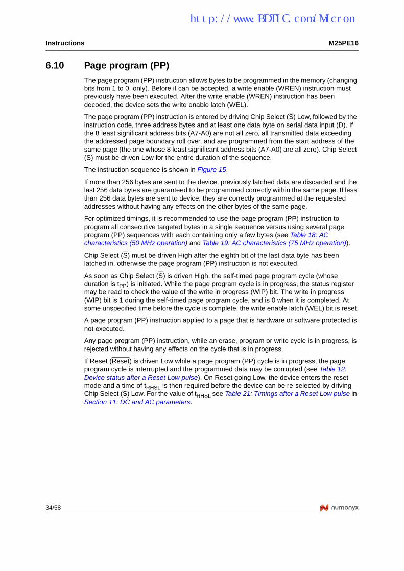
6.10 Page program (PP)The page program (PP) instruction allows bytes to be programmed in the memory (changing bits from 1 to 0, only). Before it can be accepted, a write enable (WREN) instruction must previously have been executed. After the write enable (WREN) instruction has been decoded, the device sets the write enable latch (WEL).
The page program (PP) instruction is entered by driving Chip Select (S) Low, followed by the instruction code, three address bytes and at least one data byte on serial data input (D). If the 8 least significant address bits (A7-A0) are not all zero, all transmitted data exceeding the addressed page boundary roll over, and are programmed from the start address of the same page (the one whose 8 least significant address bits (A7-A0) are all zero). Chip Select (S) must be driven Low for the entire duration of the sequence.
The instruction sequence is shown in Figure 15.
If more than 256 bytes are sent to the device, previously latched data are discarded and the last 256 data bytes are guaranteed to be programmed correctly within the same page. If less than 256 data bytes are sent to device, they are correctly programmed at the requested addresses without having any effects on the other bytes of the same page.
For optimized timings, it is recommended to use the page program (PP) instruction to program all consecutive targeted bytes in a single sequence versus using several page program (PP) sequences with each containing only a few bytes (see Table 18: AC characteristics (50 MHz operation) and Table 19: AC characteristics (75 MHz operation)).
Chip Select (S) must be driven High after the eighth bit of the last data byte has been latched in, otherwise the page program (PP) instruction is not executed.
As soon as Chip Select (S) is driven High, the self-timed page program cycle (whose duration is tPP) is initiated. While the page program cycle is in progress, the status register may be read to check the value of the write in progress (WIP) bit. The write in progress (WIP) bit is 1 during the self-timed page program cycle, and is 0 when it is completed. At some unspecified time before the cycle is complete, the write enable latch (WEL) bit is reset.
A page program (PP) instruction applied to a page that is hardware or software protected is not executed.
Any page program (PP) instruction, while an erase, program or write cycle is in progress, is rejected without having any effects on the cycle that is in progress.
If Reset (Reset) is driven Low while a page program (PP) cycle is in progress, the page program cycle is interrupted and the programmed data may be corrupted (see Table 12: Device status after a Reset Low pulse). On Reset going Low, the device enters the reset mode and a time of tRHSL is then required before the device can be re-selected by driving Chip Select (S) Low. For the value of tRHSL see Table 21: Timings after a Reset Low pulse in Section 11: DC and AC parameters.
http://www.BDTIC.com/Micron
M25PE16 Instructions
35/58
Figure 15. Page program (PP) instruction sequence
1. Address bits A23 to A21 are don’t care.
2. 1 ≤ n ≤ 256.
C
D
AI04044
S
4241 43 44 45 46 47 48 49 50 52 53 54 5540
C
D
S
23
21 3 4 5 6 7 8 9 10 28 29 30 31 32 33 34 35
22 21 3 2 1 0
36 37 38
Instruction 24-bit address
0
7 6 5 4 3 2 01
Data byte 1
39
51
7 6 5 4 3 2 01
Data byte 2
7 6 5 4 3 2 01
Data byte 3 Data byte n
7 6 5 4 3 2 01
MSB MSB
MSB MSB MSB
http://www.BDTIC.com/Micron
Instructions M25PE16
36/58
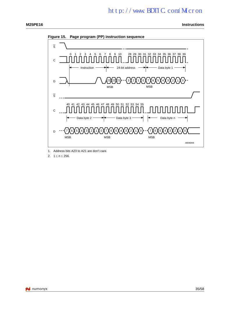
6.11 Write to lock register (WRLR)The write to lock register (WRLR) instruction allows bits to be changed in the lock registers. Before it can be accepted, a write enable (WREN) instruction must previously have been executed. After the write enable (WREN) instruction has been decoded, the device sets the write enable latch (WEL).
The write to lock register (WRLR) instruction is entered by driving Chip Select (S) Low, followed by the instruction code, three address bytes (pointing to any address in the targeted sector and one data byte on serial data input (D). The instruction sequence is shown in Figure 16. Chip Select (S) must be driven High after the eighth bit of the data byte has been latched in, otherwise the write to lock register (WRLR) instruction is not executed.
Lock register bits are volatile, and therefore do not require time to be written. When the write to lock register (WRLR) instruction has been successfully executed, the write enable latch (WEL) bit is reset after a delay time less than tSHSL minimum value.
Any write to lock register (WRLR) instruction, while an erase, program or write cycle is in progress, is rejected without having any effects on the cycle that is in progress.
Figure 16. Write to lock register (WRLR) instruction sequence
Table 10. Lock register in
Sector Bit Value
All sectors
b7-b2 ‘0’
b1 Sector lock down bit value (refer to Table 9)
b0 Sector write lock bit value (refer to Table 9)
AI10784
C
D
S
23
21 3 4 5 6 7 8 9 10 28 29 30 31 32 33 34 35
22 21 3 2 1 0
36 37 38
Instruction 24-bit address
0
7 6 5 4 3 2 01
Lock registerin
39
MSB MSB
http://www.BDTIC.com/Micron
M25PE16 Instructions
37/58
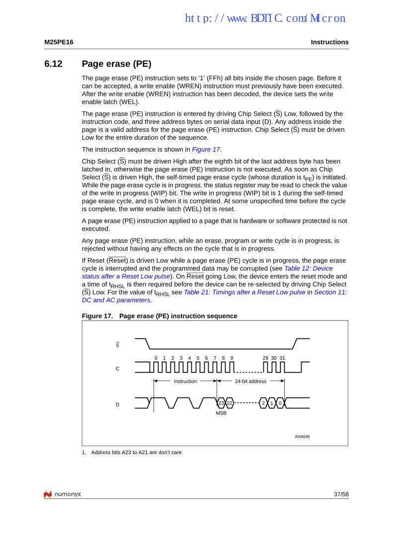
6.12 Page erase (PE)The page erase (PE) instruction sets to ‘1’ (FFh) all bits inside the chosen page. Before it can be accepted, a write enable (WREN) instruction must previously have been executed. After the write enable (WREN) instruction has been decoded, the device sets the write enable latch (WEL).
The page erase (PE) instruction is entered by driving Chip Select (S) Low, followed by the instruction code, and three address bytes on serial data input (D). Any address inside the page is a valid address for the page erase (PE) instruction. Chip Select (S) must be driven Low for the entire duration of the sequence.
The instruction sequence is shown in Figure 17.
Chip Select (S) must be driven High after the eighth bit of the last address byte has been latched in, otherwise the page erase (PE) instruction is not executed. As soon as Chip Select (S) is driven High, the self-timed page erase cycle (whose duration is tPE) is initiated. While the page erase cycle is in progress, the status register may be read to check the value of the write in progress (WIP) bit. The write in progress (WIP) bit is 1 during the self-timed page erase cycle, and is 0 when it is completed. At some unspecified time before the cycle is complete, the write enable latch (WEL) bit is reset.
A page erase (PE) instruction applied to a page that is hardware or software protected is not executed.
Any page erase (PE) instruction, while an erase, program or write cycle is in progress, is rejected without having any effects on the cycle that is in progress.
If Reset (Reset) is driven Low while a page erase (PE) cycle is in progress, the page erase cycle is interrupted and the programmed data may be corrupted (see Table 12: Device status after a Reset Low pulse). On Reset going Low, the device enters the reset mode and a time of tRHSL is then required before the device can be re-selected by driving Chip Select (S) Low. For the value of tRHSL see Table 21: Timings after a Reset Low pulse in Section 11: DC and AC parameters.
Figure 17. Page erase (PE) instruction sequence
1. Address bits A23 to A21 are don’t care.
24-bit address
C
D
AI04046
S
21 3 4 5 6 7 8 9 29 30 31
Instruction
0
23 22 2 01
MSB
http://www.BDTIC.com/Micron
Instructions M25PE16
38/58
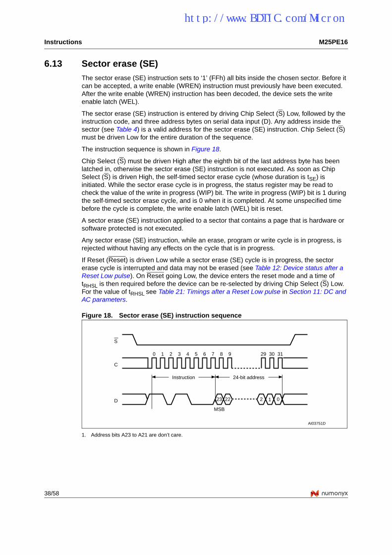
6.13 Sector erase (SE)The sector erase (SE) instruction sets to ‘1’ (FFh) all bits inside the chosen sector. Before it can be accepted, a write enable (WREN) instruction must previously have been executed. After the write enable (WREN) instruction has been decoded, the device sets the write enable latch (WEL).
The sector erase (SE) instruction is entered by driving Chip Select (S) Low, followed by the instruction code, and three address bytes on serial data input (D). Any address inside the sector (see Table 4) is a valid address for the sector erase (SE) instruction. Chip Select (S) must be driven Low for the entire duration of the sequence.
The instruction sequence is shown in Figure 18.
Chip Select (S) must be driven High after the eighth bit of the last address byte has been latched in, otherwise the sector erase (SE) instruction is not executed. As soon as Chip Select (S) is driven High, the self-timed sector erase cycle (whose duration is tSE) is initiated. While the sector erase cycle is in progress, the status register may be read to check the value of the write in progress (WIP) bit. The write in progress (WIP) bit is 1 during the self-timed sector erase cycle, and is 0 when it is completed. At some unspecified time before the cycle is complete, the write enable latch (WEL) bit is reset.
A sector erase (SE) instruction applied to a sector that contains a page that is hardware or software protected is not executed.
Any sector erase (SE) instruction, while an erase, program or write cycle is in progress, is rejected without having any effects on the cycle that is in progress.
If Reset (Reset) is driven Low while a sector erase (SE) cycle is in progress, the sector erase cycle is interrupted and data may not be erased (see Table 12: Device status after a Reset Low pulse). On Reset going Low, the device enters the reset mode and a time of tRHSL is then required before the device can be re-selected by driving Chip Select (S) Low. For the value of tRHSL see Table 21: Timings after a Reset Low pulse in Section 11: DC and AC parameters.
Figure 18. Sector erase (SE) instruction sequence
1. Address bits A23 to A21 are don’t care.
24-bit address
C
D
AI03751D
S
21 3 4 5 6 7 8 9 29 30 31
Instruction
0
23 22 2 01
MSB
http://www.BDTIC.com/Micron
M25PE16 Instructions
39/58
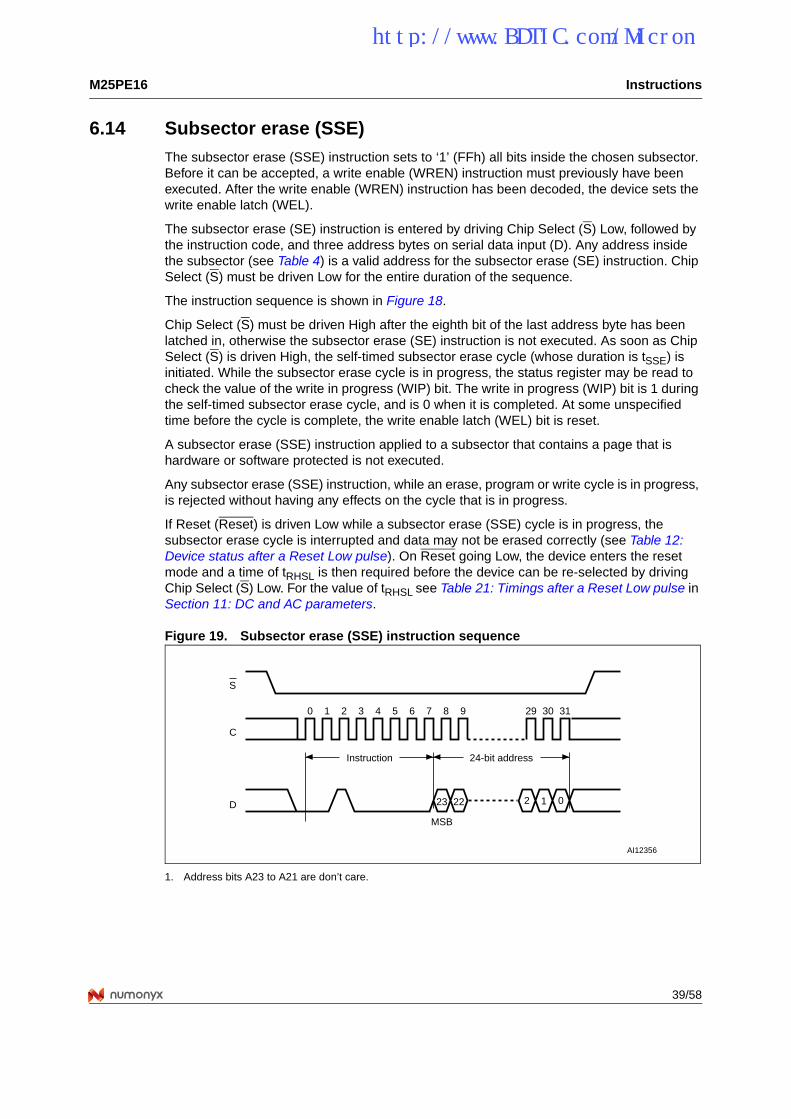
6.14 Subsector erase (SSE)The subsector erase (SSE) instruction sets to ‘1’ (FFh) all bits inside the chosen subsector. Before it can be accepted, a write enable (WREN) instruction must previously have been executed. After the write enable (WREN) instruction has been decoded, the device sets the write enable latch (WEL).
The subsector erase (SE) instruction is entered by driving Chip Select (S) Low, followed by the instruction code, and three address bytes on serial data input (D). Any address inside the subsector (see Table 4) is a valid address for the subsector erase (SE) instruction. Chip Select (S) must be driven Low for the entire duration of the sequence.
The instruction sequence is shown in Figure 18.
Chip Select (S) must be driven High after the eighth bit of the last address byte has been latched in, otherwise the subsector erase (SE) instruction is not executed. As soon as Chip Select (S) is driven High, the self-timed subsector erase cycle (whose duration is tSSE) is initiated. While the subsector erase cycle is in progress, the status register may be read to check the value of the write in progress (WIP) bit. The write in progress (WIP) bit is 1 during the self-timed subsector erase cycle, and is 0 when it is completed. At some unspecified time before the cycle is complete, the write enable latch (WEL) bit is reset.
A subsector erase (SSE) instruction applied to a subsector that contains a page that is hardware or software protected is not executed.
Any subsector erase (SSE) instruction, while an erase, program or write cycle is in progress, is rejected without having any effects on the cycle that is in progress.
If Reset (Reset) is driven Low while a subsector erase (SSE) cycle is in progress, the subsector erase cycle is interrupted and data may not be erased correctly (see Table 12: Device status after a Reset Low pulse). On Reset going Low, the device enters the reset mode and a time of tRHSL is then required before the device can be re-selected by driving Chip Select (S) Low. For the value of tRHSL see Table 21: Timings after a Reset Low pulse in Section 11: DC and AC parameters.
Figure 19. Subsector erase (SSE) instruction sequence
1. Address bits A23 to A21 are don’t care.
24-bit address
C
D
AI12356
S
21 3 4 5 6 7 8 9 29 30 31
Instruction
0
23 22 2 01
MSB
http://www.BDTIC.com/Micron
Instructions M25PE16
40/58
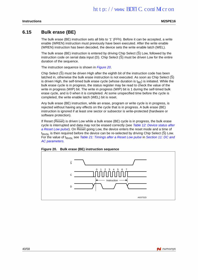
6.15 Bulk erase (BE)The bulk erase (BE) instruction sets all bits to ‘1’ (FFh). Before it can be accepted, a write enable (WREN) instruction must previously have been executed. After the write enable (WREN) instruction has been decoded, the device sets the write enable latch (WEL).
The bulk erase (BE) instruction is entered by driving Chip Select (S) Low, followed by the instruction code on serial data input (D). Chip Select (S) must be driven Low for the entire duration of the sequence.
The instruction sequence is shown in Figure 20.
Chip Select (S) must be driven High after the eighth bit of the instruction code has been latched in, otherwise the bulk erase instruction is not executed. As soon as Chip Select (S) is driven High, the self-timed bulk erase cycle (whose duration is tBE) is initiated. While the bulk erase cycle is in progress, the status register may be read to check the value of the write in progress (WIP) bit. The write in progress (WIP) bit is 1 during the self-timed bulk erase cycle, and is 0 when it is completed. At some unspecified time before the cycle is completed, the write enable latch (WEL) bit is reset.
Any bulk erase (BE) instruction, while an erase, program or write cycle is in progress, is rejected without having any effects on the cycle that is in progress. A bulk erase (BE) instruction is ignored if at least one sector or subsector is write-protected (hardware or software protection).
If Reset (Reset) is driven Low while a bulk erase (BE) cycle is in progress, the bulk erase cycle is interrupted and data may not be erased correctly (see Table 12: Device status after a Reset Low pulse). On Reset going Low, the device enters the reset mode and a time of tRHSL is then required before the device can be re-selected by driving Chip Select (S) Low. For the value of tRHSL see Table 21: Timings after a Reset Low pulse in Section 11: DC and AC parameters.
Figure 20. Bulk erase (BE) instruction sequence
C
D
AI03752D
S
21 3 4 5 6 70
Instruction
http://www.BDTIC.com/Micron
M25PE16 Instructions
41/58
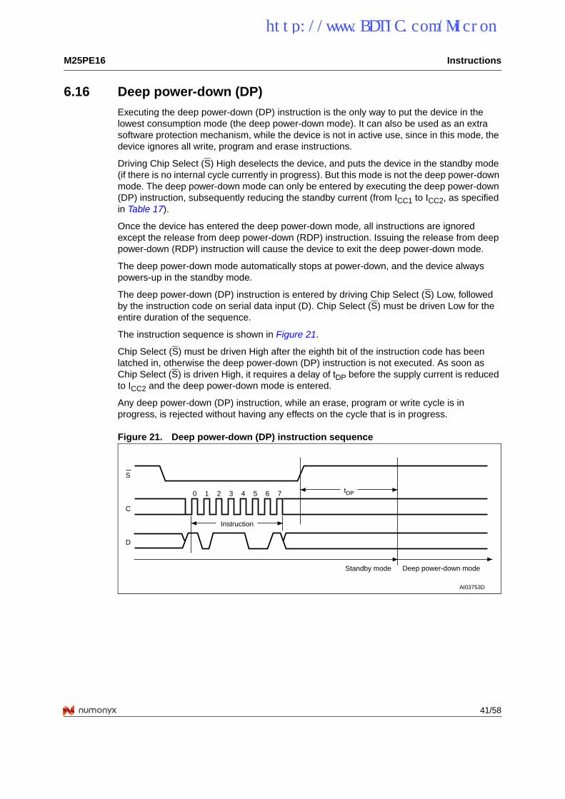
6.16 Deep power-down (DP)Executing the deep power-down (DP) instruction is the only way to put the device in the lowest consumption mode (the deep power-down mode). It can also be used as an extra software protection mechanism, while the device is not in active use, since in this mode, the device ignores all write, program and erase instructions.
Driving Chip Select (S) High deselects the device, and puts the device in the standby mode (if there is no internal cycle currently in progress). But this mode is not the deep power-down mode. The deep power-down mode can only be entered by executing the deep power-down (DP) instruction, subsequently reducing the standby current (from ICC1 to ICC2, as specified in Table 17).
Once the device has entered the deep power-down mode, all instructions are ignored except the release from deep power-down (RDP) instruction. Issuing the release from deep power-down (RDP) instruction will cause the device to exit the deep power-down mode.
The deep power-down mode automatically stops at power-down, and the device always powers-up in the standby mode.
The deep power-down (DP) instruction is entered by driving Chip Select (S) Low, followed by the instruction code on serial data input (D). Chip Select (S) must be driven Low for the entire duration of the sequence.
The instruction sequence is shown in Figure 21.
Chip Select (S) must be driven High after the eighth bit of the instruction code has been latched in, otherwise the deep power-down (DP) instruction is not executed. As soon as Chip Select (S) is driven High, it requires a delay of tDP before the supply current is reduced to ICC2 and the deep power-down mode is entered.
Any deep power-down (DP) instruction, while an erase, program or write cycle is in progress, is rejected without having any effects on the cycle that is in progress.
Figure 21. Deep power-down (DP) instruction sequence
C
D
AI03753D
S
21 3 4 5 6 70 tDP
Deep power-down modeStandby mode
Instruction
http://www.BDTIC.com/Micron
Instructions M25PE16
42/58
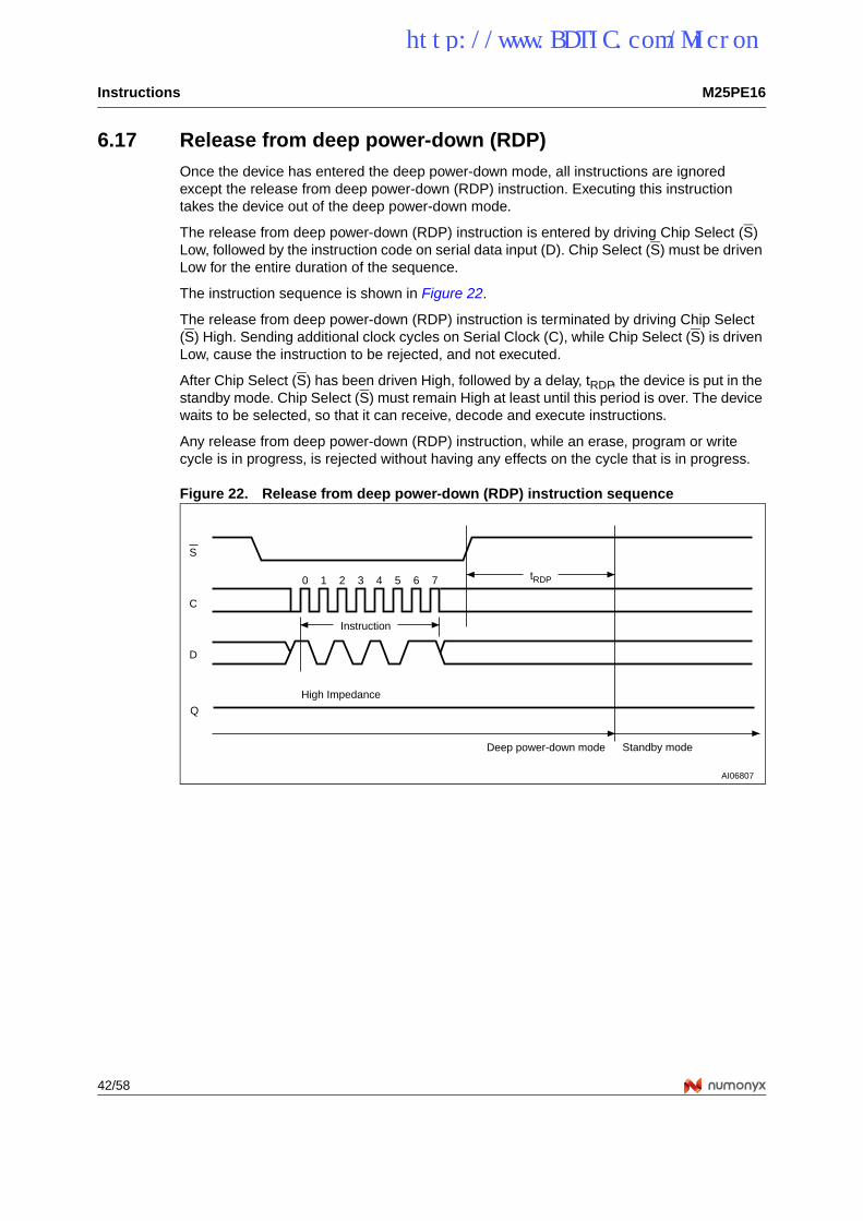
6.17 Release from deep power-down (RDP)Once the device has entered the deep power-down mode, all instructions are ignored except the release from deep power-down (RDP) instruction. Executing this instruction takes the device out of the deep power-down mode.
The release from deep power-down (RDP) instruction is entered by driving Chip Select (S) Low, followed by the instruction code on serial data input (D). Chip Select (S) must be driven Low for the entire duration of the sequence.
The instruction sequence is shown in Figure 22.
The release from deep power-down (RDP) instruction is terminated by driving Chip Select (S) High. Sending additional clock cycles on Serial Clock (C), while Chip Select (S) is driven Low, cause the instruction to be rejected, and not executed.
After Chip Select (S) has been driven High, followed by a delay, tRDP, the device is put in the standby mode. Chip Select (S) must remain High at least until this period is over. The device waits to be selected, so that it can receive, decode and execute instructions.
Any release from deep power-down (RDP) instruction, while an erase, program or write cycle is in progress, is rejected without having any effects on the cycle that is in progress.
Figure 22. Release from deep power-down (RDP) instruction sequence
C
D
AI06807
S
21 3 4 5 6 70 tRDP
Standby modeDeep power-down mode
Q
High Impedance
Instruction
http://www.BDTIC.com/Micron
M25PE16 Power-up and power-down
43/58
7 Power-up and power-down
At power-up and power-down, the device must not be selected (that is Chip Select (S) must follow the voltage applied on VCC) until VCC reaches the correct value:
VCC(min) at power-up, and then for a further delay of tVSL
VSS at power-down
A safe configuration is provided in Section 3: SPI modes.
To avoid data corruption and inadvertent write operations during power-up, a power on reset (POR) circuit is included. The logic inside the device is held reset while VCC is less than the power on reset (POR) threshold voltage, VWI – all operations are disabled, and the device does not respond to any instruction.
Moreover, the device ignores all write enable (WREN), page write (PW), page program (PP), page erase (PE), sector erase (SE), subsector erase (SSE), bulk erase (BE), write status register (WRSR) and write to lock register (WRLR) instructions until a time delay of tPUW has elapsed after the moment that VCC rises above the VWI threshold. However, the correct operation of the device is not guaranteed if, by this time, VCC is still below VCC(min). No write, program or erase instructions should be sent until the later of:
tPUW after VCC passed the VWI threshold
tVSL after VCC passed the VCC(min) level
These values are specified in Table 11.
If the delay, tVSL, has elapsed, after VCC has risen above VCC(min), the device can be selected for read instructions even if the tPUW delay is not yet fully elapsed.
As an extra protection, the Reset (Reset) signal could be driven Low for the whole duration of the power-up and power-down phases.
At power-up, the device is in the following state:
The device is in the standby mode (not the deep power-down mode).
The write enable latch (WEL) bit is reset.
The write in progress (WIP) bit is reset
The lock registers are reset (write lock bit, lock down bit) = (0, 0)
Normal precautions must be taken for supply rail decoupling, to stabilize the VCC supply. Each device in a system should have the VCC line decoupled by a suitable capacitor close to the package pins (generally, this capacitor is of the order of 100 nF).
At power-down, when VCC drops from the operating voltage, to below the power on reset (POR) threshold voltage, VWI, all operations are disabled and the device does not respond to any instruction. The designer needs to be aware that if a power-down occurs while a write, program or erase cycle is in progress, some data corruption can result.
http://www.BDTIC.com/Micron
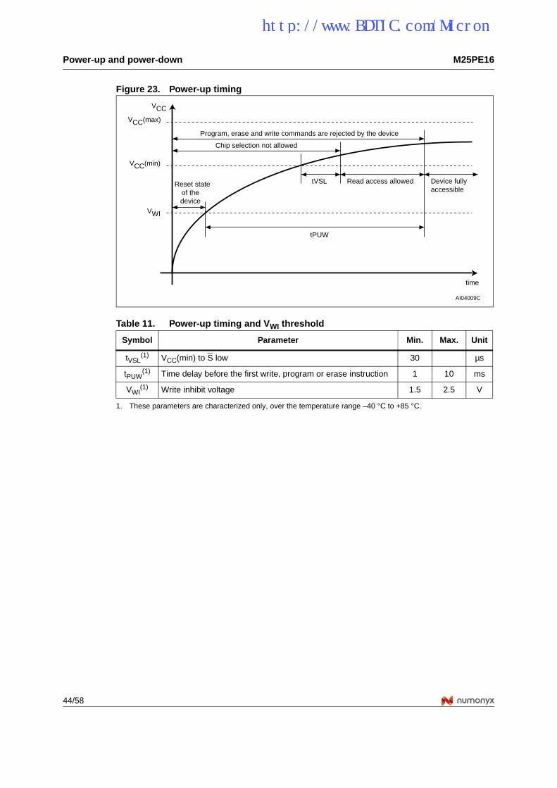
Power-up and power-down M25PE16
44/58
Figure 23. Power-up timing
Table 11. Power-up timing and VWI threshold
Symbol Parameter Min. Max. Unit
tVSL(1)
1. These parameters are characterized only, over the temperature range –40 °C to +85 °C.
VCC(min) to S low 30 µs
tPUW(1) Time delay before the first write, program or erase instruction 1 10 ms
VWI(1) Write inhibit voltage 1.5 2.5 V
VCC
AI04009C
VCC(min)
VWI
Reset stateof thedevice
Chip selection not allowed
Program, erase and write commands are rejected by the device
tVSL
tPUW
time
Read access allowed Device fullyaccessible
VCC(max)
http://www.BDTIC.com/Micron
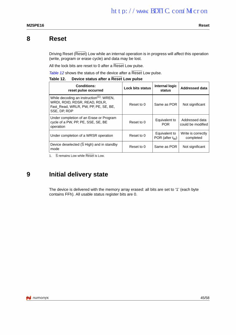
M25PE16 Reset
45/58
8 Reset
Driving Reset (Reset) Low while an internal operation is in progress will affect this operation (write, program or erase cycle) and data may be lost.
All the lock bits are reset to 0 after a Reset Low pulse.
Table 12 shows the status of the device after a Reset Low pulse.
9 Initial delivery state
The device is delivered with the memory array erased: all bits are set to ‘1’ (each byte contains FFh). All usable status register bits are 0.
Table 12. Device status after a Reset Low pulse
Conditions: reset pulse occurred
Lock bits statusInternal logic
statusAddressed data
While decoding an instruction(1): WREN, WRDI, RDID, RDSR, READ, RDLR, Fast_Read, WRLR, PW, PP, PE, SE, BE, SSE, DP, RDP
1. S remains Low while Reset is Low.
Reset to 0 Same as POR Not significant
Under completion of an Erase or Program cycle of a PW, PP, PE, SSE, SE, BE operation
Reset to 0Equivalent to
PORAddressed data
could be modified
Under completion of a WRSR operation Reset to 0Equivalent to
POR (after tW)Write is correctly
completed
Device deselected (S High) and in standby mode
Reset to 0 Same as POR Not significant
http://www.BDTIC.com/Micron
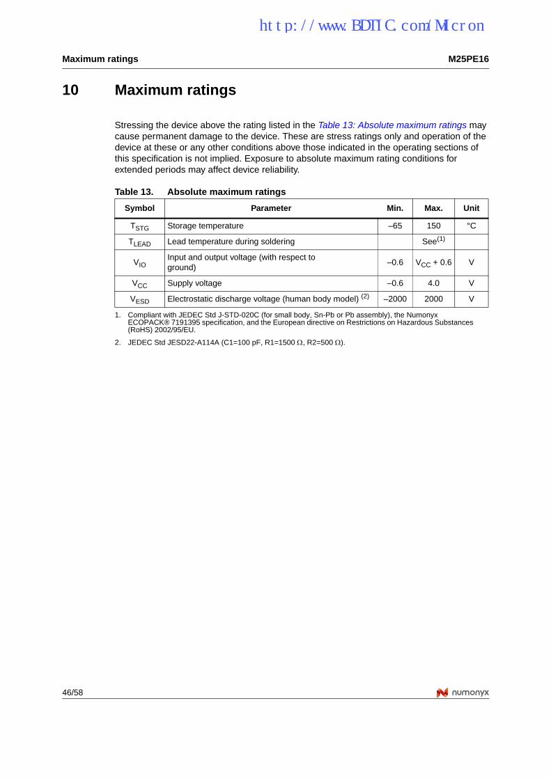
Maximum ratings M25PE16
46/58
10 Maximum ratings
Stressing the device above the rating listed in the Table 13: Absolute maximum ratings may cause permanent damage to the device. These are stress ratings only and operation of the device at these or any other conditions above those indicated in the operating sections of this specification is not implied. Exposure to absolute maximum rating conditions for extended periods may affect device reliability.
Table 13. Absolute maximum ratings
Symbol Parameter Min. Max. Unit
TSTG Storage temperature –65 150 °C
TLEAD Lead temperature during soldering See(1)
1. Compliant with JEDEC Std J-STD-020C (for small body, Sn-Pb or Pb assembly), the Numonyx ECOPACK® 7191395 specification, and the European directive on Restrictions on Hazardous Substances (RoHS) 2002/95/EU.
VIOInput and output voltage (with respect to ground)
–0.6 VCC + 0.6 V
VCC Supply voltage –0.6 4.0 V
VESD Electrostatic discharge voltage (human body model) (2)
2. JEDEC Std JESD22-A114A (C1=100 pF, R1=1500 Ω, R2=500 Ω).
–2000 2000 V
http://www.BDTIC.com/Micron
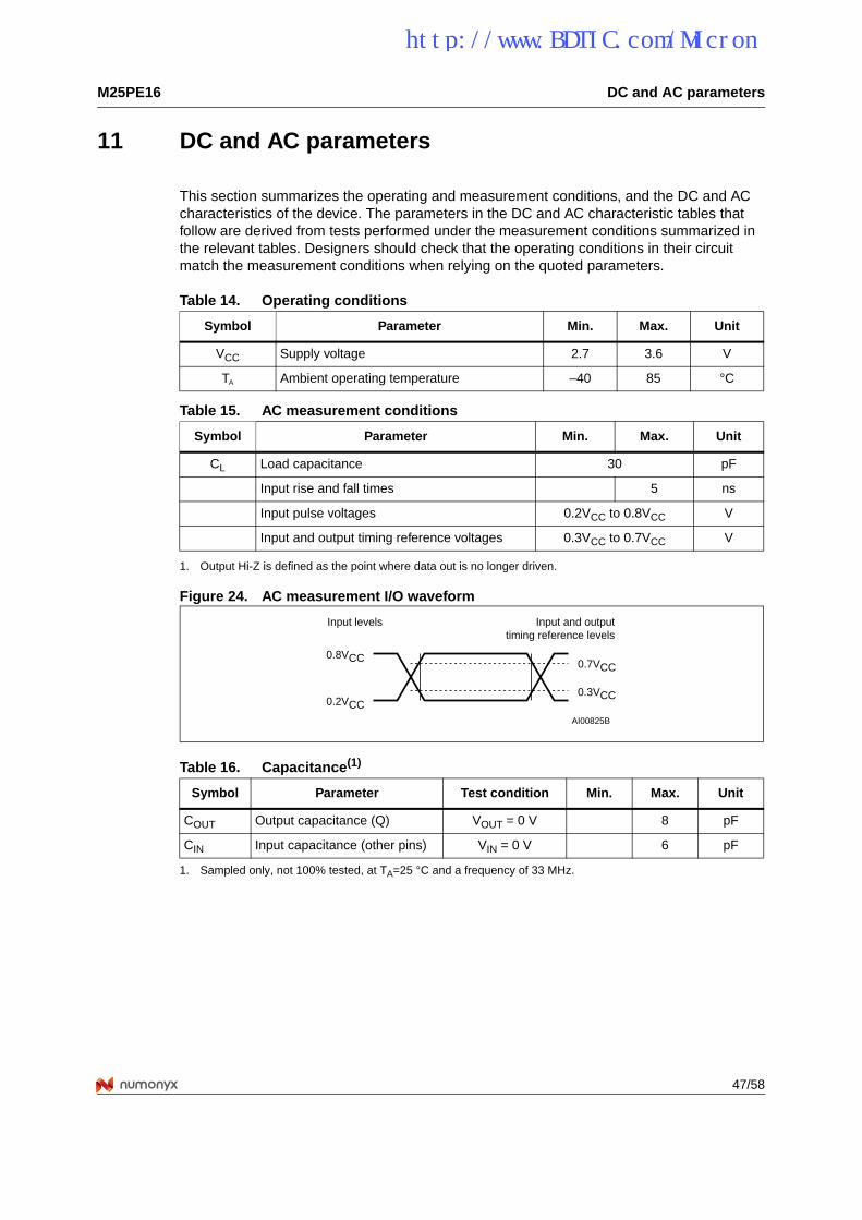
M25PE16 DC and AC parameters
47/58
11 DC and AC parameters
This section summarizes the operating and measurement conditions, and the DC and AC characteristics of the device. The parameters in the DC and AC characteristic tables that follow are derived from tests performed under the measurement conditions summarized in the relevant tables. Designers should check that the operating conditions in their circuit match the measurement conditions when relying on the quoted parameters.
1. Output Hi-Z is defined as the point where data out is no longer driven.
Figure 24. AC measurement I/O waveform
Table 14. Operating conditions
Symbol Parameter Min. Max. Unit
VCC Supply voltage 2.7 3.6 V
TA Ambient operating temperature –40 85 °C
Table 15. AC measurement conditions
Symbol Parameter Min. Max. Unit
CL Load capacitance 30 pF
Input rise and fall times 5 ns
Input pulse voltages 0.2VCC to 0.8VCC V
Input and output timing reference voltages 0.3VCC to 0.7VCC V
Table 16. Capacitance(1)
1. Sampled only, not 100% tested, at TA=25 °C and a frequency of 33 MHz.
Symbol Parameter Test condition Min. Max. Unit
COUT Output capacitance (Q) VOUT = 0 V 8 pF
CIN Input capacitance (other pins) VIN = 0 V 6 pF
AI00825B
0.8VCC
0.2VCC
0.7VCC
0.3VCC
Input and outputtiming reference levels
Input levels
http://www.BDTIC.com/Micron
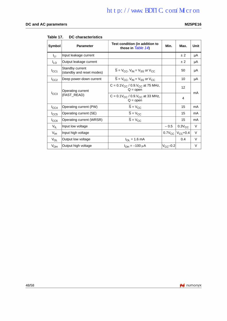
DC and AC parameters M25PE16
48/58
Table 17. DC characteristics
Symbol ParameterTest condition (in addition to
those in Table 14)Min. Max. Unit
ILI Input leakage current ± 2 µA
ILO Output leakage current ± 2 µA
ICC1Standby current(standby and reset modes)
S = VCC, VIN = VSS or VCC 50 µA
ICC2 Deep power-down current S = VCC, VIN = VSS or VCC 10 µA
ICC3Operating current (FAST_READ)
C = 0.1VCC / 0.9.VCC at 75 MHz,Q = open
12
mAC = 0.1VCC / 0.9.VCC at 33 MHz,
Q = open4
ICC4 Operating current (PW) S = VCC 15 mA
ICC5 Operating current (SE) S = VCC 15 mA
ICC6 Operating current (WRSR) S = VCC 15 mA
VIL Input low voltage – 0.5 0.3VCC V
VIH Input high voltage 0.7VCC VCC+0.4 V
VOL Output low voltage IOL = 1.6 mA 0.4 V
VOH Output high voltage IOH = –100 µA VCC–0.2 V
http://www.BDTIC.com/Micron
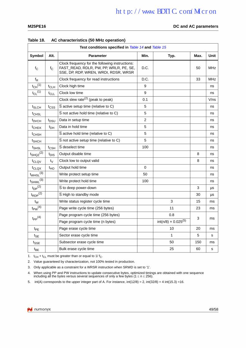
M25PE16 DC and AC parameters
49/58
Table 18. AC characteristics (50 MHz operation)
Test conditions specified in Table 14 and Table 15
Symbol Alt. Parameter Min. Typ. Max. Unit
fC fC
Clock frequency for the following instructions: FAST_READ, RDLR, PW, PP, WRLR, PE, SE, SSE, DP, RDP, WREN, WRDI, RDSR, WRSR
D.C. 50 MHz
fR Clock frequency for read instructions D.C. 33 MHz
tCH(1) tCLH Clock high time 9 ns
tCL(1) tCLL Clock low time 9 ns
Clock slew rate(2) (peak to peak) 0.1 V/ns
tSLCH tCSS S active setup time (relative to C) 5 ns
tCHSL S not active hold time (relative to C) 5 ns
tDVCH tDSU Data in setup time 2 ns
tCHDX tDH Data in hold time 5 ns
tCHSH S active hold time (relative to C) 5 ns
tSHCH S not active setup time (relative to C) 5 ns
tSHSL tCSH S deselect time 100 ns
tSHQZ(2) tDIS Output disable time 8 ns
tCLQV tV Clock low to output valid 8 ns
tCLQX tHO Output hold time 0 ns
tWHSL(3) Write protect setup time 50 ns
tSHWL(3) Write protect hold time 100 ns
tDP(2) S to deep power-down 3 µs
tRDP(2) S High to standby mode 30 µs
tW Write status register cycle time 3 15 ms
tPW(4) Page write cycle time (256 bytes) 11 23 ms
tPP(4)
Page program cycle time (256 bytes) 0.83 ms
Page program cycle time (n bytes) int(n/8) × 0.025(5)
tPE Page erase cycle time 10 20 ms
tSE Sector erase cycle time 1 5 s
tSSE Subsector erase cycle time 50 150 ms
tBE Bulk erase cycle time 25 60 s
1. tCH + tCL must be greater than or equal to 1/ fC.
2. Value guaranteed by characterization, not 100% tested in production.
3. Only applicable as a constraint for a WRSR instruction when SRWD is set to ‘1’.
4. When using PP and PW instructions to update consecutive bytes, optimized timings are obtained with one sequence including all the bytes versus several sequences of only a few bytes (1 ≤ n ≤ 256).
5. int(A) corresponds to the upper integer part of A. For instance, int(12/8) = 2, int(32/8) = 4 int(15.3) =16.
http://www.BDTIC.com/Micron
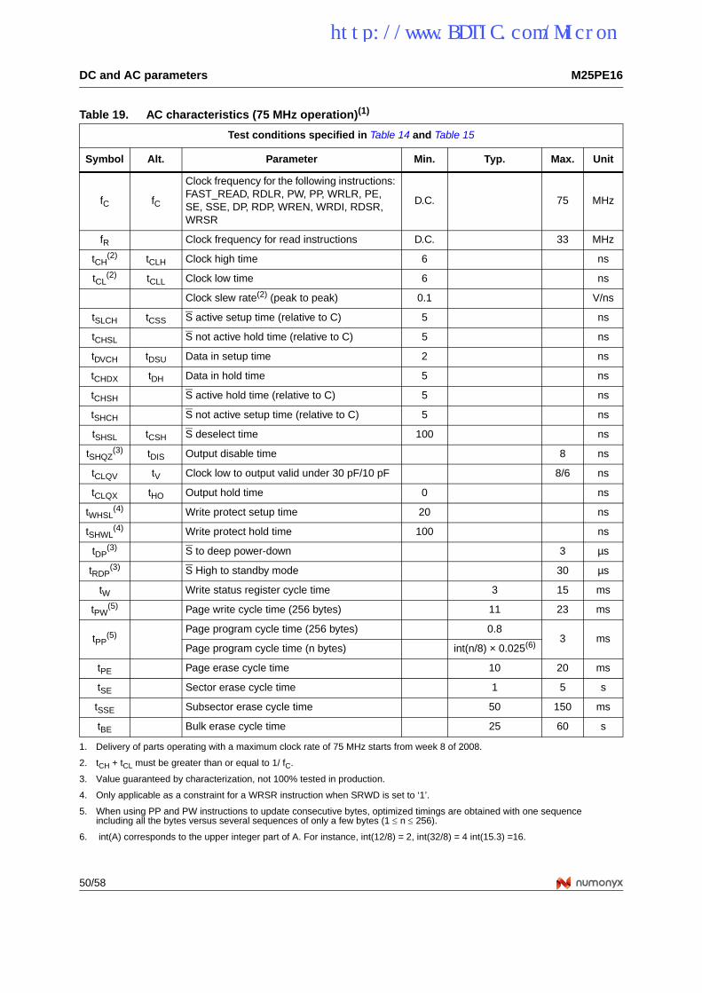
DC and AC parameters M25PE16
50/58
Table 19. AC characteristics (75 MHz operation)(1)
Test conditions specified in Table 14 and Table 15
Symbol Alt. Parameter Min. Typ. Max. Unit
fC fC
Clock frequency for the following instructions: FAST_READ, RDLR, PW, PP, WRLR, PE, SE, SSE, DP, RDP, WREN, WRDI, RDSR, WRSR
D.C. 75 MHz
fR Clock frequency for read instructions D.C. 33 MHz
tCH(2) tCLH Clock high time 6 ns
tCL(2) tCLL Clock low time 6 ns
Clock slew rate(2) (peak to peak) 0.1 V/ns
tSLCH tCSS S active setup time (relative to C) 5 ns
tCHSL S not active hold time (relative to C) 5 ns
tDVCH tDSU Data in setup time 2 ns
tCHDX tDH Data in hold time 5 ns
tCHSH S active hold time (relative to C) 5 ns
tSHCH S not active setup time (relative to C) 5 ns
tSHSL tCSH S deselect time 100 ns
tSHQZ(3) tDIS Output disable time 8 ns
tCLQV tV Clock low to output valid under 30 pF/10 pF 8/6 ns
tCLQX tHO Output hold time 0 ns
tWHSL(4) Write protect setup time 20 ns
tSHWL(4) Write protect hold time 100 ns
tDP(3) S to deep power-down 3 µs
tRDP(3) S High to standby mode 30 µs
tW Write status register cycle time 3 15 ms
tPW(5) Page write cycle time (256 bytes) 11 23 ms
tPP(5)
Page program cycle time (256 bytes) 0.83 ms
Page program cycle time (n bytes) int(n/8) × 0.025(6)
tPE Page erase cycle time 10 20 ms
tSE Sector erase cycle time 1 5 s
tSSE Subsector erase cycle time 50 150 ms
tBE Bulk erase cycle time 25 60 s
1. Delivery of parts operating with a maximum clock rate of 75 MHz starts from week 8 of 2008.
2. tCH + tCL must be greater than or equal to 1/ fC.
3. Value guaranteed by characterization, not 100% tested in production.
4. Only applicable as a constraint for a WRSR instruction when SRWD is set to ‘1’.
5. When using PP and PW instructions to update consecutive bytes, optimized timings are obtained with one sequence including all the bytes versus several sequences of only a few bytes (1 ≤ n ≤ 256).
6. int(A) corresponds to the upper integer part of A. For instance, int(12/8) = 2, int(32/8) = 4 int(15.3) =16.
http://www.BDTIC.com/Micron
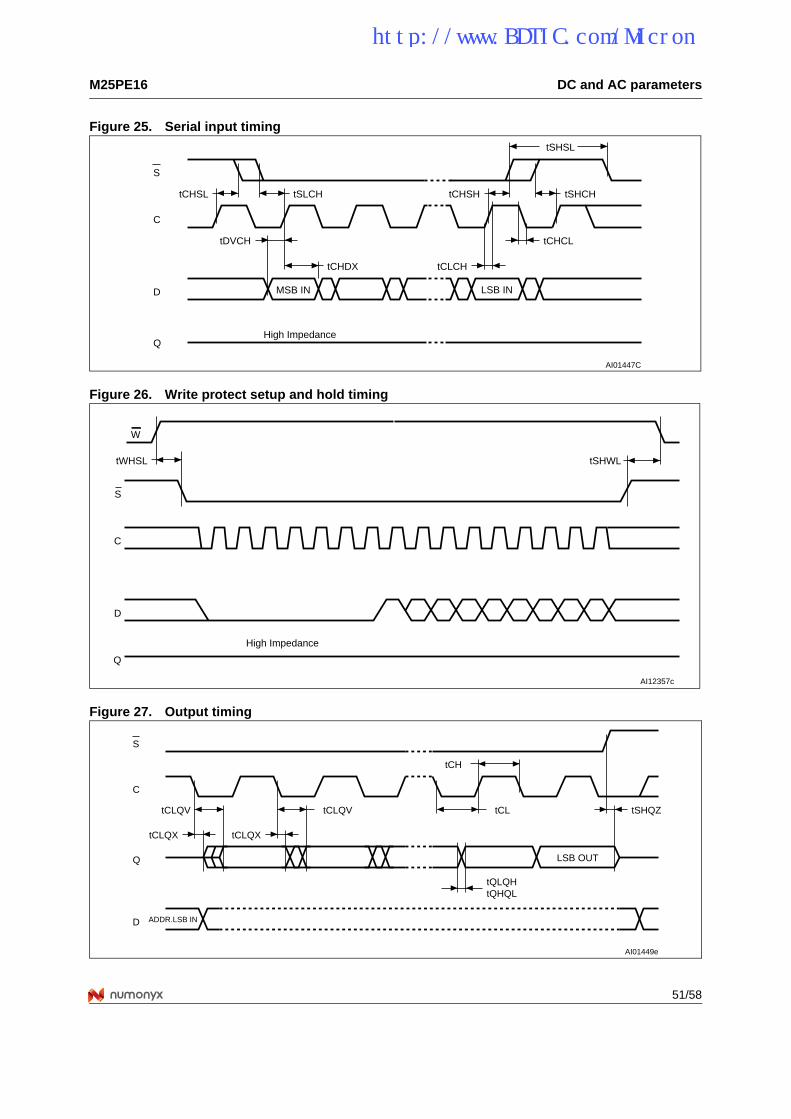
M25PE16 DC and AC parameters
51/58
Figure 25. Serial input timing
Figure 26. Write protect setup and hold timing
Figure 27. Output timing
C
D
AI01447C
S
MSB IN
Q
tDVCH
High Impedance
LSB IN
tSLCH
tCHDX
tCHCL
tCLCH
tSHCH
tSHSL
tCHSHtCHSL
C
D
S
Q
High Impedance
W
tWHSL tSHWL
AI12357c
C
Q
AI01449e
S
LSB OUT
D ADDR.LSB IN
tSHQZ
tCH
tCL
tQLQHtQHQL
tCLQX
tCLQV
tCLQX
tCLQV
http://www.BDTIC.com/Micron
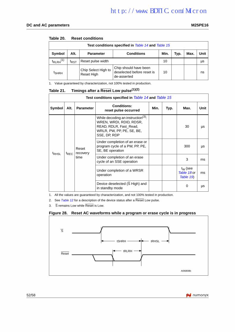
DC and AC parameters M25PE16
52/58
Figure 28. Reset AC waveforms while a program or erase cycle is in progress
Table 20. Reset conditions
Test conditions specified in Table 14 and Table 15
Symbol Alt. Parameter Conditions Min. Typ. Max. Unit
tRLRH(1)
1. Value guaranteed by characterization, not 100% tested in production.
tRST Reset pulse width 10 µs
tSHRHChip Select High to Reset High
Chip should have been deselected before reset is de-asserted
10 ns
Table 21. Timings after a Reset Low pulse(1)(2)
1. All the values are guaranteed by characterization, and not 100% tested in production.
2. See Table 12 for a description of the device status after a Reset Low pulse.
Test conditions specified in Table 14 and Table 15
Symbol Alt. ParameterConditions:
reset pulse occurred Min. Typ. Max. Unit
tRHSL tREC
Reset recovery time
While decoding an instruction(3): WREN, WRDI, RDID, RDSR, READ, RDLR, Fast_Read, WRLR, PW, PP, PE, SE, BE, SSE, DP, RDP
3. S remains Low while Reset is Low.
30 µs
Under completion of an erase or program cycle of a PW, PP, PE, SE, BE operation
300 µs
Under completion of an erase cycle of an SSE operation
3 ms
Under completion of a WRSR operation
tW (see Table 18 or Table 19)
ms
Device deselected (S High) and in standby mode
0 µs
AI06808b
ResettRLRH
S
tRHSLtSHRH
http://www.BDTIC.com/Micron
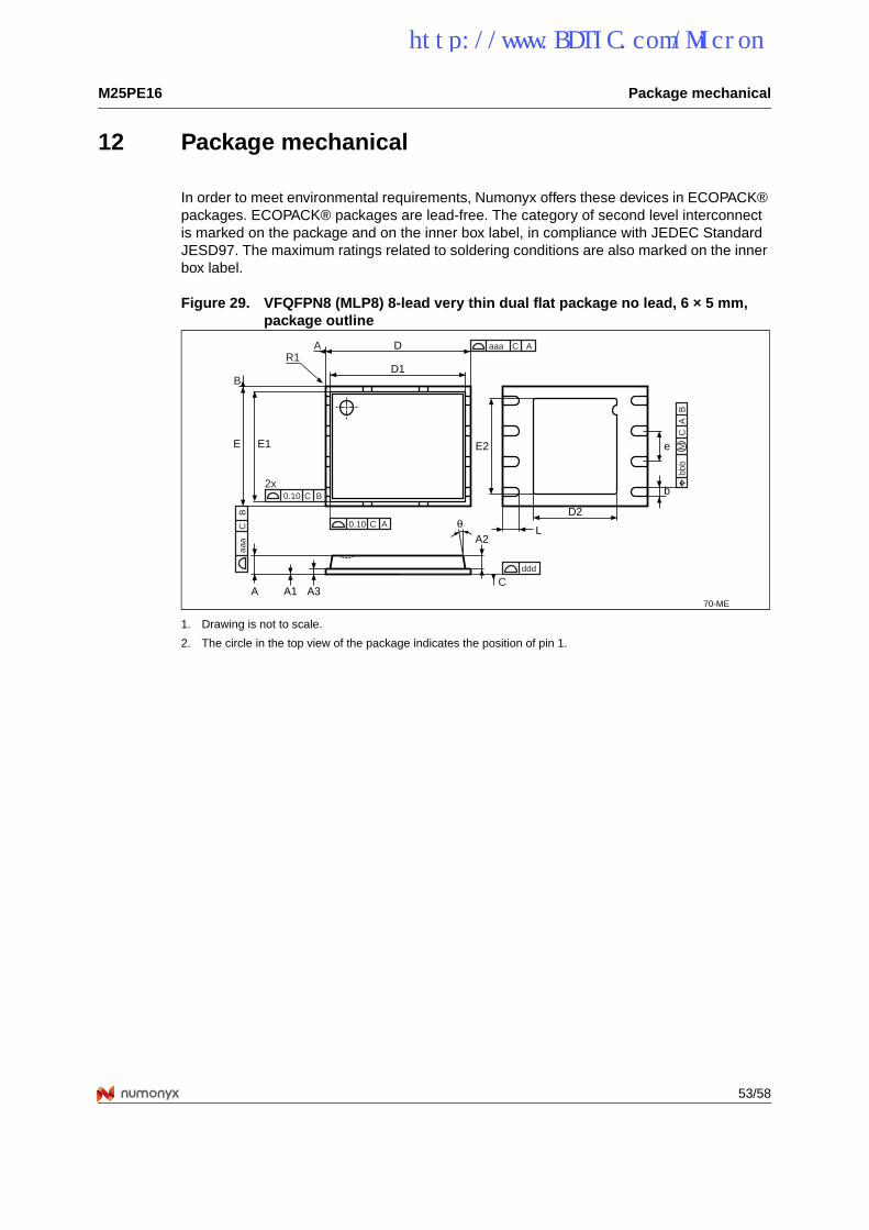
M25PE16 Package mechanical
53/58
12 Package mechanical
In order to meet environmental requirements, Numonyx offers these devices in ECOPACK® packages. ECOPACK® packages are lead-free. The category of second level interconnect is marked on the package and on the inner box label, in compliance with JEDEC Standard JESD97. The maximum ratings related to soldering conditions are also marked on the inner box label.
Figure 29. VFQFPN8 (MLP8) 8-lead very thin dual flat package no lead, 6 × 5 mm,package outline
1. Drawing is not to scale.
2. The circle in the top view of the package indicates the position of pin 1.
D
E
70-ME
A2
A A3A1
E1
D1
eE2
D2
L
b
θ
R1
ddd
bbb
C
CA
B
aaa C AA
B
aaa
CB
M
0.10 C A
0.10 C B2x
http://www.BDTIC.com/Micron
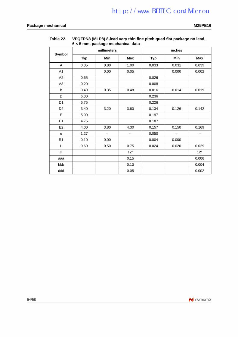
Package mechanical M25PE16
54/58
Table 22. VFQFPN8 (MLP8) 8-lead very thin fine pitch quad flat package no lead,6 × 5 mm, package mechanical data
Symbolmillimeters inches
Typ Min Max Typ Min Max
A 0.85 0.80 1.00 0.033 0.031 0.039
A1 0.00 0.05 0.000 0.002
A2 0.65 0.026
A3 0.20 0.008
b 0.40 0.35 0.48 0.016 0.014 0.019
D 6.00 0.236
D1 5.75 0.226
D2 3.40 3.20 3.60 0.134 0.126 0.142
E 5.00 0.197
E1 4.75 0.187
E2 4.00 3.80 4.30 0.157 0.150 0.169
e 1.27 – – 0.050 – –
R1 0.10 0.00 0.004 0.000
L 0.60 0.50 0.75 0.024 0.020 0.029
Θ 12° 12°
aaa 0.15 0.006
bbb 0.10 0.004
ddd 0.05 0.002
http://www.BDTIC.com/Micron
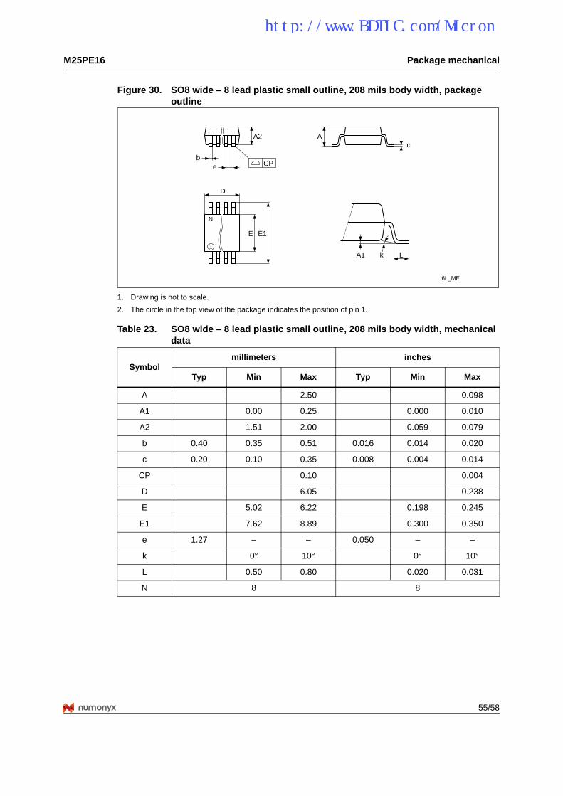
M25PE16 Package mechanical
55/58
Figure 30. SO8 wide – 8 lead plastic small outline, 208 mils body width, package outline
1. Drawing is not to scale.
2. The circle in the top view of the package indicates the position of pin 1.
Table 23. SO8 wide – 8 lead plastic small outline, 208 mils body width, mechanical data
Symbolmillimeters inches
Typ Min Max Typ Min Max
A 2.50 0.098
A1 0.00 0.25 0.000 0.010
A2 1.51 2.00 0.059 0.079
b 0.40 0.35 0.51 0.016 0.014 0.020
c 0.20 0.10 0.35 0.008 0.004 0.014
CP 0.10 0.004
D 6.05 0.238
E 5.02 6.22 0.198 0.245
E1 7.62 8.89 0.300 0.350
e 1.27 – – 0.050 – –
k 0° 10° 0° 10°
L 0.50 0.80 0.020 0.031
N 8 8
6L_ME
E
N
CPb
e
A2
D
c
LA1 k
E1
A
1
http://www.BDTIC.com/Micron
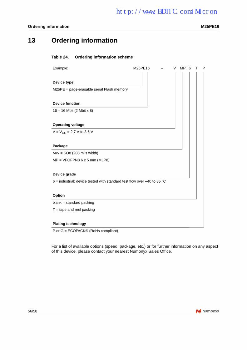
Ordering information M25PE16
56/58
13 Ordering information
For a list of available options (speed, package, etc.) or for further information on any aspect of this device, please contact your nearest Numonyx Sales Office.
Table 24. Ordering information scheme
Example: M25PE16 – V MP 6 T P
Device type
M25PE = page-erasable serial Flash memory
Device function
16 = 16 Mbit (2 Mbit x 8)
Operating voltage
V = VCC = 2.7 V to 3.6 V
Package
MW = SO8 (208 mils width)
MP = VFQFPN8 6 x 5 mm (MLP8)
Device grade
6 = industrial: device tested with standard test flow over –40 to 85 °C
Option
blank = standard packing
T = tape and reel packing
Plating technology
P or G = ECOPACK® (RoHs compliant)
http://www.BDTIC.com/Micron
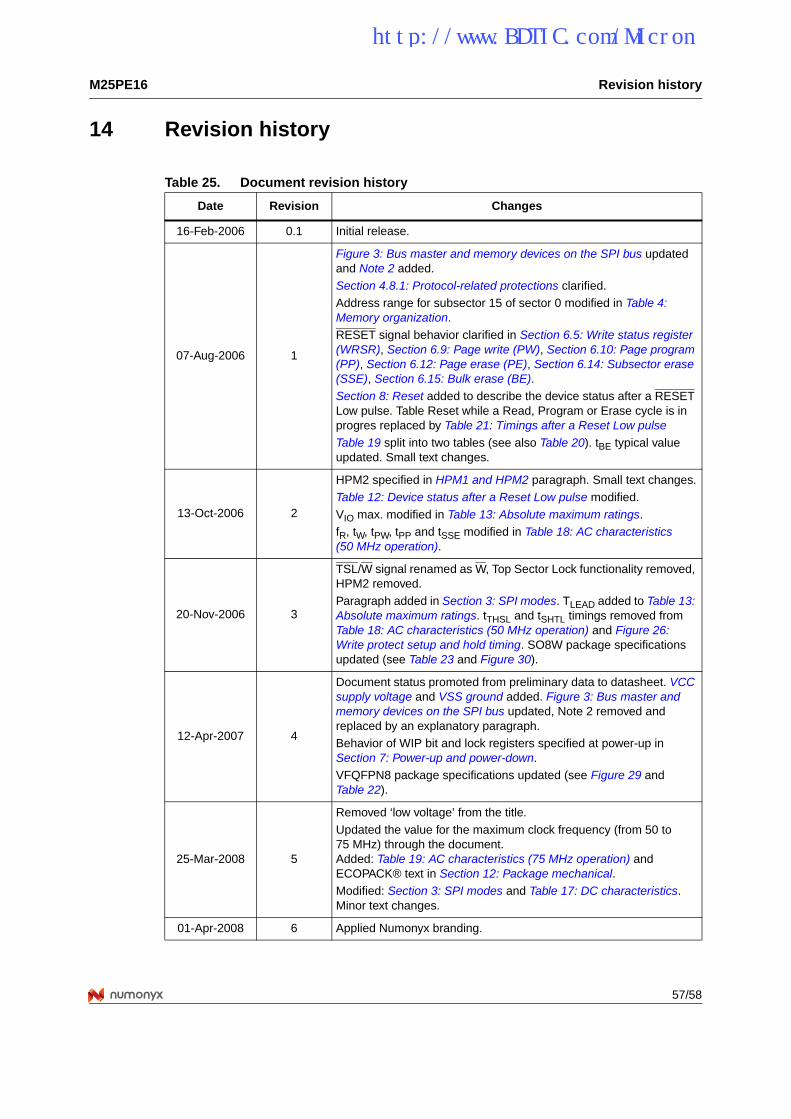
M25PE16 Revision history
57/58
14 Revision history
Table 25. Document revision history
Date Revision Changes
16-Feb-2006 0.1 Initial release.
07-Aug-2006 1
Figure 3: Bus master and memory devices on the SPI bus updated and Note 2 added.
Section 4.8.1: Protocol-related protections clarified.Address range for subsector 15 of sector 0 modified in Table 4: Memory organization.RESET signal behavior clarified in Section 6.5: Write status register (WRSR), Section 6.9: Page write (PW), Section 6.10: Page program (PP), Section 6.12: Page erase (PE), Section 6.14: Subsector erase (SSE), Section 6.15: Bulk erase (BE).
Section 8: Reset added to describe the device status after a RESET Low pulse. Table Reset while a Read, Program or Erase cycle is in progres replaced by Table 21: Timings after a Reset Low pulse
Table 19 split into two tables (see also Table 20). tBE typical value updated. Small text changes.
13-Oct-2006 2
HPM2 specified in HPM1 and HPM2 paragraph. Small text changes.
Table 12: Device status after a Reset Low pulse modified.
VIO max. modified in Table 13: Absolute maximum ratings.fR, tW, tPW, tPP and tSSE modified in Table 18: AC characteristics (50 MHz operation).
20-Nov-2006 3
TSL/W signal renamed as W, Top Sector Lock functionality removed, HPM2 removed.
Paragraph added in Section 3: SPI modes. TLEAD added to Table 13: Absolute maximum ratings. tTHSL and tSHTL timings removed from Table 18: AC characteristics (50 MHz operation) and Figure 26: Write protect setup and hold timing. SO8W package specifications updated (see Table 23 and Figure 30).
12-Apr-2007 4
Document status promoted from preliminary data to datasheet. VCC supply voltage and VSS ground added. Figure 3: Bus master and memory devices on the SPI bus updated, Note 2 removed and replaced by an explanatory paragraph.Behavior of WIP bit and lock registers specified at power-up in Section 7: Power-up and power-down.VFQFPN8 package specifications updated (see Figure 29 and Table 22).
25-Mar-2008 5
Removed ‘low voltage’ from the title.
Updated the value for the maximum clock frequency (from 50 to 75 MHz) through the document.Added: Table 19: AC characteristics (75 MHz operation) and ECOPACK® text in Section 12: Package mechanical.Modified: Section 3: SPI modes and Table 17: DC characteristics.Minor text changes.
01-Apr-2008 6 Applied Numonyx branding.
http://www.BDTIC.com/Micron
M25PE16
58/58
Please Read Carefully:
INFORMATION IN THIS DOCUMENT IS PROVIDED IN CONNECTION WITH NUMONYX™ PRODUCTS. NO LICENSE, EXPRESS OR IMPLIED, BY ESTOPPEL OR OTHERWISE, TO ANY INTELLECTUAL PROPERTY RIGHTS IS GRANTED BY THIS DOCUMENT. EXCEPT AS PROVIDED IN NUMONYX'S TERMS AND CONDITIONS OF SALE FOR SUCH PRODUCTS, NUMONYX ASSUMES NO LIABILITY
WHATSOEVER, AND NUMONYX DISCLAIMS ANY EXPRESS OR IMPLIED WARRANTY, RELATING TO SALE AND/OR USE OF NUMONYX PRODUCTS INCLUDING LIABILITY OR WARRANTIES RELATING TO FITNESS FOR A PARTICULAR PURPOSE, MERCHANTABILITY, OR INFRINGEMENT OF ANY PATENT, COPYRIGHT OR OTHER INTELLECTUAL PROPERTY RIGHT.
Numonyx products are not intended for use in medical, life saving, life sustaining, critical control or safety systems, or in nuclear facility applications.
Numonyx may make changes to specifications and product descriptions at any time, without notice.
Numonyx, B.V. may have patents or pending patent applications, trademarks, copyrights, or other intellectual property rights that relate to the presented subject matter. The furnishing of documents and other materials and information does not provide any license, express or implied,
by estoppel or otherwise, to any such patents, trademarks, copyrights, or other intellectual property rights.
Designers must not rely on the absence or characteristics of any features or instructions marked “reserved” or “undefined.” Numonyx reserves these for future definition and shall have no responsibility whatsoever for conflicts or incompatibilities arising from future changes to them.
Contact your local Numonyx sales office or your distributor to obtain the latest specifications and before placing your product order.
Copies of documents which have an order number and are referenced in this document, or other Numonyx literature may be obtained by visiting Numonyx's website at http://www.numonyx.com.
Numonyx StrataFlash is a trademark or registered trademark of Numonyx or its subsidiaries in the United States and other countries.
*Other names and brands may be claimed as the property of others.
Copyright © 11/5/7, Numonyx, B.V., All Rights Reserved.
http://www.BDTIC.com/Micron