1985-12_hp journal papers
DESCRIPTION
1985-12_HP Journal PapersTRANSCRIPT
H E W L E T T - P A C K A R D CD
LT~L) D E C E M B E R 1 9 8 5
© Copr. 1949-1998 Hewlett-Packard Co.
H E W L E T T - P A C K A R D C D
Lr-ú December 1985 Volume 36 • Number 12
Articles
4 A High-Per t ormance Signa l Generator for RF Communicat ions Test ing, by Rober t E. Burns Cel lu lar radio, FM and TV, and instrument landing systems are among i ts targeted
appl icat ions.
6 User In ter face and In terna l Cont ro l ler for an RF Signal Generator , by A lber t E inste in Lass i ter and Char les R. Kogler The power o f a 68000 microprocessor makes the ins t ru
ment f r iendly , both to the user and to automat ic systems i t may be par t o f .
9 Display Design
10 S i g n a l B u i l t - i n S e r v i c e F e a t u r e s M a x i m i z e U p t i m e , b y M i c h a e l T . W e n d e B u i l t - i n are sel f - tests and service features for faul t locat ion and f ie ld recal ibrat ion.
13 Electr ical ly Erasable PROM Storage for Cal ibrat ion Data
â € ¢ 4 A I n t e r n a l l y M o d u l a r S i g n a l G e n e r a t o r M e c h a n i c a l D e s i g n , b y M i c h a e l B . J e w e l l a n d
field. Mark eas i ly the Each module is l i ke a min i - ins t rument that is eas i ly rep laceab le in the
1O Wide -F requency -Range S igna l Gene ra to r Ou tpu t Sec t i on Des ign , by Robe r t R . Co l - O / /son, James B. Summers , Marv in W. Wagner , and Bryan D. Rat l i f f Output power ampl i f i
cat ion and cont ro l , ampl i tude modulat ion, and reverse power protect ion are handled here.
S i g n a l C . F r e q u e n c y S y n t h e s i z e r D e s i g n , b y T h o m a s R . F a u l k n e r , E a r l C . Her le i kson , Rona ld J . Mayer , B r ian M. M i l l e r , and Mark A . N iemann S ix phase- locked
loops m in im ize phase no ise and spur ious ou tpu ts and p rov ide h igh -accuracy , l ow-d is to r t i on angle modulat ion.
29 Computer Analysis of Osci l la tor Loop Gain, Phase, and Q
31 A u d i o M o d u l a t i o n S e c t i o n f o r a n R F S i g n a l G e n e r a t o r , b y G a r y L T o n g I n c l u d e d i s a low-distor t ion, var iable-modulat ion audio s ignal source.
36 1985 Index
4 3 A u t h o r s
Editor, Richard Susan Dolan • Associate Editor, Kenneth A Shaw • Assistant Editor, Nancy R-Teater • Art Director, Photographer, Arvid A. Danielson • Support Supervisor, Susan E.Wright Il lustrator, Publisher, S. Vanderbloom, • Administrative Services, Typography, Anne S. LoPresti • European Production Supervisor, Michael Zandwi|ken • Publisher, Russell M H. Berg
2 HEWLETT-PACKARD JOURNAL DECEMBER 1985 e> Hewlett-Packard Company 1985 Printed in U S.A.
© Copr. 1949-1998 Hewlett-Packard Co.
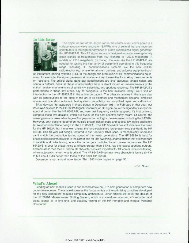
In this Issue The object on top of the acry l ic rod in the center of our cover photo is a
surface-acoust ic-wave resonator (SAWR), one of several that are important contr ibutors to the high performance of a new synthesized signal generator, the HP 8642A B. This RF signal source is designed to produce exceptional ly c lean s igna ls a t f requenc ies f rom 100 k i l ohe r t z to 1057 .5 megaher t z (A mode l ) a re 2115 megaher tz (B mode l ) . Sources l i ke the HP 8642AB a re needed for test ing the vast array of equipment operat ing in th is f requency r a n g e , i n c l u d i n g R F c o m m u n i c a t i o n s s y s t e m s l i k e t h e n e w c e l l u l a r radiotelephones, home entertainment devices, and avionics equipment such
as instrument landing systems ( ILS). In the design and product ion of RF communicat ions equip ment, making example, the signal generator simulates an ideal transmitter for making measurements on rece ivers . The cr i t ica l s igna l generator spec i f icat ions are leve l accuracy, phase no ise, and s p u r i o u s t h e b e c a u s e t h e s e c h a r a c t e r i s t i c s h a v e a d i r e c t i m p a c t o n m e a s u r e m e n t s o f t h e crit ical receiver characteristics of sensit ivity, selectivity, and spurious response. The HP 8642A/B's per fo rmance in these key a reas , say i t s des igners , i s the bes t ava i lab le today . You ' l l f i nd an introduct ion to the HP 8642A/B in the ar t ic le on page 4. The other s ix ar t ic les in th is issue deal wi th and contr ibut ions to the state of the ar t in i ts e lectr ical and mechanical designs, s impl i f ied control calibration. operation, automatic test system compatibility, and simplified repair and calibration.
SAW dev ices f i rs t appeared in these pages in December 1981. In February o f that year , our issue designed devoted to the HP 8662A Signal Generator, an RF signal source designed for exceptional spec t ra l to l i ke the HP 8642A/B , and ve ry fas t f requency sw i t ch ing speed . I t ' s i ns t ruc t i ve to compare the two des igns , wh ich a re r i va ls fo r the bes t -spec t ra l -pur i t y award . Of course , the newer development, takes advantage of five years of technological development, including the SAWRs. However, both designs depend on mult ip le phase- locked loops and special low-noise osci l lators (a swi tched- inductance des ign in the HP 8662A) . The HP 8642A/B doesn ' t e l iminate the need for the standard, 8662A, but it may well unseat the long-established low-phase-noise standard, the HP 8640B. This 13-year-old design, featured in our February 1973 issue, is mechanical ly tuned and c a n ' t H P t h e p r o d u c t i o n t e s t i n g s p e e d o f t h e n e w e r g e n e r a t o r s . T h e H P 8 6 6 2 A i s b e s t f o r phase noise closer than 5 kHz to the carrier and for fast switching, characteristics that are important in satel l i te and radar test ing, where the carr ier gets mult ipl ied to microwave frequencies. The HP 8642A/B outputs, best for phase noise at offsets greater than 5 kHz, has the lowest spurious outputs, and costs testing, than the HP 8662A. Its characteristics are important for RF communications testing, where adjacent channel noise is crit ical. The HP 8642A/B's phase noise characterist ics are similar to but about 6 dB bet ter than those of the o lder HP 8640B.
December is our annual index issue. The 1985 index begins on page 36.
-P .P . Do lan
What's Ahead Leading off next month's issue is our second art ic le on HP's next generat ion of computers now
under development. The art icle discusses the fundamentals of the optimizing compilers developed for the new computers ' reduced-complex i ty archi tecture. Other ar t ic les wi l l cover the design of the HP recorder, Measurement Plott ing System, which is a waveform recorder, X-Y recorder, and d ig i ta l p lo t te r a l l i n one un i t , and usab i l i t y tes t i ng o f t he HP Por tab le and In teg ra l Pe rsona l Computers.
DECEMBER 1985 HEWLETT-PACKARD JOURNALS
© Copr. 1949-1998 Hewlett-Packard Co.
A High-Performance Signal Generator for RF Communicat ions Test ing High-re l iabi l i ty design, extended cal ibrat ion intervals, and fast ca l ibrat ion and repai r maximize ATE system upt ime. Spectral pur i ty is except ional .
by Robert E. Burns
AS THE COMMUNICATIONS SPECTRUM becomes increasingly crowded, requirements for the equip ment used in communications systems become more
stringent. The advent of new methods for people to com municate using radio frequencies, such as cellular radio, accelerates this trend. Manufacturers of communications equipment need calibrated signals of high quality to verify that their products are meeting stringent specifications. This needs to be done quickly, usually under computer control. The HP 8642A and 8642B Signal Generators (Fig. 1) can provide these signals.
High-quality communications equipment must transmit and receive voice and other data clearly and accurately over long distances, sometimes in the presence of strong interfer ence at nearby frequencies. To the radio manufacturer, this means that the receiver must be sensitive to very small or weak signals. The noise the receiver adds must be small. The receiver must be able to demodulate the data with low distortion. It must also reject all frequencies other than the one it is tuned to.
To test these receiver characteristics, low-noise signals are required whose amplitude and modulation characteris tics can be controlled precisely over a wide dynamic range. The HP 8642A/B can provide signal levels from - 140 dBm (0.023 fj.V) to + 20 dBm (2.24 V) with 0.1-dB resolution and guaranteed accuracy of ±1 dB above 0.1 /u,V over the specified environmental conditions. The frequency range of the HP 8642A is 100 kHz to 1057.5 MHz, and the HP 8642B
generates frequencies from 100 kHz to 2115 MHz. Both mod els have a built-in modulation oscillator that generates sig nals from 20 Hz to 100 kHz. Hence the HP 8642B, with its internal modulation oscillator, can generate frequencies from 20 Hz to 2115 MHz. This represents a dynamic range of eight orders of magnitude for both frequency and ampli tude control. In both models, output can be swept in both fre quency and amplitude. AM can be controlled from 0 to 99.9% with 0.1% resolution. The output signal can be frequency mod ulated to deviations beyond 375 kHz at any carrier frequency (provided that the instantaneous frequency is always above 100 kHz). Phase and pulse modulation are also available.
Perhaps the greatest performance contribution of the HP 8642A/B is its exceptional spectral purity at offsets impor tant in communication systems. The single-sideband (SSB) noise of - 138 dBc/Hz at an offset of 20 kHz from a 1-GHz carrier is further lowered using binary frequency dividers for output frequencies down to 100 kHz, providing excep tionally clean performance throughout the RF spectrum. But low noise is not useful if large spurious signals are present. All HP 8642A/B nonharmonics are guaranteed to be below — 100 dBc. Attention has been paid to other im portant details, such as radiated emissions and third-order intermodulation performance, ensuring exceptional out-of- channel performance. Thus the HP 8642A/B can offer in a fully programmable instrument the level of measurement confidence normally associated only with manually con trolled cavity-tuned generators.
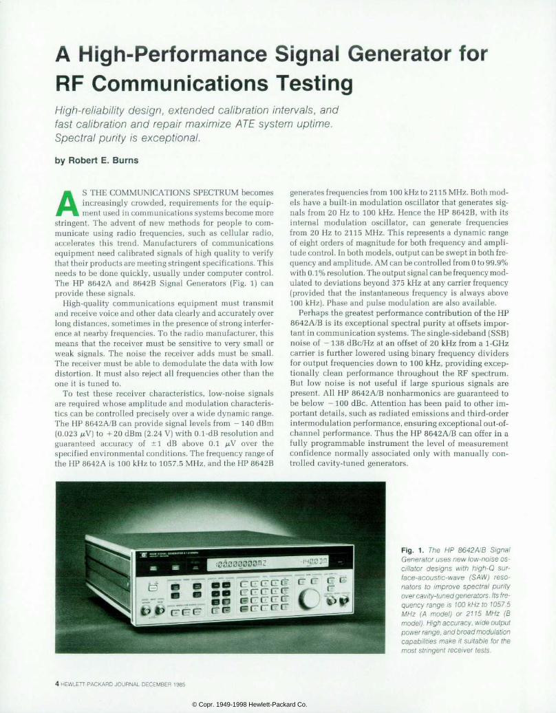
F i g . 1 . T h e H P 8 6 4 2 A / B S i g n a l Generator uses new low-noise os c i l l a t o r d e s i g n s w i t h h i g h - Q s u r f a c e - a c o u s t i c - w a v e ( S A W ) r e s o nators to improve spect ra l pur i ty over cavity-tuned generators. Its fre quency range is 100 kHz to 1057.5 M H z ( A m o d e l ) o r 2 1 1 5 M H z ( B model). High accuracy, wide output power range, and broad modulation capabilit ies make it suitable for the most stringent receiver tests.
4 HEWLETT-PACKARD JOURNAL DECEMBER 1985
© Copr. 1949-1998 Hewlett-Packard Co.
These characteristics allow radio manufacturers to mea sure receiver parameters with high accuracy and confi dence. The signal generator can be tuned to the same fre quency as the receiver to make in-channel measurements such as sensitivity, SINAD (ratio of signal level to noise and distortion), flatness, and distortion. The accurate fre quency, output level, and modulation characteristics of the HP 8642 A/B reduce errors in these measurements. The superior spectral purity of the HP 8642A/B allows accurate measurements of the receiver's ability to reject interference (out-of-channel measurements). In this case, the signal generator is tuned to a frequency different from the fre quency the radio is receiving. The extremely low levels of noise and spurious signals of frequencies other than the HP 8642A/B output frequency means that very little power is generated in the channel the receiver is tuned to. This is important if the receiver's ability to reject interference, or selectivity, is to be measured. These same high-perfor mance characteristics are also useful in general-purpose RF applications.
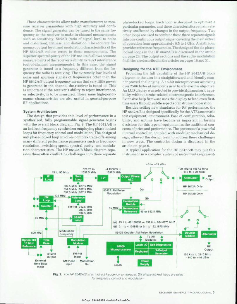
System Architecture The design that provides this level of performance in a
synthesized, fully programmable signal generator begins with the overall block diagram, Fig. 2. The HP 8642A/B is an indirect frequency synthesizer employing phase-locked loops for frequency control and modulation. The design of any phase-locked loop involves complex trade-offs among many different performance parameters such as frequency resolution, switching speed, spectral purity, and modula tion characteristics. The HP 8642A/B block diagram sepa rates these often conflicting challenges into three separate
phase-locked loops. Each loop is designed to optimize a particular parameter, and these characteristics remain rela tively unaffected by changes in the output frequency. Two other loops are used to combine these three separate signals into one continuous output signal covering the main octave of operation from approximately 0.5 to 1 GHz. A sixth loop provides reference frequencies. The design of the six phase- locked loops in the HP 8642A/B is discussed in the article on page 24. The output sections and the audio modulation facilities are described in the articles on pages 1 8 and 3 1 .
Designing for the ATE Environment Providing the full capability of the HP 8642A/B block
diagram to the user in a straightforward and friendly man ner proved challenging. A 16-bit microprocessor accessing over 250K bytes of memory is used to achieve this objective. An LCD display was selected to provide alphanumeric capa bility without strobe-related electromagnetic interference. Extensive help firmware uses the display to lead even first- time users through subtle aspects of instrument operation.
Besides setting new standards for RF performance, the HP 8642A/B is designed specifically for the ATE (automatic test equipment) environment. Ease of configuration, relia bility, and uptime have become as important in buying decisions for this type of equipment as the traditional con cerns of price and performance. The presence of a powerful internal controller, coupled with modular mechanical de sign, allowed the design team to address these challenges in new ways. The controller design is discussed in the article on page 6.
A typical application for the HP 8642A/B may put this instrument in a complex system of instruments represent-
+ 5 t o + 2 1 d B m
45 to 90 MHz 528.75 to
1057.5 MHz 4.130859 to 1057.5 MHz
100kHz to 1057 .5 MHz - 1 4 0 t o + 2 0 d B m
RF Output
Option 001 1 0 M H z
Reference
HP 8642A Only
HP 8642B Only 8642A AM/Pulse
Modulation
45.1 to 49.130859 or 832.6 to 964.6875 MHZ 0.1 to 4 .130859 or 0 .1 to 132.1875 MHz
Modulation Frequency 8642B Doubler AM Pulse Modulat ion 500 kHz
External T ime Base
Input
FM/PM Input
A M P u l s e M o d u l a t i o n I n p u t O u t
RF Output
100 kHz to 2115 MHz - 1 4 0 t o + 1 6 d B m
HP-IB
Fig. phase-locked are HP 8642 A/B is an indirect frequency synthesizer. Six phase-locked loops are used for f requency contro l and modulat ion.
DECEMBER 1985 HEWLETT-PACKARD JOURNAL 5
© Copr. 1949-1998 Hewlett-Packard Co.
ing large investments in equipment and engineering. High uptime, the percentage of time the instrument is not down for troubleshooting, repair, or calibration, is important for the user to benefit fully from the investment made in a complex test system. High uptime starts with good reliabil ity. During development of the HP 8642A/B, this meant extensive stress analysis of all components, junction tem peratures analyzed and minimized, and copious amounts of air flow provided. Development hardware at every phase was subjected to extensive stress testing involving thermal, mechanical, and electrical shock.
Given a collection of over 3000 electrical components, however, the likelihood of failure can be minimized but will still remain finite. Clearly there are advantages to going beyond designing for reliability and considering the design impacts on diagnostics, troubleshooting, and repair. Key to easy serviceability is a mechanical product design that allows easy access to critical circuitry. This objective is usually at odds with the packaging requirements of a syn thesizer having a - 100 dBc specification on spurious out puts, where often the first impulse is to weld it shut. In the HP 8642A/B, a clamshell die-cast housing maximizes the grounding area available for low-pressure gasketing. This, coupled with the rigidity of the die-cast housings, minimizes the number of fasteners required to seal a mod ule. All RF circuitry is housed in one of eight die-cast modules. These modules have well-defined specifications on all inputs and outputs. They can be individually ex tended quickly and easily by releasing two snap fasteners. By removing typically six to eight screws, large sections of critical circuitry can be exposed and analyzed while operating. Details of the mechanical design are in the article on page 14.
This sort of accessibility is only valuable if a fault can be quickly traced to an individual module. To achieve this goal, basic test equipment such as a voltmeter and a power meter are built into the instrument. Each module contains an analog multiplexer that allows access to several critical monitoring points, yet adds only one filtered line to the module. These points are polled and monitored through several different levels of diagnostic tests. Critical failures, such as loop unlock, are monitored continuously. Exten
sive diagnostic firmware allows the operator to trace most faults to the module level without removing the instrument covers. If maximum system uptime is a must, a failed mod ule can simply be exchanged with a new module in min utes. An EAROM sent with the new module can be down loaded into instrument memory quickly and easily, bring ing the instrument into calibration without the need for any manual adjustments. If component-level repair is more appropriate, the built-in diagnostics can help track down the faulty component. If it becomes necessary to replace a critical component, the HP 8642A/B can recalibrate itself automatically. Acting as an HP-IB controller, it can direct certain pieces of associated test equipment to make mea surements, then store the new calibration data internally. Using these features, engineers were able to trace induced faults in developmental HP 8642A/Bs over the telephone using modems.
The serviceability approach taken for the HP 8642A/B is discussed in the article on page 10. Built upon a foundation of high reliability, these diagnostic and serviceability fea tures should contribute to saved time and money for design ers of RF test systems.
Acknowledgments Many people contributed to the HP 8642A/B project over
a number of years, making it impossible to mention all of the key people here. Fundamental to the development of this product were the design engineers who are represented as authors in following articles. Also worthy of mention are the contributions of Tim Carey, Fred Ivés, and Roger Muat to the original block diagram design. Rob Oeflein and John Richardson helped refine the product concept. Early design decisions benefitted from inputs from Steve Hold- away and Mike Hadley . Eric Anderson and Jon Sigler achieved the amazing feat of maintaining unyielding positions on product reliability and serviceability without creating enemies. Efforts well beyond the call of duty were turned in by Morris Chase, technician, and Billy Reynolds, tooling engineer. And finally, the entire group was orchestrated through the critical phases by Art Upham, program man ager extraordinaire.
User Interface and Internal Controller for an RF Signal Generator b y A l b e r t E i n s t e i n L a s s i t e r a n d C h a r l e s R . K o g l e r
THE USER INTERFACE of the HP 8642A/B Signal Generator is designed to provide many conveniences and to make the instrument easy to use. The user
interface includes the keyboard, the display, and the HP-IB
(IEEE 488) interface. The HP 8642A/B has a 25-character alphanumeric dis
play for function settings and messages (see box, page 9). The instrument prompts the user with what is expected
6 HEWLETT-PACKARD JOURNAL DECEMBER 1985
© Copr. 1949-1998 Hewlett-Packard Co.
next in many cases so the operating manual doesn't have to be depended upon so heavily. Messages tell the user what is going on or what the user has done wrong. For example, AM TURNED OFF is displayed if AM is on when pulse modulation is selected. This message helps the user learn that AM can't be done simultaneously with pulse modulation. Another example is AMPTD LIMITS MAX AM. which tells the user that the requested AM setting is not allowed at the current amplitude setting.
Two user-defined displayable messages can be used for any desired purpose. These messages allow the display to be used as a test system's large-character display for prompting the operator, or for recording a company's cap ital asset number for the instrument inside the instrument, or for any other user-defined message. These user-defined battery-backed-up messages can be kept and displayed on demand, or output over the HP-IB.
All individual indicators outside the display have been eliminated by using the alphanumeric display. Individual indicators like SHIFT, RF.OFF, and PULSE simply appear in the alphanumeric display, thereby reducing the cost and clutter of the front panel. By using the alphanumeric dis play and by using individual LCD sigments as one-word indi cators, about 40 individual indicators were eliminated.
A pull-out card is sometimes provided in other instru ments to supply lists of message codes, HP-IB codes, and special functions. The need for a pull-out card has been eliminated by using the alphanumeric display and by print ing HP-IB codes for all keys on the front panel near each key. The list of special functions is scrolled through on the display using the HELP function; since all messages are alphanumeric, there is no need to list the special functions on a pull-out card.
HP 8642A/B messages have a message code at the right end of each message (for example, E24 in the message AMPTD LIMITS MAX AM .E24). This message code allows easy refer ence to the operating manual, where each message is de scribed more thoroughly. These descriptions are useful to those unfamiliar with the full meaning of messages and the abbreviations used within messages, and could be espe cially useful for nonEnglish-speaking users. Most of the descriptions of messages include a statement of what caused the message and what to do about it.
Built- in Convenience The OFF ON key is used to toggle functions off and on.
This key reduces the number of keys and the number of individual indicators needed for functions, and presents to the user a consistent, easy-to-understand method for turning functions off and on. This key is also used to recover from errors caused by accidentally hitting the wrong keys. Functions can be turned back on easily to their last selected values.
Amplitude can be set directly in units of dBm, volts, mV, fj,V, and dBjuV. It can be set in other units, like dBV, dBmV, dBf, and dB relative to an arbitrary amplitude set ting, by using the amplitude relative capabilities of the HP 8642A/B. The HP 8642A/B can also convert amplitude set tings to any other amplitude units. For customers working in EMF amplitude units (popular in Europe and Japan) the HP 8642A/B has an EMF mode that causes all amplitude
settings to be displayed and entered in EMF amplitude units (like EMF V. dB EMF ¿A', and so on). Once the amplitude units are configured, the user only needs to press one amplitude units key to terminate a new amplitude setting.
The knob functions on the HP 8642 A B are designed to provide conveniences to the user in setting functions. The knob can be used with any of the instrument's function settings, for manual sweeps, for scrolling through the list of special functions using the HELP function, or for changing the phase of the RF output in 1° steps. Each function also has its own settable increment value, which can be used with the STEP o and STEP o keys, or with the knob during the KNOB INCR mode. For instrument settings, when the knob is turned quickly, larger steps are taken, so the setting changes much more quickly. The knob algorithm allows the user to have control over three and sometimes four digits without having to change the knob resolution. This algorithm allows the user to go all the way from the minimum setting to the maximum and back in a relatively small number of turns. Once near a desired setting, turning the knob slowly gives precise steps of single digits to fine- tune the setting. The KNOB INCR mode allows the customer to define the size of each step. This mode can be used for putting (frequency) channel spacings on the knob so that each step from the knob gives the next channel. The KNOB HOLD function allows the knob to be dedicated to one func tion, while any other function is changed with the STEP keys and the DATA keypad. This function can be used to change frequency with the knob while changing amplitude with the STEP keys. The KNOB HOLD function can greatly re duce keystrokes when changing two parameters interactively.
The HP 8642A/B has 51 nonvolatile save/recall registers, which save all instrument settings, special functions, knob resolution, and other data. The recall registers can be used to make complicated instrument setups quickly and easily, to select the user's favorite modes (like EMF units, FM preemphasis, etc.), or just to make automatic testing work more quickly (RECALL is faster than setting states over the HP-IB). SAVE and RECALL can be used with the STEP o- and STEP o keys to set up or modify sequences of recall regis ters, or to recall the last state recalled before the instru ment's state was modified. The SEQuence function steps through instrument setups saved in consecutive recall re gisters. This function is especially useful in semiautomatic systems; an operator can sequence through up to 51 differ ent states while testing or adjusting another unit under test.
HP-IB Design The nonvolatile HP-IB address is settable from the front
panel. To keep the instrument usable in a system even if the battery is dead, an internal switch will be read at turn-on if the address is lost.
The HP-IB status byte is designed so that it cari be used flexibly during either status polling or when a service re quest (SRQ) causes an interrupt to a program. Of particular interest is how the HP 8642A/B communicates messages to the HP-IB controller. Three groups of messages are inter nally kept track of for possible HP-IB output. Parameter changed messages inform the user that the HP 8642A/B has changed some other setting to allow a new setting.
DECEMBER 1985 HEWLETT-PACKARD JOURNAL 7
© Copr. 1949-1998 Hewlett-Packard Co.
Execution error messages describe the HP 8642A/B's reason for not executing an attempted setting. Hardware error mes sages signal the presence of an internal hardware problem that the user might be able to resolve. There are separate status bits and message lists, and separate functions to clear the status bits and read back the messages for each of these three groups of messages. This separation provides enough flexibility to allow the HP-IB user to decide what types of messages to handle or ignore and when to handle them. For example, the user may want to ignore parameter changed messages, handle execution error messages by polling the status byte, and handle hardware error messages by having SRQ cause an interrupt.
Messages can be output as message code numbers (for easy comparison by a computer) or as alphanumeric strings (for message handling by a human or for output to a printer) . The ability to output messages as alphanumeric strings can eliminate the need to look up message code numbers when developing a program.
The settings of functions are easily read over the HP-IB using the output active function (OA) command. The setting is output as a string that includes the function prefix and units. This string can be read directly into a numeric vari able on an HP-IB computer or it can be read into a string variable which can be later written back to the HP 8642A/B to get that setting again. The string can be used to print the instrument's settings on a printer. As a convenience to users of a particular set of amplitude units, amplitude set tings are output in whatever units they are set in (e.g., dB EMF /xV or dB relative to the amplitude reference). The display can be read over the HP-IB, including cursor posi tions and the state of the display indicators below the al phanumeric characters. By reading the display, the states of modulation sources, special functions, increment set values, references, and so on can be read via the HP-IB.
The HP-IB interface, combined with the powerful ser vice and diagnostic functions (see article, page 10), results in very powerful, useful, and time-saving capabilities avail able in no other signal generator.
Internal Controller Design Radio frequency (RF) signal generators are primarily
analog instruments, and in the past, their design has been in the analog RF designers' domain. When microprocessors were first used in instruments, their main purpose was automating functions, so the instrument could be used in an automatic test equipment (ATE) environment. The role of the microprocessor has been carried much farther during the development of the HP 8642A/B.
From the very beginning of the project, the analog design ers were encouraged to consider the microprocessor an integral part of their design, and to make use of it to the fullest. The digital hardware/firmware team demonstrated its commitment to this philosophy by selecting a 16-bit 68000 instead of a less powerful 8-bit microprocessor. The implementation of this design philosophy has resulted in a very high degree of microprocessor interaction with the analog hardware, and provides the customer higher perfor mance, better reliability, and more functionality for lower cost.
The digital hardware/firmware design team had several
key goals. Maximum performance and functionality were needed. The internal controller had to provide what was needed for the instrument's modules to meet their particu lar input and output specifications. The complicated set of signal generator hardware and capabilities had to be presented in a friendly, easy-to-use manner.
Extensive serviceability-related built-in features such as module swap, self-calibration, and self-diagnostics were to be implemented to maximize the uptime of the instrument and to reduce costs during production (see article, page 10).
The power of the microprocessor made possible a wide range of easy-to-use functions that provide additional use ful instrument capabilities. These capabilities are im plemented totally or mostly in firmware, using hardware that is already required to perform some other function. For example, stepped frequency sweep, phase-continous frequency sweep, and amplitude sweep are implemented in firmware. The only hardware added for these sweeps is a DAC (digital-to-analog converter) for the X-axis output, an output line for the Z-axis output, and one extra control line for the IF reference loop. Special functions to set fre quency to 0.1-Hz resolution, to change the output phase in one-degree steps, to invert the polarity of the external FM/PM input, to disable settling (for faster switching), and to hold the attenuator setting during amplitude setting changes are implemented with no additional hardware. The RF OFF/ON function (which reduces the RF level with out switching the attenuators, thereby prolonging at tenuator life) requires no additional hardware, because it uses a combination of filter and divider switching and re duction of the output section vernier level. The dcFM up date mode special function (which shows frequency drift on the display during dcFM) uses hardware already re quired for doing dcFM correction.
The HP 8642A/B hardware is rather complicated, with many instances of coupled functions. That is, the range of one function's settings may be limited by the settings of other functions. Range checking of functions is optimized to allow the user to get the maximum performance and flexibility from the instrument. An example of this flexibil ity is the coupling between the amplitude and AM settings. At amplitudes above 14 dBm, it is not possible to get the maximum AM depth of 99.9%. The combination of amplitude and AM settings is limited such that the output is limited to a maximum peak envelope power of 20 dBm. Thus, at an amplitude setting of 15.8 dBm, the user is allowed to set AM as high as 62.2%. Conversely, if the user has AM set to 30%, the instrument allows the amplitude to be set up to 17.7 dBm. More complicated examples of coupled functions are the relationship between RF fre quency, FM, modulation frequency, and the FM preem- phasis special function, and the relationship between center frequency, sweep span, and sweep time for phase- continuous frequency sweep. Again in these cases, the user is allowed the maximum possible performance for all com binations of the coupled functions.
The microprocessor controls and reads over 300 bits of instrument hardware information. Of these, about 250 bits relate to analog hardware control and feedback. The proces sor is especially interactive with the modulation oscillator. Normally, the microprocessor counts the modulation fre-
8 HEWLETT-PACKARD JOURNAL DECEMBER 1985
© Copr. 1949-1998 Hewlett-Packard Co.
quency and feeds back correction data to the oscillator hardware. This processor interaction enables the instru ment to meet its stringent specifications for modulation oscillator accuracy without resorting to a synthesized mod ulation source and associated spurious outputs. This cor rection process can take up to 250 ms. For faster tuning speed, a special function that disables this counting and correcting for each modulation oscillator change can be used. Correction data from the previous counting and cor recting cycle is used instead. Since the amount of drift over time is relatively small, the user can calibrate the settings when a test begins by using the count and correct algorithm (or the user can use a different special function that calib
rates all five modulation oscillator bands at once) for the first setting(s) of the modulation oscillator, then switch to the other algorithm with negligible loss of accuracy, but with much faster switching time.
Heavy processor interaction with analog hardware is also used during dcFM (see article, page 24).
Acknowledgments Mike Wende also worked on the design of the controller
hardware. We would like to thank Art Upham for numerous and invaluable contributions. Lynn Wheelwright supplied and supported our firmware development tools. Morris Chase gave us many valuable suggestions about both
Display Design
In des ign ing the HP 8642A/B d isp lay , severa l key goa ls had to be met. The instrument state information had to be presented understandably with minimum clutter so that the instrument would be easy to use. The vo lume ava i lab le ins ide the ins t rument for the d isp lay and keyboard was very l im i ted . The d isp lay had to meet mil i tary viewing angle specif ications and had to be viewable in d im in te r I t had to genera te ve ry low e lec t romagne t i c i n te r ference (EMI), and power consumpt ion had to be low. The t rade o f fs c lear ly showed tha t a cus tom a lphanumer ic l i qu id -c rys ta l d isp lay (LCD) was the best way to meet the object ives.
Seven-segment l ight-emitt ing diode (LED) displays were found to d raw too much cur ren t (over an ampere wou ld be needed) . Using that much current would make the power transformer large enough to requ i re the next la rger cab inet s ize . Because o f the s t r i ngen t EMI spec i f i ca t i ons , LEDs cou ld no t be d r i ven mu l t i p lexed to reduce power consumpt ion. Other types o f d isp lays , l i ke CRTs , vacuum f l uo rescen t , and so on , r equ i re t oo much
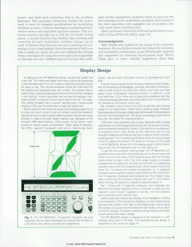
F i g . 1 . T h e H P 8 6 4 2 A / B ' s 1 1 - s e g m e n ! c h a r a c t e r ( a ) a n d charac te r se t (b ) were deve loped to reduce the number o f LCD dr iver pins wi thout resort ing to mult ip lexing.
power , use too much inst rument vo lume, or generate too much EMI.
A l iquid-crystal d isplay al lows the use of alphanumeric charac ters for the display of messages, prompts, and other information, uses a smal l amount o f inst rument vo lume, and uses very l i t t le power LCDs mi l l iamperes inc lud ing dr ivers) . In add i t ion, LCDs cost less than LEDs, there are no a l ignment prob lems wi th the individual display elements, and LCDs allow much more f lexibi l i ty for displaying informat ion to the user.
We needed a way to d r i ve the LCDs to ge t the bes t v iew ing angle for our appl icat ion. LCDs have a v iewing angle l imi ta t ion that depends on the peak voltage applied between the backplane and the individual segments. The larger the voltage used to drive the LCD, the bet ter the v iewing angle is .
LCDs wi th many segments are usual ly designed wi th mul t ip le backplanes so that the segments are actually driven with multiple- level mult iplexed waveforms. When LCDs are driven mult iplexed, of f segments aren' t real ly dr iven at zero vol ts , but only at a low enough voltage so that they do not look turned on within a certain viewing angle. This mult iplexing therefore l imits the drive voltage of the on segments to about 3.2V peak for the type of LCD used in the HP 8642A/B. Below 3.2V the viewing angle is fair ly l imited. Above 3.2V the of f segments star t to look s l ight ly on.
To get the best poss ib le v iewing angle, the HP 8642A/B LCD segments are driven with no mult iplexing, which al lows segments to be dr iven at 5.2V peak (10.4V peak- to-peak) wi th the of f seg men ts d r i ven a t ze ro vo l t s . The 5 .2V power supp ly i s a l ready avai lable for the digital ICs. Driving the LCD with no mult iplexing requires many more LCD segment pins, which means more LCD dr iver ICs. To reduce the number o f segments, an 11 -segment charac ter and charac ter se t a re used ins tead o f the more com mon 14-segment character and character set . This makes i t pos s ib le to dr ive the 25-character d isplay wi th just 1 1 LCD dr ivers (each dr iv ing 32 segments) instead of approximate ly 15.
F ig . 1 shows the 11 -segment cha rac te r and charac te r se t . Note one the center segment of the Z character is real ly just one segment , even though i t appears to be two . The two sec t ions are connected by an internal t race.
Some customers require the display to be readable in a dimly l i t environment. LCDs are passive displays, so they need external l ight ing to be visible in dim l ight. A backl ight ing bar evenly l ights the display using just two incandescent l ight bulbs, one at each end of the display. For better rel iabi l i ty the l ight bulbs are dr iven at wel l below their rated vol tage.
The HP 8642A/B display is designed to be v iewable in a 45° v iew ing cone even in the dark . The back l igh t ing bar des ign i s descr ibed in the ar t ic le on page 14.
DECEMBER 1985 HEWLETT-PACKARD JOURNAL 9
© Copr. 1949-1998 Hewlett-Packard Co.
hardware and firmware related issues. Ken Burden mod ified and helped support our firmware development tools. We would especially like to thank Jena Pittmon and the rest of the technical writing staff for doing such an excellent job in writing the Operating Manual and Operating Funda mentals. These are our best manuals to date and are being used by other divisions as models for how to do instrument manuals. We would like to acknowledge the efforts of the
entire HP 8642A/B production line for bringing problems to our attention promptly and for really taking the quality commitment to heart. We would also like to acknowledge the materials purchasing and scheduling groups and the components engineering group for sustained, high-quality efforts over a long period of time. Finally, thanks to the rest of the HP 8642A/B design team for their efforts in making our job easier.
Signal Generator Service Features Maximize Uptime by Michael T . Wende
TO MAXIMIZE UPTIME, the HP 8642A/B Signal Generator is designed with an emphasis on reliabil ity and extended calibration intervals, so that the
intervals between failures or required calibrations are ex pected to be much longer than in previous generations of HP RF signal generators. To reduce downtime when cali bration or repair does become necessary, the instrument has extensive built-in self-tests and service features for fault detection, fault diagnosis and isolation, and calibration. The fault detection facilities increase measurement confi dence and reduce the time required to locate and fix system problems. The fault diagnosis and isolation facilities quickly isolate problems to one of the HP 8642A/B's inde pendent modules, which can then be replaced easily on-site and recalibrated in minutes without the need for test equip ment. Component-level repair and calibration of individual modules is addressed by other built-in features, including signature analysis, self-calibration routines requiring a minimum of additional equipment, and external automatic calibration capabilities.
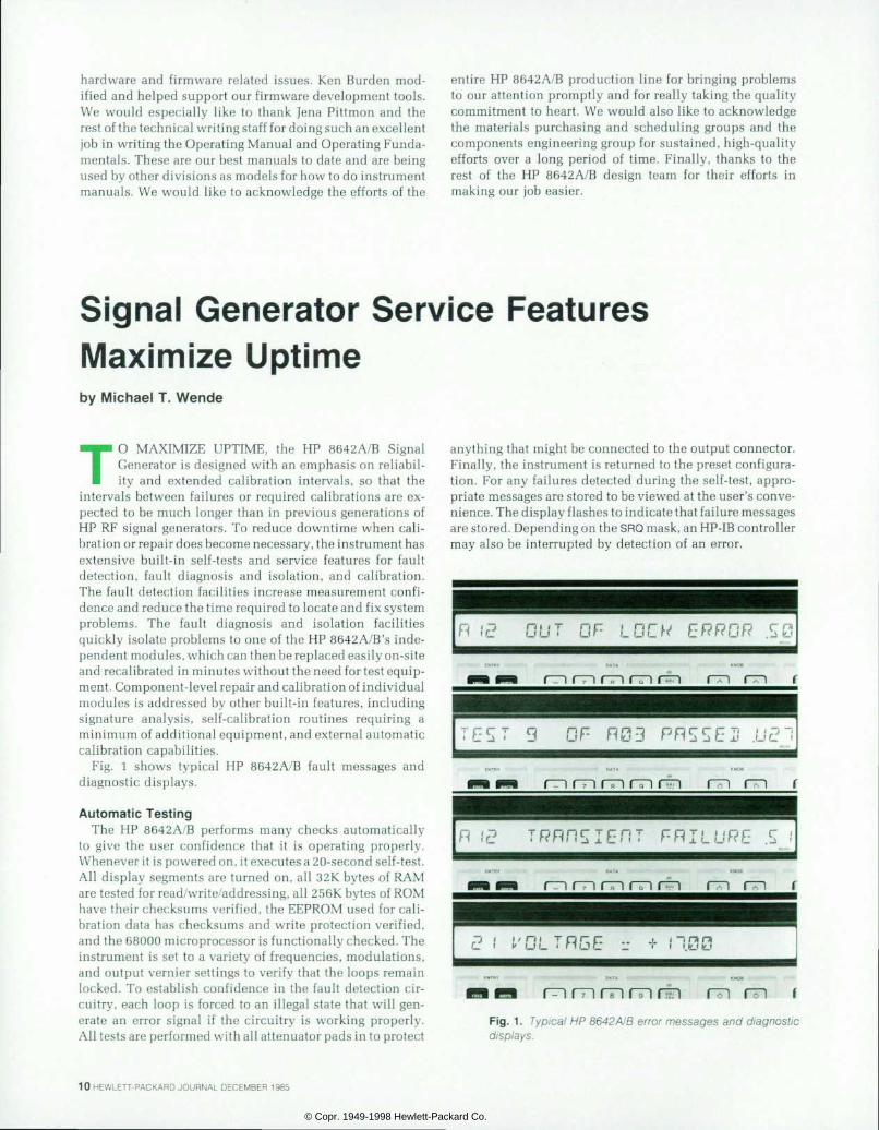
Fig. 1 shows typical HP 8642A/B fault messages and diagnostic displays.
Automatic Test ing The HP 8642A/B performs many checks automatically
to give the user confidence that it is operating properly. Whenever it is powered on, it executes a 20-second self-test. All display segments are turned on, all 32K bytes of RAM are tested for read/write/addressing, all 256K bytes of ROM have their checksums verified, the EEPROM used for cali bration data has checksums and write protection verified, and the 68000 microprocessor is functionally checked. The instrument is set to a variety of frequencies, modulations, and output vernier settings to verify that the loops remain locked. To establish confidence in the fault detection cir cuitry, each loop is forced to an illegal state that will gen erate an error signal if the circuitry is working properly. All tests are performed with all attenuator pads in to protect
anything that might be connected to the output connector. Finally, the instrument is returned to the preset configura tion. For any failures detected during the self-test, appro priate messages are stored to be viewed at the user's conve nience. The display flashes to indicate that failure messages are stored. Depending on the SRQ mask, an HP-IB controller may also be interrupted by detection of an error.
R i c ? O U T O F L O C K E R R O R 5 0
9 O R R 0 3 R R S S E I Ã . U Â ¿ ? ~ Ã
R ! Â ¿ ? T R R R 5 I E R T R R l L L Ã R E 5 !
m f
_ C - i v ( _ ! ( _ ' i I Ã “ C . _ ' ' I . K J K J
m m m m n n m m f Fig. 1 . Typ ica l HP 8642 A/B er ror messages and d iagnost ic displays.
10 HEWLETT-PACKARD JOURNAL DECEMBER 1985
© Copr. 1949-1998 Hewlett-Packard Co.
After the turn-on test, circuitry within the HP 8642A B continuously monitors the phase-locked and ALC loops to trap any errors. The error messages identify whether the specific loop is continuously out of lock (OOL) or had a transient or spurious OOL. The OOL detection circuitry is disabled during switching to avoid misleading messages.
Whenever a user entry occurs, the firmware makes vari ous bounds checks for valid states. Some of the circuits (e.g.. the frequency counter) are tested during state changes. When an instrument state is saved, the battery capacity is checked.
Semiautomatic Diagnost ic Aids Similar to the turn-on test is the instrument-level self-
diagnostic (ILSD). The ILSD requires three to six minutes to run, depending on model and options. This self-test exercises essentially all of the circuits in the entire instru ment. Over 1000 measurements are made at various fre quencies, bands, modulation configurations, and amplitude levels. It is an extremely comprehensive functional test of the HP 8642A/B. While impractical to prove, it is estimated that greater than 80% of all functional failures will be de tected by this collection of subtests. The HP 8642A/B may also be configured as an HP-IB system controller so that an external printer produces a hard copy of the test results. The test may be run in an infinite loop for intermittent failure checking. There is also a stop-on-error mode to pre serve the instrument state for a detected failure. All of this can be controlled from the front panel without any tools or disassembly. In many cases, this test will identify the specific module to be replaced.
Each of the subtests in either the turn-on test or the ILSD can be run separately. There are additional semiautomatic diagnostics that require an operator to move some cables. All of these individual diagnostics are useful either for verifying a failure or for tracing a fault to the component level. All of them may also produce hard-copy results, infinitely loop, and stop on errors like the ILSD.
The turn-on RAM test checks all 32K bytes by reading, inverting, reading, inverting, and reading. This test is non destructive and will catch most failures in RAMs that were previously tested good in the factory. The ILSD contains a more comprehensive RAM diagnostic that conducts a walk ing-ones test. After testing, each RAM section's swapped- out contents are restored. In both tests, if an error is found, the failed RAM chip is identified.
There are various tests to manipulate the display in sev eral ways for checking groups or individual character seg ments and annunciators. Another test prompts the operator to press the keys in a certain order and records any errors.
For the modulation section, one of the semiautomatic diagnostics prompts the operator to connect the unsensed modulation output to the external AM and FM inputs. The built-in routines then manipulate the instrument hardware such that the existing peak detector can be used to check the level out, the audio frequency, and the integrity of the input/output paths.
In the reference summation loop, the built-in diagnostics check several aspects. First, the integrity of the OOL detec tion circuitry must be verified. Each loop may be put into an illegal state that should always generate an OOL signal.
For many, this is accomplished by turning off one of the RF input signals to the loop. The absence of a reference should make any properly working phase-locked loop gen erate an OOL signal. A message is generated if this does not happen. Once the OOL detection circuitry is known to work, the diagnostics will set the instrument to frequencies that require the particular loop under test to lock at the high, middle, and low points of every oscillator band. Lock acqui sition time and power output are checked for each point. Loop lock is also tested with worst-case legal FM modulation on. Both transient and steady-state failures are recorded.
In the output section, because of circuit-to-circuit vari ations in overrange capabilities, some of the diagnostics are adaptive. The algorithm first checks for actual capabil ity above a specified limit, then uses the result for over- modulation testing.
Component-Level Manual Aids Experience with previous instruments has demonstrated
the usefulness of having convenient access to interesting circuit points. The shielding requirements of an instrument such as the HP 8642A/B prohibit the indiscriminate addi tion of connections through the casting walls. Therefore, only one return line is allocated to each module. This line is multiplexed inside the module with several useful circuit nodes and the OOL detection line. The service feedback lines go to the I/O board and are connected in parallel to the OOL latches and an analog multiplexer which selects one line for the voltmeter (Fig. 2).
The internal dc voltmeter consists of a comparator and a 10-bit DAC, which perform a successive approximation under firmware control. A precision voltage reference and ground are measured before the selected point to calibrate the reading. Since some of the sense points are prescaled before being multiplexed, the firmware performs postscal- ing before displaying the reading.
If a more accurate measurement, an ac reading, or an oscilloscope display of a waveform is required, there is a buffered test point on the I/O board where external equip ment may be connected to the built-in multiplexer network. This eliminates much unnecessary mechanical disassem bly during troubleshooting and allows for RF circuit obser vation in situ.
There is also an uncommitted input to the multiplexer network on the I/O board. A user can connect a clip lead to this test point to measure arbitrary circuit nodes. This capability often eliminates the need for additional test equipment.
One of the voltmeter's multiplexer inputs has an RF de tector with response to approximately 1 GHz, along with a coaxial cable. When this point is selected, measured power is displayed in units of dBm. While not accurate enough for calibrating the HP 8642A/B, it is sufficient for troubleshooting the internal RF paths.
Once a problem has been isolated to a relatively small circuit, the technician may need to exercise this circuit in specific ways. Selecting a high-level instrument state (e.g., frequency, amplitude, etc.) corresponding to the desired circuit state requires very detailed knowledge of the instru ment. In the HP 8642A/B, there are many service functions that allow control at many levels. For instance, the fre-
D E C E M B E R 1 9 8 5 H E W L E T T - P A C K A R D J O U R N A L 1 1
© Copr. 1949-1998 Hewlett-Packard Co.
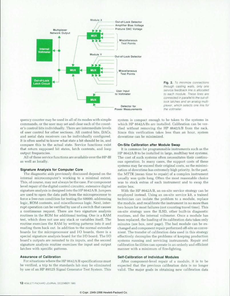
Module X
Multiplexer Network Output
Out-of -Lock Latch Circuit
Out-of-Lock Detector Ampli f ier Bias Voltage Pretune DAC Vol tage
Miscellaneous Test Points
Out-of-Lock Detector
Miscellaneous Test Points
User Input to Voltmeter
Detector for Power Measurements
F ig . 2 . To m in im ize connec t i ons t h r o u g h c a s t i n g w a l l s , o n l y o n e serv ice feedback l ine is a l located to each modu le . These l i nes a re connected in parallel to the out-of- lock la tches and an ana log mu l t i p lexer , which se lects one l ine for the voltmeter.
quency counter may be used in all of its modes with simple commands, or the user may set and clear each of the count er's control bits individually. There are intermediate levels of user control for other sections. All control bits, DACs, and serial data receivers can be individually configured. It is often useful to know what state a bit should be in, and compare this to the actual state. Service functions exist that return supposed bit states, latch contents, and loop output frequencies.
All of these service functions are available over the HP-IB as well as locally.
Signature Analysis for Computer Core The diagnostic aids previously discussed depend on the
internal microcomputer's working to a minimal extent. This, of course, may not always be the case. For component level repair of the digital control circuitry, extensive digital signature analysis is designed into the HP 8642 A/B. Jumpers are used to open the data path from the microprocessor to force a free-run condition for testing the 68000, addressing logic, ROM contents, and miscellaneous logic. Next, inter rupt operation can be verified by use of a switch that causes a continuous request. There are two signature analysis routines in the ROM for additional testing. One is a RAM test, which does not use any stack or variables itself. The routine exercises the RAM by writing patterns into it and reading them back out. In addition to the normal extender boards for the microprocessor and I/O boards, there is a special signature analysis board for the I/O board. The I/O board's outputs are rerouted to its inputs, and the second signature analysis routine exercises the input and output latches with specific patterns.
Assurance of Cal ibrat ion For situations where the HP 8642 A/B specifications must
be verified, a trip to the standards lab may be eliminated by use of an HP 8952S Signal Generator Test System. This
system is compact enough to be taken to the systems in which HP 8642A/Bs are installed. Calibration can be ver ified without removing the HP 8642A/B from the rack. Since this verification takes less than an hour, system downtime can be minimized.
On-Site Cal ibrat ion after Module Swap It is common for programmable instruments such as the
HP 8642A/B to be installed in large, multibay test systems. The cost of such systems often necessitates their continu ous operation. In many cases, the support costs of these systems may far exceed their original costs, so the minimi zation of downtime has extremely high priority. In the past, the MTTR (mean time to repair) of a complex instrument usually was quite long. Often the most reasonable choice was to stock extras of each instrument and to swap the entire box.
With the HP 8642 A/B, an on-site service strategy can be employed instead. Using an on-site service kit, a trained technician can isolate the problem to a module, replace the module, and recalibrate the instrument in no more than two hours for most failures (not counting travel time). This on-site strategy uses the ILSD, other built-in diagnostic routines, and the internal voltmeter. Once a module has been replaced, the loading of its calibration data takes only minutes (see box, next page). The bad module can be ex changed and component repair performed off-site as conve nient. The transfer of calibration data used in this strategy effectively decouples the problems of keeping production systems running and servicing instruments. Repair and calibration facilities can operate in an orderly and efficient manner with a minimum of fire-fighting.
Self-Calibration of Individual Modules After component-level repair of a module, it is to be
expected that the previous calibration data is no longer valid. The major goals in obtaining new calibration data
12 HEWLETT-PACKARD JOURNAL DECEMBER 1985
© Copr. 1949-1998 Hewlett-Packard Co.
are (in order of importance): reliability, minimum set of required equipment, minimum operator training, and minimum operator time. With these goals in mind, the capabilities of the internal computer are exploited. Auto matic calibration routines are built into the HP 8642A B for obtaining the needed data for repaired modules.
These routines have extensive checking built-in to re duce the accidental occurrence of wrong setups or incorrect test equipment. An HP-IB printer can be used to obtain a hard copy of the generated data. Once these routines are executing, the only operator requirement is for an occa sional setup change. The operator is free to attend to other tasks for most of the calibration time. The worst-case equip ment requirements for any of these routines are quite mod est. Depending on the routine selected, an HP 8901A or HP 8901B Modulation Analyzer or an HP 8902 A Measuring Receiver may be needed. Some of the routines require a system DVM that is HP-IB compatible and performs dc and ac voltage measurements. The command set of the DVM is not critical. Miscellaneous cables and adapters are re quired and are provided in the bench service kit. A printer is always optional. No other equipment is required for any of the self-calibration routines.
The reference summation loop is a good example of this built-in self -calibration. For each setup, the HP 8642 A/B first verifies: 1) that the proper internal connections have been made, 2) that the proper connections between the HP 8642A/B and the external test equipment exist, and 3) that the proper external test equipment is on the HP-IB and is correctly configured for the particular set of measurements. Next, the HP 8642A/B hardware is tested to check that it is functioning properly and has the required adjustment ranges. Various loops have multiple oscillator bands, each of which must be separately calibrated. Each band's tuning curve is characterized first. Hundreds of voltage and fre quency measurements are required for this and are au tomatically taken. There is a shaper circuit that corrects the oscillator sensitivity to the desired value. This shaper circuit must also be characterized. For each of the hundreds of calibration points, the pretune and shaper corrections must be individually calculated. This data is then automat ically stored in an EEPROM (see box on the right).
Similiar routines exist for the modulation section, the FM loop, the heterodyne module, and the output section. Some of the modules in the HP 8642A/B do not require such calibration.
External Automatic Calibration The built-in self-calibration does not answer the calibra
tion needs of all situations. There may be occasions where a different set of test equipment is to be used, occasions where a different weighting exists for the calibration goals listed above. For these and other cases, the HP 8642A/B can have its calibration data entered in another way. All of the data can be entered and read out over the HP-IB by any bus controller. With the multiple levels of control avail able through service functions, the circuitry can be manipu lated in the same manner as by the self-calibration routines.
Acknowledgments I would like to acknowledge the help of Rodger Tracy
and Jon Sigler in educating me to our customers' needs and in developing this support strategy. Chris Fames de serves much credit for his day-to-day help and suggestions, as well as for the comprehensive and professional job he did on the support documentation. Morris Chase and Jerry Richardson performed much of the testing and critique of the procedures, hardware, firmware, and documentation. Chuck Kogler implemented a considerable share of the sup port firmware. None of this could have happened without the significant managerial support of Art Upham. I would also like to thank the other members of the R&D team for their cooperation and help where their hardware/firmware was concerned.
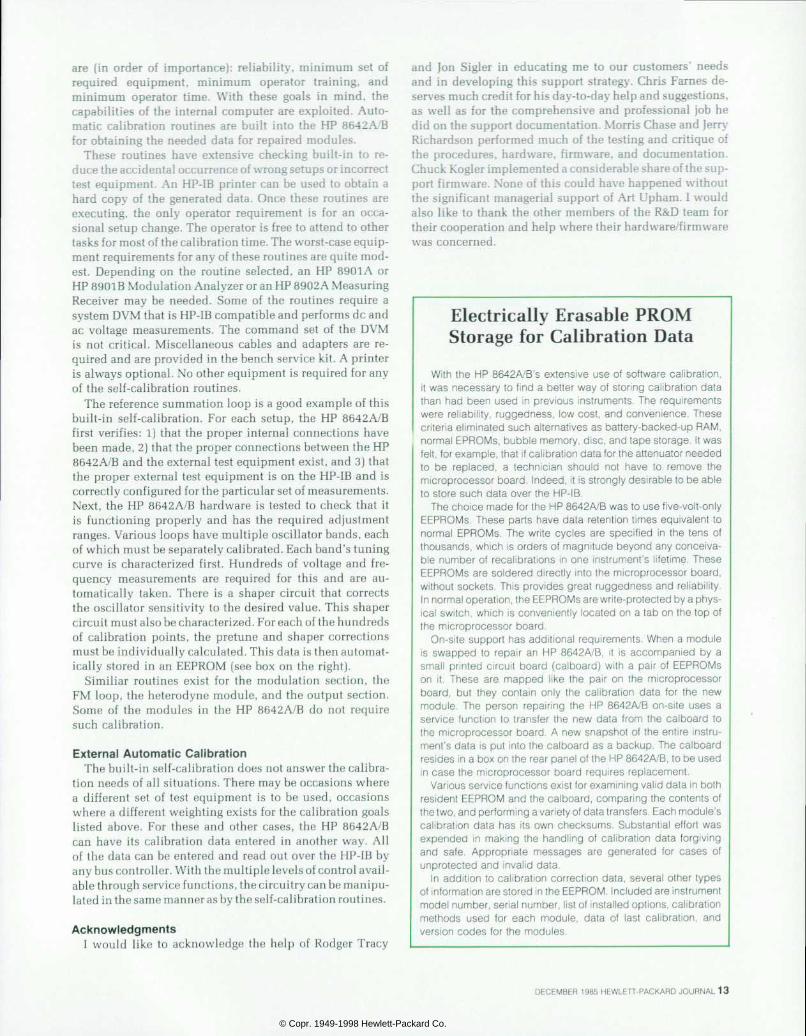
Electrically Erasable PROM Storage for Calibration Data
With the HP 8642A/B's extensive use of sof tware cal ibrat ion, i t was necessary to f ind a bet ter way of s tor ing cal ibrat ion data than had been used in prev ious inst ruments. The requi rements were re l iab i l i ty , ruggedness, low cost , and convenience. These cr i ter ia el iminated such al ternat ives as battery-backed-up RAM. normal EPROMs, bubble memory, disc, and tape storage. I t was felt, needed example, that if calibration data for the attenuator needed t o b e r e p l a c e d , a t e c h n i c i a n s h o u l d n o t h a v e t o r e m o v e t h e microprocessor board. Indeed, i t is strongly desirable to be able to store such data over the HP-IB.
The choice made for the HP 8642A/B was to use f ive-vol t-only EEPROMs. These parts have data retent ion t imes equivalent to normal EPROMs. The wr i te cyc les a re spec i f ied in the tens o f thousands, wh ich is orders o f magni tude beyond any conce iva ble number of recal ibrat ions in one instrument 's l i fe t ime. These EEPROMs are soldered d i rect ly in to the microprocessor board, wi thout sockets. This provides great ruggedness and re l iabi l i ty . In normal operation, the EEPROMs are write-protected by a phys i c a l o f w h i c h i s c o n v e n i e n t l y l o c a t e d o n a t a b o n t h e t o p o f the microprocessor board.
On-s i te suppor t has addi t ional requi rements. When a module i s swapped t o r epa i r an HP 8642A /B , i t i s accompan ied by a smal l p r in ted c i rcu i t board (ca lboard) w i th a pa i r o f EEPROMs on i t . These a re mapped l i ke t he pa i r on t he m ic rop rocesso r boa rd , bu t t hey con ta in on l y t he ca l i b ra t i on da ta f o r t he new modu le . The pe rson repa i r i ng the HP 8642A/B on -s i te uses a serv ice func t ion to t rans fe r the new da ta f rom the ca lboard to the mic roprocessor board . A new snapshot o f the en t i re ins t ru ment 's data is put in to the ca lboard as a backup. The ca lboard resides in a box on the rear panel of the HP 8642A/B, to be used in case the microprocessor board requi res rep lacement .
Various service functions exist for examining val id data in both res ident EEPROM and the ca lboard, compar ing the contents of the two, and performing a variety of data transfers. Each module's ca l ibra t ion data has i ts own checksums. Substant ia l e f for t was expended in mak ing the hand l ing o f ca l ib ra t ion da ta fo rg iv ing a n d s a f e . A p p r o p r i a t e m e s s a g e s a r e g e n e r a t e d f o r c a s e s o f unprotected and inval id data.
In addi t ion to cal ibrat ion correct ion data, several other types of information are stored in the EEPROM. Included are instrument model number, serial number, l ist of instal led options, cal ibrat ion me thods used f o r each modu le , da ta o f l a s t ca l i b ra t i on , and vers ion codes for the modules.
DECEMBER 1985 HEWLETT-PACKARD JOURNAL 13
© Copr. 1949-1998 Hewlett-Packard Co.
Internally Modular Signal Generator Mechanical Design by Michael B. Jewel l and Mark W. Johnson
ONE of the principal goals for the mechanical design of the HP 8642A/B Signal Generator was to provide effective shielding to ensure high performance
without sacrificing serviceability or ease of manufacture. This ruled out "stiff" RF gaskets, large numbers of screws, retaining nuts for RF connectors, and covers that can't be removed without unsoldering components.
The design that realizes these goals divides the circuitry into functional blocks or modules. These modules are treated as small, complete instruments that have well-de fined input and output specifications, require minimum external inputs (power, digital control, and RF signals), and can be completely built and tested before final assem bly, which then requires a minimum of testing and adjust
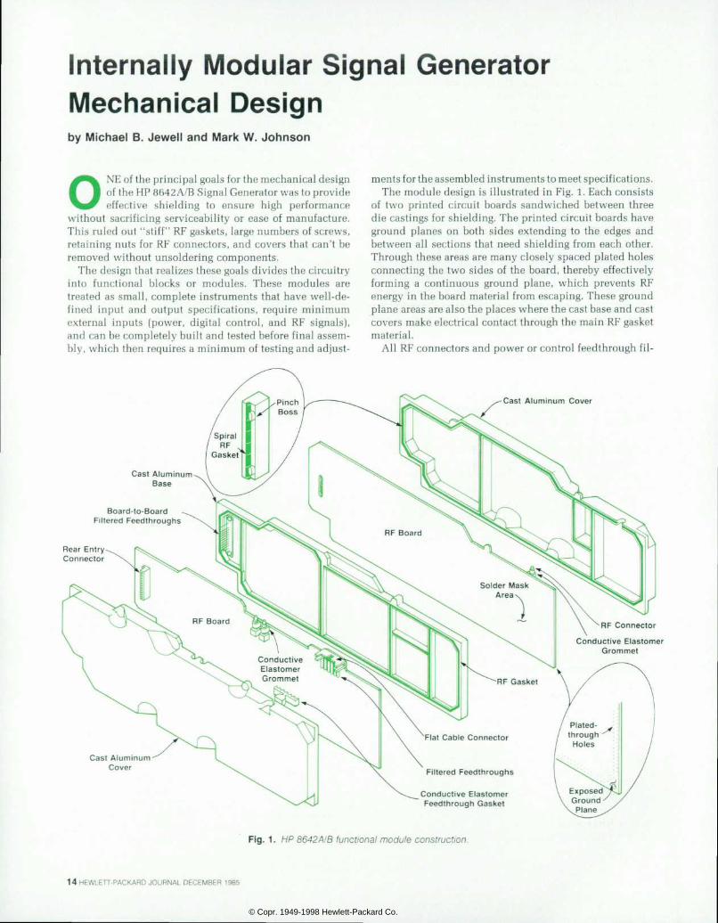
ments for the assembled instruments to meet specifications. The module design is illustrated in Fig. 1. Each consists
of two printed circuit boards sandwiched between three die castings for shielding. The printed circuit boards have ground planes on both sides extending to the edges and between all sections that need shielding from each other. Through these areas are many closely spaced plated holes connecting the two sides of the board, thereby effectively forming a continuous ground plane, which prevents RF energy in the board material from escaping. These ground plane areas are also the places where the cast base and cast covers make electrical contact through the main RF gasket material.
All RF connectors and power or control feedthrough fil-
Cast A luminum Cover
Board-to-Board Fi l tered Feedthroughs
Rear Entry Connector
Conductive Elastomer Feedthrough Gasket
Cast Aluminum Cover
Fig. 1. HP 8642 A/B funct ional module construct ion.
14 HEWLETT-PACKARD JOURNAL DECEMBER 1985
© Copr. 1949-1998 Hewlett-Packard Co.
ters that must pass through the shielding are grounded immediately at the shield by conductive elastomer grom- mets. This ensures that a good ground connection is made immediately at the shield, which is optimum for keeping RF noise on a wire or cable outer conductor from radiating inside the shielded enclosure. Yet, when the screws that hold the cover on are removed, there are no additional nuts, solder joints, or other connections preventing removal of the cover, and all electrical components are intact and functional, allowing operation of the circuitry for trou bleshooting.
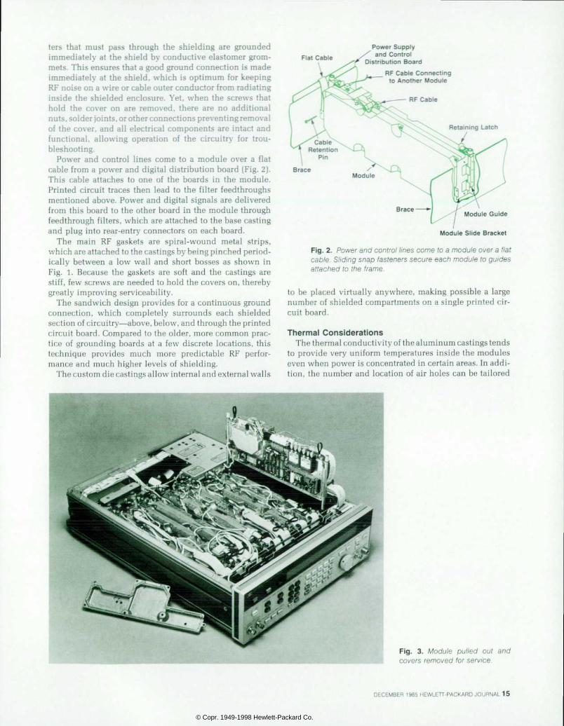
Power and control lines come to a module over a flat cable from a power and digital distribution board (Fig. 2). This cable attaches to one of the boards in the module. Printed circuit traces then lead to the filter feedthroughs mentioned above. Power and digital signals are delivered from this board to the other board in the module through feedthrough filters, which are attached to the base casting and plug into rear-entry connectors on each board.
The main RF gaskets are spiral-wound metal strips, which are attached to the castings by being pinched period ically between a low wall and short bosses as shown in Fig. 1. Because the gaskets are soft and the castings are stiff, few screws are needed to hold the covers on, thereby greatly improving serviceability.
The sandwich design provides for a continuous ground connection, which completely surrounds each shielded section of circuitry — above, below, and through the printed circuit board. Compared to the older, more common prac tice of grounding boards at a few discrete locations, this technique provides much more predictable RF perfor mance and much higher levels of shielding.
The custom die castings allow internal and external walls
Flat Cable Power Supply and Control
Distribution Board
RF Cable Connect ing to Another Module
Brace
Module Guide
Module Sl ide Bracket
Fig. 2. Power and contro l l ines come to a module over a f la t cable. Sl id ing snap fasteners secure each module to guides at tached to the f rame.
to be placed virtually anywhere, making possible a large number of shielded compartments on a single printed cir cuit board.
Thermal Considerat ions The thermal conductivity of the aluminum castings tends
to provide very uniform temperatures inside the modules even when power is concentrated in certain areas. In addi tion, the number and location of air holes can be tailored
F i g . 3 . M o d u l e p u l l e d o u t a n d covers removed for serv ice.
DECEMBER 1985 HEWLETT-PACKARD JOURNAL 15
© Copr. 1949-1998 Hewlett-Packard Co.
to the power being dissipated in each module. Cooling is accomplished by drawing air up through the
modules first, then through the high-performance, dc ball bearing fan, across the power supply rectifiers, and lastly through a heat sink holding the power transistors.
The fan is centrally located in the air flow path and is totally enclosed in the instrument, which greatly reduces the external noise level.
Serviceabil i ty Considerations The modules are mounted in the instrument as shown
in Fig. 2. Two sliding snap fasteners secure each module to guides attached to the internal framework.
A four-color silkscreened diagram on the inside of the instrument top cover provides a detailed map for servicing. An RF connector wrench and fuse puller are mounted in side the instrument.
To replace a module, the two snap fasteners are discon nected, cables are removed, and the module is lifted out and replaced with a known good module. For operating module repair, extender pins are screwed into the tops of the two guides mentioned above. The snap fasteners are then unlatched, the module is pulled up, and the snap fasteners are reconnected at the top of the extenders. The covers can now be removed and the printed circuit boards examined while fully powered-up (see Fig. 3).
Advantages of the Design Because of the conductive elastomer grommets used to
ground the connectors and feedthroughs and the use of a soft RF gasket, access to HP 8642A/B printed circuit boards is obtained by removing only a small number of screws. This provides high serviceability while maintaining very high shielding levels.
The modularity concept, with its fully specified and tested modules, provides high manufacturability and ser viceability. Manufacturability is high since each module's
performance specifications are verified as a separate unit, so that when the modules are assembled into the instru ment, the entire instrument will have a very high likelihood of meeting overall performance specifications. Serviceabil ity is high since modules can be swapped in an instrument in the field and the instrument will still meet its perfor mance specifications.
Liquid Crystal Display Backlighting Because of the serviceability and ease of use goals for
the HP 8642A/B, it was decided that a large alphanumeric display would be required. At the same time, low power consumption and low EMI were important. A liquid-crystal display (LCD) fit all of the requirements. One drawback with LCDs, however, is that they are not readable in the dark. The design team considered this condition unaccept able (even though it often exists) and designed a method of backlighting the display.
Some of the goals for the design were: • Bright, uniform lighting of a very long LCD • Highly reliable light source • Ability to fit in the minimal space behind the LCD.
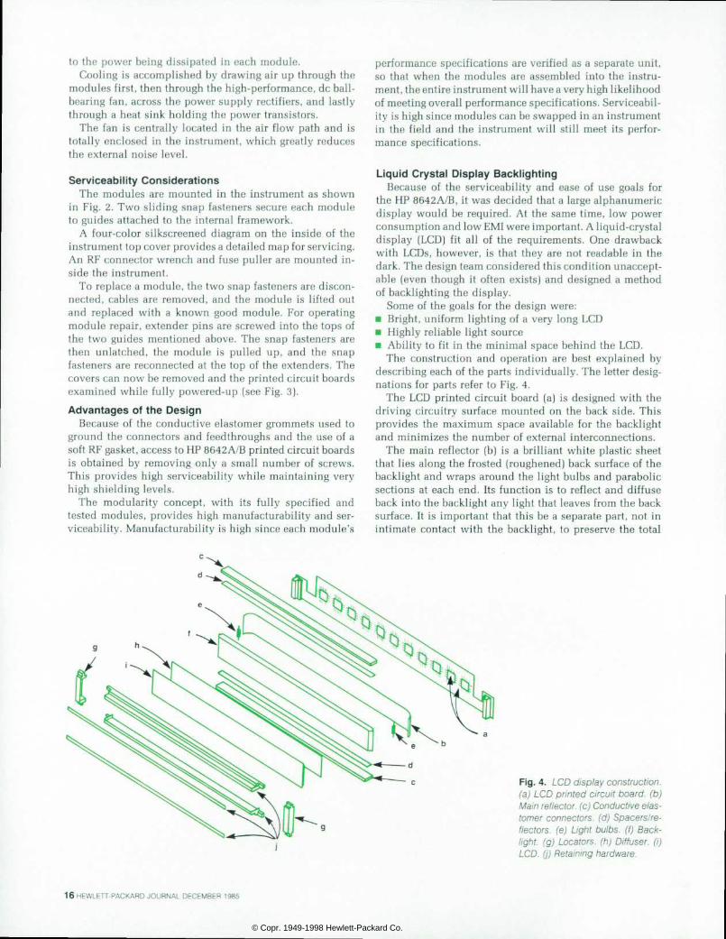
The construction and operation are best explained by describing each of the parts individually. The letter desig nations for parts refer to Fig. 4.
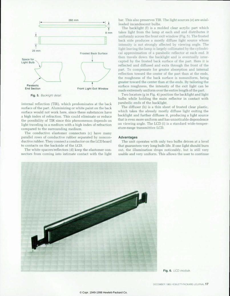
The LCD printed circuit board (a) is designed with the driving circuitry surface mounted on the back side. This provides the maximum space available for the backlight and minimizes the number of external interconnections.
The main reflector (b) is a brilliant white plastic sheet that lies along the frosted (roughened) back surface of the backlight and wraps around the light bulbs and parabolic sections at each end. Its function is to reflect and diffuse back into the backlight any light that leaves from the back surface. It is important that this be a separate part, not in intimate contact with the backlight, to preserve the total
Fig. 4. LCD display construct ion, (a) LCD pr in ted c i rcu i t board, (b) Main reflector, (c) Conductive elas tomer connectors, (d) Spacers/ re f lec tors , (e) L ight bu lbs, ( f ) Back l ight, (g) Locators, (h) Dif fuser. ( i ) LCD. (j) Retaining hardware.
16 HEWLETT-PACKARD JOURNAL DECEMBER 1985
© Copr. 1949-1998 Hewlett-Packard Co.
260 mm
t 8 mm
t 29 mm
Frosted Back Surface
Space for Light Bulb
Parabolic End Section
Fig. 5. Backl ight detai l .
Front Light Exi t Window
internal reflection (TIR), which predominates at the back surface of the part. Aluminizing or white paint on the back surface would not work here, since these substances have a high index of refraction. This could eliminate or reduce the possibility of TIR since this phenomenon depends on light traveling in a medium with a high index of refraction compared to the surrounding medium.
The conductive elastomer connectors (c) have many parallel rows of conductive rubber separated by noncon- ductive rubber. They connect a conductor on the LCD board to contacts on the backside of the LCD.
The white spacers/reflectors (d) keep the elastomer con nectors from coming into intimate contact with the light
bar. This also preserves TIR. The light sources (e) are axial- leaded incandescent bulbs.
The backlight (f) is a molded clear acrylic part which takes light from the lamp at each end and distributes it uniformly across the front exit window (Fig. 5). The frosted back side produces a mostly diffuse light source whose intensity is not strongly affected by viewing angle. The light leaving the lamp is largely collimated by the cylindri cal approximation of a parabolic reflector at each end. It then travels down the backlight and is eventually inter cepted by the frosted back surface of the part. Here it is reflected and diffused and exits through the front of the part. To compensate for greater absorption and internal reflection toward the center of the part than at the ends, the roughness of the back surface is nonuniform, being greater toward the center than at the ends. By tailoring the surface roughness, the intensity of the exit light can be made extremely uniform over the entire length of the part.
Two locators (g in Fig. 4) position the backlight and light bulbs while holding the main reflector in contact with parabolic ends of the backlight.
The diffuser (h) is a thin sheet of frosted clear plastic, which takes the already mostly diffuse light exiting the backlight and further diffuses it, producing a light source that is even more uniform and has unnoticable dependence on viewing angle. The LCD (i) is a standard wide-temper ature-range transmittive LCD.
Advantages The unit operates with only two bulbs driven at a level
that guarantees very long bulb life. If one light should burn out, the illumination drops noticeably, but is still very usable and very uniform. This allows the user to continue
Fig. 6. LCD module.
DECEMBER 1985 HEWLETT-PACKARD JOURNAL 17
© Copr. 1949-1998 Hewlett-Packard Co.
to use the display in a dark environment while scheduling maintenance to replace the bulb. The backlight provides bright, uniform illumination for a very long LCD in the minimum thickness behind the front panel normally needed for standard switches. From service and manufac turing standpoints, the finished, fully tested LCD assembly (Fig. 6) is just another module, which can very easily be swapped, both in the field and on the assembly line.
Acknowledgments Patty Decker-Morton worked on shielding and early at
tenuator concepts. Pat Herrón and Bruce Roeder worked on attenuators. Lee Olmstead contributed greatly to the LCD backlight. Billy Reynolds was invaluable as manufac turing and production engineer. Gene Mertz and others in components engineering were a constant resource.
Many people on the assembly line, in printed circuit board design, quality assurance, the fab and model shop, drafting, lab services, purchasing, and elsewhere in the company contributed ideas, refinements, and energy.
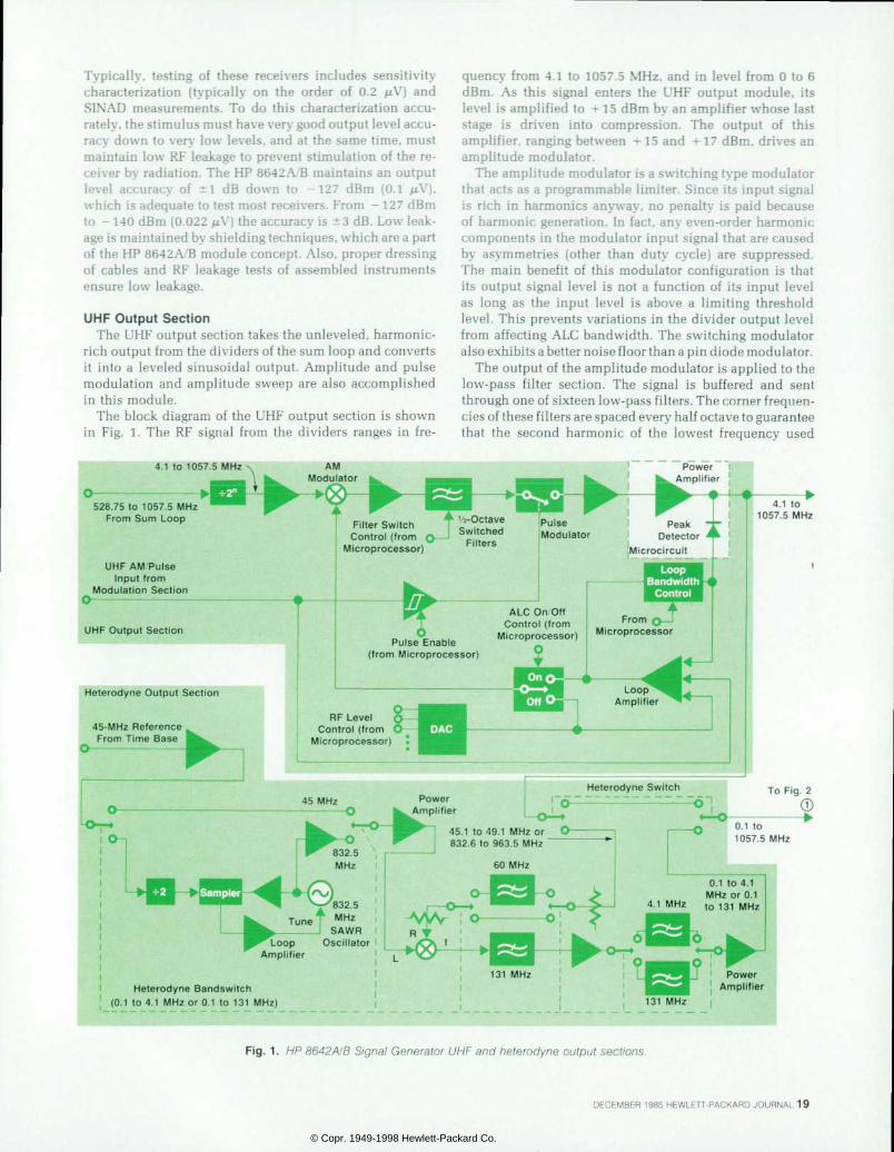
Wide-Frequency-Range Signal Generator Output Section Design by Robert R. Col l ison. James B. Summers, Marvin W. Wagner , and Bryan D. Rat l i f f
TWO OUTPUT SECTIONS are used in the HP 8642A/ B Signal Generator to cover the O.l-to-1057. 5-MHz frequency range. In the HP 8642B, a doubler output
section is added to cover the 1057. 5-MHz-to-21 15-MHz fre quency range.
Fig. 1 is a block diagram of the two output sections — the UHF output section and the heterodyne output section. Fig. 2 is a block diagram of the doubler, attenuator, and reverse power protection section. Both the UHF and the doubler output sections contain power-amplifier/peak-de tector microcircuits and ALC loops. While similar in some respects, these elements are not the same in the two sections and are discussed separately in this article.
The range of 4.1 MHz to 1057.5 MHz is generated by dividing the main octave of 528.75 MHz to 1057.5 MHz with binary dividers (divide by N, where N = l, 2, 4, 8, 16, 32, 64, or 128).
To obtain frequencies from 0.1 MHz to 4.1 MHz, the heterodyne output section is used. The heterodyne LO is a 45-MHz reference signal that originates in the HP 8642A/B time base, and the RF signal is a 45. l-MHz-to-49. 1-MHz signal from the output of the UHF output section (the -^16 band). This selection of heterodyne input frequencies maintains good carrier noise performance and uses a con venient, available LO frequency.
To generate wide-deviation FM with low distortion from 0.1 MHz to 131 MHz (particularly useful for the home entertainment market in the 88-MHz-to-108-MHz range and for characterizing IF amplifiers), the same heterodyne out put section is used, but with higher RF and LO frequencies. Normally, this frequency range is covered by the main oc tave divided by N via the UHF output section. Choosing to divide by N provides the best carrier noise performance, but also divides the amount of FM deviation from the main octave by N. Therefore, N times the amount of FM deviation
is required in the main octave, which increases FM distor tion. By using this heterodyne band, the amount of FM deviation required from the main octave is reduced. This reduces FM distortion for a given FM deviation and in creases FM deviation capability for this frequency range. This benefit is offset by higher carrier noise, which is usu ally not a concern when using large FM deviations. The heterodyne LO for this range is an 832.5-MHz SAWR (sur- face-acoustic-wave-resonator) reference oscillator locked to the 45-MHz reference, and the RF input signal is an 832. 5-MHz-to-963. 5-MHz signal from the UHF output sec tion.
The UHF and doubler output sections have ALC loops to control the output vernier power level and generate the desired AM. In the heterodyne bands, these functions are done by controlling the RF input signal to the heterodyne output section from the UHF output section, since the heterodyne section has no ALC loop. This allows amplitude modulation at low RF frequencies and simplifies ALC bandwidth switching.
Crit ical Design Issues The critical requirements for the output sections were
high output power capability with low RF harmonic distor tion, low output intermodulation distortion, low incidental AM and PM, accurate wide-bandwidth AM with low AM distortion, low residual AM and FM, low noise contribu tion, good RF output impedance, accurate RF output level to very low levels, and reverse power protection. Features added for increased flexibility include amplitude sweep, ALC off, and attenuator range hold. Digitally stored cali bration is used to correct output RF level and AM level to increase accuracy.
One of the prime applications for the HP 8642A/B is as a stimulus for testing very sensitive receivers and pagers.
18 HEWLETT-PACKARD JOURNAL DECEMBER 1985
© Copr. 1949-1998 Hewlett-Packard Co.
Typically, testing of these receivers includes sensitivity characterization (typically on the order of 0.2 pV] and SIN'AD measurements. To do this characterization accu rately, the stimulus must have very good output level accu racy down to very low levels, and at the same time, must maintain low RF leakage to prevent stimulation of the re ceiver by radiation. The HP 8642A/B maintains an output level accuracy of -1 dB down to -127 dBm (0.1 /A'|. which is adequate to test most receivers. From - 127 dBm to -140 dBm (0.022 /xV) the accuracy is ±3 dB. Low leak age is maintained by shielding techniques, which are a part of the HP 8642A/B module concept. Also, proper dressing of cables and RF leakage tests of assembled instruments ensure low leakage.
UHF Output Sect ion The UHF output section takes the unleveled, harmonic-
rich output from the dividers of the sum loop and converts it into a leveled sinusoidal output. Amplitude and pulse modulation and amplitude sweep are also accomplished in this module.
The block diagram of the UHF output section is shown in Fig. 1. The RF signal from the dividers ranges in fre
quency from 4.1 to 1057.5 MHz. and in level from 0 to 6 dBm. As this signal enters the UHF output module, its level is amplified to + 15 dBm by an amplifier whose last stage is driven into compression. The output of this amplifier, ranging between + 15 and + 17 dBm, drives an amplitude modulator.
The amplitude modulator is a switching type modulator that acts as a programmable limiter. Since its input signal is rich in harmonics anyway, no penalty is paid because of harmonic generation. In fact, any even-order harmonic components in the modulator input signal that are caused by asymmetries (other than duty cycle) are suppressed. The main benefit of this modulator configuration is that its output signal level is not a function of its input level as long as the input level is above a limiting threshold level. This prevents variations in the divider output level from affecting ALC bandwidth. The switching modulator also exhibits a better noise floor than a pin diode modulator.
The output of the amplitude modulator is applied to the low-pass filter section. The signal is buffered and sent through one of sixteen low-pass filters. The corner frequen cies of these filters are spaced every half octave to guarantee that the second harmonic of the lowest frequency used
4.1 to 1057.5 MHz
528 .7510 1057 .5 MHz F r o m S u m L o o p
UHF AM Pu l se I n p u t f r o m
M o d u l a t i o n S e c t i o n
U H F O u t p u t S e c t i o n
H e t e r o d y n e O u t p u t S e c t i o n
45-MHz Reference , F r o m T i m e B a s e
F i l t e r Sw i t ch C o n t r o l ( f r o m
M i c r o p r o c e s s o r )
Loop Bandwidth
Control
Pu lse Enab le ( f r o m M i c r o p r o c e s s o r )
ALC On O f f C o n t r o l ( f r o m
M i c r o p r o c e s s o r ) From Q — I
M i c r o p r o c e s s o r
RF Leve l C o n t r o l ( f r o m
M i c r o p r o c e s s o r )
H e t e r o d y n e B a n d s w i t c h (0 .1 to 4 .1 MHz or 0 .1 to 131 MHz)
Power A m p l i f i e r
Fig. sections. . HP 8642 A/B Signal Generator UHF and heterodyne output sections.
DECEMBER 1985 HEWLETT-PACKARD JOURNAL 19
© Copr. 1949-1998 Hewlett-Packard Co.
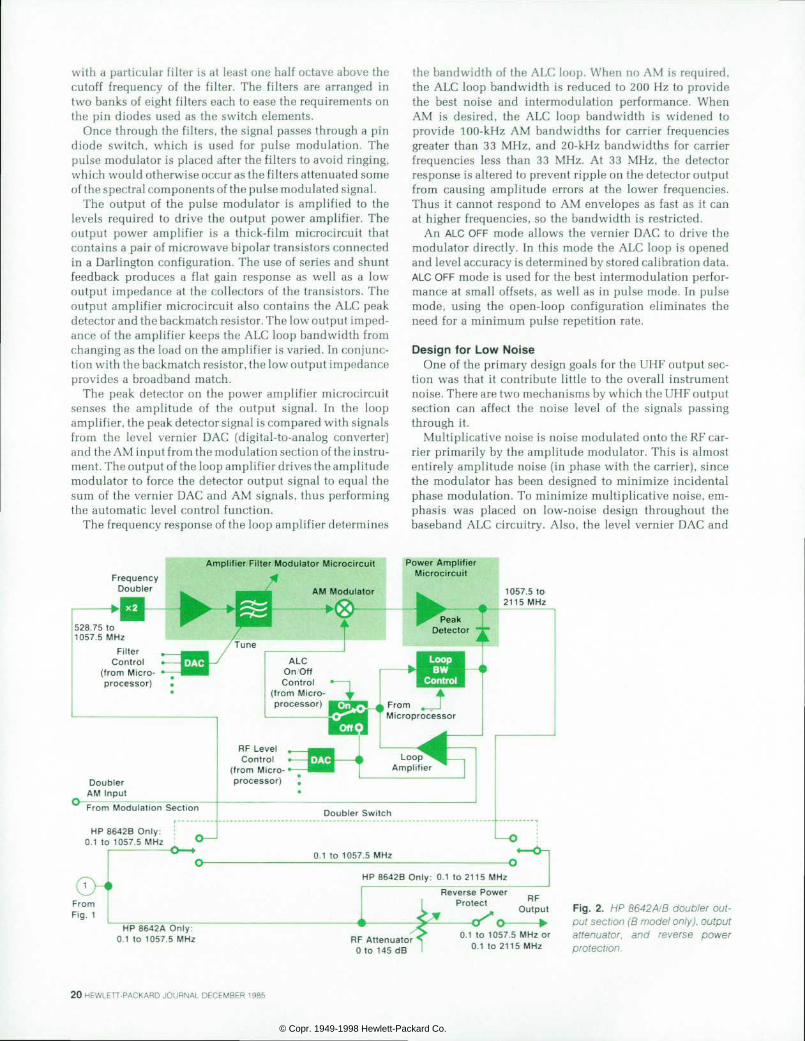
with a particular filter is at least one half octave above the cutoff frequency of the filter. The filters are arranged in two banks of eight filters each to ease the requirements on the pin diodes used as the switch elements.
Once through the filters, the signal passes through a pin diode switch, which is used for pulse modulation. The pulse modulator is placed after the filters to avoid ringing, which would otherwise occur as the filters attenuated some of the spectral components of the pulse modulated signal.
The output of the pulse modulator is amplified to the levels required to drive the output power amplifier. The output power amplifier is a thick-film microcircuit that contains a pair of microwave bipolar transistors connected in a Darlington configuration. The use of series and shunt feedback produces a flat gain response as well as a low output impedance at the collectors of the transistors. The output amplifier microcircuit also contains the ALC peak detector and the backmatch resistor. The low output imped ance of the amplifier keeps the ALC loop bandwidth from changing as the load on the amplifier is varied. In conjunc tion with the backmatch resistor, the low output impedance provides a broadband match.
The peak detector on the power amplifier microcircuit senses the amplitude of the output signal. In the loop amplifier, the peak detector signal is compared with signals from the level vernier DAC (digital-to-analog converter) and the AM input from the modulation section of the instru ment. The output of the loop amplifier drives the amplitude modulator to force the detector output signal to equal the sum of the vernier DAC and AM signals, thus performing the automatic level control function.
The frequency response of the loop amplifier determines
the bandwidth of the ALC loop. When no AM is required, the ALC loop bandwidth is reduced to 200 Hz to provide the best noise and intermodulation performance. When AM is desired, the ALC loop bandwidth is widened to provide 100-kHz AM bandwidths for carrier frequencies greater than 33 MHz, and 20-kHz bandwidths for carrier frequencies less than 33 MHz. At 33 MHz, the detector response is altered to prevent ripple on the detector output from causing amplitude errors at the lower frequencies. Thus it cannot respond to AM envelopes as fast as it can at higher frequencies, so the bandwidth is restricted.
An ALC OFF mode allows the vernier DAC to drive the modulator directly. In this mode the ALC loop is opened and level accuracy is determined by stored calibration data. ALC OFF mode is used for the best intermodulation perfor mance at small offsets, as well as in pulse mode. In pulse mode, using the open-loop configuration eliminates the need for a minimum pulse repetition rate.
Design for Low Noise One of the primary design goals for the UHF output sec
tion was that it contribute little to the overall instrument noise. There are two mechanisms by which the UHF output section can affect the noise level of the signals passing through it.
Multiplicative noise is noise modulated onto the RF car rier primarily by the amplitude modulator. This is almost entirely amplitude noise (in phase with the carrier), since the modulator has been designed to minimize incidental phase modulation. To minimize multiplicative noise, em phasis was placed on low-noise design throughout the baseband ALC circuitry. Also, the level vernier DAC and
Amplif ier Fi l ter Modulator Microcircuit Frequency
Doubler
Power Ampli f ier Microcircuit
528.75 to 1057.5 MHz
Filter Control
( f r o m M i c r o processor)
Doubler AM Input From Modulat ion Sect ion
HP 8642B Only: 0 .1 to 1057.5 MHz
ALC O n O f f Cont ro l • 1
( f r o m M i c r o - X processor)
RF Level Control
( f r o m M i c r o processor)
F r o m , _ I Microprocessor
Doubler Switch
From Fig. 1
0 .1 to 1057.5 MHz
HP 8642B Only : 0 .1 to 2115 MHz
HP 8642A Only: 0 .1 to 1057.5 MHz
3 Reverse Power Protect
V , RF
Output
RF Attenuator ' 0 to 145 dB
0.1 to 1057.5 MHz or 0 .1 to 2115 MHz
F i g . 2 . H P 8 6 4 2 A / B d o u b t e r o u t put sect ion (B model only), output a t t e n u a t o r , a n d r e v e r s e p o w e r protect ion.
20 HEWLETT-PACKARD JOURNAL DECEMBER 1985
© Copr. 1949-1998 Hewlett-Packard Co.
AM signals are summed separately into the ALC integrator. This allows noise from the high-impedance DAC circuitry to be filtered without affecting AM frequency response.
The second noise contribution is additive noise, which results when a signal passes through any stage that contains a noise source. Noise of random phase is added to the RF signal. This noise can be broken into components in phase with the carrier (amplitude noise) and in quadrature with the carrier (phase noise). Additive noise has been minimized by maintaining high RF signal levels throughout the signal path, and by using low-noise stages for amplifi cation and modulation.
The switching modulator offers definite advantages for low-noise operation. First, because its nature is that of a switch, diode current is either zero or twice the signal current for most of the RF cycle. The shot noise contribution of a diode in series with the signal path is inversely propor tional to the square root of the diode current when the diode is biased on. The switching modulator exhibits much higher diode currents when forward-biased than does a pin diode modulator. The second advantage of the switching modulator stems from its limiting nature. Amplitude noise from the divider circuitry is reduced by the limiting action of the modulator, typically by about 10 dB.
Output Power Spike El iminat ion In the design of the UHF output section hardware and
the related processor control firmware, emphasis was placed on the elimination of output power spikes caused by a loss of signal to the ALC loop during divider or oscil lator band changes. When the RF signal drops out, the ALC loop attempts to compensate by increasing the control cur rent to the modulator. When the RF signal reappears, the modulator current may be much too high, causing a momentary high power output from the output power amplifier. To prevent this, during band changes the vernier DAC is set to zero and a built-in offset within the DAC prevents the ALC integrator from slewing the modulator current towards full on.
Another potential cause of signal loss in the ALC loop occurs when low-pass filter switchpoints are crossed. To prevent this, the processor always switches the low-pass filters such that the initial and final frequencies are in the filter passband during the frequency transition. Moving up in frequency, the new higher-cutoff-frequency filter is switched in before anything else happens. Moving down in frequency, the current filter is left in until the frequency transition has occurred, and then the correct filter is switched in.
Calibrat ion and Diagnostics To take full advantage of the powerful microprocessor
that controls the instrument, an analog multiplexer is de signed into the UHF section circuitry to monitor key voltage levels. Most mechanical adjustments have been eliminated and replaced by microprocessor-controlled DAC adjust ments. All test points necessary for calibration and opera tional verification are brought out through the multiplexer.
Output level calibration is a two-stage process. First the gain and offset of the vernier DAC are characterized, and then the frequency response of the RF peak detector in the
power amplifier is determined. Corrected level accuracy at the output of the UHF output section is typically ±0.1 dB over the 4.1-to-1057.5-MHz frequency range.
Amplitude modulation depth is calibrated by charac terizing the detector diode at 17 frequencies. The detector diode is an offset from its ideal characteristic that is dependent upon stray reactances. This offset is measured and stored as correction data. When setting AM depth, the processor uses this offset data and the level vernier DAC voltage to compute the AM voltage required from the mod ulation section.
As mentioned earlier, operation in ALC OFF or pulse modes depends on calibration data for level control. Here, the output power as function of the level vernier DAC setting is characterized at 22 frequency points and two levels at each frequency. A double interpolation is used to set any arbitrary level at any arbitrary frequency.
Ampli tude Sweep A useful feature of the HP 8642A/B is amplitude sweep.
The output amplitude can be swept over a O-to-20-dB range either linearly or logarithmically. This allows such mea surements as amplifier compression testing, log amplifier testing, and detector linearity testing. Amplitude sweep is done with the ALC loop closed to provide good amplitude accuracy and linearity.
Heterodyne Output Section The heterodyne output section is designed to frequency
translate the RF output signal from the UHF output section by means of a mixer and very linear RF and IF paths. In the process, both AM and FM pass through virtually un changed. The heterodyne output section uses bipolar tran sistor amplifiers, LC filters, a doubly balanced mixer, a SAWR oscillator, a FET switch, and pin diode switches. The SAWR oscillator and sampling phase-locked loop used for the LO in the O.l-to-131-MHz band are very similar to those in the frequency synthesis section (see article, page 24) and are not discussed here. The heterodyne switch uses a ceramic substrate with TO-5 relays similar to the output attenuator (see below); it is used to switch the heterodyne section in or out as desired.
As previously mentioned, two heterodyne bands are im plemented in the HP 8642A/B to allow the user to choose between a lower-noise output signal or wider-deviation FM capability. This creates special design challenges, since several circuits have to perform well for two ranges of heterodyne section RF input frequencies that are approxi mately 800 MHz apart in frequency. In some cases, this requires that two different circuits be used. Switching be tween these circuits is accomplished using pin diode switches and TTL drive circuitry. In both bands, the overall gain of the heterodyne output section is nominally unity.
There were two major design challenges for this section. The first is the suppression of unwanted (spurious) signals generated during the frequency translation process. The guaranteed specification for these nonharmonically related signals is that they are more than 100 dB below the carrier in the O.l-to-4. 1-MHz band. The second challenge is the preservation of the desirable characteristics of the UHF 'Th is accuracy excludes errors in the measur ing inst rument
DECEMBER 1985 HEWLETT PACKARD JOURNAL 21
© Copr. 1949-1998 Hewlett-Packard Co.
output section signal, such as level accuracy, spectral pur ity, and modulation.
Spurious-Signal Considerat ions The two primary mechanisms for the generation of spuri
ous signals in the heterodyne section are mixing products and leakage. Since all the amplifiers in the RF signal path are designed to be extremely linear, the only significant source of undesired mixing products is the mixer. To minimize the level of these spurious signals, a high-level mixer is used and the RF level presented to the mixer is kept relatively low. There is approximately 26 dB of attenu ation between the heterodyne section input and the RF port of the mixer. Further attenuation of this signal would seriously degrade its signal-to-noise ratio, so it is important that the mixer have low spurious response.
It is also necessary to include switched low-pass filters in both the RF and IF paths (see Fig. 1). The switched 60-MHz low-pass filter is used in the 0.1-to-4.1-MHz band to reduce the harmonics of the RF signal input to the mixer so that they will not mix with harmonics of the LO signal and create spurious signals that cannot be filtered out later. The switched 4.1-MHz or 131-MHz filters in the IF path are used to filter out mixing products that are higher in frequency than the highest-frequency signal desired from the selected heterodyne band. For the higher-frequency heterodyne band, two five-pole filters are used to achieve the desired rejection. In the lower-frequency heterodyne band, one seven-pole filter is sufficient.
Crit ical Components Selection of the pin diodes used to switch the low-pass
filters is based upon three important parameters that are all critical to the performance of the circuit. The first impor tant parameter is off capacitance. If the capacitance is too high, spurious signals are able to couple around the filters that are designed to reject them. This is especially true in the IF path, where two filters run parallel and one has a much higher bandwidth than the other. The second impor tant parameter is insertion loss. Since the entire heterodyne section runs open-loop, it is important that the diodes have a very consistent forward resistance from diode to diode. This allows repeatable gain characteristics from module to module. The last important parameter of the pin diodes is low-frequency response. The insertion loss of the diodes has to be flat down to 100 kHz so as not to distort the amplitude modulation and frequency characteristics of sig nals with sideband frequencies as low as 100 kHz. Selecting diodes that can meet all three of these requirements simul taneously was a real challenge: however, a diode and a design meeting all the requirements were found.
Thermal Considerat ions As previously mentioned, the heterodyne section is de
signed for a nominal gain of unity. Spurious-signal consid erations require that the RF input signal to the mixer be severely attenuated. This results in a down-converted sig nal attenuated by more than 30 dB that must be amplified back to its original level. To meet HP class B environmental specifications, the circuit has to work from 0°C to 50°C with less than 0.2 dB variation in net gain, including mixer
conversion loss, pin diode insertion loss, attenuator losses, and amplifier gains, all of which vary with temperature. Compensation for all these factors is achieved with a single two-element series network.
A thermistor in series with a resistor is added to the emitter circuit of one of the three amplifier stages. This thermistor has a negative temperature coefficient; as the temperature increases, its resistance decreases and the net gain of the amplifier increases. This compensates for all of the other temperature effects, which have a net effect of lowering the gain with increasing temperature. By adjust ing the nominal resistance of the thermistor and resistor as well as the temperature sensitivity of the thermistor, a net gain variation of less than 0.2 dB over the specified temperature range is achieved.
Doubter Output Section The primary function of the doubler section is to extend
the upper frequency limit of the HP 8642B from 1057.5 MHz to 2115 MHz. Fig. 2 shows the overall doubler block diagram.
The input signal that drives the doubler module comes from the UHF output section. The input signal's level is + 16.5 dBm and its frequency is between 528.75 and 1057.5 MHz. The frequency doubler is a full-wave bridge rectifier with four diodes that are contained within a single package. This reduces parasitics and improves diode-to-diode matching, which enhances doubler performance. The bridge is driven by a balun made from coaxial cable and ferrite beads to simulate inductors at the frequency of op eration. The output signal from the doubler is at twice the input frequency. In addition to the doubled frequency, there are also nf0/2 subharmonics, where n = 1,3,4,5... and f0 is the desired output frequency. These subharmonics are as high as —15 dBc and must be filtered with a tunable bandpass filter that operates from 1057.5 to 2115 MHz. To overcome the 1 2 dB of conversion loss in the doubler circuit and to minimize additive noise, a gain stage follows the doubler circuit to maintain a good signal-to-noise ratio.
Amplif ier/Filter/Modulator Microcircuit The signal level in the amplifier/filter/modulator micro-
circuit is increased by 9 dB by a single-stage GaAs FET amplifier that has a flat gain response.
Since the doubled signal has nf0/2 subharmonics as high as - 15 dBc, a tunable bandpass and notch filter that oper ates over the entire doubler frequency range is used to reject the subharmonics by 35 to 40 dB. Two input lines to the filter control the passband and notch response. The calibration of the filter is critical if the subharmonic perfor mance specification is to be met. The microprocessor con trols an eight-bit DAC such that when all the digital inputs are at a logic low level, the filter is centered about 1057.5 MHz. When all digital inputs to the DAC are at a logic high level, the filter is centered about 2115 MHz. When charac terizing the filter's response, the DAC is set to 33 known states and the 3-dB bandwidth is determined. The center frequency can be calculated from the 3-dB frequencies of each state so that for a given frequency setting an exact DAC number can be calculated to tune the filter properly. From the 33 known DAC numbers and center frequencies,
22 HEWLETT-PACKARD JOURNAL DECEMBER 1985
© Copr. 1949-1998 Hewlett-Packard Co.
the remaining states are interpolated. When the frequency setting changes by more than 5 MHz, the microprocessor updates the DAC number to tune the filter to the proper center frequency.
The RF signal amplitude is controlled through the use of a two-section pi-configuration modulator to achieve 0.1- dB output level resolution and to provide amplitude mod ulation. The control devices are pin diodes whose RF resis tance, which depends on the amount of dc bias current, determines the RF attenuation. The dynamic range of the modulator is 40 dB. Harmonics on the output of the ampli tude modulator are less than — 40 dBc, while subharmonics are less than - 55 dBc. With the modulator set for minimum insertion loss, its nominal RF output level is + 2 dBm.
P o w e r A m p l i f e r a n d P e a k D e t e c t o r M i c r o c i r c u i t The power amplifier, which follows the amplifier/filter/
modulator microcircuit, provides the necessary output power to meet the RF power specification for the instrument.
The input signal received from the amplifier/filter/mod- ulator microcircuit must be increased in signal level to provide the necessary output power. This is accomplished through the use of a two-stage GaAs FET amplifier which uses feedback to maintain a flat gain response. The first stage has a drain voltage of +5V and a drain current of 220 mA. The second state has a + 7V regulator and a drain current of 230 mA. The overall gain provided by the output amplifier is +18 dB.
The RF peak detector, which is also located in this assem bly, is used to sense the RF level on the drain of the output stage. The detector uses two diodes in series, which reduces the junction capacitance to provide the desired frequency response and increases the breakdown voltage capabilities to meet the RF power requirements. A temperature com pensation circuit, containing two diodes similar to the de tector diodes, cancels the effects of the detector diodes' junction voltage temperature dependence.
The peak detector conducts on the negative RF peaks, generating a dc voltage proportional to the RF power level. This detected dc signal is fed to the input of the loop amplifier, which drives the modulator, which adjusts the RF level to provide the desired output power. This feedback loop is the doubler ALC loop (not the same as the UHF output section ALC loop).
Doubler ALC Loop The integator has selectable time constants for changing
the ALC loop response. If AM or amplitude sweep is selected, the loop bandwidth is 100 kHz. For continuous wave (CW) operation, the ALC loop can be narrowed to reduce noise components. This also improves the third- order intermodulation distortion products because the loop has less bandwidth to respond to an external signal applied to the output.
There are three other modes of operation in the doubler ALC loop. The first is amplitude sweep. Under normal ALC loop operation the vernier's range is from + 5 to +16 dBm. In the case of amplitude sweep, the vernier is extended down to a minimum of — 15 dBm. This is achieved by the processor's sending digital data to the vernier DAC. The result is that the vernier is swept in a linear or log mode
to yield an accurate amplitude sweep over a 20-dB range for a given frequency setting. This function is useful for compression tests on amplifiers' and for detector linearity checks.
The next mode of operation is the ALC off mode. Under this condition the ALC loop is opened by a pair of FET switches. One of these FET switches, attached to the output of the ALC loop amplifier, is opened. The second FET switch, which is closed, is connected to the output of the vernier DAC. This allows the vernier DAC to drive the modulator voltage control line directly and set the mod ulator to a desired attenuation level. This provides the best third-order intermodulation distortion products since the detector can no longer respond to an external signal that falls within the ALC loop bandwidth. These intermodula tion products are improved to the level of the nonlinearities found in the power amplifier.
Pulse Operation The next mode of operation is pulse modulation. Pulse
mode in the doubled band also operates with the ALC circuitry turned off. The pulsed RF signal is generated in the UHF output section rather than in the doubled band to provide a much better on/off ratio. The doubler is set to a fixed RF level in the ALC off mode to give the desired output power. As the UHF RF signal level drops, the dou bler circuit conversion loss increases drastically since the diodes no longer conduct, thereby improving the on/off ratio by 40 dB. This yields a doubler band on/off pulse specification of 80 dB.
Attenuator Considerat ions The HP 8642A and HP 8242B use different types of RF
output attenuators. The HP 8642 A uses two step attenuators in series, which provide 0 to 145 dB of attenuation in 5-dB steps. One attenuator has up to 85 dB of attenuation and the other has up to 60 dB of attenuation. The reverse power protection circuit is a part of the 60-dB attenuator. Both attenuators use thick-film resistor network attenuator sec tions on ceramic substrates with TO-5 style miniature re lays to switch the various sections in or out. The substrates are mounted inside individual metal housings.
Separation of the attenuators into two separate housings aids in maintaining input-to-output isolation when large amounts of attenuation are desired. For example, when 135 dB of attenuation is desired, stray leakage from at tenuator input to output must be lower than 153 dB to maintain an attenuation error of less than 1 dB. Even though the HP 8642A/B has digitally stored corrections for at tenuator accuracy, the amount of leakage must be low for the attenuator to be correctable within the vernier con straints of the output section. The low leakage is. also re quired to meet instrument RF leakage specifications.
The HP 8642B also uses two attenuators. However, since the frequency range is higher (2115 MHz), two microwave stripline style attenuators are used to maintain better im pedance characteristics, more accurate attenuation, and lower insertion loss. These two attenuators provide 0 to 145 dB in 5-dB steps. One attenuator has up to 70 dB of attenuation and the other has up to 75 dB of attenuation. Both use thin-film resistor networks as attenuator sections
DECEMBER 1985 HEWLETT-PACKARD JOURNAL 23
© Copr. 1949-1998 Hewlett-Packard Co.
and have solenoid-actuated stripline switches to switch the various sections in or out. As in the HP 8642A, the two separate attenuators aid in maintaining isolation. This is even more difficult in the HP 8642B because of the higher frequency range. The reverse power protection circuit in the HP 8642B is on a separate board in another housing.
As mentioned before, the HP 8642 A/B has digitally stored correction for attenuator accuracy. There are correction data points approximately every 60 MHz for every 5-dB step in attenuation. This totals about 600 correction points for an HP 8642 A and 1140 correction points for an HP 8642B. This sizable amount of data is generated at a level accuracy test station where it is stored in the HP 8642A/B memory. The HP 8642A/B interpolates correction values between frequency data points to get the best level accu racy. At the same level accuracy test station, each HP 8642A/B is verified for level accuracy by measuring levels midway between correction frequencies. This method is sensitive to any leakage problems that might otherwise not be detected by simply checking at the correction frequen-
Reverse Power Protect ion The function of the reverse power protection circuit is
to prevent damage to the attenuator and output amplifier caused by the application of excessive RF power to the RF output connector. The circuit detects the signal level at the RF output connector and opens a relay in the signal path when a reverse power situation occurs. During the time required for the relay to respond (approximately 50 /xs), a diode limiter circuit prevents more than 1 watt from reach ing the attenuator or power amplifier. The design goals for the reverse power protector included, in addition to the
protection function, low loss and low VSWR. To accomplish the design objectives to a frequency of
2100 MHz, a special reed relay was developed. In this relay, the reed capsule forms the center conductor and dielectric of a coaxial transmission line. The outer conductor is formed by a rolled brass shield and a conductive coating on the capsule itself. The relay is soldered into a microstrip circuit, which also contains a limiter and a dc blocking capacitor. The limiter consists of a pair of pin diodes and two Zener diodes which set the limiting level. Limiting begins when the RF level reaches 10 volts peak. A detector senses the level at the limiter and signals the relay to open when the RF level reaches approximately 7 volts peak.
The reverse power protection circuit typically has inser tion loss less than 1 dB and VSWR less than 1.25 to 2100 MHz. The maximum power capability is 50 watts in an HP 8642A and 25 watts in an HP 8642B.
Acknowledgments We would like to thank Art Upham for his tireless leader
ship and long hours as the HP 8642A/B program manager. Also, we would like to thank Dick Waite, Eric Pirttima, and Alden Forbes of our microcircuit development area and the people of the HP Microwave Technology Division for their assistance in developing HP 8642A/B microcir- cuits and SAW devices. In addition, we wish to thank our printed circuit designers, assembly and test engineers, and Don Borowski and Tom Yeager for their assistance in de velopment of the output sections. A very special thanks goes to Eric Anderson of our product assurance area for his tireless assistance in rigorous environmental testing of the HP 8642A/B during its development.
Signal Generator Frequency Synthesizer Design b y T h o m a s N i e m a n n F a u l k n e r , E a r l C . H e r l e i k s o n , R o n a l d J . M a y e r , B r i a n M . M i l l e r , a n d M a r k A . N i e m a n n
THE FREQUENCY SYNTHESIZER of the HP 8642 A/B Signal Generator is designed to minimize the phase noise, spurious response, and switching speed of the
instrument, while optimizing its angle modulation capabil ities. This design challenge was met by dividing the fre quency synthesis process into component phase-locked loops, which were then individually optimized for their specific function.
The six component phase-locked loops are the time base, the FM loop, the SAWR (surface-acoustic-wave-resonator1) loop, the reference loop, the IF loop, and the sum loop. Fig. 1 , a general block diagram of the frequency synthesizer, shows the loops' interrelationships.
The time base produces the 10-MHz time base output, a 500-kHz reference for the FM and IF loops, and a 45-MHz reference for the counter, SAWR loop, and the heterodyne reference loop of the output section (see article, page 18). It uses its internal 45-MHz reference oscillator, or it will automatically lock to an externally supplied 1-MHz, 2- MHz, 5-MHz, or 10-MHz reference source.
The FM loop is a 135-MHz reference that provides low- distortion, high-accuracy angle modulation.
The SAWR loop provides the reference loop with three spectrally pure UHF reference frequencies. Using these three references, the reference loop translates the FM loop's angle modulation into six UHF frequencies.
24 HEWLETT-PACKARD JOURNAL DECEMBER 1985
© Copr. 1949-1998 Hewlett-Packard Co.
44.8 to 90.2 MHz 1-Hz to 0.05-Hz Steps
528.75 to 1057.5 MHz 1-Hz to 0.05-Hz Steps Af = 0 to 1 .5 MHz F M = D C t o 2 0 0 k H z To ^2" C i rcu i t
Modulation DC to 200 kHz
135 MHz Af = O to 1 .5 MHz
, F M = D C t o 2 0 0 k H z
6 0 7 . 5 M H z 8 7 2 . 5 M H z 6 5 2 . 5 M H z 9 2 2 . 5 M H z 6 9 7 . 5 M H z 9 6 7 . 5 M H z Af = 0 to 1 .5 MHz F M = D C t o 2 0 0 k H z
Reference Loop
10-MHz Output
Fig . 1 . S ix phase- locked loops make up the f requency syn thesizer sect ion of the HP 8642A/B Signal Generator .
The IF loop is a fractional-N synthesizer that produces a spectrally pure VHP reference from 44.8 to 90.2 MHz in steps as small as 0.05 Hz.
Using the IF reference frequencies, the sum loop trans lates the six reference loop frequencies to produce the fun damental octave of the instrument. Thus the sum loop out put has the full angle modulation capability of the FM loop, the frequency resolution of the IF loop, and nonhar- monically related spurious levels of less than - 100 dBc for carrier offsets greater than 10 kHz maintained by all loops.
Loop Structures The time base (Fig. 2) and SAWR (Fig. 3) loops are sam
pling phase-locked loops. They use sampling phase detec tors to multiply the reference frequency up to the loop's output frequency. The output of a sampling phase detector •The and reso lu t i on o l t he IF l oop i s 1 Hz i n the undoub ied band and 0 .5 Hz i n the doubled band (above 1057 5 MHz in the HP 8642B). A special function provides resolut ions of 0.1 Hz and 0 05 Hz. respect ive ly
is a voltage proportional to the phase difference of the sampled output frequency and the reference frequency. The detector's output is integrated, then used to control the relative phase of the loop's voltage-controlled crystal oscillator (VCXO), producing a phase-locked output.
The FM (Fig. 4) and IF (Fig. 5) loops are divider phase- locked loops. They use digital frequency dividers to divide the voltage-controlled oscillator's (VCO's) output frequency down to the reference frequency, which is fed into the digital phase/frequency detector. The detector's output is integrated and sent to the VCO's control voltage input. If the reference and divided VCO signals are at different fre quencies, a dc offset voltage will be produced that forces the integrator to move the VCO toward the reference fre quency. Once the reference and divided VCO signals have reached the same frequency, the detector's output is pro portional to the phase difference of the two signals and forces the loop output to be phase-locked to the reference. The IF reference loop has the additional design constraint of a 0.05-Hz frequency resolution, which was met by using a fractional-N phase-locked loop.
The fractional-N technique allows the use of effective noninteger divide numbers. It involves switching between two integer divide numbers with varying duty cycles. Sev eral additions are made to a conventional phase-locked loop to make it a fractional-N loop.
When the divide number is not an integer, the divider output does not equal the reference frequency. This causes an increasing phase offset, which sends more current into the loop integrator. This is compensated for by adjusting the amount of phase correction current. The output of the integrator is shown in Fig. 6. The phase detector causes a ramp up in voltage. The phase correction current causes a ramp down. The phase correction is adjusted to make these two ramps equal in length.
The phase difference between the two phase detector inputs is accumulated digitally in the fractional-N 1C and applied to the phase correction current sources. This phase correction is limited to 360° by practical limitations of the phase detector hardware. When one complete cycle of extra phase is accumulated, the fractional-N 1C instructs the di vider to "swallow" one pulse of the VCO output. This gives the signal applied to the phase detector an average fre-
External Reference
Sensor
Internal T ime Base
DC Reference
External T ime Base
Input
500-kHz Reference
10-MHz Output
F ig . 2 . T ime base loop b lock d ia gram.
DECEMBER 1985 HEWLETT-PACKARD JOURNAL 25
© Copr. 1949-1998 Hewlett-Packard Co.
Integrator
45 MHz
Fig . 3 . SAWR (sur face-acous t i c - w a v e - r e s o n a t o r ) l o o p b l o c k d i a gram.
quency of 100 kHz. The accuracy with which the up and down ramps can
be equalized determines the level of sidebands on the loop output. If these ramps are different the output appears to jump between two frequencies. The HP 8642A/B hardware is capable of correction that results in spurious levels of - 60 to - 65 dBc. This is further reduced by loop filtering, as explained later.
The sum (Fig. 7) and reference (Fig. 8) loops are summing phase-locked loops. They produce the sum or difference of two reference frequencies with minimal spurious signals by mixing the loop's UHF output with a UHF reference to produce an intermediate frequency signal. This signal is then filtered and amplified and sent to a phase detector. The phase detector's output is a voltage proportional to the phase difference of the detector's VHF reference and the intermediate frequency signal. The detector's output is then integrated and used to control the loop's VCO. To ensure that the loop locks to the correct mixer sideband, the VCO is pretuned to within 7.5 MHz of the loop's output frequency. The trade-off between phase noise and spurious outputs is optimized by adjusting the VCO's tuning sen sitivity to produce a constant loop bandwidth of 1.8 MHz.
Minimizing Phase Noise Within its bandwidth, a phase-locked loop will track the
effective noise of its reference signals. This effect can make a low-noise voltage-controlled oscillator more noisy, or a
noisy VCO more quiet, depending on the loop bandwidth, the open-loop VCO noise performance, and the effective noise of the reference signal. The effective reference noise for a frequency-multiplying loop is the reference noise in creased by the multiplication factor. The effective reference noise of a summing loop is the sum of the references' noise. Outside of its bandwidth, the noise of a phase-locked loop is the sum of the open-loop VCO noise, the buffer amplifier noise floor, and the effective reference noise lowered by — 20 log (carrier offset frequency + loop bandwidth) dB.
The time base and the FM, SAWR, and IF loops are all multiplier-type loops, and have in common narrow loop bandwidths and VCOs with narrow tuning ranges and low phase noise. Narrow loop bandwidths prevent multiplied reference noise from degrading the VCO noise. The sum and reference loops are summing-type loops and have in common wide loop bandwidths and moderate-noise, wide- tuning-range VCOs.
All the oscillators in the instrument are designed for low noise.2 For its particular application, each oscillator is op timized with the lowest practical white noise floor and with a resonator of the highest practical Q and lowest prac tical 1/f noise corner. Degradation of resonator Q from res onator switching circuitry has been eliminated by switch ing entire oscillators instead of individual resonators.
The SAWR loop employs three surface-acoustic-wave- resonator (SAWR) oscillators. The SAW resonators were specially developed by HP Laboratories to meet the low
FM
Audio Modulating
Signal
P M
PM Crossover
F M F M Crossover
500 kHz from
T ime Base
125-kHz Reference
PM
Phase/Frequency Detector
VCO Frequency ^ 1 0 8 0 t o C o u n t e r '
DCFM Vol tage
Reference
I h O D C F M T 135-MHz Output
ACFM ' T u n e M'V
Loop Filter 135-MHz
VCO
Fig . 4 . FM loop b lock d iagram.
26 HEWLETT-PACKARD JOURNAL DECEMBER 1985
© Copr. 1949-1998 Hewlett-Packard Co.
Pulse Remover
(Swallower)
100 kHz
I Phase Detector | Current Source
Integrator Samp le Ho ld
Bu f fe r Shaper-Filter
Sample Hold Control
Phase Correction Current Sources
phase noise and frequency pull requirements of the HP 8642 A/B at UHF frequencies. The SAW resonators are mul tiple-cavity resonators and provide a low source resistance (Rs) with transverse modes far from the center frequency. The low Rs provides a wide frequency pulling range (>300 ppm) with inexpensive varactors. Low Rs also minimizes loop-gain loss without the need for matching transformers, thus reducing frequency drift caused by external compo nent tolerances.
The FM, IF, sum, and reference loops all use varactors especially selected for high Q and low 1/f noise corner. A well-filtered 50V power supply operates the varactors in the upper two thirds of their voltage range to maximize their Q. VCO sensitivity to control-line noise is minimized by limiting VCO tuning sensitivity.
To meet the instrument noise performance goals, six VCOs are used in the IF loop, two in the reference loop, and four in the sum loop. The IF and FM loop VCOs use inductor/varactor resonators, with inductor geometry op timized for maximum Q in the space available. The varac tors are preselected for low noise by testing them in a VCO inside a phase-locked loop. The gain stages for these oscil lators consist of a source-follower and a common-gate amplifier. The common-gate stage provides the necessary gain to support oscillation. The source-follower provides an impedance buffer to reduce loading of the resonant cir cuit by the common-gate stage. This increases the loaded Q of the resonator, which improves the phase noise perfor mance. The feedback is obtained with capacitors used as impedance transformers. This minimizes loading, sets the proper loop gain, and provides the necessary phase shift for oscillation.
The sum and reference loop VCOs use transmission-line/ varactor resonators, built on Teflon'Vglass printed circuit boards. Their circuit configuration is that of a Hartley oscil lator modified to operate with high Q at high frequencies (Fig. 9). At frequencies above fhfe (3-dB corner of hfe), a tran sistor's ft (h(e in the common-emitter configuration) has an additional 90° of phase lag because of base diffusion capacitance. This phase lag of the transistor at high frequen cies is compensated by the phase lead of the series capaci tance of the base and collector. The amplifier circuit now has the necessary 180° phase shift which, when added to
à 44.8 to 90.2 MHz 1-Hz. 0.5-Hz, 0.1-Hz,
P r e t u n e o r 0 . 0 5 - H z S t e p s
F i g . 5 . I F l o o p b l o c k d i a g r a m . This loop is a fract ional-N loop.
the 180° phase shift of the resonant circuit, produces the 0° phase shift necessary for oscillation.
High Q is achieved by tapping down on the transmission line inductors with both the base and collector, which have approximately 15Ã1 and 50Ã1 load and source impedances, respectively. This leaves the Q to be set primarily by the tunable element of the tank circuit, the varactor. The un loaded Q is greater than 100, and the loaded Q is greater than 60.
Minimizing Spurious Responses Several design procedures ensure that the HP 8642A/B
meets its design goal that all nonharmonically related spurious outputs be less than - 100 dBc at offsets greater than 10 kHz from the carrier. To prevent spurious leakage and electromagnetic interference (EMI), beryllium-copper spiroshield gaskets and conductive elastomer are used in the die-cast aluminum housings. Noncritical cables are triple-shielded coax, critical RF cables are semirigid coax, and all power supply and digital control lines through module walls are bypassed with feedthrough filters.
Steel support frames and MuMetalâ„¢ in critical areas pre vent modulation of sensitive narrow-bandwidth phase- locked loops via magnetic coupling from the power trans former. The time base, FM, IF, and SAWR loops, and the high-stability 10-MHz reference (Option 001) are shock-
Sample
Phase , Correction
Cur ren t On
-One Reference Cyc le (10 us)
Fig. 6. IF loop in tegrator output waveform.
DECEMBER 1985 HEWLETT-PACKARD JOURNAL 27
© Copr. 1949-1998 Hewlett-Packard Co.
IF Loop Input 44.8 to 90.2 MHz
R e f e r e n c e 6 0 7 . 5 8 7 7 . 5 L o o p 6 5 2 . 5 9 2 2 . 5 I n p u t 6 9 7 . 5 9 6 7 . 5
M H z M H z Fig . 7 . Sum loop b lock d iagram.
mounted in the instrument to prevent mechanical vibration from modulating sensitive VCOs. The IF and FM oscillator inductors are dampened with vibration-absorbing foam to reduce microphonically induced FM.
Amplifiers in the feedback path of each loop are used to prevent spurious signals from appearing on the loop out puts. Sampling spurious from the phase detectors of the time base and SAWR loops, divider spurious from the FM and IF loops, and UHF reference and phase detector spuri ous in the sum and reference loops are thus eliminated. Output path buffer amplifiers are used to prevent signals from moving backwards through the synthesizer and pro ducing spurious signals in otherwise spectrally pure refer ences. The buffer/limiters used for spurious isolation are designed to prevent baseband noise from upconverting around the carrier. This is accomplished by diplexing each amplifier stage output such that low-frequency noise is terminated in a 50Ãà load and the desired signal is passed on to the next stage. VCO spurious resulting from phase detector feedthrough and harmonics is attenuated by loop filters and integrators. Phase-locked loops also act as low- pass filters. Spurious signals generated inside the loop bandwidth remain constant, while those generated outside the bandwidth are attenuated by - 20 log (spurious offset frequency •* loop bandwidth) dB. In the IF loop, the frac- tional-N divider produces spurious of —60 to —65 dBc. A 200-Hz loop bandwidth and a one-pole low-pass filter at
1 kHz provide an additional 54 dB of spurious attenuation at 10 kHz, producing a total spurious performance of less than - 110 dBc at offsets greater than 10 kHz.
The sum and reference loops' mixer spurious outputs are unfilterable within the loops' 1. 8-MHz bandwidths. The mixers were especially built and selected for low spurious. Impedance matches at all ports, power levels at the LO and RF ports, and minimal harmonics at the RF port are all carefully maintained to avoid degrading mixer spurious performance. Mixer output power is optimized to provide minimum spurious with minimal phase noise degradation.
Minimizing Frequency Switching Time and Phase Acquisi t ion Time
The instrument's frequency switching time is set by the IF loop to typically 70 ms, during which time the SAWR, reference, and sum loops are also switched. The FM and time base loops do not change frequency during standard instrument operation. Switching and acquisition times are inversely proportional to the loop's bandwidth. This limi tation is overcome in the IF and SAWR loops by widening the loop bandwidths during phase acquisition. The IF loop increases switching speed by pretuning the VCOs, and widens loop bandwidth using a speedup circuit that re duces the attenuation in the loop's lead/lag filter whenever there is a rapid change in the integrator output voltage. The SAWR loop senses an out-of-lock condition and increases
FM Loop Input
135 MHz
SAWR Loop Input 742.5 MHz 787.5 MHz 832.5 MHz
Fig . 8 . Re fe rence loop b lock d ia gram.
28 HEWLETT-PACKARD JOURNAL DECEMBER 1985
© Copr. 1949-1998 Hewlett-Packard Co.
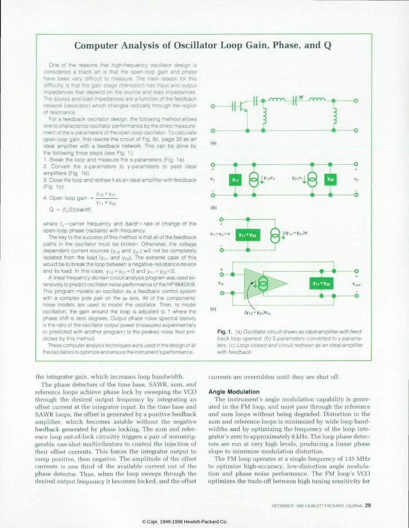
Computer Analysis of Oscillator Loop Gain, Phase, and Q
One o f the reasons tha t h igh - f requency osc i l l a to r des ign i s cons ide red a b l ack a r t i s t ha t t he open - l oop ga in and phase have been very d i f f i cu l t to measure . The ma in reason fo r th i s d i f f icu l ty is that the gain stage ( t ransistor) has input and output impedances tha t depend on the source and load impedances . The source and load impedances are a funct ion of the feedback network ( resonator) which changes radical ly through the region of resonance.
For a feedback osci l la tor design, the fo l lowing method al lows one to characterize osci l lator performance by the direct measure ment of the s-parameters of the open-loop oscil lator. To calculate open-loop gain, f i rst rewri te the circui t of Fig. 9c, page 30 as an idea l amp l i f i e r w i th a feedback ne twork . Th is can be done by the fol lowing three steps (see Fig. 1): 1. Break the loop and measure the s-parameters (Fig. 1a) . 2 C o n v e r t t h e s - p a r a m e t e r s t o y - p a r a m e t e r s t o y i e l d i d e a l ampli f iers (Fig. 1b). 3. Close the loop and redraw it as an ideal amplif ier with feedback (Fig. 1c).
V 1 2 + V 2 1 4 . Open l oop ga in = V 1 1 + V 2 2
Q =
where f0 = carrier frequency and d<¿>/df = rate of change of the open- loop phase ( rad ians) wi th f requency.
The key to the success of this method is that all of the feedback paths in the osc i l la to r must be broken. Otherwise , the vo l tage dependent current sources (y12 and y21) wi l l not be completely iso lated f rom the load (y- , - , and y22) . The extreme case of th is would be to break the loop between a negative-resistance device and its load. In this case, y12 + V2i =° ancl V-n +Y22<0
A linear frequency-domain circuit analysis program was used ex tensively to predict oscillator noise performance of the HP 8642A/B. This program models an osci l lator as a feedback control system wi th a complex pole pai r on the j io ax is . A l l o f the components ' no ise models are used to model the osc i l la tor . Then, to model osc i l la t ion, the gain around the loop is ad justed to 1 where the phase shif t is zero degrees. Output phase noise spectral density is the ratio of the oscillator output power (measured experimentally or predicted with another program) to the peaked noise f loor pre dicted by this method.
These computer analysis techniques were used in the design of all the oscillators to optimize and ensure the instrument's performance.
x ( y i 2 + V 2 l ) V Â ¡ n
Fig. feed . (a) Oscillator circuit drawn as ideal amplifier with feed back loop opened, (b) S-parameters conver ted to y-parame ters. (c) Loop closed and circuit redrawn as an ideal ampli f ier wi th feedback.
the integrator gain, which increases loop bandwidth. The phase detectors of the time base, SAWR, sum, and
reference loops achieve phase lock by sweeping the VCO through the desired output frequency by integrating an offset current at the integrator input. In the time base and SAWR loops, the offset is generated by a positive feedback amplifier, which becomes astable without the negative feedback generated by phase locking. The sum and refer ence loop out-of-lock circuitry triggers a pair of nonretrig- gerable one-shot multivibrators to control the injection of their offset currents. This forces the integrator output to ramp positive, then negative. The amplitude of the offset currents is one third of the available current out of the phase detector. Thus, when the loop sweeps through the desired output frequency it becomes locked, and the offset
currents are overridden until they are shut off.
Angle Modulat ion The instrument's angle modulation capability is gener
ated in the FM loop, and must pass through the reference and sum loops without being degraded. Distortion in the sum and reference loops is minimized by wide loop band- widths and by optimizing the frequency of the loop inte grator's zero to approximately 8 kHz. The loop phase detec tors are run at very high levels, producing a linear phase slope to minimize modulation distortion.
The FM loop operates at a single frequency of 135 MHz to optimize high-accuracy, low-distortion angle modula tion and phase noise performance. The FM loop's VCO optimizes the trade-off between high tuning sensitivity for
DECEMBER 1985 HEWLETT-PACKARD JOURNAL 29
© Copr. 1949-1998 Hewlett-Packard Co.

low-distortion FM and low sensitivity to prevent modula tion by audio-path noise. The FM loop VCO typically pro duces less than -55 dB (0.18%) distortion for 100-kHz de viation. Switching into low-distortion mode further reduces FM distortion. This mode employs a shaper using a JFET in its saturated, constant-resistance region to predistort the modulating signal, cancelling the distortion generated in the VCO. At a small cost to the FM loop's noise perfor mance, switching into low-distortion mode improves FM distortion to typically better than -80 dB (0.01%) at a 1-kHz rate and 100-kHz deviation. Performance degrades slightly with increased modulation frequency, primarily because of limitations in the audio path.
FM distortion from nonlinear operation of the loop's phase/frequency detector at low-rate, large-deviation FM is reduced by limiting the phase detector's deviation to ±1 radian. Because the phase detector operates at 1/1080 of the VCO frequency, the multiplying phase-locked loop pro duces a corresponding ± 1080-radian deviation at the loop's output.
Modulation is applied at two points in the loop. These are the phase detector output and the VCO input (see Fig. 4). Signals summed with the phase detector output cause phase modulation at the loop output. However, there is a low-pass characteristic between the voltage applied and the phase modulation obtained. The 3-dB point of the low- pass response is the 3-dB loop bandwidth, approximately 100 Hz. Consequently, without a crossover network, phase modulation is possible only from dc to 100 Hz.
Frequency modulation is obtained by summing a signal with the loop filter output and applying it to the VCO input. The frequency modulation obtained is rolled off by the phase-locked loop inside the loop bandwidth. Since the FM loop bandwidth is approximately 100 Hz, without a crossover network, frequency modulation would be pos sible only for modulation rates greater than 100 Hz.
The FM and PM crossover networks rely on the derivative relationship between instantaneous frequency and phase:
f(t) = d<A(t)/dt
4>[t) = Jf(t)dt.
The phase modulation crossover network is a differentiator whose output,
= dVin(t)/dt,
is applied to the VCO input. VPMX is the phase modulation crossover output voltage. The resulting FM occurs outside the loop bandwidth and is proportional to VPMX(t), that is,
f ( t ) = C
where Cj is a constant. This is equivalent to phase modula tion of
m =
The phase modulation crossover network allows 100 radians of phase deviation from dc to 15 kHz (3-dB bandwidth).
The FM crossover network is an integrator. The FM cross over output voltage is
= ;vin(t)dt. This signal is summed with the phase detector output and causes phase modulation proportional to VFMX(t), i.e.,
= c2vF (t)
where C2 is a constant. This phase modulation occurs in side the loop bandwidth and is equivalent to frequency modulation of
Af(t) = d[C2VFMX(t)]/dt
= d[CJVln(t)dt]/dt
= C2Vin(t).
The FM crossover circuit has two modes of operation. In normal operation the crossover network approximates an ideal integrator down to 3 Hz and provides better than 5% flatness from 20 Hz to 100 kHz. The crossover feedback is altered in low-rate-FM mode and the integrator approx imation is extended to 0.3 Hz. The low-rate-FM mode al lows phase-locked FM with a 3-dB bandwidth of 0.4 Hz to 200 kHz, at the expense of increased settling time in response to changes in the modulating signal.
For extremely low-rate FM or for direct, external fre quency control of the HP 8642 A/B, dcFM mode is available. In dcFM mode, the FM VCO is not phase-locked. The FM
(b)
-Xa-
* Hl·
T F i g . 9 . ( a ) H a r t l e y o s c i l l a t o r . ( b ) H a r t l e y o s c i l l a t o r r e d r a w n . (c) Modif ied Hart ley osci l lator.
30 HEWLETT-PACKARD JOURNAL DECEMBER 1985
© Copr. 1949-1998 Hewlett-Packard Co.
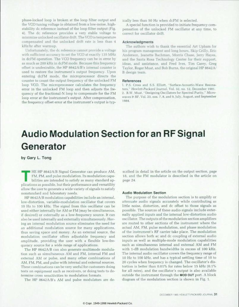
phase-locked loop is broken at the loop filter output and the VCO tuning voltage is obtained from a low-noise, high- stability dc reference instead of the loop filter output (Fig. 4). The dc reference provides a ven" stable voltage to minimize unlocked oscillator drift. The VCO is temperature compensated and the unlocked drift rate is less than 4 kHzhr after warmup.
Unfortunately, the dc reference cannot provide a voltage with sufficient accuracy to set the VCO at exactly 135 MHz in dcFM operation. The VCO frequency can be in error by as much as 200 kHz in dcFM mode. Because this frequency offset is undesirable, the HP 8642A/B's internal counter is used to restore the instrument's output frequency. Upon entering dcFM mode, the microprocessor directs the counter to count the output frequency of the unlocked FM loop VCO. The microprocessor calculates the frequency error in the unlocked FM loop and then adjusts the fre quency of the fractional-N loop to compensate for the FM loop error at the instrument's output. After compensation, the frequency offset error at the instrument's output is typ
ically less than 50 Hz when dcFM is selected. A special function is provided to initiate frequency com
pensation of the unlocked FM oscillator at any time, to correct for oscillator drift.
Acknowledgments The authors wish to thank the essential Art Upham for
his program management and long hours. Skip Crilly. Eric Anderson. Jeanette Bachman, Morris Chase, Jerry Hayes, and the Santa Rosa Technology Center for their support, ideas, and assistance, and Fred Ivés, Tim Carey, Greg Taylor, Roger Muat, and Bob Burns, the original HP 8642A B design team.
References 1. P.S. Cross and S.S. Elliott, "Surface-Acoustic-Wave Resona tors," Hewlett-Packard Journal, Vol. 32, no. 12, December 1981. 2. R.VV. Muat, "Designing Oscillators for Spectral Purity," Micro waves 6- RF, Vol. 23, nos. 7, 8, and 9, July, August, and September 1984.
Audio Modulation Section for an RF Signal Generator by Gary L. Tong
THE HP 8642A/B Signal Generator can produce AM, FM, PM, and pulse modulation. Its modulation capa bilities are intended to satisfy as many standard ap
plications as possible, but their performance and versatility allow the user to generate a wide variety of signals to satisfy nonstandard and laboratory needs.
HP 8642 A/B modulation capabilities include an internal, low-distortion, variable-modulation oscillator that covers 10 Hz to 100 kHz. The signal from this oscillator can be used either internally for AM or FM (may be simultaneous, if desired) or externally as a low-frequency source. It can also be used internally and externally simultaneously. Hav ing an internal modulation source eliminates the need for an additional modulation source for many applications, thus saving space and money. As an external source, the modulation oscillator offers adjustable frequency and amplitude, providing the user with a flexible low-fre quency source for a wide range of applications.
The HP 8642A/B can also generate multimode modula tion such as simultaneous AM and FM, internal FM and external AM or pulse, and many other combinations of AM, FM, PM, and pulse with internal and external sources. These combinations can be very useful for customers doing tests on equipment such as receivers, or doing tests to de termine cross sensitivities to modulation formats.
The HP 8642A/B's AM and pulse modulators are de
scribed in detail in the article on the output section, page 18, and the FM modulator is described in the article on page 24.
Audio Modulat ion Sect ion The purpose of the modulation section is to amplify or
attenuate audio signals accurately while contributing as little noise, distortion, and dc offset to those signals as possible. The sources of these audio signals include exter nally applied inputs and the internal low-distortion audio oscillator. The outputs of the modulation section amplifiers are routed to other sections of the instrument where the actual AM, FM, pulse modulation, and phase modulation of the instrument's RF carrier take place. The modulation section allows both ac and dc coupling of external audio inputs as well as multiple-mode modulation capabilities such as simultaneous internal and external AM and FM with 1-dB modulation bandwidths in excess of 100 kHz. The internal audio oscillator covers the frequency range of 10 Hz to 100 kHz, and has a typical settling time of 10 to 20 cycles when frequency is changed. The oscillator's dis tortion is better than 0.01% for rates below 15 kHz (0.1% for all rates), and the oscillator's output is also available outside the instrument through the MOD OUT port. A block diagram of the modulation section is shown in Fig. 1.
DECEMBER 1985 HEWLETT-PACKARD JOURNAL 31
© Copr. 1949-1998 Hewlett-Packard Co.
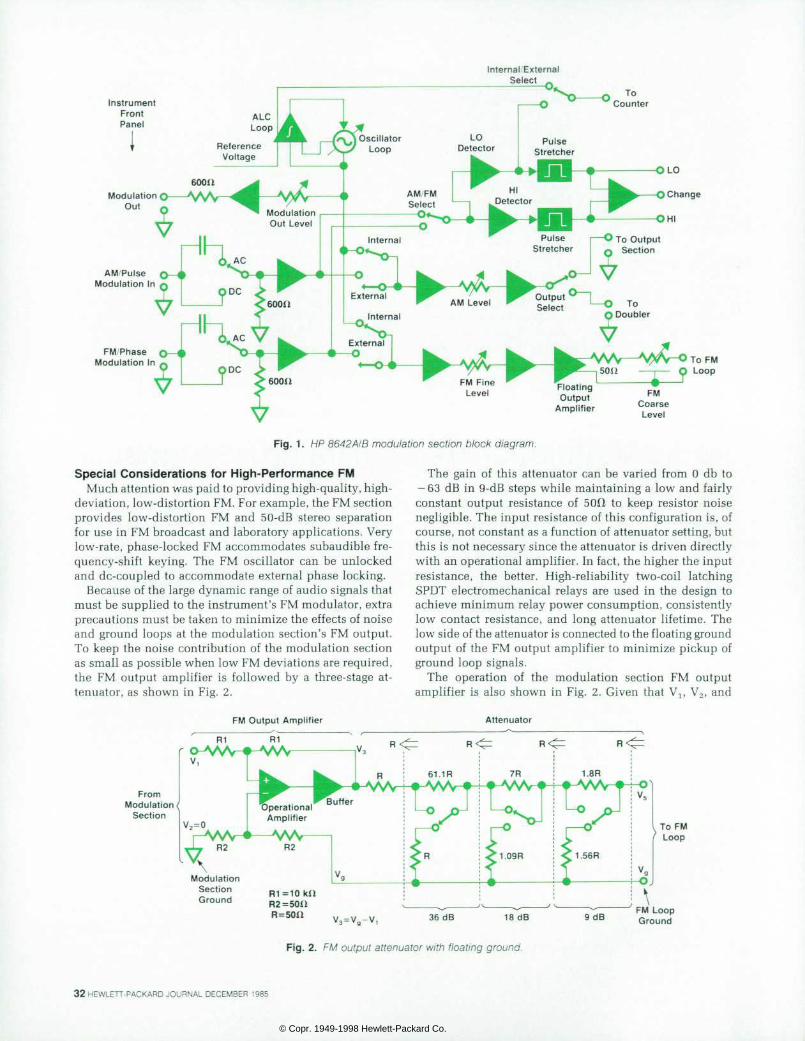
Internal/External Select
Change
AM Pulse Modula t ion In Q
FM Phase Modulation In
Floating Output
Amplifier FM
Coarse Level
Fig. 1. HP 8642 A/ B modulat ion sect ion block diagram.
Special Considerat ions for High-Performance FM Much attention was paid to providing high-quality, high-
deviation, low-distortion FM. For example, the FM section provides low-distortion FM and 50-dB stereo separation for use in FM broadcast and laboratory applications. Very low-rate, phase-locked FM accommodates subaudible fre quency-shift keying. The FM oscillator can be unlocked and de-coupled to accommodate external phase locking.
Because of the large dynamic range of audio signals that must be supplied to the instrument's FM modulator, extra precautions must be taken to minimize the effects of noise and ground loops at the modulation section's FM output. To keep the noise contribution of the modulation section as small as possible when low FM deviations are required, the FM output amplifier is followed by a three-stage at tenuator, as shown in Fig. 2.
FM Output Ampl i f ier
From Modulation (
Section
The gain of this attenuator can be varied from 0 db to — 63 dB in 9-dB steps while maintaining a low and fairly constant output resistance of 50Ã1 to keep resistor noise negligible. The input resistance of this configuration is, of course, not constant as a function of attenuator setting, but this is not necessary since the attenuator is driven directly with an operational amplifier. In fact, the higher the input resistance, the better. High-reliability two-coil latching SPDT electromechanical relays are used in the design to achieve minimum relay power consumption, consistently low contact resistance, and long attenuator lifetime. The low side of the attenuator is connected to the floating ground output of the FM output amplifier to minimize pickup of ground loop signals.
The operation of the modulation section FM output amplifier is also shown in Fig. 2. Given that Va, V2, and
Attenuator
36 dB 18 dB V 3 = V g - V ,
Fig. 2 . FM output a t tenuator wi th f loat ing ground
9 dB FM Loop Ground
32 HEWLETT-PACKARD JOURNAL DECEMBER 1985
© Copr. 1949-1998 Hewlett-Packard Co.
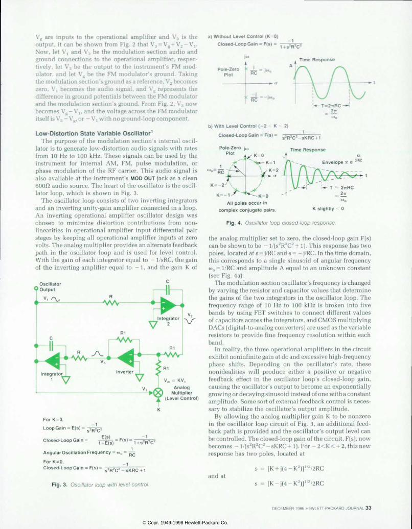
Closed-Loop Gain = F(s) =
Pole-Zero Plot RC
Vg are inputs to the operational amplifier and V3 is the a) Without Level Control (K=0) output, it can be shown from Fig. 2 that V3 = Vg+ V2 — Vr Now, let Y! and V2 be the modulation section audio and ground connections to the operational amplifier, respec tively, let V3 be the output to the instrument's FM mod ulator, and let Vg be the FM modulator's ground. Taking the modulation section's ground as a reference, V, becomes zero, Vj becomes the audio signal, and Vg represents the difference in ground potentials between the FM modulator and the modulation section's ground. From Fig. 2, V3 now becomes Vg — V1, and the voltage across the FM modulator itself is V3 - Vg, or - Vj with no ground-loop component.
-1 1+s2R2C2
T ime Response
RC
* - t
Low-Distortion State Variable Oscil lator1 The purpose of the modulation section's internal oscil
lator is to generate low-distortion audio signals with rates from 10 Hz to 100 kHz. These signals can be used by the instrument for internal AM, FM, pulse modulation, or phase modulation of the RF carrier. This audio signal is also available at the instrument's MOD OUT jack as a clean 600fi audio source. The heart of the oscillator is the oscil lator loop, which is shown in Fig. 3.
The oscillator loop consists of two inverting integrators and an inverting unity-gain amplifier connected in a loop. An inverting operational amplifier oscillator design was chosen to minimize distortion contributions from non- linearities in operational amplifier input differential pair stages by keeping all operational amplifier inputs at zero volts. The analog multiplier provides an alternate feedback path in the oscillator loop and is used for level control. With the gain of each integrator equal to - 1/sRC, the gain of the inverting amplifier equal to -1, and the gain K of
Oscillator 0 O u t p u t
b ) W i t h L e v e l C o n t r o l ( - 2 K 2 )
V m = K V , Analog
Multiplier (Level Control)
For K=0 ,
Loop Gain = E(s) = -
Closed-Loop Gain = 1+s2R2C2
Angular Oscillation Frequency = i»0 = —
-1 F o r K * 0 , Closed-Loop Gain = F(s) = !C2-sKRC+1
Fig. 3. Osci l lator loop wi th level control .
Closed-Loop Gain = F(s) =
Pole-Zero ¡¡a
- 1 s 2 R 2 C 2 - s K R C + 1
T ime Response
All poles occur in c o m p l e x c o n j u g a t e p a i r s . K s l i g h t l y 0
Fig. 4 . Osc i l la tor loop c losed- loop response.
the analog multiplier set to zero, the closed-loop gain F(s) can be shown to be — l/(s2R2C2 + 1). This response has two poles, located at s = j/RC and s = — j/RC. In the time domain, this corresponds to a single sinusoid of angular frequency co0 = 1/RC and amplitude A equal to an unknown constant (see Fig. 4a).
The modulation section oscillator's frequency is changed by varying the resistor and capacitor values that determine the gains of the two integrators in the oscillator loop. The frequency range of 10 Hz to 100 kHz is broken into five bands by using FET switches to connect different values of capacitors across the integrators, and CMOS multiplying DACs (digital-to-analog converters) are used as the variable resistors to provide fine frequency resolution within each band.
In reality, the three operational amplifiers in the circuit exhibit noninfinite gain at dc and excessive high-frequency phase shifts. Depending on the oscillator's rate, these nonidealities will produce either a positive or negative feedback effect in the oscillator loop's closed-loop gain, causing the oscillator's output to become an exponentially growing or decaying sinusoid instead of one with a constant amplitude. Some sort of external feedback control is neces sary to stabilize the oscillator's output amplitude.
By allowing the analog multiplier gain K to be nonzero in the oscillator loop circuit of Fig. 3, an additional feed back path is provided and the oscillator's output level can be controlled. The closed-loop gain of the circuit, F(s), now becomes -l/(s2R2C2-sKRC + l). For -2<K< + 2,thisnew response has two poles, located at
and at s = [K + j(4-K2)]1/2/2RC
s = [K-j(4-K2)]1/2/2RC
DECEMBER 1985 HEWLETT-PACKARD JOURNAL 33
© Copr. 1949-1998 Hewlett-Packard Co.
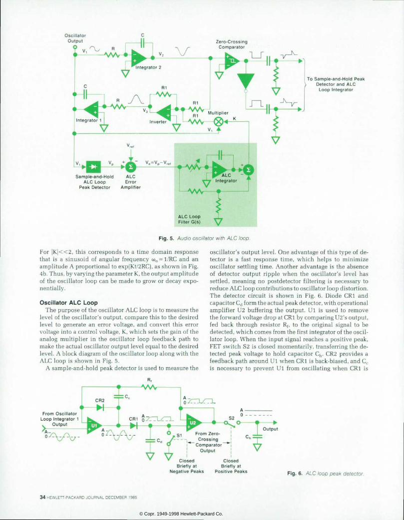
Oscillator Output Zero-Crossing
Comparator
To Sample-and-Hold Peak ) D e t e c t o r a n d A L C
Loop Integrator
S a m p l e - a n d - H o l d A L C A L C L o o p E r r o r
P e a k D e t e c t o r A m p l i f i e r
ALC Loop Filter G(s)
Fig. 5 . Audio osc i l la tor w i th ALC loop.
For |K|«2, this corresponds to a time domain response that is a sinusoid of angular frequency ta0 = 1/RC and an amplitude A proportional to exp(Kt/2RC), as shown in Fig. 4b. Thus, by varying the parameter K, the output amplitude of the oscillator loop can be made to grow or decay expo nentially.
Osci l lator ALC Loop The purpose of the oscillator ALC loop is to measure the
level of the oscillator's output, compare this to the desired level to generate an error voltage, and convert this error voltage into a control voltage, K, which sets the gain of the analog multiplier in the oscillator loop feedback path to make the actual oscillator output level equal to the desired level. A block diagram of the oscillator loop along with the ALC loop is shown in Fig. 5.
A sample-and-hold peak detector is used to measure the
oscillator's output level. One advantage of this type of de tector is a fast response time, which helps to minimize oscillator settling time. Another advantage is the absence of detector output ripple when the oscillator's level has settled, meaning no postdetector filtering is necessary to reduce ALC loop contributions to oscillator loop distortion. The detector circuit is shown in Fig. 6. Diode CRl and capacitor Cd form the actual peak detector, with operational amplifier U2 buffering the output. Ul is used to remove the forward voltage drop at CRl by comparing U2's output, fed back through resistor Rf, to the original signal to be detected, which comes from the first integrator of the oscil lator loop. When the input signal reaches a positive peak, FET switch S2 is closed momentarily, transferring the de tected peak voltage to hold capacitor Ch. CR2 provides a feedback path around Ul when CRl is back-biased, and Cc is necessary to prevent Ul from oscillating when CRl is
From Oscil lator Loop Integrator 1 K O u t p u t ? i
~ S 1 F r o m Z e r o - â € ” ! C r o s s i n g
Comparator Output
C l o s e d C l o s e d B r i e f l y a t B r i e f l y a t
N e g a t i v e P e a k s P o s i t i v e P e a k s
-t — > Outpu
Fig . 6 . ALC loop peak de tec to r .
34 HEWLETT-PACKARD JOURNAL DECEMBER 1985
© Copr. 1949-1998 Hewlett-Packard Co.
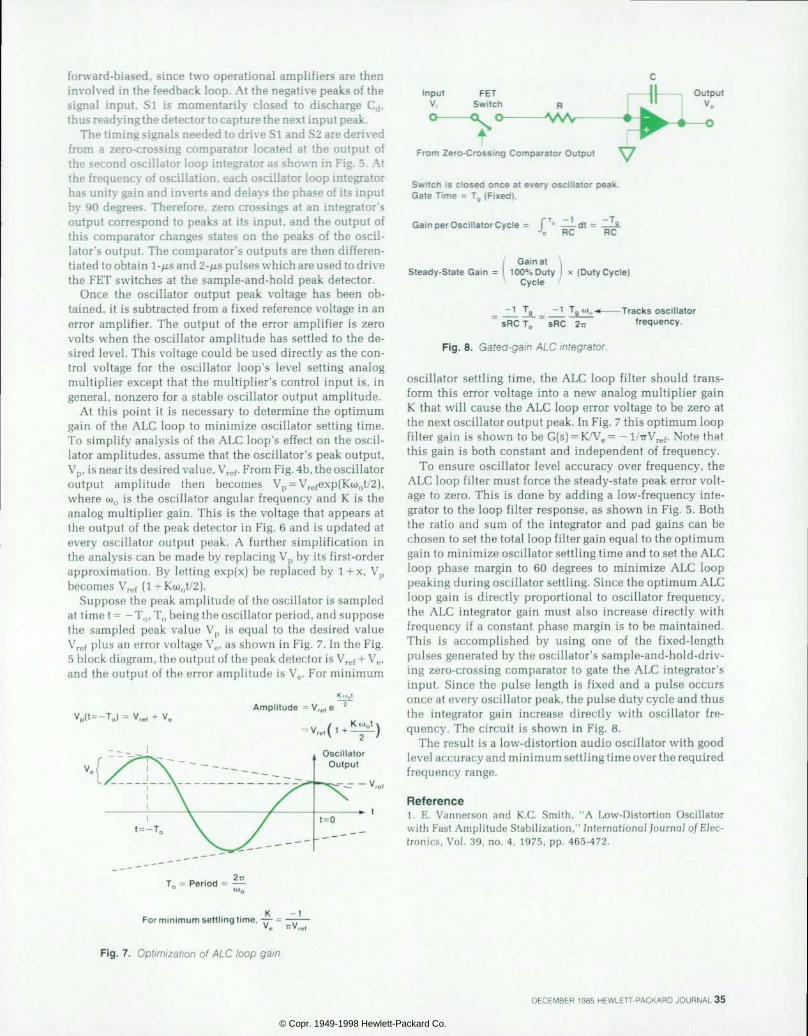
forward-biased, since two operational amplifiers are then involved in the feedback loop. At the negative peaks of the signal input. SI is momentarily closed to discharge C¿, thus readying the detector to capture the next input peak.
The timing signals needed to drive Si and S2 are derived from a zero-crossing comparator located at the output of the second oscillator loop integrator as shown in Fig. 5. At the frequency of oscillation, each oscillator loop integrator has unity gain and inverts and delays the phase of its input by 90 degrees. Therefore, zero crossings at an integrator's output correspond to peaks at its input, and the output of this comparator changes states on the peaks of the oscil lator's output. The comparator's outputs are then differen tiated to obtain 1-fj.s and 2-/xs pulses which are used to drive the FET switches at the sample-and-hold peak detector.
Once the oscillator output peak voltage has been ob tained, it is subtracted from a fixed reference voltage in an error amplifier. The output of the error amplifier is zero volts when the oscillator amplitude has settled to the de sired level. This voltage could be used directly as the con trol voltage for the oscillator loop's level setting analog multiplier except that the multiplier's control input is, in general, nonzero for a stable oscillator output amplitude.
At this point it is necessary to determine the optimum gain of the ALC loop to minimize oscillator setting time. To simplify analysis of the ALC loop's effect on the oscil lator amplitudes, assume that the oscillator's peak output, Vp, is near its desired value, Vre[. From Fig. 4b, the oscillator output amplitude then becomes Vp = Vrefexp(Ku>0t/2), where co0 is the oscillator angular frequency and K is the analog multiplier gain. This is the voltage that appears at the output of the peak detector in Fig. 6 and is updated at every oscillator output peak. A further simplification in the analysis can be made by replacing Vp by its first-order approximation. By letting exp(x) be replaced by 1 + x, Vp becomes Vref (l + Kco0t/2).
Suppose the peak amplitude of the oscillator is sampled at time t = - T0, T0 being the oscillator period, and suppose the sampled peak value Vp is equal to the desired value Vref plus an error voltage Ve, as shown in Fig. 7. In the Fig. 5 block diagram, the output of the peak detector is Vref + Ve, and the output of the error amplitude is Ve. For minimum
Amplitude = Vre, e
Output
From Zero-Crossing Comparator Output
Switch is closed once at every osci l lator peak. Gate Time = Tg (Fixed) .
G a i n p e r O s c i l l a t o r C y c l e = J ~ T ' â € ” d t = l l i o R C R C
Gain at Steady-State Gain = I 100% Duty
Cycle x (Duty Cycle)
S R C T 0 S R C 2 - n
Fig . 8 . Gated-ga in ALC in tegrator .
-Tracks osci l la tor frequency.
t = - T ,
oscillator settling time, the ALC loop filter should trans form this error voltage into a new analog multiplier gain K that will cause the ALC loop error voltage to be zero at the next oscillator output peak. In Fig. 7 this optimum loop filter gain is shown to be G(s) = K/Ve = - l/irVref. Note that this gain is both constant and independent of frequency.
To ensure oscillator level accuracy over frequency, the ALC loop filter must force the steady-state peak error volt age to zero. This is done by adding a low-frequency inte grator to the loop filter response, as shown in Fig. 5. Both the ratio and sum of the integrator and pad gains can be chosen to set the total loop filter gain equal to the optimum gain to minimize oscillator settling time and to set the ALC loop phase margin to 60 degrees to minimize ALC loop peaking during oscillator settling. Since the optimum ALC loop gain is directly proportional to oscillator frequency, the ALC integrator gain must also increase directly with frequency if a constant phase margin is to be maintained. This is accomplished by using one of the fixed-length pulses generated by the oscillator's sample-and-hold-driv- ing zero-crossing comparator to gate the ALC integrator's input. Since the pulse length is fixed and a pulse occurs once at every oscillator peak, the pulse duty cycle and thus the integrator gain increase directly with oscillator fre quency. The circuit is shown in Fig. 8.
The result is a low-distortion audio oscillator with good level accuracy and minimum settling time over the required frequency range.
Reference 1. E. Vannerson and K.C. Smith, "A Low-Distortion Oscillator with of Amplitude Stabilization," international Journal of Elec tronics, Vol. 39, no. 4, 1975, pp. 465-472.
T0 = Per iod = —
K â € ” 1 For minimum settling time, — = V e "
Fig. 7 . Opt imizat ion o f ALC loop ga in .
DECEMBER 1985 HEWLETT-PACKARD JOURNAL 35
© Copr. 1949-1998 Hewlett-Packard Co.
H E W L E T T - P A C K A R D J O U R N A L Volume 36 January 1985 th rough December 1985 naex Hewlet t -Packard Company, 3000 Hanover Street , Palo Al to, Cal i forn ia 94304 U.S.A.
Hewlett-Packard Central Mailing Dept., P.O. Box 529, Startbaan 1 6, 1 1 80 AM Amstelveen, The Netherlands Hewlet t -Packard (Canada) L td. , 6877 Goreway Dr ive, Miss issauga, Ontar io L4V 1M8 Canada Yokogawa-Hewlet t -Packard Ltd. , Suginami-ku, Tokyo 168 Japan
PART 1: Chrono log ica l Index January 1985 Optical Stimulus and Receivers for Parametric Testing in Fiber
Optics, Achim Eckert and Wolfgang Schmid Handling Fiber Optic Components A Precise, Programmable 850-nm Optical Signal Source, Wolfgang
Schmid, Bernhard Fiade, Klaus Hoeing, and Rainer Eggert Laser Safety Practices A Versatile, Programmable Optical Pulse Power Meter, Werner
Berkei, Hans Huning, VoÃker EberÃe, Josef Becker, Bernd Maisen- bacher, Wilfried PJess, and Michael Coder
An Opt ica l Receiver for 550 to 950 nm, MichaeJ Fle ischer- Reumann, Emmerich MiiJler, and Gerd Kof/mane
Optical Standards, Werner Berkei and Joachim Vobis
February 1985 HP TechWriter: Illustrated Documents for Engineers, Elaine C.
Regeison and Roy E. Anderson HP TechWriter Security Magnetostatic-Wave Devices for Microwave Signal Processing,
Waguih S. Ishak and Kok-Wai Chang Magnetic Resonance and YIG-Sphere Devices Spin Waves and Magnetostatic Waves Disc Caching in the System Processing Units of the HP 3000 Family
of Computers, John R. Busch and Alan /. Kondoff Glossary Disc Cache Performance Tools The MPE-IV Kernel
March 1985 HP Maintenance Management: A New Approach to Software Cus
tomer Solutions, Joseph L. Malin and Irving Bunton, Jr.
The Need for Plant Maintenance Development of a High-Performance, Half-Inch Tape Drive, Hoyle
L. Curtis and Richard T. Turley LSI Simplifies Tape Drive Electronic Design System Integration Write and Read Recovery Systems for a Half-Inch Tape Drive,
Wayne T. Gregory Digital Formatting and Control Electronics for Half-Inch Tape Data
Storage, Jimmy L. Shafer Streaming Tape Drive Hardware Design, John W. Dong, David /.
Van Maren, and Robert D. Emmerich Firmware for a Streaming Tape Drive, David W. Ruska, Virgil K.
Russon, Brad/red W. Gulp, Alan /. Richards, and John A. Ruf
Low-Cost, Highly Reliable Tape Backup for Winchester Disc Drives, John C. Becker, Donald A. DiTommaso, and Sterling /. Mortensen
A Design Methodology for Today's Customers Tape/Disc Controller Serves Integrated Peripherals, Craig L.
Miller and Mark L. Gembarowski
Cartridge Tape Data Integrity Ensured at Five Levels, K. Douglas Gennetten
Controlling the Head/Tape Interface, Walter L. Auyer, Charles H. McConica, David /. Schmeling, and Mark E. Wanger
Software Methodology Preserves Consistency and Creativity, Mark L. Gembarowski
April 1985 A Low-Cost, Compact, Block-Mode Computer Terminal, Jean-
Louis Chapuis and Michele Prieur A Reliable, Low-Cost Keyboard Interface Mechanical Design of a Low-Cost Terminal, Michel Cauzid VLSI Design in the HP 2392A Terminal, Jean-Jacques Simon A Fast Gate Array Companion for a CRT Controller How to Scroll Smoothly Fully Automated Production of Display Terminal Printed Circuit
Assemblies, Christian-Marcel DuJphy A Low-Cost, Reliable Analog Video Display Terminal Design,
Rene Martinelli and Jean Yves Chatron An Intelligent Plotter for High-Throughput, Unattended Opera
tion, Martin L. Stone, Peter L. Ma, Jeffery W. Groenke, and Todd L. Russell
Low-Mass, Low-Cost Pen-Lift Mechanism for High-Speed Plotting, Tammy V. Herr and Hatem E. Mosta/a
The HP 7550A X-Y Servo: State-of-the-Art Performance on a Budget, by David C. Tribolet, Kenneth A. Regas, and Thomas J. Halpenny
Fi rmware Provides Simple and Powerful P lo t ter Opera t ion , Thomas J. Halpenny
May 1985 History of Thinkjet Printhead Development, Niels Nielsen Mass-Producing Thermal Ink-Jet Printheads Preventing Hydraulic Crosstalk An Inexpensive, Portable Ink-Jet Printer Family, Cheryl V. Katen
and Thomas R. Braun Alignment of Bidirectional Text Printhead Interconnect Custom VLSI Microprocessor System Home Switch Design Development of the Thin-Film Structure for the Thinkjet Printhead,
Eldurkar V. Bhaskar and J. Stephen Aden Where the Ink Hits the Paper. . . The Thinkjet Orifice Plate: A Part with Many Functions, Gary L.
Siewell, William R. Boucher, and PauJ H. McClelland Electroforming Viewpoints — Managing the Development of a New Technology,
Frank L. Cloutier Thermodynamics and Hydrodynamics of Thermal Ink Jets, Ross
R. Allen, John D. Meyer, and William R. Knight
36 HEWLETT-PACKARD JOURNAL DECEMBER 1985
© Copr. 1949-1998 Hewlett-Packard Co.
June 1985 A New Family of Dot Matrix Line Printers. Bryce E. Jeppsen Design for Reliability in the HP 256X Family of Line Printers Dot Matrix Printbar Design and Manufacturing, John S. Craven Shuttle System and Packaging of a Low-Cost, High-Reliability.
300-lpm Line Printer, by Jeffrey M. Lantz and Ben B. Tyson Mechanical Design of a Family of High-Speed Impact Line Printers,
George V. McIJvaine, Stephen L. Testardi, Daniel D. Wheeler, and Peter Gysling
Computer Modeling of a Paper Drive Mechanism Resonance Search Technique Cost-Effective, Versatile Line Printer Electronics and Firmware,
Philip Gordon, PhiJJip R. Luque, and Donald K. Wadley Vector Graphics for Dot Matrix Printers Printer Command Language Provides Feature Set Standard for HP
Printers, Ernest F. Covelli, Von L. Hansen, and David L. Price Native Language Support for Computer Systems, Jonathan E. Bale
and Harry E. Kellogg Native Language Collating Sequences for Europe
July 1985 A Protocol Analyzer for EDP Centers and Field Service, Aileen
C. Appleyard, Roger W. Ruhnow, William Grant Grovenburg, and Wayne M. Angevine
How Protocol Analysis Can Help Protocol Analyzer Software Development Simple Architecture Provides High Performance for Protocol
Analysis, Stephen H. Witt and Roger W. Ruhnow Protocol Analyzer Power Supply Design Protocol Analyzer Mechanical Design Making a Protocol Analyzer Producible and Serviceable Serial Data Acquisition and Simulation for a High-Speed Protocol
Analyzer, Mark D. Keisiing, Dorothy/. Yackle, David B. Kariin, and Elizabeth Gates Moore
A Low-Cost, Portable Field Service Protocol Analyzer, Vonn L. Block, Alan Delwiche, Chris L. Odell, and Stephen B. Tursich
Remote Monitoring and Control of Semiconductor Processing, Wesley H. Higaki
SECS
August 1985 Beyond RISC: High-Precision Architecture, /oel S. Birnbaum and
William S. Worley, Jr.
Architecture Genealogy Development of a Two-Channel Frequency Synthesizer, Michael
B. Aken and William M. Spaulding Discrete Sweep Two-Channel Synthesizer Phase Calibration Applications of a Two-Channel Synthesizer, Michael B. Aken Measuring Intermodulation Distortion with a Two-Channel Syn
thesizer Synthesizer Firmware for User Interface and Instrument Control,
David A. Bartle and (Catherine F. Potter A High-Level Active Mixer, William M. Spaulding Automated Test Data Collection for 1C Manufacturing, Reed I. White EA-10 Data Analysis System
September 1985 VLSI Delivers Low-Cost, Compact HP 3000 Computer System,
/ames H. Holl and Frank E. La Fetra, Jr. High-Volume Test Strategy Simplicity in a Microcoded Computer Architecture, Frederic C.
Amerson Using a Translator for Creating Readable Microcode Booting 64-Bit WCS Words from a 32-Bit-Wide ROM Word Simulation Ensures Working First-Pass VLSI Computer System,
PÃ tria G. Alvarez, Greg L. Gilliom, John R. Obermeyer, Paul L. Rogers, and Malcolm E. Woodward
Creative Ways to Obtain Computer System Debug Tools, William M. Pam'sh. Eric B. Decker, and Edwin G. Wong
The Role of a Programmable Breakpoint Board Virtual Microcode Memory New Cardiograph Family with ECG Analysis Capability, Robert
H. Banta, /r., Peter H. Donvard, and Steven A. Scampini ECG Storage and Transmission Artifact Indication Computer-Aided ECG Analysis, John C. Doue and Anthony G.
Vallance ECG Criteria Language Pediatric Criteria
October 1985 A Multitasking Personal Computer System for the Technical Pro
fessional, Tim /. Williams and Nelson A. Mills Electronics System for a Transpor table Computer , David L.
Kepler and James A. Espeland Custom Graphics Processor Unit for the Integral PC, Dean M. Heath High-Quality Electroluminescent Display for a Personal Worksta
tion, Marvin L. Higgins Mechanical Design of the Integral PC: Not Just a Desktop Computer
with a Handle, Thomas A. Pearo Reducing Glare with Circular Polarizers A UNIX Operating System Adapted for a Technical Personal Com
puter, Ray M. Fajardo, Andrew L. Rood, James R. Andreas, and Robert C. Cline
A Friendly UNIX Operating System User Interface, /on A. Brewster, Karen S. Helt, and James N. Phillips
Personal Applications Manager Data Communications Printer and Plotter Drivers
November 1985 Thin-Film Memory Disc Development, James E. Op/er, Bruce F.
Spenner, Bangalore R. Natarajan, Richard A. Baugh, Edward S. Murdock, Charles C. Morehouse, and David /. Bromley
M-H Loop Measurements A Laser Particle Scanner Dynamic Testing of Thin-Film Magnetic Recording Discs, John
Hodges, Keith S. Roskelley, and Dennis R. Edson In-Line Sputtering Deposition System for Thin-Film Disc Fabrication,
George A. Drennan, Robert /. Lawton, and Michael B. /acobson Thin-Film Disc Reliability — the Conservative Approach, Clifford
K. Day, C. Girvin Harkins, Stephen P. Howe, and Paul Poorman Manufacturing Thin-Film Discs, Glenn E. Moore, Jr., Richard S.
Seymour, and Darrel R. Bloomquist Thin-Film Discs: Magnetic, Electrical, and Mechanical Design,
Michael C. Allyn, Peter R. Goglia, and Scott R. Smay
December 1985 A High-Performance Signal Generator for RF Communications
Testing, Robert E. Burns User Interface and Internal Controller for an RF Signal Generator,
Albert Einstein Lassiter and Charles R. Kogler Display Design Signal Generator Service Features Maximize Uptime, Michael T.
Wende Electrically Erasable PROM Storage for Calibration Data Internally Modular Signal Generator Mechanical Design, Michael
B. Jewell and Mark W. Johnson Wide-Frequency-Range Signal Generator Output Section Design,
Robert R. Collison, James B. Summers, Marvin W. Wagner, and Bryan D. Ratliff
Signal Generator Frequency Synthesizer Design, Thomas R. Faulkner, Earl C. Herleikson, Ronald /. Mayer, Brian M. Miller, and Mark A. Niemann
Computer Analysis of Oscillator Loop Gain, Phase, and Q Audio Modulation Section for an RF Signal Generator, Gary L. Tong
DECEMBER 1985 HEWLETT-PACKARD JOURNAL 37
© Copr. 1949-1998 Hewlett-Packard Co.
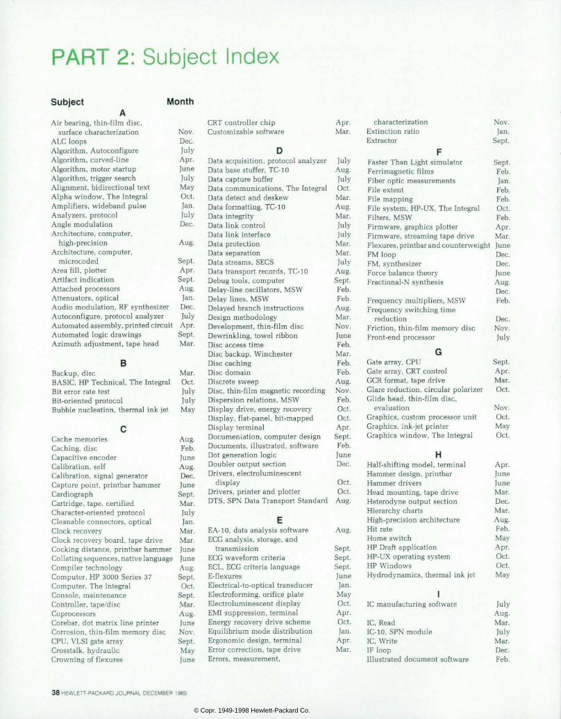
PART 2 : Sub jec t Index
Subject Month
Air bearing, thin-film disc, s u r f a c e c h a r a c t e r i z a t i o n N o v .
A L C l o o p s D e c . A l g o r i t h m , A u t o c o n f i g u r e J u l y A l g o r i t h m , c u r v e d - l i n e A p r . A l g o r i t h m , m o t o r s t a r t u p J u n e A l g o r i t h m , t r i g g e r s e a r c h J u l y A l i g n m e n t , b i d i r e c t i o n a l t e x t M a y A l p h a w i n d o w , T h e I n t e g r a l O c t . A m p l i f i e r s , w i d e b a n d p u l s e J a n . A n a l y z e r s , p r o t o c o l J u l y A n g l e m o d u l a t i o n D e c . Architecture, computer,
h i g h - p r e c i s i o n A u g . Architecture, computer,
m i c r o c o d e d S e p t . A r e a f i l l , p l o t t e r A p r . A r t i f a c t i n d i c a t i o n S e p t . A t t a c h e d p r o c e s s o r s A u g . A t t e n u a t o r s , o p t i c a l J a n . Audio modulation, RF synthesizer Dec. Autoconfigure, protocol analyzer July Automated assembly, printed circuit Apr. A u t o m a t e d l o g i c d r a w i n g s S e p t . Azimuth adjustment, tape head Mar.
B B a c k u p , d i s c M a r . BASIC, HP Technical, The Integral Oct. B i t e r r o r r a t e t e s t J u l y B i t - o r i e n t e d p r o t o c o l J u l y Bubble nucleation, thermal ink jet May
C a c h e m e m o r i e s A u g . C a c h i n g , d i s c F e b . C a p a c i t i v e e n c o d e r J u n e C a l i b r a t i o n , s e l f A u g . Cal ibra t ion , s ignal genera tor Dec. Capture point, printbar hammer June C a r d i o g r a p h S e p t . C a r t r i d g e , t a p e , c e r t i f i e d M a r . C h a r a c t e r - o r i e n t e d p r o t o c o l J u l y Cleanable connectors , opt ical Jan. C l o c k r e c o v e r y M a r . Clock recovery board, tape drive Mar. Cocking distance, printbar hammer June Collating sequences , native language June C o m p i l e r t e c h n o l o g y A u g . Computer, HP 3000 Series 37 Sept. C o m p u t e r , T h e I n t e g r a l O c t . C o n s o l e , m a i n t e n a n c e S e p t . C o n t r o l l e r , t a p e / d i s c M a r . C o p r o c e s s o r s A u g . Corebar, dot matrix line printer June Corrosion, thin-film memory disc Nov. C P U , V L S I g a t e a r r a y S e p t . C r o s s t a l k , h y d r a u l i c M a y C r o w n i n g o f f l e x u r e s J u n e
C R T c o n t r o l l e r c h i p A p r . C u s t o m i z a b l e s o f t w a r e M a r .
Data acquisition, protocol analyzer July D a t a b a s e s t u f f e r , T C - 1 0 A u g . D a t a c a p t u r e b u f f e r J u l y Data communications, The Integral Oct. D a t a d e t e c t a n d d e s k e w M a r . D a t a f o r m a t t i n g , T C - 1 0 A u g . D a t a i n t e g r i t y M a r . D a t a l i n k c o n t r o l J u l y D a t a l i n k i n t e r f a c e J u l y D a t a p r o t e c t i o n M a r . D a t a s e p a r a t i o n M a r . D a t a s t r e a m s , S E C S J u l y Data transport records, TC-10 Aug. D e b u g t o o l s , c o m p u t e r S e p t . De lay- l ine osc i l l a to r s , MSW Feb . D e l a y l i n e s , M S W F e b . De layed b ranch ins t ruc t ions Aug . D e s i g n m e t h o d o l o g y M a r . Deve lopment , t h in - f i lm d i sc Nov . D e w r i n k l i n g , t o w e l r i b b o n J u n e D i s c a c c e s s t i m e F e b . D i s c b a c k u p , W i n c h e s t e r M a r . D i s c c a c h i n g F e b . D i s c d o m a i n F e b . D i s c r e t e s w e e p A u g . Disc, thin-film magnetic recording Nov. D i s p e r s i o n r e l a t i o n s , M S W F e b . Display drive, energy recovery Oct. Display, flat-panel, bit-mapped Oct. D i s p l a y t e r m i n a l A p r . Documentation, computer design Sept. Documents, illustrated, software Feb. D o t g e n e r a t i o n l o g i c J u n e D o u b l e r o u t p u t s e c t i o n D e c . Drivers, electroluminescent
d i s p l a y O c t . D r i v e r s , p r i n t e r a n d p l o t t e r O c t . DTS, SPN Data Transport Standard Aug.
EA-10, data analysis software Aug. ECG analysis, storage, and
t r a n s m i s s i o n S e p t . E C G w a v e f o r m c r i t e r i a S e p t . ECL, ECG cr i te r ia language Sept . E - f l e x u r e s J u n e Electrical-to-optical transducer Jan. E lec t ro forming , o r i f i ce p la te May E l e c t r o l u m i n e s c e n t d i s p l a y O c t . E M I s u p p r e s s i o n , t e r m i n a l A p r . Energy recovery drive scheme Oct. Equil ibrium mode distr ibution Jan. E r g o n o m i c d e s i g n , t e r m i n a l A p r . E r r o r c o r r e c t i o n , t a p e d r i v e M a r . Errors, measurement,
c h a r a c t e r i z a t i o n N o v . E x t i n c t i o n r a t i o J a n . E x t r a c t o r S e p t .
F Fas te r Than Light s imula tor Sept . F e r r i m a g n e t i c f i l m s F e b . F i b e r o p t i c m e a s u r e m e n t s J a n . F i l e e x t e n t F e b . F i l e m a p p i n g F e b . File system, HP-UX, The Integral Oct . F i l t e r s , M S W F e b . F i r m w a r e , g r a p h i c s p l o t t e r A p r . Firmware, streaming tape drive Mar. Flexures , printbar and counterweight June F M l o o p D e c . F M , s y n t h e s i z e r D e c . F o r c e b a l a n c e t h e o r y J u n e F r a c t i o n a l - N s y n t h e s i s A u g .
Dec. Frequency mul t ip l ie r s , MSW Feb . Frequency switching time
r e d u c t i o n D e c . Friction, thin-film memory disc Nov. F r o n t - e n d p r o c e s s o r J u l y
G G a t e a r r a y , C P U S e p t . G a t e a r r a y , C R T c o n t r o l A p r . G C R f o r m a t , t a p e d r i v e M a r . Glare reduction, circular polarizer Oct. Glide head, thin-film disc,
e v a l u a t i o n N o v . Graph ic s , cus tom p roces so r un i t Oc t . G r a p h i c s , i n k - j e t p r i n t e r M a y G r a p h i c s w i n d o w , T h e I n t e g r a l O c t .
H H a l f - s h i f t i n g m o d e l , t e r m i n a l A p r . H a m m e r d e s i g n , p r i n t b a r J u n e H a m m e r d r i v e r s J u n e H e a d m o u n t i n g , t a p e d r i v e M a r . H e t e r o d y n e o u t p u t s e c t i o n D e c . H i e r a r c h y c h a r t s M a r . H i g h - p r e c i s i o n a r c h i t e c t u r e A u g . H i t r a t e F e b . H o m e s w i t c h M a y H P D r a f t a p p l i c a t i o n A p r . H P - U X o p e r a t i n g s y s t e m O c t . H P W i n d o w s O c t . H y d r o d y n a m i c s , t h e r m a l i n k j e t M a y
I 1 C m a n u f a c t u r i n g s o f t w a r e J u l y
Aug. 1 C , R e a d M a r . I C - 1 0 , S P N m o d u l e J u l y 1 C , W r i t e M a r . I F l o o p D e c . I l l u s t r a t e d d o c u m e n t s o f t w a r e F e b .
38 HEWLETT-PACKARD JOURNAL DECEMBER 1985
© Copr. 1949-1998 Hewlett-Packard Co.
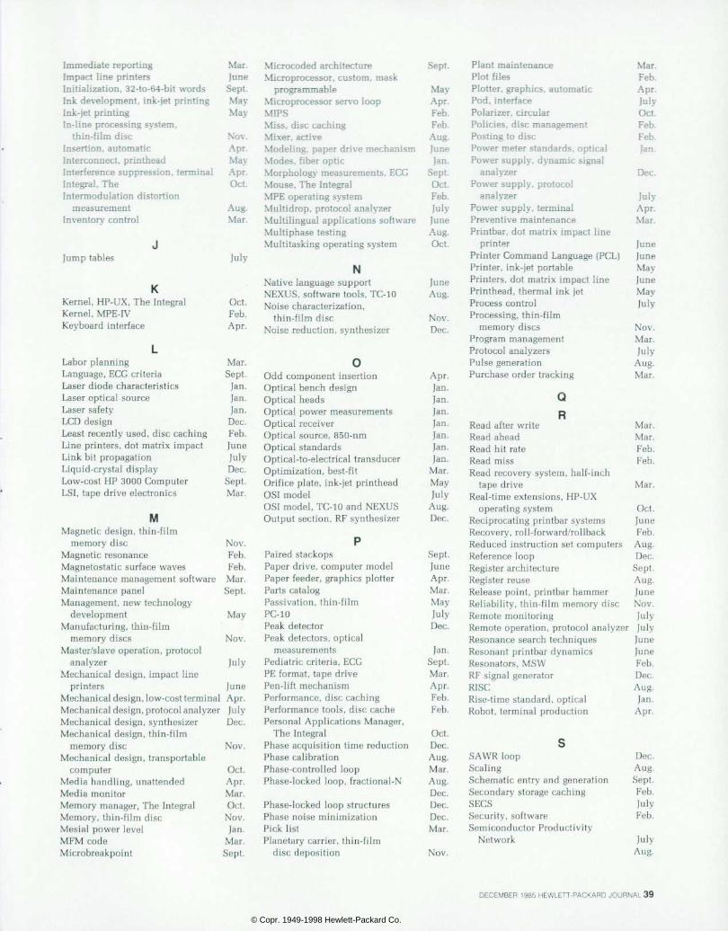
I m m e d i a t e r e p o r t i n g M a r . I m p a c t l i n e p r i n t e r s J u n e Initialization. 32-to-64-bit words Sept. Ink development, ink-jet printing May I n k - j e t p r i n t i n g M a y In-line processing system,
t h i n - f i l m d i s c N o v . I n s e r t i o n , a u t o m a t i c A p r . I n t e r c o n n e c t , p r i n t h e a d M a y Interference suppression, terminal Apr. I n t e g r a l , T h e O c t . Intermodulation distortion
m e a s u r e m e n t A u g . I n v e n t o r y c o n t r o l M a r .
J u m p t a b l e s J u l y
Kerne l , HP-UX, The In tegra l Oct . K e r n e l , M P E - I V F e b . K e y b o a r d i n t e r f a c e A p r .
L a b o r p l a n n i n g M a r . L a n g u a g e , E G G c r i t e r i a S e p t . L a s e r d i o d e c h a r a c t e r i s t i c s J a n . L a s e r o p t i c a l s o u r c e J a n . L a s e r s a f e t y J a n . L C D d e s i g n D e c . Least recently used, disc caching Feb. Line printers, dot matrix impact June L i n k b i t p r o p a g a t i o n J u l y L i q u i d - c r y s t a l d i s p l a y D e c . Low-cost HP 3000 Computer Sept . L S I , t a p e d r i v e e l e c t r o n i c s M a r .
M Magnetic design, thin-film
m e m o r y d i s c N o v . M a g n e t i c r e s o n a n c e F e b . Magne tos ta t i c sur face waves Feb . Maintenance management software Mar. M a i n t e n a n c e p a n e l S e p t . Management, new technology
d e v e l o p m e n t M a y Manufacturing, thin-film
m e m o r y d i s c s N o v . Master/slave operation, protocol
a n a l y z e r J u l y Mechanical design, impact line
p r i n t e r s J u n e Mechanical design, low-cost terminal Apr. Mechanical design, protocol analyzer July Mechanical design, synthesizer Dec. Mechanical design, thin-film
m e m o r y d i s c N o v . Mechanical design, transportable
c o m p u t e r O c t . M e d i a h a n d l i n g , u n a t t e n d e d A p r . M e d i a m o n i t o r M a r . Memory manager, The Integral Oct. M e m o r y , t h i n - f i l m d i s c N o v . M e s i a l p o w e r l e v e l J a n . M F M c o d e M a r . M i c r o b r e a k p o i n t S e p t .
M i c r o c o d e d a r c h i t e c t u r e S e p t . Microprocessor, custom, mask
p r o g r a m m a b l e M a y M i c r o p r o c e s s o r s e r v o l o o p A p r . M I P S F e b . M i s s , d i s c c a c h i n g F e b . M i x e r , a c t i v e A u g . Modeling, paper drive mechanism June M o d e s , f i b e r o p t i c J a n . Morphology measurements, EGG Sept. M o u s e , T h e I n t e g r a l O c t . M P E o p e r a t i n g s y s t e m F e b . Mul t id rop , p ro toco l ana lyzer Ju ly Multilingual applications software June M u l t i p h a s e t e s t i n g A u g . Multitasking operating system Oct.
N N a t i v e l a n g u a g e s u p p o r t J u n e NEXUS, software tools, TC-10 Aug. Noise characterization,
t h i n - f i l m d i s c N o v . Noise reduc t ion , synthes izer Dec .
O d d c o m p o n e n t i n s e r t i o n A p r . O p t i c a l b e n c h d e s i g n J a n . O p t i c a l h e a d s J a n . Op t i ca l power measurement s Jan . O p t i c a l r e c e i v e r J a n . O p t i c a l s o u r c e , 8 5 0 - n m J a n . O p t i c a l s t a n d a r d s J a n . Optical-to-electrical transducer Jan. O p t i m i z a t i o n , b e s t - f i t M a r . Orifice plate, ink-jet printhead May O S I m o d e l J u l y OSI model, TC-10 and NEXUS Aug. Output section, RF synthesizer Dec.
P a i r e d s t a c k o p s S e p t . Paper dr ive , computer model June Paper feeder , graphics plot ter Apr. P a r t s c a t a l o g M a r . P a s s i v a t i o n , t h i n - f i l m M a y P C - 1 0 J u l y P e a k d e t e c t o r D e c . Peak detectors, optical
m e a s u r e m e n t s J a n . P e d i a t r i c c r i t e r i a , E G G S e p t . P E f o r m a t , t a p e d r i v e M a r . P e n - l i f t m e c h a n i s m A p r . P e r f o r m a n c e , d i s c c a c h i n g F e b . Performance tools , disc cache Feb. Personal Applications Manager,
T h e I n t e g r a l O c t . Phase acquisition time reduction Dec. P h a s e c a l i b r a t i o n A u g . P h a s e - c o n t r o l l e d l o o p M a r . Phase-locked loop, fractional-N Aug.
Dec. Phase- locked loop s t ruc tures Dec. P h a s e n o i s e m i n i m i z a t i o n D e c . P i c k l i s t M a r . Planetary carrier, thin-film
d i s c d e p o s i t i o n N o v .
P l a n t m a i n t e n a n c e M a r . P l o t f i l e s F e b . P l o t t e r , g r a p h i c s , a u t o m a t i c A p r . P o d . i n t e r f a c e J u l y P o l a r i z e r , c i r c u l a r O c t . P o l i c i e s , d i s c m a n a g e m e n t F e b . P o s t i n g t o d i s c F e b . Power meter standards, optical Jan. Power supply, dynamic signal
a n a l y z e r D e c . Power supply, protocol
a n a l y z e r J u l y P o w e r s u p p l y , t e r m i n a l A p r . P r e v e n t i v e m a i n t e n a n c e M a r . Printbar, dot matrix impact line
p r i n t e r J u n e Printer Command Language (PCL) June P r i n t e r , i n k - j e t p o r t a b l e M a y Printers, dot matrix impact line June P r i n t h e a d , t h e r m a l i n k j e t M a y P r o c e s s c o n t r o l J u l y Processing, thin-film
m e m o r y d i s c s N o v . P r o g r a m m a n a g e m e n t M a r . P r o t o c o l a n a l y z e r s J u l y P u l s e g e n e r a t i o n A u g . P u r c h a s e o r d e r t r a c k i n g M a r .
R e a d a f t e r w r i t e M a r . R e a d a h e a d M a r . R e a d h i t r a t e F e b . R e a d m i s s F e b . Read recovery system, half-inch
t a p e d r i v e M a r . Real-time extensions, HP-UX
o p e r a t i n g s y s t e m O c t . Reciprocating printbar systems June Recovery, roll-forward/rollback Feb. Reduced instruction set computers Aug. R e f e r e n c e l o o p D e c . R e g i s t e r a r c h i t e c t u r e S e p t . R e g i s t e r r e u s e A u g . Release point, printbar hammer June Reliability, thin-film memory disc Nov. R e m o t e m o n i t o r i n g J u l y Remote operation, protocol analyzer July Resonance search techniques June R e s o n a n t p r i n t b a r d y n a m i c s J u n e R e s o n a t o r s , M S W F e b . R F s i g n a l g e n e r a t o r D e c . R I S C A u g . R i s e - t i m e s t a n d a r d , o p t i c a l J a n . R o b o t , t e r m i n a l p r o d u c t i o n A p r .
S A W R l o o p D e c . S c a l i n g A u g . Schematic entry and generation Sept. S e c o n d a r y s t o r a g e c a c h i n g F e b . S E C S J u l y S e c u r i t y , s o f t w a r e F e b . Semiconductor Productivity
N e t w o r k J u l y Aug.
DECEMBER 1985 HEWLETT-PACKARD JOURNAL 39
© Copr. 1949-1998 Hewlett-Packard Co.
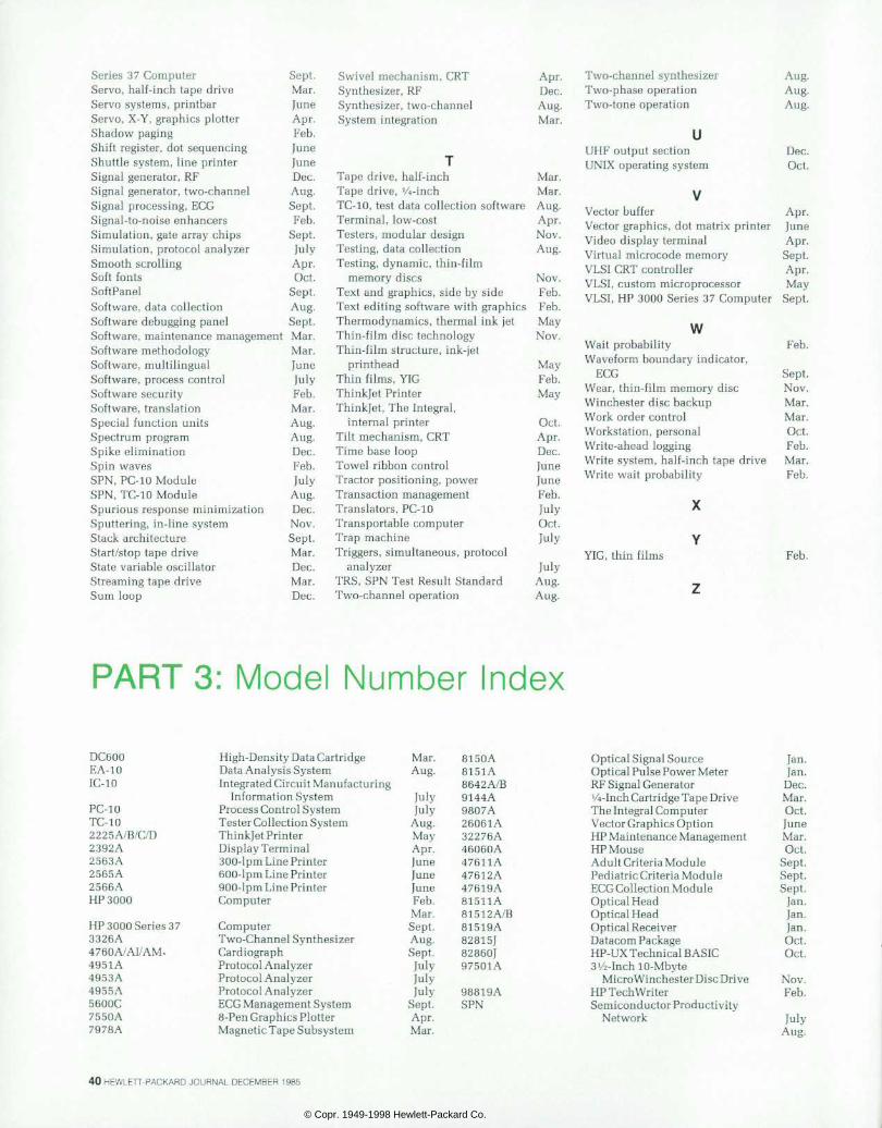
S e r i e s 3 7 C o m p u t e r S e p t . S e r v o , h a l f - i n c h t a p e d r i v e M a r . S e r v o s y s t e m s , p r i n t b a r J u n e Se rvo , X-Y, g raph ic s p lo t t e r Apr . S h a d o w p a g i n g F e b . S h i f t r e g i s t e r , d o t s e q u e n c i n g J u n e S h u t t l e s y s t e m , l i n e p r i n t e r J u n e S i g n a l g e n e r a t o r , R F D e c . Signal generator, two-channel Aug. S i g n a l p r o c e s s i n g , E G G S e p t . S i g n a l - t o - n o i s e e n h a n c e r s F e b . S imula t ion , ga te ar ray chips Sept . Simulat ion, protocol analyzer July S m o o t h s c r o l l i n g A p r . S o f t f o n t s O c t . S o f t P a n e l S e p t . S o f t w a r e , d a t a c o l l e c t i o n A u g . S o f t w a r e d e b u g g i n g p a n e l S e p t . Software, maintenance management Mar. S o f t w a r e m e t h o d o l o g y M a r . S o f t w a r e , m u l t i l i n g u a l J u n e S o f t w a r e , p r o c e s s c o n t r o l J u l y S o f t w a r e s e c u r i t y F e b . S o f t w a r e , t r a n s l a t i o n M a r . S p e c i a l f u n c t i o n u n i t s A u g . S p e c t r u m p r o g r a m A u g . S p i k e e l i m i n a t i o n D e c . S p i n w a v e s F e b . S P N , P C - 1 0 M o d u l e J u l y S P N , T C - 1 0 M o d u l e A u g . Spurious response minimization Dec. S p u t t e r i n g , i n - l i n e s y s t e m N o v . S t a c k a r c h i t e c t u r e S e p t . S t a r t / s t o p t a p e d r i v e M a r . S t a t e v a r i a b l e o s c i l l a t o r D e c . S t r e a m i n g t a p e d r i v e M a r . S u m l o o p D e c .
S w i v e l m e c h a n i s m , C R T A p r . S y n t h e s i z e r , R F D e c . S y n t h e s i z e r , t w o - c h a n n e l A u g . S y s t e m i n t e g r a t i o n M a r .
T a p e d r i v e , h a l f - i n c h M a r . T a p e d r i v e , V i - i n c h M a r . TC-10, test data collection software Aug. T e r m i n a l , l o w - c o s t A p r . T e s t e r s , m o d u l a r d e s i g n N o v . T e s t i n g , d a t a c o l l e c t i o n A u g . Testing, dynamic, thin-film
m e m o r y d i s c s N o v . Text and graphics, side by side Feb. Text editing software with graphics Feb. Thermodynamics, thermal ink jet May T h i n - f i l m d i s c t e c h n o l o g y N o v . Thin-film structure, ink-jet
p r i n t h e a d M a y T h i n f i l m s , Y I G F e b . T h i n k j e t P r i n t e r M a y Thinkjet, The Integral,
i n t e r n a l p r i n t e r O c t . T i l t m e c h a n i s m , C R T A p r . T i m e b a s e l o o p D e c . T o w e l r i b b o n c o n t r o l J u n e T r a c t o r p o s i t i o n i n g , p o w e r J u n e T r a n s a c t i o n m a n a g e m e n t F e b . T r a n s l a t o r s , P C - 1 0 J u l y T r a n s p o r t a b l e c o m p u t e r O c t . T r a p m a c h i n e J u l y Triggers, simultaneous, protocol
a n a l y z e r J u l y T R S , S P N T e s t R e s u l t S t a n d a r d A u g . T w o - c h a n n e l o p e r a t i o n A u g .
T w o - c h a n n e l s y n t h e s i z e r A u g . T w o - p h a s e o p e r a t i o n A u g . T w o - t o n e o p e r a t i o n A u g .
U U H F o u t p u t s e c t i o n D e c . U N I X o p e r a t i n g s y s t e m O c t .
V e c t o r b u f f e r A p r . Vector graphics, dot matrix printer June V i d e o d i s p l a y t e r m i n a l A p r . V i r t u a l m i c r o c o d e m e m o r y S e p t . V L S I C R T c o n t r o l l e r A p r . VLSI, custom microprocessor May VLSI, HP 3000 Series 37 Computer Sept.
W W a i t p r o b a b i l i t y F e b . Waveform boundary indicator,
E G G S e p t . Wear , th in- f i lm memory d isc Nov. W i n c h e s t e r d i s c b a c k u p M a r . W o r k o r d e r c o n t r o l M a r . W o r k s t a t i o n , p e r s o n a l O c t . W r i t e - a h e a d l o g g i n g F e b . Write system, half-inch tape drive Mar. W r i t e w a i t p r o b a b i l i t y F e b .
Y I G , t h i n f i l m s F e b .
PART 3 : Mode l Number Index
DC600 EA-10 IC-10
PC-10 TC-10 2225A/B/C/D 2392A 2563A 2565A 2566A HP 3000
HP 3000 Series 37 3326A 4760A/AI/AM- 4951A 4953A 4955A 5600C 7550A 7978A
High-Density Data Cartridge Data Analysis System Integrated Circuit Manufacturing
Information System Process Control System Tester Collection System Thinkjet Printer Display Terminal 300-lpm Line Printer 600-lpm Line Printer 900-lpm Line Printer Computer
Computer Two-Channel Synthesizer Cardiograph Protocol Analyzer Protocol Analyzer Protocol Analyzer ECG Management System 8-Pen Graphics Plotter Magnetic Tape Subsystem
Optical Signal Source Optical Pulse Power Meter RF Signal Generator Vi-Inch Cartridge Tape Drive The Integral Computer Vector Graphics Option HP Maintenance Management HP Mouse Adult Criteria Module Pediatric Criteria Module ECG Collection Module Optical Head Optical Head Optical Receiver Datacom Package HP-UX Technical BASIC avi-Inch 10-Mbyte
Micro Winchester Disc Drive HPTechWriter Semiconductor Productivity
Network
Jan. Jan.
Dec. Mar. Oct.
Mar. Oct.
Sept.
Sept. Jan. Jan. Jan. Oct. Oct.
Nov. Feb.
40 HEWLETT-PACKARD JOURNAL DECEMBER 1985
© Copr. 1949-1998 Hewlett-Packard Co.
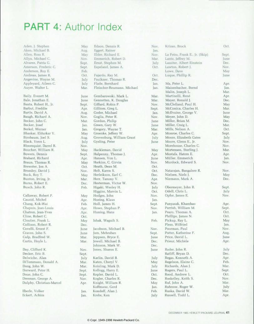
PART 4: Author Index Aden, J. Stephen Aken, Michael B. Allen. Ross R. Allyn, Michael C. Alvarez, Patria G. Amerson, Frederic C. Anderson, Roy E. Andreas, James R. Angevine, Wayne M. Appleyard, Aileen C. Auyer, Walter L.
Baily, Everett M. Bale, Jonathan E. Banta, Robert H., Jr. Barbut, Freddie Bartle, David A. Baugh, Richard A. Becker, John C. Becker, Josef Berkel, Werner Bhaskar, Eldurkar V. Birnbaum, Joel S. Black, Vonn L. Bloomquist, Darrel R. Boucher, William R. Bowers, Dennis Brabant, Richard Braun, Thomas R. Brewster, Jon A. Bromley, David J. Buck, Roy T. Bunton, Irving, Jr. Burns, Robert E. Busch, John R.
Callaway, Robert P. Cauzid, Michel Chang, Kok-Wai Chapuis, Jean-Louis Chatron, Jean-Yves Cline, Robert C. Cloutier, Frank L. Collison, Robert R. Covelli, Ernest F. Craven, John S. Culp, Bradfred W. Curtis, Hoyle L.
Day, Clifford K. Decker, Eric B. Delwiche, Alan DiTommaso, Donald A. Dong, John W. Dorward, Peter H. Doue, John C. Drennan, George A. Dulphy, Christian-Marcel
Eberle, Volker Eckert, Achim
Oct.
Sept. June Dec. Nov. May June
Apr. Jan.
Mar. Apr. Dec. May Mar. June May Dec. Mar. Oct.
Sept. July
Nov. Nov. Mar. Apr. Jan.
Nov.
Nov. May Dec.
Sept. July
Nov.
Apr. Sept. Oct. Oct . May Jan.
Nov. Aug. June Apr.
July Dec. Apr. Feb. Mar. Sept. Oct.
Nov. Mar. July
Mar. Apr.
DECEMBER 1985 HEWLETT-PACKARD JOURNAL 41
© Copr. 1949-1998 Hewlett-Packard Co.
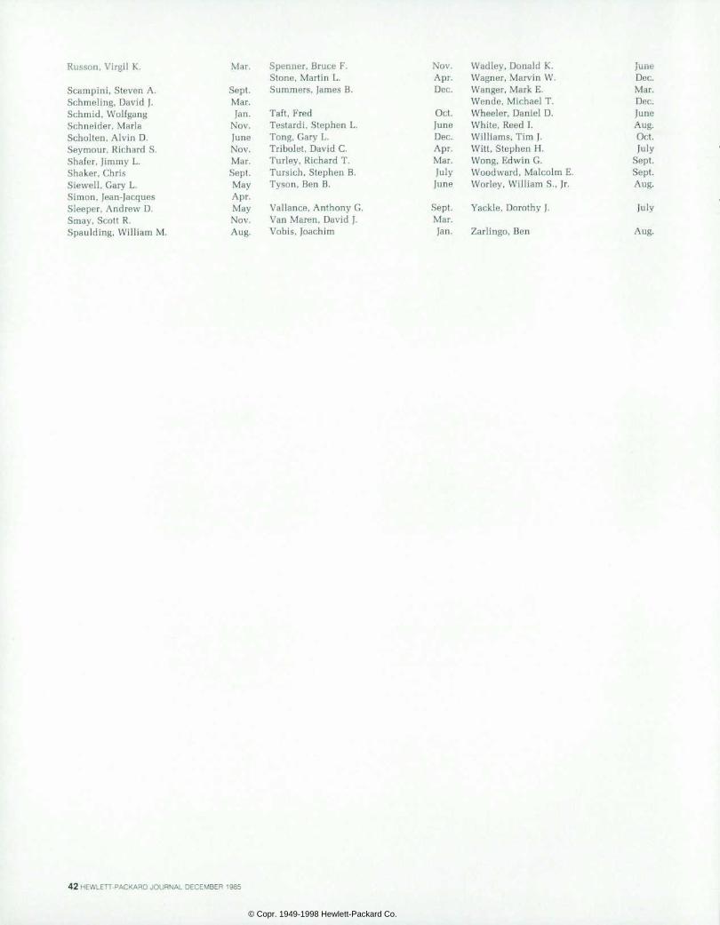
Russon, Virgil K.
Scampini, Steven A. Schmeling, David J. Schmid, Wolfgang Schneider, Maria Scholten, Alvin D. Seymour, Richard S. Shafer, Jimmy L. Shaker, Chris Siewell, Gary L. Simon, Jean-Jacques Sleeper, Andrew D. Smay, Scott R. Spaulding, William M.
Mar.
Sept. Mar. Jan.
Nov. June Nov. Mar. Sept. May Apr. May Nov. Aug.
Spenner, Bruce F. Stone, Martin L. Summers, James B.
Taft, Fred Testardi, Stephen L. Tong, Gary L. Tribolet, David C. Turley, Richard T. Tursich, Stephen B. Tyson, Ben B.
Vallance, Anthony G. Van Maren, David J. Vobis, Joachim
N o v . W a d l e y , D o n a l d K . A p r . W a g n e r , M a r v i n W . D e c . W a n g e r , M a r k E .
Wende, Michael T. Oc t . Whee le r , Dan ie l D . June White, Reed I. Dec. Williams, Tim J. Apr. Witt, Stephen H. M a r . W o n g , E d w i n G . Ju ly Woodward , Ma lco lm E . June Wor ley , Wi l l i am S . , J r .
Sep t . Yack le , Doro thy J . Mar. J a n . Z a r l i n g o , B e n
June Dec. Mar. Dec. June Aug. Oct. July
Sept. Sept. Aug.
July
Aug.
42 HEWLETT-PACKARD JOURNAL DECEMBER 1985
© Copr. 1949-1998 Hewlett-Packard Co.
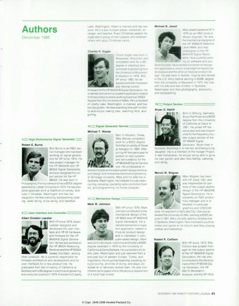
Authors December 1 985
4 H I H i g h - P e r f o r m a n c e S i g n a l G e n e r a t o r
Robert E. Burns Bob Burns i s an R&D sec tion manager who has been work ing on s igna l genera tors for HP s ince 1974. He was pro jec t manager for the HP 8642A/B and HP 8656A Signal Generators and also designed the out put sect ion for the HP 8656A. He was born in
Philadelphia, Pennsylvania and has a BSEE degree awarded by Lehigh University in 1 974. He has also done graduate work at Stanford Univers i ty . Bob l ives in Veradale, Washington and has two daughters. He l ikes camping, backpacking, boat ing, water ski ing, snow ski ing, and handbal l .
6 User In te r face and Cont ro l l e r I
Albert Einstein Lassiter With HP since 1 979, Albert Lassi ter designed and deve loped the user in te r face and HP-IB hardware and f i rmware for the HP 8642A/B S igna l Genera tors. He has also worked on
^ T J Ã ‰ 9 P l h e H P 8 9 0 2 A M e a s u r i n g - , ' , . F Receiver and the HP 8350A
^ ^ ^ ^ ^ S w e e p O s c i l l a t o r , a m o n g other products. He is current ly responsib le for f i rmware arch i tecture and development and for user inter faces for a new product l ine. He graduated from the Universi ty of Cal i fornia at Berkeley with a BS degree in electrical engineering and computer science in 1 979. A resident of Liberty
Lake, Washington. A lber t is marr ied and has two sons . He 's a jazz t rumpet p layer , composer , a r ranger , and teacher . Every Chr is tmas season he organizes a group of hom p layers who enter ta in others with jazzy Christmas carols.
R. Kogter Chuck Kogler was born in Mi lwaukee, Wisconsin and completed work for a BS degree in e lect r ica l and computer engineering from the University of Wisconsin at Madison in 1979. With HP s ince 1980 . he de signed control ler hardware and internal control
firmware for the HP 8642A/B Signal Generators. He is named coinventor on a patent application related to those products and is working toward an MSEE degree from the University of Idaho. He's a resident of L iber ty Lake, Washington, is marr ied, and has two daughters. He l ikes spending t ime with his fam i ly and enjoys making beer , watch ing f i lms, and golf ing.
1 0 Z Z S i g n a l G e n e r a t o r S e r v i c e Z Z Z Z Z Z Z Z Z Z
Michael T . Wende Born in Houston, Texas, Mike Wende comple ted work for a BSEE degree from the University of Texas at Ar l ington in 1980. Af ter joining HP the same year he worked on test systems and serviceabi l i ty for the HP 8642A/B Signal Genera- tors . His profess ional in
terests inc lude embedded system design and sup port design and he teaches electrical engineering at Gonzaga Univers i ty . Mike and his wi fe l ive in Spokane, Washington. His hobbies include motor cycl ing, camping, operat ing radio-contro l led mod e ls , and programming h is home computer .
1 4 M e c h a n i c a l D e s i g n
Mark W. Johnson With HP s ince 1979, Mark Johnson contributed to the mechanica l des ign of the HP 8663 and HP 8642A/B Signal Generators. He is named coinventor on a pa ten! appl icat ion related to
| m o d u l a r p r o d u c t d e s i g n I a n d i s i n t e r e s t e d i n c o m - I p u t e r - a i d e d d e s i g n . M a r k
was born in Burbank, California and holds a BSME degree awarded in 1979 by the Univers i ty o f California at Santa Barbara. He's a resident of Lib er ty Lake, Washington and just returned f rom a one-year tour of western Europe, Turkey, and Yugoslavia. He enjoys backpacking, kayaking, bi cyc le tour ing, a l l k inds o f sk i ing, and p lays vo l leyba l l on a nat iona l ly ranked team. He a lso con tributes some spare time to the physics department of a local h igh school .
Michael B. Jewell Mike Jewell started at HP in 1976 as an R&D Product des ign eng ineer . He was the mechanical designer of the HP 3586A/B Select ive Level Meter and was codes igner o f the HP 8642A/B Signal Gener- ators. He is currently work- i ng on so f tware and p ro
ductivity tools. He is named coinventor on two pa tent applications, one on a backlight for l iquid crys tal displays and the other on modular product de s ign. He was born in Norfo lk , Vi rg in ia and served in the U.S. Army before earn ing a BSME degree f rom the Univers i ty of Maryland in 1975. He l ives wi th h is wi fe and two chi ldren in Spokane, Washington and l ikes photography, ast ronomy, and backpack ing .
1 8 ZZ: Output Section
Bryan D . Ra t l i n Born in Bi tburg, Germany, Bryan Ratliff earned a BSEE degree f rom the Univers i ty of Cal i fornia at Davis in 1981. He jo ined HP the same year and was respon sible for the frequency dou- b ler output sect ion of the HP 8642B Signal Generator. Bryan l ives in
Spokane, Washington, is married, and has a young daughter . He is a member o f the Hunger Pro ject . A new homeowner , he en joys be ing ab le to g row h is own garden and a lso l ikes f ish ing, camping, and ski ing.
Marvin W. Wagner
 « â € ¢ P
J .
Marvin W. Wagner j M a r v W a g n e r h a s b e e n
wi th HP s ince 1981 and i w a s r e s p o n s i b l e f o r p o r
t ions of the output sect ion . des ign o f the HP 8642A/B
Signal Generators. He is ; p resen t l y an R&D p roduc - I t i v i t y manager and i s i n
terested in computer g raph ics and CAD/CAE
tools. He was born in Salt Lake City, Utah and at tended the University of Utah, earning a BSEE de gree in 1 981 . Marv, his wife, and four children live in Spokane, Washington. He is involved in youth ac t iv i t ies and sports in h is church and l ikes p lay ing softbal l and basketbal l .
Robert R. Coll ison With HP s ince 1973, Bob Co l l i son was p ro jec t man ager for the output sect ion of the HP 8642A/B Signal Generators. He has a lso contr ibuted to the develop ment of the HP 8654B Sig nal Generator , the HP
' ' J ^ C ' 8 9 0 1 A M o d u l a t i o n f f9 . *•"» Ana lyzer , and the HP 7910,
DECEMBER 1985 HEWLETT-PACKARD JOURNAL 43
© Copr. 1949-1998 Hewlett-Packard Co.
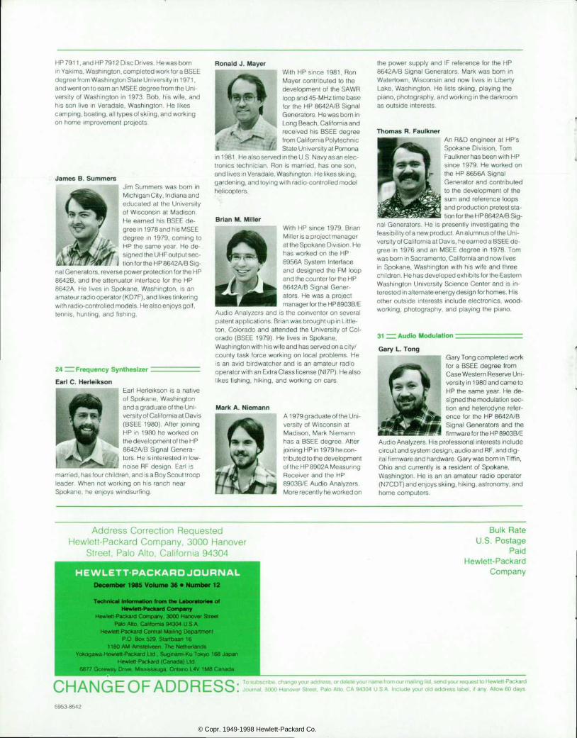
HP 791 1 , and HP 791 2 Disc Drives. He was born in Yakima, Washington, completed work for a BSEE degree from Washington State University in 1 971 , and went on to earn an MSEE degree f rom the Uni vers i ty of Washington in 1973. Bob, h is wi fe, and his son l ive in Veradale, Washington. He l ikes camping, boating, all types of skiing, and working on home improvement pro jects .
James B. Summers _ _ . , - i J i m S u m m e r s w a s b o r n i n
1 M B Ã M i c h i g a n C i t y , I n d i a n a a n d * educa ted a t t he Un i ve rs i t y
of Wisconsin at Madison. He ea rned h i s BSEE de gree in 1 978 and his MSEE degree in 1979, coming to HP the same yea r . He de signed the UHF output sec-
I t i o n f o r t h e H P 8 6 4 2 A / B S i g - nal Generators, reverse power protection for the HP 8642B, and the at tenuator inter face for the HP 8642A. He l ives in Spokane, Washington, is an amateur radio operator (KD7F), and l ikes tinkering with radio-controlled models. He also enjoys golf, tennis, hunt ing, and f ishing.
2 4 â € ” F r e q u e n c y S y n t h e s i z e r
Earl C. Herleikson Earl Herleikson is a nat ive of Spokane, Washington and a graduate of the Uni versity of California at Davis (BSEE 1980). After joining HP in 1900 he worked on the development of the HP 8642A/B S igna l Genera tors. He is interested in low- noise RF design. Earl is
married, has four children, and is a Boy Scout troop leader . When not work ing on h is ranch near Spokane, he enjoys windsurf ing.
Ronald J. Mayer ^ ^ ^ I W i t h H P s i n c e 1 9 8 1 , R o n
> * ^ ^ ^ ^ j j M a y e r c o n t r i b u t e d t o t h e t M d e v e l o p m e n t o f t h e S A W R
loop and 45-MHz time base : f o r t he HP 8642A /B S igna l ; Generators . He was born in ï Long Beach , California and
received h is BSEE degree  § ~ ^ f ^ 8 f r o m C a l i f o r n i a P o l y t e c h n i c
H i S t a t e U n i v e r s i t y a t P o m o n a in 1 981 . He also served in the U.S. Navy as an elec t ronics technic ian. Ron is marr ied, has one son, and lives in Veradale. Washington. He likes skiing, gardening, and toying with radio-control led model helicopters.
Brian M. Mil ler With HP since 1979, Br ian Miller is a project manager at the Spokane Division. He has worked on the HP 8956A System Inter face and des igned the FM loop
g . . a n d t h e c o u n t e r f o r t h e H P f t ^ * 8 6 4 2 A / B S i g n a l G e n e r -
a 'ors . He was a pro ject manager for the HP 8903B/E
Audio Analyzers and is the co inventor on severa l patent applications. Brian was brought up in Litt le ton , Co lorado and a t tended the Univers i ty o f Co l orado (BSEE 1979). He l ives in Spokane, Washington with his wife and has served on a city/ county task force work ing on loca l prob lems. He is an av id b i rdwatcher and is an amateur rad io operatorwith an Extra Class l icense (NI7P). He also l ikes f ishing, h ik ing, and working on cars.
M a r k A . N i e m a n n A 1 979 graduate of the Uni versi ty of Wisconsin at Madison, Mark Niemann has a BSEE degree. Af ter joining HP in 1 979 he con tr ibuted to the development of the HP 8902A Measuring Receiver and the HP 8903B/E Audio Analyzers. More recently he worked on
the power supply and IF re ference for the HP 8642A/B Signal Generators. Mark was born in Water town, Wisconsin and now l ives in L iber ty Lake, Washington. He l is ts ski ing, p laying the piano, photography, and working in the darkroom as outside interests.
Thomas R. Faulkner An R&D engineer at HP's Spokane Div is ion, Tom Faulkner has been with HP s ince 1979. He worked on the HP 8656A Signal Generator and contr ibuted to the development of the sum and re ference loops and product ion pretest sta t ion for the HP8642A/B Sig
nal Generators. He is present ly invest igat ing the feasibil i ty of a new product. An alumnus of the Uni versity of California at Davis, he earned a BSEE de gree in 1976 and an MSEE degree in 1978. Tom was born in Sacramento, California and now lives in Spokane, Washington wi th h is wi fe and three children. He has developed exhibits forthe Eastern Washington Univers i ty Sc ience Center and is in terested in alternate energy design for homes. His o ther outs ide in terests inc lude e lect ron ics , wood work ing, photography, and p lay ing the p iano.
3 1 = A u d i o M o d u l a t i o n ;
Gary L. Tong
.
Gary Tong completed work for a BSEE degree f rom Case Western Reserve Uni versity in 1 980 and came to HP the same yea r . He de s igned the modulat ion sec t ion and he terodyne re fe r ence for the HP 8642A/B Signal Generators and the firmware forthe HP8903B/E
Audio Analyzers. His professional interests include circuit and system design, audio and RF, and dig ital firmware and hardware. Gary was born in Tiffin, Ohio and current ly is a resident of Spokane, Washington. He is an an amateur rad io operator (N7CDT) and enjoys skiing, hiking, astronomy, and home computers.
December 1985 Volume 36 • Number 12
Technical Information from the Laborator ies of Hewlet t -Packard Company
Hewlet t -Packard Company, 3000 Hanover St ree l Pa lo A l to . Ca l i fo rn ia 94304 USA
Hewlet t -Packard Centra l Mai l ing Department P O Box 529. S tar tbaan 16
1 180 AM Amstelveen. The Nether lands Yokogawa-Hewlet t -Packard L td , Sug inami-ku Tokyo 168 Japan
Hewlet t -Packard (Canada) Ltd 6877 Goreway Dr ive, Miss issauga. Ontar io L4V 1M8
CHANG EOFADDRESS: To subscribe, change your address, or delete your name from our mail ing l ist, send your request to Hewlett-Packard Journal . 3000 Hanover St reet . Pa lo A l to . CA 94304 US. A. Inc lude your o ld address label , i f any Al low 60 days.
5953-8542
© Copr. 1949-1998 Hewlett-Packard Co.