2007 cdnlive mgh links sata slides
TRANSCRIPT
Using Allegro PCB SI GXL to Make Your Multi-GHz Serial Link Work
Right Out of the Box
Donald Telian - SI Consultant Hamid Kharrati - A2e Technologies
Session 8.11
Slide 2Donald TelianSI Consultant
AgendaAbout the ProjectModeling the SystemFrequency Domain AnalysisSignal Integrity AnalysisInterpreting Results
Slide 3Donald TelianSI Consultant
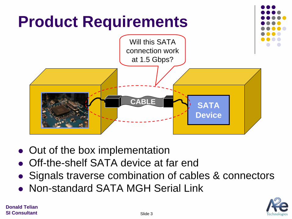
Product Requirements
Out of the box implementationOff-the-shelf SATA device at far endSignals traverse combination of cables & connectorsNon-standard SATA MGH Serial Link
CABLE SATA Device
Will this SATA connection work
at 1.5 Gbps?
Slide 4Donald TelianSI Consultant
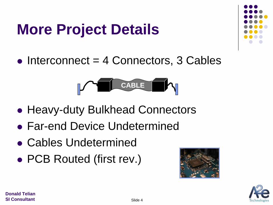
More Project Details
Interconnect = 4 Connectors, 3 Cables
Heavy-duty Bulkhead ConnectorsFar-end Device UndeterminedCables UndeterminedPCB Routed (first rev.)
CABLE
Slide 5Donald TelianSI Consultant
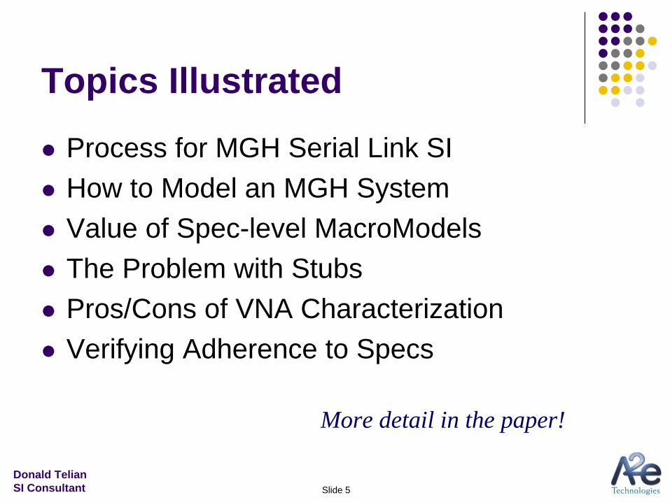
Topics Illustrated
Process for MGH Serial Link SIHow to Model an MGH SystemValue of Spec-level MacroModelsThe Problem with StubsPros/Cons of VNA CharacterizationVerifying Adherence to Specs
More detail in the paper!
Slide 6Donald TelianSI Consultant
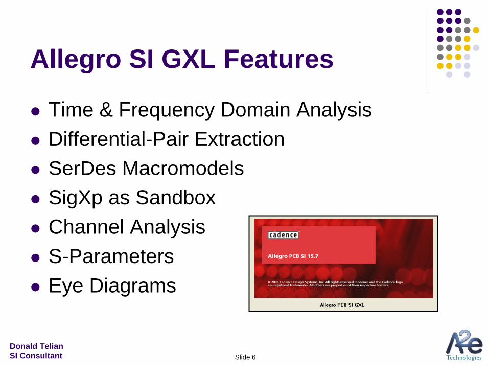
Allegro SI GXL Features
Time & Frequency Domain AnalysisDifferential-Pair ExtractionSerDes MacromodelsSigXp as SandboxChannel AnalysisS-ParametersEye Diagrams
Slide 7Donald TelianSI Consultant
AgendaAbout the ProjectModeling the SystemFrequency Domain AnalysisSignal Integrity AnalysisInterpreting Results
Slide 8Donald TelianSI Consultant
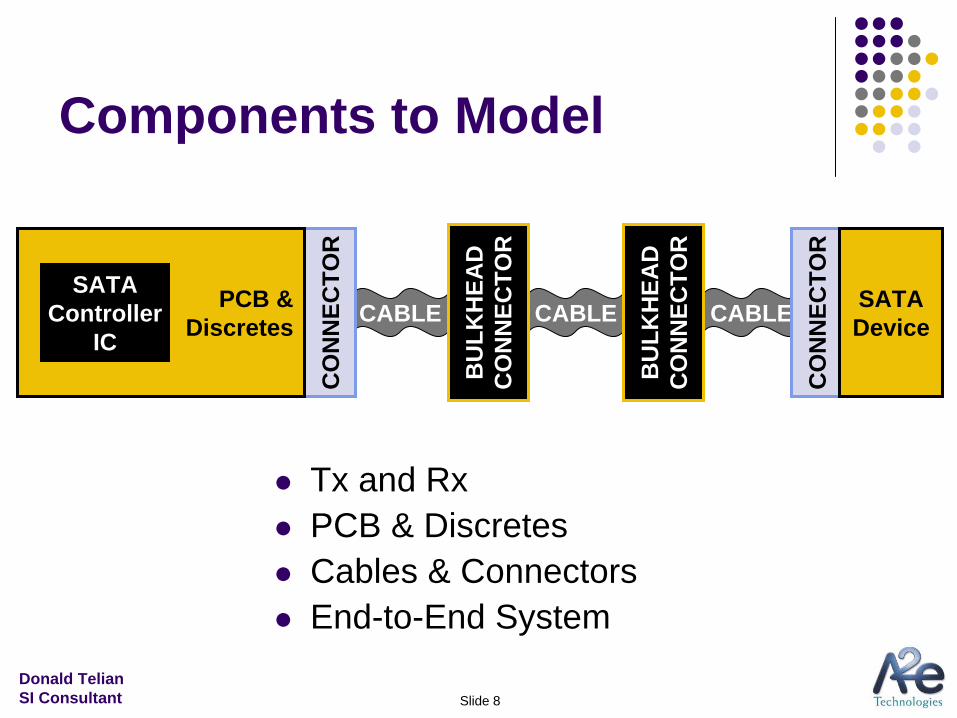
Components to Model
CABLEC
ON
NEC
TOR
CABLE
BU
LKH
EAD
C
ON
NEC
TOR
PCB & Discretes CABLE
BU
LKH
EAD
C
ON
NEC
TOR
CO
NN
ECTO
R
SATA Controller
IC
SATA Device
Tx and RxPCB & DiscretesCables & ConnectorsEnd-to-End System
Slide 9Donald TelianSI Consultant
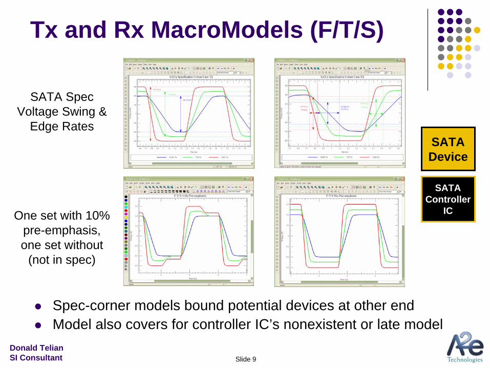
Tx and Rx MacroModels (F/T/S)
Spec-corner models bound potential devices at other endModel also covers for controller IC’s nonexistent or late model
SATA Spec Voltage Swing &
Edge Rates
One set with 10% pre-emphasis, one set without
(not in spec)
SATA Controller
IC
SATA Device
Slide 10Donald TelianSI Consultant
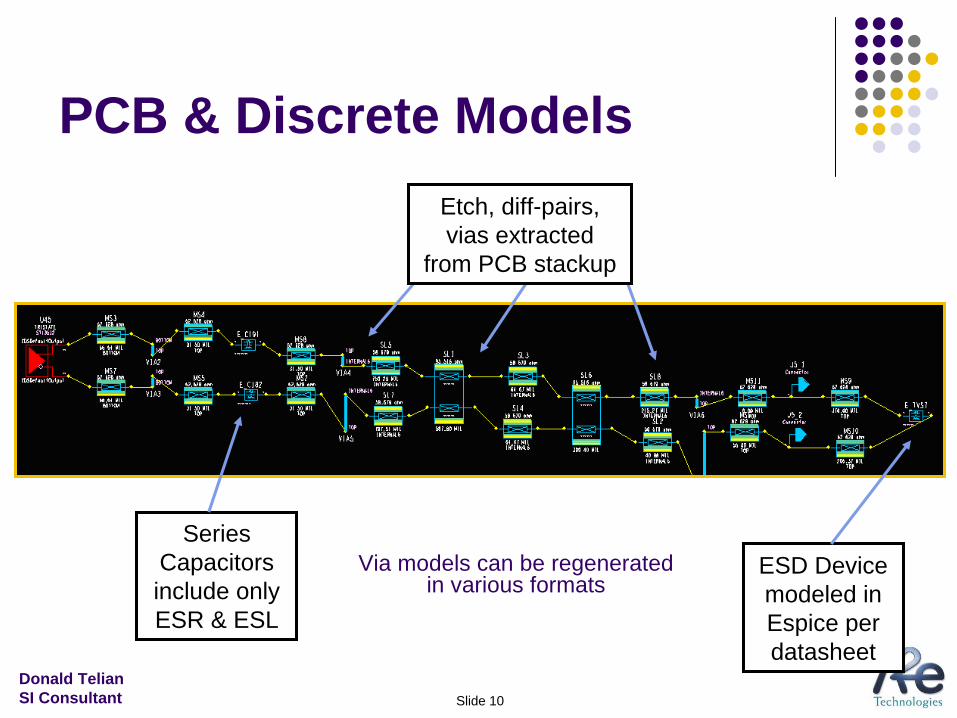
PCB & Discrete ModelsEtch, diff-pairs, vias extracted
from PCB stackup
Series Capacitors include only ESR & ESL
ESD Device modeled in Espice per datasheet
Via models can be regenerated in various formats
Slide 11Donald TelianSI Consultant
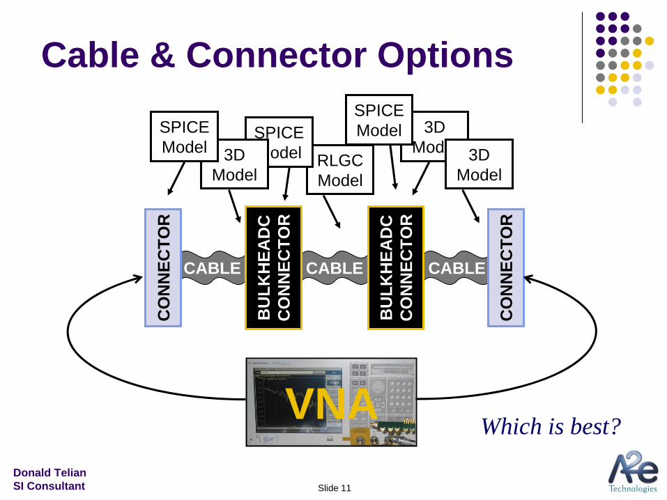
Cable & Connector Options
Which is best?
CABLE
CO
NN
ECTO
R
CABLEB
ULK
HEA
DC
C
ON
NEC
TOR
CABLE
BU
LKH
EAD
C
CO
NN
ECTO
R
CO
NN
ECTO
R
VNA
RLGC Model
3D Model
SPICE Model3D
Model
SPICE Model
3D Model
SPICE Model
Slide 12Donald TelianSI Consultant
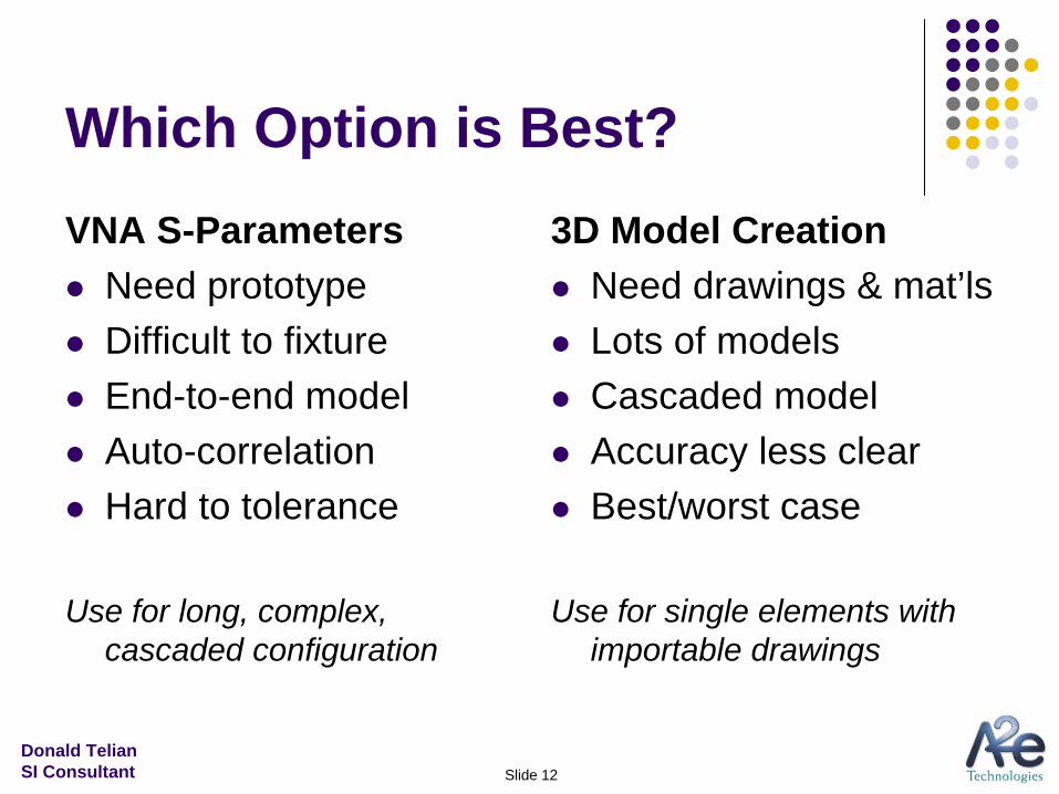
Which Option is Best?VNA S-Parameters
Need prototypeDifficult to fixtureEnd-to-end modelAuto-correlationHard to tolerance
Use for long, complex, cascaded configuration
3D Model CreationNeed drawings & mat’lsLots of modelsCascaded modelAccuracy less clearBest/worst case
Use for single elements with importable drawings
Slide 13Donald TelianSI Consultant
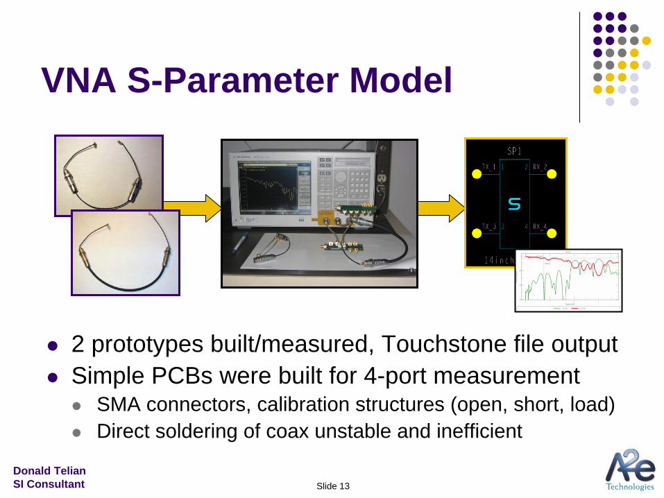
VNA S-Parameter Model
2 prototypes built/measured, Touchstone file outputSimple PCBs were built for 4-port measurement
SMA connectors, calibration structures (open, short, load)Direct soldering of coax unstable and inefficient
Slide 14Donald TelianSI Consultant
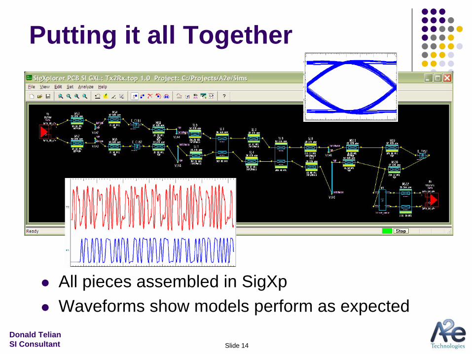
Putting it all Together
All pieces assembled in SigXpWaveforms show models perform as expected
Slide 15Donald TelianSI Consultant
AgendaAbout the ProjectModeling the SystemFrequency Domain AnalysisSignal Integrity AnalysisInterpreting Results
Slide 16Donald TelianSI Consultant
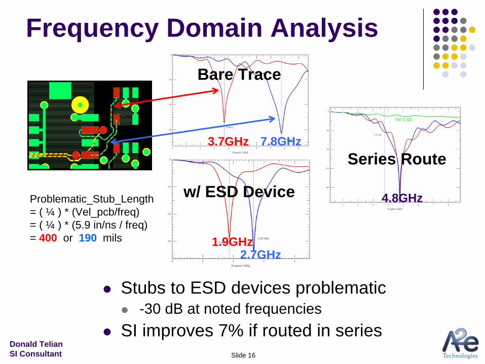
Frequency Domain Analysis
Stubs to ESD devices problematic-30 dB at noted frequencies
SI improves 7% if routed in series
Problematic_Stub_Length = ( ¼ ) * (Vel_pcb/freq) = ( ¼ ) * (5.9 in/ns / freq) = 400 or 190 mils 1.9GHz
2.7GHz
w/ ESD Device
3.7GHz 7.8GHz
Bare Trace
4.8GHz
Series Route
Slide 17Donald TelianSI Consultant
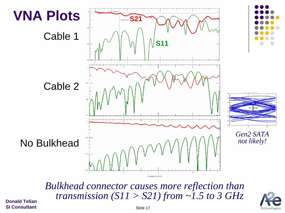
VNA PlotsCable 1
Cable 2
No Bulkhead
Bulkhead connector causes more reflection than transmission (S11 > S21) from ~1.5 to 3 GHz
S21
S11
Gen2 SATA not likely!
Slide 18Donald TelianSI Consultant
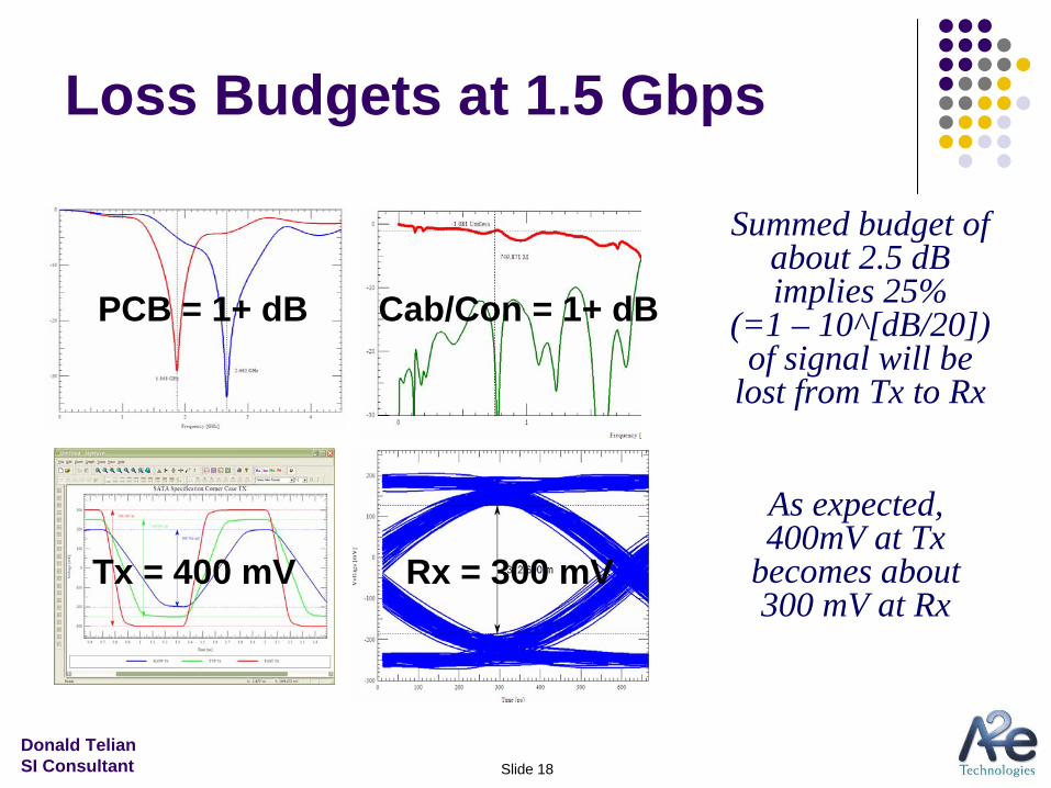
Loss Budgets at 1.5 Gbps
PCB = 1+ dB Cab/Con = 1+ dB
Summed budget of about 2.5 dB implies 25%
(=1 – 10^[dB/20]) of signal will be
lost from Tx to Rx
As expected, 400mV at Tx
becomes about 300 mV at Rx
Tx = 400 mV Rx = 300 mV
Slide 19Donald TelianSI Consultant
AgendaAbout the ProjectModeling the SystemFrequency Domain AnalysisSignal Integrity AnalysisInterpreting Results
Slide 20Donald TelianSI Consultant
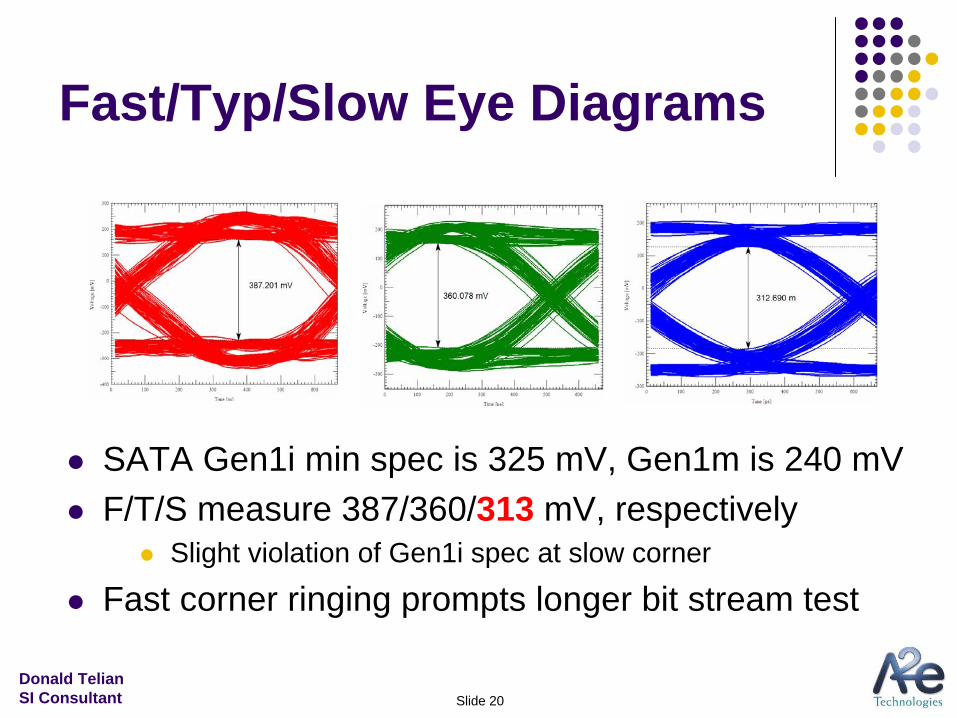
Fast/Typ/Slow Eye Diagrams
SATA Gen1i min spec is 325 mV, Gen1m is 240 mVF/T/S measure 387/360/313 mV, respectively
Slight violation of Gen1i spec at slow corner
Fast corner ringing prompts longer bit stream test
Slide 21Donald TelianSI Consultant
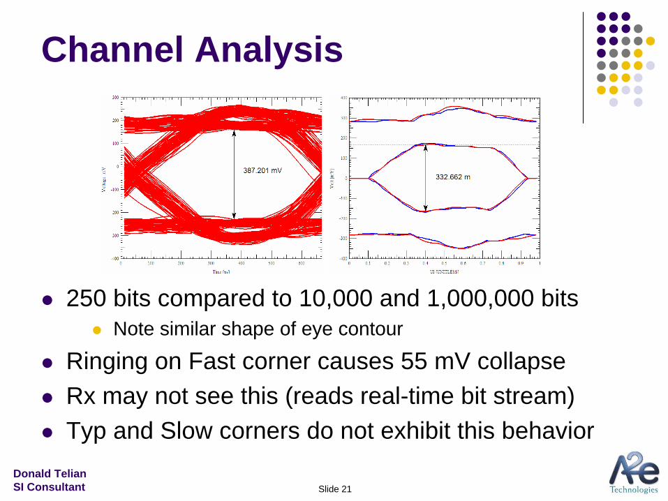
Channel Analysis
250 bits compared to 10,000 and 1,000,000 bitsNote similar shape of eye contour
Ringing on Fast corner causes 55 mV collapseRx may not see this (reads real-time bit stream) Typ and Slow corners do not exhibit this behavior
Slide 22Donald TelianSI Consultant
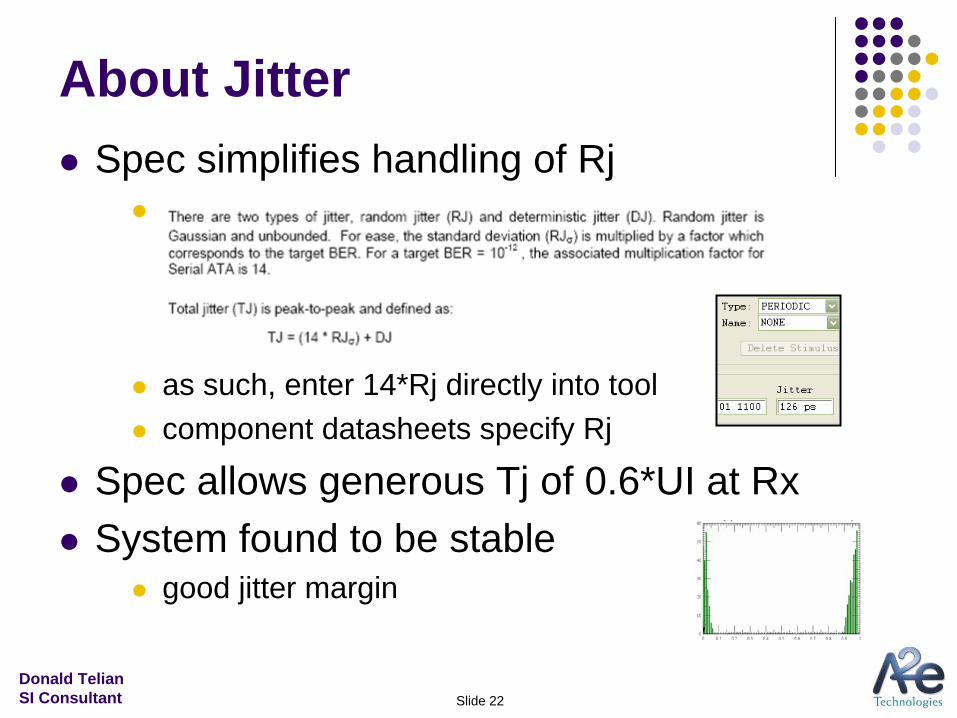
About JitterSpec simplifies handling of Rj
as such, enter 14*Rj directly into toolcomponent datasheets specify Rj
Spec allows generous Tj of 0.6*UI at RxSystem found to be stable
good jitter margin
Slide 23Donald TelianSI Consultant
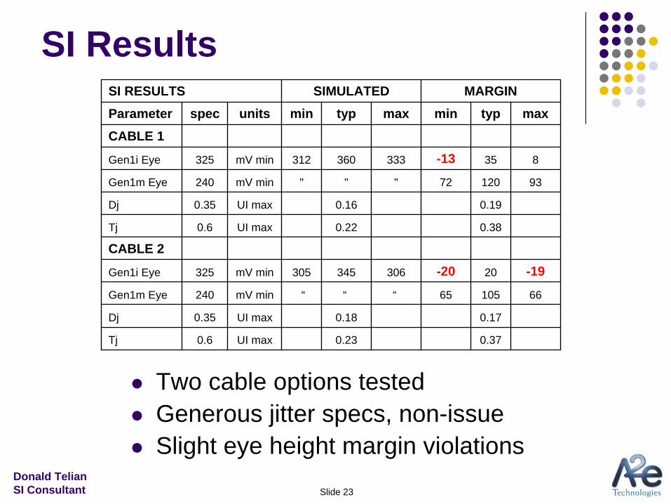
SI Results
Two cable options testedGenerous jitter specs, non-issueSlight eye height margin violations
SI RESULTS SIMULATED MARGINParameter spec units min typ max min typ maxCABLE 1
Gen1i Eye 325 mV min 312 360 333 -13 35 8
Gen1m Eye 240 mV min " " " 72 120 93
Dj 0.35 UI max 0.16 0.19
Tj 0.6 UI max 0.22 0.38
CABLE 2
Gen1i Eye 325 mV min 305 345 306 -20 20 -19
Gen1m Eye 240 mV min “ “ “ 65 105 66
Dj 0.35 UI max 0.18 0.17
Tj 0.6 UI max 0.23 0.37
Slide 24Donald TelianSI Consultant
AgendaAbout the ProjectModeling the SystemFrequency Domain AnalysisSignal Integrity AnalysisInterpreting Results
Slide 25Donald TelianSI Consultant
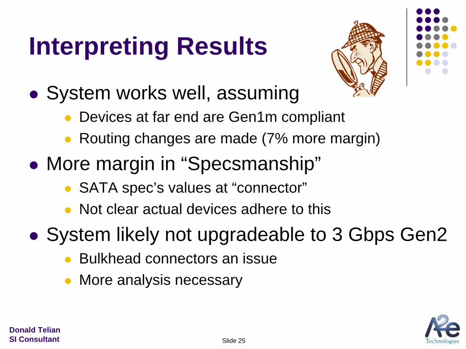
Interpreting Results
System works well, assumingDevices at far end are Gen1m compliantRouting changes are made (7% more margin)
More margin in “Specsmanship”SATA spec’s values at “connector”Not clear actual devices adhere to this
System likely not upgradeable to 3 Gbps Gen2Bulkhead connectors an issueMore analysis necessary
Slide 26Donald TelianSI Consultant
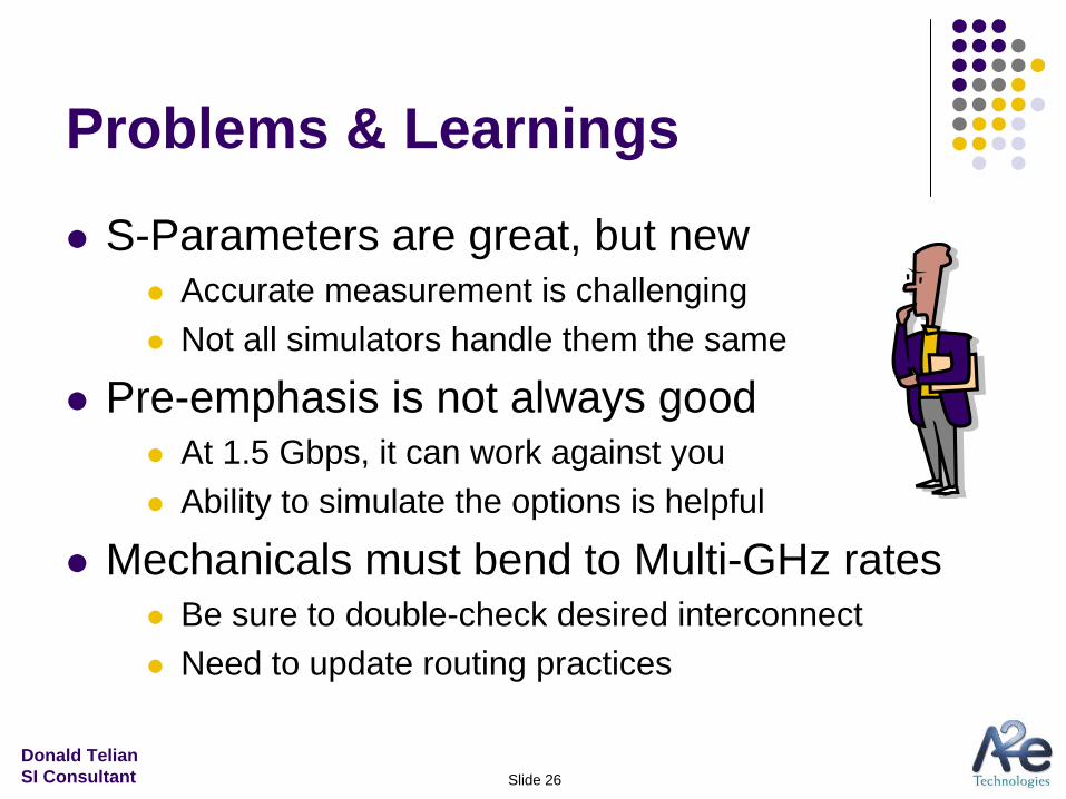
Problems & Learnings
S-Parameters are great, but newAccurate measurement is challengingNot all simulators handle them the same
Pre-emphasis is not always goodAt 1.5 Gbps, it can work against youAbility to simulate the options is helpful
Mechanicals must bend to Multi-GHz ratesBe sure to double-check desired interconnectNeed to update routing practices
Slide 27Donald TelianSI Consultant
In Conclusion
Illustrated a serial link design processHighlighted MGH modeling shortcutsDescribed how to apply Allegro PCB SIExplained new tools and techniques
…to help your design work right out of the box

THANK YOU
Slide 29Donald TelianSI Consultant