2009 inemi technology roadmapthor.inemi.org/webdownload/newsroom/presentations/2009...agenda 1 •...
TRANSCRIPT
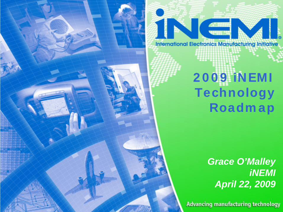
2009 iNEMI Technology
Roadmap
Grace O’MalleyiNEMI
April 22, 2009

Agenda
1
• Introduction– iNEMI and the Technology Roadmap
• 2009 Roadmap Overview– Methodology – Situational Analysis– Technology Issues and Needs
• Packaging Roadmap Highlights– Market Drivers and Trends– Single Chip Package– System in Package– Critical Research Challenges– Emerging Technologies
• Summary
1

Introduction
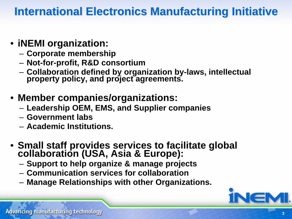
International Electronics Manufacturing Initiative
• iNEMI organization:– Corporate membership– Not-for-profit, R&D consortium– Collaboration defined by organization by-laws, intellectual
property policy, and project agreements.
• Member companies/organizations:– Leadership OEM, EMS, and Supplier companies– Government labs– Academic Institutions.
• Small staff provides services to facilitate global collaboration (USA, Asia & Europe): – Support to help organize & manage projects – Communication services for collaboration– Manage Relationships with other Organizations.
3
OEM/EMS Members
4

Supplier Members
5
Association/Consortium, Government, Consultant & University Members
6
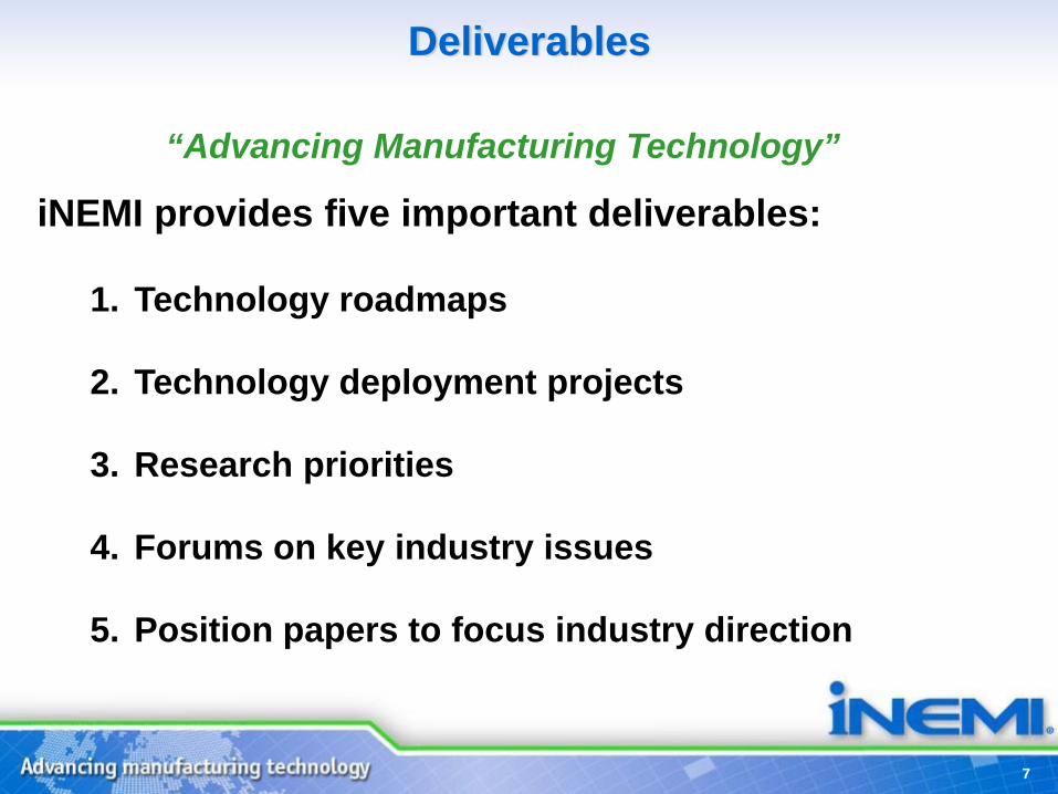
Deliverables
7
iNEMI provides five important deliverables:
1. Technology roadmaps
2. Technology deployment projects
3. Research priorities
4. Forums on key industry issues
5. Position papers to focus industry direction
“Advancing Manufacturing Technology”

iNEMI Methodology
8
Gap Analysis
iNEMIProjects
Competitive Solutions
No Work Required
Available to Market
ResearchGovernment
Academia
Disruptive Technologies
Biannual Roadmap
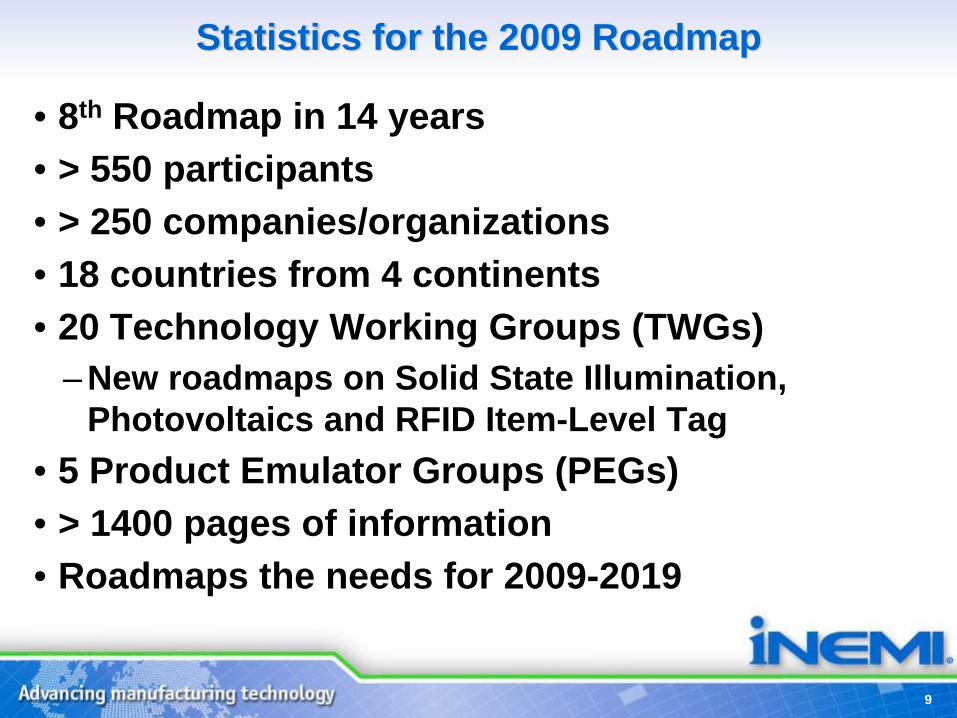
Statistics for the 2009 Roadmap
• 8th Roadmap in 14 years• > 550 participants• > 250 companies/organizations• 18 countries from 4 continents• 20 Technology Working Groups (TWGs)
– New roadmaps on Solid State Illumination, Photovoltaics and RFID Item-Level Tag
• 5 Product Emulator Groups (PEGs)• > 1400 pages of information• Roadmaps the needs for 2009-2019
9
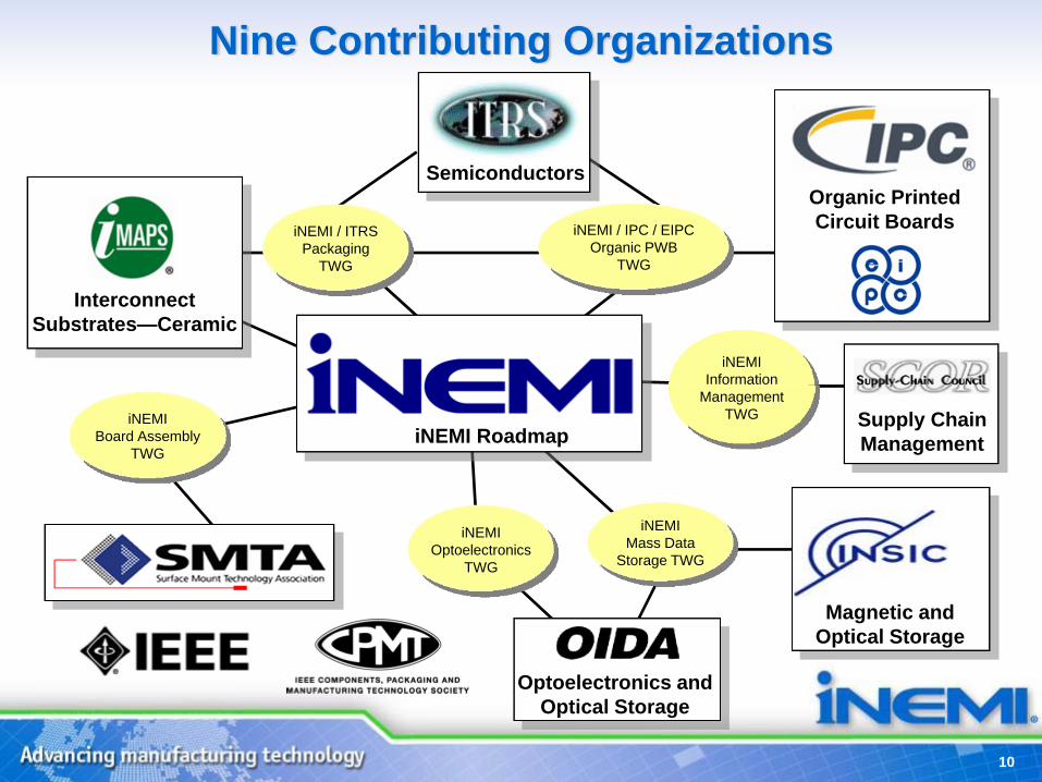
Nine Contributing Organizations
Optoelectronics and Optical Storage
Organic Printed Circuit Boards
Magnetic and Optical Storage
Supply ChainManagement
Semiconductors
iNEMIInformation
ManagementTWG
iNEMIMass Data
Storage TWG
iNEMI / IPC / EIPCOrganic PWB
TWG
iNEMI / ITRSPackaging
TWG
iNEMIBoard Assembly
TWG
Interconnect Substrates—Ceramic
iNEMI Roadmap
iNEMIOptoelectronics
TWG
10
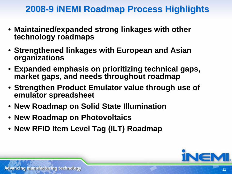
2008-9 iNEMI Roadmap Process Highlights
• Maintained/expanded strong linkages with other technology roadmaps
• Strengthened linkages with European and Asian organizations
• Expanded emphasis on prioritizing technical gaps, market gaps, and needs throughout roadmap
• Strengthen Product Emulator value through use of emulator spreadsheet
• New Roadmap on Solid State Illumination • New Roadmap on Photovoltaics• New RFID Item Level Tag (ILT) Roadmap
1111

2009 iNEMI Roadmap
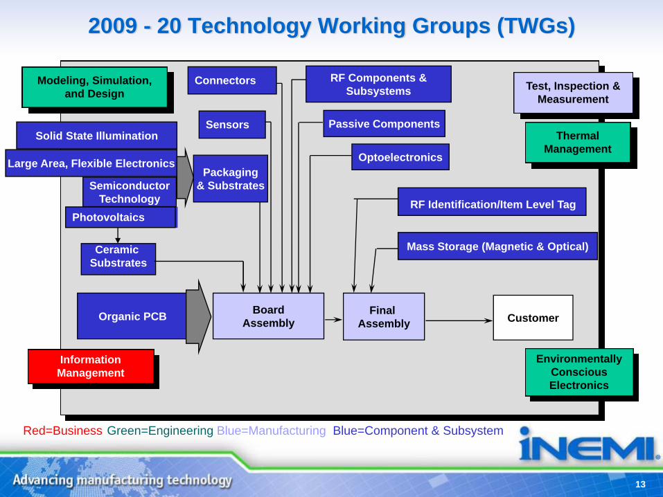
2009 - 20 Technology Working Groups (TWGs)
Organic PCB BoardAssembly Customer
RF Components & Subsystems
OptoelectronicsLarge Area, Flexible Electronics
Modeling, Simulation, and Design
Packaging& SubstratesSemiconductor
Technology
Final Assembly
Mass Storage (Magnetic & Optical)
Passive Components
Test, Inspection & Measurement
Environmentally Conscious Electronics
Ceramic Substrates
Thermal Management
Connectors
Sensors
Red=Business Green=Engineering Blue=Manufacturing Blue=Component & Subsystem
Solid State Illumination
PhotovoltaicsRF Identification/Item Level Tag
Information Management
13
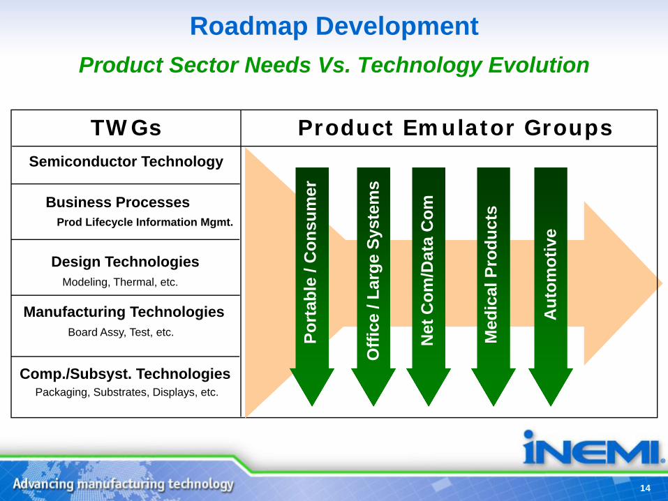
Roadmap Development
14
Product Sector Needs Vs. Technology Evolution
Product Emulator GroupsTWGs
Med
ical
Pro
duct
s
Aut
omot
ive
Net
Com
/Dat
a C
om
Semiconductor Technology
Design Technologies
Manufacturing Technologies
Comp./Subsyst. Technologies
Modeling, Thermal, etc.
Board Assy, Test, etc.
Packaging, Substrates, Displays, etc.
Business Processes Prod Lifecycle Information Mgmt.
Port
able
/ C
onsu
mer
Offi
ce /
Larg
eSy
stem
s
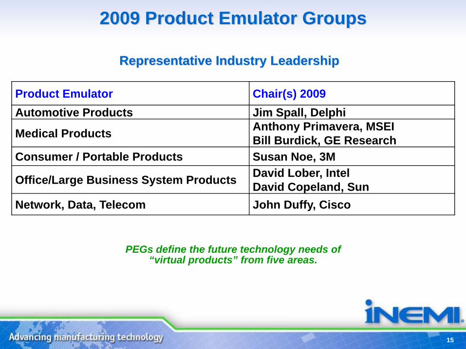
2009 Product Emulator Groups
15
Product Emulator Chair(s) 2009Automotive Products Jim Spall, Delphi
Medical Products Anthony Primavera, MSEIBill Burdick, GE Research
Consumer / Portable Products Susan Noe, 3M
Office/Large Business System Products David Lober, IntelDavid Copeland, Sun
Network, Data, Telecom John Duffy, Cisco
Representative Industry Leadership
PEGs define the future technology needs of “virtual products” from five areas.
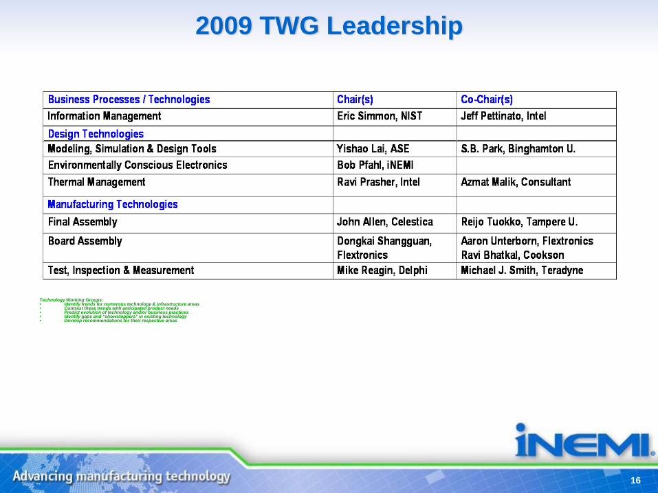
2009 TWG Leadership
16
Technology Working Groups:• Identify trends for numerous technology & infrastructure areas • Contrast these trends with anticipated product needs• Predict evolution of technology and/or business practices• Identify gaps and “showstoppers” in existing technology• Develop recommendations for their respective areas
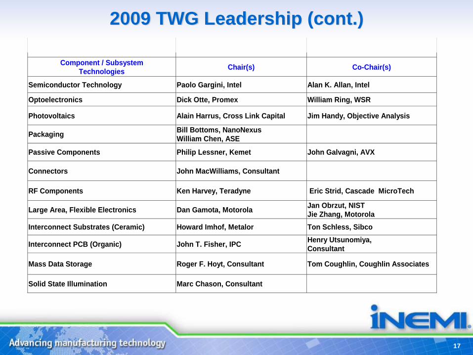
2009 TWG Leadership (cont.)
Component / Subsystem Technologies Chair(s) Co-Chair(s)
Semiconductor Technology Paolo Gargini, Intel Alan K. Allan, Intel
Optoelectronics Dick Otte, Promex William Ring, WSR
Photovoltaics Alain Harrus, Cross Link Capital Jim Handy, Objective Analysis
Packaging Bill Bottoms, NanoNexus William Chen, ASE
Passive Components Philip Lessner, Kemet John Galvagni, AVX
Connectors John MacWilliams, Consultant
RF Components Ken Harvey, Teradyne Eric Strid, Cascade MicroTech
Large Area, Flexible Electronics Dan Gamota, Motorola Jan Obrzut, NIST Jie Zhang, Motorola
Interconnect Substrates (Ceramic) Howard Imhof, Metalor Ton Schless, Sibco
Interconnect PCB (Organic) John T. Fisher, IPC Henry Utsunomiya, Consultant
Mass Data Storage Roger F. Hoyt, Consultant Tom Coughlin, Coughlin Associates
Solid State Illumination Marc Chason, Consultant
17

2009 Situational
Analysis
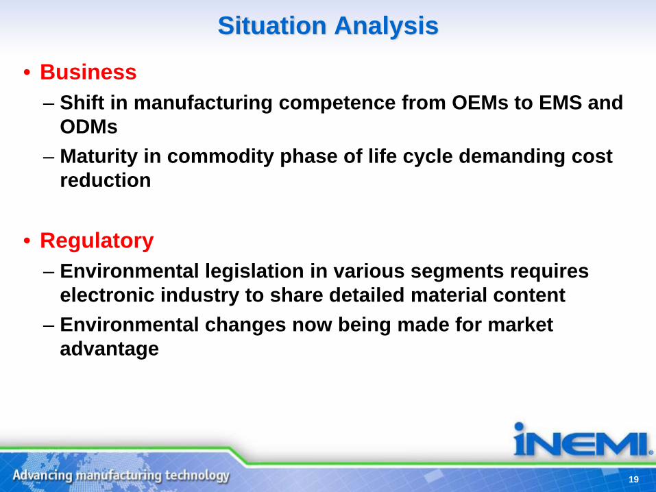
Situation Analysis
• Business– Shift in manufacturing competence from OEMs to EMS and
ODMs– Maturity in commodity phase of life cycle demanding cost
reduction
• Regulatory– Environmental legislation in various segments requires
electronic industry to share detailed material content– Environmental changes now being made for market
advantage
19
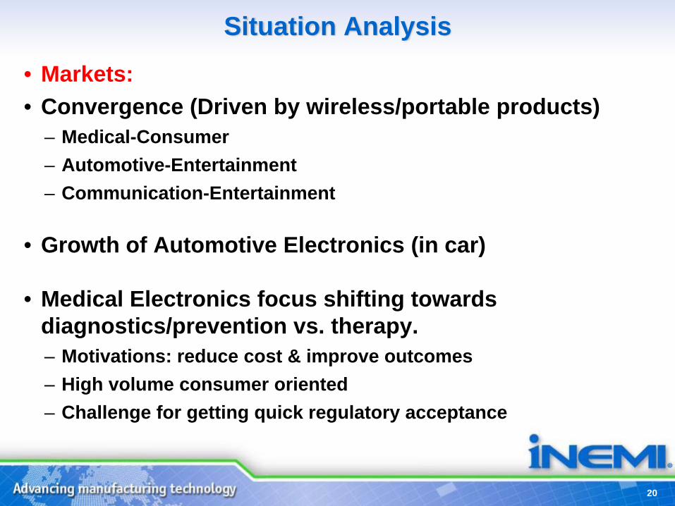
Situation Analysis
• Markets: • Convergence (Driven by wireless/portable products)
– Medical-Consumer– Automotive-Entertainment– Communication-Entertainment
• Growth of Automotive Electronics (in car)
• Medical Electronics focus shifting towards diagnostics/prevention vs. therapy.– Motivations: reduce cost & improve outcomes – High volume consumer oriented– Challenge for getting quick regulatory acceptance
20
Situation Analysis
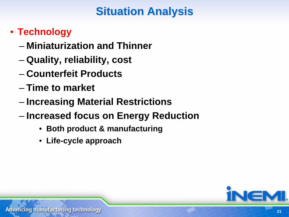
• Technology– Miniaturization and Thinner– Quality, reliability, cost– Counterfeit Products– Time to market– Increasing Material Restrictions– Increased focus on Energy Reduction
• Both product & manufacturing• Life-cycle approach
21

2009 Technology Issues and
Needs
Strategic Infrastructural Changes• The restructuring of the electronics industry over the last
decade from vertically integrated OEMs to a multi-firm supply chain has resulted in a disparity in R&D needs versus available resources
• Restructuring has created skill gaps at various nodes of supply chain
• Critical needs for research and development exist in the middle part of the supply chain (IC assembly services, passive components and EMS assembly) and yet these are the firms least capable of providing the resources
• A partial solution has been the development of vertical teams to develop critical new technology while sharing the costs
23
Key Technology Issues• Semiconductors:
– Scaling and next generation technology
• Packaging: More than Moore– New level of packaging blending Semiconductor back end and
assembly/packaging, infrastructure.– Stacked Die
• Cooling• Through hole via process and reliability• Assembly accuracy required for PoP, stacked die, etc. not consistent
with today’s Board Assembly equipment.– New capability to close the gap between chip and substrate
interconnect density:• Silicon Interposer• Organic
24
• Predictive tools for determining delaminating of new materials
• Thermal management for 3-D structures with stacked die• Co design of mechanical, thermal, bio and electrical
performance of entire chip, package and associated heat removal structures
• Design tools for emerging technologies such as embedded components and nano-materials
• Integrated design and simulation tools for high functionality in mixed mode wireless chips and modules
Design Technologies
Identified Needs
25
• Manufacturing processes to accelerate miniaturization• Assembly processes that support 3-D structures and low
temperature processing• Improved equipment accuracy for assembling stacked die,
SIPS etc.• Warpage Reduction
– Wafer– Package– PWB
• Lower testing costs, particularly for new non-digital technologies
Manufacturing Technologies
Identified Needs
26

Paradigm Shifts
27
• Wafer level packaging coming of age• Flip Chip finally is an alternative to wire bonding• Packaging materials changing over the next decade• Touch Screens becoming main stream.• MEMs oscillators replacing quartz crystals.• Emergence of photovoltaics.• Energy Efficient Lighting.• Printed electronics moving from R&D into initial applications• Flash memory instead hard drives for lower power• ODMs for Cell Phones:
– Especially for low cost models• Migration of where and how passive devices are used
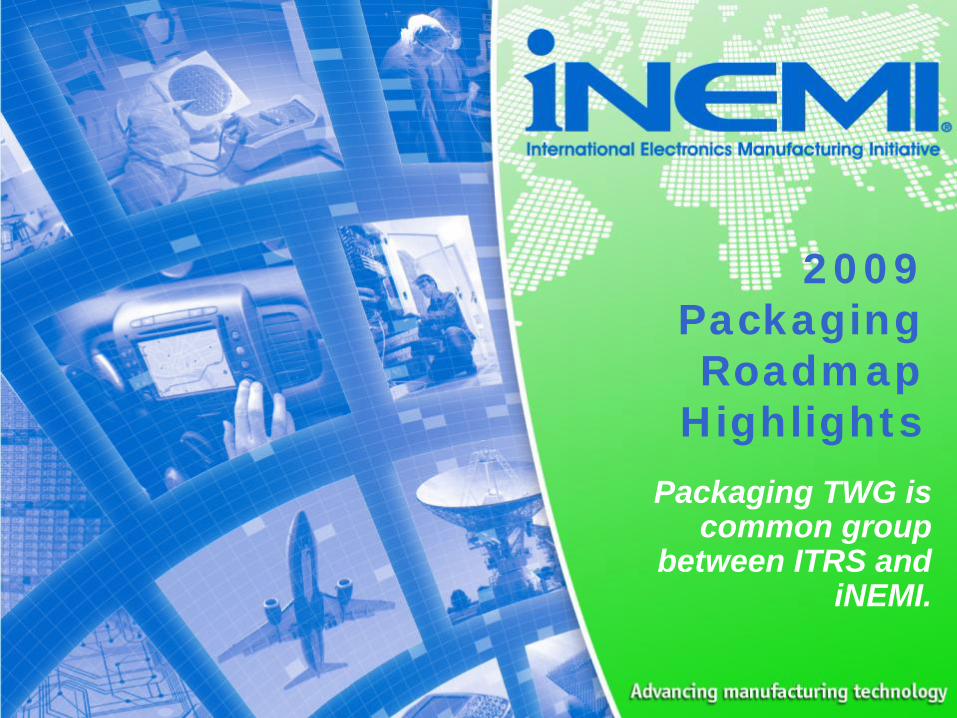
2009 PackagingRoadmap
Highlights
Packaging TWG is common group
between ITRS and iNEMI.
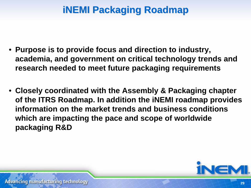
iNEMI Packaging Roadmap
• Purpose is to provide focus and direction to industry, academia, and government on critical technology trends and research needed to meet future packaging requirements
• Closely coordinated with the Assembly & Packaging chapter of the ITRS Roadmap. In addition the iNEMI roadmap provides information on the market trends and business conditions which are impacting the pace and scope of worldwide packaging R&D
29
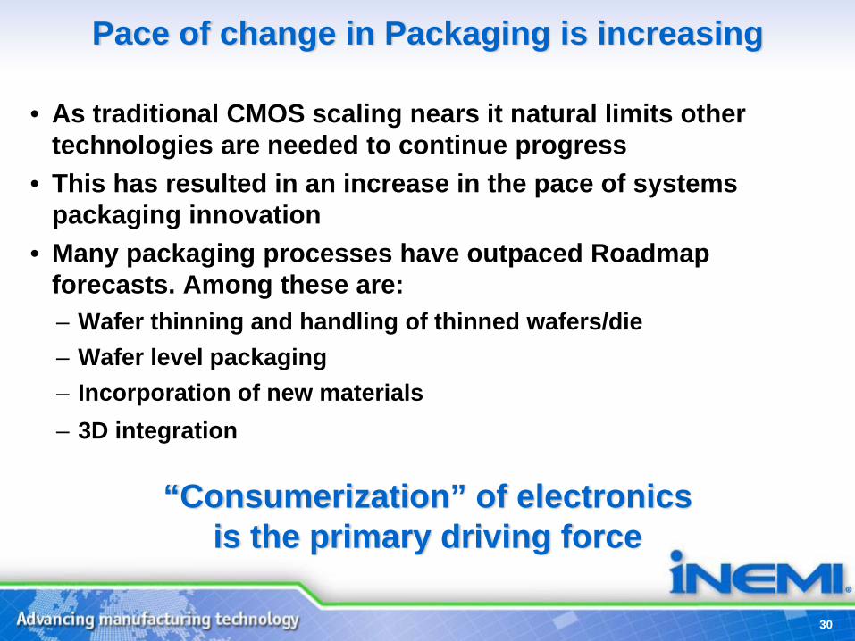
Pace of change in Packaging is increasing
• As traditional CMOS scaling nears it natural limits other technologies are needed to continue progress
• This has resulted in an increase in the pace of systems packaging innovation
• Many packaging processes have outpaced Roadmap forecasts. Among these are:– Wafer thinning and handling of thinned wafers/die– Wafer level packaging– Incorporation of new materials– 3D integration
“Consumerization” of electronics is the primary driving force
30

Moore’s Law Scaling cannot maintain the Pace of Progress and Packaging enables equivalent scaling
Interacting with people and environmentNon-digital content System-in-Package (SiP)
Beyond CMOS
Information Processing Digital content System-on-Chip (SOC)
BiochipsFluidics
SensorsActuators
HVPower
Analog/RF Passives
More than Moore : Functional Diversification
130nm
90nm
65nm
45nm
32nm
Λ...22nm
Mor
e M
oore
: Sc
alin
g
Baseline CMOS: CPU, Memory, Logic
31
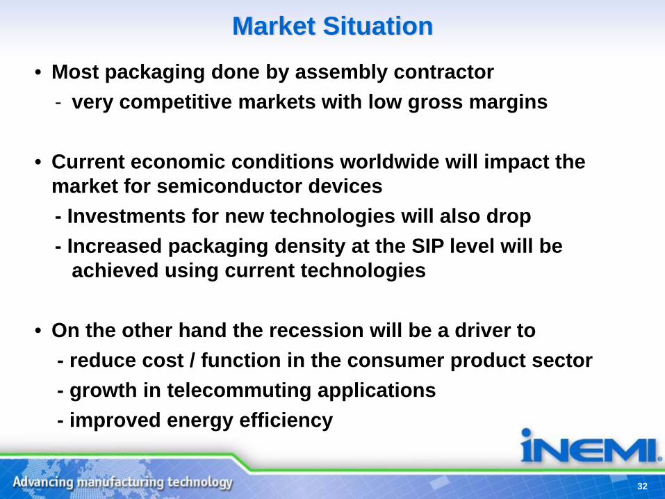
Market Situation • Most packaging done by assembly contractor
- very competitive markets with low gross margins
• Current economic conditions worldwide will impact the market for semiconductor devices- Investments for new technologies will also drop- Increased packaging density at the SIP level will be
achieved using current technologies
• On the other hand the recession will be a driver to- reduce cost / function in the consumer product sector- growth in telecommuting applications- improved energy efficiency
32
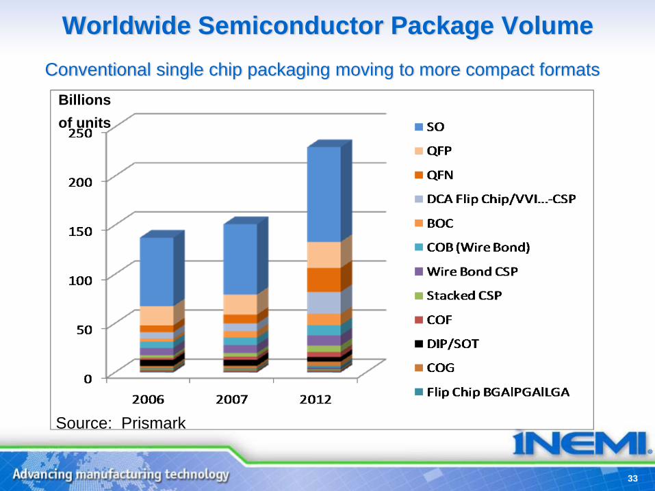
Worldwide Semiconductor Package Volume
33
Billionsof units
Conventional single chip packaging moving to more compact formats
Source: Prismark

Growth Rate by Single Chip Package Type
34
Source: Prismark
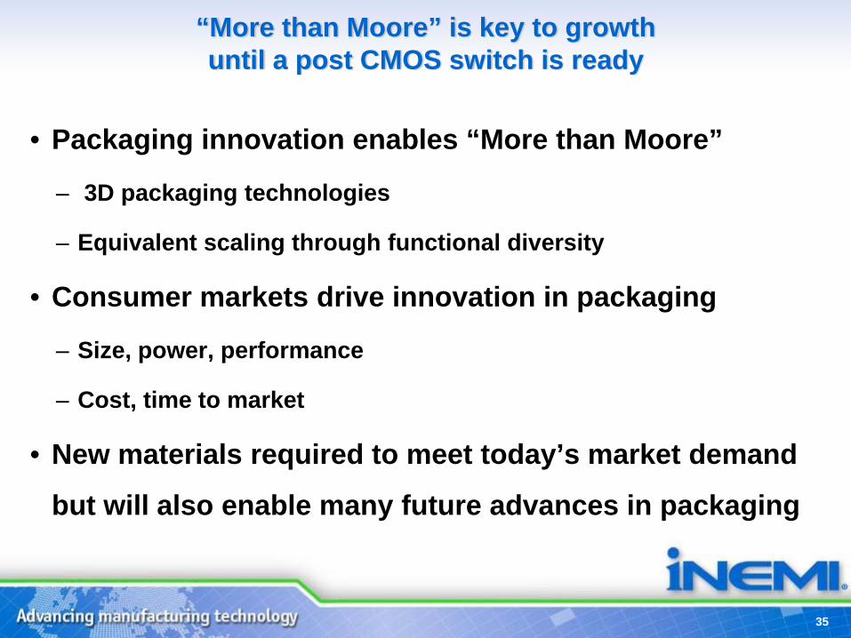
“More than Moore” is key to growth until a post CMOS switch is ready
35
• Packaging innovation enables “More than Moore”
– 3D packaging technologies
– Equivalent scaling through functional diversity
• Consumer markets drive innovation in packaging
– Size, power, performance
– Cost, time to market
• New materials required to meet today’s market demand
but will also enable many future advances in packaging
Wafer Level Packaging
36
• WLP is one of the most rapidly growing packaging technologies
– Where all IC packaging process steps are performed at wafer level
• WLP offers portable consumer products:– inherent lower cost– improved electrical performance– lower power requirements– smaller size
Wafer Level Packaging
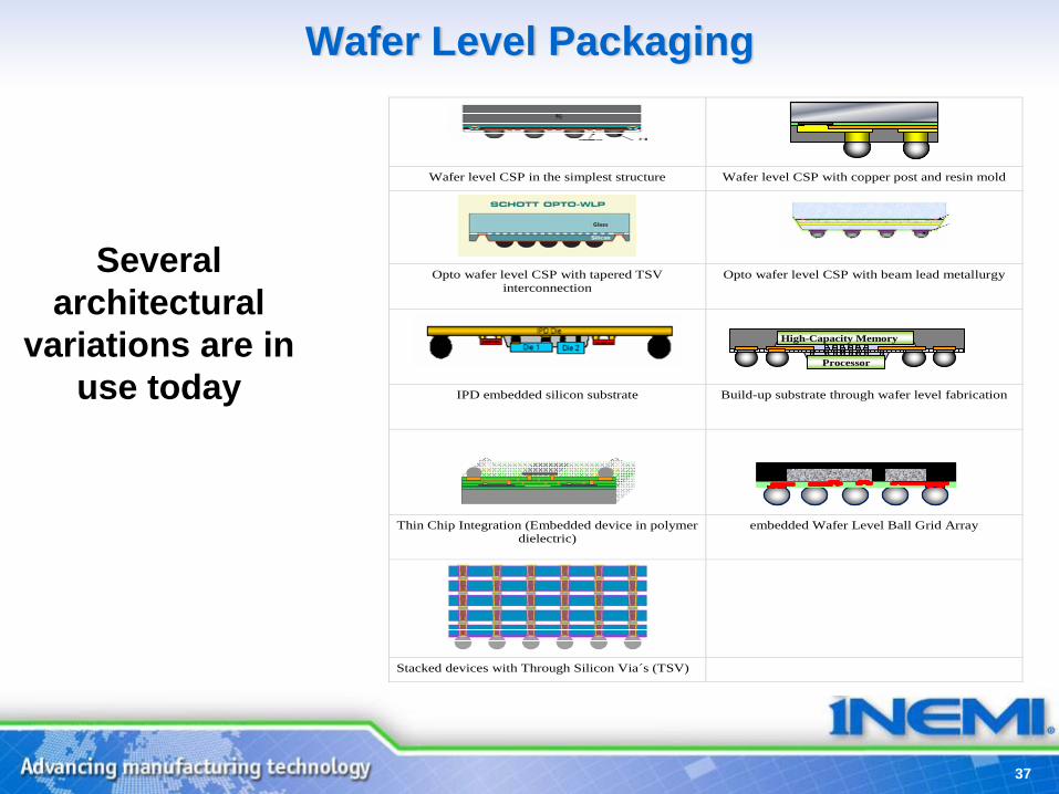
37
Wafer level CSP in the simplest structure Wafer level CSP with copper post and resin mold
Opto wafer level CSP with tapered TSV interconnection
Opto wafer level CSP with beam lead metallurgy
IPD embedded silicon substrate
Build-up substrate through wafer level fabrication
Thin Chip Integration (Embedded device in polymer dielectric)
embedded Wafer Level Ball Grid Array
Stacked devices with Through Silicon Via´s (TSV)
Processor
High-Capacity Memory
Several architectural
variations are in use today

System level Integration in the PackageThe most important trend in packaging is the incorporation of
system level integration through System in Package (SiP)
This technology enables equivalent scaling through functional diversification• Embedded active and passive components• MEMS integration • Wireless integration• Sensor integration• Analog circuit integrationWith traditional logic and memory integrated circuits
ITRS Assembly & Package System In Package White Paper
38
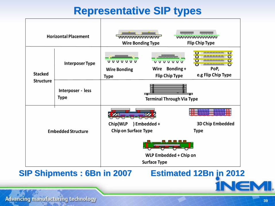
Representative SIP types
39
Horizontal Placement
StackedStructure
Interposer Type
Interposer ‐ less Type
Wire Bonding Type Flip Chip Type
Wire Bonding Type
Wire Bonding +Flip Chip Type
PoP, e.g Flip Chip Type
Terminal Through Via Type
Embedded Structure
Chip(WLP ) Embedded + Chip on Surface Type
3D Chip EmbeddedType
WLP Embedded + Chip on Surface Type
SIP Shipments : 6Bn in 2007 Estimated 12Bn in 2012
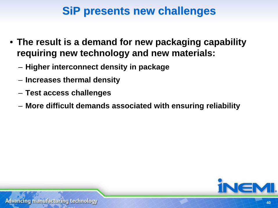
SiP presents new challenges
40
• The result is a demand for new packaging capability requiring new technology and new materials:– Higher interconnect density in package– Increases thermal density – Test access challenges– More difficult demands associated with ensuring reliability

Thermal Management Challenges
41
• High performance generates high thermal density• Heat removal requires much greater volume than the
semiconductor– Increased volume means increased wiring length causing higher
interconnect latency, higher power dissipation, lower bandwidth, and higher interconnect losses
– These consequences of increased volume generates more heat to restore the same performance
• ITRS projection for 14nm node– Power density >100W/cm2 – Junction to ambient thermal resistance <0.2degrees C/W
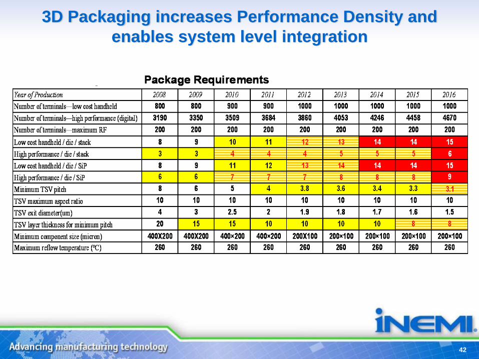
3D Packaging increases Performance Density and enables system level integration
42

Critical Research Challenges
• Major changes will be required in many areas to meet these challenges. These include:– Pb free transition presenting cost, reliability and process
compatibility problems that are not resolved (High Rel. apps.)– A new generation of DFM and DFT will be required for complex
SiP and SoC packaging– Stress induced changes in electrical properties for very thin die
will require new solutions as thinner die emerge– Reliability for through wafer vias and die layer bonding is
unproven– Warpage control for stacked die is essential for large die with fine
pitch interconnect– Interconnect for nano-scale structures– Self assembly for very small die
43
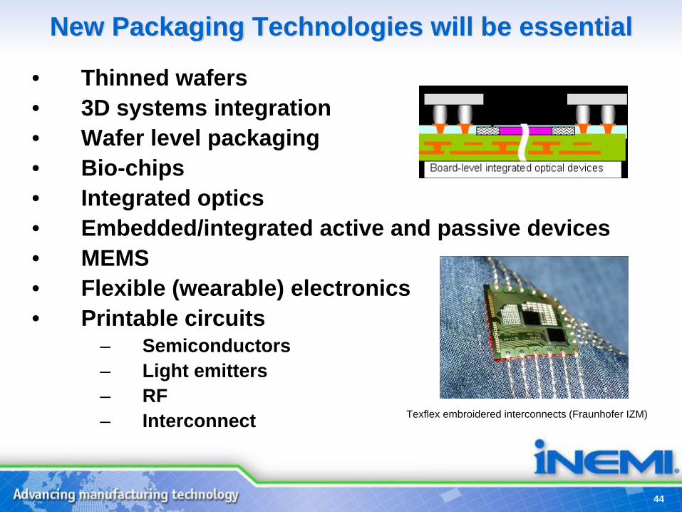
• Thinned wafers• 3D systems integration• Wafer level packaging• Bio-chips• Integrated optics• Embedded/integrated active and passive devices• MEMS• Flexible (wearable) electronics• Printable circuits
– Semiconductors– Light emitters– RF– Interconnect Texflex embroidered interconnects (Fraunhofer IZM)
New Packaging Technologies will be essential
44

Research Activities
• University Research in Packaging increasing globally
• Material companies investing in new materials beyond copper metallization and low k and High k dielectric materials for new polymer and non materials.
• Consortia/Research institutes: CALCE, EMC3D, EPACK, Fraunhofer IZM & IWMH, HDPUG, IEEC, IFC, IME, IMEC, ITRI, JIEP, KAIST, LETI, PRC, SEMATECH, SRC
Summary
Conclusions• Consumer electronics has become the major driving
force for our industry:– New technology to enable miniaturization– Relentless cost reduction– Volume manufacturing capability
• New global environmental requirements continue to multiply – faster than industry can effectively respond
• Sustainability will be a major undertaking for industry as well as society
• Electronic solutions can help to empower people to live a more sustainable lifestyle
47
Conclusions for Packaging Industry
• Packaging is Key Enabler providing higher density & smaller size:– More than Moore
– 3D configurations, Improved performance
• Many critical technology requirements yet to be met. Will need significant investment in R&D
• Cooperative development is the logical solution
48
