200w sec edition board
TRANSCRIPT
Power Conversion
Version 1.0 , September 2004
Application Note
AN-CoolMOS-09
200W SMPS Demonstration Board II
Author: Marko Scherf, Wolfgang Frank
Published by Infineon Technologies AG http://www.infineon.com
N e v e r s t o p t h i n k i n g
200W SMPS Demonstration Board II
2 of 21 AN-CoolMOS-09 V 1.0
This application note describes the 200W SMPS Demonstration Board with Infineon power products like CoolMOS, OptiMOS, TDA16888, SiC Schottky diode thinQ!, small signal N- & P-channel MOSFETs. Table of Contents 1 Features / Parameters ...........................................................................................................3 2 General Description / Main Function......................................................................................4 3 Construction / Heatsinks ........................................................................................................4 4 Description of Functional Part Groups...................................................................................5
4.1 Power Stages (“Main Board”) ..........................................................................................5 4.1.1 AC input/ EMI Filter ....................................................................................................5 4.1.2 PFC Converter ...........................................................................................................5 4.1.3 PWM Converter (Two Transistor Forward)................................................................6 4.1.4 Synchronous Rectification .........................................................................................6
4.2 Controlling Circuitry (“Control Board”) .............................................................................6 4.2.1 General Description of the Combi-IC TDA16888 ......................................................6 4.2.2 PFC Control ...............................................................................................................7 4.2.3 PWM Control..............................................................................................................7 4.2.4 Gate Drive Circuitry....................................................................................................7
5 Power Losses / Efficiency ......................................................................................................8 6 Power Loss Sources ..............................................................................................................9 7 Conducted EMI Measurements ...........................................................................................10 8 Construction of magnetic components.................................................................................11
8.1 PFC choke......................................................................................................................11 8.2 Main transformer ............................................................................................................12 8.3 Output filter choke ..........................................................................................................13
9 PCB Layout ..........................................................................................................................14 9.1 Main Board - Scaling 1:1................................................................................................14 9.2 Control Board- Scaling 1:1.............................................................................................17
10 Bill of Materials..................................................................................................................17 10.1 Main Board.....................................................................................................................17 10.2 Control Board .................................................................................................................20
Danger! This demonstration board works with mortally high voltage. Do not touch it or any other connected equipment while powered. Be aware that the board could carry high voltage for at least 5 minutes after disconnecting from mains. The unit can heat up to a high temperature. Risk of burning is given when touching. Assure yourself when working with this unit that no danger or risk can occur to the user or any other person! Do not run the main board without properly inserted control board!
200W SMPS Demonstration Board II
3 of 21 AN-CoolMOS-09 V 1.0
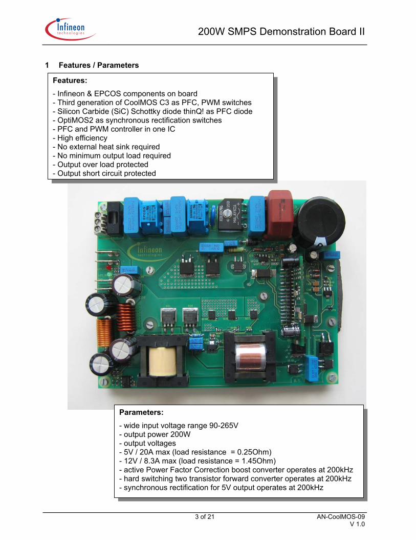
1 Features / Parameters
Parameters:
- wide input voltage range 90-265V - output power 200W - output voltages - 5V / 20A max (load resistance = 0.25Ohm) - 12V / 8.3A max (load resistance = 1.45Ohm) - active Power Factor Correction boost converter operates at 200kHz - hard switching two transistor forward converter operates at 200kHz - synchronous rectification for 5V output operates at 200kHz
Features:
- Infineon & EPCOS components on board - Third generation of CoolMOS C3 as PFC, PWM switches - Silicon Carbide (SiC) Schottky diode thinQ! as PFC diode - OptiMOS2 as synchronous rectification switches - PFC and PWM controller in one IC - High efficiency - No external heat sink required - No minimum output load required - Output over load protected - Output short circuit protected
200W SMPS Demonstration Board II
4 of 21 AN-CoolMOS-09 V 1.0
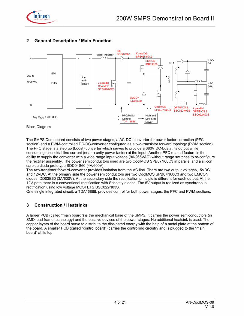
2 General Description / Main Function
Tr. 1
AC in
90-275V
EMI
Filter
Linerecti-fication
~
~ -
+Boost inductor
2 parallelCoolMOSSPB07N60C3
SICSDD04S60 CoolMOS
SPB07N60C3
EMCONIDD03E60
CoolMOSSPB07N60C3
EMCONIDD03E60
OPTIMOS 2BSC022N03S
2 parallelOPTIMOS 2BSC022N03S
+5V20A
+12V8A
High andLow SideDriver
PFC/PWMControlTDA 16888
fPFC =fPWM = 200 kHz
Block Diagram The SMPS Demoboard consists of two power stages, a AC-DC- converter for power factor correction (PFC section) and a PWM-controlled DC-DC-converter configured as a two-transistor forward topology (PWM section). The PFC stage is a step up (boost) converter which serves to provide a 380V DC-bus at its output while consuming sinusoidal line current (near a unity power factor) at the input. Another PFC related feature is the ability to supply the converter with a wide range input voltage (90-265VAC) without range switches to re-configure the rectifier assembly. The power semiconductors used are two CoolMOS SPB07N60C3 in parallel and a silicon carbide diode prototype SDD04S60 (4A/600V). The two-transistor forward-converter provides isolation from the AC line. There are two output voltages, 5VDC and 12VDC. At the primary side the power semiconductors are two CoolMOS SPB07N60C3 and two EMCON diodes IDD03E60 (3A/600V). At the secondary side the rectification principle is different for each output. At the 12V-path there is a conventional rectification with Schottky diodes. The 5V output is realized as synchronous rectification using low voltage MOSFETS BSC022N03S. One single integrated circuit, a TDA16888, provides control for both power stages, the PFC and PWM sections.
3 Construction / Heatsinks A larger PCB (called “main board”) is the mechanical base of the SMPS. It carries the power semiconductors (in SMD lead frame technology) and the passive devices of the power stages. No additional heatsink is used. The copper layers of the board serve to distribute the dissipated energy with the help of a metal plate at the bottom of the board. A smaller PCB (called “control board”) carries the controlling circuitry and is plugged to the “main board” at its top.
200W SMPS Demonstration Board II
5 of 21 AN-CoolMOS-09 V 1.0
4 Description of Functional Part Groups
4.1 Power Stages (“Main Board”)
Fuse
AC in90-255V
R1021M2
L1
C86µ47
C24µ47
C254n7
C264n7
L4
R30
~
~
+
-
C2µ47
L2500µH
rec AC+
rec AC-
R60R15
Q1B
G1B
C974n7
G1A
Q1A
VCC
R2220k
C42n2
D6
D5 VBus=380V
VBus2
C3A100n
C3150µ
G2BQ2B
GNDtop
D27
D22
Q2AG2A
S2A
R150R47
C3B
Tr. 1
C394n7
R9710R
R981R
C984n7
Q18BSP318
Q21BSC022N03S
R1001R
R1011R
Q19
BSC022N03S
Q19A
BSC022N03S
L3B
L3A
D20
C33
2n2 R454R7
R444R7
C322n2
D21 R481k8
C362200µ C36
2200µ
+12V8A
+5V20A
C154700µ
C284700µ
L5
R291R
D12TMBYV10-60
D13TMBYV10-60
C870µ47
C880µ47
C1847µ
D1113V
R284k7
Q3BSP129
D10BAV99
R801R
D76TMBYV10-60
D77TMBYV10-60
C890µ47
C900µ47
C9147µ
D7813V
R814k7
Q5BSP129
D79BAV99
GNDtop
VCCtop
VCC
XS
R391k
R205k1
R2110k
C172n2
C1668n
R195k1
IC2TL431CD
R22680R
IC3CNY17-3
D1...D4KBU8K
C101100n
R991k8
R103 47R
C992n2
C100100n
D82
1N5408
SPB07N60C3
SPB07N60C3
SPB07N60C3
SPB07N60C3
R1041k8
LED2(LC)
LED1L6
SDD04S60
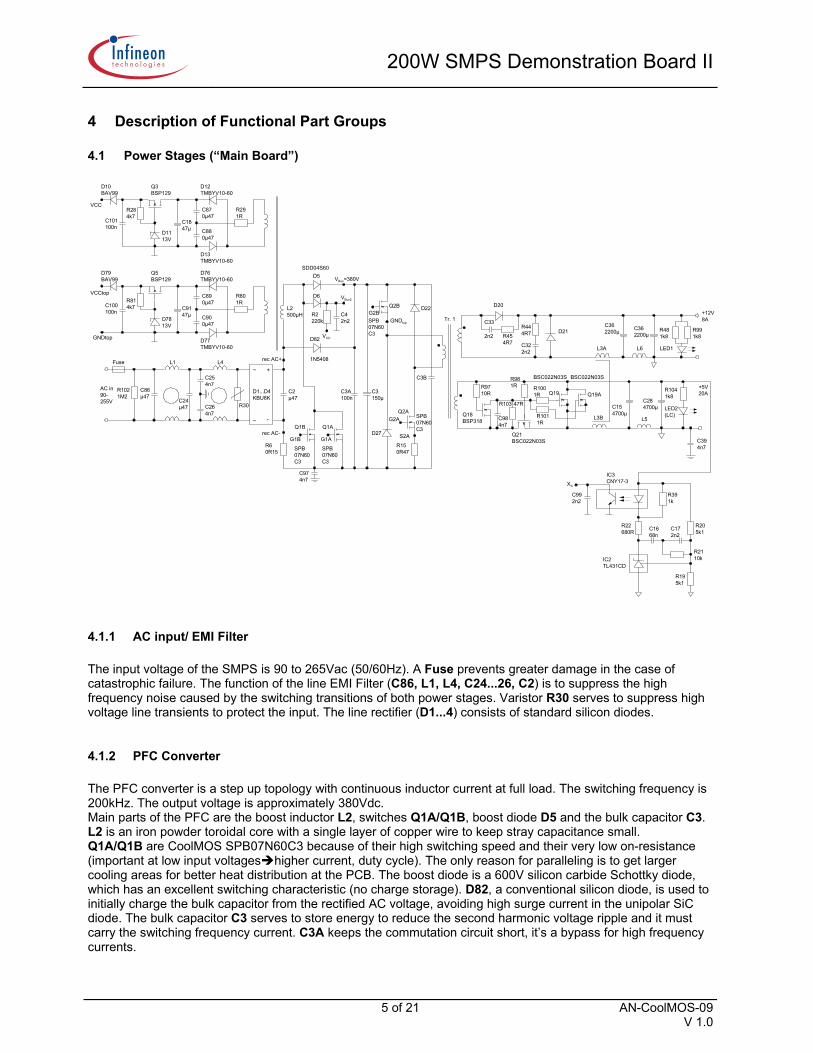
4.1.1 AC input/ EMI Filter The input voltage of the SMPS is 90 to 265Vac (50/60Hz). A Fuse prevents greater damage in the case of catastrophic failure. The function of the line EMI Filter (C86, L1, L4, C24...26, C2) is to suppress the high frequency noise caused by the switching transitions of both power stages. Varistor R30 serves to suppress high voltage line transients to protect the input. The line rectifier (D1...4) consists of standard silicon diodes.
4.1.2 PFC Converter The PFC converter is a step up topology with continuous inductor current at full load. The switching frequency is 200kHz. The output voltage is approximately 380Vdc. Main parts of the PFC are the boost inductor L2, switches Q1A/Q1B, boost diode D5 and the bulk capacitor C3. L2 is an iron powder toroidal core with a single layer of copper wire to keep stray capacitance small. Q1A/Q1B are CoolMOS SPB07N60C3 because of their high switching speed and their very low on-resistance (important at low input voltages higher current, duty cycle). The only reason for paralleling is to get larger cooling areas for better heat distribution at the PCB. The boost diode is a 600V silicon carbide Schottky diode, which has an excellent switching characteristic (no charge storage). D82, a conventional silicon diode, is used to initially charge the bulk capacitor from the rectified AC voltage, avoiding high surge current in the unipolar SiC diode. The bulk capacitor C3 serves to store energy to reduce the second harmonic voltage ripple and it must carry the switching frequency current. C3A keeps the commutation circuit short, it’s a bypass for high frequency currents.
200W SMPS Demonstration Board II
6 of 21 AN-CoolMOS-09 V 1.0
4.1.3 PWM Converter (Two Transistor Forward) The PWM converter is a two transistor forward topology. The operating frequency of 200 kHz is same as at the PFC section. Main parts at the primary side are Q2A/Q2B and D22/D27. When the forward transistors Q2A/Q2B are switched on simultaneously, energy is transferred to the output through the transformer. The transistors are chosen as CoolMOS SPB07N60C3 because of their high switching speed. D22/D27 are EMCON diodes. They serve to clamp the flyback voltages from the transformer leakage inductance, during reset of the transformer magnetization, in every turn off cycle. The transformer Tr.1 provides galvanic isolation of the output from the line and adapts the output voltages from the voltage of the bulk capacitor. The transformer consists of a ETD29/N97-core by EPCOS with tape windings. The windings are interleaved to reduce leakage inductance and winding losses. Main parts at the secondary are D20/D21, L3A, L6 and C36/C37 (12V-output) and Q19/Q21, L3B, L5 and C15, C28 (5V-output). D20/D21 are 45-volts standard Schottky diodes, which handle the current in both sequences, when the transistors are on in series rectifier mode or as freewheeling path if the transistors are off.
4.1.4 Synchronous Rectification At the 5V-path there is used a synchronous rectifier with 30V-MOSFETs BSC022N03S featuring the Super-SO8-package. It uses control waveforms generated by the secondary side of the transformer. Two MOSFETs in parallel, Q19 and Q19A handle the freewheeling current in the “low” PWM state, and one MOSFET, Q21, handles the series rectifier circuitry. The freewheeling synchronous rectifiers are turned on in the absence of the PWM pulse output, driven through the body diode of Q18 during the primary transformer reset interval. When the primary switches turn on, the gate of Q18 (previously biased negative), driven through R97 connected to the dot transformer winding, starts switching positive.
4.2 Controlling Circuitry (“Control Board”)
1
2
3
4
5
6
7
8
9
10
20
19
18
17
16
15
14
13
12
11
C9A2n2
R4B470k
R4A470k
recAC+
Vref
C12µ47
R810k
R51k8
C7220p
C82n2
R71k8R3
10k
R2633k
C1047p
C11µ47
C11A220µ
C21100p R32
1k
C14µ47
open
R2333k
R351k
R2422k
C224n7C13
47p
R1451k
R16 390kR13D820k
R13C1M
R13B1M
R13A1M
C6 100n
C41 220pC5 47n
R11 51k
R2510k
R27 51k
R12D
820k
R12C R12B R12A
1M 1M 1M
R1D820k
R1C1M
R1B1M
R1A1M
S2A
XS
Vref
VBus = 380V
VBus2
PWMout
VCC
PFCout
Vref
recAC-
IC1 TD
A 16888
Vref
PWMout
PFCout
VCC
GND
PFCCL
GNDS
PFCCS
PFCCC
ac Aux vs
PFCVS
PFCVC
PFCFB
Rosc
PWMRMP
PWMIN
PWMSS
SYNC
PWMCS
D80BAV99
C93100p
R921k
R911k
D81BAV99
VCCtop
R9310R
C94100n
C9547µ
C96µ47
VDDtop
IC9HEF40106BT
1421
3
5
9
11
9
13
4
6
8
10
12
7
Q14BC817
Q15BC807
R944R7
Q16BSP613P
R9568R
R9610R
Q17BSP320S
G2B
GNDtop
1421
3
5
4
6
Q6BC817
Q7BC807
R834R7
Q8BSP613P
R8668R
R8710R
Q9BSP320S
G1BG1A
R8468R
R8510R
89
11
13
10
12
Q10BC817
Q11BC807
R884R7
Q12BSP613P
R8968R
R9010R
Q13BSP320S
G2A
7
R8210R
C92µ47
PFCout
PWMout
VDD
IC7HEF40106BT
VCC
IC8SFH6711
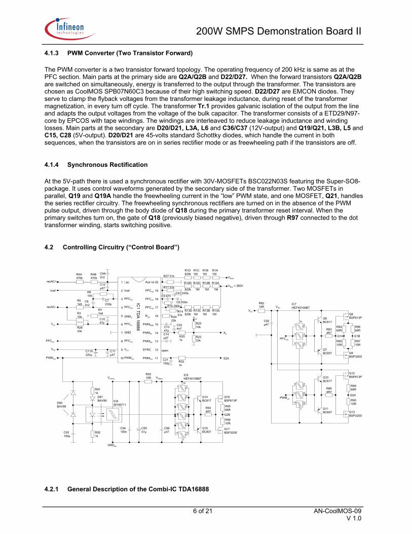
4.2.1 General Description of the Combi-IC TDA16888
200W SMPS Demonstration Board II
7 of 21 AN-CoolMOS-09 V 1.0
The TDA 16888 comprises the complete control for power factor controlled switched mode power supplies. With its PFC and PWM section being internally synchronized, it is suitable for two stage off-line converters with worldwide input voltage range. It is designed to reduce system costs by less external parts count. Special PFC features include: • Dual loop control (average current and voltage sensing) • Additional operation mode as auxiliary power supply • Fast, soft switching totem pole gate drive (1A) • Leading edge pulse width modulation • Peak current limitation • Overvoltage protection Special PWM features include: • Improved current mode control • Fast, soft switching totem pole gate drive (1A) • Soft-start management • Trailing edge pulse width modulation • 50% maximum duty cycle to prevent transformer saturation • Individually adjustable Power Management
4.2.2 PFC Control The TDA 16888 provides active power factor control in average current control mode. The “heart” of the PFC section is an analog multiplier. It creates the current programming signal for the current amplifier OP2 by multiplying the rectified line voltage with the output of the voltage amplifier so that the current programming signal has the shape of the input voltage and an average amplitude which controls the output voltage. At the Demoboard the external circuitry of the voltage amplifier (voltage sensing, compensating) consists of R13, R14, R16, C5, and C6. The resistor R4 serves to monitor the actual rectified line voltage. R5, R7, R8, C7, and C8 are the components belonging to the current amplifier, the inductor current is monitored as a voltage drop at R6 (located at “main board”). R3, R26 determine the PFC current limit (approx. 6,5A). R11, R12 fix the overvoltage thresholds.
4.2.3 PWM Control The TDA 16888 provides an improved current mode control containing effective slope compensation as well as enhanced spike suppression. The converter primary side switch current is monitored as voltage drop at R15 (located at “main board”). The amplified and “cleaned” current signal sensed at PWMCS (11), measurable at PWMRMP (15), together with the output voltage control loop feedback signal at PWMIN (14), are both inputs of the PWM comparator C8. Together they determine the actual duty cycle. C14 provides soft start of the PWM section. The components of the output voltage control loop are located at the secondary side of the converter (on the “main board”). The feedback signal is transferred across the isolation barrier via a low cost optocoupler, IC3.
4.2.4 Auxiliary Power Supply /Gate Drive Circuitry The supply voltage of the control circuitry is generated by an additional winding of the PFC choke L2. This cost- efficient technique is featured by the TDA 16888 because of a special control loop, which ensures a continuous generation of auxiliary power even at no load condition and sudden load drops. Because of the very high operating frequency the PFC section power transistors (Q1A, Q1B) and the low side power transistor (Q2A) of the PWM stage are driven by discrete high speed, high current driver stages using small signal bipolar transistors and MOSFETs. That’s why the original gate drive signals at PFCOUT/ PWMOUT are schmitt-trigerred and used as inputs of the discrete drivers. The gate drive signal of the high side power transistor (Q2B) is transferred via a high-speed optocoupler, IC8 (SFH 6711), and amplified as described before. The floating supply voltage for the high side driver circuitry is generated by another separate winding of L2.
200W SMPS Demonstration Board II
8 of 21 AN-CoolMOS-09 V 1.0
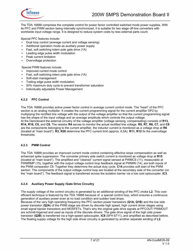
5 Power Losses / Efficiency Measured power losses at nearly full load and different input voltages:
Vinac/V Pin/W Pout/W V12v/V I12v/A V5v/V I5v/A η/% 90 225 185,0 10,25 7,2 5,03 22,1 82,2
110 222 185,0 10,25 7,2 5,03 22,1 83,3 150 218 185,0 10,25 7,2 5,03 22,1 84,9 200 217 185,0 10,25 7,2 5,03 22,1 85,3 230 215 185,0 10,25 7,2 5,03 22,1 86,0 275 215 185,0 10,25 7,2 5,03 22,1 86,0
The best efficiency appears at high input voltage, the worst at the lowest. The reason is the variation of the line current. Higher input currents result in increased conduction losses at the input rectifier, EMI Filter, PFC choke and PFC current sense resistor. The RMS value of the PFC transistor current is much higher at low line conditions, when the switches have to carry higher peak currents. Furthermore, the transistors switch at twice the effective duty cycle in order to provide a higher step up rate for the PFC stage. The higher current values also cause increased switching losses of the PFC stage. The behavior of the PWM stage doesn’t depend on the input voltage, due to the pre-regulated bulk bus from the output of the PFC stage.
82,283,3
85,3 86 8684,9
50
55
60
65
70
75
80
85
90
50 100 150 200 250 300
Vin AC [V]
Effic
ienc
y [%
]
200W SMPS Demonstration Board II
9 of 21 AN-CoolMOS-09 V 1.0
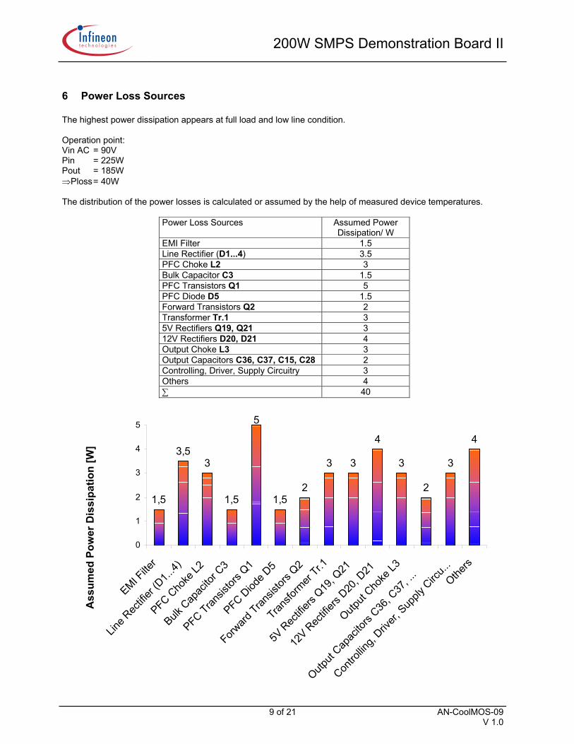
6 Power Loss Sources The highest power dissipation appears at full load and low line condition. Operation point: Vin AC = 90V Pin = 225W Pout = 185W ⇒Ploss = 40W The distribution of the power losses is calculated or assumed by the help of measured device temperatures.
Power Loss Sources Assumed Power Dissipation/ W
EMI Filter 1.5 Line Rectifier (D1...4) 3.5 PFC Choke L2 3 Bulk Capacitor C3 1.5 PFC Transistors Q1 5 PFC Diode D5 1.5 Forward Transistors Q2 2 Transformer Tr.1 3 5V Rectifiers Q19, Q21 3 12V Rectifiers D20, D21 4 Output Choke L3 3 Output Capacitors C36, C37, C15, C28 2 Controlling, Driver, Supply Circuitry 3 Others 4 ∑ 40
1,5
3,53
1,5
5
1,52
3 3
4
3
2
3
4
0
1
2
3
4
5
EMI Filte
r
Line R
ectifi
er (D
1...4)
PFC Cho
ke L2
Bulk C
apac
itor C
3
PFC Transis
tors Q
1
PFC Diod
e D5
Forward
Transis
tors Q
2
Transfo
rmer
Tr.1
5V R
ectifi
ers Q
19, Q
21
12V R
ectifi
ers D
20, D
21
Output
Choke
L3
Output
Capac
itors
C36, C
37, ..
.
Contro
lling,
Driver,
Sup
ply C
ircu..
.
Others
Ass
umed
Pow
er D
issi
patio
n [W
]
200W SMPS Demonstration Board II
10 of 21 AN-CoolMOS-09 V 1.0
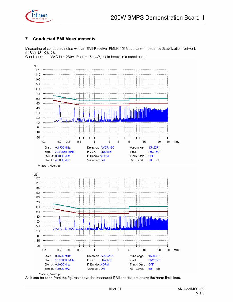
7 Conducted EMI Measurements Measuring of conducted noise with an EMI-Receiver FMLK 1518 at a Line-Impedance Stabilization Network (LISN) NSLK 8128. Conditions: VAC in = 230V, Pout = 181,4W, main board in a metal case.
Phase 1, Average
Phase 2, Average
As it can be seen from the figures above the measured EMI spectra are below the norm limit lines.
200W SMPS Demonstration Board II
11 of 21 AN-CoolMOS-09 V 1.0
8 Construction of magnetic components
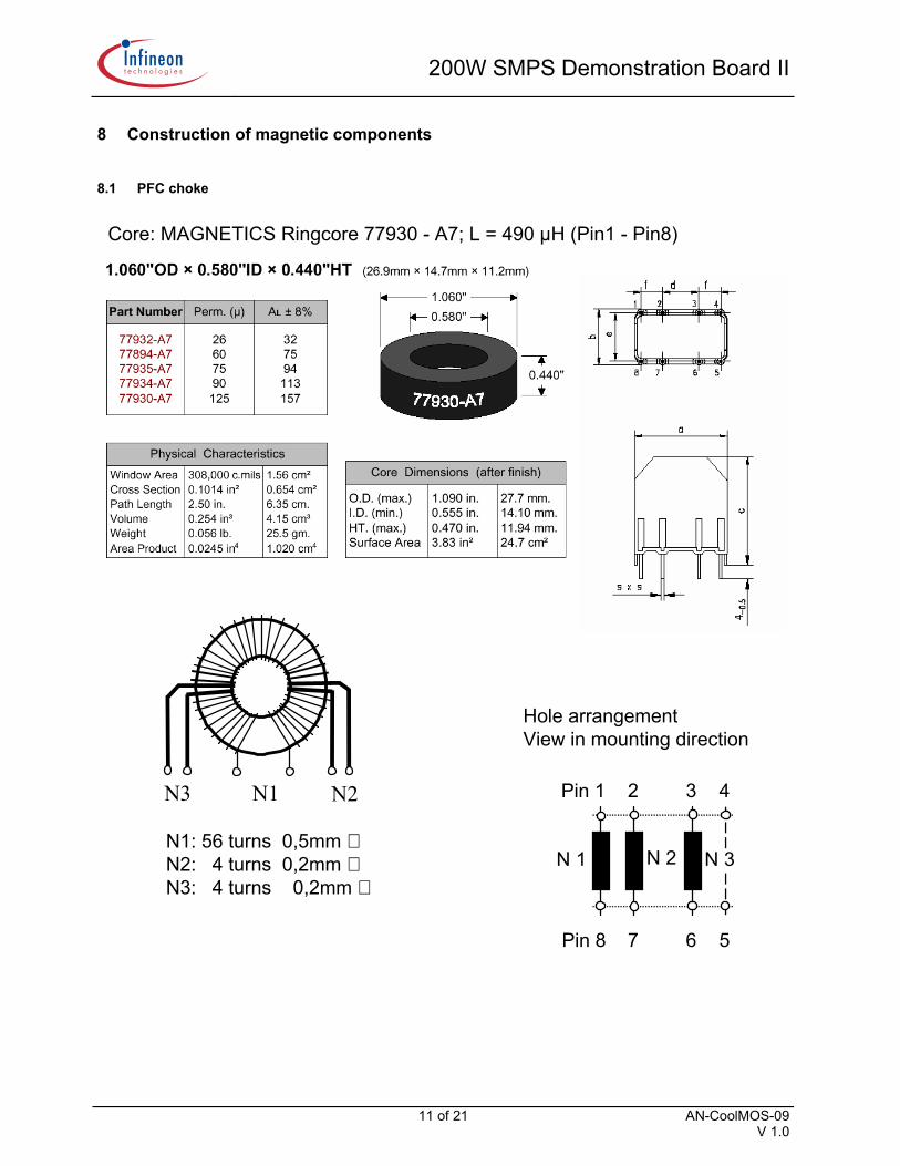
8.1 PFC choke
Core: MAGNETICS Ringcore 77930 - A7; L = 490 µH (Pin1 - Pin8)
N1: 56 turns 0,5mm ∅N2: 4 turns 0,2mm ∅N3: 4 turns 0,2mm ∅
Hole arrangementView in mounting direction
N3 N1 N2 Pin 1 2 43
Pin 8 7 6 5
N 1 N 2 N 3
200W SMPS Demonstration Board II
12 of 21 AN-CoolMOS-09 V 1.0
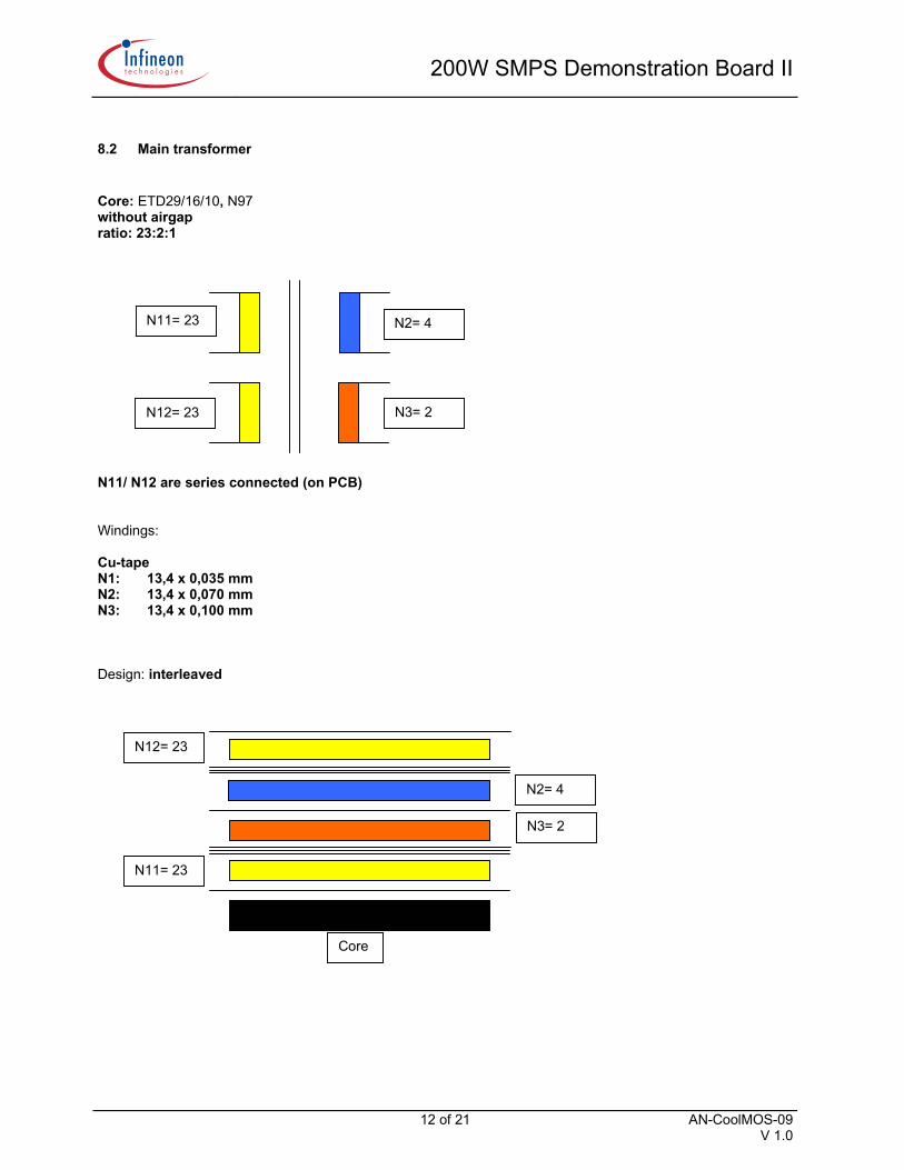
8.2 Main transformer Core: ETD29/16/10, N97 without airgap ratio: 23:2:1 N11/ N12 are series connected (on PCB) Windings: Cu-tape N1: 13,4 x 0,035 mm N2: 13,4 x 0,070 mm N3: 13,4 x 0,100 mm Design: interleaved
N11= 23
N12= 23
N2= 4
N3= 2
N11= 23
N12= 23
N3= 2
N2= 4
Core
200W SMPS Demonstration Board II
13 of 21 AN-CoolMOS-09 V 1.0
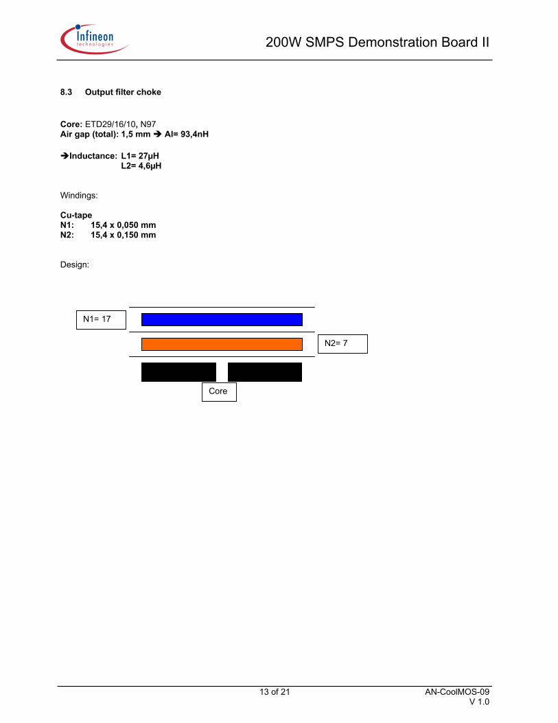
8.3 Output filter choke Core: ETD29/16/10, N97 Air gap (total): 1,5 mm Al= 93,4nH
Inductance: L1= 27µH L2= 4,6µH Windings: Cu-tape N1: 15,4 x 0,050 mm N2: 15,4 x 0,150 mm Design:
N1= 17
N2= 7
Core
200W SMPS Demonstration Board II
14 of 21 AN-CoolMOS-09 V 1.0
9 PCB Layout
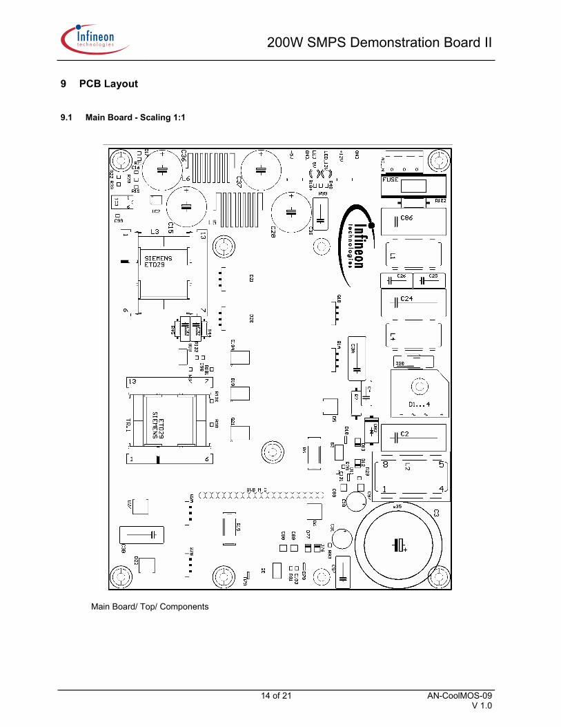
9.1 Main Board - Scaling 1:1
Main Board/ Top/ Components
200W SMPS Demonstration Board II
15 of 21 AN-CoolMOS-09 V 1.0
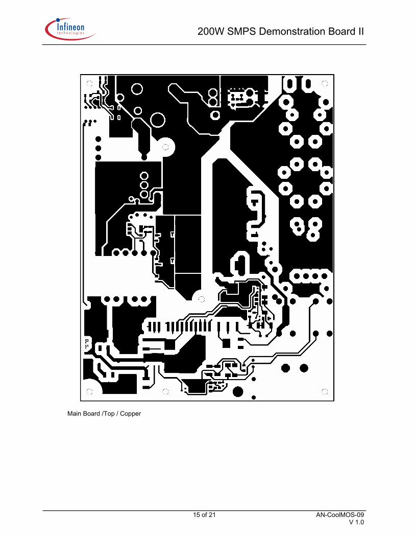
Main Board /Top / Copper
200W SMPS Demonstration Board II
16 of 21 AN-CoolMOS-09 V 1.0
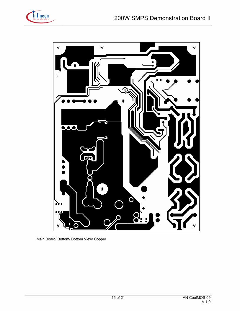
Main Board/ Bottom/ Bottom View/ Copper
200W SMPS Demonstration Board II
17 of 21 AN-CoolMOS-09 V 1.0
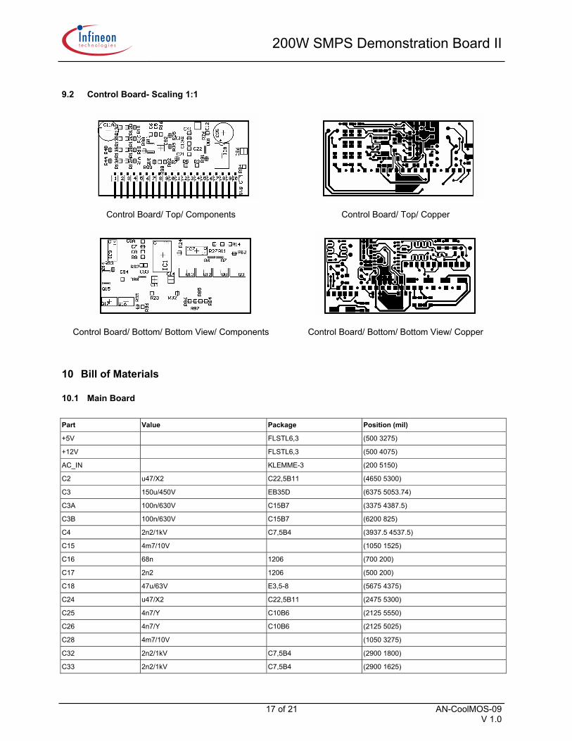
9.2 Control Board- Scaling 1:1
Control Board/ Top/ Components
Control Board/ Top/ Copper
Control Board/ Bottom/ Bottom View/ Components
Control Board/ Bottom/ Bottom View/ Copper
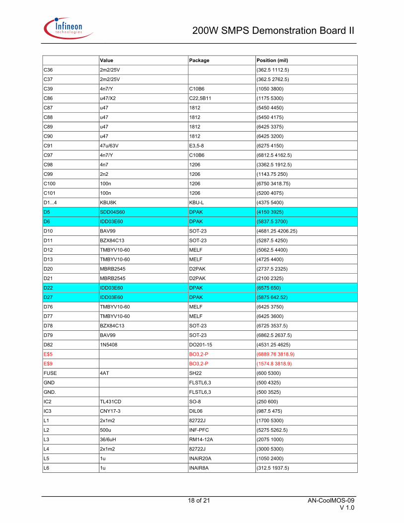
10 Bill of Materials
10.1 Main Board
Part Value Package Position (mil)
+5V FLSTL6,3 (500 3275)
+12V FLSTL6,3 (500 4075)
AC_IN KLEMME-3 (200 5150)
C2 u47/X2 C22,5B11 (4650 5300)
C3 150u/450V EB35D (6375 5053.74)
C3A 100n/630V C15B7 (3375 4387.5)
C3B 100n/630V C15B7 (6200 825)
C4 2n2/1kV C7,5B4 (3937.5 4537.5)
C15 4m7/10V (1050 1525)
C16 68n 1206 (700 200)
C17 2n2 1206 (500 200)
C18 47u/63V E3,5-8 (5675 4375)
C24 u47/X2 C22,5B11 (2475 5300)
C25 4n7/Y C10B6 (2125 5550)
C26 4n7/Y C10B6 (2125 5025)
C28 4m7/10V (1050 3275)
C32 2n2/1kV C7,5B4 (2900 1800)
C33 2n2/1kV C7,5B4 (2900 1625)
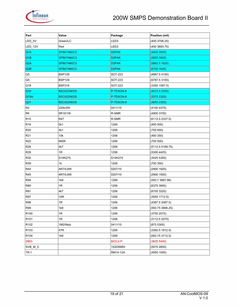
200W SMPS Demonstration Board II
18 of 21 AN-CoolMOS-09 V 1.0
Value Package Position (mil)
C36 2m2/25V (362.5 1112.5)
C37 2m2/25V (362.5 2762.5)
C39 4n7/Y C10B6 (1050 3800)
C86 u47/X2 C22,5B11 (1175 5300)
C87 u47 1812 (5450 4450)
C88 u47 1812 (5450 4175)
C89 u47 1812 (6425 3375)
C90 u47 1812 (6425 3200)
C91 47u/63V E3,5-8 (6275 4150)
C97 4n7/Y C10B6 (6812.5 4162.5)
C98 4n7 1206 (3362.5 1912.5)
C99 2n2 1206 (1143.75 250)
C100 100n 1206 (6750 3418.75)
C101 100n 1206 (5200 4075)
D1...4 KBU8K KBU-L (4375 5400)
D5 SDD04S60 DPAK (4150 3925)
D6 IDD03E60 DPAK (5837.5 3700)
D10 BAV99 SOT-23 (4681.25 4206.25)
D11 BZX84C13 SOT-23 (5287.5 4250)
D12 TMBYV10-60 MELF (5062.5 4400)
D13 TMBYV10-60 MELF (4725 4400)
D20 MBRB2545 D2PAK (2737.5 2325)
D21 MBRB2545 D2PAK (2100 2325)
D22 IDD03E60 DPAK (6575 650)
D27 IDD03E60 DPAK (5875 642.52)
D76 TMBYV10-60 MELF (6425 3750)
D77 TMBYV10-60 MELF (6425 3600)
D78 BZX84C13 SOT-23 (6725 3537.5)
D79 BAV99 SOT-23 (6862.5 2637.5)
D82 1N5408 DO201-15 (4531.25 4625)
E$5 BO3,2-P (6889.76 3818.9)
E$9 BO3,2-P (1574.8 3818.9)
FUSE 4AT SH22 (600 5300)
GND FLSTL6,3 (500 4325)
GND. FLSTL6,3 (500 3525)
IC2 TL431CD SO-8 (250 600)
IC3 CNY17-3 DIL06 (987.5 475)
L1 2x1m2 82722J (1700 5300)
L2 500u INF-PFC (5275 5262.5)
L3 36/6uH RM14-12A (2075 1000)
L4 2x1m2 82722J (3000 5300)
L5 1u INAIR20A (1050 2400)
L6 1u INAIR8A (312.5 1937.5)
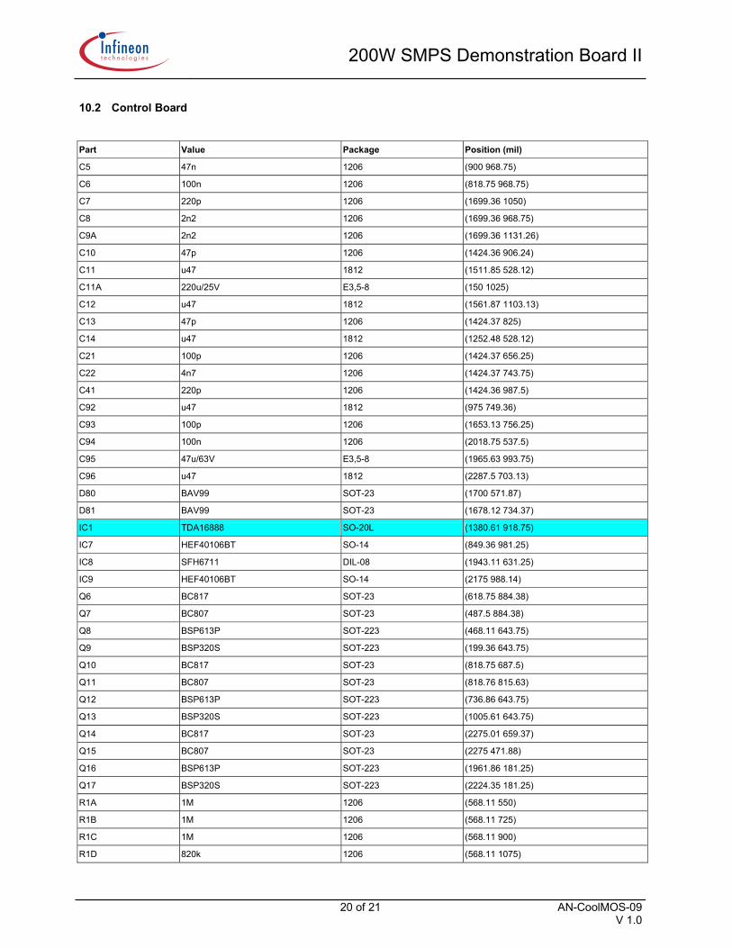
200W SMPS Demonstration Board II
19 of 21 AN-CoolMOS-09 V 1.0
Part Value Package Position (mil)
LED_5V Green/LC LED3 (400 3706.25)
LED_12V Red LED3 (400 3893.75)
Q1A SPB07N60C3 D2PAK (3400 3925)
Q1B SPB07N60C3 D2PAK (2650 3925)
Q2A SPB07N60C3 D2PAK (5862.5 1625)
Q2B SPB07N60C3 D2PAK (6700 1625)
Q3 BSP129 SOT-223 (4887.5 4100)
Q5 BSP129 SOT-223 (6787.5 3100)
Q18 BSP318 SOT-223 (3350 1587.5)
Q19 BSC022N03S P-TDSON-8 (4012.5 2325)
Q19A BSC022N03S P-TDSON-8 (3375 2325)
Q21 BSC022N03S P-TDSON-8 (4650 2325)
R2 220k/2W 0411/15 (4100 4375)
R6 0R15/1W R-SMR (4900 3700)
R15 R47 R-SMR (6112.5 2337.5)
R19 5k1 1206 (450 500)
R20 5k1 1206 (700 650)
R21 10k 1206 (450 350)
R22 680R 1206 (700 500)
R28 4k7 1206 (5112.5 4168.75)
R29 1R 1206 (5300 4425)
R30 S14K275 S14K275 (3425 5300)
R39 1k 1206 (700 350)
R44 4R7/0,6W 0207/10 (2900 1925)
R45 4R7/0,6W 0207/10 (2900 1500)
R48 1k8 1206 (593.7 3897.98)
R80 1R 1206 (6375 3950)
R81 4k7 1206 (6750 3325)
R97 10R 1206 (3550 1712.5)
R98 1R 1206 (4387.5 2087.5)
R99 1k8 1206 (593.75 3806.25)
R100 1R 1206 (3750 2075)
R101 1R 1206 (3112.5 2075)
R102 1M2/Netz 0411/15 (875 5300)
R103 47R 1206 (3362.5 1812.5)
R104 1k8 1206 (593.75 3712.5)
S$63 BO3,2-P (3825 5400)
SVB_M_C 1X20SMDI (5575 2850)
TR.1 RM14-12A (4550 1000)
200W SMPS Demonstration Board II
20 of 21 AN-CoolMOS-09 V 1.0
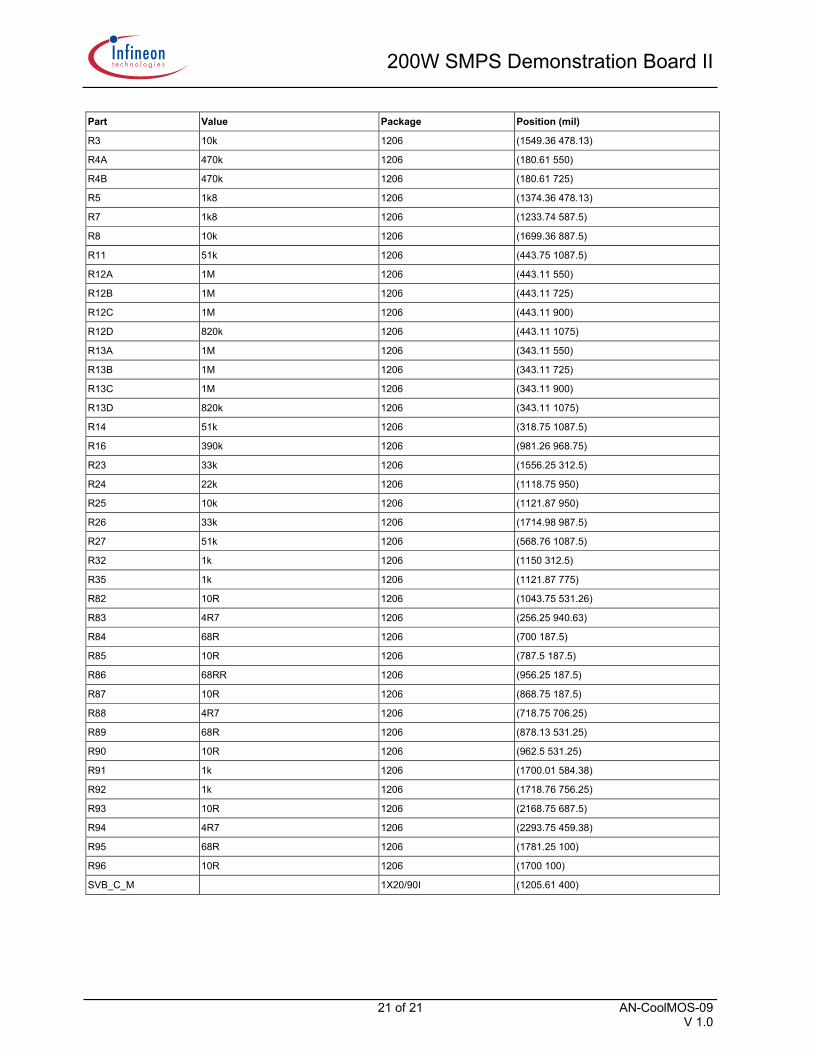
10.2 Control Board Part Value Package Position (mil)
C5 47n 1206 (900 968.75)
C6 100n 1206 (818.75 968.75)
C7 220p 1206 (1699.36 1050)
C8 2n2 1206 (1699.36 968.75)
C9A 2n2 1206 (1699.36 1131.26)
C10 47p 1206 (1424.36 906.24)
C11 u47 1812 (1511.85 528.12)
C11A 220u/25V E3,5-8 (150 1025)
C12 u47 1812 (1561.87 1103.13)
C13 47p 1206 (1424.37 825)
C14 u47 1812 (1252.48 528.12)
C21 100p 1206 (1424.37 656.25)
C22 4n7 1206 (1424.37 743.75)
C41 220p 1206 (1424.36 987.5)
C92 u47 1812 (975 749.36)
C93 100p 1206 (1653.13 756.25)
C94 100n 1206 (2018.75 537.5)
C95 47u/63V E3,5-8 (1965.63 993.75)
C96 u47 1812 (2287.5 703.13)
D80 BAV99 SOT-23 (1700 571.87)
D81 BAV99 SOT-23 (1678.12 734.37)
IC1 TDA16888 SO-20L (1380.61 918.75)
IC7 HEF40106BT SO-14 (849.36 981.25)
IC8 SFH6711 DIL-08 (1943.11 631.25)
IC9 HEF40106BT SO-14 (2175 988.14)
Q6 BC817 SOT-23 (618.75 884.38)
Q7 BC807 SOT-23 (487.5 884.38)
Q8 BSP613P SOT-223 (468.11 643.75)
Q9 BSP320S SOT-223 (199.36 643.75)
Q10 BC817 SOT-23 (818.75 687.5)
Q11 BC807 SOT-23 (818.76 815.63)
Q12 BSP613P SOT-223 (736.86 643.75)
Q13 BSP320S SOT-223 (1005.61 643.75)
Q14 BC817 SOT-23 (2275.01 659.37)
Q15 BC807 SOT-23 (2275 471.88)
Q16 BSP613P SOT-223 (1961.86 181.25)
Q17 BSP320S SOT-223 (2224.35 181.25)
R1A 1M 1206 (568.11 550)
R1B 1M 1206 (568.11 725)
R1C 1M 1206 (568.11 900)
R1D 820k 1206 (568.11 1075)
200W SMPS Demonstration Board II
21 of 21 AN-CoolMOS-09 V 1.0
Part Value Package Position (mil)
R3 10k 1206 (1549.36 478.13)
R4A 470k 1206 (180.61 550)
R4B 470k 1206 (180.61 725)
R5 1k8 1206 (1374.36 478.13)
R7 1k8 1206 (1233.74 587.5)
R8 10k 1206 (1699.36 887.5)
R11 51k 1206 (443.75 1087.5)
R12A 1M 1206 (443.11 550)
R12B 1M 1206 (443.11 725)
R12C 1M 1206 (443.11 900)
R12D 820k 1206 (443.11 1075)
R13A 1M 1206 (343.11 550)
R13B 1M 1206 (343.11 725)
R13C 1M 1206 (343.11 900)
R13D 820k 1206 (343.11 1075)
R14 51k 1206 (318.75 1087.5)
R16 390k 1206 (981.26 968.75)
R23 33k 1206 (1556.25 312.5)
R24 22k 1206 (1118.75 950)
R25 10k 1206 (1121.87 950)
R26 33k 1206 (1714.98 987.5)
R27 51k 1206 (568.76 1087.5)
R32 1k 1206 (1150 312.5)
R35 1k 1206 (1121.87 775)
R82 10R 1206 (1043.75 531.26)
R83 4R7 1206 (256.25 940.63)
R84 68R 1206 (700 187.5)
R85 10R 1206 (787.5 187.5)
R86 68RR 1206 (956.25 187.5)
R87 10R 1206 (868.75 187.5)
R88 4R7 1206 (718.75 706.25)
R89 68R 1206 (878.13 531.25)
R90 10R 1206 (962.5 531.25)
R91 1k 1206 (1700.01 584.38)
R92 1k 1206 (1718.76 756.25)
R93 10R 1206 (2168.75 687.5)
R94 4R7 1206 (2293.75 459.38)
R95 68R 1206 (1781.25 100)
R96 10R 1206 (1700 100)
SVB_C_M 1X20/90I (1205.61 400)