2010 annual report volume xxviii march 2011
TRANSCRIPT

Proprietary Release subject to the terms and conditions of the Precision Engineering Center Membership Agreement
and North Carolina State University Office of Technology Transfer nondisclosure agreements.
PRECISION
ENGINEERING
CENTER
2010 ANNUAL REPORT
VOLUME XXVIII
March 2011
Sponsors: Lockheed Martin Corporation
Minnesota Mining & Manufacturing Company (3M)
National Institutes of Health (NIH)
National Science Foundation (NSF)
Strategic Research Initiatives (NCSU)
Vistakon, Division of Johnson & Johnson Vision Care, Inc.
Faculty: Thomas Dow
Ronald Scattergood
David Muddiman
Jeff Eischen
Dave Hinks
Keith Beck
Graduate Students: Brandon Lane Guillaume Robichaud
Erik Zdanowicz Zachary Marston
Undergraduate Students: Darrell LaBarbera Neil VonHolle
Staff:
Kenneth Garrard
Alexander Sohn
Monica Ramanath
Consultants:
Karl J. Falter
Amir Pirzadeh, Tisfoon Ulterior Systems
Andy Fanning, Fanning Technical Services
Robert Smythe, R. A. Smythe, LLC

Table of Contents
Summary i
1. Polaris 3D Development
Alex Sohn and Ken Garrard 1
2. Measuring Transparent Surfaces with Polaris 3D
Alex Sohn 9
3. Flora II Upgrades and Performance Testing
Thomas Dow and Ken Garrard 17
4. Integrated Prescan Optics for Laser Printers
Alex Sohn and Ken Garrard 29
5. Fabrication and Testing of an Air Amplifier as a Focusing Device for Electrospray
Ionization Mass Spectrometry
Guillaume Robichaud, Thomas Dow, and Alex Sohn 39
6. Effects of Varying EVAM Parameters on Chemical Tool Wear
Brandon Lane, Thomas Dow, and Ronald Scattergood 53
7. Visualization of Chip Shape and Machining Forces
Darrell LaBarbera and Thomas Dow 73
8. Ultrasonic Vibration Assisted Machining
Neil VonHolle, Brandon Lane, and Thomas Dow 81
9. Nanocoining and Optical Features
Erik Zdanowicz, Thomas Dow, and Ronald Scattergood 89
Personnel 110
Graduates of the PEC 119
Academic Program 127
Publications 134

Proprietary Release subject to the terms and conditions of the Precision Engineering Center Membership Agreement
and North Carolina State University Office of Technology Transfer nondisclosure agreements.
i
SUMMARY
The goals of the Precision Engineering Center are: 1) to develop new technology in the areas of
precision metrology, actuation, manufacturing and assembly; and 2) to train a new generation of
engineers and scientists with the background and experience to transfer this technology to
industry. Because the problems related to precision engineering originate from a variety of
sources, significant progress can only be achieved by applying a multidisciplinary approach; one
in which the faculty, students, staff and sponsors work together to identify important research
issues and find the optimum solutions. Such an environment has been created and nurtured at
the PEC for 29 years and the 100+ graduates attest to the quality of the results.
The 2010 Annual Report summarizes the progress over the past year by the faculty, students and
staff in the Precision Engineering Center. During the past year, this group included 3 faculty, 7
graduate students, 2 undergraduate students, 2 full-time technical staff members and 1
administrative staff member. This diverse group of scientists and engineers provides a wealth of
experience to address precision engineering problems. The format of this Annual Report
separates the research effort into individual projects but there is significant interaction that
occurs among the faculty, staff and students. Weekly seminars by the students and faculty
provide information exchange and feedback as well as practice in technical presentations.
Teamwork and group interactions are a hallmark of research at the PEC and this contributes to
both the quality of the results as well as the education of the graduates.
A brief abstract follows for each of the projects and the details of the progress in each is
described in the remainder of the report.
1. Polaris 3D Development
The development of the Polaris 3D, a non-contacting spherical coordinate system measuring
machine, has continued with further improvements in probing and error correction. A new
chromatic aberration optical probe using an LED light source with adjustable intensity output
has provided more flexibility to measure a wider variety of surface materials while
improving signal-to-noise ratio. New techniques for compensating for spindle radial error
motion and alignment errors between the part and measurement spindle are discussed. .
2. Measuring Transparent Surfaces with Polaris 3D
Techniques for measuring transparent surfaces have been explored on Polaris 3D. The low
reflectivity of such surfaces presents unique challenges for finding the surface, but with
advanced optical probe hardware and new techniques, accurate measurement of glass,
acrylic, and other transparent surfaces are possible. In addition to measuring the shape of the

Proprietary Release subject to the terms and conditions of the Precision Engineering Center Membership Agreement
and North Carolina State University Office of Technology Transfer nondisclosure agreements.
ii
first surface, thickness measurement looking through to the second surface was explored.
While such a measurement is possible, details related to the index of refraction and surface
shape introduce difficulties that will make implementation very difficult. The solution that
solves the issue is to flip the part over and measure the other side.
3. Flora II Upgrades and Performance Testing
The Fast Long Range Actuator (FLORA II) was developed to machine non-rotationally
symmetric surfaces on a ultra-precision lathe with a diamond tool. FLORA was designed to
have a much longer range than piezoelectric based fast tool servos and significantly higher
bandwidth than a slow slide servo. Excellent actuator performance was previously
demonstrated, but the user interface needed a major overhaul to improve its efficacy. For
this reason, the actuator and its controls have been upgraded and improved and FLORA II is
now fully integrated into the diamond turning machine. Specifically, the safety circuits,
control system and user interface have been re-engineered and software has been added to
translate a surface shape into the motion program needed to machine that surface.
4. Integrated Prescan Optics for Laser Printers
An integrated two-element reflective optical system for a laser prescan unit has been
designed and fabricated. The optical system was machined from a single piece eliminating
the need for assembly and alignment of the two mirrors. However, in their correct
orientation in the optical system, neither mirror is rotationally symmetric about any axis. The
FLORA II fast tool servo in conjunction with an ultra-precision DTM was used to create the
mirror surfaces. Matlab software was developed to decompose a multi-element optical
system into a best fit asphere (followed by the DTM) and a non-rotationally symmetric
surface (followed by the FLORA II). The shape of the resulting surfaces as measured with
the Polaris 3D is presented.
5. Development of an Air Amplifier as a Focusing Device for Electrospray Ionization Mass
Spectrometry
Mass spectrometry (MS) is an analytical method used to identify molecules and complex
proteins based on their mass-to-charge ratio. It is extensively used in analytical chemistry,
cancer research, drug testing, explosive detection, etc. However, to be measured, molecules
first must be transferred into gas phase and ionized. Electrospray ionization is the dominant
technique currently used but only about 1% of ions generated will be measured by the mass
spectrometer. This is mainly due to the loss of ions between electrospray source and the
instrument inlet due to their charge repulsion and the lack of a focusing method. This NIH
funded project is a joint effort combining precision machining and computational fluid
dynamics, an aerodynamic focusing device has been designed, fabricated and demonstrated.

Proprietary Release subject to the terms and conditions of the Precision Engineering Center Membership Agreement
and North Carolina State University Office of Technology Transfer nondisclosure agreements.
iii
6. Effects of Varying EVAM Parameters on Chemical Tool Wear
Reported benefits of applying micrometer-scale vibration to a diamond tool during precision
diamond turning (DT) include a decrease in machining forces and wear of the diamond tool.
Despite two decades of elliptical vibration-assisted machining (EVAM) research, few have
addressed the details and reason for the reduced tool wear. A chemical tool wear model is
presented to relate conventional DT tool wear to machining temperatures estimated from
finite element models (FEM). This wear model is then applied to FE simulations of EVAM
for different workpiece velocities, frequencies, and ellipse shapes. EVAM experiments
varying frequency were then conducted and surface finish and tool wear were measured.
Optical surface finish was achieved machining low carbon steel but tool edge measurements
did not collaborate the reduced wear expected.
7. Visualization of Chip Shape and Machining Forces
The goal is this project was simultaneously measurement of cutting forces and chip shape
during diamond turning of aluminum and steel workpieces. Measuring these two parameters
have been done separately by a number of investigators, but performing them simultaneously
will provide increased understanding of the chip pickup problem. Chip pickup occurs during
machining of steel when the workpiece material becomes attached to the cutting tool
resulting in higher tool forces and poor surface finish. Cutting and thrust forces were
measured using a 3-axis load cell and video images of the chip through a microscope were
recorded with depths ranging from from 7 to 25 μm. The chip images had sufficient visual
clarity to see the chip formation and relate it to the forces measured.
8. Ultrasonic Vibration Assisted Machining
An ultrasonic elliptical vibration assisted machining (EVAM) device operating at 25 KHz
was designed and tested by a summer undergraduate student funded by NSF. This device
utilized a piezoelectric resonator called a sonotrode coupled to a parabolic horn to drive the
diamond tool in an elliptical path. The resonant frequency and vibrational tool path was
determined using finite element modeling and corroborated using an infrared displacement
sensor. The device was used to machine 6061-T6 aluminum and C360 brass workpieces.
The compliant mounting of the sonotrode and issues related to tool motion direction resulted
in poor surface finish. However, the effort indicated the suitability of this type of actuator to
increase the speed of the EVAM experiments above the 1-4 KHz range of the Ultramill.
9. Nanocoining of Optical Features
The goal of this research is to create surfaces with features smaller than the wavelength of
light using a process called nanocoining. Nanocoining uses a nanostructured diamond die to
imprint sub-micrometer features onto the surface of a mold. Because the die is small and the
desired size of the mold is large, it must be done at very high speed – on the order of 50 KHz.

Proprietary Release subject to the terms and conditions of the Precision Engineering Center Membership Agreement
and North Carolina State University Office of Technology Transfer nondisclosure agreements.
iv
The physical process of the nano-indentation is being investigated to understand how
materials behave at the nano-scale and how multiple indentations will influence each other.
A functional system will be produced by creating experimental indents at slow speed and
comparing them to FEA results while simultaneously designing a resonant structure capable
of achieving the required displacements at ultrasonic speeds. The ultrasonic actuator along
with the ability to create nanostructured features are the key elements to producing optical
quality surfaces efficiently.
1 Proprietary Release subject to the terms and conditions of the Precision Engineering Center Membership Agreement
and North Carolina State University Office of Technology Transfer nondisclosure agreements.
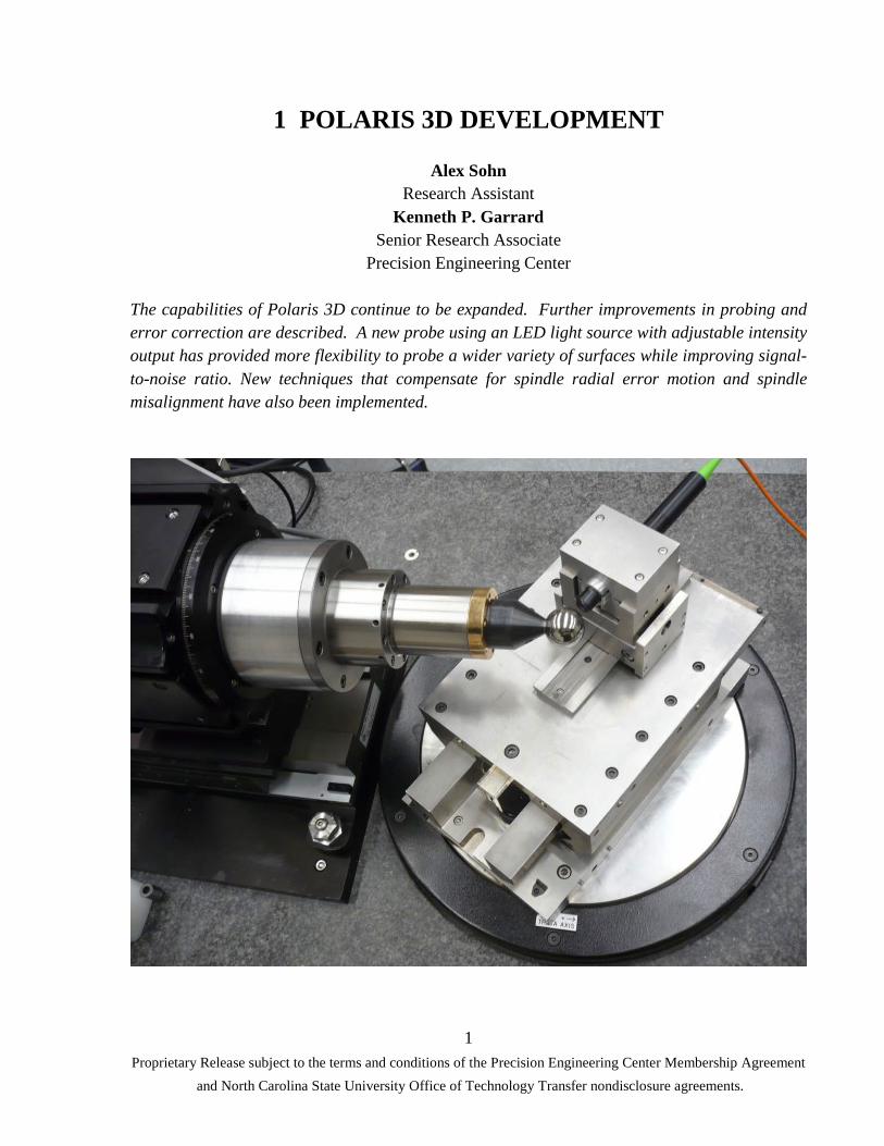
1 POLARIS 3D DEVELOPMENT
Alex Sohn Research Assistant
Kenneth P. Garrard Senior Research Associate
Precision Engineering Center
The capabilities of Polaris 3D continue to be expanded. Further improvements in probing and error correction are described. A new probe using an LED light source with adjustable intensity output has provided more flexibility to probe a wider variety of surfaces while improving signal-to-noise ratio. New techniques that compensate for spindle radial error motion and spindle misalignment have also been implemented.

2 Proprietary Release subject to the terms and conditions of the Precision Engineering Center Membership Agreement
and North Carolina State University Office of Technology Transfer nondisclosure agreements.
1.1 INTRODUCTION The profilometer Polaris 3D measures curved surfaces in a spherical coordinate system. It was first developed as a 2D measuring machine with a contacting probe but over the past 2 years has been upgraded to measure 3D surfaces with non-contacting optical probe. The profilometer has a pair of axes that sweep the optical probe over the surface and a second set to position and rotate the part. Errors for each slide and spindle have been measured and compensation algorithms developed. Alignment techniques have also been developed to establish the origin of each axis with respect to the other axes. These algorithms for compensation of repeatable error motions and misalignment of axes were previously developed [1] but have now been improved and implemented in either the controller or the post-measurement data analysis software. 1.2 PROBE EVALUATION A new Chromatic Aberration (CA) system (CHRocodile S) was loaned to the PEC by Precitec for evaluation. It used a LED light source and came with optical pens that have 300 µm and 600 µm range. They were tested along with the Stil CHR150-N CA system with a 300 µm range pen and a halogen light source owned by the PEC. A 300 µm range CHR 150-N has since been purchased by the PEC and has replaced the Stil system. 1.2.1 ANGLE OF INCIDENCE DEPENDENCE All of the probes had some variation in distance measurement as a function of angle of incidence. The test for this error involves the use of a 12.7 mm diameter brass diamond turned flat with a flatness of 250 nm (PV). Once the probe has been aligned, the test flat is moved 50 µm from the origin with the R axis and the rotary table (θ axis) is rotated. Rotation produces a displacement, ρ, according to Equation (1).
10.05cos
ρθ
=
(1)
With probe tracking disabled, data is collected while θ is rotated. The difference between the measured probe displacement and the displacement calculated from Equation (1) gives the measurement error as shown in Figure 1.

3 Proprietary Release subject to the terms and conditions of the Precision Engineering Center Membership Agreement
and North Carolina State University Office of Technology Transfer nondisclosure agreements.
Figure 1. Measurement error for three probes vs. angle of incidence. This error not only impacts measurements when the angle of incidence is significant, but also has an impact on the original probe alignment method [2]. This discovery has been the main motivation behind the improved probe alignment method (see Section 1.3.2) using a spherical artifact instead of a reference flat. 1.2.2 PROBE NOISE Data was collected at 1.1 kHz for six seconds for each probe while incident on a brass flat with probe tracking disabled. RMS noise measurements from this test are shown in Table 1 for two probe manufacturers (Precitec and Stil) and two probe ranges (0-300 µm and 0-600 µm). The measurements reveal a substantially lower noise level for the Precitec probes that use an LED source.
Table 1. CA Probe Noise Probe Precitec CHRocodile S
600 µm range Precitec CHRocodile S
300 µm range Stil CHR150-N 300 µm range
RMS noise (nm) 27 24 66

4 Proprietary Release subject to the terms and conditions of the Precision Engineering Center Membership Agreement
and North Carolina State University Office of Technology Transfer nondisclosure agreements.
1.3 ERROR COMPENSATION 1.3.1 RADIAL ERROR COMPENSATION OF THE SPINDLE While specified to be less than ±100 nm at the spindle face, the combination of a large measurement offset from this face and a significant tilt error of the part spindle (φ axis) result in error motions in excess of 1 µm at the part location. The greatest impact of these radial error motions is in the x (horizontal) direction of the machine. This x-error (eφx), as measured by a capacitance gauge on a precision steel ball is shown in Figure 2 (left) along with a best fit 6th order Fourier series. The curve fit is used to implement the compensation. The residual from this curve fit is shown in Figure 3 (right) and fits the error to ± 150 nm.
Figure 2. Radial error motion in the x direction of more than 1 µm with a best-fit Fourier series
(left) and residual x-direction radial error after compensation (right)
Radial error motion is compensated by modifying R axis measured values as a function of the best-fit Fourier series and the rotary table angle (θ) using Equation (2). sinR xe eϕ ϕ θ= (2)
Equation (2) is subtracted from the each recorded R axis position to compensate for the radial error motion of the part spindle. 1.3.2 PROBE ALIGNMENT Alignment of the optical probe with the R axis and rotary table (θ) is critical to the analysis of a measurement. The goal is to have the probe zero exactly at the origin of the polar coordinate

5 Proprietary Release subject to the terms and conditions of the Precision Engineering Center Membership Agreement
and North Carolina State University Office of Technology Transfer nondisclosure agreements.
system formed by this linear and rotary axis pair. However perfect alignment is not necessary as the misalignment can be compensated in the analysis if the offset is known. A technique for measuring this misalignment with a reference flat was developed for the 2D Polaris machine [3] and further improvements were made for Polaris 3D [4]. However in light of angular probe dependence discussed above, a more robust technique has been developed. The technique developed for the 2D system made use of the relationship between a radial (i.e., R direction) offset, angle, and observed displacement as given in Equation (1). The sensitivity of the so-called ρ error to probe noise and the angular dependence discussed limit the technique of using a reference flat. Instead a reference sphere is used to directly compare the R direction offset with the sphere radius. This could be done by taking two data points on opposite sides of the sphere and thus directly measuring the diameter of the artifact. A better technique is to measure the rotating sphere through 180° degrees of motion of the θ axis and perform a least squares fit to the result. The difference between the best fit radius and the known sphere size is the alignment offset. Note that the “reversal” technique for eliminating artifact errors is inherent in the data when measuring from equator to pole to equator as the sphere rotates. Therefore, this runout of the part on the spindle and any horizontal misalignment of the two rotating axes are canceled. 1.3.3 HORIZONTAL ALIGNMENT OF THE ROTARY AXES The two rotating axes (φ and θ) must intersect at a right angle for the Polaris machine to form a true spherical coordinate system. However a small error can be compensated in the analysis code if the error can be accurately measured. When measuring a sphere on one side, say the pole toward the equator at +90°, a horizontal offset will make the sphere appear too small if the offset is positive and too large if it is negative. At the equator, the discrepancy in the radius seen by the probe of a known sphere or cylinder is proportional to the horizontal alignment offset. So this error can also be determined from two runout measurements of a spherical artifact (or cylinder) from rotary table orientations 180 degrees apart. The φ-θ alignment error is then given by Equation (3), where r+90 and r-90 are the two best fit radii determined from the runout measurements that were generated in the new technique for probe alignment discussed above.
90 90
2 2r reϕθ
+ −= − (3)
Compensation for this error in subsequent measurements is done with new values for radial (R’) position and angular position (θ’) as shown in Equations (4) and (5).
2 2 2 cos2
R R e e rϕθ ϕθπθ ′ = + − +
(4)

6 Proprietary Release subject to the terms and conditions of the Precision Engineering Center Membership Agreement
and North Carolina State University Office of Technology Transfer nondisclosure agreements.
2 2 2
2R R e
e Rϕθ
ϕθ
θ′− −
′ =′−
(5)
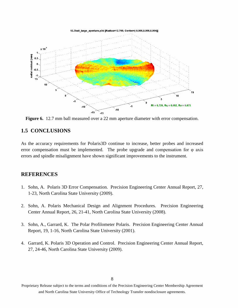
1.4 RESULTS Updates to the error measurement and compensation techniques for correcting φ axis radial spindle error motions and spindle axis misalignment on Polaris 3D have been completed to create accurate and repeatable measurements of a variety of surfaces with the CA optical probes. Figures 3 and 4 show measurement residuals for a 12.7 mm radius sphere measured over a small aperture (10 mm diameter) with and without error compensation. Figures 5 and 6 show the measurement residual for a 22 mm diameter measurement aperture of the same sphere. In both cases the best fit radius is within 300 nm of the accepted value of 12.7 mm which has an uncertainty of ±500 nm.
Figure 3. 12.7 mm ball measured over a 10 mm aperture diameter without error compensation.

7 Proprietary Release subject to the terms and conditions of the Precision Engineering Center Membership Agreement
and North Carolina State University Office of Technology Transfer nondisclosure agreements.
Figure 4. 12.7 mm ball measured over a 10 mm aperture diameter with error compensation.
Figure 5. 12.7 mm ball measured over a 22 mm aperture diameter without error compensation.
8 Proprietary Release subject to the terms and conditions of the Precision Engineering Center Membership Agreement
and North Carolina State University Office of Technology Transfer nondisclosure agreements.
Figure 6. 12.7 mm ball measured over a 22 mm aperture diameter with error compensation.
1.5 CONCLUSIONS As the accuracy requirements for Polaris3D continue to increase, better probes and increased error compensation must be implemented. The probe upgrade and compensation for φ axis errors and spindle misalignment have shown significant improvements to the instrument. REFERENCES 1. Sohn, A. Polaris 3D Error Compensation. Precision Engineering Center Annual Report, 27,
1-23, North Carolina State University (2009).
2. Sohn, A. Polaris Mechanical Design and Alignment Procedures. Precision Engineering Center Annual Report, 26, 21-41, North Carolina State University (2008).
3. Sohn, A., Garrard, K. The Polar Profilometer Polaris. Precision Engineering Center Annual Report, 19, 1-16, North Carolina State University (2001).
4. Garrard, K. Polaris 3D Operation and Control. Precision Engineering Center Annual Report, 27, 24-46, North Carolina State University (2009).

9
Proprietary Release subject to the terms and conditions of the Precision Engineering Center Membership Agreement
and North Carolina State University Office of Technology Transfer nondisclosure agreements.
2 MEASURING TRANSPARENT SURFACES WITH
POLARIS 3D
Alex Sohn
PEC Staff
The measurement of transparent surfaces has been explored on Polaris 3D. The low reflectivity
of transparent surfaces presents some unique challenges but when combined with advanced
probe hardware and techniques, accurate measurement of glass, acrylic, and other transparent
surfaces becomes possible. In addition to first surface measurement, thickness measurement is
explored. Thickness measurement, while possible, introduces additional difficulties that have
made implementation challenging.

10
Proprietary Release subject to the terms and conditions of the Precision Engineering Center Membership Agreement
and North Carolina State University Office of Technology Transfer nondisclosure agreements.
2.1 INTRODUCTION
Reflective optical surfaces have been measured with Polaris3D since its completion in 2008.
Measurement of transparent surfaces using Polaris 3D opens a new field of applications,
particularly in refractive optics measurement. Since the reflectivity of a typical transparent
surface is much lower than a polished reflective surface, an optical probe must either use a more
intense source or be more sensitive. Additionally, while first surface measurements can be made
directly without compensation, there are some complications with respect to adjusting the
sensitivity of the chromatic aberration (CA) probe.
Two different probes were considered, though in the end, only one was found suited to
measuring transparent surfaces and was used for all measurements. Furthermore, it is possible to
measure through transparent surfaces to measure second surfaces or thickness. This, however,
becomes a more complicated endeavor as the optical path of the CA probe is modified by the
first surface. The measurement of the second surface must therefore be compensated for the
influence of the first surface.
2.2 PROBE CONSIDERATIONS
The main difference between measuring reflective and transparent surfaces is that the reflected
intensity from the transparent surface is substantially lower. Compared to polished aluminum,
which has a reflectivity of around 95%, the reflectivity of glass or many optical polymers with
refractive indices of around 1.5 is about 4%. This means that the signal intensity is about 20
times lower when measuring a transparent surface. There are two ways of accommodating this
disparity in intensity: 1) The intensity of the source can be increased or 2)the measured signal
can be collected for a longer time. In the case of the CHRocodile S probing system, the
sampling rate on the probe was reduced from 2 kHz to 320 Hz. This reduction in sampling rate
increases the exposure time of each sample and hence, the measured intensity. Measured
intensity for transparent plastic was typically around 35% at normal incidence (compared to 95%
for specular brass). This was enough to permit probe following to function properly.
The probe used for all transparent surface measurements was the 300 µm range CHRocodile
probe due to its higher sensitivity as compared to the 600 µm range CHRocodile probe or the
300 µm Stil CHR150-N probe.
11
Proprietary Release subject to the terms and conditions of the Precision Engineering Center Membership Agreement
and North Carolina State University Office of Technology Transfer nondisclosure agreements.
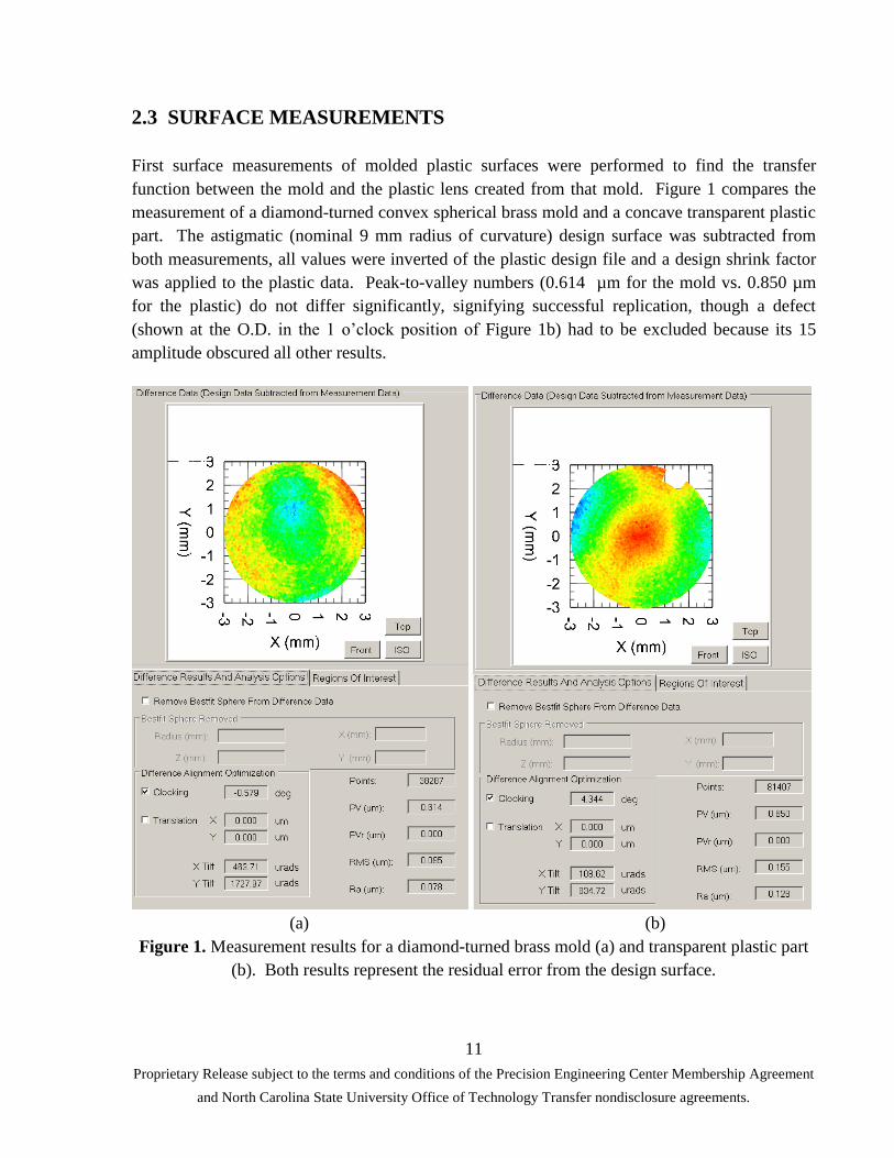
2.3 SURFACE MEASUREMENTS
First surface measurements of molded plastic surfaces were performed to find the transfer
function between the mold and the plastic lens created from that mold. Figure 1 compares the
measurement of a diamond-turned convex spherical brass mold and a concave transparent plastic
part. The astigmatic (nominal 9 mm radius of curvature) design surface was subtracted from
both measurements, all values were inverted of the plastic design file and a design shrink factor
was applied to the plastic data. Peak-to-valley numbers (0.614 µm for the mold vs. 0.850 µm
for the plastic) do not differ significantly, signifying successful replication, though a defect
(shown at the O.D. in the 1 o’clock position of Figure 1b) had to be excluded because its 15
amplitude obscured all other results.
(a) (b)
Figure 1. Measurement results for a diamond-turned brass mold (a) and transparent plastic part
(b). Both results represent the residual error from the design surface.

12
Proprietary Release subject to the terms and conditions of the Precision Engineering Center Membership Agreement
and North Carolina State University Office of Technology Transfer nondisclosure agreements.
2.4 THICKNESS MEASUREMENT
Thickness measurement with CA probes is possible in two different modes: Direct thickness
measurement and indirect. Direct measurement is possible when the apparent thickness of the
measured part lies within the measurement range of the probe and two spectral peaks are
obtained simultaneously as shown in Figure 2. This method is useful in measuring thin windows
or films. Addition of the thickness measurement to a first-surface measurement can produce the
profile of the second measurement.
Figure 2. Direct thickness measuremnt using a CA probe [1].
Indirect thickness measurement is used when the apparent thickness of the part is greater than the
probe’s measurement range. This is the method used for measuring lenses or parts with a
thickness greater than the 300 µm measurement range of the probe used. This indirect method
involves measuring the first surface of the lens and then subtracting the second surface
measurement from this data. Both thickness measurement techniques, however, are complicated
by the fact that measurement of the second surface is perturbed by refraction at the first surface.
The consequence of this is that the perturbation must be compensated.
A section measurement of a polystyrene (n=1.57) lens, for example, revealed the thickness to be
664 µm. With the probe, the thickness was measured at 398 µm. To compensate the impact of
refraction, the aperture must be known, a quantity not given for the probe. The compensation’s
dependence on aperture is shown below and in Figure 3.

13
Proprietary Release subject to the terms and conditions of the Precision Engineering Center Membership Agreement
and North Carolina State University Office of Technology Transfer nondisclosure agreements.
Figure 3. The measured thickness, t0 is perturbed by refraction at the interface between the two
refractive indices, ni and nt.
Snell’s law,
sin sini i t tn n (1)
where ni is the refractive index of the incident medium and nt is that of the transmitted medium.
Likewise, i and t are the incident and transmitted angles, respectively. From the geometry
shown in Figure 3,
0
tan i
d
t (2)
tan t
d
t (3)
where t0 is the measured thickness of the part, t is the actual thickness and d is the aperture
diameter on the surface of the part.
Solving for t0:
1
1 10 tan sin [tan ( / )]t d d t
(4)

14
Proprietary Release subject to the terms and conditions of the Precision Engineering Center Membership Agreement
and North Carolina State University Office of Technology Transfer nondisclosure agreements.
Figure 4. Plot of measured thickness vs. aperture radius given a refractive index of 1.5. The
measured thickness of 0.398 mm is indicated with a line, the intersection with the curve shows
the apparent aperture size.
Equation 4 is evaluated for a range of aperture sizes and plotted in Figure 4 to show how the
measured thickness varies with aperture. This would indicate that the dominant contribution
comes from an aperture of approximately 0.18 mm, though contributions from the entire aperture
means this is more likely just an average. Consequently, the spectrum for measuring through a
planar or quasi-planar surface at normal incidence would be broader than one measured through
air only. This is illustrated by the spectra of the first and second surfaces shown in Figures 5 and
6, respectively. Figure 5 shows the spectrum of a first-surface reflection with a full width at
half-max (FWHM) measurement of approximately 30 nm whereas Figure 6 shows a FWHM of
nearly twice that number.

15
Proprietary Release subject to the terms and conditions of the Precision Engineering Center Membership Agreement
and North Carolina State University Office of Technology Transfer nondisclosure agreements.
Figure 5. Spectrum plot of the signal from the first surface of a transparent plastic part. FWHM
is approximately 30 nm.
Figure 6. Spectrum plot of the signal from the second surface of a transparent plastic part. Note
the broader peak. FWHM is approximately 60 nm.
FWHM
FWHM

16
Proprietary Release subject to the terms and conditions of the Precision Engineering Center Membership Agreement
and North Carolina State University Office of Technology Transfer nondisclosure agreements.
Given that the probe aperture is fixed for any given probe, the ratio of aperture to thickness and,
hence, the angle of incidence and angle of refraction should be constant for quasi-planar
surfaces. Using the plot in Figure 4 to find d/t and Equations 2 and 3 to find i and t a
compensation formula to find t when only t0 is known can be written as:
0
tan
tan
i
t
t t
(5)
or
0t t k , (6)
where k is a correction constant that is measured for each material. In the case of polystyrene, it
is 1.668. Other materials will vary.
This compensation holds only at normal incidence where the radius of curvature of the surface is
large compared to the thickness (~100 times greater). The impact of first surface curvature and
non-normal incidence on thickness measurement still has to be evaluated. It is, however, clear
that the impact on the measured thickness is significant. For example, the center thickness of a
curved plastic window with concentric 1st and 2
nd surface radii of approximately 9 mm was
measured using Polaris 3D. The apparent thickness was measured from both directions with the
result being 434 µm when the convex side was the 1st surface and 407 µm when the concave side
was the 1st surface. This result underscores the importance of finding a compensation algorithm
for this error by virtue of the fact that the difference between the two measurements is 27 µm.
2.4 CONCLUSIONS
The capability for Polaris 3D to measure transparent surfaces was clearly illustrated. First
surface measurements showed that the first surface of a refractive optical element can be
measured just as well as that of a highly reflective element. The only modification to the setup
for measuring transparent surfaces is to lower the CA probe sampling rate by about a factor of
10. Measurement of a second surface transparent part is possible as well, though matters of
refraction at the 1st surface must be dealt with to obtain accurate measurement results for second
surface profile and thickness.
REFERENCES
1. Michelt, Berthold and Schultze, Jochen, The new Chrocodile M4, Glas Ingenieur, 16, pp35-
37 (2006).
17
Proprietary Release subject to the terms and conditions of the Precision Engineering Center Membership Agreement
and North Carolina State University Office of Technology Transfer nondisclosure agreements.
3 FLORA II UPGRADES AND PERFORMANCE
TESTING
Thomas A. Dow
Faculty
Kenneth Garrard
Senior Research Associate
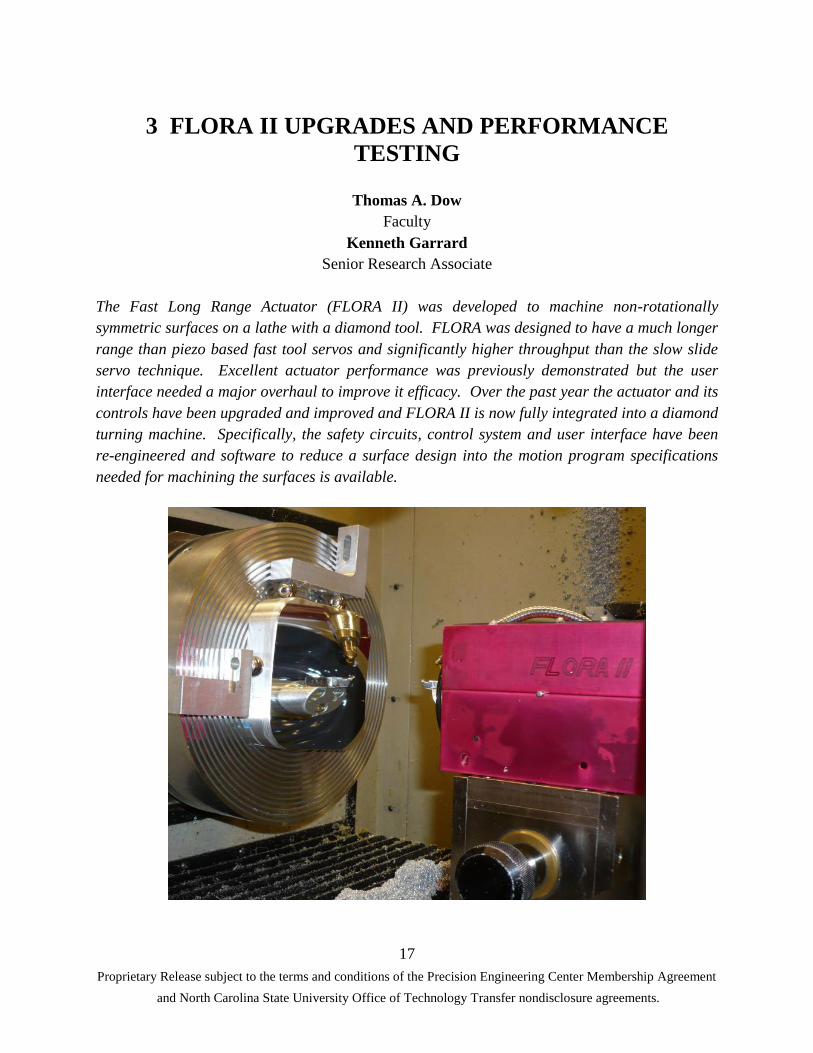
The Fast Long Range Actuator (FLORA II) was developed to machine non-rotationally
symmetric surfaces on a lathe with a diamond tool. FLORA was designed to have a much longer
range than piezo based fast tool servos and significantly higher throughput than the slow slide
servo technique. Excellent actuator performance was previously demonstrated but the user
interface needed a major overhaul to improve it efficacy. Over the past year the actuator and its
controls have been upgraded and improved and FLORA II is now fully integrated into a diamond
turning machine. Specifically, the safety circuits, control system and user interface have been
re-engineered and software to reduce a surface design into the motion program specifications
needed for machining the surfaces is available.

18
Proprietary Release subject to the terms and conditions of the Precision Engineering Center Membership Agreement
and North Carolina State University Office of Technology Transfer nondisclosure agreements.
3.1 INTRODUCTION
The fabrication and measurement of non-rotationally symmetric (freeform) optical surfaces have
long been goals of the PEC. The 3D Polaris discussed in Sections 1 and 2 provides a unique way
to measure these parts which can be fabricated using a variety of fast tool servos powered by
piezoelectric actuators or linear motors.
A project funded by NSF beginning in 2007 was aimed at developing a new servo design. The
goal was a light but rigid mechanical design with a high-performance control system to improve
the surface finish and figure error of the surfaces created. The NSF project was performed by
two graduate students, Qunyi Chen, a PhD graduate, and Erik Zdanowicz, a MS graduate. At the
conclusion, the new actuator design – FLORA II – was working and a DSP based controller
operating at 20 KHz was built to control it. However, as with many of these student projects, the
final result was usable but not user friendly. The effort reported here describes the
improvements to the FLORA II system that enhance the user interface, simplify the operation
and provide a variety of data entry options. Also described are fabrication results for a tilted flat
test part and an off-axis biconic mirror.
3.2 FLORA II IMPROVEMENTS
3.2.1 FLORA II STRUCTURE
Figure 1. FLORA II actuator on micro-height adjustor

19
Proprietary Release subject to the terms and conditions of the Precision Engineering Center Membership Agreement
and North Carolina State University Office of Technology Transfer nondisclosure agreements.
The FLORA II actuator (Fast LOng Range Actuator) developed over the past several years at
the PEC under NSF funding has been used to produce several outstanding optical surfaces over
the past year. The current implementation of this servo is shown in Figure 1. Recent changes
include:
the limit switch system and emergency stop have been improved,
new wiring has been installed,
a new cover to protect the encoder has been fitted and
the counterbalance system has been integrated into the controller.
3.2.2 USER INTERFACE
The PMDi control system has been upgraded with a user interface that provides important new
functionality to start the actuator, find the encoder home reference, communicate with the host
DTM and load data files for freeform surface fabrication. A screen shot of the user interface is
shown in Figure 2.
Figure 2. FLORA II user interface

20
Proprietary Release subject to the terms and conditions of the Precision Engineering Center Membership Agreement
and North Carolina State University Office of Technology Transfer nondisclosure agreements.
The updated graphical user interface (GUI) was a major effort performed by Ken Garrard based
on a design initially provided by PMDi that was customized by Qunyi Chen and Erik Zdanowicz.
The GUI is programmed in Microsoft Visual Studio using C# and provides the user with
information on the status of the FTS and DTM (relative positions, offsets, etc.) in the top half
and provides buttons in the bottom half to initiate actions of interest such as home the axis,
emergency stop, load a program, etc. The buttons can be active or inactive (grayed out)
depending on a block diagram of other actions possible once in that condition. Real-time data
acquisition is available at any integer multiple of the servo update rate. Data can be streamed to
the PC hard drive indefinitely, i.e., until the disk is full. Programming a robust interface is a
very time consuming effort as the consequences of each action must be thought out and ways to
recover from response/errors must be defined. A state-machine approach was used to enumerate
all the possible interactions between the operator, software, hardware and the allowable
transitions.
Figure 3. Control system components.
The layout of key system components of the FLORA II control system is shown in Figure 3.
The operator communicates with the user interface GUI which interprets button clicks, typed
data inputs and mouse movements. The asynchronous functionality is provided by C# and the
Windows .NET environment, linking screen objects with handler functions. Two additional,
independent threads of execution are implemented: one to refresh the real-time display with
operational data and send new commands to the control system and the other is a high-priority
task dedicated to data acquisition. All communication between the PC and the PMDI controller
is through dual port RAM located on the PMDI DSP board. Every millisecond, the DSP
executes a stateflow monitor task to interpret and perform commands requested by the GUI. The
monitor task also reports the status of previous commands and ensures a graceful transition
21
Proprietary Release subject to the terms and conditions of the Precision Engineering Center Membership Agreement
and North Carolina State University Office of Technology Transfer nondisclosure agreements.
between states (e.g., power-up, open-loop homing, manual jog, automatic program execution,
program abort, emergency stop, etc.). The DSP also executes the trajectory generator and servo
control task every 50 µsec. This high priority task
interrupts the monitor task,
reads the current axes positions,
generates position, velocity and acceleration set points for the actuator,
calculates a new control loop output and
updates the voltage to the servo amplifiers for the main actuator piston and counter-
balance voice coils.
The controller generates position, velocity and acceleration command signals for the servo loop
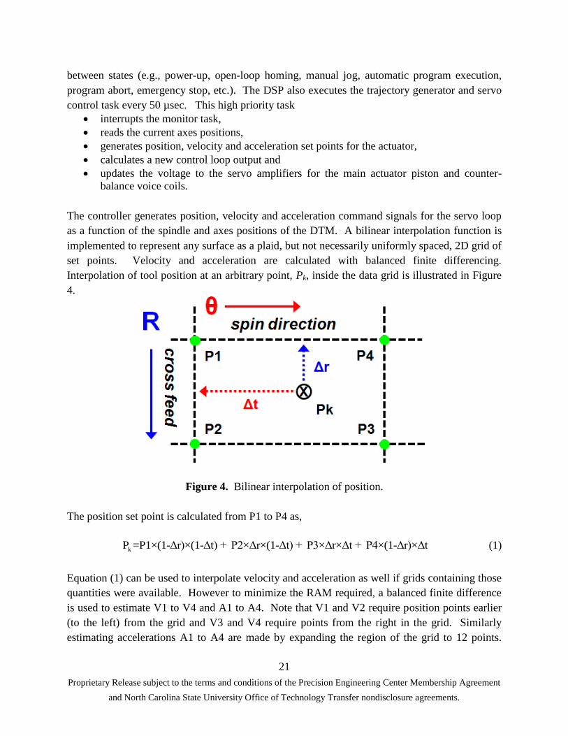
as a function of the spindle and axes positions of the DTM. A bilinear interpolation function is
implemented to represent any surface as a plaid, but not necessarily uniformly spaced, 2D grid of
set points. Velocity and acceleration are calculated with balanced finite differencing.
Interpolation of tool position at an arbitrary point, Pk, inside the data grid is illustrated in Figure
4.
Figure 4. Bilinear interpolation of position.
The position set point is calculated from P1 to P4 as,
kP =P1×(1-Δr)×(1-Δt) + P2×Δr×(1-Δt) + P3×Δr×Δt + P4×(1-Δr)×Δt (1)
Equation (1) can be used to interpolate velocity and acceleration as well if grids containing those
quantities were available. However to minimize the RAM required, a balanced finite difference
is used to estimate V1 to V4 and A1 to A4. Note that V1 and V2 require position points earlier
(to the left) from the grid and V3 and V4 require points from the right in the grid. Similarly
estimating accelerations A1 to A4 are made by expanding the region of the grid to 12 points.

22
Proprietary Release subject to the terms and conditions of the Precision Engineering Center Membership Agreement
and North Carolina State University Office of Technology Transfer nondisclosure agreements.
The final values for velocity and acceleration must be scaled according to the spindle speed and
cross feed velocity, which are continuously updated by the controller. Note that at each servo
update cycle the next point, Pk+1, is at most one grid position away from current location and the
intermediate results from the previous cycle can be used to reduce the computational load.
3.3 MACHINED OPTICAL SURFACES
3.3.1 FLAT BRASS TEST PART
A 12 mm OD flat brass sample was machined with the FLORA II holding position. The shape
of the machined surface is shown in Figure 5. With a spindle speed of 600 rpm, feed rate of 1
mm/min and tool nose radius of 2.393 mm, the theoretical finish is 0.04 nm. While the finish did
not achieve this value, it was equivalent to a fixed tool holder - 11 nm PV and 2 nm RMS.
Figure 5. 12 mm Brass flat with 11 nm PV figure error and 2 nm RMS surface finish
3.3.2 TILTED FLAT
To provide a test of the dynamic response of the FLORA II, a tilted flat was machined in brass.
For this test the surface shape in cylindrical coordinates is a linearly increasing cosine wave
described by Equation (2),
, cosr
z r AW
(2)
where A is the wave amplitude, W is the workpiece radius, r is the radial position of the tool and
θ is the spindle angle in radians. Because the contact angle between the tool and the workpiece
changes as a function of spindle rotation, a correction must be made for the tool nose radius, Tr,
as given by Equation (3).

23
Proprietary Release subject to the terms and conditions of the Precision Engineering Center Membership Agreement
and North Carolina State University Office of Technology Transfer nondisclosure agreements.
2
21 cos 1t r
Az T
W
(3)
This correction is a twice/revolution command with a magnitude on the order of 1 µm for the ±
500 µm range of motion for this particular tilted flat. The command calculated by the FLORA
II trajectory generator is thus the surface shape plus the tool radius correction (Equation (4)).
, ,p tz r z r z (4)
The FLORA II feedback controller with encoder position sensing and velocity and acceleration
feed-forward minimizes the following error. The velocity and acceleration for the tilted flat are
functions of the radial position, the spindle angle and the spindle rotation speed and are given by
Equations (4). A counterbalance system is used to reduce the influence of the FLORA II piston
inertia on the DTM axes. The feed-forward commands (acceleration and velocity) are also sent
to the open loop counterbalance pistons on the FLORA II (shown in the lower back in Figure 1).
The counterbalance system reduces the machine error motion at 10 Hz to a value less than 10
nm.
2
2
, sin
, cos
v
a
r dz r A
W dt
r dz r A
W dt
(5)
Figure 6. Less than 100 nm figure error was generated on a 50 mm diameter tilted flat brass
workpiece machined at 600 rpm with a PV tool motion of 1 mm.

24
Proprietary Release subject to the terms and conditions of the Precision Engineering Center Membership Agreement
and North Carolina State University Office of Technology Transfer nondisclosure agreements.
For the tilted flat, the position command as well as the velocity/acceleration feed-forward and
tool radius correction can be generated in real-time using Equations (5). For a more general
surface shape however, these need to be generated based on the desired shape which may come
from an optics design and may not have a specific equation.
The reason for machining a tilted flat was to demonstrate the capability of the actuator to follow
a 10 Hz sine wave with decreasing amplitude from OD to ID. Performance can be accessed by
interferometric measurement of the machined part using a flat reference mirror. The form error
shown in Figure 6 illustrates excellent fidelity in fabricating the tilted flat surface - the error is
less than 100 nm for a command range of 1,000,000 nm at 10 Hz.
Figure 7. Surface roughness measured at 4 points on the outside edge of the machined brass
tilted flat is less than 4 nm RMS. The main features are at the 3.3 µm/rev feed rate.
The surface finish using a long range fast tool servo generally degrades as the range of motion is
increased. For the FLORA II this does not appear to be the case for a stroke up to 1 mm and a
spindle speed of 600 rpm. The surface finish at 4 positions at the outside edge of the part is
shown in Figure 7; the high (upper left) and low (lower right) points of the tilted flat where the
velocity is zero as well as the points of maximum velocity (upper right and lower left) as the
servo passes through zero stroke. The cutting conditions for the finish pass were 600 rpm
spindle speed, 2 mm/min feed rate using a 2.393 mm radius tool and 1 µm depth of cut. The
surface finish for all positions is from 2-4 nm RMS, which is excellent.

25
Proprietary Release subject to the terms and conditions of the Precision Engineering Center Membership Agreement
and North Carolina State University Office of Technology Transfer nondisclosure agreements.
3.3.3 OFF-AXIS BICONIC REFLECTOR
The final optical surface in NASA’s Infrared Multi-Object Spectrometer [1] is a 96x96x25 mm
aluminum reflector which has a biconic shape. The aperture is decentered by (x0,y0)=
(-2.01,227) mm. The flat back surface is defined to be parallel to the mean normal vector from
the front surface, resulting in a tilt of 35.3° about the x axis. The aperture and optical axis are
shown in Figure 8.
Figure 8. Biconic reflector surface.
Figure 9. NRS component of biconic after removing the best fit sphere with radius 373 mm.

26
Proprietary Release subject to the terms and conditions of the Precision Engineering Center Membership Agreement
and North Carolina State University Office of Technology Transfer nondisclosure agreements.
A tool path for the biconic mirror was created by first removing the 35.3° tilt, translating the
lowest point (i.e., smallest z value) to the origin. Next the surface data points were interpolated
to a cylindrical mesh and tool radius compensation was performed. Finally, a least squares
sphere was fit to the resulting surface to reveal the NRS component as shown in Figure 9. The
range of FTS motion required is 288 µm. Within the defined clear aperture (shown as the mesh
patch) the FTS range is 128 µm.
Figure 10. The Biconic Reflector M4 mounted on the ASG 2500 DTM. FLORA II is shown on
right with the tool reflected in the mirror surface.
To test machining conditions, confirm tool
centering and eliminate all systematic errors
other than the fast tool servo, the best fit sphere
with was first machined into the substrate. The
figure error of this sphere was measured at 44
nm RMS and was considered satisfactory for
proceeding with the biconic surface. The
biconic mirror is shown in Figure 10
immediately after final machining with the
FLORA II FTS.
CGH Form Measurement
Form measurement of free-form surfaces can
be performed in a number of ways (e.g., Polaris
3D), but for this application a Computer
Figure 11. CGH fringe map showing the
measurement area and the alignment ring.

27
Proprietary Release subject to the terms and conditions of the Precision Engineering Center Membership Agreement
and North Carolina State University Office of Technology Transfer nondisclosure agreements.
Generated Hologram (CGH) was
used. The CGH includes
alignment fiducials to assure
correct placement of the hologram
in the interferometer. Initial
alignment for tip and tilt of the part
substrate and the CGH plane is
performed with a planar reference.
Then a spherical CGH is placed in
the converging beam of an F1.2
spherical reference. Lateral
alignment and focus of the CGH
mount is performed with this
specially made holographic optic.
The CGH alignment to the
interferometer is fine-tuned using
the spherical reference ring around
the part measurement area as shown in Figure 11. Since the CGH is actually a diffraction
grating, a 2 mm pupil is then placed at the focus and used to mask all but the first diffraction
order. Finally, the part is aligned to the CGH in six degrees of freedom. This is an iterative
process until a minimum error is found.
Results
The surface finish measured with a Zygo NewView 5000 SWLI was 3 nm RMS. RMS figure
error was 127 nm and is dominated by astigmatism. The shape of the astigmatism is very similar
to that of the FTS excursion shown in Figure 9. Applying a gain to the FTS motion of 1.005
removes the astigmatism and reduces the RMS figure error to 43 nm as shown in Figure 12. The
gain change was performed in Matlab after importing the MetroPro measurement data file.
3.4 CONCLUSIONS
The FLORA II actuator has been fully integrated into the ASG 2500 DTM and used to machine
non-rotationally symmetric surfaces with excellent surface finish and form fidelity. A graphical
interface has been programmed that is user friendly and comprehensive – supporting all aspects
of machine setup and operation. A data format and an interpolation code have been implemented
for arbitrary surfaces of the form, Z = F(r,θ) and Matlab code for creating a FLORA input file
has been developed.
Figure 12. CGH measurement with astigmatism removed
by increasing the FTS gain. Residual RMS error is 43 nm.

28
Proprietary Release subject to the terms and conditions of the Precision Engineering Center Membership Agreement
and North Carolina State University Office of Technology Transfer nondisclosure agreements.
REFERENCES
[1] Garrard K, Sohn A, Ohl R, Mink R, Chambers V. Off-Axis Biconic Mirror Fabrication.
Proc. of the 3rd
International Meeting of EUSPEN. 2002; 277-280.

29
Proprietary Release subject to the terms and conditions of the Precision Engineering Center Membership Agreement
and North Carolina State University Office of Technology Transfer nondisclosure agreements.
4 INTEGRATED PRESCAN OPTICS
FOR LASER PRINTERS
Alex Sohn
Research Assistant
Kenneth P. Garrard
Senior Research Associate
Precision Engineering Center
The design of a two element reflective optical system for a laser prescan unit has been
completed. The optical system has been machined from a single piece eliminating the need for
assembly and alignment of the two mirrors. However the mirrors in their correct orientation in
the optical system are not rotationally symmetric about any axis. Matlab software has been
developed to decompose a multi-element optical system into a best fit asphere and a non-
rotationally symmetric surface. Tool path data for fabrication on the ASG 2500 Diamond
Turning Machine augmented with a FLORA II fast tool servo are automatically generated by this
software.
30
Proprietary Release subject to the terms and conditions of the Precision Engineering Center Membership Agreement
and North Carolina State University Office of Technology Transfer nondisclosure agreements.
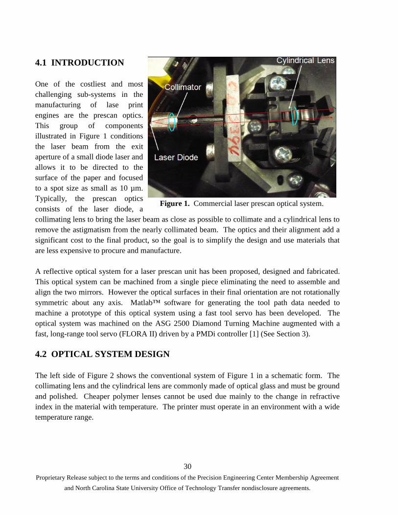
Figure 1. Commercial laser prescan optical system.
4.1 INTRODUCTION
One of the costliest and most
challenging sub-systems in the
manufacturing of lase print
engines are the prescan optics.
This group of components
illustrated in Figure 1 conditions
the laser beam from the exit
aperture of a small diode laser and
allows it to be directed to the
surface of the paper and focused
to a spot size as small as 10 µm.
Typically, the prescan optics
consists of the laser diode, a
collimating lens to bring the laser beam as close as possible to collimate and a cylindrical lens to
remove the astigmatism from the nearly collimated beam. The optics and their alignment add a
significant cost to the final product, so the goal is to simplify the design and use materials that
are less expensive to procure and manufacture.
A reflective optical system for a laser prescan unit has been proposed, designed and fabricated.
This optical system can be machined from a single piece eliminating the need to assemble and
align the two mirrors. However the optical surfaces in their final orientation are not rotationally
symmetric about any axis. Matlab™ software for generating the tool path data needed to
machine a prototype of this optical system using a fast tool servo has been developed. The
optical system was machined on the ASG 2500 Diamond Turning Machine augmented with a
fast, long-range tool servo (FLORA II) driven by a PMDi controller [1] (See Section 3).
4.2 OPTICAL SYSTEM DESIGN
The left side of Figure 2 shows the conventional system of Figure 1 in a schematic form. The
collimating lens and the cylindrical lens are commonly made of optical glass and must be ground
and polished. Cheaper polymer lenses cannot be used due mainly to the change in refractive
index in the material with temperature. The printer must operate in an environment with a wide
temperature range.

31
Proprietary Release subject to the terms and conditions of the Precision Engineering Center Membership Agreement
and North Carolina State University Office of Technology Transfer nondisclosure agreements.
Figure 2. Conventional prescan lens design (left) and new 2-mirror reflective system (right).
If the lenses shown in Figure 2 are replaced with reflective optics, the refractive index of the
material becomes irrelevant. Thus, molding polymer reflectors becomes a distinct possibility.
One possible layout for such a design using reflective optics is shown at the right in Figure 2.
The primary mirror is an ellipsoid and it removes most of the divergence from the beam while
the secondary mirror removes whatever divergence remains as well as the aberrations due both to
laser diode astigmatism and the off-axis placement of the primary mirror. Thus, the secondary
mirror is biconic.
As a prototype, both mirrors were machined into the end of a small cylinder using the FLORA II
fast too servo. As shown in Figure 3, the mirrors have a substantially larger radius than the
radius of rotation and appear almost as two flat surfaces in a spherical parent surface. The cross
section in Figure 3 shows the spacing of the mirrors and the laser source.
Figure 3. Solid model of mirror surfaces and beam path and a cross section of the system.

32
Proprietary Release subject to the terms and conditions of the Precision Engineering Center Membership Agreement
and North Carolina State University Office of Technology Transfer nondisclosure agreements.
Figure 4. Machining layout.
4.3 FABRICATION
Both optical surfaces can be machined in a single
setup on a metal substrate guaranteeing the
alignment of the two mirrors. As shown in Figure
4, the volume of material to be removed is quite
small and the prototype can be fabricated without
rough machining a spherical pocket or slot prior to
performing the final machining operation. The
diamond tool must be selected to reach into the
pocket and machine the symmetric surface without
touching the clearance face of the tool.
4.3.1 GEOMETRIC ANALYSIS
Each mirror can be defined as a general biconic in Cartesian coordinates with Equation (1),
2 2
0 0
2 22 2
0 0
,1 1 1 1
XZ YZ
XZ XZ YZ YZ
c x x c y yZ x y
k x x c k y y c
(1)
where the origin is (x0,y0,0), cXZ is the curvature in the XZ plane, cYZ is the curvature in the YZ
plane and kXZ and kYZ are the conic constants in the two orthogonal planes. The prototype design
parameters are given in Table 1 and the apertures and their orientation with respect to each other
are defined in Table 2.
Table 1. Surface parameters for prescan optics.
Plane Curvature (1/mm) Conic constant
M1 XZ 1/30 1
YZ 1/30 1
M2 XZ 1/13.905686 -2.396222
YZ 1/34.682089 -60.00092
Table 2. Aperture definition of prescan optics.
Aperture (mm) Translation (mm) Tilt (radians)
radius x decenter y decenter x y z x y z
M1 0.572995 0 0 0 2 0 pi/4 0 0
M2 0.916568 0 0 0 -2 0 -pi/4 0 0

33
Proprietary Release subject to the terms and conditions of the Precision Engineering Center Membership Agreement
and North Carolina State University Office of Technology Transfer nondisclosure agreements.
Both surfaces are on-axis (i.e., no decenter) and M1 is an oblate ellipsoid of revolution while M2
is a non-rotationally symmetric surface of two very different hyperboloids. These two mirrors are
shown in Figure 5. They have been translated to the correct separation but not tilted. Figure 6
shows M1 and M2 after tilting the mirrors along with a wireframe plot of an annular segment of
the best fit sphere whose center is constrained to lie on the z axis (i.e., the axis of rotation during
machining). The chief ray at the center of each aperture is shown as a dotted line and the center
of the best fit sphere is shown as a dot. For this optical system a conical base surface provides a
better fit, that is, the residuals have a smaller magnitude and the FTS excursion is reduced.
(a) (b)
Figure 5. (a) The input mirror (M1) and the output mirror (M2) are shown as defined by
Equation 1 and Table 1. (b) The laser prescan optical system with the mirrors in the correct
orientation as defined by Table 2.
4.3.2 TOOLPATH GENERATION
The ASG 2500 diamond turning machine can be programmed to produce the spherical surface
shown in Figure 7 while the FTS moves the tool in the sagittal direction as a function of the
spindle rotation angle and the cross-feed axis position. The FTS motion plus the underlying
sphere form the desired mirror surfaces. The mirror curvatures are much smaller than that of the
best-fit sphere (i.e., they are "flatter" than the sphere), thus the shape of the FTS motion within
the mirror apertures will be convex. The range of servo motion required is 297 µm.

34
Proprietary Release subject to the terms and conditions of the Precision Engineering Center Membership Agreement
and North Carolina State University Office of Technology Transfer nondisclosure agreements.
Surface finish and form fidelity are likely to be improved if the range of FTS excursion is
minimized. This can be done by machining an aspheric surface with the DTM. Compensation
for the contact point along the radius of the tool must be included. This compensation is done
along meridians from the axis of rotation to the edge of the workpiece. An asphere is then
subtracted from the result to form a 2D lookup table of FTS positions as a function of radial and
angular position. A part program for the ASG 2500 is created to machine the aspheric shape,
which in this case is a 43.87° cone. A Matlab script has been developed to generate a lookup
table for the FLORA II controller and the dSPACE Variform FTS controllers as well as the
aspheric motion program for any two surface biconic optical system. This design file needed by
the Polaris3D spherical profilometer [2] to measure the resulting part is also created. The steps
in this algorithm are as follows:
1. Generate a circular aperture grid for each mirror, M1 and M2.
2. Calculate z positions for each (x, y) point within the apertures.
3. Translate and rotate the mirror surface data sets to their positions in the optical system.
4. Create a cylindrical coordinate grid for the optical system whose center is on the axis of
rotation of the DTM spindle.
5. Find all data points on the cylindrical grid in the tilted elliptical apertures of M1 and M2.
6. Interpolate mirror surface data to the cylindrical coordinate aperture grid.
7. Extend the aperture masks to equal radii and uniform angles.
8. Perform tool radius compensation along each meridian in each aperture.
9. Interpolate compensated points onto a common radial grid.
10. Find the mid-range sagittal value at each radius.
11. Fit a radial polynomial to the mid-range data.
12. Form a table of residuals. This is the FTS excursion.
13. Create a motion program following the cross-section of the aspheric surface.
14. Output the FTS excursion formatted for the FLORA II controller.
15. Output a "design file" for the Polaris3D spherical measuring machine.
The aperture masks for M1 and M2 in the cylindrical coordinates of the optical system are
ellipses. But the FTS control system requires a matrix of data to describe the motion of the tool.
Each row contains height data at a radius and each column is at an angle. The rows and columns
need not be equally spaced, but the matrix must be plaid; that is, all rows (radii) have a data point
for each column (angle). Thus Step (7) extends the elliptical apertures to angular segments,
shown as the boundaries of the wireframe surfaces in Figure 6. The pole represents the spindle
axis for turning the optical system and the two shaded patches are the M1 and M2 mirror
surfaces. The origin of the cylindrical coordinate system is (θ=0, r=0); however this is not
necessarily the optimal location for the axis of rotation. The (x, y) center of a least squares
sphere fit to the system data for the prescan optics has an origin 17 µm from (0,0). In this case,

35
Proprietary Release subject to the terms and conditions of the Precision Engineering Center Membership Agreement
and North Carolina State University Office of Technology Transfer nondisclosure agreements.
Figure 6. Optical system with tool Figure 7. FTS motion for monolithic
radius compensation. prescan optics machining.
Figure 8. Combined optical system tool path.
the FTS excursion is reduced by only a few micrometers by including this additional translation
of the mirrors. To reduce the complexity of the system analysis and machining setup the origin
was fixed at (0,0). In Step (11), the best fit asphere was found to be very close to conical for this
optical system. Figure 7 also shows the effect of tool radius compensation along each meridian
on the cylindrical aperture grid. The wire frame overlay gives at the position of the tool center
when machining each mirror.
Subtracting the best fit asphere from the
radius compensated tool positions
shown in Figure 6 gives a table of FTS
positions for machining the optical
system. These positions are on a fine
cylindrical grid with a maximum
spacing of 16 µm between grid points.
Figure 7 shows the complete FTS tool
path within the radial aperture of the
mirrors. The required tool excursion is
220 µm. The tool positions are extended
10° to either side of each aperture so that
the FTS doesn't abruptly change
direction at the edge of the desired clear aperture. The space between the mirrors in the
azimuthal direction is a linearly interpolated surface that is added to the asphere swept out by the
DTM axes.

36
Proprietary Release subject to the terms and conditions of the Precision Engineering Center Membership Agreement
and North Carolina State University Office of Technology Transfer nondisclosure agreements.
The FTS tool motion and the best fit asphere can be added to create the surface shown in Figure
8. This annular surface describes the location of the tool center when machining the prescan
optical system.
4.4 RESULTS
The prescan optical system was machined using the FLORA II actuator mounted on the ASG
2500 DTM (see Figure 9). The FLORA II control system was programmed to perform bilinear
interpolation over the cylindrical grid of sag values for the excursion shown in Figure 7. The
controller positions the tool servo and two counter-balance masses using feedback and
feedforward control and thus needs commanded position, velocity and acceleration. The
interpolation grid was evenly spaced radii from 1.27 mm to 2.6 mm in increments of 16 µm. The
angular spacing was uniform within the mirror apertures at 0.13°, which gives a maximum arc
length of 6 µm between points. For this optical system, the best fit polynomial order was set to
1, so the aspheric surface swept out by the DTM was a cone. The cone angle is nearly 45°. The
finish pass was cut at 80 rpm with a cross feed of 0.16 mm/min, yielding a feed of 2 µm per
revolution. The tool radius was 82.7 µm.
Figure 9. FLORA II machining prescan mirrors (left) and finished part (right).
Interestingly, the surface finish measurement shown in Figure 10 of the M2 mirror shows a
repeating pattern at 35 µm which may be print-through from rough machining. While the
surface finish is not stunning, 8 nm Ra is quite good considering the high accelerations of the
servo at the aperture edges.

37
Proprietary Release subject to the terms and conditions of the Precision Engineering Center Membership Agreement
and North Carolina State University Office of Technology Transfer nondisclosure agreements.
Figure 10. Surface finish measurement with Zygo NewView 5000 of the M2 biconic mirror.
The concave surface shown in Figure 9 was measured on Polaris3D (see Section 1) by parking
the rotary table (θ) at +30°, spinning the part at 20 rpms and translating the Z axis (and the part)
away from probe. With tracking engaged, the controller moves the R axis to keep the probe
focused on the part. This setup allowed the probe to see the flat at the bottom of the part, the
conical mirror surfaces and a portion of the upper rough machined flat. The diamond turned
center flat is useful for alignment of the optic and to remove tilt before comparing the
measurement data with the intended surface shape.
(a) (b)
Figure 11. Form measurement of the optical system with Polaris3D. The raw measurement data
is shown in (a) and the data after removal of the cone machined by the ASG 2500.
Figure 11 shows the measurement results. Figure 12(a) is a plot of the raw measurement data for
the optical system. The 43.87° base cone was subtracted in Figure 8(b) indicating the tool
motion away from the cone (toward the center of the part) needed to create the nearly flat mirror

38
Proprietary Release subject to the terms and conditions of the Precision Engineering Center Membership Agreement
and North Carolina State University Office of Technology Transfer nondisclosure agreements.
surfaces. Figure 12 is a top down view of the error when the measurement is subtracted from the
shape of the optical design shown in Figure 5(b). The result is an RMS error of 730 nm with the
error largest on the outside and smallest on the inside. The result is a tilt angle that is 5
milliradians more than desired.
Figure 12. Optical system surface error in the mirror apertures.
4.5 CONCLUSIONS
The design and fabrication for a reflective prescan laser optical system has been completed.
Tool path generation for an arbitrary biconic two mirror system has been coded in Matlab. The
data tables needed to machine the mirrors with the FLORA II FTS control system are generated
by this Matlab code. In addition, a motion program is output describing the best-fit rotationally
symmetric asphere that is machined simultaneously by the ASG 2500 Diamond Turning
machine. The optical system was machined and measured with Polaris 3D. The significance of
the residual tilt angle error on the optical performance of the system has not been evaluated.
REFERENCES
1. Zdanowicz, E., Design of a Fast Long Range Actuator -- FLORA II. Master's Thesis, North
Carolina State University, 2009.
2. Garrard, K. Polaris 3D Operation and Control. Precision Engineering Center Annual Report,
27, 27-46, North Carolina State University (2009).

39
Proprietary Release subject to the terms and conditions of the Precision Engineering Center Membership Agreement
and North Carolina State University Office of Technology Transfer nondisclosure agreements.
5 FABRICATION AND TESTING OF AN AIR AMPLIFIER
AS A FOCUSING DEVICE FOR ELECTROSPRAY
IONIZATION MASS SPECTROMETRY
Guillaume Robichaud
Graduate Student
Thomas Dow
Dean F. Duncan Distinguished Professor
Department of Mechanical and Aerospace Engineering
Alex Sohn
Precision Engineering Center Staff
Mass spectrometry is an analytical method used to identify molecule and complex protein based
on the ration of their mass and the number of charge they carry when measured. Application
and use of mass spectrometry has been growing extremely fast during the last decade. It is
currently extensively used in analytical chemistry, cancer research, drug testing, explosive
detection, etc. To be measured, molecules first have to be transferred into gas phase and
ionized. A technique of obtaining gas phase ion that has revolutionized mass spectrometry is
called electrospray ionization, where gas phase ions are extracted from a solution flowing in a
thin capillary using a powerful electrical field. However, it is estimated that less than 1% of ions
generated by an electrospray ionization source will be sampled by the mass spectrometer. This
is mainly due to the low transfer efficiency of ions between electrospray source and the
instrument inlet. Through the joint effort of precision engineering and computational fluid
dynamics, an aerodynamic ion focusing device has been designed and fabricated using a single
point diamond turning machine. Several tests have been performed to evaluate the performances
of the device.

40
Proprietary Release subject to the terms and conditions of the Precision Engineering Center Membership Agreement
and North Carolina State University Office of Technology Transfer nondisclosure agreements.
5.1 INTRODUCTION
Mass spectrometry is an analytical technique widely used in biochemistry to characterize and
identify molecules and proteins. It is a fast growing science and plays a critical role in cancer
and proteomic research. Modern mass spectrometers use electric or magnetic fields to
differentiate gas phase molecules according to the relation between their mass and charge (m/z)1.
The molecules of interest (analyte) are often in solution and therefore need to be transferred to
gas phase and charged prior to be captured by the mass spectrometer. One of the preferred
methods is the electrospray ionization technique (ESI) [1]. ESI-MS was developed by
Yamashita and Fenn at Yale in 1984 [2] and allows a wide range of molecule size to be
transferred directly to gas phase in line with the spectrometer. ESI is that it is a very soft
ionization technique, meaning that energy added to the molecule is relatively low, allowing large
molecules such as proteins to be transferred into gas phase without fragmenting. ESI-MS
consists of a small capillary tube through which flows an analyte diluted in a buffer solution
containing solvent and a small percentage of formic acid (charges). The intake needle of the
mass spectrometer is positioned a few millimeters from the capillary exit and an electrical
potential between the capillary and the mass spectrometer needle is applied as shown in Figure 1.
The resulting electrical field will cause a thin jet of highly charged solution to be ejected from
the ESI tip, from which gas phase ions will eventually arise as solvent evaporates. Creation of
singular ions during electrospray depends upon a complex interaction between the size of the
analyte molecule, the flow rate, the nature of the solvent, the intensity of the electrical field, the
concentration of the analyte in the solvent and the temperature. However, the efficiency of the
ESI-MS does not only depend on the ability to create gas-ions from liquid analyte but also
greatly depends on the efficiency of the transmission of these ions to the mass spectrometer. It is
estimated that less than 1% of the ions produced will be sampled by the mass spectrometer.
Most of the loss is encountered during the transfer between the ESI capillary and the MS inlet, as
ions of same polarity will be scattered by repulsive Coulombic force before they can reach the
inlet of the mass spectrometer.
1 The dimensionless mass-to-charge ratio (m/z) is used to characterize the mass spectrum, where m is the unified
atomic mass (in Dalton) and z is the number of elementary charges.

41
Proprietary Release subject to the terms and conditions of the Precision Engineering Center Membership Agreement
and North Carolina State University Office of Technology Transfer nondisclosure agreements.
Efficiency of ESI-MS is critical because the size of the sample to be analyzed in applications
such as medical research or forensics can be limited. Improving the efficiency or the sensitivity
of the ESI-MS would lower the detection limit or the minimum sample size needed. This
section addresses the design, fabrication and testing of a precision engineered air amplifier to
aerodynamically focus the scattering ions toward the mass spectrometer inlet to increase the
number of ions captured. It involved faculty and staff in mechanical engineering studying fluid
flow and design/fabrication as well as faculty and staff in chemistry to study the efficiency in MS
experiments.
5.2 THE AIR AMPLIFIER
Proof of concept showing signal improvement using an air amplifier has been made using a
crude commercial device [3-6]. It was found that imprecise gap control and misalignment were
impacting the performance and repeatability of the results. The Computational Fluid Dynamics
Lab worked together with the Precision Engineering Center to develop an aerodynamic profile
that provided suitable fluid flow and was suitable for fabrication. The first calculations of the
gas dynamics of the flow within the air amplifier devices has been performed using an in-house
computational fluid dynamics code called REACTMB. The air amplifier uses the Coanda effect2
in order to create a low pressure zone that enables air entrainment into the air nozzle and
eventually focus the ions that are generated by electrospray ionization into the mass
2 Tendency of a fluid to stay attached to an adjacent curved surface
2-4 kV
30-40V
ESI Capillary
(ID : 15-30 µm)
MS Inlet
(ID : 500 µm)
Desolvating ions
Gas phase ions
Cluster of ions
and solvent
Focusing effect of
flow caused by the
air amplifier
Figure 1. Electrospray Ionization with Air Amplifier

42
Proprietary Release subject to the terms and conditions of the Precision Engineering Center Membership Agreement
and North Carolina State University Office of Technology Transfer nondisclosure agreements.
spectrometer, increasing the sensitivity of the instrument. Images from CFD model (Figure 2)
shows the velocity profile of the pressurized N2 curved by the Coanda effect (left) as well as the
focusing effect on the electrosprayed ions (right).
Figure 2. Aerodynamic model of the air amplifier (Left: Coanda profile. Right: Stream lines.)
5.2.1 1ST
ITERATION OF AIR AMPLIFIER
According to the CFD model, the ideal annular gap was in the range of 50-70 µm and to ensure a
uniform and radially symmetrical flow, the annular gap faces had to be parallel to < 1 µm. In
addition, the surface finish of the Coanda surfaces had to be smooth and radially symmetric.
Because the optimal annular gap was to be set experimentally, the first iteration of the air
amplifier had an annular gap that can be modulated from 50 µm to 70 µm with three
piezoelectric actuators illustrated in Figure 3.
Figure 3. Section view of the 1
st iteration of the air amplifier.

43
Proprietary Release subject to the terms and conditions of the Precision Engineering Center Membership Agreement
and North Carolina State University Office of Technology Transfer nondisclosure agreements.
When high pressure air is introduced to the gas plenum, the air amplifier created a Venturi effect
and static pressure has been measured along the flow axis for different pressure and annular gap
position using a pitot tube. The minimum static pressure was measured 1 mm downstream of the
annular gap, revealing the existence and location of a focal point. Moreover, increasing the
annular gap width had the same effect on the flow profile as increasing the plenum pressure.
Several mass spectrometry experiments were performed to evaluate the effect of the air amplifier
on the signal abundance. On a mass spectrum, signal abundance is reported for each m/z value
and is proportional to the number of ion detected for that range. Signal abundance is often
reported in term of the relative abundance or the percentage of the most abundant ion. Absolute
abundance is dimensionless and depends on parameters specific to the instrument. Absolute
abundance is a valid figure of merit to compare sets of measurements taken on the same
instrument under different operating conditions – such as with and without the air amplifier. To
systematically explore the experimental space defined by the many variables that can affect the
performance of the air amplifier (position, plenum pressure, annular gap width, solvent
composition, ESI voltage, etc), fractional factorial design was used to find the significance of
each. The results showed that signal improvement could not be obtained under all condition but
were significant at higher solvent flow rates and larger ESI capillary tips (up to 34 folds of
improvement in this case [7]).
5.2.2 2ND
ITERATION DESIGN AND FABRICATION
Based on the results of the first design, a second design of the air amplifier has been fabricated.
The objectives were to reduce the cost and to make the device more compact; that is, to reduce as
the length of the mass spectrometer inlet tube (see Figure 4). A longer capillary tube decreases
significantly the efficiency of the ion transfer in the mass spectrometer as the opportunity for
ions to collide and neutralize with the capillary increases. As desolvation of ions in gas phase
typically continues in the MS inlet tube (typically kept at 200-250 ºC), another hypothesis
suggest that the cooling of the ions in the extended capillary tube could slow down the
desolvation process and therefore reduce the number of gas phase. Also, a less expensive and
more compact air amplifier is now possible since it was demonstrated that the piezoelectric
actuators are not necessary.

44
Proprietary Release subject to the terms and conditions of the Precision Engineering Center Membership Agreement
and North Carolina State University Office of Technology Transfer nondisclosure agreements.
Figure 4. Reduction of MS inlet tube length
As in the first design, the CFD model was used to test different aerodynamic profiles and
different configurations. Since there was no indication that a change in the Coanda profile would
result in significant signal improvement, aerodynamic outline of the Coanda profile and annular
gap remained unchanged. Only the length of the inlet and outlet cones would change to allow a
shorter MS inlet tube. A CFD model was also used to verify the effect of these changes in
geometry on the signal and also how close the air amplifier could be positioned with respect to
the MS inlet before starting to obstruct the flow. With the new design, it will now be possible to
reduce the MS tube length by up to 80% (134 mm to 23 mm). Also, new design only has one
insert, such that the outlet cone is now machined directly in the base plate. Not only does this
also allow a shorter outlet cone,, but it also eliminates the risk associated with the misalignment
of that insert. To keep the plenum size the same, the upstream cone length had to be extended.
Observation of pitot tube measurement performed on the first iteration indicated that the length
of the upstream (intake) cone had little influence on the air flow profile. This hypothesis was
also confirmed by the CFD model. Extensive work has been made by the AECFD laboratory to
include the charged particles in the model so that ion abundance can be predicted. The model
did not predict a significant drop in abundance due to the shorter outlet cone. However, the
charged particle model had not been fully validated at this time so it was decided to fabricate an
air amplifier that had removable outlet cone sections so that effect of cone length can be
determined experimentally.
MS inlet has been
reduced

45
Proprietary Release subject to the terms and conditions of the Precision Engineering Center Membership Agreement
and North Carolina State University Office of Technology Transfer nondisclosure agreements.
Figure 5. Simulation used to design custom made diamond tool and determine tool setup
In the second iteration of the air amplifier the Coanda radius is machined directly in the base of
the device as shown in Figure 5. As access to this radius is limited, a custom diamond tool had
to be designed and machining simulation had to be performed using Solidworks® to ensure that
there would not be any interference between the tool holder and the part during machining of the
Coanda radius. Also shown on this figure, the tool was required to have a small included angle
and a large sweep angle to be able to machine the entire radius (90°) and also reach the back of
the bore. The clearance under the tool tip also had to clear the lower part of the tool while
machining the 5.15 mm OD. Additional lapping was required to create a relief angle under the
tool to ensure that this clearance was achieved. In the first iteration, because of the presence of
the piezoelectric actuators that had to be installed and shimmed, the final height of the insert that
set the annular gap had to be measured using a coordinate measurement machine (CMM). In this
case, the tool position given by the axis encoder of the diamond turning machine has been used
to measure precisely the part heights and set the annular gap to 50 µm.
5.2.3 SECOND ITERATION TESTS
Static pressure measurements for the second iteration of air amplifier were performed using a
compound pressure transducer with a range of ±5 psig (±5 V) together with a LVDT for position
measurement. With this setup it was possible to measure with greater resolution and accuracy
the static pressure as a function of the position in the air amplifier. In a first series of
measurements, the static pressure profile was measured for different cone lengths. Results are
presented in Figure 6. First, it can be observed that the location of the focal point remains
relatively unchanged (1-2 mm downstream of the annular gap) for different cone lengths. It can
also be observed that the minimum pressure (maximum vacuum) decrease significantly as the
cone length decreases. This phenomenon limiting the minimum cone length had been predicted
by the CFD models. It is caused by recirculation of air that creates back pressure interfering with
the flow in the air amplifier. This back pressure can be seen clearly in figure for the
measurements performed with cone length of 11.85 mm and 17.85 mm.
30° Included Angle
200 µm Tip Radius
150° Sweep
12° Primary conical Clearance Angle
35° Relief Angle Under Tool Tip
5.15 mm
35°

46
Proprietary Release subject to the terms and conditions of the Precision Engineering Center Membership Agreement
and North Carolina State University Office of Technology Transfer nondisclosure agreements.
Figure 6. Static Pressure Measurement for 2nd iteration of air amplifier
One of the major issues with the commercial air amplifier that was used in previous experiments
was the lack of radial symmetry of the air flow caused by its threaded annular gap adjustment
that offered limited annular gap width control and poor parallelism. A non-radially symmetric
air flow affects the capability of obtaining a precise and consistent aerodynamic focal point. To
measure the symmetry of the flow, stagnation pressure has been measured at 1 mm from the
outlet of the air amplifiers along the vertical and horizontal axis. These measurements have been
performed on both the new precision engineered air amplifier and the threaded commercial
version. 3D plots of the stagnation pressure as a function of the radial position are presented in
Figure 7, where 0 mm is the central axis of the air amplifier. A significant improvement in radial
symmetry can be observed.

47
Proprietary Release subject to the terms and conditions of the Precision Engineering Center Membership Agreement
and North Carolina State University Office of Technology Transfer nondisclosure agreements.
Figure 7. Stagnation pressure measured 1 mm from commercial air amplifier outlet.
5.2.4 LTQ-FTMS TESTS
The LTQ-FTMS used for this series of experiment is a tandem mass spectrometer, meaning that
it actually consist of two mass spectrometers in series. Only the front LTQ mass spectrometer
was used for these experiments to minimize the possible signal loss caused by the internal ion
transport. As mentioned earlier, one of the principal motivations for designing a second iteration
of the air amplifier was to reduce the length of the MS inlet tube. A first experiment was
performed to quantify the signal loss due to the extended capillary alone. To do so, signal was
collected with both the regular 3 mm MS inlet and the extended 43 mm inlet (no air amplifier)
under the same conditions. Ion abundance decreased by about 3 folds when using the extended
MS inlet of 43 mm is used.
The 43 mm MS inlet length is only necessary if all air amplifier cone lengths are used. If cone
extension lengths are removed, the MS inlet extended length can be reduced to 23 mm. It was
already shown in previous section that outlet cone length had a significant impact on the flow
inside the air amplifier.
To quantify the effect of the air amplifier on the ion abundance, measurements were performed
under the exact same conditions, varying only the cone length of the air amplifier. As it can be
seen in Figure 8, reducing the air amplifier cone length does not reduce the air amplifier signal.
For that reason, the remaining of the experiments will be performed without the cone length
extension (total cone length of 11.85 mm) and the mass spectrometer inlet extension of 23 mm.
Commercial Air Amplifier
Precision Engineered
Air Amplifier

48
Proprietary Release subject to the terms and conditions of the Precision Engineering Center Membership Agreement
and North Carolina State University Office of Technology Transfer nondisclosure agreements.
0
10
20
30
40
50
60
70
29.85 mm 23.85 mm 17.85 mm 11.85 mm
Ion
Inje
ctio
n T
ime
(m
s)
Ion Injection Time
Median
Figure 8. Ion injection time as a function of air amplifier cone length
As mentioned earlier, one of the hypotheses to explain signal loss due to an extended capillary
was the impact that the non heated capillary could have on the desolvation of the analyte. In
order to test this hypothesis, a wire element was used to generate additional heat to the extended
capillary as shown in Figure 9.
Figure 9. Experimental setup to heat MS inlet capillary
Several experiments have been performed with different heat inputs and results showed that no
additional improvement could be obtained by heating up the capillary as shown in Figure 10.
Results actually showed a slight loss in signal when additional heat was applied. If analyte is
already completely dissolved, providing additional heat energy to the molecule will cause
A
Adjustable DC
source
Nichrome 60, 32 AWG
wound in parallel to
avoid creating magnetic
field
Polyimide film
160 °C Measured at tip with
thermocouple probe with 0.6
Amp DC, same as temperature
measured on tip of regular MS
inlet
PTFE Shrink
tube
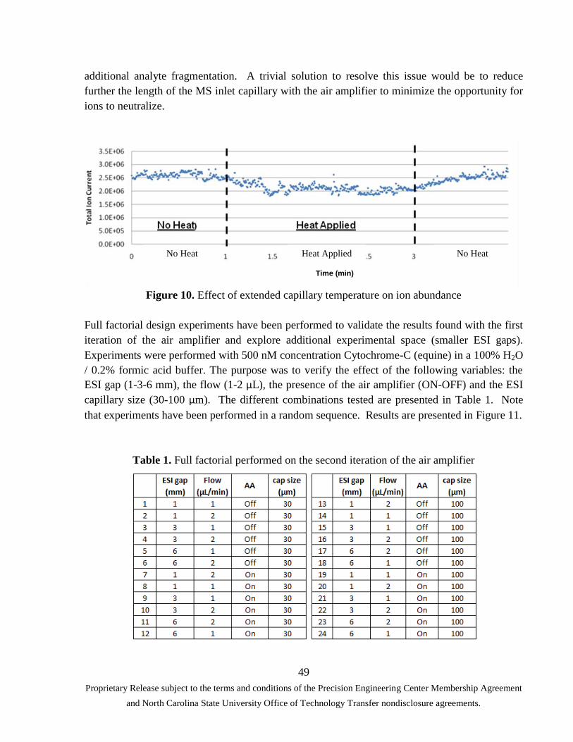
49
Proprietary Release subject to the terms and conditions of the Precision Engineering Center Membership Agreement
and North Carolina State University Office of Technology Transfer nondisclosure agreements.
additional analyte fragmentation. A trivial solution to resolve this issue would be to reduce
further the length of the MS inlet capillary with the air amplifier to minimize the opportunity for
ions to neutralize.
Figure 10. Effect of extended capillary temperature on ion abundance
Full factorial design experiments have been performed to validate the results found with the first
iteration of the air amplifier and explore additional experimental space (smaller ESI gaps).
Experiments were performed with 500 nM concentration Cytochrome-C (equine) in a 100% H2O
/ 0.2% formic acid buffer. The purpose was to verify the effect of the following variables: the
ESI gap (1-3-6 mm), the flow (1-2 µL), the presence of the air amplifier (ON-OFF) and the ESI
capillary size (30-100 µm). The different combinations tested are presented in Table 1. Note
that experiments have been performed in a random sequence. Results are presented in Figure 11.
Table 1. Full factorial performed on the second iteration of the air amplifier
No Heat
Heat Applied
No Heat
Time (min)

50
Proprietary Release subject to the terms and conditions of the Precision Engineering Center Membership Agreement
and North Carolina State University Office of Technology Transfer nondisclosure agreements.
Figure 11. Full Factorial Design experiment results (sum of 19
+, 9
+ and 8
+ of Cyt-C)
Those results are in accordance with what was discovered with the first iteration of the air
amplifier, i.e. that very little improvement was obtained with 30 µm ID ESI capillary. On the
other hand significant improvement is also obtained at 100 µm ID ESI capillary, where no signal
can be obtained without the air amplifier. This signal improvement at larger tip opens the door
to electrospray at higher flow as maximum flow in a 30 µm capillary is 3 µL/min and flow as
high as 10 µL/min are possible with the 100 µm capillary tip. However, the greater is the flow
rate, the larger is the radius (r) of initial droplets formed during electrospray as showed by the
following equation (1) where is the fluid density, Q is the flow rate and γ the surface tension of
the fluid.
1
2 3r Q (1)
This increase in initial droplet size signifies that more desolvation is necessary for the droplet to
release their gas phase ions. Therefore, even if an increase in flow means that more analyte is
electrosprayed for every unit time, it will not necessarily translate into a stronger signal if the
desolvation is not complete. To further explore this experimental space and show the effect of
air amplifier on desolvation, ion abundance as a function of flow rate was measured at 2 different
ESI distance (3 mm and 6 mm). As seen in Figure 12, an increase in flow rate at 3 mm does not
translate into an increase in abundance. On the other hand, results at 6 mm ESI gap show that
total ion current still increase linearly with flow rates up to 9 µL/min (maximum stable flow
obtained with 100 µm tips). We expect signal to be lower as ESI distance increases, however
increase in desolvation at larger ESI distance assisted by the air amplifier eventually compensate
for the losses resulting from the greater ESI distance. These results confirm the effect of the air
amplifier on the desolvation of the ions.

51
Proprietary Release subject to the terms and conditions of the Precision Engineering Center Membership Agreement
and North Carolina State University Office of Technology Transfer nondisclosure agreements.
Figure 12. Total Ion Current as a function of flow rate at 3 mm ESI gap
5.3 CONCLUSIONS
A new iteration of the air amplifier has been designed and fabricated with a fixed annular gap of
50 µm and a shorter outlet cone to reduce signal losses caused by the extended capillary. Using
fractional factorial design, variable having an impact on the performance of the air amplifier
have been identified. The experimental space where the air amplifier is offering the best
performance has been identified and significant signal improvement is obtained when using the
air amplifier with larger electrospray capillary tip and 100% H2O buffer solvent composition.
These results support the hypothesis that air amplifier does not only focus the ions but also helps
with the desolvation of the droplets. Additional experiments were performed to support this
hypothesis.
Although the air amplifier will not provide overall signal improvement under every condition of
utilization, this work showed that it remains a valid approach to increase ions abundance at larger
ESI distance. Therefore W.M. Keck FT-ICR MS laboratory is considering using the air
amplifier in one of their application that requires larger ESI distances.

52
Proprietary Release subject to the terms and conditions of the Precision Engineering Center Membership Agreement
and North Carolina State University Office of Technology Transfer nondisclosure agreements.
REFERENCES
1. Nadja, C. and Christie, E., “Practical Implications of Some Recent Studies in Electrospray
Ionization Fundamentals”, Mass Spectrometry Reviews, Vol 20, pg 362-387, 2001.
2. Yamashita, M. and Fenn, B, “Electrospray Ion Source. Another Variation on the Free Jet
Theme”, The Journal of Physical Chemistry, Vol 88, No 20, pg 4451-4459, 1984.
3. Hawkridge, A. M., Zhou, L., Lee, M. L., Muddiman, Analytical performance of a venturi
device integrated into an electrospray Ionization Fourier transform ion cyclotron resonance
mass spectrometer for analysis of nucleic acids D. C., Anal. Chem. 2004; 76: 14, 4118-4122
4. Yang, P. X.; Cooks, R. G.; Ouyang, Z., Hawkridge, A. M.; Muddiman, D. C., Gentle Protein
Ionization Assisted by High-Velocity Gas, Flow Anal. Chem. 2005; 77, (19), 6174-6183
5. Dixon, R.B., Hawkridge, A.M., Muddiman, D.C., Probing the Mechanisms of an Air
Amplifier Using a LTQ-FT-ICR-MS and Fluorescence Spectroscopy, J. Am. Soc. Mass
Spectrom. 2007; 18: 11, 1909-1913
6. Dixon, R.B., Muddiman, D.C., Quantitative comparison of a flared and a standard heated
metal capillary inlet with a voltage-assisted air amplifier on an electrospray ionization linear
ion trap mass spectrometer Rapid Commun. Mass Spectrom. 2007; 21: 19, 3207-3212
7. Robichaud G. et al., Design, Modeling, Fabrication, and Evaluation of the Air Amplifier for
Improved Detection of Biomolecules by Electrospray Ionization Mass Spectrometry, Int. J.
Mass Spectrom. 2010; in press

53
Proprietary Release subject to the terms and conditions of the Precision Engineering Center Membership Agreement
and North Carolina State University Office of Technology Transfer nondisclosure agreements.
6 EFFECTS OF VARYING EVAM PARAMETERS ON
CHEMICAL TOOL WEAR
Brandon Lane
Graduate Student
Thomas Dow
Professor, Department of Mechanical and Aerospace Engineering
Ronald Scattergood
Professor, Department of Materials Science and Engineering
Studies have shown the benefits of applying micrometer scale vibration motion of a diamond tool
during precision diamond turning (DT). Reported benefits include a decrease in machining
forces and consequent wear of the diamond tool. Despite more than two decades of elliptical
vibration-assisted machining (EVAM) research, few have addressed the relationships between
EVAM parameters and tool wear. A chemical tool wear model is further developed in this paper
that relates conventional DT tool wear to machining temperatures obtained from finite element
modeling (FEM). This temperature dependant wear model is then applied to FE simulations of
EVAM that vary workpiece speed, frequency, and ellipse shape. EVAM experiments varying
frequency were then conducted and surface finish and tool wear were measured. Optical surface
finish was achieved on a low carbon steel workpiece, but tool edge measurements showed
comparable wear to conventional DT. Relationships between wear models, FE models, and
experiment results are discussed.
t+8 ms
t+16 ms t+24 ms
ToolChip

54
Proprietary Release subject to the terms and conditions of the Precision Engineering Center Membership Agreement
and North Carolina State University Office of Technology Transfer nondisclosure agreements.
6.1 INTRODUCTION
Studies [1] have shown the benefits of applying micrometer-scale elliptical vibration (EVAM)
motion to a tool during diamond turning (DT). In this process, the tool comes out of contact with
the workpiece over part of each cycle. Reported benefits include a decrease in machining forces,
tool temperatures and wear of the diamond tool. The particular causes for decrease in force and
wear using EVAM depend, to some extent, on the general lack of understanding of tool wear
mechanics of a normal DT operation. The research discussed here will provide insight into
EVAM cutting mechanics and create the necessary foundation for future industrial
implementation.
A baseline understanding of tool wear for standard (non-vibration) DT is necessary before
proceeding with EVAM wear studies. Correlation of diamond tool wear with standard models
allows different workpiece materials or chemical processes to be evaluated. Paul and Evans [2]
studied the chemical aspects of diamond tool wear. They theorized that the volumetric wear rate
would follow the Arrhenius equation:
exp aEdVA
dt RT
(1)
Where V is the worn volume, R is the gas constant (8.3144 J/mol), and T is process temperature
(K). A and Ea, the pre-exponential constant and activation energy, are empirical constants
specific to the interacting materials. The wear rate dependence on temperature is the same
function for chemical reactions or diffusion [2], though individual process contributions are not
considered here.
To find the empirical constants, tool wear and tool temperatures must be determined. To
measure the tool wear, a process called Electron Beam Induced Deposition (EBID) [3] has been
developed and a finite element tool cutting model is used to estimate the tool temperature.
EBID is performed in a scanning electron microscope (SEM) by creating a hydrocarbon line on
the diamond tool perpendicular to the cutting edge. This line provides the contrast needed to
measure the edge and create a 2D worn profile. If orthogonal cutting is conducted with a
straight-edged tool, the worn volume can be estimated as the 2D worn area multiplied by the
workpiece width. Because the EBID process requires costly time on the SEM, a technique using
a scanning white light interferometer (SWLI) was developed that allows rapid wear land
measurements in addition to the more precise EBID measurements [4].
The second input needed is the local tool temperature. Since this is nearly impossible to
measure, a finite element (FE) cutting model was used to estimate the tool/workpiece
temperatures. AdvantEdge, developed by ThirdWave Systems, provides the forces and
temperatures necessary to complete the Arrhenius model for tool wear.

55
Proprietary Release subject to the terms and conditions of the Precision Engineering Center Membership Agreement
and North Carolina State University Office of Technology Transfer nondisclosure agreements.
The EVAM cutting process depends on several input parameters. While the effects of varying
speed, frequency, and/or ellipse shape on surface finish and tool forces have been studied [5], the
potential effects on thermally motivated tool wear have not. An elliptical tool vibration routine
was recently added to AdvantEdge to assist in this endeavor. EVAM simulations varying
workpiece velocity, tool frequency, and ellipse shape were completed and tool temperatures and
forces were measured. The temperatures were then supplied to the Arrhenius wear model.
Average wear rates were determined with respect to varying EVAM parameters. This provides
relationships between the EVAM parameters; specifically workpiece velocity and tool
frequency, and their potential consequences to chemical/diffusive tool wear.
Cutting experiments varying EVAM frequency were conducted and tool wear was measured
using the EBID method. EVAM tool wear is compared against those measured from
conventional machining experiments and wear vs. frequency results are compared against those
found from finite element and chemical wear models. Surface finish is also measured and
compared against conventional machining results. Conclusions are drawn regarding the
observed rates of wear, their relationship to FE models, and the optical quality surface finish
measured after EVAM of steel.
6.2 CONVENTIONAL MACHINING ON ST1215
A previous report [6] gave the results of conventional machining and tool wear experiments on
St1215. The machining, wear measuring, and FE modeling process for these experiments
resulted in estimated Arrhenius wear coefficients 2.894*1011
µm3/sec for the pre-exponential
constant A, and the activation energy Ea as 67.973 kJ/mol. These values, however, were
determined from 2 data points determined from machining experiments at 2 different machining
speeds (1.04 and 4.24 m/s). Another experiment at a 3rd
speed was conducted for a better
measure of Arrhenius constants and is described in this section.
6.2.1 EXPERIMENTAL SETUP
To create the orthogonal cutting conditions,
fins were machined into a 4” diameter
cylinder of St1215. The fins were 1.2 mm
wide and the straight-edged diamond tool
(supplied by Chardon Tool) was 2.1 mm
wide. This creates a localized section of wear
on the tool, shown in Figure 1. One steel fin
was machined at 1 µm depth of cut at 2.12
m/s on a 3-axis Nanoform 300 diamond
Figure 1. Schematic of orthogonal
machining St1215 experiments and measured
2D worn area.
Chip
2D Worn
Area
Diamond
Tool Rake
Face
Rake Face
Worn
Edge
Side View
of Tool
Side View of
Tool
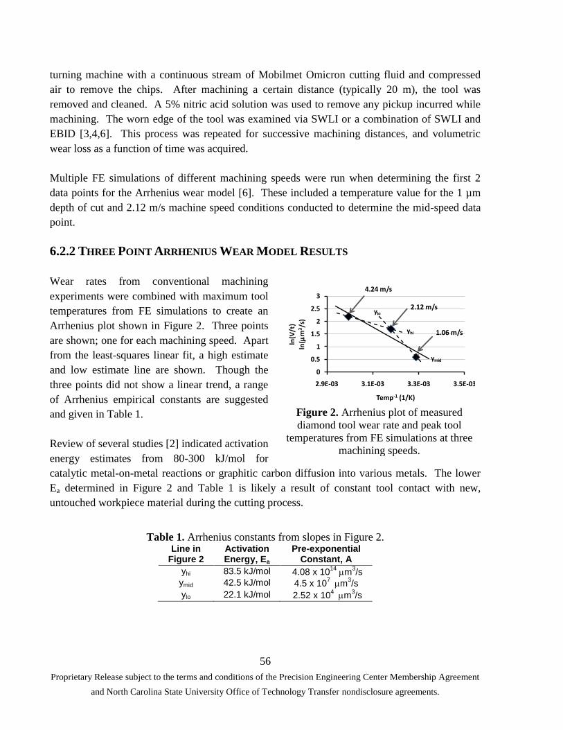
56
Proprietary Release subject to the terms and conditions of the Precision Engineering Center Membership Agreement
and North Carolina State University Office of Technology Transfer nondisclosure agreements.
turning machine with a continuous stream of Mobilmet Omicron cutting fluid and compressed
air to remove the chips. After machining a certain distance (typically 20 m), the tool was
removed and cleaned. A 5% nitric acid solution was used to remove any pickup incurred while
machining. The worn edge of the tool was examined via SWLI or a combination of SWLI and
EBID [3,4,6]. This process was repeated for successive machining distances, and volumetric
wear loss as a function of time was acquired.
Multiple FE simulations of different machining speeds were run when determining the first 2
data points for the Arrhenius wear model [6]. These included a temperature value for the 1 µm
depth of cut and 2.12 m/s machine speed conditions conducted to determine the mid-speed data
point.
6.2.2 THREE POINT ARRHENIUS WEAR MODEL RESULTS
Wear rates from conventional machining
experiments were combined with maximum tool
temperatures from FE simulations to create an
Arrhenius plot shown in Figure 2. Three points
are shown; one for each machining speed. Apart
from the least-squares linear fit, a high estimate
and low estimate line are shown. Though the
three points did not show a linear trend, a range
of Arrhenius empirical constants are suggested
and given in Table 1.
Review of several studies [2] indicated activation
energy estimates from 80-300 kJ/mol for
catalytic metal-on-metal reactions or graphitic carbon diffusion into various metals. The lower
Ea determined in Figure 2 and Table 1 is likely a result of constant tool contact with new,
untouched workpiece material during the cutting process.
Table 1. Arrhenius constants from slopes in Figure 2. Line in
Figure 2 Activation Energy, Ea
Pre-exponential Constant, A
yhi 83.5 kJ/mol 4.08 x 10¹⁴
m3/s
ymid 42.5 kJ/mol 4.5 x 10⁷m
3/s
ylo 22.1 kJ/mol 2.52 x 10⁴m
3/s
Figure 2. Arrhenius plot of measured
diamond tool wear rate and peak tool
temperatures from FE simulations at three
machining speeds.
ylo
yhi
ymid
0
0.5
1
1.5
2
2.5
3
2.9E-03 3.1E-03 3.3E-03 3.5E-03
ln(V
/t)
ln(
m3/s
)
Temp-1 (1/K)
4.24 m/s
2.12 m/s
1.06 m/s

57
Proprietary Release subject to the terms and conditions of the Precision Engineering Center Membership Agreement
and North Carolina State University Office of Technology Transfer nondisclosure agreements.
6.3 EVAM SIMULATIONS
The EVAM machining process is much more
complicated than conventional machining. Tool
temperatures never fully reach a steady state, but
give a cyclic rise and fall while the tool comes in
and out of contact with the workpiece. Again,
tool temperatures are nearly impossible to
measure experimentally for conventional cutting,
let alone EVAM, but can be estimated with FE
modeling. A new elliptical tool vibration mode
in AdvantEdge was developed by ThirdWave to
assist this project. Figure 3 shows an example of
temperature results from an EVAM simulation.
Maximum tool temperature and X (cut) and Y
(thrust) components of tool force vs. time can be
extracted. Results may show how machining
parameters minimize tool wear and optimize
surface finish and/or machining speed.
6.3.1 DATA HANDLING AND WEAR
CALCULATION
AdvantEdge simulations use a variable time step
size in the time integration algorithm. Though
total simulation times are small (< 5x10⁻³
sec for
EVAM frequencies above 10 kHz), time steps are
on the order 10-11
sec. This generates tool force
and temperature data files in excess of 400 Mb.
Normally, AdvantEdge uses TecPlot to plot and
observe simulation data. Large data files require
TecPlot to interpolate data with a high order
polynomial. This allows TecPlot to update plot
displays quickly, but detail is lost in the force and temperature data. A Matlab script was created
that reads in the AdvantEdge datafile and allows the user to subsample the data at a specified
step size. Figure 4 shows a comparison of force data from an AdvantEdge EVAM simulation
against the same data plotted in Matlab. The Matlab plot presents much more detail than
TecPlot.
Figure 3. Example of temperature contour
results from AdvantEdge EVAM
simulation ( 110x20 m ellipse, 10 kHz
vibration, 20m DoC, 0.2 m/s workpiece
speed, diamond tool on St1118 workpiece )
t + 8 sec
t + 16 sec
t + 24 sec
toolchip
tool motion

58
Proprietary Release subject to the terms and conditions of the Precision Engineering Center Membership Agreement
and North Carolina State University Office of Technology Transfer nondisclosure agreements.
Figure 4. Top: TecPlot plot of EVAM simulation data with high-order polynomial interpolation.
Bottom: Matlab plot of same data with 1000 point subsampling and 10 pt running average.
AdvantEdge data from all EVAM simulations
were sub-sampled every 1000 points and stored
in a Matlab array. Force data presented noise
that was about 10% the peak force value, so
was smoothed by a 10 pt running average.
Temperature data had noise less than 1% peak
values and was not smoothed. Temperature
data from EVAM simulations are supplied to
the Arrhenius wear model (Equation (1)) using
the middle estimated Arrhenius constants from
Table 1 (Ea = 42.5 kJ/mol, A = 4.5 x
107m
3/s).
The process for calculating EVAM wear rates
is shown in Figure 5. Since the tool wears only
while in contact with the workpiece, the
average wear rate is determined by integrating
the instantaneous wear rate only over the
contact time, but dividing this value by the total
cycle period:
.
1
ContactAvg Total T
dV dVdt
dt T dt
(2)
Contact time depends on EVAM tool
frequency, workpiece velocity, ellipse shape,
and depth of cut. If the depth of cut (measured
from the workpiece surface to bottom of
Time (s)
Fo
rce
-X(N
),F
orc
e-Y
(N)
0.00096 0.00098 0.001 0.00102
0
20
40
60
Force-X (N)
Force-Y (N)
TecPlot
Matlab
9.6 9.7 9.8 9.9 10 10.1 10.2
x 10-4
0
20
40
60
Fo
rce
- N
Time - sec
Cut Force
Thrust Force
Time (s)
Fo
rce
-X(N
),F
orc
e-Y
(N)
0.00096 0.00098 0.001 0.00102
0
20
40
60
Force-X (N)
Force-Y (N)
TecPlot
Matlab
9.6 9.7 9.8 9.9 10 10.1 10.2
x 10-4
0
20
40
60
Fo
rce
- N
Time - sec
Cut Force
Thrust Force
Figure 5. Top: Example temperature results
for EVAM simulation (same machining
parameters as Figure 3 and Figure 4).
Middle: Expanded temperature profile of one
EVAM cycle.
Bottom: Instantaneous wear rate profile
determined from center image and Arrhenius
wear model.
0 0.2 0.4 0.6 0.8 120
40
60
80
100
Time - ms
Ma
x T
oo
l T
em
pe
ratu
re -
0C
Expanded Section
(Center Image)EVAM Steady State
0 0.02 0.04 0.06 0.08 0.120
30
40
50
60
70
80
Time - ms
Ma
xim
um
To
ol T
em
pe
ratu
re -
0C
Contact
Cooling
0 0.02 0.04 0.06 0.08 0.10
5
10
15
20
25
dV
/dt
-
m3/s
ec
Time - ms
Cooling
Contact
TContact
0 0.02 0.04 0.06 0.08 0.10
5
10
15
20
25
dV
/dt
-
m3/s
ec
Time - ms
Cooling
Contact
0 0.02 0.04 0.06 0.08 0.10
5
10
15
20
25
dV
/dt
-
m3/s
ec
Time - ms
Cooling
Contact0 0.02 0.04 0.06 0.08 0.10
5
10
15
20
25
dV
/dt
-
m3/s
ec
Time - ms
Cooling
Contact
TTotal
(dV/dt) Avg = 3.25 m3/sec
ContactT
dVdt
dt

59
Proprietary Release subject to the terms and conditions of the Precision Engineering Center Membership Agreement
and North Carolina State University Office of Technology Transfer nondisclosure agreements.
ellipse) is larger than the vertical axis of the ellipse, the contact time is approximately 25% of the
ellipse vibration period. Average wear rates were compared for different temperature spikes of
the same EVAM simulation. These calculated wear rates varied less than 3% from spike to spike
during steady state, therefore only one steady state temperature spike is used to calculate average
EVAM wear rates.
6.3.2 SIMULATIONS VARYING HORIZONTAL SPEED RATIO
In the conventional machining simulations, temperature was shown to increase linearly with
workpiece velocity, and logarithmically with depth of cut [6]. In EVAM, the velocity of the
vibrating tool exceeds the workpiece velocity, which cause higher peak tool temperatures.
Higher workpiece velocities also create larger chips if the EVAM frequency is kept constant,
which in turn create higher temperature. The horizontal speed ratio (HSR) relates the peak
EVAM ellipse speed to the workpiece velocity. It is typically related to PV surface finish [7],
but it also determines the relative EVAM chip size, as shown in Figure 6.
wkpcvHSR
a (3)
Figure 6. Relation of horizontal speed ratio to EVAM chip size
It is estimated that the dual contribution of speed and chip size to tool temperature creates a
nonlinear increase to EVAM tool temperature vs. workpiece velocity (or HSR) for a constant
frequency. It’s further estimated that this creates a specific HSR in which the average wear rate
of the EVAM tool will be greater than if conventional machining were done. To test these
hypotheses, EVAM simulations were created in AdvantEdge that varied only workpiece velocity
and thereby HSR. Simulation parameters are given in Table 2. Equivalent conventional cutting
simulations were also created with the same workpiece velocity and depth of cut for a total of 8
simulations.
ellipsev a
wkpcv
Uncut chip
1st tool pass 2nd tool pass
Low HSR (<1%) High HSR (>10%)
Workpiece surface

60
Proprietary Release subject to the terms and conditions of the Precision Engineering Center Membership Agreement
and North Carolina State University Office of Technology Transfer nondisclosure agreements.
Table 2. Simulation parameters for 4 EVAM and 4 conventional cutting simulations
EVAM Frequency 10 kHz
Ellipse Shape 110 x 20 µm
Depth of Cut 40 µm
Workpiece Velocity 0.1, 0.2, 0.6, 1 m/s
Tool Material Single Crystal Diamond
Workpiece Material AISI 1118 Steel
FEM Results of Varying Horizontal Speed Ratio
Temperature profiles from the EVAM simulations are shown in Figure 7. Temperature profiles
are shifted such that the same time points of the ellipse trajectories are aligned on the X axis.
Temperature increases sooner for higher HSRs since the tool enters the workpiece at an earlier
point on the ellipse which increases the overall contact time.
Figure 7. Maximum simulated EVAM tool temperatures for varying horizontal speed ratios.
Peak EVAM tool temperatures were much
higher than their conventional machining
equivalent due to the increased tool tip
velocity. Average EVAM tool temperature
was determined by integrating temperature
profiles in Figure 7 over one EVAM period
(0.1 ms). These average temperatures are
compared against steady state non-EVAM
tool temperatures, shown in Figure 8.
Average EVAM temperatures were higher
than conventional temperatures for all but
the highest workpiece velocity or HSR.
-0.04 -0.02 0 0.02
20
40
60
80
100
120
140
Time - ms
Ma
xim
um
To
ol T
em
p. -
oC
HSR = 1.4%
HSR = 2.9%
HSR = 8.7%
HSR = 14.5%
Figure 8. Steady state temperatures from
conventional machining simulations and average
EVAM too temperatures.
conv = 38.229V + 20R² = 0.9857
EVAM = 13.361ln(HSR) + 19.738R² = 0.9985
0 5 10 15
0.0
10.0
20.0
30.0
40.0
50.0
60.0
70.0
0 0.25 0.5 0.75 1 1.25
HSR %
Tem
pe
ratu
re C
Workpiece Velocity (m/s)
Conventional
EVAM Avg.
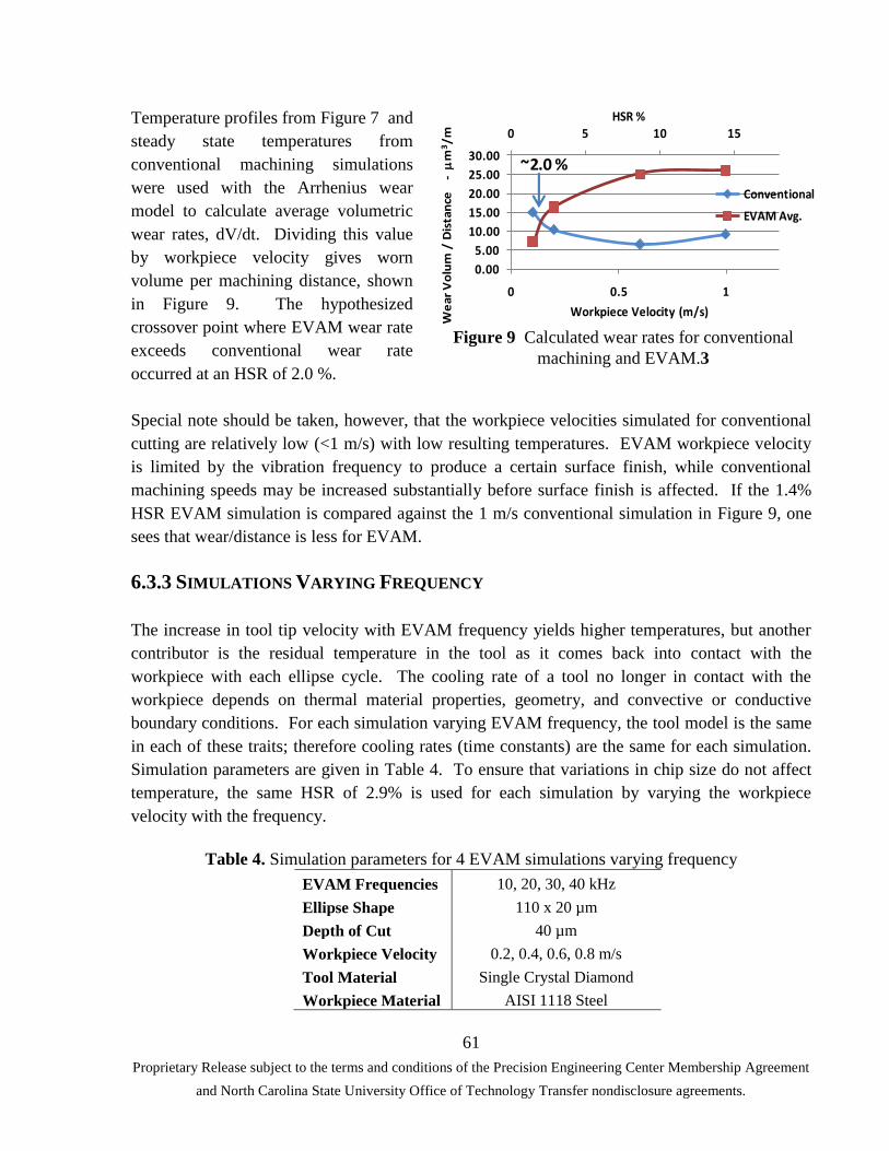
61
Proprietary Release subject to the terms and conditions of the Precision Engineering Center Membership Agreement
and North Carolina State University Office of Technology Transfer nondisclosure agreements.
Temperature profiles from Figure 7 and
steady state temperatures from
conventional machining simulations
were used with the Arrhenius wear
model to calculate average volumetric
wear rates, dV/dt. Dividing this value
by workpiece velocity gives worn
volume per machining distance, shown
in Figure 9. The hypothesized
crossover point where EVAM wear rate
exceeds conventional wear rate
occurred at an HSR of 2.0 %.
Special note should be taken, however, that the workpiece velocities simulated for conventional
cutting are relatively low (<1 m/s) with low resulting temperatures. EVAM workpiece velocity
is limited by the vibration frequency to produce a certain surface finish, while conventional
machining speeds may be increased substantially before surface finish is affected. If the 1.4%
HSR EVAM simulation is compared against the 1 m/s conventional simulation in Figure 9, one
sees that wear/distance is less for EVAM.
6.3.3 SIMULATIONS VARYING FREQUENCY
The increase in tool tip velocity with EVAM frequency yields higher temperatures, but another
contributor is the residual temperature in the tool as it comes back into contact with the
workpiece with each ellipse cycle. The cooling rate of a tool no longer in contact with the
workpiece depends on thermal material properties, geometry, and convective or conductive
boundary conditions. For each simulation varying EVAM frequency, the tool model is the same
in each of these traits; therefore cooling rates (time constants) are the same for each simulation.
Simulation parameters are given in Table 4. To ensure that variations in chip size do not affect
temperature, the same HSR of 2.9% is used for each simulation by varying the workpiece
velocity with the frequency.
Table 4. Simulation parameters for 4 EVAM simulations varying frequency
EVAM Frequencies 10, 20, 30, 40 kHz
Ellipse Shape 110 x 20 µm
Depth of Cut 40 µm
Workpiece Velocity 0.2, 0.4, 0.6, 0.8 m/s
Tool Material Single Crystal Diamond
Workpiece Material AISI 1118 Steel
Figure 9 Calculated wear rates for conventional
machining and EVAM.3
0 5 10 15
0.00
5.00
10.00
15.00
20.00
25.00
30.00
0 0.5 1
HSR %
We
ar V
olu
m /
Dis
tan
ce
-
m3/m
Workpiece Velocity (m/s)
Conventional
EVAM Avg.
~2.0 %

62
Proprietary Release subject to the terms and conditions of the Precision Engineering Center Membership Agreement
and North Carolina State University Office of Technology Transfer nondisclosure agreements.
The wear of the tool may be exacerbated by the increased residual tool temperature and
increased heat flux due to faster tip velocities. Higher frequencies, however, allow faster
machine time. Understanding the relationship between wear and frequency will allow for an
optimal operation point given the benefits of faster machine time vs. the detriment of higher wear
rates.
FEM Results of Varying Frequency
Figure 10 shows the temperature results for the 4 EVAM simulations varying frequency. As
expected, higher frequencies resulted in higher peak temperatures. Average temperature was
determined by integrating the temperature curves after reaching steady state and dividing by
time. Residual temperature was determined by measuring temperature just before the tool makes
contact with the workpiece.
Figure 10. Left: Simulated maximum tool temperature profiles for different EVAM frequencies.
Right: Results of different components of the temperature profiles.
Temperature profiles were again supplied to the Arrhenius wear model as done with the HSR
simulations, and average wear rate was determined using equation(2). These average wear rate
results are shown in Figure 11, left. These values were divided by workpiece velocity to get
wear volume per machining distance, shown in Figure 11, right. The wear per time increased
with the frequency squared while the wear per distance increased linearly with frequency.
Figure 11. Left: Average wear rate (volume loss per time) for varying frequencies. Right: Wear
per machining distance.
50
100
150
50
100
150
Ma
xim
um
To
ol T
em
pe
ratu
re -
oC
50
100
150
0 0.05 0.1 0.15 0.2
50
100
150
Time - ms
20
60
100
140
180
0 10 20 30 40 50
Tem
pe
ratu
re (0 C
)
Frequency (kHz)
Peak Temperature Average TemperatureResidual Temperature
dV/ds = 0.0016fR² = 0.9965
0
0.02
0.04
0.06
0.08
0 20 40 60
We
ar V
olu
em
/ C
ut
Dis
tan
ce (
m3 /
m)
Frequency (kHz)
dV/dt = 0.0298f2.0188
R² = 0.9996
0
10
20
30
40
50
60
0 20 40 60
Ave
rage
We
ar R
ate
(m
3 /s)
Frequency (kHz)

63
Proprietary Release subject to the terms and conditions of the Precision Engineering Center Membership Agreement
and North Carolina State University Office of Technology Transfer nondisclosure agreements.
6.3.4 SIMULATIONS VARYING ELLIPSE SHAPE
The history of EVAM research includes individual analyses of horizontal, circular, or vertically
oriented elliptical toolpaths. Researchers preferring the horizontal ellipse shape (including the
PEC) extol the ability to machine at higher speeds while maintaining an adequate surface finish.
Proponents of the vertically oriented elliptical cutting claim the upward motion of the tool assists
in lifting the chip out from the workpiece, thereby creating a net zero or negative thrust force on
the tool and reducing wear [1]. A direct comparison is complicated by the relationships between
ellipse shape, workpiece velocity, frequency, surface finish, and uncut chip shape.
In order to observe the effects of varying ellipse shape, some EVAM parameters need to remain
constant. Ultimately, the desired result of using EVAM is to maintain an adequate surface finish
over the longest machining distance, therefore a constant theoretical surface finish is maintained
in the EVAM-FEM models. Theoretical surface using EVAM depends on the machining speed,
frequency, and ellipse curvature in the same manner that surface finish in conventional turning
depends on cross-feed and tool radius. An approximated calculation of PV surface finish is
given: 2
18 8
wkpc wkpcv vfeed bPV for HSR
R fa a
(4)
This equation shows that for an ellipse shape determined by axis amplitudes a and b, the
workpiece velocity vwkpc and tool vibration frequency f must change proportionally with one
another to maintain a constant PV surface finish. Three other parameters are maintained
constant to fully define EVAM simulation: depth of cut, vibration frequency and ellipse included
area. Depth of cut is set larger than the largest vertical amplitude so that tool motion in each
simulation completely undercuts the workpiece surface.
Table 5. Machining parameters for 3 EVAM-FEM models varying ellipse shape.
EVAM Frequency 20 kHz
Ellipse Shapes, axb
Ellipse Aspect Ratio, r = a/b
56.6x11.3 µm, 25.3x25.3 µm, 11.3x56.6 µm
5.01, 1.00, 0.20
Depth of Cut 60 µm
Workpiece Velocity
Theoretical PV
0.237, 0.07, 0.02 m/s
58 nm
Tool Material Single Crystal Diamond
Workpiece Material AISI 1118 Steel
Using these input values, the relative effects of varying ellipse shape are calculated for multiple
other machining parameters. These resulting parameters are normalized against the maximum

64
Proprietary Release subject to the terms and conditions of the Precision Engineering Center Membership Agreement
and North Carolina State University Office of Technology Transfer nondisclosure agreements.
value in the range to observe the relative effect from ellipse ratio has. Results are shown in
Figure 12. It is noteworthy that the sliding distance per upfeed decreases as the ellipse ratio
increases. When this ratio is multiplied by the total cutting distance, it gives the total distance
over which the tool was in contact with the workpiece. Therefore, horizontally inclined ellipses
allow the tool to contact the workpiece less than vertical ellipses for the same total cutting
distance.
Figure 12. Normalized machining parameters calculated from EVAM input parameters
Based on these calculations, it was estimated that the horizontal ellipse models would result in
greater chemical wear per EVAM cycle. Increased chip area, workpiece velocity, and sliding
distance per cycle contribute to higher tool temperatures and forces for each EVAM cycle.
However, the resulting higher rates of wear per cycle may not necessarily mean greater amounts
of wear over the same total machining distance. The higher temperatures ensured by the
horizontal ellipse are balanced by the increased machining speed, which allows the tool to be in
contact with the workpiece for less total time. Therefore, the effect ellipse shape will have on
wear cannot be estimated solely based on kinematic calculations, but require the thermo-
mechanical response available through FEM.
FEM Results of Varying Ellipse Shape
Tool forces and temperatures were extracted from the three AdvantEdge simulations using the
method described in section 6.3.1. Figure 13 shows the cut and thrust force for the each
simulation. Overall forces tended to increase as the ellipse became horizontal; a result of the
increasing uncut chip area described in Figure 12.

65
Proprietary Release subject to the terms and conditions of the Precision Engineering Center Membership Agreement
and North Carolina State University Office of Technology Transfer nondisclosure agreements.
Figure 13. Cut (Fx) and thrust (Fy) forces for varying ellipse shapes over one 20kHz cycle.
The amount of time that the tool experiences negative thrust force was smallest for the horizontal
ellipse shape, although all three ellipse shapes exhibited some negative thrust. Thrust forces for
the vertical ellipse were negative for almost the entire vibration cycle, indicating a continuous
state of ‘lifting’ the chip from the workpiece. Though this reduces the overall tool force, tool
temperature likely has a greater effect on wear, as described in section 6.1. Figure 14 shows
results of maximum tool temperature for one EVAM cycle and the estimated wear rate based on
these temperatures and the Arrhenius wear model. The horizontal ellipse shape resulted in
highest peak temperatures due to the higher tool tip velocity and chip size. Average wear rates
were also calculated using Equation(2). Table 6 summarizes these values.
Figure 14. FEM results of maximum tool temperature (left) and calculated wear rate based on
Arrhenius model (right) for varying EVAM ellipse shapes.
0.5 1 1.5 2 2.5
x 10-5
0
50
100
Time
Fo
rce
- N
11x56m Fx
11x56m Fy
25x25m Fx
25x25m Fy
56x11m Fx
56x11m Fy
0 1 2 3 4 5
x 10-5
20
30
40
50
60
70
Time - sec
Te
mp
era
ture
- o
C
11x56m
25x25m
56x11m
1 2 3 4 5
x 10-5
2
4
6
8
10
12
14
Time - s
We
ar
Ra
te -
m
3/s
ec
11 x 56 m
25 x 25 m
56 x 11 m

66
Proprietary Release subject to the terms and conditions of the Precision Engineering Center Membership Agreement
and North Carolina State University Office of Technology Transfer nondisclosure agreements.
Table 6. Calculated temperature and estimated Arrhenius wear from EVAM FEM models with
varying ellipse shape.
Ellipse Shape,
Ratio
Peak Tool
Temperature - oC
Average Tool
Temperature - oC
Average
Wear Rate –
m3/sec
Wear Volume /
Machining Distance –
m3/m
11x56 m r = 0.2 59.5 28.3 1.30 63.7
25x25 m, r = 1 52.6 29 1.35 19.29
56x11 m, r = 5 70.8 34 2.46 10.38
The average wear rate measured in volume of diamond loss per time was greatest for the horizontal
ellipse (56x11 m, r = 5) simulation. As previously mentioned, this indicates a more aggressive cut
during each EVAM cycle based on the higher forces and temperature. However, due to the increased
machining speed, the total wear volume per machining distance is least for the horizontal ellipse. This
shows that the benefit of increased machining speed outweighs the effects of a more aggressive EVAM
cutting cycle when surface finish is constant.
6.4 EVAM EXPERIMENTS VARYING FREQUENCY
Two of the three EVAM parameters modeled in FEA (frequency and ellipse shape) will also be
varied through cutting experiments. The EVAM cutting device at the PEC, called the Ultramill,
is capable of operating between 1-4 kHz. Though HSR could be varied experimentally, this
would require conventional machining speeds on the order of 2-8 mm/s for a similar comparison
to Figure 9. The following gives results of EVAM experiments varying frequency. Further
experiments varying ellipse shape are planned for the future.
6.4.1 EXPERIMENT SETUP
The first design of the Ultramill included a ceramic toolholder with two base grooves. These
grooves pivoted on ceramic half-cylinders that were attached to piezoelectric stack actuators.
Machining with the Ultramill caused compressive stress on the rear groove, forcing the groove to
open and form a crack along its length. Also, the half-cylinder / groove contacts were
kinematically over constrained, causing potential for contact loss. A new toolholder shown in
Figure 15 was designed for the Ultramill that incorporates a thicker base with one groove and
flat. Also shown is the relationship between the elliptical toolpath and the kinematic linkage to
the piezoelectric stack actuators.

67
Proprietary Release subject to the terms and conditions of the Precision Engineering Center Membership Agreement
and North Carolina State University Office of Technology Transfer nondisclosure agreements.
Figure 15. New flat+groove Ultramill toolholder design and kinematic linkage for elliptical
toolpaths
Orthogonal cutting geometry was used for the EVAM experiments where the direction of cutting
is parallel to the rake face normal. A 0.25mm wide by 41 mm long fin was machined into a
piece of AISI1215 steel and a central hole allowed the workpiece to be mounted on a 3-axis
piezoelectric load cell. A straight-edged, 0o rake, 6
o clearance synthetic diamond tool was
mounted to the ceramic Ultramill toolholder. The 2.28 mm width of the tool allowed the
workpiece to contact in 4 distinct wear zones, shown in the front view of Figure 16. One zone
was utilized to initially machine the surface of the fin so that consequent machining is done on a
flat surface and there is no variation in the depth of cut. Three other zones were defined for
EVAM machining at 1, 2, and 4 kHz.
Figure 16. Schematic of AISI 1215 steel fin workpiece, cutting orientation, and wear zones on
the tool for EVAM wear experiments varying frequency.
time
dis
pla
cem
en
t
RakePiezoStack
Flank PiezoStack
Elliptical Tool Tip Motion
FlankRake
New flat+groovedesign
Ultramill toolholder w/ straight-edged diamond
Kistler 3-axis load cell
0.25 mm wide fin
Fla
tten
fin
1 k
Hz
2 kH
z
4 k
Hz
Rake Face of Tool
Fin
Workpiece and Ultramill Setup Cutting Zones on Tool
0.25 mm
2.28 mm

68
Proprietary Release subject to the terms and conditions of the Precision Engineering Center Membership Agreement
and North Carolina State University Office of Technology Transfer nondisclosure agreements.
A Lion Precision air bearing LVDT was used to measure the alignment of the workpiece about
the center screw and the pitch in the cutting direction. The fin was aligned about the center
screw to within 5 m over the 41 mm fin length. This ensures that the width of the wear zones is
nominally the same width as the fin. The pitch of the fin in the cutting direction was measured
and compensated for in the CNC program.
The fin was initially cut using the ‘flatten fit’ section of the tool noted in Figure 16. A constant
drip (~1 drop/sec) of Mobilmet Omicron cutting fluid was used so that the cutting region was
continuously covered. Touchoff was accomplished by advancing the tool toward the workpiece
in 100 nm increments and measuring changes to the force signal from the load cell. After initial
touchoff, a CNC program was run that cut the 41 mm length of the fin incrementing down with 2
m depth of cut. A total of 120 passes were completed for a total machining distance of 5.13 m.
Tool forces measured from the load cell were acquired every 20 passes. After the CNC program
ended the workpiece was then removed from the machine and surface finish was measured. The
cutting and workpiece measuring process was repeated on the same fin for 2 kHz and 4 kHz
using the corresponding locations on the tool edge (Figure 16). Similarly to FEM simulations,
workpiece velocity was increased to match the EVAM frequency and preserve a constant uncut
chip shape. Table 7 gives corresponding velocities and constant parameters defined by the uncut
chip shape.
Table 7. EVAM machining parameters for cutting experiments varying frequency
EVAM
Frequency
Workpiece
Velocity
Total Machining Time
(including non-cutting passes)
Total Contact Time
1 kHz 2 mm/s 1 hr 40 min 10 min 47sec
2 kHz 4 mm/s 55 min 5 min 23 sec
4 kHz 8 mm/s 32 min 2 min 42 sec
Constant Parameters:
Ellipse Shape = 11 x 2 m (horizontal) Horizontal Speed Ratio = 2.89 %
Upfeed per cycle = 2 m Depth of Cut = 2 m
Theoretical PV Surface Finish = 8 nm Sliding Distance / Cycle = 13.0 m
Sliding Distance / Upfeed Ratio = 6.49 Duty Cycle (% contact) = 25.9 %
Two particular parameters of interest are the sliding distance / upfeed ratio and the duty cycle.
The sliding distance / upfeed ratio tells how far the tool slides against the workpiece per distance
the workpiece travels. Multiplying this ratio by the machining distance (5.13 m) gives you the
real distance over which the tool contacts the workpiece (33.30 m). The duty cycle tells what
percentage of the EVAM cycle the tool is actually in contact with the workpiece. Multiplying
this by the machining distance over workpiece velocity gives the total time the tool is contacting
the workpiece.

69
Proprietary Release subject to the terms and conditions of the Precision Engineering Center Membership Agreement
and North Carolina State University Office of Technology Transfer nondisclosure agreements.
6.4.1 SURFACE FINISH
After each 5m cut distance, the workpiece fin was observed in a Zygo NewView scanning white
light interferometer (SWLI). Figure 17 compares a surface finish measurement from the
conventional machining experiments mentioned in Section 6.2 with one obtained from the
EVAM experiments. The steel surface after conventional machining was dominated by grooves
in the cutting direction likely caused by dragging of hard alloying inclusions through the metal.
The EVAM surfaces did not display this dragging, but exhibited inclusions ‘stuck’ into the
surface. The absence of dragging was seen in all of the measured EVAM surfaces, each of
which had consistent surface finish of < 15nm Ra.
Figure 17. Conventional machining surface finish vs 1kHz EVAM surface finish on AISI 1215
steel.
Figure 18 shows a cross-section slice from the horizontal line of the surface in Figure 17 right.
This slice covers one of the alloy inclusions, which has a height of approximately 60 nm.
Though visible in the SWLI surface plot, these inclusions contributed little to the overall surface
finish due to their relatively small heights.
Figure 18. 2D surface slice from horizontal line in Figure 17, right shows height of inclusion.
677 nm
-838 nm
Cu
t d
ire
ctio
n
344 nm
-350 nm
Cut direction
20 m 20 m
AISI 1215 Steel, Conventional Machining40 m machining distance Ra = 122 nm
AISI 1215 Steel, 1 kHz EVAM5 m machining distance Ra = 7 nm
20 m
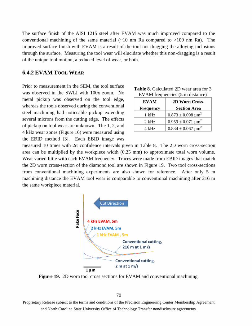
70
Proprietary Release subject to the terms and conditions of the Precision Engineering Center Membership Agreement
and North Carolina State University Office of Technology Transfer nondisclosure agreements.
The surface finish of the AISI 1215 steel after EVAM was much improved compared to the
conventional machining of the same material (~10 nm Ra compared to >100 nm Ra). The
improved surface finish with EVAM is a result of the tool not dragging the alloying inclusions
through the surface. Measuring the tool wear will elucidate whether this non-dragging is a result
of the unique tool motion, a reduced level of wear, or both.
6.4.2 EVAM TOOL WEAR
Prior to measurement in the SEM, the tool surface
was observed in the SWLI with 100x zoom. No
metal pickup was observed on the tool edge,
whereas the tools observed during the conventional
steel machining had noticeable pickup extending
several microns from the cutting edge. The effects
of pickup on tool wear are unknown. The 1, 2, and
4 kHz wear zones (Figure 16) were measured using
the EBID method [3]. Each EBID image was
measured 10 times with 2 confidence intervals given in Table 8. The 2D worn cross-section
area can be multiplied by the workpiece width (0.25 mm) to approximate total worn volume.
Wear varied little with each EVAM frequency. Traces were made from EBID images that match
the 2D worn cross-section of the diamond tool are shown in Figure 19. Two tool cross-sections
from conventional machining experiments are also shown for reference. After only 5 m
machining distance the EVAM tool wear is comparable to conventional machining after 216 m
the same workpiece material.
Figure 19. 2D worn tool cross sections for EVAM and conventional machining.
4 kHz EVAM, 5m
2 kHz EVAM, 5m
1 kHz EVAM , 5m
1 m
Conventional cutting, 216 m at 1 m/s
Conventional cutting, 2 m at 1 m/s
Cut Direction
Rak
e F
ace
Table 8. Calculated 2D wear area for 3
EVAM frequencies (5 m distance)
EVAM
Frequency
2D Worn Cross-
Section Area
1 kHz 0.873 ± 0.098 µm2
2 kHz 0.959 ± 0.071 µm2
4 kHz 0.834 ± 0.067 µm2

71
Proprietary Release subject to the terms and conditions of the Precision Engineering Center Membership Agreement
and North Carolina State University Office of Technology Transfer nondisclosure agreements.
Though machining distance was different for the EVAM experiments and 216 m conventional
experiment, the total contact time is comparable. The real contact distance of the EVAM tool
was 33.3 m with contact times between 2.7-10.8 min. The 216 m conventional tool had a contact
time of 3.6 min, while the 2 m conventional tool only contacted for 2 sec.
6.5 CONCLUSIONS
A chemical wear model was developed based on the Arrhenius equation. Wear measurements
made during conventional DT of St1215 were coupled with tool temperatures obtained from FE
simulations to construct an Arrhenius plot. The proposed activation energy is in the range of 22-
83 kJ/mol. This is relatively low compared to metal-on-metal diffusive processes. The constant
removal of diamond in addition to a catalytic relationship between diamond and ferrous
workpiece are likely reasons for this low activation energy.
FE simulations of EVAM cutting completed varying horizontal speed ratio, tool vibration
frequency, and ellipse shape. Simulated tool temperatures were coupled with the Arrhenius wear
model to determine average EVAM wear rates. It was found that at a certain value of HSR, the
wear of an EVAM tool with respect to machining distance exceeds that of conventional
machining when assuming the Arrhenius model. From simulations varying frequency it was
found that increasing the EVAM frequency while maintaining the same HSR causes a linear
increase of tool wear per machining distance with increased frequency. Simulations varying
ellipse shape showed that horizontally ellipses (aligned with the cutting direction) generate
higher forces, temperature, and wear pear each vibration cycle. However, horizontal ellipses
allow higher machining speeds to maintain the same theoretical surface finish. This higher
machine speed results in less wear per machining distance for the horizontally aligned EVAM
ellipse.
EVAM experiments were conduction that varied vibration frequency while maintaining the same
HSR. After 5m machining distance, EVAM frequencies at 1, 2, and 4 kHz yielded the same
amount of wear. The experiment needs to continue at further machining distances to relate to
results found from FE models. The EVAM tool wear at 5 m was comparable to conventional
machining at 216 m, and far greater than conventional machining after 2 m. This shows that
EVAM did not reduce tool wear over the same machining distance, but does result in a similar
amount of wear related to contact time. Despite excessive tool wear, EVAM yielded a
dramatically better surface finish. This is primarily due to the absence of particle dragging
through the workpiece surface, which dominates the surface structure of conventionally
machined steel. Another contribution to surface finish improvement may come from metal
pickup on the tool which was observed after conventional machining but not EVAM.

72
Proprietary Release subject to the terms and conditions of the Precision Engineering Center Membership Agreement
and North Carolina State University Office of Technology Transfer nondisclosure agreements.
REFERENCES
1. Brehl DE, Dow TA. Review of Vibration-Assisted Machining, Precision Engineering. 2008;
32: 153-172.
2. Paul E, Evans CJ, Mangamelli A, McGlauflin ML, Polvani RS, Chemical Aspects of Tool
Wear in Single Point Diamond Turning, Precision Engineering. 18; 4-19
3. Shi M, Lane B, Mooney CB, Dow TA, Scattergood R, Diamond Tool Wear Measurement by
Electron-beam-induced Deposition, Precision Engineering. 2010; Article in press.
4. Lane B, Development of Predictive models for Abrasive and Chemical Wear of Diamond
Tools, MS Thesis, North Carolina State Univesity, 2010
5. Negishi N, Elliptical Vibration Assisted Machining with Single Crystal Diamond Tools, MS
Thesis, North Carolina State University, 2003.
6. Lane B, Dow TA, Scattergood R, Diamond Tool Wear Improvements with Elliptical
Vibration Assisted Machining, Precision Engineering Center Annual Report, 2010
7. Cerniway M, Elliptical Diamond Milling: Kinematics, Force, and Tool Wear, MS Thesis,
North Carolina State University, 2001

73
Proprietary Release subject to the terms and conditions of the Precision Engineering Center Membership Agreement
and North Carolina State University Office of Technology Transfer nondisclosure agreements.
7 VISUALIZATION OF CHIP SHAPE AND MACHINING
FORCES
Darrell LaBarbera
Graduate Student
Thomas A. Dow
Professor, Mechanical and Aerospace Engineering
The goal is this project was to develop a method to measure the cutting forces at the same time
the chip shape was measured. These two tasks have been done separately by a number of
investigators, but performing them simultaneously will provide increased understanding of the
chip pickup problem. Under certain cutting conditions, the workpiece material becomes
attached to the cutting tool resulting in much higher tool forces and poor surface finish. The
onset of this phenomenon may be due to lubrication breakdown and/or chemical affinity of the
tool and workpiece. The particular emphasis is diamond turning where a single-crystal diamond
tool is used to machine different types of steel. Under some conditions it is virtually impossible
to machine the surface because of huge changes in the force (factor of 10). Tool cutting and
thrust forces and chip shape have been recorded for depths of cut from 7 to 25 μm on aluminum
and steel workpieces. Images of the chips at each depth of cut were collected with sufficient
visual clarity to see the chip formation. Higher magnification and faster shutter speed will be
required to see shear bands or the actual pickup of material on the tool. Machining experiments
using 1010 steel were performed at 7 and 10 μm depths of cut with carbide and diamond tools.
The diamond tool produced a smooth clean chip while the carbide tool produced a discontinuous
chip. The discontinuity of the chip was used to explain the variable forces observed with the
carbide tool.

74
Proprietary Release subject to the terms and conditions of the Precision Engineering Center Membership Agreement
and North Carolina State University Office of Technology Transfer nondisclosure agreements.
7.1 INTRODUCTION
Precision machining, using a diamond tool or a diamond grinding wheel, can be used to create
surfaces with optical quality figure error (< 150 nm) and surface finish less than 5 nm RMS. The
detailed shape of the diamond tool or grinding wheel grit has a profound influence on both of
these figures of merit. There has been a wealth of information generated by researchers related
to the tool shape, the workpiece material, lubrication and the forces in the cutting and thrust
direction. For diamond machinable materials (hard copper, brass, aluminum and some ceramic
materials), the cutting process is very stable and the chips and forces are constant for long
periods of time, sometimes for many days. However, there are other materials that are not
typically machined with diamond tools, such as steel, and the cutting process is anything but
stable. Knowledge of the material flow and the parameters that influence it are important to
improve the shape and surface finish of new materials.
The cutting forces generated during diamond turning are a function of the shape and rake angle
of the tool, the depth of cut, the friction on the rake and flank faces and the machining speed.
Simulations of the cutting process [1] use a complex material model to predict the flow of
material over/under the tool based on yield stress, shear rate, temperature and many other
material properties. The result is a picture of the flow, the predicted cutting force (in the cutting
direction), thrust force (normal to the cutting direction) as well as temperature in both the tool
and the chip.
The goals of this project are to bring together measurements of tool forces, images of chip flow
and predictions of temperature and material response in precision machining. This will require
measurement of the machining forces, high speed photography as well as thermal modeling and
measurement.
7.2 MACHINING EXPERIMENTS
One important issue that the cutting models do not address is the potential of material pickup on
the cutting edge of the tool. This phenomenon changes the flow field, the forces and the surface
finish of the workpiece. Visualization of the chip has improved the understanding of the pickup
process and how it changes with machining conditions and tool geometry [2-4]. The goal of this
project is to use equipment available in the PEC to demonstrate the tool forces and chip shape
that results in machining steel and aluminium workpieces. This report describes the
experimental apparatus, the experiments performed and the results.

75
Proprietary Release subject to the terms and conditions of the Precision Engineering Center Membership Agreement
and North Carolina State University Office of Technology Transfer nondisclosure agreements.
7.2.1 EXPERIMENTAL SETUP
Figure 1: Slow Speed Turning Setup
Figure 1 shows the DTM with the force sensor and visualization system as well as the stepper
motor and belt needed for the slow speed required. The stepper motor is attached to the machine
frame and the belt drives the OD of the vacuum chuck. This system was capable of turning the
lathe vacuum chuck down to 0.05 rpm or approximately 0.33 mm/s at the tool. The tool was fed
from left to right and the microscope was mounted on the same slide so it stays focused on the
tool.
For the cutting experiments, a flat nose diamond tool was used and the workpiece was narrower
than the tool producing orthogonal cutting. For the aluminum tests, the workpiece was a thin
circular sheet with a diameter of 129.3 mm and a thickness of 0.77 mm. This sheet was clamped
between two cylinders for support and less than 10 mm extended from the clamping cylinders.
The cutting experiments using 6061-T6 aluminium are all performed at 0.02 revolutions per
second of the stepper motor or 0.16 rpm for the lathe spindle. The linear velocity of the
workpiece was 1.08 mm/sec.
The face of the thin workpiece was machined so that it was cylindrical and centered. Then the
stepper motor was set to rotate at 0.02 revolutions per second. The tool was then plunged into
the workpiece at 0.1 mm/min while the workpiece rotated. Two depths of cut were studied, 10
and 25 µm. With the infeed speed used, the two depths of cut were reached in 6 and 15 seconds,
respectively, as shown on the force plots. The cutting time was set not to exceed one revolution
of the workpiece or 6 minutes and 15 seconds. Each time the experiment was restarted the
workpiece was refaced. The aluminum experiments were designed to show what can be
visualized with the microscope and camera available at the PEC.

76
Proprietary Release subject to the terms and conditions of the Precision Engineering Center Membership Agreement
and North Carolina State University Office of Technology Transfer nondisclosure agreements.
The cutting experiments for 1010 steel were all performed at 0.08 rpm for the lathe spindle. The
thickness of the steel disk was 0.49 mm and the diameter was 128.2 mm. The linear velocity of
the workpiece was 0.54 mm/sec. These experiments began, as with the aluminum material, by
facing the cutting surface so that it was circular. Each time the experiment was restarted the
workpiece was refaced. Two tools materials were used for the steel machining experiments,
carbide and single-crystal diamond.
7.2.2 EXPERIMENTAL RESULTS
ALUMINUM 6061-T6 - 10 µm DEPTH OF CUT
Figure 2: Chip image for 10μm depth of cut
Figure 2 shows the chip generated at a 10μm depth of cut and Figure 3 shows the associated
forces. The average cutting force was 8.1 N and the thrust force was 4.7 N. The picture in
Figure 2 corresponds to the vertical line on Figure 3 with respect to the time. For constant
infeed, the depth of cut increases as time increases until it reaches the desired depth. Figure 3
shows the cutting force (Fz top) and the thrust force (Fx bottom) as a function of the machining
time. Both forces increase in a similar manner as the tool moves into contact with the
workpiece. As tool moves into the workpiece and a chip is formed, the thrust force reaches an
asymptote related to the geometry of the tool and the properties of the workpiece. The thrust
force does not change but as the depth of cut continues to increase; the cutting force grows larger
until the desired depth of cut is reached. For the 10 μm depth of cut and an infeed rate of 0.1
mm/min, it should take 6 seconds to reach the nominal depth. The dotted line on Figure 3 shows
about 6 seconds from the start of cutting to achieve steady-state operation.
Tool Cutting direction

77
Proprietary Release subject to the terms and conditions of the Precision Engineering Center Membership Agreement
and North Carolina State University Office of Technology Transfer nondisclosure agreements.
Figure 3: Tool forces machining 6061-T6 aluminum at 10 μm depth of cut
ALUMINUM 6061-T6 - 25µm DEPTH OF CUT
Figure 4: Diamond Tool 25μm Depth of Cut Picture
Figure 4 shows an aluminum workpiece at a 25 μm depth of cut. Figure 5 shows the forces
collected during this experiment. This force curve clearly shows the increase in force as the tool
plunges into the workpiece at 0.1 mm/sec. As in Figure 3, the thrust force achieves its maximum
value before the cutting force. The thrust force is less dependent on the depth of cut and more on
the tool geometry. The average cutting force was 18.3 N and the average thrust force was 10.3

78
Proprietary Release subject to the terms and conditions of the Precision Engineering Center Membership Agreement
and North Carolina State University Office of Technology Transfer nondisclosure agreements.
N. The picture in Figure 4 is representative of the vertical line at 58 seconds in Figure 5 and
shows the forces at that point in time.
Figure 5: Tool forces when machining 6061-T6 aluminum at 25 μm depth of cut
Figure 6 shows the results for the 10 μm depth of cut performed on 1010 steel. The force data
has been filtered to reduce the high-frequency features and show the main fluctuations in force
over the experiment. There are two large drops in both the cutting force and the thrust force at
65 and 125 seconds. The chip image shows a kink in the chip that occurs when this drop occurs.
It may be pickup of steel on the tool that makes the force rise and then expulsion of that pickup
that creates the drop. More experiments are needed to study the pickup process.
7.3 CONCLUSIONS
Cutting experiments using aluminum have been performed for depths of 10μm and 25μm.
Images of the chips at each depth of cut were collected with sufficient visual clarity to see the
chip formation. Higher magnification of the chip images and higher speed collection will be
required to see shear bands or pickup of material on the tool.
Machining experiments using 1010 steel were performed at 7 and 10 μm depths of cut. This
steel was machined with carbide and diamond tools. The diamond tool produced a smooth clean
chip while the carbide tool produced a discontinuous chip. The discontinuity of the chip explains
the fluctuating forces observed with the carbide tool. With higher image magnification,
visualizing the cause of these fluctuations with the diamond tool and steel workpiece will be
possible. Once the cause can be determined for the diamond tool, the chip images can be
compared to a model such as AvantEdge to see the flow and chip thickness.
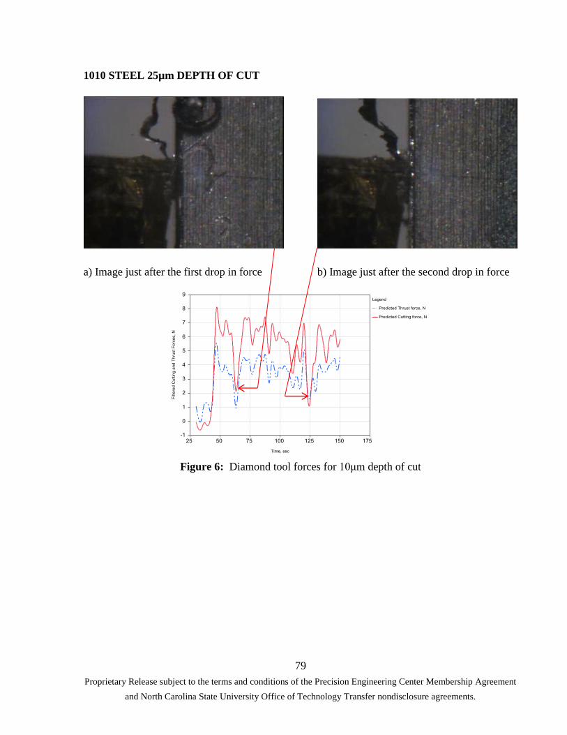
79
Proprietary Release subject to the terms and conditions of the Precision Engineering Center Membership Agreement
and North Carolina State University Office of Technology Transfer nondisclosure agreements.
1010 STEEL 25µm DEPTH OF CUT
a) Image just after the first drop in force b) Image just after the second drop in force
Figure 6: Diamond tool forces for 10μm depth of cut

80
Proprietary Release subject to the terms and conditions of the Precision Engineering Center Membership Agreement
and North Carolina State University Office of Technology Transfer nondisclosure agreements.
REFERENCES
1. AvantEdge created by ThirdWave Systems, Inc of Minneapolis, MN
2. A. Koplev, Aa. Lystrup, T. Vorm, The cutting process, chips, and cutting forces in machining
CFRP, Composites, Volume 14, Issue 4, October 1983, Pages 371-376.
3. Jiang Hua, Rajiv Shivpuri, Prediction of chip morphology and segmentation during the
machining of titanium alloys, Journal of Materials Processing Technology, Volume 150,
Issues 1-2, 1 July 2004, Pages 124-133.
4. A. Manna, B. Bhattacharyya, A study on machinability of Al/SiC-MMC, Journal of
Materials Processing Technology, Volume 140, Issues 1-3, Proceedings of the 6th Asia
Pacific Conference on materials Processing, 22 September 2003, Pages 711-716.

81
Proprietary Release subject to the terms and conditions of the Precision Engineering Center Membership Agreement
and North Carolina State University Office of Technology Transfer nondisclosure agreements.
8 ULTRASONIC VIBRATION ASSISTED MACHINING
Neil VonHolle
Undergraduate Student
Brandon Lane
Graduate Student
Thomas A. Dow
Professor, Mechanical and Aerospace Engineering
An ultrasonic elliptical vibration assisted machining (EVAM) device was designed and tested as
a summer undergraduate research project. This device utilized piezoelectric actuated resonator
called a sonotrode to oscillate a diamond tool. The resonant frequency and vibrational tool path
was determined using finite element modeling and the motion was corroborated using an
infrared displacement sensor. The vibrating tool was then used to cut 6061-T6 aluminum and
C360 brass. The resulting surface finish was poor possibly due to the compliant mounting of the
sonotrode base and metal pickup on the tool flank face may have been caused by errors in the
desired tool motion.
Workpiece Rotation
Diamond Tool
82
Proprietary Release subject to the terms and conditions of the Precision Engineering Center Membership Agreement
and North Carolina State University Office of Technology Transfer nondisclosure agreements.
8.1 INTRODUCTION
Elliptical vibration assisted machining, or EVAM, is the process where a tool is vibrated in two
orthogonal directions to create an elliptical path while machining a workpiece. The tool moves
in the direction of cutting as well as perpendicular to that direction which increases and reduces
the depth of cut. Because the tool can come out of contact with the workpiece, it is able to run
cooler but at the same time more sliding occurs than for conventional cutting. The reported
benefits of EVAM are decreased tool wear resulting in improved surface finish for longer cuts.
More details of the research activities in this subject are in Section 6 of this report.
The basic properties that define the motion of the EVAM process are the dimensions of the tool
ellipse, its frequency, the upfeed per cycle and the phase difference between the vibration
directions. The ellipse dimensions are defined as the amplitudes of vibration in the cutting
direction, a, and the vibration amplitude in the depth of cut direction, b. The upfeed is defined as
the horizontal distance the tool moves between consecutive cycles and can be found by dividing
the speed of cutting, V, by the frequency of vibration. The phase lag between the different
vibration directions dictates the tilt angle of the ellipse where 90o creates an ellipse with
amplitudes aligned with the x and z axis.
8.2 SONOTRODE
A sonotrode is an actuator driven at a ultrasonic frequency and includes a horn that amplifies this
vibratory energy to perform some activity such as ultrasonic welding or cutting. For an
ultrasonic welding or cutting application, the sonotrode gives energy directly to the welding
contact area, with little diffraction that could damage surrounding electronic components. In the
vibration assisted machining application described here, the sonotrode consists of a large
diameter rod that is excited by a piezoelectric actuator. Attached to the end of that rod a section
of decreasing cross sectional area whose length is related to the natural frequency of the driver.
When the large end of a sonotrode is excited at its natural frequency, the amplitude of the small
is amplified as the cross sectional area decreases. The shape and configuration of the sonotrode
dictates the amount of amplification. The sonotrode used in this project was designed with an
exponentially decreasing diameter from 48mm down to 12mm. It was machined to have a
mounting flange at the theoretical node of vibration. A NTK D4427 PZT piezoelectric actuator
is shown attached to the sonotrode in Figure 1. The actuator was sandwiched between sonotrode
and an additional mass with a preload applied by a bolt. The driver is called a BLT or a Bolted
Langvin Transducer.

83
Proprietary Release subject to the terms and conditions of the Precision Engineering Center Membership Agreement
and North Carolina State University Office of Technology Transfer nondisclosure agreements.
Figure 1. Sonotrode and FEA model
8.2.1 FE MODEL
A solid model of the sonotrode was created in SolidWorks and analyzed using the FE model,
Cosmos. The natural frequency for longitudinal vibration predicted by the FEA software was
24,906 Hz. The node, or point at which the vibration amplitude equals zero, was located in the
same place as the mounting flange on the sonotrode horn. The finite element displacement
results are shown in Figure 1.
Figure 2. Model of the sonotrode at the piezoelectric actuator (left) and at the end of the
reduced section (right)
Figure 2 shows the predicted amplitude of the sonotrode in the X direction from the FEM with a
sinusoidal excitation force at its resonant frequency of 10 N. The left image is the displacement
of the base or point of excitation and the right image is the amplitude at the small end. Both
graphs are on the same scale to emphasize the 2.6x magnification of the vibration amplitude.

84
Proprietary Release subject to the terms and conditions of the Precision Engineering Center Membership Agreement
and North Carolina State University Office of Technology Transfer nondisclosure agreements.
The phase difference between the point of excitation and the small end is 180o meaning that as
the actuator moves to the right, the small end is moving to the left.
8.2.2 SONOTRODE VIBRATION ANALYSIS
To create both X and Z motion, an off-center mass in the form of a tool and tool holder was
placed at the end of the tapered sonotrode. The actuator was excited using a function generator
with a 3V output signal and an amplifier was used to magnify the voltage by 100x. The actuator
excites the sonotrode at its natural frequency which vibrates the tool in the X direction. The off-
center mass of the tool creates a moment at the end of the beam that adds the orthogonal Z
motion. An optical sensor was used to measure the motion of the tool in the cutting (X) and
depth of cut (Z) directions. The oscilloscope is used to record the input signal from the function
generator as well as the output signal from the sensor.
The optical sensor is a light-based displacement sensor developed by Opto Acoustic Sensors that
can be used to measure small displacements at frequencies up to 50 KHz. It works by sending
near infrared light through a center emitting optical fiber and collecting the light reflecting off
the surface by six optical fibers surrounding the emitter. The amount of light received depends
on the standoff distance and this light is carried back by the receiving fibers to a photosensor and
is converted to an output voltage proportional to the distance to the target.
a) X direction motion at 27.5 KHz b) Z direction motion
c) Elliptical motion of the tool defined from X and Z motion in a) and b).
Figure 3. X and Z motion of the tool and the combined elliptical path at 27.5 KHz
Input waveform Input waveform
X displacement Z displacement

85
Proprietary Release subject to the terms and conditions of the Precision Engineering Center Membership Agreement
and North Carolina State University Office of Technology Transfer nondisclosure agreements.
To determine the shape of the tool motion, two measurements were made of this motion in the X
and Z directions; that is, the cutting direction and the direction of the depth of cut, respectively as
shown in Figure 3. By measuring the motion in each direction, the tool path can be estimated
based on the amplitude of the vibrations and the phase between them. Because the sensor had a
single channel, each motion was measured separately and compared to the input signal to the
amplifier for a phase measurement. Figure 3 shows the vibration of the tool at 27.5 kHz with a
10.1µm X amplitude, 3.23µm Z amplitude, and a 94o phase difference. Assuming sinusoidal
vibrations, the tool motion at 27.5 kHz was plotted to approximate the elliptical vibration shape
at the bottom of Figure 3. Sufficient detail was not necessarily available to know that they were
pure sine waves and thus the elliptical shape of the tool motion is somewhat idealized.
8.3 CUTTING EXPERIMENTS AND RESULTS
Due to the size of the sonotrode tool and the limited amount of space on the Diamond Turning
Machine (DTM), the optimum position of the sonotrode is shown in Figure 4. The actuator was
mounted horizontally and parallel to the face of the spindle. The large amplitude of the vibration
in Figure 3 will be in the direction of cutting and the smaller vibration will move the tool away
from the workpiece. The workpiece was a thin tube with a wall thickness approximately half the
thickness of the straight edge of the diamond tool. Figure 4 shows a solid model of this
apparatus illustrating the tool, sonotrode, and workpiece mounted on the diamond turning
machine as well as a photograph of the system.
Figure 4. Solid model of the machining experiment and the actual setup on the DTM
For the cutting experiments, the cutting velocity was chosen as 50 mm/s with a 5 µm depth of
cut. The system operated at 27.5 KHz frequency with the ellipse dimension shown in Figure 3.
The cutting parameters are 1.8 µm upfeed per cycle, maximum chip thickness of 1.2 µm and a
theoretical surface finish of 23 nm. To achieve these parameters, the DTM spindle rotated at

86
Proprietary Release subject to the terms and conditions of the Precision Engineering Center Membership Agreement
and North Carolina State University Office of Technology Transfer nondisclosure agreements.
0.716 revolutions per second. This is too slow for the main motor so an auxiliary stepper motor
was attached to the spindle to provide torque to handle the low turning speed.
Figure 5. SWLI image of brass surface with features at the upfeed rate of the actuator
For the EVAM testing, two materials were machined; 6061-T6 Aluminum and C360 Brass. A
white-light interferometer image of the brass substrate is shown in Figure 5. The main image
shows the overall machined surface and the right hand image is a slice from this image marked
in the lower left. The expected feature period of 1.8 mm is visible but many other features are
also present with magnitudes that were much larger than expected.
8.4 TOOL HOLDER COMPARISON
To explain the magnitude of the surface features, the influence of the tool holder stiffness was
evaluated. A pulley system was used to apply 1, 2 and 5 N forces to the tool in the cutting
direction and the depth of cut direction. Both the deflection of the sonotrode tool and a standard
diamond tool holder was measured. Figure 6 shows the deflection measured for each tool
support and the slope of these lines are reported in Table 1.
Table 1. Stiffness for the Sonotrode and Standard tool holder.
Tool Holder Stiffness, N/μm
Sonotrode Tool X direction 1.5
Sonotrode Tool Z direction 2.7
Standard Tool X direction 5.3
Standard Tool Z direction 8.0
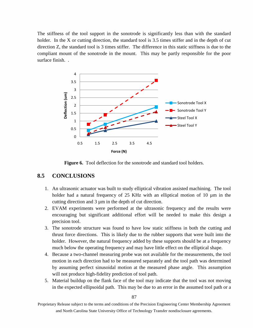
87
Proprietary Release subject to the terms and conditions of the Precision Engineering Center Membership Agreement
and North Carolina State University Office of Technology Transfer nondisclosure agreements.
The stiffness of the tool support in the sonotrode is significantly less than with the standard
holder. In the X or cutting direction, the standard tool is 3.5 times stiffer and in the depth of cut
direction Z, the standard tool is 3 times stiffer. The difference in this static stiffness is due to the
compliant mount of the sonotrode in the mount. This may be partly responsible for the poor
surface finish. .
Figure 6. Tool deflection for the sonotrode and standard tool holders.
8.5 CONCLUSIONS
1. An ultrasonic actuator was built to study elliptical vibration assisted machining. The tool
holder had a natural frequency of 25 KHz with an elliptical motion of 10 µm in the
cutting direction and 3 µm in the depth of cut direction.
2. EVAM experiments were performed at the ultrasonic frequency and the results were
encouraging but significant additional effort will be needed to make this design a
precision tool.
3. The sonotrode structure was found to have low static stiffness in both the cutting and
thrust force directions. This is likely due to the rubber supports that were built into the
holder. However, the natural frequency added by these supports should be at a frequency
much below the operating frequency and may have little effect on the elliptical shape.
4. Because a two-channel measuring probe was not available for the measurements, the tool
motion in each direction had to be measured separately and the tool path was determined
by assuming perfect sinusoidal motion at the measured phase angle. This assumption
will not produce high-fidelity prediction of tool path.
5. Material buildup on the flank face of the tool may indicate that the tool was not moving
in the expected ellipsoidal path. This may be due to an error in the assumed tool path or a
0
0.5
1
1.5
2
2.5
3
3.5
4
0.5 1.5 2.5 3.5 4.5
De
fle
ctio
n (
um
)
Force (N)
Sonotrode Tool X
Sonotrode Tool Y
Steel Tool X
Steel Tool Y

88
Proprietary Release subject to the terms and conditions of the Precision Engineering Center Membership Agreement
and North Carolina State University Office of Technology Transfer nondisclosure agreements.
phase error in the direction of the tool motion with respect to the workpiece motion. If
the tool was rotating in the wrong direction, the effect would be to have the tool “indent”
the workpiece as opposed to “scooping out” the chips. If the latter hypothesis was true, it
may be the cause of the tool pickup and poor surface finish.

89
Proprietary Release subject to the terms and conditions of the Precision Engineering Center Membership Agreement
and North Carolina State University Office of Technology Transfer nondisclosure agreements.
9 NANOCOINING OF OPTICAL FEATURES
Erik Zdanowicz
Graduate Student
Dr. Thomas A Dow
Duncan Distinguished University Professor
Department of Mechanical and Aerospace Engineering
Dr. Ronald Scattergood
Professor, Department of Material Science and Engineering
The use of non-reflective surfaces in consumer and commercial manufacturing has become
increasingly popular. Whether they are used to reduce reflection on a monitor or increase the
efficiency of photovoltaic solar cells, the advantages are being recognized and the demand is
increasing. The limitation of these non-reflective surfaces is the length of time required to
produce a useable quantity, usually by deposition techniques. This paper describes an approach
to creating non-reflective optical features with a high throughput.
The goal of this research is to create non-reflective surfaces through a process of nanocoining.
Nanocoining using a nanostructured diamond die to imprint the non-reflective structure on to a
mold surface. This type of manufacturing requires the design of an ultrasonic actuator (50 kHz)
to produce the indentations at a high rate. The physical process of the nano-indentation is
investigated to understand how material behaves at the nano-scale. A functional system will be
produced by creating experimental indents and comparing them to FEA results while
simultaneously designing a resonant structure capable of achieving the required displacements
at ultrasonic speeds. The ultrasonic actuator along with the ability to create nanostructured
features are the key elements to producing optical quality non-reflective surfaces efficiently.

90
Proprietary Release subject to the terms and conditions of the Precision Engineering Center Membership Agreement
and North Carolina State University Office of Technology Transfer nondisclosure agreements.
9.1 INTRODUCTION
The use of bio-inspired moth eye structures to decrease reflectivity of a surface has been
achieved with a variety of feature shapes, sizes, and orientations. In order to define the surface
that will be created by the nanocoining process, it is important to understand how these
parameters interact to create an antireflective surface. Through the study of naturally occurring
nano-features in certain insects, and the optical modeling of moth eye features, both naturally
occurring and man-made, it is possible to define the desired coined surface for antireflection.
This paper will review the optical theory and resulting constraints required for reduced
reflectivity on the nanocoined surface.
9.1.1 BIO-INSPIRED OPTICAL FEATURES
The model for the features that will be created by the nanocoining process comes from the
naturally occurring features present in the eyes of some insect species. These features, known as
corneal nipples, are commonly found in nocturnal moths and diurnal butterflies. Corneal nipples
are protuberances on the outer surface of the eye that have been found in a variety of shapes and
sizes. They are typically hexagonally arrayed, but similar to grain orientation in materials, the
orientation of the features is not perfectly consistent across the surface. Figure 1 shows the
features and orientation shifts found on a typical moth eye surface [1].
Figure 1. Corneal Nipple Array of Peacock Butterfly SEM image (Scale bar is 2 micrometers)
[1]

91
Proprietary Release subject to the terms and conditions of the Precision Engineering Center Membership Agreement
and North Carolina State University Office of Technology Transfer nondisclosure agreements.
Corneal nipples are usually found with maximum heights, h, around 250nm. The spacing
between features, d, is generally between 175nm and 250nm. Stavenga [1] published
simulations showing different feature profiles and heights, and the impact on reflectivity over the
wavelength, λ, range of visible light, 300 – 700nm.
This study uses the theory that the moth eye features create an optical layer where the ratio of
material to air varies with distance from the top of the features to the base of the features. This
ratio of air to material is directly related to the index of refraction. As a result, the index of
refraction changes over the optical layer from that of air, 1, to that of the substrate material
gradually through the optical layer [2]. This can be modeled based on the geometry of the
features and the spacing of the features by taking the optical surface and dissecting it into many
sublayers. An average index of refraction can be calculated for each sublayer and then the
optical surface can be treated as stacked layers of thin film. Figure 2 shows how the optical
surface can be divided into these sublayers.
Figure 2. Cross section of optical layer dissected into thin sublayers for analysis
This analysis shows that taller features reduce reflectivity in moth eyes from around 4% (for 50
nm tall features) to less than 1% (for 250 nm tall features) across the entire visible light spectrum
for all feature shapes examined [1].
Another study performed by Hutley and Wilson describes the dimension requirements of the
optical layer for reduced reflectivity [2]. Theoretically, since each sublayer has a different index
of refraction, the reflected light has a different phase at each depth. If the height of the optical

92
Proprietary Release subject to the terms and conditions of the Precision Engineering Center Membership Agreement
and North Carolina State University Office of Technology Transfer nondisclosure agreements.
layer is at least half the size of the wavelength of the incident light, then all phases occur and
destructive interference causes the reflectivity to drop to zero. The geometry of the feature,
parabolic, cone, pyramidal or Gaussian profile, does contribute to this effect, but the minimum
reflectance consistently occurs when the feature height is close to half the wavelength of the
incident light [1]. This is shown in Equation (1).
(1)
The feature spacing has a direct effect on diffusion of incident light at normal and oblique
incidence. If the array is too widely spaced, then the optical layer will act as a diffraction
grating. If the spacing, d, is small enough then the reflectivity will be minimized and the
transmissivity maximized. Equation (2) describes how the wavelength of incident light, λ, and
index of refraction of the substrate, n, affect the feature spacing, d.
(2)
Using this theory, the parameters for the target nanocoined surface are defined. The goal of this
project is to make an antireflective moth eye surface for incident light in the visible spectrum.
The minimum wavelength to be transmitted, λmin, is 380 nm. The maximum wavelength to be
transmitted, λmax, is 780 nm. As a result the features in the optical layer should have a target
height, h, of 390 nm and target feature spacing, d, of 190 nm.
9.2 DETAILS OF THE PROJECT
There are many considerations to account for to reach a functional system. Material effects such
as strain rate and grain size must be discussed. Creating nano-featured indents and comparing
the results to FEA simulations will provide a method to predict forces and material
displacements caused by dies with different geometries. The indentation process itself is a
challenging task. The die must imprint on a moving surface which means unless some kind of
compensation is implemented, the imprints could smear. To avoid smear the actuator must not
only be ultrasonic, but produce displacements in more than one direction. This is a very difficult
task considering the required displacements of the die. These challenges have all been diligently
addressed and the results will be discussed in the following sections.

93
Proprietary Release subject to the terms and conditions of the Precision Engineering Center Membership Agreement
and North Carolina State University Office of Technology Transfer nondisclosure agreements.
9.2.1 EFFECT OF STRAIN RATE ON HARDNESS IN NANOCOINING
The rate of the die indentation proposed for nanocoining is on the order of 40 kHz. This means
that the effective strain rate for making an indentation would be very high compared to
conventional indentation testing. An estimate of the rate effect is appropriate to see if the rate has
a large influence on the indentation forces. If it does, this would have to be taken into account in
the design of the die actuator.
For spherical indentation the hardness H is related to the yield stress by the by the constraint
factor c
(3)
c ≈ 3 when the plastic zone fully encloses the indenter up to the free surface. It is between 1 and
3 when the plastic zone is constrained to the subsurface [2].
The strain rate effect in uniaxial tension or compression relates the yield stress to the strain rate
d/dt =
(4)
The constant A and the strain rate sensitivity m depend on the material and its condition (alloy
content, cold working, grain size, etc.). An effective uniaxial indentation strain for spherical
indentation is given by the ratio of the diameter d of the indentation projected on the free surface
to the diameter D of the indenter [2]. For a fixed value of = d/D in nanocoining, the effective
indentation strain rate would then be
(5)
∆t is the mean time needed to produce an indent, which is 1/ where is the nanocoining
frequency. Combining these relations and assuming that the constraint factor c is a constant
independent of indentation rate,
(6)
The subscript “o” denotes values for a conventional hardness test with respect to values for
nanocoining. Taking vo = 1 s-1
and v = 40000 s-1
for a comparison, ie., nanocoining at 40 kHz,
the relative strain rate induced hardness increase for nanocoining would be (40000)m where m is
the strain rate sensitivity in uniaxial compression or tension.

94
Proprietary Release subject to the terms and conditions of the Precision Engineering Center Membership Agreement
and North Carolina State University Office of Technology Transfer nondisclosure agreements.
As a simple approximation of the material response, the value of m for large grain size pure
copper is about 0.005 (grain size on the order of 10 to 20 µm or larger). The value of m increases
with decreasing grain size and m would be about 0.015 for nano grain size copper, for example,
electroplate copper. Using these values, the ratio H/Ho would increase from about 1.05 to 1.15 as
the grain size of Cu decreases to the nanoscale. At the largest m value considered, this is only a
15% increase in hardness for nanocoining. This would not have a significant impact on the
indentation forces during a nanocoining operation.
Figure 3 shows experimental data for compression tests on 150 nm grain size pure copper. The
tests at the lower strain rates (solid points) were obtained from uniaxial compression tests and the
values at higher strain rates (open points) were obtained using the Hopkinson split bar technique
[4]. A yield stress increase of about 33% is obtained at the highest-to-lowest strain rate ratio of
1.1 x 10⁷. This is consistent with an average m value of 0.0176 for the copper, in agreement with
the approximate analysis presented in this section.
Figure 3. Compression tests (filled data points) and Hopkinson bar test (open data points) for
tests done at 293 K on pure copper with an average grain size of 150 nm [4].
9.2.2 EXPERIMENTAL INDENTATIONS
Real indents were created for comparison with an FEA model. The goal is to have confidence
that a die producing indents with attractive material deformation can be designed using FEA
software (ANSYS). This is essential since the dies are constructed by use of Focused Ion Beam
(FIB) machining diamond blanks. As a first step, a Rockwell indenter was used.

95
Proprietary Release subject to the terms and conditions of the Precision Engineering Center Membership Agreement
and North Carolina State University Office of Technology Transfer nondisclosure agreements.
Rockwell Indenter Tests
A Rockwell indenter was chosen as a starting point because of they are inexpensive, readily
available and have a simple geometry. Although a Rockwell indenter may look like a cone, there
is a 200 µm radius spherical tip. It is this part of the geometry that was used for the experiments
and models. Using only the spherical tip of the Rockwell indenter (limited by force) several
indents were made on a sample of 6061 Al.
A displacement based model was created in ANSYS to compare load vs. indention depth. This
implies that the indenter geometry was displaced a certain amount and the resulting forces from
the contacting faces were calculated. This process was repeated until a certain depth was
reached, after which the indenter was removed from the material leaving a plastically deformed
indent. A bilinear isotropic material model was used to capture the effects of plasticity and strain
hardening. The model which exploits the symmetry of the geometry can be seen in Figure 4.
Figure 4. ANSYS simulation results of indentation using spherical portion of a Rockwell
hardness indenter.
The experimental indents were measured with the Zygo Scanning White Light Interferometer
(SWLI) and the results compared with the FEA simulations can be seen in Table 1.
Table 1. Results of Rockwell indents and FEA simulation.
Mass
(kg)
ANSYS
(μm)
Experimental
(μm)
0.2 1.5 1.4
0.4 2.8 2.9
0.52 3.4 3.2
0.62 3.6 3.9

96
Proprietary Release subject to the terms and conditions of the Precision Engineering Center Membership Agreement
and North Carolina State University Office of Technology Transfer nondisclosure agreements.
Table 1 shows that, for the Rockwell indenter, the ANSYS model correlates well. The next step
was to scale down to a more applicable indenter size.
3M Flat Die Indents
The next set of indents was created using a diamond die with a 100 x 100 µm flat, square face.
This tool was essentially a blank and provided for practice before using a nanostructured die
which has time and effort invested. A rendering of the tool and tool holder can be seen in Figure
5.
Figure 5. Flat diamond die and holder provided by 3M.
Indents would be created using the Nanoform 4-axis precision machine. The Nanoform has 3
translational axes (x, y, and z) and a rotational axis (not used for indents). An electroplated
copper sample was used as a work-piece because of the small grain size. The work-piece was
mounted to a block fixed to the x-axis. A load cell was placed between the work-piece and
mounting block so indentation forces could be measured. The diamond tool was then attached to
the y-axis tower of the Nanoform. The y-axis tower resides on the z-axis of the Nanoform. The
z-axis was used to move the die into the work-piece and the x and y axes where used to move the
die to a new indentation position. Figure 6 shows the experimental setup on the Nanoform.
Figure 6. Experimental indentation setup on Nanoform (left) and alignment fixture (right).
Figure 6 also shows an alignment fixture that allows rotational adjustments of the die. This
feature is required to ensure the flat face of the die is parallel to the flat work-piece face. If the
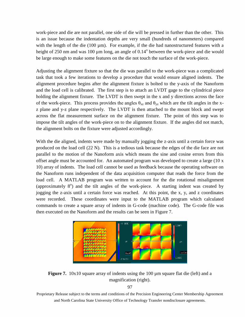
97
Proprietary Release subject to the terms and conditions of the Precision Engineering Center Membership Agreement
and North Carolina State University Office of Technology Transfer nondisclosure agreements.
work-piece and die are not parallel, one side of die will be pressed in further than the other. This
is an issue because the indentation depths are very small (hundreds of nanometers) compared
with the length of the die (100 µm). For example, if the die had nanostructured features with a
height of 250 nm and was 100 µm long, an angle of 0.14o between the work-piece and die would
be large enough to make some features on the die not touch the surface of the work-piece.
Adjusting the alignment fixture so that the die was parallel to the work-piece was a complicated
task that took a few iterations to develop a procedure that would ensure aligned indents. The
alignment procedure begins after the alignment fixture is bolted to the y-axis of the Nanoform
and the load cell is calibrated. The first step is to attach an LVDT gage to the cylindrical piece
holding the alignment fixture. The LVDT is then swept in the x and y directions across the face
of the work-piece. This process provides the angles θxz and θyz which are the tilt angles in the x-
z plane and y-z plane respectively. The LVDT is then attached to the mount block and swept
across the flat measurement surface on the alignment fixture. The point of this step was to
impose the tilt angles of the work-piece on to the alignment fixture. If the angles did not match,
the alignment bolts on the fixture were adjusted accordingly.
With the die aligned, indents were made by manually jogging the z-axis until a certain force was
produced on the load cell (22 N). This is a tedious task because the edges of the die face are not
parallel to the motion of the Nanoform axis which means the sine and cosine errors from this
offset angle must be accounted for. An automated program was developed to create a large (10 x
10) array of indents. The load cell cannot be used as feedback because the operating software on
the Nanoform runs independent of the data acquisition computer that reads the force from the
load cell. A MATLAB program was written to account for the die rotational misalignment
(approximately 8o) and the tilt angles of the work-piece. A starting indent was created by
jogging the z-axis until a certain force was reached. At this point, the x, y, and z coordinates
were recorded. These coordinates were input to the MATLAB program which calculated
commands to create a square array of indents in G-code (machine code). The G-code file was
then executed on the Nanoform and the results can be seen in Figure 7.
Figure 7. 10x10 square array of indents using the 100 µm square flat die (left) and a
magnification (right).

98
Proprietary Release subject to the terms and conditions of the Precision Engineering Center Membership Agreement
and North Carolina State University Office of Technology Transfer nondisclosure agreements.
The 1mm square block of 100 indents is aligned well in the plane of the page but there is a tilt of
the die relative to the work-piece. It should be noted that this block was created before the final
alignment procedure was developed. An unexpected feature observed upon measurement of the
indents is that there was a significantly larger amount of plastic deformation around the edge of
the indents. This additional plastic deformation can be seen in Figure 8 which is a trace of the
right hand image in Figure 7. The additional edge deformation is from the stress concentration
caused by the sharp corner at the edge of the die. This will be discussed more in the
nanostructured die indents section.
Figure 8. Trace of right measurement in Figure 7 depicting additional deformation at edge of
indent.
3M Nanostructured Die Indents
The experience gained from the experiments with the flat die provided confidence that indents
could be made using a nanostructured die. Once again, 3M provided the diamond die, this time
with features created on the face using a Focused Ion Beam (FIB). Scanning Electron
Microscope (SEM) images of the die are shown in Figure 9.
Figure 9. SEM images of nanostructured die provided by 3M Corporation.

99
Proprietary Release subject to the terms and conditions of the Precision Engineering Center Membership Agreement
and North Carolina State University Office of Technology Transfer nondisclosure agreements.
The left image in Figure 9 shows a closer, slightly tilted view of the nanostructured die. The die
consists of a square inner region containing a 40x40 array of square features. Each feature is
approximately 300 x 300 nm in cross section and 250 nm in height. Spacing between features is
200 nm. The right image in Figure 9 is orthogonal to the die face and shows a square boarder
around the inner region containing the nano-features. The outside dimensions of the boarder are
approximately 25x25 nm. The surface of this boarder is the same height as the tips of nano-
features and is used as an alignment indicator when measuring with the Zygo SWLI. The same
procedure used to create the array of flat indents was used to create an 11x10 array of
nanostructured indents. One of the indents in the array measured by an SEM can be seen at
different magnifications in Figure 10.
Figure 10. Single nanostructured indent measured with SEM at 5000x (left) and 10000x (right).
Figure 10 is an SEM image of a single indent in a corner of the array. The material above and to
the left of the boarder is a non-indented surface. The SEM images show the border and nano-
features clearly although depth dimensions cannot be determined. The most significant piece of
information the image provides is the presence of the additional plastic deformation at the edge.
This can be seen by examining the two scratches that cross each other in the left image of Figure
10. The scratches were present on the surface before the indent so it has been pushed down with
the rest of the surface. However the scratch seems to disappear at the edge of the border and un-
deformed material. This is because the material has been deformed more at this edge from the
sharp edge stress concentration. Fabrication of future dies will have to compensate for the
uneven contact stress created by flat dies. A way to compensate for this is discussed in the next
section.

100
Proprietary Release subject to the terms and conditions of the Precision Engineering Center Membership Agreement
and North Carolina State University Office of Technology Transfer nondisclosure agreements.
While SEM imaging is an effective way to measure 2-D features, the nanostructures are three
dimensional and all three dimensions are important when considering the criteria for a non-
reflective surface. A way to measure all three dimensions at once is by using an Atomic Force
Microscope (AFM). An AFM is essentially a nano-scale profilometer that rasters over an area of
a surface. Figure 11 is an AFM measurement of 1.5x1.5 µm patch located in the nanostructured
area of the indent shown in Figure 10.
Figure 11. AFM measurement of nanostructure features (left) and 3-D rendering (right).
The left image in Figure 11 is a profile trace across the pockets created by the nano-features on
the die. The data from the trace indicates that a depth of approximately 30 nm was reached.
This was far from the total height of the nano-features so future indents will have to be
performed to ensure the die has been indented to full depth.
9.2.3 FEA SIMULATIONS OF NANOSTRUCTURED DIE INDENTS
One of the goals of this research is to develop an accurate FEA model of the indentation process.
This will provide a better understanding of how the material will deform and what can be done to
influence material behavior. An example of material behavior that requires attention is the
additional plastic deformation observed at the edge of the indents. Before compensation
techniques can be applied a simulation must be developed to accurately model the
nanostructured die indents.
The FEA model was created in ANSYS using 2-D geometry for computational purposes. The
model takes advantage of geometrical symmetry so only half of the indenter and work-piece
were modeled. Material properties for diamond and electroplated copper were used for the
indenter and work-piece respectively. A bilinear isotropic material model which included strain
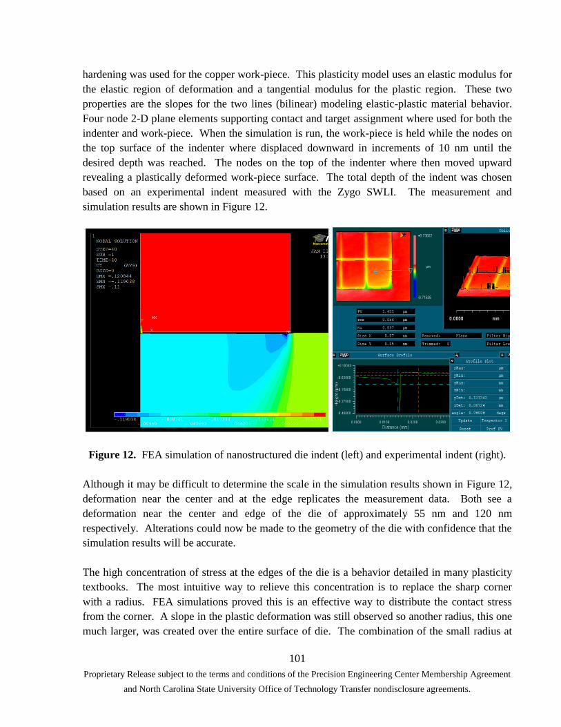
101
Proprietary Release subject to the terms and conditions of the Precision Engineering Center Membership Agreement
and North Carolina State University Office of Technology Transfer nondisclosure agreements.
hardening was used for the copper work-piece. This plasticity model uses an elastic modulus for
the elastic region of deformation and a tangential modulus for the plastic region. These two
properties are the slopes for the two lines (bilinear) modeling elastic-plastic material behavior.
Four node 2-D plane elements supporting contact and target assignment where used for both the
indenter and work-piece. When the simulation is run, the work-piece is held while the nodes on
the top surface of the indenter where displaced downward in increments of 10 nm until the
desired depth was reached. The nodes on the top of the indenter where then moved upward
revealing a plastically deformed work-piece surface. The total depth of the indent was chosen
based on an experimental indent measured with the Zygo SWLI. The measurement and
simulation results are shown in Figure 12.
Figure 12. FEA simulation of nanostructured die indent (left) and experimental indent (right).
Although it may be difficult to determine the scale in the simulation results shown in Figure 12,
deformation near the center and at the edge replicates the measurement data. Both see a
deformation near the center and edge of the die of approximately 55 nm and 120 nm
respectively. Alterations could now be made to the geometry of the die with confidence that the
simulation results will be accurate.
The high concentration of stress at the edges of the die is a behavior detailed in many plasticity
textbooks. The most intuitive way to relieve this concentration is to replace the sharp corner
with a radius. FEA simulations proved this is an effective way to distribute the contact stress
from the corner. A slope in the plastic deformation was still observed so another radius, this one
much larger, was created over the entire surface of die. The combination of the small radius at

102
Proprietary Release subject to the terms and conditions of the Precision Engineering Center Membership Agreement
and North Carolina State University Office of Technology Transfer nondisclosure agreements.
the edge and large radius over the entire face produced a nearly uniform contact pressure under
the face of the die as shown in Figure 13.
Figure 13. FEA displacement of multiple radii die (left), comparison of contact stress (right).
Figure 13 shows the results of the simulation run with a die that has two radii. The solution
method is the same as for the flat die but the results are much more uniform due to the near linear
contact stress across the face of the die. The top right image of Figure 13shows the contact stress
of the flat die. The stress near the center and edge are 606 MPa and 1412 MPa respectively. The
stress at the edge is more than twice the stress at the center. The contact stress of the die with
multiple radii (shown in lower right of Figure 13) has a maximum stress of 676 MPa. The
variation is not distinguishable because range of the color bar. This is evidence that altering the
face of the die by adding two radii will produce a more favorable indent. The FEA simulation
allowed this problem to be addressed by trying potential die shapes.
9.2.4 CHARACTERIZATION OF TOOL MOTION
The objective of this research is to develop an indentation system that will not only produce
features with optical fidelity but do so at a high rate. To accomplish this task the work-piece
must travel at a constant velocity. This implies that a die stroke orthogonal to the work-piece
will not work because of the difference in velocities between the die and work-piece at the time

103
Proprietary Release subject to the terms and conditions of the Precision Engineering Center Membership Agreement
and North Carolina State University Office of Technology Transfer nondisclosure agreements.
of contact (die not moving in direction of work-piece). A difference in velocities when there is
contact for some amount of time, Δt, will cause smear as shown in Figure 14 where VxDie is the
horizontal velocity of the die and VxWork-piece is the horizontal velocity of the work-piece.
Figure 14. Smear caused by orthogonal die actuation.
To accommodate for the velocity difference the die must travel in the x-direction to match speed
with the work-piece. The die must also be able to change direction and travel back to its origin
so there is no over-lap or gap between successive indentations. With these stipulations in mind
the ideal shape is an ellipse where the maximum velocity in the x-direction matches the work-
piece velocity. Figure 15 shows the die‟s velocity as it moves through one elliptical cycle.
Figure 15. Elliptical motion of die for one cycle.
The motion of the die along the path must be well choreographed with the speed of the work-
piece in order to minimize smear and produce equally spaced features. Therefore, relationships
between the die and work-piece‟s position and velocity must be established
A model of the die motion with respect to the work-piece was developed to gain an
understanding of which properties of the motion affect the overall performance. The x and y
positions of the die where modeled by
x
y

104
Proprietary Release subject to the terms and conditions of the Precision Engineering Center Membership Agreement
and North Carolina State University Office of Technology Transfer nondisclosure agreements.
(7)
(8)
where ω is the frequency of oscillation, t is time, a is the amplitude of the ellipse in the x-
direction and b is the amplitude of the ellipse in the y-direction (Figure 15). Equations 7 and 8
can be used to relate the position and velocities of the die and work-piece. The result is a model
with three defining variables which are the length of the die, frequency of indentation and
velocity of the work-piece. A change in any one of these variables will cause the other two to
change for a system were the indentations are sequentially aligned. Figure 16 shows a
simulation of the system as a function of the die length, frequency and work-piece velocity.
Figure 16. Simulation of elliptical path while indenting work-piece moving at constant velocity.
The different color line segments of the work-piece in Figure 16 represent successive
indentations (which equal the length of the die). When the simulation is run at speed, the red box
(die) will contact the work-piece at each line segment, one per cycle, meaning no overlap or
gaps. The simulation also implies that the dimension, a, is fixed for a given die geometry and
frequency. The dimension, b, is free to be adjusted which will be seen when error is examined.
Future work includes developing and actuator that is capable of producing the desired elliptical
shape.

105
Proprietary Release subject to the terms and conditions of the Precision Engineering Center Membership Agreement
and North Carolina State University Office of Technology Transfer nondisclosure agreements.
Smear Error Relationship between Ellipse Dimensions
Figure 16 shows a „long‟ tool path which implies the „a‟ dimension of the ellipse is larger than
the „b‟ dimension (if a = b then the path is a circle). Even though the tool is moving in an
elliptical path there will still be some amount of smear since the die will come into contact with
the work-piece before the die reaches its maximum x-direction velocity (refer to Figure 15 for
variable definitions). Initially it was assumed that the long ellipse would be the best tool path
shape. Error analysis was performed by simply calculating the difference in die and work-piece
velocity when the two are in contact. This error analysis was performed for different dimensions
of b since a is a fixed dimension. The results showed that a „tall‟ ellipse (where the b dimension
is larger than the a dimension) produces less error than the long elliptical tool path. This
property can be easily understood if the x-velocity and total cycle time are considered in Figure
15. The x-velocity in the long ellipse takes longer to reach maximum velocity (work-piece
velocity) than a tall ellipse. This implies that for a tall ellipse, the die accelerates faster and is in
contact less amount of time than the long ellipse. The relationship on how the b dimension
influences the error is shown in Figure 17.
Figure 17. Smear error (nm) vs. the vertical ellipse dimension, b.
Figure 17 shows that as the b dimension increases, the error decreases. The b dimension cannot
be very large however since these amplitudes are difficult to achieve at a 50 kHz actuation
frequency. Therefore, vertical amplitude of 8 µm was chosen for 4.77 µm horizontal amplitude.
To achieve these large amplitudes (relative to operating frequency) in two directions, an
ultrasonic actuator has to be designed that can generate this motion without tilting the die and
creating misalignment.

106
Proprietary Release subject to the terms and conditions of the Precision Engineering Center Membership Agreement
and North Carolina State University Office of Technology Transfer nondisclosure agreements.
9.3.5 ULTRASONIC ACTUATOR DESIGN
The actuator for the nanocoining process must operate at 50 kHz and produce motion in two
directions. The choice of actuator types is limited at such high frequencies so an ultrasonic
resonant piezoelectric actuator was selected. This type of actuator uses piezoelectric material
(PZT) to vibrate a structure at its resonant frequency. PZT material has a very high bandwidth
and operating at resonance will produce amplification in displacement that is required by the
specified tool path. After developing different models and simulating their response to a PZT
actuation, a challenge arose in every design. The challenge is how to keep the die from rotating
during actuation. Referring to Figure 15, the desired motion of the tool is rigid body translation
in two directions. Any type of rigid body rotation of the die could generate misaligned indents.
The initial actuators were designed to use two mode shapes to generate the motion amplification
in two directions. These mode shapes were a longitudinal and bending. The first design (Figure
18) is a combination of three ultrasonic horns connected at a center tool holder.
Figure 18. Three ultrasonic horn actuator design and response.
The ultrasonic horn shown in Figure 18 is a type of mechanical amplifier used to achieve large
displacements. The amplification is a function in the change in radius from the base to the tip.
The right image of Figure 18 shows the harmonic response to a sine wave at 50 kHz. This
actuator will generate the desired displacements although there is some tilt when the actuator is
not in the indentation part of its cycle. The indent would have to take place precisely at the right
point to have an acceptable result. This actuator will produce the displacement necessary for the
required indents but because of the additional rotation, other options will be considered.
Another design for the ultrasonic actuator was inspired by former Precision Engineering Center
student Markus Bauer. Bauer created an actuator out of a solid piece of piezoelectric material.
By poling the material correctly and placing electrodes (locations of actuation) at correct

107
Proprietary Release subject to the terms and conditions of the Precision Engineering Center Membership Agreement
and North Carolina State University Office of Technology Transfer nondisclosure agreements.
positions, he was able to actuate the structure at a longitudinal and bending mode
simultaneously. Using the same concept, an actuator for the nanocoining application was
designed by first starting with a beam with fixed supports at each end. The dimensions of the
beam were chosen based on the material properties and desired frequencies. The model shown
in Figure 19 was the result.
Figure 19. Model and simulation response of resonant PZT beam actuator.
The beam is modeled as if two PZT layers were epoxied together. An electrode runs down the
center of the beam and functions as a ground. Six electrodes, three on the top and three on the
bottom, are placed on the outside of the beam. The center of the beam can then be actuated in an
elliptical path by applying voltages at these electrodes and varying the phase. The disadvantage
of this approach is that the displacements are too small. The advantage of the beam is that its
frequencies are well characterized and this feature was used to develop another concept.
The previous model used a longitudinal and bending mode of a beam with fixed ends to produce
elliptical motion. A variation on this design uses a beam with a square cross section fixed at
both ends. The length and cross section were chosen so the first bending mode was at 50 kHz.
Since the cross section is square there are two bending modes at 50 kHz whose directions of
displacement are orthogonal. Actuating the beam in both directions causes the center of the
beam to move in an elliptical path.
A source of actuation that has been researched is through a Bolted Langevian Transducer (BLT).
A BLT is composed of two masses with PZT material between them. A bolt is then used to
clamp the two masses together compressing the PZT material. The resulting structure is in
essence a spring-mass system whose natural frequency is based on the masses and bolt/PZT
material. An image of a BLT can be seen in Figure 20.

108
Proprietary Release subject to the terms and conditions of the Precision Engineering Center Membership Agreement
and North Carolina State University Office of Technology Transfer nondisclosure agreements.
Figure 20. Image of BLT. Two aluminum masses bolted together with PZT material between.
A BLT such as the one shown in Figure 20 can be used to actuate the beam with 50 kHz resonant
frequency. There has to be an interface/fixture connecting the beam to the BLT which supports
the beam as specified in the model and remains stiff enough not to add additional modal
influences. The system shown in Figure 21 was designed so that the beam is embedded in the
end of the fixture. This fixture is then bolted to the BLT and the entire assembly is supported by
a flange. The flange is located at one of the nodes of the 50 kHz mode shapes so as not to
influence the dynamics.
Figure 21. BLT with beam fixture attached and support flange at node location.
The actuation of the assembly in Figure 21 has not yet been fully designed as most BLTs are
actuated in one direction. However, it is known that BLTs have been created with PZT material
poled off axis. Actuating these types of PZT rings generate motion in two directions which is
required for the nanocoining application. Further investigation into these PZT rings is ongoing.
9.3 CONCLUSIONS
The creation of non-reflective surfaces with high fidelity features at a rapid rate is emerging area
of research. These non-reflective sheets have a variety of applications and the ability to produce
109
Proprietary Release subject to the terms and conditions of the Precision Engineering Center Membership Agreement
and North Carolina State University Office of Technology Transfer nondisclosure agreements.
them in mass quantities will broaden their use. Nanocoining non-reflective surfaces are an
alternative method to the deposition techniques that are currently being used. Nanocoining
surfaces are possible by using a ultrasonic 50 kHz resonant actuator to indent a diamond die into
a mold material. Experiments have shown that indenting nano-features into a copper work-
piece is possible and an experimental procedure for aligning the indents has been established.
FEA models have been developed that accurately model the experimental indents and will be
used to optimize the die geometry for uniform indents. FEA is also being used to simulate how
different actuator designs perform at resonance. Future research includes examining how
subsequent indents affect each other as well as how to produce desired motion from the actuator
designs.
REFERENCES
1. Stavenga, G. C., S. Foletti, G. Palasantzas and K. Arikawa, Light on the Moth-Eye Corneal
Nipple Array of Butterflies, Proceedings of the Royal Society B, vol. 273 no. 1587, 661-667,
(2006).
2. Wilson, S. J. and M. C. Hutley, Optical Properties of ‘Moth Eye’ Antireflection Surfaces,
Journal of Modern Optics, 29:7, 993-1009, (1982).
3. Johnson K L, “Contact Mechanics”, Cambridge University Press 1985.
4. Tau S, Yu-Long L, Kui X, Feng Z, Ke-Shi Z, Qiong D, “Experimental investigation on
strain rate sensitivity of ultra-fine grained copper at elevated temperatures”, submitted to
Mech. of Matls. 2010.

Proprietary Release subject to the terms and conditions of the Precision Engineering Center Membership Agreement
and North Carolina State University Office of Technology Transfer nondisclosure agreements.
111
FACULTY
THOMAS A. DOW
Director, Precision Engineering Center
Dean F. Duncan Distinguished University Professor in Mechanical Engineering
Professor, Department of Mechanical and Aerospace Engineering
BS, Mechanical Engineering, Virginia Polytechnical Institute, 1966
MS, Engineering Design, Case Institute of Technology, 1968
PhD, Mechanical Engineering, Northwestern University, 1972
After receiving his PhD degree from Northwestern University in 1972, Dr. Dow joined the
Tribology Section of Battelle Columbus Laboratories and worked there for ten years. His
research interests were in the areas of friction and wear and included studies on a wide variety of
topics from lubrication of cold-rolling mills using oil-in-water emulsions to wet braking
effectiveness of bicycle brakes to elastohydrodynamic lubricant film generation in ball and roller
bearings. He developed experimental apparatuses, established analytical models, and
corroborated those analyses with experimental measurements. Dr. Dow joined the faculty at
North Carolina State University in 1982 and was instrumental in developing the academic and
research program in precision engineering. His current research interests include the design of
precision machining systems, real-time control, and metrology. He was one of the founders of
the American Society for Precision Engineering and currently acts as the Executive Director.

Proprietary Release subject to the terms and conditions of the Precision Engineering Center Membership Agreement
and North Carolina State University Office of Technology Transfer nondisclosure agreements.
112
JEFFREY W. EISCHEN
Associate Professor
Department of Mechanical and Aerospace Engineering
BS, Mechanical Engineering, UCLA, 1978
MS, Mechanical Engineering, Stanford University, 1981
PhD, Mechanical Engineering, Stanford University, 1986
Dr. Eischen has been with North Carolina State University since 1986 and his research areas of
interest include: linear and nonlinear finite element analysis, multi-body
kinematics/dynamics/control, fabric mechanics, and stress analysis in microelectronic devices.
He teaches undergraduate courses in strength of mechanical components and mechanical design.
His graduate courses include fracture mechanics and advanced machine design. He has
collaborated with colleagues in the Precision Engineering Center for several years on computer
simulation related projects dealing with precision shape control of disk drive read/write heads,
stress and deformation analysis of high energy physics equipment, and contact lens mechanics.

Proprietary Release subject to the terms and conditions of the Precision Engineering Center Membership Agreement
and North Carolina State University Office of Technology Transfer nondisclosure agreements.
113
RONALD O. SCATTERGOOD
Professor
Materials Science and Engineering Department
BS, Metallurgical Engineering, Lehigh University, 1961
MS, Metallurgy, Massachusetts Institute of Technology, 1963
PhD, Metallurgy, Massachusetts Institute of Technology, 1968
R.O. Scattergood is a Professor in the Department of Materials Science and Engineering. He
received BS degrees in Mining Engineering and Metallurgical Engineering from Lehigh
University. His MS and PhD degrees were obtained in Metallurgy from M.I.T. In 1968 he
became a member of the basic research staff in the Materials Science Division at the Argonne
National Laboratory. In 1981, he joined the faculty as a Professor of Materials Engineering at
North Carolina State University.
Professor Scattergood's major research interests have been focused on the mechanical behavior of
solids. He has worked in the areas of strengthening mechanisms in solids, mechanical testing,
fracture, tribology, nanocrystaline materials and precision machining processes. He has
published over 200 technical papers, books and reports.

Proprietary Release subject to the terms and conditions of the Precision Engineering Center Membership Agreement
and North Carolina State University Office of Technology Transfer nondisclosure agreements.
114
STAFF
KENNETH P. GARRARD
Senior Research Associate
Precision Engineering Center
BS, Computer Science, North Carolina State University, 1979
MS, Computer Studies, North Carolina State University, 1983
As a full-time staff researcher at the Precision Engineering Center, Mr. Garrard's interests and
duties have included the development of high performance control systems for ultra-precision
machines and software development for custom, multiprocessor computer systems. He
participated in the development of the original PEC fast tool servo as well as three other fast tool
servo systems that have been delivered to commercial and government sponsors. One of these
systems was built specifically for the on-axis turning of off-axis segments of conic surfaces of
revolution and another is being used for the fabrication of inertial confinement fusion target
mandrels. He has performed numerous prototype fabrication projects that required unique
machine configurations and controller software. Mr. Garrard also has a long standing interest in
the analysis of scientific data, programming language structures, sorting and searching
algorithms, multiprocessor computer architecture and the design and implementation of hard
real-time systems.

Proprietary Release subject to the terms and conditions of the Precision Engineering Center Membership Agreement
and North Carolina State University Office of Technology Transfer nondisclosure agreements.
115
ALEXANDER SOHN
Research Assistant/Lecturer
Precision Engineering Center
B.S., Physics, University of Texas at Arlington, 1992
M.S., Physics, University of Texas at Arlington, 1994
Mr. Sohn joined the Precision Engineering Center in August, 1997 as a member of the technical
staff. His current research interests range from machine design and metrology to the design and
fabrication of nonimaging optics. Mr. Sohn's varied research activities began in microwave
optics and atomic physics as a student at the University of Texas at Arlington and later
progressed to precision machine design, design and fabrication of plastic optics as well as
automation and machine vision at Fresnel Technologies, Inc. in Fort Worth, Texas.
MONICA RAMANATH
Administrative Assistant
Precision Engineering Center
BS, Accounting / North Carolina State University, 2001
Ms. Ramanath joined the PEC in September 2009. Previously, Ms. Ramanath worked as an
Accounting Technician in the College of Education; book-keeper for 11 branches of the YMCA.

Proprietary Release subject to the terms and conditions of the Precision Engineering Center Membership Agreement
and North Carolina State University Office of Technology Transfer nondisclosure agreements.
116
CONSULTANTS
KARL FALTER
Consulting Engineer
BS, Mechanical Engineering, North Carolina State University, 1987
MS, Mechanical Engineering, North Carolina State University, 1989
PhD, Mechanical Engineering, North Carolina State University, 1992
Prior to working as an independent consultant, Dr. Falter was a senior development engineer
with Eastman Kodak from 1997 to 2003. He designed and developed electrical and control
systems for custom precision machine tools. Dr. Falter also worked for Rank Pneumo from 1994
to 1997.

Proprietary Release subject to the terms and conditions of the Precision Engineering Center Membership Agreement
and North Carolina State University Office of Technology Transfer nondisclosure agreements.
117
GRADUATE STUDENTS
BRANDON LANE joined the PEC in the June, 2008 after graduating with a B.S. in Mechanical
Engineering from University of Nevada, Reno. In Reno, he gained engineering experience
working as an intern for the Robotics R&D division of Hamilton Company, designing
components and technical drawings for automated fluid handling workstations. He also worked
as an undergraduate researcher for the UNR Nanocomposites lab where he researched fabrication
techniques for carbon nanofiber and nanotube composites. These experiences in R&D sparked
his interest in a career that continues higher levels of engineering learning and understanding.
His schedule as a graduate student is supplemented by distance running, fishing, and mountain
hiking in his free time.
ERIK ZDANOWICZ was raised in Hendersonville, NC. After receiving his BS in mechanical
engineering from NCSU in May of 2007, Erik began his MSME degree and worked as a teaching
assistant for Statics and Dynamics. Erik joined the PEC in January of 2008 as a research
assistant for the redesign of the first generation Fast Long Range Actuator. Erik completed his
MS degree in July of 2009 and went to work with Harris Corporation in Melbourne, FL. At
Harris, Erik performed environmental analysis on the GOES-R weather satellite as well as
quality engineering tasks for the Joint Strike Fighter (JSF F-35) team. Erik returned to the PEC
in August of 2010 to pursue his PhD in ME and currently conducts research on nanocoining of
optical features. He enjoys soccer, outdoors, robotics and programming microcontrollers.
GUILLAUME ROBICHAUD grew up in Alma, a small town in northern Québec, Canada.
Guillaume received his engineering degree at École Polytechnique de Montréal in 2003 and
joined GE as an engineer installing hydroelectric systems at locations around the world. In 2009,
he began an MS at NC State where he designed, fabricated and tested an aerodynamic focusing
device to improve signal in electrospray ionization for mass spectroscopy, in collaboration with
Dr. Muddiman. Guillaume is now beginning a Ph.D. in Mech. Engr. with a minor in Chemistry.
ZACHARY MARSTON Zack is originally from Charlotte, NC. He received his BS in
mechanical engineering from NCSU in December 2010. He began pursuing his MS degree and
joined the PEC in January 2011. He gained product design/manufacture and CNC operation
knowledge at GreenWave Scientific, Inc. in Raleigh through an internship. His research at the
PEC involves the design of a compact package for aligning hemispherical parts on vacuum
chucks. His interests include playing guitar, reading, biking, and kayaking.

Proprietary Release subject to the terms and conditions of the Precision Engineering Center Membership Agreement
and North Carolina State University Office of Technology Transfer nondisclosure agreements.
119
GRADUATES OF THE PRECISION ENGINEERING CENTER
Student Degree Date Company/Location
Jeffrey Abler PhD December 1994 Lexmark, Inc, Lexington,
KY
William Allen PhD December 1994 North Carolina State Univ.
Raleigh, NC
Kelly Allred MS June 1988
Christopher Arcona PhD May 1993
Norton
Worcester, MA
Bradford Austin MS June 2000 IBM Corporation
Fishkill, NY
Markus Bauer PhD December 2001 QED, Inc, Rochester, NY
Tom Bifano PhD June 1988 Photonics Center, Boston
University, Boston, MA
Scott Blackley MS May 1990 Motorola
Austin, TX
Peter Blake
PhD
December 1988
NASA Goddard
Greenbelt, MD
Dave Brehl PhD December 2008 Tessera North America
Charlotte, NC
Brett Brocato MS June 2005 Tessera North America
Charlotte, NC
Nathan Buescher MS May 2005 Consolidated Diesel
Rocky Mount, NC
Mark Cagle MS June 1986 NASA-Langley
Norfolk, VA

Proprietary Release subject to the terms and conditions of the Precision Engineering Center Membership Agreement
and North Carolina State University Office of Technology Transfer nondisclosure agreements.
120
John Carroll PhD January 1986 Cummins Engine Co.
Columbus, IN
Matthew Cerniway MS October 2001 Naval Surface Warfare Ctr
West Bethesda, MD
Qunyi Chen PhD December 2009
Damon Christenbury MS June 1985 Michelin Tire Co.
Spartanburg, SC
Stuart Clayton MS May 2003 Naval Depot
Cherry Point
James Cuttino PhD December 1994
UNC – Charlotte
Charlotte, NC
Bob Day PhD July 1998 Los Alamos National Lab
Los Alamos, NM
Joseph Drescher PhD May 1992 Pratt & Whitney
East Hartford, CT
William Enloe MS December 1988 ITT
Roanoke, VA
Karl Falter MS December 1989 Eastman Kodak Company
Raleigh, NC
Peter Falter PhD May 1990 Lockheed-Martin
Orlando, Florida
John Fasick MS May 1998 Kodak
Rochester, NY
Steven Fawcett PhD June 1991 MicroE
Natick, MA
Karalyn Folkert MS May 2005 Consolidated Diesel
Rocky Mount, NC
Andre Fredette PhD May 1993 IBM
Research Triangle Park, NC

Proprietary Release subject to the terms and conditions of the Precision Engineering Center Membership Agreement
and North Carolina State University Office of Technology Transfer nondisclosure agreements.
121
Karl Freitag MS August 2004 Northrop Grumman
Baltimore, MD
Stephen Furst MS December 2008
NCSU
Raleigh, NC
David Gill PhD August 2002 Sandia National
Laboratories
Albuquerque, NM
Jim Gleeson MS June 1986 Battelle Columbus Labs
Columbus, OH
Mary Smith Golding MS May 1990 Harris Corporation
Melbourne, FL
David Grigg PhD August 1992 Zygo Corporation
Middlefield, CT
Hector Gutierrez PhD October 1997 Florida Inst. Of Tech.
Melbourne, FL.
Christian Haeuber MS December 1996
Harris Corporation
Melbourne, FL
Simon Halbur MS December 2004
Matias Heinrich MS July 2001 Vistakon
Jacksonville, FL
Gary Hiatt
PhD May 1992 Caterpillar
Zebulon, NC
David Hood MS May 2003
Peter Hubbel MS December 1991 Delco Electronics
Kokomo, IN
Konrad Jarausch PhD
December 1999
Intel Corporation
San Jose, CA
Bradley Jared
PhD December 1999 Sandia National
Laboratories
Albuquerque, NM

Proprietary Release subject to the terms and conditions of the Precision Engineering Center Membership Agreement
and North Carolina State University Office of Technology Transfer nondisclosure agreements.
122
David Kametz MS August 2002 Naval Air Warfare Center
Aircraft Division
Patuxent River, MD
Jerry Kannel PhD June 1986 Battelle Columbus Labs
Columbus, OH
Tim Kennedy PhD May 2008 US Patent and Trademark
Office, Washington, DC
Byron Knight MS May 1990 US Air Force
Washington, DC
Lucas Lamonds
MS
July 2008
Micron Technology
Boise, ID
Mark Landy MS June 1986 Battelle Columbus Labs
Columbus, OH
Brandon Lane
Mike Loewenthal
MS
MS
August 2010
December 1988
SVG
Norwalk, CT
Michael Long
PhD June 2000 Eastman Kodak
Rochester, NY
Bryan Love MS May 2001 Virginia Tech
Michael Hung-Tai Luh
MS
June 1989
Proctor and Gamble
Cincinnati, OH
Dan Luttrell MS 1987 Moore Tool, Inc
New Britain, CT
Edward Marino MS September 1999 Pratt Whitney
Hartford, CT
Edward Miller
MS December 2000 General Electric
Greenville, SC
Michele Miller PhD December 1994 Michigan Tech. University
Houghton, MI

Proprietary Release subject to the terms and conditions of the Precision Engineering Center Membership Agreement
and North Carolina State University Office of Technology Transfer nondisclosure agreements.
123
Paul Minor MS September 1998 Hartford, CT
Gary Mitchum MS June 1987 Harris Corporation
Melbourne, FL
Charles Mooney MS December 1994
AIF – NC State University
Raleigh, NC
Patrick Morrissey MS May 2003
Larry Mosley PhD June 1987 Intel Corporation
Chandler, AZ
Patrick Moyer PhD May 1993 UNC-Charlotte
Charlotte, NC
Nobuhiko Negishi MS August 2003
Ayodele Oyewole MS October 1997 Pratt and Whitney
East Hartford, CT
Hakan Ozisik PhD December 1989
Witoon Panusittikorn PhD December 2004 Fabrinet
Kookot, Lumlookka
Thailand
John Pellerin MS May 1990 Sematech
Austin, TX
Travis Randall MS August 2004 MBA student
NCSU
Ganesh Rao MS December 1994 Oak Ridge National Lab
Oak Ridge, TN
John Richards MS September 1997 Intel Corporation
San Jose, CA
Guillaume Robichaud
Walter Rosenberger
MS
MS
2010
May 1993
The East Group
Kinston, NC

Proprietary Release subject to the terms and conditions of the Precision Engineering Center Membership Agreement
and North Carolina State University Office of Technology Transfer nondisclosure agreements.
124
Alex Ruxton MS December 1996 Pratt &Whitney
Palm Beach, Florida
Anthony Santavy
MS August 1996
Ford
Dearborn, MI
Keith Sharp PhD May 1998 Morgan Crucible
Dunn, NC
Gordon Shedd PhD March 1991 Corning , Inc
Corning, NY
Wonbo Shim PhD May 2000 Seagate Inc.
Oklahoma City, OK
Robert Skolnick MS September 1997 San Diego, CA
Denise Skroch MS May 1989 IBM Corporation
Raleigh, NC
Elizabeth Smith MS April 1989
Stanley Smith PhD May 1993
Ronald Sparks PhD May 1991 Alcoa Corporation
Pittsburg, PA
Brent Stancil MS December 1996 Harris Corporation
Melbourne, FL
Gene Storz MS May 1994
Anand Tanikella PhD August 1996 Norton Industrial Ceramics
Northboro, MA
Donna Thaus MS May 1996 Northern Telecom
Research Triangle Park, NC
John Thornton
MS December 1993 Digital Instruments
Santa Barbara, CA
Michael Tidwell
MS December 1991

Proprietary Release subject to the terms and conditions of the Precision Engineering Center Membership Agreement
and North Carolina State University Office of Technology Transfer nondisclosure agreements.
125
John Tyner MS June 1995 Patuxent Naval Air Station
Patuxent River, MD
Nadim Wanna MS December 2006 ExxonMobil Corporation
Houston, TX
Robert Woodside MS December 2006 Harris Corporation
Melbourne, FL
Tao Wu PhD December 2003
Yanbo Yin PhD October 2007
Erik Zdanowicz MS May 2009

Proprietary Release subject to the terms and conditions of the Precision Engineering Center Membership Agreement
and North Carolina State University Office of Technology Transfer nondisclosure agreements.
127
ACADEMIC PROGRAMS
Problems and limitations associated with precision manufacturing can originate in the machine,
the process, or the material. In fact, most problems will probably be caused by a combination of
these factors. Therefore, improvement of current processes and development of new
manufacturing methods will require knowledge of a multi-disciplinary array of subjects. The
educational goal of the Precision Engineering Center is to develop an academic program which
will educate scientists and engineers in metrology, control, materials, and the manufacturing
methods of precision engineering.
The graduate students involved in the Precision Engineering Center have an annual stipend as
research assistants. They can take up to 3 classes each semester while spending about 20 hours
per week on their research projects. These students also work in the Center full-time during the
summer months.
The Precision Engineering Center began in 1982 with an emphasis on the mechanical
engineering problems associated with precision engineering. As a result, the original academic
program proposed was biased toward courses related to mechanical design and analysis.
However, as the research program has developed, the need for complementary research in
sensors, materials, and computers has become obvious. A graduate student capable of making
valuable contributions in the computer area, for example, will require a significantly different
academic program than in mechanical engineering. For this reason, the Center faculty has set a
core curriculum and each student in the program is required to take at least 3 of these core
courses. The remainder of the courses for the MS or the PhD degree are determined by the
university or department requirements and the faculty committee of the student.
The required courses are:
• MAE 545 Metrology in Precision Manufacturing
• PY 516 Physical Optics
• MAT 700 Modern Concepts in Materials Science
• CSC (ECE) 714 Real Time Computer Systems
Proprietary Release subject to the terms and conditions of the Precision Engineering Center Membership Agreement
and North Carolina State University Office of Technology Transfer nondisclosure agreements.
128
PhD DEGREE PROGRAM
The PhD program in Precision Engineering has been set up as a multi-disciplinary program,
drawing upon courses throughout the University to provide background and expertise for the
students. It should contain required courses to insure solid grounding in the fundamentals plus
electives to prepare the student in his area of specialization. Because Precision Engineering is
concerned with an integrated manufacturing process, students interested in computer control,
materials, machine structure, and measurement and actuation systems are involved in the
program. Student research projects include the wide variety of topics addressed in this report.
Each student's thesis should have an experimental component because Precision Engineering is
basically a hands-on technology.
MS DEGREE PROGRAM
The Master of Science degree will have a higher percentage of application courses than the PhD
degree. The emphasis will be to develop the foundation for involvement in precision engineering
research and development. A total of 30 credits, including 6 credits for the MS thesis, are
required. The thesis, while less comprehensive than the PhD dissertation, will be directed at
important problems in Precision Engineering. Typically, the MS program will take four
semesters plus one summer.
UNDERGRADUATE PROGRAM
The undergraduate degree broadly prepares an engineering student for industrial activities
ranging from product design and engineering sales to production implementation. Because a
large share of engineers only have the BS degree, these will be the people who must implement
the new technology developed in research programs like the Precision Engineering Center.
Therefore, a way must be found to acquaint engineers at the BS level with the techniques,
problems, and potential of precision manufacturing.
In most undergraduate degree programs only limited time is available for technical electives.
However, these electives offer the student the opportunity to expand his knowledge in many
different directions. Beginning graduate courses (such as metrology) can be used as
undergraduate electives.

Proprietary Release subject to the terms and conditions of the Precision Engineering Center Membership Agreement
and North Carolina State University Office of Technology Transfer nondisclosure agreements.
129
Undergraduate projects and summer employment have also been utilized to include
undergraduate students into the research program of the Center. During the 1998-1999 academic
year, four undergraduate students in Mechanical Engineering were involved various projects at
the PEC.
STUDY PLANS
Study plans for several example students are given below both for the MS and the PhD degree.
Because of the breadth of the field and the wide range of thesis topics, few if any study plans will
be exactly the same. The plan will depend upon the student's background, his interests, his thesis
topic, the department, and the chairman and members of his committee.
PhD PROGRAM IN MECHANICAL ENGINEERING
Major Courses:
• MAE 740 Advanced Machine Design I
• MAE 741 Advanced Machine Design II
• MAE 706 Heat Transfer Theory & Applications
• MAE 713 Principles of Structural Vibration
• MAE 760 Computational Fluid Mechanics and Heat Transfer
• MAE 545 Metrology in Precision Manufacturing
• MAE 715 Nonlinear Vibrations
• MAE 716 Random Vibration
• MAE 714 Analytical Methods in Structural Vibration
• MAE 742 Mechanical Design for Automated Assembly
• MAE 895 Doctoral Dissertation Research
Minor Courses:
• MA 511 Advanced Calculus I
• MA 775 Mathematical Methods in the Physical Sciences I
• CSC 780 Numerical Analysis II
• PY 516 Physical Optics
• ECE 716 System Control Engineering
• MAT 700 Modern Concepts in Materials Science
• ECE 726 Advanced Feedback Control
• ECE 764 Digital Image Processing

Proprietary Release subject to the terms and conditions of the Precision Engineering Center Membership Agreement
and North Carolina State University Office of Technology Transfer nondisclosure agreements.
130
PhD PROGRAM IN MATERIALS ENGINEERING
Major Courses:
• MAT 710 Elements of Crystallography and Diffraction
• MAT 700 Modern Concepts in Materials Science
• MAT 556 Composite Materials
• MAT 715 Transmission Electron Microscopy
• MAT 795 Defect Analysis/Advanced Materials Experiments
• MAT 753 Advanced Mechanical Properties of Materials
• MAT 712 Scanning Electron Microscopy
• MAT 895 Doctoral Dissertation Research
Minor Courses:
• PY 414 Electromagnetism I
• ST 502 Experimental Statistics for Engineers I
• MAE 740 Advanced Machine Design I
• MAE 741 Advanced Machine Design II
• MAE 545 Metrology in Precision Manufacturing
• PY 516 Physical Optics
• MA 401 Applied Differential Equations II
PhD PROGRAM IN ME (FOR STUDENT WITH MS DEGREE)
• ECE 716 System Control Engineering
• ECE 791 Gate Array Design
• MAT 700 Modern Concepts in Materials Science
• PY 516 Physical Optics
• MA 502 Advanced Mathematics for Engineers and Scientists II
• MA 775 Mathematical Methods in the Physical Sciences I
• MA 780 Numerical Analysis II
• MAE 732 Fundamentals of Metal Machining Theory
• MAE 740 Advanced Machine Design I
• MAE 741 Advanced Machine Design II

Proprietary Release subject to the terms and conditions of the Precision Engineering Center Membership Agreement
and North Carolina State University Office of Technology Transfer nondisclosure agreements.
131
• MAE 545 Metrology in Precision Manufacturing
• MAE 716 Random Vibration
MS PROGRAM FOR ME STUDENT
• MAE 713 Principles of Structural Vibration
• MAE 740 Advanced Machine Design I
• MAE 545 Metrology in Precision Manufacturing
• MAT 700 Modern Concepts in Materials Science
• PY 516 Physical Optics
• MA 501 Advanced Math for Engineers and Scientists I
• MA 502 Advanced Math for Engineers and Scientists II
• MAE 695 Master's Thesis Research
MS PROGRAM FOR COMPUTER SCIENCE STUDENT
• CSC 501 Operating Systems Principles
• CSC 506 Architecture of Parallel Computers
• CSC 512 Compiler Construction
• ECE 521 Computer Design and Technology
• CSC 715 Concurrent Software Systems
• MAE 545 Metrology for Precision Manufacturing
• MAE 789 Digital Control Systems
• ECE 764 Digital Image Processing
MS PROGRAM FOR MATERIALS SCIENCE STUDENT
• MAT 700 Modern Concepts in Material Science
• MAT 710 Elements of Crystallography and Diffraction
• MAT 715 Transmission Electron Microscopy
• MAT 712 Scanning Electron Microscopy
• MAT 722 Advanced Scanning Electron Microscopy and Surface Analysis
• MAE 545 Metrology for Precision Manufacturing
• PY 516 Physical Optics
• ECE 738 IC Technology and Fabrication
• MAT 695 Master's Thesis Research

Proprietary Release subject to the terms and conditions of the Precision Engineering Center Membership Agreement
and North Carolina State University Office of Technology Transfer nondisclosure agreements.
132
MS PROGRAM FOR PHYSICS STUDENT
• PY 516 Physical Optics
• PY 552 Introduction to Structure of Solids I
• PY 753 Introduction to Structure of Solids II
• PY 781 Quantum Mechanics I
• PY 782 Quantum Mechanics II
• PY 783 Advanced Classical Mechanics
• PY 785 Advanced Electricity and Magnetism I
• PY 786 Advanced Electricity and Magnetism II
• MAT 700 Modern Concepts in Material Science
• MAE 545 Metrology for Precision Manufacturing
• PY 695 Master's Thesis Research
SHORT COURSES AND TV COURSES
Six graduate level courses: Scanning Electron Microscopy (MAT 712), Advanced SEM Surface
Analysis (MAT 722), Modern Concepts in Material Science (MAT 700), Mechanical Properties
of Materials (MAT 705), and Metrology (MAE 545) have been offered as video courses
nationwide via National Technological University. In a typical year, approximately 120 students
from industry and national laboratories participate in these courses. Future plans call for a MS
program in Precision Engineering to be offered via the television network.
TECHNICAL REPORTS
Volume 1 - 1983 December 1983 136 pages
Volume 2 - 1984 January 1985 168 pages
Volume 3 - 1985 January 1986 294 pages
Volume 4 - 1986 January 1987 255 pages
Volume 5 - 1987 December 1987 336 pages
Volume 6 - 1988 December 1988 362 pages
Volume 7 - 1989 March 1990 357 pages
Volume 8 - 1990 March 1991 385 pages
Volume 9 - 1991 March 1992 382 pages
Volume 10 - 1992 March 1993 289 pages
Volume 11 - 1993 March 1994 316 pages
Volume 12 - 1994 March 1995 268 pages
Volume 13 - 1995 January 1996 251 pages

Proprietary Release subject to the terms and conditions of the Precision Engineering Center Membership Agreement
and North Carolina State University Office of Technology Transfer nondisclosure agreements.
133
Volume 14 - 1996 January 1997 232 pages
Volume 15 - 1997 January 1998 298 pages
Volume 16 – 1998 January 1999 258 pages
Volume 17 – 1999 January 2000 232 pages
Volume 18 – 2000 January 2001 274 pages
Volume 19 – 2001 January 2002 201 pages
Volume 20 – 2002 January 2003 328 pages
Volume 21 - 2003 January 2004 208 pages
Volume 22 – 2004 February 2005 207 pages
Volume 23 – 2005 February 2006 264 pages
Volume 24 – 2006 March 2007 274 pages
Volume 25 – 2007 March 2008 192 pages
Volume 26 – 2008 March 2009 209 pages
Volume 27 – 2009 March 2010 192 pages
134
Proprietary Release subject to the terms and conditions of the Precision Engineering Center Membership Agreement
and North Carolina State University Office of Technology Transfer nondisclosure agreements.
PUBLICATIONS IN 2010
1. G. Robichaud, R. Dixon, A. Potturi, J. Edwards, A. Sohn, T. Dow, D. Muddiman,
Design, Fabrication and Testing of a High Precision Piezo-actuated Air Amplifier as an Ion
Focusing Device in Mass Spectrometry. Proceedings of the ASPE 2010 Annual Meeting,
Atlanta, GA, Oct. 31 – Nov. 4, 2010.
2. K. Garrard, A. Sohn, Integrated Prescan Optics for Laser Printers. Proceedings of the ASPE
2010 Annual Meeting, Atlanta, GA, Oct. 31 – Nov. 4, 2010.
3. B. Lane, T. Dow, R. Scattergood, Diamond Tool Wear Reduction Mechanisms in Elliptical
Vibration Assisted Machining. Proceedings of the ASPE 2010 Annual Meeting, Atlanta, GA,
Oct. 31 – Nov. 4, 2010.
4. M. Shi, B. Lane, T. Dow, R. Scattergood, Thermo-chemical Wear Study on Orthogonal
Diamond Turning of Steel and Stainless Steel. Proceedings of the ASPE 2010 Annual
Meeting, Atlanta, GA, Oct. 31 – Nov. 4, 2010.