2016 an integrated full-bridge class-de ultrasound
TRANSCRIPT

Lakehead University
Knowledge Commons,http://knowledgecommons.lakeheadu.ca
Electronic Theses and Dissertations Electronic Theses and Dissertations from 2009
2016
An Integrated Full-bridge Class-DE
Ultrasound Transducer Driver for HIFU Applications
Song, Ruiqi
http://knowledgecommons.lakeheadu.ca/handle/2453/751
Downloaded from Lakehead University, KnowledgeCommons

AN INTEGRATED FULL-BRIDGE CLASS-DE
ULTRASOUND TRANSDUCER DRIVER FOR
HIFU APPLICATIONS
byRuiqi Song
Supervised by Dr. Carlos E. Christoffersen, and Dr. Laura Curiel
A thesis submitted in partial fulfilment of the requirement of theM. Sc. degree in
Electrical and Computer Engineering department ofLakehead University
Thunder Bay, Ontario
May 3, 2016

Abstract
This thesis present a CMOS integrated transducer driver for high intensity focused ultrasound
(HIFU) applications. Because this driver will be used in a magnetic resonance imaging (MRI)
environment, no magnetic components such as inductors and transformers have been used in this
design. The transducer is directly connected to the driver without a matching network. The output
stage of this driver is a full-bridge Class DE RF amplifier which is able to deliver more power than
the previous design that has a half-bridge Class DE amplifier.
The driver was also designed to be used in a transducer array. A digital control unit was
integrated with the power amplifier that allows to program the drivers phase shift and duty ratio.
A strategy to drive a ultrasound transducer array using the designed driver is also presented in this
thesis.
This design was implemented using the AMS H35B4 CMOS technology using the Cadence suite
of design tools and occupies a die area of 2mm by 1.5mm with 20 input and output pads. Simulation
and initial experimental results are presented in this work. The proposed integrated CMOS driver
has an efficiency of 89.4% with 3.60 W of output power. Results are little bit different for each
transducer.

I
Acknowledgements
This thesis was supported by Lakehead University and CMC Microsystems.
It gives me great pleasure in acknowledge my supervisor, Dr. Carlos E. Christoffersen, and my
co-supervisor, Dr. Laura Curiel, for allowing me to work on this research project and for their
support by providing insightful guidance.
I also would like to thank my family for their encouragement, patience and understanding.
Ruiqi Song

Contents
1 Introduction 1
1.1 Objectives and Motivation of this study . . . . . . . . . . . . . . . . . . . . . . . . . 1
1.2 Thesis Overview . . . . . . . . . . . . . . . . . . . . . . . . . . . . . . . . . . . . . . 3
2 Background Information and Literature Review 4
2.1 Introduction . . . . . . . . . . . . . . . . . . . . . . . . . . . . . . . . . . . . . . . . . 4
2.2 Characterization of Ultrasound Transducer . . . . . . . . . . . . . . . . . . . . . . . 4
2.3 Switched RF Amplifiers . . . . . . . . . . . . . . . . . . . . . . . . . . . . . . . . . . 7
2.3.1 Class-D Amplifiers . . . . . . . . . . . . . . . . . . . . . . . . . . . . . . . . . 7
2.3.2 Class-E Amplifiers . . . . . . . . . . . . . . . . . . . . . . . . . . . . . . . . . 11
2.3.3 Class-DE Amplifier . . . . . . . . . . . . . . . . . . . . . . . . . . . . . . . . . 12
2.3.4 Step-up Driving Circuit . . . . . . . . . . . . . . . . . . . . . . . . . . . . . . 14
2.3.5 Flyback Topology . . . . . . . . . . . . . . . . . . . . . . . . . . . . . . . . . 14
2.3.6 Push-pull driving circuit . . . . . . . . . . . . . . . . . . . . . . . . . . . . . . 14
2.4 Literature Review . . . . . . . . . . . . . . . . . . . . . . . . . . . . . . . . . . . . . 16
2.5 Previous Design by Our Group . . . . . . . . . . . . . . . . . . . . . . . . . . . . . . 20
2.6 Summary . . . . . . . . . . . . . . . . . . . . . . . . . . . . . . . . . . . . . . . . . . 30
3 Strategy to Drive a Transducer array in Class-DE Mode 32
3.1 Characterization of the Transducer Array . . . . . . . . . . . . . . . . . . . . . . . . 34
3.2 The Transducer Array Driving Strategies . . . . . . . . . . . . . . . . . . . . . . . . 35
3.2.1 Using an External Parallel Capacitor . . . . . . . . . . . . . . . . . . . . . . . 38
3.2.2 Using the Average frequency . . . . . . . . . . . . . . . . . . . . . . . . . . . 42
3.3 Summary . . . . . . . . . . . . . . . . . . . . . . . . . . . . . . . . . . . . . . . . . . 42

CONTENTS III
4 Ultrasonic Transducer Driver Design 45
4.1 Introduction . . . . . . . . . . . . . . . . . . . . . . . . . . . . . . . . . . . . . . . . . 45
4.2 Full-bridge Class-DE Amplifier . . . . . . . . . . . . . . . . . . . . . . . . . . . . . . 46
4.3 The Gate driver . . . . . . . . . . . . . . . . . . . . . . . . . . . . . . . . . . . . . . . 49
4.4 Digital Logic Unit . . . . . . . . . . . . . . . . . . . . . . . . . . . . . . . . . . . . . 50
4.4.1 The Structure of Each Block . . . . . . . . . . . . . . . . . . . . . . . . . . . 50
4.4.2 Operating procedure of the digital logic unit . . . . . . . . . . . . . . . . . . 56
4.4.3 Additional Safety Logic Block . . . . . . . . . . . . . . . . . . . . . . . . . . . 60
4.4.4 Simulation Results of Digital Logic Unit . . . . . . . . . . . . . . . . . . . . . 62
4.5 The Layout Design . . . . . . . . . . . . . . . . . . . . . . . . . . . . . . . . . . . . . 65
5 Simulation and Experimental Results 67
5.1 Simulation Results with Optimum Parameters . . . . . . . . . . . . . . . . . . . . . . 67
5.2 Experimental Setup . . . . . . . . . . . . . . . . . . . . . . . . . . . . . . . . . . . . 70
5.3 Experimental Results . . . . . . . . . . . . . . . . . . . . . . . . . . . . . . . . . . . . 72
6 Conclusions and Future Work 77
6.1 Conclusions . . . . . . . . . . . . . . . . . . . . . . . . . . . . . . . . . . . . . . . . . 77
6.2 Future Work . . . . . . . . . . . . . . . . . . . . . . . . . . . . . . . . . . . . . . . . 77
A Pin Diagram of the Full-Bridge Class-DE Driver 79
B Parameter Calculations of MOSFETs 80
B.1 Gate Capacitance of MOSFETs . . . . . . . . . . . . . . . . . . . . . . . . . . . . . . 80
B.2 K’ and Threshold Voltage . . . . . . . . . . . . . . . . . . . . . . . . . . . . . . . . . 82
B.2.1 Calculation of on-resistance . . . . . . . . . . . . . . . . . . . . . . . . . . . . 86
C Schematic Diagrams 87
D Layout View 91

List of Figures
1.1 Block diagram of driving an Ultrasound transducer array . . . . . . . . . . . . . . . 2
2.1 Structure of an ultrasound transducer [2] . . . . . . . . . . . . . . . . . . . . . . . . 5
2.2 BVD equivalent circuit of a resonator near its resonance frequency [1, 2] . . . . . . . 5
2.3 Impedance and admittance plots of the equivalent circuit of transducers . . . . . . . 6
2.4 Plots of measured reflection coefficient and equivalent circuit model’s reflection coef-
ficient on a Smith Chart . . . . . . . . . . . . . . . . . . . . . . . . . . . . . . . . . . 8
2.5 Schematic of the CMOS integrated Class-D RF amplifier [6] . . . . . . . . . . . . . . 9
2.6 Input and output waveforms of the CMOS integrated Class-D RF amplifier [6] . . . 9
2.7 Topology of the CMOS integrated Class-D full-bridge RF amplifier . . . . . . . . . . 10
2.8 Topology of the CMOS integrated Class-E RF amplifier. . . . . . . . . . . . . . . . . 11
2.9 Input and output waveforms of the CMOS integrated Class-E RF amplifier. [6] . . . 12
2.10 Schematic of the CMOS integrated Class-DE RF amplifier . . . . . . . . . . . . . . . 13
2.11 Schematic of the step-up driving circuit . . . . . . . . . . . . . . . . . . . . . . . . . 13
2.12 Topology of the flyback transducer driver [8] . . . . . . . . . . . . . . . . . . . . . . 15
2.13 Schematic of the Push-pull driving circuit . . . . . . . . . . . . . . . . . . . . . . . . 15
2.14 Schematic of the transducer driver which was proposed by Cain and Hall [9]. . . . . 16
2.15 Schematic of the driver that is used by Tang and Clement [7] . . . . . . . . . . . . . 17
2.16 Input waveform of the driver that is used by Tang and Clement [7] . . . . . . . . . . 18
2.17 Schematic of driver that is proposed by Yang and Xu [10]. . . . . . . . . . . . . . . . 18
2.18 Schematic of high voltage pulser that is proposed by Zhao and Tian [11]. . . . . . . 19
2.19 Block diagram of A. Bozkurk and O. Farhanieh’s driver IC [12] . . . . . . . . . . . . 20
2.20 Schematic of staircase-wave driver that is proposed by K. Moro and J. Okada. [13] . 21
2.21 Input and output voltage waveforms of the staircase-wave driver [13] . . . . . . . . 22
2.22 Schematic of driver that is proposed by Wai Wong. [5] . . . . . . . . . . . . . . . . . 23

LIST OF FIGURES V
2.23 Output waveforms of half-bridge Class-DE amplifier [5] . . . . . . . . . . . . . . . . 23
2.24 Equivalent circuits of Class-DE amplifier in each interval. [6] . . . . . . . . . . . . . 24
2.25 Variations of fr and fx with duty ratio of an ultrasound transducer . . . . . . . . . . 27
2.26 fr and fx plots of transducer Tx.3 . . . . . . . . . . . . . . . . . . . . . . . . . . . . 29
2.27 Effect of duty ratio on efficiency,output power and current peak with variable duty
ratios . . . . . . . . . . . . . . . . . . . . . . . . . . . . . . . . . . . . . . . . . . . . 29
2.28 Output waveforms for transducer Tx.3 . . . . . . . . . . . . . . . . . . . . . . . . . . 30
3.1 Multi-element ultrasound transducer array that was designed by J. L. Kivinen [4] . . 32
3.2 Half-bridge Class-DE amplifier which was proposed by Wai Wong [1,2, 5] . . . . . . 33
3.3 Output voltage and current waveforms of all the six elements that are driven by
Class-DE amplifier . . . . . . . . . . . . . . . . . . . . . . . . . . . . . . . . . . . . . 36
3.4 Output voltage and current waveforms of element B that is driven under 1024kHz
which is a non-optimum frequency for element B . . . . . . . . . . . . . . . . . . . . 37
3.5 Half-bridge Class-DE amplifier with the parallel external capacitor . . . . . . . . . . 38
3.6 Cext,r and Cext,x’s plots of element E in Kivinen’s transducer array . . . . . . . . . . 39
3.7 Output waveforms of all the elements that are driven by the using the external ca-
pacitor method . . . . . . . . . . . . . . . . . . . . . . . . . . . . . . . . . . . . . . . 41
3.8 Output waveforms of all the elements that are driven by the average of their optimum
frequencies . . . . . . . . . . . . . . . . . . . . . . . . . . . . . . . . . . . . . . . . . 43
4.1 Block diagram of the proposed integrated transducer driver [5] . . . . . . . . . . . . 45
4.2 Symbols of the MOSFETs (a) HV PMOS; (b) HV NMOS; (c) LV PMOS; (d) LV NMOS 46
4.3 Topology of the full-bridge Class-DE amplifier . . . . . . . . . . . . . . . . . . . . . 47
4.4 Inputs and output waveforms of the full-bridge Class-DE amplifier, (a), (b), (c) and
(d) The switch-on diagram of transistors M1, M2, M3 and M4. (e) The voltage
waveform across the load . . . . . . . . . . . . . . . . . . . . . . . . . . . . . . . . . 48
4.5 Schematic of MOSFETs’ gate driver [2, 16]. . . . . . . . . . . . . . . . . . . . . . . . 50
4.6 Input signal and output signal of the gate driver. . . . . . . . . . . . . . . . . . . . . 51
4.7 Structure of the digital logic unit. . . . . . . . . . . . . . . . . . . . . . . . . . . . . . 51
4.8 Structure of 10-bit-counter. . . . . . . . . . . . . . . . . . . . . . . . . . . . . . . . . 53
4.9 Schematic of 30-bit-register. . . . . . . . . . . . . . . . . . . . . . . . . . . . . . . . . 54
4.10 Transducer array driving method. . . . . . . . . . . . . . . . . . . . . . . . . . . . . . 54
4.11 Schematic of the 10-bit-comparator. . . . . . . . . . . . . . . . . . . . . . . . . . . . 55
4.12 Schematic of the pulse-trains-generator. . . . . . . . . . . . . . . . . . . . . . . . . . 56

LIST OF FIGURES VI
4.13 Block diagrams of the relationship of the frequency divider, phase shift and duty ratio
controller and pulse train generator. . . . . . . . . . . . . . . . . . . . . . . . . . . . 57
4.14 Block diagram of the frequency divider. . . . . . . . . . . . . . . . . . . . . . . . . . 57
4.15 Output diagrams of the frequency divider. . . . . . . . . . . . . . . . . . . . . . . . . 58
4.16 Block diagram of the phase shift and duty ratios controller. . . . . . . . . . . . . . . 59
4.17 Output diagrams of the phase shift and duty ratios controller. . . . . . . . . . . . . . 59
4.18 Input and output diagrams of the pulse trains generator. . . . . . . . . . . . . . . . . 61
4.19 Schematic of the additional safety logic block [2]. . . . . . . . . . . . . . . . . . . . . 62
4.20 Outputs waveforms of the digital logic unit, its input clock signal’s frequency is
200MHz, phase shift is 10%, duty ratio is 20% . . . . . . . . . . . . . . . . . . . . . . 64
4.21 Layout view of the driver . . . . . . . . . . . . . . . . . . . . . . . . . . . . . . . . . 66
5.1 Simulation results of the full-bridge Class-DE driver that is proposed in this the-
sis. Brown: output voltage (Output1-Output2); Red: potential of Output1; Pink:
potential of Output2; Orange: load current . . . . . . . . . . . . . . . . . . . . . . . 68
5.2 Simulation results of the half-bridge Class-DE driver that was designed by our group
[5]. Brown: output voltage ; Red: load current . . . . . . . . . . . . . . . . . . . . . 69
5.3 Fabricated driver in a testing circuit. . . . . . . . . . . . . . . . . . . . . . . . . . . . 70
5.4 Logic test result of the driver. . . . . . . . . . . . . . . . . . . . . . . . . . . . . . . . 71
5.5 Block diagram of the testing setup of the driver . . . . . . . . . . . . . . . . . . . . . 72
5.6 Simulation results of driving the transducer with Cext = 128 pF by 1028 kHz, 0 phase
shift and 25% duty ratio pulse trains. Brown: output voltage (Output1-Output2);
Red: potential of Output1; Pink: potential of Output2; Orange: load current . . . . 74
5.7 Experimental result of driving the transducer by 1036 kHz and 25% duty ratio pulse
trains. . . . . . . . . . . . . . . . . . . . . . . . . . . . . . . . . . . . . . . . . . . . . 75
5.8 Simulation results of driving the transducer with Cext = 128 pF by 1036 kHz, 0 phase
shift and 25% duty ratio pulse trains. Brown: output voltage (Output1-Output2);
Red: potential of Output1; Pink: potential of Output2; Orange: load current . . . . 76
A.1 Pin diagram of the full-bridge Class-DE driver . . . . . . . . . . . . . . . . . . . . . 79
B.1 Gate capacitance extraction circuit . . . . . . . . . . . . . . . . . . . . . . . . . . . 81
B.2 Gate voltage plot of NMOS . . . . . . . . . . . . . . . . . . . . . . . . . . . . . . . . 81
B.3 Gate voltage plot of PMOS . . . . . . . . . . . . . . . . . . . . . . . . . . . . . . . . 82
B.4 Schematic of a MOSFET’s parameters extraction [2] . . . . . . . . . . . . . . . . . . 83

LIST OF FIGURES VII
B.5√ID plots of a real MOSFET and a theoretical model, the red line is the real MOS-
FET’s plot and the black line is the theoretical model’s plot [2] . . . . . . . . . . . . 84
B.6√ID plots the PMOS, the blue line is the theoretical squire root of drain current
√IDt
and the red line is the real model’s squire root of drain current√ID . . . . . . . . . 85
B.7√ID plots the NMOS, the blue line is the theoretical squire root of drain current√IDt and the red line is the real model’s squire root of drain current
√ID . . . . . 85
C.1 Block diagrams of simulation circuit of the full-bridge Class-DE amplifier. . . . . . 88
C.2 Block diagrams of the logic control unit . . . . . . . . . . . . . . . . . . . . . . . . . 89
C.3 Block diagrams of the Class-DE amplifier with gate drivers . . . . . . . . . . . . . . 90
D.1 Layout of the 10-bit-comparator . . . . . . . . . . . . . . . . . . . . . . . . . . . . . 92
D.2 Layout of the 10-bit-counter . . . . . . . . . . . . . . . . . . . . . . . . . . . . . . . . 93
D.3 Layout of the pulse trains generator . . . . . . . . . . . . . . . . . . . . . . . . . . . 94
D.4 Layout of the 30-bit-register . . . . . . . . . . . . . . . . . . . . . . . . . . . . . . . . 95
D.5 Layout of the NMOS’s gate driver that designed by Wai Wong . . . . . . . . . . . . 96
D.6 Layout of the PMOS’s gate driver that designed by Wai Wong . . . . . . . . . . . . 97
D.7 Layout of the gate drivers’ current mirror that designed by Wai Wong . . . . . . . . 98
D.8 Layout of a branch of Class-DE amplifier that designed by Wai Wong . . . . . . . . 99
D.9 Layout of the additional safety logic block that designed by Wai Wong . . . . . . . . 100

List of Tables
1 List of Symbols . . . . . . . . . . . . . . . . . . . . . . . . . . . . . . . . . . . . . IX
2.1 Equivalent circuit’s parameters of an ultrasound transducer. . . . . . . . . . . . . . . 26
2.2 Optimum Class-DE switching frequencies and duty ratios of the instance transducer. 27
2.3 Equivalent circuit components’ values of Tx.3 . . . . . . . . . . . . . . . . . . . . . . 28
2.4 DC supply power, output power and efficiency for transducer Tx.3 . . . . . . . . . . 29
2.5 Comparison of some published works . . . . . . . . . . . . . . . . . . . . . . . . . . 31
3.1 fS , fP and |Z| values of each element of Kivinen’s transducer array . . . . . . . . . . 34
3.2 Equivalent circuit parameters of all the six elements of Kivinen’s transducer array . 34
3.3 Operation frequencies and duty cycles of all elements in the transducer array . . . . 35
3.4 Simulation results of all the elements in the transducer array . . . . . . . . . . . . . 37
3.5 External capacitance values of all the elements in Kivinen’s transducer array . . . . 40
3.6 Efficiencies of all the elements that are driven at 1.0242MHz with Cext . . . . . . . 40
3.7 Efficiencies of all the six elements that are driven at 1.0242MHz without Cext . . . . 40
3.8 Efficiencies of all elements which are driven by average frequency . . . . . . . . . . . 42
4.1 Half-bridge Class-DE amplifier’s width and length parameters [5] . . . . . . . . . . . 47
4.2 Truth table of the additional safety logic block [2] . . . . . . . . . . . . . . . . . . . . 63
5.1 Equivalent circuit parameters of the transducer [5] . . . . . . . . . . . . . . . . . . . 67
5.2 DC supply power, output power and efficiencies of driving the transducer by full-
bridge and half-bridge Class-DE drivers . . . . . . . . . . . . . . . . . . . . . . . . . 70
B.1 Step signal responds of gate voltage of the PMOS and NMOS that used in the amplifier 81
B.2 Summary of extracted parameters values of the PMOS and NMOS . . . . . . . . . . 86

LIST OF TABLES IX
Table 1: List of Symbols
Symbols Meaning
Z ImpedanceCP Parallel capacitanceCS Series capacitanceRS Series resistanceLS Series inductanceω Angular frequencyωr Angular frequency obtained from real part of impedanceωx Angular frequency obtained from imaginary part of impedancefs Series resonance frequencyfp parallel resonance frequencyY AdmittanceG Real part of admittanceR Real part of impedanceVDS1 Voltage across the M1VDS2 Voltage across the M2i1 Instantaneous current of M1i2 Instantaneous current of M2i3 Instantaneous current of M3i4 Instantaneous current of M4iC Instantaneous current of CpiL Instantaneous current of series capacitorV1 The fundamental component of VDS2I1 The fundamental component of iZL Load impedanceZS Impedance of series branchRL Real part of ZLXL Imaginary part of ZLfr Frequency obtained from real part of impedancefx Frequency obtained from imaginary part of impedanceD Duty ratioCext External capacitanceCext,r External capacitance solved from real part of impedanceCext,x External capacitance solved from imaginary part of impedanceφ Phase angle related to the duty ratiovOUT Output voltageCgate Gate capacitance of MOSFETCox Oxide capacitance per unit areatox Gate oxide thicknessε Permittivityε0 Permittivity of free spaceεr Relative permittivityLD Lateral diffusionW Width of MOSFET’s gateL Length of MOSFET’s gateIDt Theoretical drain currentID Drain currentVGS Voltage across the gate and sourceVth Threshold VoltageRch Channel resistance of MOSFETs

Chapter 1
Introduction
1.1 Objectives and Motivation of this study
High Intensity Focused Ultrasound (HIFU) is a surgical technique that ablates human tissues by
using the thermal energy that is generated by focused ultrasound [1, 2]. It is a kind of non-invasive
technique that can be used for the ablation of tumours or other kind of damaged tissues in human
bodies. The ablation process is very precise. A movement of patient’s body would cause the
displacement of the focal zone of the HIFU, and then other tissues that are around the tumour
could be damaged. In order to avoid that, Magnetic Resonance Imaging (MRI) can be used [1, 2]
to guide the HIFU operation by monitoring the tissues’ temperature, so that the focal zone can
be located and the patient’s body movements can be compensated in real time. Multi-element
ultrasound transducer array is required to allow electronic steering of the focal point. Every element
in the transducer array is driven by different phase information to create sufficient acoustic pressure
level on the focal zone [1, 2]. But the transducer driver cannot include any magnetic components ,
such as inductors, because they would interfere with the MRI.
Wai Wong has designed an integrated CMOS ultrasound transducer driver for the HIFU operation
[1]. The output stage of it is a Class-DE RF amplifier whose efficiency is over 90%, it can deliver
1W of power from the power source to the loaded transducer and it does not have any magnetic
components. In this design, the driver needs a pair of pulse trains to drive the PMOS and the NMOS
in Class-DE amplifier, so we must provide programmed external pulse trains for the driver.
If we generate the pulse trains inside of the driver, the connection setup of it will be highly
simplified. Also, for more flexibility the driver should deliver more power to the load. Therefore, the
objective is to design an integrated CMOS transducer driver that can generate the pulse trains and

1.1. OBJECTIVES AND MOTIVATION OF THIS STUDY 2
deliver more than 1W of power to the load transducer. All the challenges of designing the intended
driver are listed below:
1. The driver should occupy minimum possible area.
2. We cannot use any magnetic components because of MRI conditions.
3. The phase angle, duty ratios and operating frequencies of Class-DE amplifier’s driving pulse
trains can be programmable.
4. It should be able to deliver more than 1W of power to the load, if possible
Figure 1.1: Block diagram of driving an Ultrasound transducer array
Figure 1.1 shows the intended block diagram of driving a transducer array. Each element of the
array will be driven by a driver and a digital control circuit will make the pulse trains, phase shifts
and duty ratio programmable. The control circuit along with a full-bridge Class-DE amplifier will
be fabricated on a single chip. All drivers will be driven by an external clock signal and share a

1.2. THESIS OVERVIEW 3
common power source. Also we would like to make a feedback from each driver to measure power
delivered to load.
1.2 Thesis Overview
In this thesis, Chapter 2 describes the applicability of switched RF amplifiers, especially Class-DE
amplifier, characterization of ultrasound transducer which are used in HIFU application, as well as
some published works on the subject of this project. Chapter 3 discusses two strategies of driving a
transducer array in Class-DE mode. Chapter 4 discusses the characteristics and design procedure of
full-bridge Class-DE amplifiers and its driving strategies and also includes the digital logic control
unit of the driver and the functions of each component. Chapter 5 summarizes the experimental
results of the driver.

Chapter 2
Background Information and
Literature Review
2.1 Introduction
In common ultrasound therapy, people usually use analog amplifiers to drive the ultrasound trans-
ducers, especially Class-A RF amplifiers. But the analog amplifiers’ efficiency is not high enough to
preclude overheating. So in many published works on this subject, it is proposed to use switched
amplifiers to drive the transducers. In this Chapter, the characterization of ultrasound transducers,
some switched amplifiers and some published works on this subject will be reviewed.
This Chapter is organized as follows: Section 2.2 reviews the background information about char-
acterization of ultrasound transducers; Section 2.3 covers the topologies of some switched amplifiers;
Section 2.4 reviews some published works; Section 2.5 introduces the previous design by our group
and Section 2.6 summarizes drivers that were reviewed in this chapter.
2.2 Characterization of Ultrasound Transducer
The ultrasound wave that is used in HIFU applications is often generated by piezoelectric transduc-
ers. The structure of a transducer is shown in Figure 2.1. As we can see in this Figure, the right most
component is called piezoelectric crystal which is the resonator, and the ultrasound wave generator.
Electrodes are coated on both sides of resonator for the electrical connections. The leftmost part
which is the outer case is called housing. It protects the internal circuitry and resonator from the
physical environment.

2.2. CHARACTERIZATION OF ULTRASOUND TRANSDUCER 5
Figure 2.1: Structure of an ultrasound transducer [2]
Figure 2.2: BVD equivalent circuit of a resonator near its resonance frequency [1, 2]

2.2. CHARACTERIZATION OF ULTRASOUND TRANSDUCER 6
The Butterworth Van Dyke (BVD) equivalent circuit of a piezoelectric resonator near its own
resonance frequency is shown in Figure 2.2 [1, 2]. This equivalent circuit is a combination of a
parallel capacitance Cp and a series resonance branch. The parallel capacitance Cp describe the
static capacitor of the piezoelectric resonator and is determined by the physical characteristics of
the resonator. The series branch which is made up by Ls, Cs and Rs represent the mechanical
oscillator near the resonator’s resonance frequency. The two terminals A and B that we can see in
the Figure 2.1 are the input terminals of the resonator. Usually, one of them is connected to the
output of the driver and another one is connected to the ground or the reference point of the circuit.
Mathematically, the impedance of the BVD equivalent circuit can be expressed as below:
Z =
1jωCP
( 1jωCS
+RS + jωLS)1
jωCP+ 1
jωCS+RS + jωLS
(2.1)
Figure 2.3: Impedance and admittance plots of the equivalent circuit of transducers
where the ω is the angular frequency and the j =√−1. In Equation (2.1), we can see that the
impedance of this equivalent circuit is a function of the frequency f (ω = 2πf). The admittance of
the impedance is denoted by Y (Y = 1/Z). If we let the real part of impedance Re(Z) = R and real
part of admittance Re(Y ) = G, and then plot them in a certain frequency range, we obtain Figure
2.3. In Figure 2.3, fp is the parallel resonance frequency in which R (the real part of the resonator’s
impedance) reaches its maximum value [4]; fs is the series resonance frequency when G (the real
part of admittance of the resonator) is at its maximum [4].
The expressions of the values of all components [1, 3] are shown below:

2.3. SWITCHED RF AMPLIFIERS 7
CS = CP
[(fPfS
)2
− 1
](2.2)
LS =1
(2πfS)2CS(2.3)
CP =−Im(ZS)
2πfS |ZS |2(2.4)
RS =|ZS |2
Re(ZS)(2.5)
where the Zs is the resonator’s impedance at its series resonance frequency. Once Cp is found
using Equation (2.4), apply Equations (2.2), (2.3) and (2.5) to find the values in the series resonance
branch.
By using a vector network analyzer, we can get the reflection coefficient plots of the transducer’s
resonator on a Smith chart (Figure 2.4). In this figure, the blue solid line is the measured reflection
coefficient plot and the red, dashed line is the equivalent circuit model’s reflection coefficient plot.
2.3 Switched RF Amplifiers
In RF amplifier family, there are two categories of amplifier: 1. Analog RF amplifiers; and 2.
Switched amplifiers. The analog amplifiers (such as Class-A, Class-B and Class-AB amplifiers) power
efficiency are not as high as the switched amplifiers, so the overheating problem is the main drawback
of analog amplifiers. Because of that reason, analog amplifiers do not meet our requirements, and this
section reviews switched amplifiers. In contrast, the power efficiency of switched amplifiers(such as
Class-D, Class-E and Class-DE amplifiers) is very high, they can achieve almost 100% theoretically.
2.3.1 Class-D Amplifiers
Due to their simple circuitry and high efficiency, switched amplifiers are commonly used in many
applications. In contrast with analog amplifiers, a switched amplifier operates its transistors as
switches. When the switch is turned on, it will apply all voltage to the load. When the switch is
turned off, no voltage will be applied to the load [6].
Figure 2.5 shows the schematic of a Class-D CMOS RF amplifier, in which a PMOS MOSFET
M1 and a NMOS MOSFET M2 are used as switching devices. This kind of amplifier circuitry can
be integrated for high-frequency applications, such as RF transmitters for wireless communications.

2.3. SWITCHED RF AMPLIFIERS 8
Figure 2.4: Plots of measured reflection coefficient and equivalent circuit model’s reflection coefficienton a Smith Chart

2.3. SWITCHED RF AMPLIFIERS 9
Figure 2.5: Schematic of the CMOS integrated Class-D RF amplifier [6]
Figure 2.6: Input and output waveforms of the CMOS integrated Class-D RF amplifier [6]

2.3. SWITCHED RF AMPLIFIERS 10
It only requires one driver. However, cross-conduction of both transistors during the MOSFETs
transitions may cause spikes in the drain currents. Non-overlapping gate-to-source voltages may
reduce this problem, but driver will become very complex. The peak-to-peak value of the gate-to-
source drive voltage which is also the input signal VGS is equal or close to the dc supply voltage VDD,
like in CMOS digital gates. Therefore, this circuit is appropriate only for low values of the dc supply
voltage VDD, usually below 20V. At high values of the dc supply voltage VDD, the gate-to-source
voltage should also be high, which may cause voltage breakdown of the gate [6].
The operating procedure of the Class-D amplifier is the transistor M1 and M2 will be turned
on alternatively with 50% duty ratio in the operation,to output the square wave that charges and
discharges the load. The load of Class-D amplifiers is a series resonance circuit whose quality factor
Q is high enough so that the load current is sinusoidal. The harmonics at the output of the Class-D
amplifier are thus suppressed. Theoretically the efficiency of the Class-D amplifier can reach 100%,
but in practice the efficiency is reduced because of the switching loss. When the transistors are
turned on, the voltage across the transistors are not zero, and also the derivative of the voltage are
not zero. The input and output waveforms of Class-D amplifiers are shown in the Figure 2.6. [6]
Figure 2.7: Topology of the CMOS integrated Class-D full-bridge RF amplifier
The schematic of full-bridge Class-D amplifier is shown in Figure 2.7, it consist of 4 transistors
M1, M2, M3 and M4. This full-bridge Class-D amplifier’s operating strategy is the same as the
half-bridge one that we discussed before. M1 and M2 are turned on and off alternatively at same

2.3. SWITCHED RF AMPLIFIERS 11
time as the half-bridge Class-DE amplifier that discussed before, the main difference is the M3 will
be turned on and off at same time as M1 and M4 will be turned on and off at same time as M2.
So the output voltage swing will be doubled compared to the half-bridge Class-DE amplifier (from
−VDD to +VDD). [6]
In general, the Class-D amplifier is a very popular choice for ultrasound therapy. However, it
need a tuned filter to attenuate the harmonics to achieve the highest efficiency which will interfere
with the MRI operation. [2]
2.3.2 Class-E Amplifiers
Figure 2.8: Topology of the CMOS integrated Class-E RF amplifier.
The Class-E amplifier is also called Class-E DC-AC inverter. The schematic of it is shown in
Figure 2.8. It consists of a MOSFET operating as a switch, LCR series resonance circuit, shunt
capacitor CP and a choke inductor Lf . In this circuit the choke inductance Lf is assumed to be
high enough to eliminate the AC current ripple on the DC supply VDD’s current. A small inductance
will result in a large current ripple. [6]
Circuit with hard-switching operation of semiconductor components, such as the Class-D ampli-
fiers and digital gates, always suffer from switching losses. The voltage waveform in these circuits
decrease abruptly from a high value (often equal to the dc supply VDD) to almost zero, when a
switching device, such as a MOSFET, turns on. When the switch is turned on, the current is cir-
culating through the switch’s on-resistance and all the stored energy is lost in the on-resistance as
heat. This switching loss energy is independent of the transistor on-resistance. [6]
The switching losses can be avoided if the voltage across the transistor VDS is zero. The main
2.3. SWITCHED RF AMPLIFIERS 12
Figure 2.9: Input and output waveforms of the CMOS integrated Class-E RF amplifier. [6]
idea of the Class-E RF amplifier is that the transistor turns on as a switch at zero voltage, resulting
in zero switching loss and high efficiency. The Class-E amplifier contains a single transistor, it
turns on at zero voltage switching (ZVS), and it also turns on at zero derivative switching (ZDS).
In general, this type of operation is called soft-switching. The input and output waveforms of the
Class-E amplifier are shown in Figure 2.9. [6]
The major drawback of the Class-E amplifier is that it needs a large choke inductance to eliminate
the DC current ripples. Because of that it is not a suitable choice for the integrated driver to be
used in MRI conditions. [2]
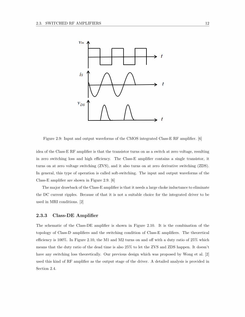
2.3.3 Class-DE Amplifier
The schematic of the Class-DE amplifier is shown in Figure 2.10. It is the combination of the
topology of Class-D amplifiers and the switching condition of Class-E amplifiers. The theoretical
efficiency is 100%. In Figure 2.10, the M1 and M2 turns on and off with a duty ratio of 25% which
means that the duty ratio of the dead time is also 25% to let the ZVS and ZDS happen. It doesn’t
have any switching loss theoretically. Our previous design which was proposed by Wong et al. [2]
used this kind of RF amplifier as the output stage of the driver. A detailed analysis is provided in
Section 2.4.

2.3. SWITCHED RF AMPLIFIERS 13
Figure 2.10: Schematic of the CMOS integrated Class-DE RF amplifier
Figure 2.11: Schematic of the step-up driving circuit

2.3. SWITCHED RF AMPLIFIERS 14
2.3.4 Step-up Driving Circuit
The step-up driving circuit’s schematic is shown in the Figure 2.11. It is derived directly from the
classical step-up DC/DC circuit which is also known as boost-buck converter. The only difference
is the charge storage capacitor is replaced by the parallel capacitor in the equivalent circuit of the
transducer (CP ). The voltage on the transducer terminals depends in the pumping pulse train
switching frequency, duty ratio, inductance L1 and the switch S1, S2 on-resistance [8].
The operating process is: first, both the S1 and S2 turns on to charge up the inductance L1.
Then S2 turns off to let the energy that was stored in the inductor to be transfered to the transducer.
At last, S1 turns off and S3 turns on to discharge the transducer. Because it includes 3 transistors
in the step-up driving circuit, its timing and control circuit can be very complicated and the diode
used in this circuit introduces additional losses [8].
2.3.5 Flyback Topology
The schematic of the flyback topology is shown in Figure 2.12., in this figure, the LP and LS operate
as a transformer, LP connects the supply voltage and switch and LS connects ground and transducer.
By turning switch on and off, that will make the voltage change across the transducer [8].
The major advantage of the flyback topology is that it just needs one transistor to generate the
pulse signal to the transducer [2]. But a major drawback of this topology is that this circuit has a
secondary winding resonance generated by the transducer parasitic capacitance CP , which will cause
long ringing after the switch is open and it needs a transformer which is a magnetic component,
thus it cannot be used in the MRI conditions [8].
2.3.6 Push-pull driving circuit
The push-pull topology is almost the same as the flyback topology, the schematic is shown in Figure
2.13. This topology uses two switches that turn on and off at different times. At start, both switches
are turned off, then the S1 is turned on for the half of the transducer excitation pulse period. After
that it is turned off, but the S2 is turned on [8].
In this topology, the transformer is used to match the impedance of the transducer to maximize
power transfer, but it will occupy a large portion of area and it cannot be used in the MRI conditions,
so this kind of topology will not be applied in our design.

2.3. SWITCHED RF AMPLIFIERS 15
Figure 2.12: Topology of the flyback transducer driver [8]
Figure 2.13: Schematic of the Push-pull driving circuit

2.4. LITERATURE REVIEW 16
2.4 Literature Review
Hall and Cain [9] proposed a Class-D amplifier, whose efficiency is 90% and output power is 20 W,
operating frequency is 1 MHz, for a 512-channel transducer array. Its schematic is shown in Figure
2.14. The two transistors in this schematic form an inverter with the addition of transistor gate
drivers. The duty ratio is decided by the input TTL signal which is a square wave. Tuned filter
inductor L1 and capacitor C1 cancel out the higher harmonics of the square wave. [9]
The advantage of this topology is simplicity and low cost. But there are two resistors (R1 and
R2) in this design, which will occupy a lot of area if we use them in an integrated circuit. Also
the inductor L1 in the filter cannot be used in the MRI conditions. So this kind of topology is not
suitable to our objective.
Figure 2.14: Schematic of the transducer driver which was proposed by Cain and Hall [9].
Tang and Clement [7] discussed the harmonic cancellation technique for a therapeutic ultrasound
transducer in HIFU applications. The schematic of the driver that they used is shown in Figure
2.15. It contains two power converters in cascade and the operating frequency is 1 MHz. [7]
In their work, they point out that driving a piezoelectric ultrasound transducer in HIFU appli-
cations with a signal that contains harmonics will distort the shape of the ultrasound focal zone.
This is because the harmonic in the driving signal will lead the transducer to generate unwanted
sidelobes in the acoustic field. These sidelobes have extra energy and will distort the shape of the
focal zone. So the harmonic cancellation technique was introduced to solve this problem. [7]
The harmonic cancellation technique uses a pre-calculated firing angle of the driving signal which

2.4. LITERATURE REVIEW 17
is a square wave pulse train. As shown in Figure 2.16, the square wave has a firing angle of π/3
which eliminates the third harmonic. This technique does not require an LC filter circuit. [7]
However this design requires two transformers in the circuit which is not suitable for MRI.
Also this harmonic cancellation technique must be very precise. Rise time and fall time must be
minimized, otherwise, the unwanted harmonic will appear at the output of the driver. So this design
is not suitable for our objective. [7]
Figure 2.15: Schematic of the driver that is used by Tang and Clement [7]
Yang and Xu [10] used a Class-D full-bridge amplifier to drive an Audio Beam system. The
schematic of this driver is shown in Figure 2.17. The switching operating frequency is 600 kHz, and
the Audio Beam System can generate a highly concentrated audio signals between 20 kHz to 60 kHz.
There are two resistors R1 and R2 and an operational amplifier in this circuit to cooperate with the
gate driver IC to make an over current protection for the MOSFETs at the output stage. Inductors
L1 and L2 are connected with the transducer to make a reduction of instantaneous current that
flows through the loaded transducer.
Because of the inductors and the resistors in this design, it will occupy a large portion of area
and interfere the operation of MRI, so we cannot employ this design in our project.
D. Zhao et al. [11] proposed a high voltage pulser for ultrasound medical imaging applications.
The schematic of their design is shown in Figure 2.18. This circuit is a Class-D amplifier with a

2.4. LITERATURE REVIEW 18
Figure 2.16: Input waveform of the driver that is used by Tang and Clement [7]
Figure 2.17: Schematic of driver that is proposed by Yang and Xu [10].
2.4. LITERATURE REVIEW 19
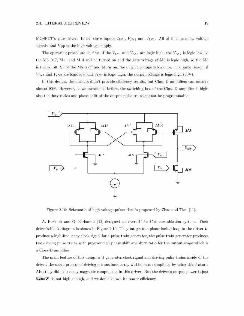
MOSFET’s gate driver. It has three inputs VIN1, VIN2 and VIN3. All of them are low voltage
signals, and Vpp is the high voltage supply.
The operating procedure is: first, if the VIN1 and VIN3 are logic high, the VIN2 is logic low, so
the M6, M7, M11 and M13 will be turned on and the gate voltage of M5 is logic high, so the M5
is turned off. Since the M5 is off and M6 is on, the output voltage is logic low. For same reason, if
VIN1 and VIN3 are logic low and VIN2 is logic high, the output voltage is logic high (30V).
In this design, the authors didn’t provide efficiency results, but Class-D amplifiers can achieve
almost 90%. However, as we mentioned before, the switching loss of the Class-D amplifier is high;
also the duty ratios and phase shift of the output pulse trains cannot be programmable.
Figure 2.18: Schematic of high voltage pulser that is proposed by Zhao and Tian [11].
A. Bozkurk and O. Farhanieh [12] designed a driver IC for Catheter ablation system. Their
driver’s block diagram is shown in Figure 2.19. They integrate a phase locked loop in the driver to
produce a high-frequency clock signal for a pulse train generator, the pulse train generator produces
two driving pulse trains with programmed phase shift and duty ratio for the output stage which is
a Class-D amplifier.
The main feature of this design is it generates clock signal and driving pulse trains inside of the
driver, the setup process of driving a transducer array will be much simplified by using this feature.
Also they didn’t use any magnetic components in this driver. But the driver’s output power is just
530mW, is not high enough, and we don’t known its power efficiency.

2.5. PREVIOUS DESIGN BY OUR GROUP 20
Figure 2.19: Block diagram of A. Bozkurk and O. Farhanieh’s driver IC [12]
K. Moro and J. Okada [13] designed a staircase-wave drive circuit to drive therapeutic array
transducers. Their circuit is shown in Figure 2.20 and the waveforms of the schematic are shown in
Figure 2.21. In the schematic, the VPP1 is higher than VPP2. As shown in the Figure 2.21, the M3 is
turned on first, so the output voltage is equal to VPP2, and then M1 is turned on and off for a while,
it generates a higher voltage pulse which is equal to VPP1. When the M1 is turned off, the output
voltage waveform falls back to VPP2. In this process, a half period of staircase-wave is presented at
the output. If we turned on and off M3 and M4 by the same procedure, a negative staircase-wave
will be presented at the output. By using this stair-wave, the third and fifth harmonics will be
reduced to zero, but the switching loss cannot be eliminated. It also needs a large portion of area
to fit the 4 resistors in this design if we fabricate this circuit in a chip.
2.5 Previous Design by Our Group
Our previous ultrasound transducer driver design was proposed by W. Wong et al. [1,2,5]. A Class-
DE amplifier is driven by two gate drivers (Figure 2.22). This driver is implemented by using AMS
H35B4 CMOS technology.
The operation of the Class-DE amplifier can be divided in 4 intervals. Figure 2.23 shows the
voltage and current waveforms of the whole operation period and Figure 2.20 shows the equivalent
circuits for each interval.
Interval 1
Between ωt0 radians and π. Transistor M1 turns on and M2 turns off. The equivalent circuit is
shown in Figure 2.24(a). The current iM1 slowly increases from 0 until its peak and then decreases
until ωt = π. The drain potential of M2 is at highest potential(Vcc) in this whole interval, so no

2.5. PREVIOUS DESIGN BY OUR GROUP 21
Figure 2.20: Schematic of staircase-wave driver that is proposed by K. Moro and J. Okada. [13]
current flow through the parallel capacitor CP . The current iM1 will be the only current that charges
the series resonance branch [2]. In this interval the output voltage is Vcc.
Interval 2
Between π and π + ωt0. Both transistors M1 and M2 are turned off. The equivalent circuit of this
interval is shown in Figure 2.24(b). There is no current flow through the transistors in this interval.
So the parallel capacitor will provide the current to the series resonance branch, because the Ls
and Cs maintains the continuity of the load current. Because of that, the load current falls down
sinusoidally to 0 at π + ωt0. Since the CP charges the series resonance branch in this interval, the
voltage across the M2 will be decreased slowly , from Vcc until 0 at π + ωt0. The VDS1 will be
decreased to −V cc at this moment.
Interval 3
Between π + ωt0 and 2π. In this interval the M2 is turned on and M1 is turned off. The equivalent
circuit of this interval is shown in Figure 2.24(c). M2 is turned on when the VDS2 is zero, so the
ZVS and ZDS conditions are reached. Because of the M2 being turned on, the VDS1 is maintained
at −Vcc and no current flows through the CP . The series resonance branch will discharge through
M2, its current keeps decreasing until its lowest peak.

2.5. PREVIOUS DESIGN BY OUR GROUP 22
Figure 2.21: Input and output voltage waveforms of the staircase-wave driver [13]

2.5. PREVIOUS DESIGN BY OUR GROUP 23
Figure 2.22: Schematic of driver that is proposed by Wai Wong. [5]
Figure 2.23: Output waveforms of half-bridge Class-DE amplifier [5]

2.5. PREVIOUS DESIGN BY OUR GROUP 24
Figure 2.24: Equivalent circuits of Class-DE amplifier in each interval. [6]

2.5. PREVIOUS DESIGN BY OUR GROUP 25
Interval 4
Between 2π and 2π + ωt0. In this interval both M1 and M2 are turned off. The equivalent circuit
of this interval is shown in Figure 2.24(d). Because of Cs and Ls, the series resonance branch keep
discharging in this interval. Because of M2 being turned off, the load current will flow through CP
to charge it and let the VDS2 increase, at the end of this interval which is at 2π+ωt0, the VDS2 will
reach its highest point that is Vcc. After 2π, its the fifth interval which is same as the first one, the
M1 will be turned on and M2 will be turned off. At the moment that M1 is turned on which is at
ωt = 2π + ωt0 the VDS1 is equal to zero which matches the ZVS and ZDS conditions again.
If we want to drive an ultrasound transducer by using this design, we must decide its operating
frequency (f) and corresponding duty ratio (D) to maximize the power transmission efficiency. The
expression of the output voltage and load current of the Class-DE amplifier in the interval 2 and 4
is [14]:
vOUT = VCC2cos(ωt− φ)− (1 + cosφ)
2(1− cosφ)t ∈ [0 + kπ, t0 + kπ], k = 0, 1, 2 . . . (2.6)
i = Imsin(ωt− φ) (2.7)
where the φ is an angle that relate to the duty ratio D by equation φ = π(1 − 2D), the φ
cannot be zero, because when φ = 0 the duty ratio is 50%, then the Class-DE condition is no longer
exist. Then we can get the fundamental component of VOUT and load current i by using Fourier
analysis [14]:
V1 =4
T
(∫ t0
0
vDS2(t)exp(−jωt)dt+
∫ T/2
t0
VCC2
exp(−jωt)dt
)(2.8)
I1 =2
T
∫ T
0
Imsin(ωt− φ)exp(−jωt)dt (2.9)
The fundamental components of the output voltage VOUT and load current i are shown below
(please note that VCC = 1CP
∫i(t)dt) [14]:
V1 = VCCφcosφ− sinφ− jφsinφ
π(1− cosφ)(2.10)

2.5. PREVIOUS DESIGN BY OUR GROUP 26
I1 = −ωCPVCC(sinφ+ jcosφ)
1− cosφ(2.11)
If we substitute the equation (2.10) and (2.11) to equation Z = V/I, we can get the expression
of the load impedance ZL [5, 14]:
ZL =V1I1
=1− cos(2φ)
2πωCP+ j
2φ− sin(2φ)
2πωCP(2.12)
In Equation 2.12, the real part and imaginary part of ZL are [5]:
RL =1− cos(2φ)
2πωCP(2.13)
XL =2φ− sin(2φ)
2πωCP(2.14)
From Equation (2.1)
ZL = RS + jωLS +1
jωCS(2.15)
So, let the RL = RS , XL = jωLS + 1jωCS
and solve them for frequency [5]:
fr =1− cos(2φ)
4π2CPRS(2.16)
fx =1
2π
√2φ− sin(2φ)
2πCPLS+
1
CSLS(2.17)
where the fr is the frequency that we get from the real part of the impedance and fx is the
frequency that we get from the imaginary part of impedance. Equations (2.16) and (2.17) are
functions of duty ratio D. If we plot these two equations in a duty ratio range [0.1,0.4], we can get
the operation frequency and corresponding duty ratio of the Class-DE amplifier. For instance, in
Figure 2.25 we plot fr and fx for a transducer that has the equivalent circuit values that are shown
in Table 2.1: In this Figure the black line represents the plot of the fr and red line represent the
CP CS LS RS827pF 183pF 139uH 40.25Ω
Table 2.1: Equivalent circuit’s parameters of an ultrasound transducer.
plot of fx. As we can see, there are two intersection points of these two lines in this figure, these are

2.5. PREVIOUS DESIGN BY OUR GROUP 27
Figure 2.25: Variations of fr and fx with duty ratio of an ultrasound transducer
the points that Class-DE mode switching happens(fr = fx). If we substitute equations (2.16) and
(2.17) into fr = fx, we can find the optimum Class-DE switching frequencies and the corresponding
duty ratios for this transducer. The optimum frequencies and corresponding duty ratios are shown
in Table 2.2.
D1 = 0.160 f1 = 1084kHzD2 = 0.348 f2 = 1014kHz
Table 2.2: Optimum Class-DE switching frequencies and duty ratios of the instance transducer.
Because of the series resonance frequency of this transducer being fs = 1/(2π√LsCs) ≈ 1MHz,
the operating frequency must be closest to it. That means we should use the f2 and D2 as the
operating frequency and duty ratio. Also, because the D2 is larger than D1, using D2 and f2 will let
the transistors turned on time is longer than using D1 and f1, which means more output power [5].
The efficiency of the transducer driver designed in [5] is 90% and there is no magnetic components,
such as inductors and transformers, in this circuit, which means that we can use this driver in MRI
conditions. Also the circuitry of this design is very simple, it won’t occupy a large portion of area,
so we can integrate it in a chip. The power will be delivered to the transducer by the driver is over
1 W which means we have achieved our minimum goal [5].

2.5. PREVIOUS DESIGN BY OUR GROUP 28
However, in this design the driving signals, which are pulse trains, of both transistors in the
Class-DE amplifier are not generated by the driver itself. Instead external signals must be provided
to the transducer driver. Because of that, the connection setup of the driver would be very complex
in a large transducer array. If we want to decrease the complexity of the connection setup, we should
internally generate the pulse trains that drive the switches of the Class-DE amplifier. The phase
shift and duty ratios should be digitally programmable through an interface that is common to all
drivers in an array (phase shifts determines when φisgetstarted and duty ratio determines the value
of φ).
Some of transducers do not have Class-DE switching points, which means that they cannot
be driven by Class-DE amplifiers. For instance,a transducer such as the one described in Table
2.3(Tx.3) [15].
CP (pF ) CS(pF ) LS(mH) RS(kΩ)473 15 6.5 1.116
Table 2.3: Equivalent circuit components’ values of Tx.3
If we substitute these values to the equation 2.16 and 2.17 and plot them, we obtain curves of
fr and fx that do not intersect (see Figure 2.26. In this case, if we want to drive this transducer
by using Class-DE amplifiers, either an external matching network is required or the amplifier has
to be driven in sub-optimal conditions near the series resonance frequency of the transducer, since
at the series resonance frequency the transducer can get highest power delivery. Due to the MR
environment concern, we can not use an external matching network in this case, which means driving
it in sub-optimal condition is the only choice. In order to find the best duty ratio in this case, a
duty ratio sweep can be used. Figure 2.27 shows the effect of duty ratio on efficiency,output power
and current peak when the transducer is driven at the series resonance frequency. We can then
use this sweep to use the operating duty cycle that allow for the maximum efficiency despite the
sub-optimum condition.
As we can see in this figure, the transducer Tx.3’s efficiency reaches its maximum when duty
ratio is near 0.25, so we choose 0.25 as the operating duty ratio for driving the transducer Tx.3.
The output waveforms are shown in Figure 2.28. The amplifier is not operating in Class-DE mode
and the output current waveform has high peaks, caused by the MOSFETs turning on when the
voltage across the drain and source is not zero. The average current peak value is 1.06A, the current
peaks width (41.22764µs − 41.19224µs = 0.0354µs) is shown in this Figure. Table 2.4 summarizes
DC supply power, output power and efficiency for transducer Tx.3.

2.5. PREVIOUS DESIGN BY OUR GROUP 29
0.1 0.15 0.2 0.25 0.3 0.35 0.40
1
2
3
4
5
6x 10
5
Duty Ratio
Fre
qu
en
cy(H
z)
fr
fx
Figure 2.26: fr and fx plots of transducer Tx.3
Figure 2.27: Effect of duty ratio on efficiency,output power and current peak with variable dutyratios
DC supply power(mW) Output power (mW) Efficiency(%)524 227 43.3
Table 2.4: DC supply power, output power and efficiency for transducer Tx.3

2.6. SUMMARY 30
Figure 2.28: Output waveforms for transducer Tx.3
2.6 Summary
Overall, the Class-DE amplifier that was used in [5] is more suitable for our objectives than others.
Because of that, the works that are presented in this thesis intend to upgrade that design to include
the phase shift, driving frequency and duty ratios as programmable parameters. Furthermore, we
intend to make the driver capable of delivering more power to the transducer. The comparison of
the reviewed works is shown in Table 2.5.

2.6. SUMMARY 31
Topology or Ref-erence
Waveforms Efficiency Power Comments
Hall and Cain’sdesign [9]
PWM Wave Over 90% 20W Need a LC match-ing network.
Tang andClement’s de-sign [7]
Sinusoidal Wave 90% Unknown Needs a trans-former.
Yang and Xu’s de-sign [10]
PWM Unknown Unknown Needs a inductor
Zhao et al.’s de-sign [11]
Square Wave Unknown Unknown Switching loss ishigh
Moro and Okada’sdesign [13]
Staircase Wave Unknown Unknown Switching loss ishigh and need alarge portion ofarea for the resis-tors
A. Bozkurk andO. Farhanieh’s de-sign [12]
Square Wave Unknown 530mW Output power isnot high enough
W.Wong andC.Christoffersen’sdesign [2, 5]
Class-DE Wave 90% 1W Duty ratios andphase shifts non-programmable
Table 2.5: Comparison of some published works

Chapter 3
Strategy to Drive a Transducer
array in Class-DE Mode
Figure 3.1: Multi-element ultrasound transducer array that was designed by J. L. Kivinen [4]
In last chapter, it was stated that the half-bridge Class-DE amplifier proposed in [5] is suitable
to the objectives, it can deliver enough power and the efficiency is high. If we want to apply this
ultrasound transducer driver in a MRI conditions for HIFU applications, we must use it to drive a
multi-element transducer array which might include over 1000 elements. Since the transducers in

33
Figure 3.2: Half-bridge Class-DE amplifier which was proposed by Wai Wong [1,2, 5]
an array are not exactly equal, the optimum driving parameters will be different for each individual
transducer. However, all these elements will be driven at the same frequency. Therefore, a strategy
must to be developed to drive an ultrasound transducer array with elements which have different
optimum driving frequencies.
In this Chapter, we will use an ultrasound transducer array designed by J. L. Kivinen [4](Figure
3.1) and the half-bridge Class-DE amplifier proposed by Wai Wong [1, 5] (Figure 3.2). To develop
the multi-element transducer array’s driving strategy. Although this transducer array’s elements can
be used in HIFU applications, but it cannot focus the acoustic waves because of their arrangement
pattern. It is however a good model to help us derive an array driving strategy since it has multiple
piezoelectric elements.
The outline of this Chapter is: Section 3.1 introduced a transducer array and derived its equiv-
alent circuit parameters; Section 3.2 introduced two strategies to drive a transducer array; The
Section 3.3 summarizes this Chapter.

3.1. CHARACTERIZATION OF THE TRANSDUCER ARRAY 34
3.1 Characterization of the Transducer Array
We can plot each element’s real part of the impedance and the real part of admittance of Kivinen’s
transducer array by using a vector network analyzer to find the series resonance frequency (fS) and
the parallel resonance frequency (fP ) of each element and their magnitude of impedance (Z|ω=ωS=
R+ jX). The fS , fP and |Z| are shown in Table 3.1.
Based on these parameters we can get all the equivalent circuit value of these six elements by
Element fS(kHz) fP (kHz) R(Ω) X(Ω)
A 997.5 1102.5 38.6 8.04
B 997.0 1100.0 45.32 8.65
C 1000.0 1110.0 42.3 7.78
D 1000.0 1110.0 38.4 9.27
E 1000.0 1110.1 40.8 7.16
F 1000.0 1110.3 38.0 8.82
Table 3.1: fS , fP and |Z| values of each element of Kivinen’s transducer array
using the Equations 2.2 to 2.5, all the parameters of are shown in Table 3.2, the differences among
transducers can be observed in Table 3.1 and 3.2:
Transducers CP (pF ) CS(pF ) LS(uH) RS(Ω)
A 827 183 139 40.25
B 699 152 167.8 45.32
C 669 155 163.04 43.73
D 945 219 115.43 40.64
E 664 154 164.33 42.06
F 922 214 118.31 40.05
Table 3.2: Equivalent circuit parameters of all the six elements of Kivinen’s transducer array

3.2. THE TRANSDUCER ARRAY DRIVING STRATEGIES 35
3.2 The Transducer Array Driving Strategies
We can get the optimum operation frequency and duty cycles (a transducer will reach its maximum
efficiency when it is driven by its optimum frequency and duty ratio) for all elements in the transducer
array using Equations (2.16) and (2.17). They are shown in the Table 3.3. If every element is driven
Transducer Duty Cycle Operation Frequency(kHz)
A D = 0.348 f = 1014
B D = 0.354 f = 1012
C D = 0.361 f = 1014
D D = 0.328 f = 1024
E D = 0.366 f = 1013
F D = 0.334 f = 1022
Table 3.3: Operation frequencies and duty cycles of all elements in the transducer array
by its own optimum frequency and duty cycle separately, the output voltage and load current
waveforms are shown in Figure 3.3. As we can see, all the elements are driven in Class-DE mode,
but there are some small spikes on the output current waveform, because the input pulse trains need
a rise time or fall time to reach their highest value and lowest value to turn on the transistors so that
the transistors cannot be turned on at the exact time that they should be turned on. The efficiency
when all elements are driven by their own optimum frequencies and duty cycles is shown in Table 3.4
In the table, DC supply power is the power that is provided by power supply and output power is
the power that is delivered to the transducer. As we can see in Table 3.4, all the efficiencies are close
to 92% and the output powers are close to 1 W. In practice, however, we must drive all the elements
at the same frequency (the duty cycle can be different for each element). If we drive a transducer
by using a non-optimum frequency, the switching loss of the Class-DE amplifier will be higher. The
output waveforms of element B when it is driven under a non-optimum frequency 1024kHz is shown
in Figure 3.4, the output waveforms show it is not in Class-DE mode (there are some distortions in
the current waveform). So, to eliminate the switching loss and drive all the elements under a same
frequency, we derived the following two strategies.

3.2. THE TRANSDUCER ARRAY DRIVING STRATEGIES 36
Figure 3.3: Output voltage and current waveforms of all the six elements that are driven by Class-DEamplifier

3.2. THE TRANSDUCER ARRAY DRIVING STRATEGIES 37
Transducers DC supply power(mW) Output power (mW) Efficiency(%)
A 1242 1144 92.1
B 1161 1071 92.2
C 1238 1142 92.3
D 1071 984.4 91.9
E 1300 1200 92.3
F 1145 1053 92
Table 3.4: Simulation results of all the elements in the transducer array
Figure 3.4: Output voltage and current waveforms of element B that is driven under 1024kHz whichis a non-optimum frequency for element B
3.2. THE TRANSDUCER ARRAY DRIVING STRATEGIES 38
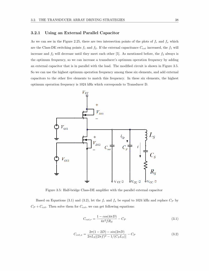
3.2.1 Using an External Parallel Capacitor
As we can see in the Figure 2.25, there are two intersection points of the plots of fr and fx which
are the Class-DE switching points f1 and f2. If the external capacitance Cext increased, the f1 will
increase and f2 will decrease until they meet each other [5]. As mentioned before, the f2 always is
the optimum frequency, so we can increase a transducer’s optimum operation frequency by adding
an external capacitor that is in parallel with the load. The modified circuit is shown in Figure 3.5.
So we can use the highest optimum operation frequency among these six elements, and add external
capacitors to the other five elements to match this frequency. In these six elements, the highest
optimum operation frequency is 1024 kHz which corresponds to Transducer D.
Figure 3.5: Half-bridge Class-DE amplifier with the parallel external capacitor
Based on Equations (3.1) and (3.2), let the fr and fx be equal to 1024 kHz and replace CP by
CP + Cext. Then solve them for Cext, we can get following equations:
Cext,r =1− cos(4πD)
4π2fRS− CP (3.1)
Cext,x =2π(1− 2D)− sin(2πD)
2πLS [(2πf)2 − 1/(CSLS)]− CP (3.2)

3.2. THE TRANSDUCER ARRAY DRIVING STRATEGIES 39
Figure 3.6: Cext,r and Cext,x’s plots of element E in Kivinen’s transducer array
Where Cext,r is the external parallel capacitance which is obtained from solving the equation for
the real part of the transducer’s impedance and Cext,x is the external parallel capacitance that is
obtained from solving the equation for the imaginary part of transducer’s impedance. Then if we let
the Cext,r = Cext,x and solve this equation, we can get the value of this external parallel capacitance
with its corresponding duty ratio.
Let’s use element E as an instance. In Equations (3.1) and (3.2), set f = 1024kHz and plot
Cext,r and Cext,x versus the duty ratio D respectively. We obtain Figure 3.6 where the black line
is the plot of the Cext,r and the red line is the plot of the Cext,x. There is an intersection of these
two plots, the intersection point is the value of the external capacitance with its corresponding duty
ratio. In this instance, the element E’s external capacitance and its corresponding duty ratio is
449pF and 0.287.
Based on above method, we can get all the external capacitance values of these six elements
and their corresponding duty ratios. These values are shown in Table 3.5. The output voltage and
current waveforms of all the 6 elements are shown in Figure 3.7. In this Figure, the periods of all
the transducer elements are same, but their duty ratios are different. Their efficiency results are
shown in Table 3.6. If we compare the efficiency results from Table 3.6 to the efficiency results of
all the elements are driven under same frequency without the Cext, which are shown in Table 3.7,
the efficiencies have been increased.
However, the output power of this method is in some cases much lower than 1 W. Because the
duty ratios are smaller than the optimum duty ratios, the turn on time of each transistor is shorter
and less power is transferred to the load.

3.2. THE TRANSDUCER ARRAY DRIVING STRATEGIES 40
Element D Cext
A 0.291 323pF
B 0.279 356pF
C 0.293 380pF
D 0.328 0
E 0.287 449pF
F 0.323 69pF
Table 3.5: External capacitance values of all the elements in Kivinen’s transducer array
Transducers DC supply power(mW) Output power (mW) Efficiency(%)
A 797 726.8 91.1
B 641.8 579.5 90.3
C 754.7 686.8 91
D 1071 984.4 91.9
E 736.8 669.4 90.9
F 1047 961.1 91.8
Table 3.6: Efficiencies of all the elements that are driven at 1.0242MHz with Cext
Transducers DC supply power(mW) Output power (mW) Efficiency(%)
A 855.5 778.9 91
B 692.9 622.6 89.9
C 817.5 741.2 90.7
D 1071 984.4 91.9
E 816.1 736 90.2
F 1065 977.7 91.8
Table 3.7: Efficiencies of all the six elements that are driven at 1.0242MHz without Cext

3.2. THE TRANSDUCER ARRAY DRIVING STRATEGIES 41
Figure 3.7: Output waveforms of all the elements that are driven by the using the external capacitormethod

3.3. SUMMARY 42
3.2.2 Using the Average frequency
We can obtain more output power with acceptable efficiency by using the average frequency and
optimum duty ratios of each element.
The average of all the optimum operating frequencies of all the six elements is 1017 kHz. Under
this operating frequency, all the elements should have some distortions on their output Voltage and
current waveforms. This will cause more switching loss during the Class-DE switching. However,
if the switching loss is not very high, it should be acceptable. The output voltage and currents of
all the six elements are shown in Figure 3.8. As we can see, there are some distortions on all the
output current waveforms except D compared with the Figure 3.3. Table 3.8 shows the efficiency
results of all the six elements that are driven at the average frequency, all the output power are
higher than the external capacitor method and the efficiency is almost the same. Comparing the
results of average frequency driving to the optimum frequency driving which is shown in Table 3.4,
the total delivered power is the same and the efficiencies are only slightly lower.
Transducers DC supply power(mW) Output power (mW) Efficiency(%)
A 1151 1059 92
B 972.3 891.1 91.7
C 1125 1037 92.1
D 1340 1229 91.8
E 1137 1046 92
F 1345 1236 91.9
Table 3.8: Efficiencies of all elements which are driven by average frequency
3.3 Summary
In this section we introduced two strategies to drive a transducer array under the same frequency,
one uses an external capacitor to make all the elements operate at a higher frequency and the other
drives the elements by using the average of the optimum operating frequencies of all elements. The
external capacitor strategy can remove all the distortions of all the output waveforms and keep
elements operating in high efficiencies. But the major drawback of this strategy is that the output
power is reduced. The average driving strategy cannot remove all the distortions on the output

3.3. SUMMARY 43
Figure 3.8: Output waveforms of all the elements that are driven by the average of their optimumfrequencies

3.3. SUMMARY 44
waveforms, but it still can let the elements operate at high efficiencies while keeping the output
power at a higher level.

Chapter 4
Ultrasonic Transducer Driver
Design
4.1 Introduction
Figure 4.1: Block diagram of the proposed integrated transducer driver [5]
As previously discussed, the final design is a full-bridge Class-DE amplifier with integrated logic
and gate drivers. The block diagram of the final design is shown in Figure 4.1. In this design,

4.2. FULL-BRIDGE CLASS-DE AMPLIFIER 46
we integrated the output stage, gate drivers and digital logic control part in the same chip. The
output stage is a full-bridge Class-DE amplifier which is composed of 4 transistors. The gate driver
is composed by a level shifter and a output stage to amplify the 5 V pulse trains to 20 V pulse trains.
The digital logic control unit is composed by a counter, 3 comparators , a register and a pulse trains
generator. The driver was implemented with Austria Microsystems’ AMS AG H35 CMOS process
using the Cadence R© suite of design tools.
4.2 Full-bridge Class-DE Amplifier
In our proposed design, we chose a full-bridge Class-DE amplifier as the output stage. Its efficiency
is just slightly lower than the half-bridge Class-DE amplifier, because of the full-bridge Class-DE
amplifier’s switch resistance being 2 times of the half-bridge one. On the other hand the output
power can be nearly 4 times higher than the one obtained with the half-bridge. So by using the
full-bridge one we can achieve one of our objectives to deliver more power to the load and keep the
high efficiency at same time.
The high voltage MOSFETs’ symbol is shown in Figure 4.2 (a) and (b), the low voltage MOS-
FETs’ symbol is shown in Figure 4.2 (c) and (d).
Figure 4.2: Symbols of the MOSFETs (a) HV PMOS; (b) HV NMOS; (c) LV PMOS; (d) LV NMOS
The topology of the full-bridge Class-DE amplifier is shown in Figure 4.3. In this figure, the load
transducer has been replaced by its equivalent BVD circuit. The input and output waveforms of the
full-bridge Class-DE amplifier are shown in Figure 4.4.
The full-bridge Class-DE amplifier also has 4 intervals in its operation. These 4 intervals’ princi-
ples are similar to the half-bridge Class-DE amplifier’s which was described in section 2.5, so the ZVS
and ZDS conditions are also satisfied. During interval 1, M1 and M3 are turned on, VOUT = VCC ;
In interval 2, all transistors are turned off, CP is charging the series resonance branch during this
interval, so VOUT decreases to −VCC ; During interval 3, M2 and M4 are turned on, VOUT stay at
−VCC ; During interval 4, all transistors are turned off again, VOUT increases to VCC . compare to
the half-bridge Class-DE amplifier, the output voltage of full-bridge amplifier is doubled and output

4.2. FULL-BRIDGE CLASS-DE AMPLIFIER 47
power is increased 4 times.
Figure 4.3: Topology of the full-bridge Class-DE amplifier
In practice, the channel resistance will produce switching loss in the transistors, and the actual
efficiency of the Class-DE amplifier is not the ideal 100%. From [2] the maximum efficiency of the
half-bridge Class-DE amplifier is nearly 80% and in the [5] the maximum efficiency is over 90%.
The full-bridge Class-DE amplifier is actually a combination of two half-bridge Class-DE ampli-
fier, so we can use the same WL value of half-bridge Class-DE amplifier for the full-bridge one. In [5],
we have the half-bridge Class-DE amplifier’s width and length parameters which are listed in Table
4.1:
PMOS NMOSTransistor finger W/L(µm/µm) 50/1.4 50/1
Number of parallel fingers 360 140
On-resistance 4.17Ω 4.07Ω
Table 4.1: Half-bridge Class-DE amplifier’s width and length parameters [5]
Please note that (W/L) = (W/L)finger ×Nfinger × 2, where (W/L) is the total aspect ratio of
a transistor, (W/L)finger is the finger width and Nfinger is the finger number of the transistor. So
in the full-bridge Class-DE amplifier we can set(WL
)M1,M4
= 36000/1.4 and(WL
)M2,M3
= 14000/1.
The parasitic capacitance of the switches is approximately 70 pF, so we should also consider the
effect of this parasitic capacitance while determining operating frequencies and duty ratios.

4.2. FULL-BRIDGE CLASS-DE AMPLIFIER 48
Figure 4.4: Inputs and output waveforms of the full-bridge Class-DE amplifier, (a), (b), (c) and (d)The switch-on diagram of transistors M1, M2, M3 and M4. (e) The voltage waveform across theload

4.3. THE GATE DRIVER 49
4.3 The Gate driver
The switch MOSFETs operate at a different voltage level than the logic control. Also the gate
capacitance of the switch MOSFETs is very large. For these reasons we need a dedicated gate driver
to drive these MOSFETs in Class-DE operations. The gate driver determines the rise time and fall
time of the gate voltage to let the MOSFETs to be turned on and off on time.
The schematic of the gate driver is shown in Figure 4.5 [16]. This gate driver consists a level
shifter and an output stage. The output stage is composed by a HV NMOS (M4) and a HV PMOS
(M3). The major advantage of the level shifter is that it offers high speed switching without the
need for multiple driving signals and the major drawback is that its power consumption is nearly
2% of maximum output power [2]. The output VOUT is connected to the gate terminal of a switch
MOSFET. So in this design we need four gate drivers.
In gate driver’s schematic, the LV PMOSs M11, M12, M13 and M14 consist of two voltage
mirrors, along with two HV NMOS M7 and M8.These transistors form a level shifter. The level
shifter can raise a reference 0V to 5V signal to a 0V to VCC signal. The working process of this gate
driver is explained below.
When the input signal VIN (the 0V to Vdd low voltage signal) is logic high, M6 and M7 conduct
and M8 is turned off and then M11 and M13 conduct and M12 and M14 are turned off, so the drain
potential of M7 VC is logic low and drain potential of M8 VA = VCC . Therefore M5 is turned off
and M6 conducts, the output voltage VOUT = 0V . If the VIN is logic low, M8 conducts and M7
is turned off, so M12 and M14 are turned on, M11 and M13 turned off. So VA is logic low and
VC = VCC . Then M5 is turned on and M6 is turned off, the output voltage is VOUT = VCC . By
using this method, the gate driver converts the low voltage signal to high voltage signal.
The aspect ratios of all the transistors in this gate driver is listed below [2]:
(WL
)11
=(WL
)12
=(WL
)13
=(WL
)14
=10um
4um(4.1)
(WL
)7
=(WL
)8
=10um
0.5um(4.2)
The output of this gate driver is the inverse signal of the input signal, which means when the
input is logic high, the output is logic low; when the input is logic low and the output is logic high.
As shown in Figure 4.6. The gate driver’s parameters are taken from Wai’s previous design [2].When
the input is logic low, the M8 and M14 are turned on and VA is up to 18.45V which is just 1.55 V
lower than VCC , that means the M5 is in active region, but the gate driver still keeps working. The
reason is that the load is a MOSFET’s gate whose impedance can be assume to be infinity, so we

4.4. DIGITAL LOGIC UNIT 50
Figure 4.5: Schematic of MOSFETs’ gate driver [2, 16].
just need to make the M5 conduct, no matter it is in triode region or active region.
A disadvantage of this design is that the full VCC supply voltage is applied to the switch gates
(VOUT ). This limits the high voltage that can be applied to the chip to 20V (maximum HV gate
voltage) instead of the maximum drain voltage supported by the technology (50V).
4.4 Digital Logic Unit
The function of the digital logic unit is to generate pulse trains to the 4 MOSFETs in the a full-
bridge Class-DE amplifier and make sure the phase shift and duty ratios of the pulse trains can
be programmable. The structure of this digital logic unit is shown in Figure 4.7. It consists a
10-bit-counter, a 30-bit-register, 3 10-bit-comparators and a pulse train generator. The Digital logic
unit has 7 logic input pins. Among these, CLK, EN, reg CLK, reg data and reset are common to
all drivers in an array. Pin A and B are used to address individual drivers in the array. The power
supply pins are also common to all drivers. A digital logic unit can generate 4 pulse trains for each
MOSFET in a full-bridge Class-DE amplifier.
4.4.1 The Structure of Each Block
A. 10-bit-counter
The 10-bit-counter’s function is to divide CLK signal’s frequency by its modulus. The structure of

4.4. DIGITAL LOGIC UNIT 51
Figure 4.6: Input signal and output signal of the gate driver.
Figure 4.7: Structure of the digital logic unit.

4.4. DIGITAL LOGIC UNIT 52
10-bit-counter is shown in Figure 4.8. It consists 10 positive-edge triggered T flip-flops and some
AND gates. This is an synchronous counter which has better performance in the high frequency
range than the asynchronous counter [17], but it occupies more area in the chip. In this schematic,
the external clock signal will be sent to the CLK pin, the counter will count every positive edge of
the pulses. The Reset pin’s function is to reset the counter by logic low, it connects the output of
the comparator A and an input pin of the pulse trains generator. EN pin is the enable signal of the
counter, it also connects the EN pin of the pulse trains generator. Q0 to Q9 is the output of this
counter, they connect to the input pins in comparator A, B and C.
B. 30-bit-register
The schematic of the 30-bit-register is shown in Figure 4.9. This 30-bit-register consists of 30
positive-edge triggered D flip-flops and an AND gate. This register has 5 input pins which are A, B,
reg data, Reset and reg CLK and 30 output pins which are Q0 to Q29. Pin A and B are the selection
pins of the register, set both A and B to logic high will select a certain driver. In a transducer array,
we can arrange the drivers as a matrix which shown as Figure 4.10. In this figure, each green square
represents a driver. After set one driver’s both pin A and B to logic high, we can send the data to
its 30-bit-register. The data at the pin reg data can be sent to the register when the pin reg CLK
meets a positive edge, so this register is a shift register.
The 30-bit-register has been divided into 3 parts, each part has 10 bits. The first 10 bits is
the CLK pulses to be counted for half period (the reason will be mentioned later) of the output
waveforms of the digital logic unit. The second and third parts are counts for turning one MOSFET
on and off, respectively, in each semi-period. These values define the period, phase shift and duty
ratio of the driver.
C. 10-bit-comparator
The schematic of the 10-bit-comparator is shown in Figure 4.11. It consists of 10 XOR gates, 5
two-input OR gates and a 5-input OR gate. It has 20 input pins which are Q0 to Q9 and R0 to
R9. The Q0 to Q9 is connected with the 10 output pins of the 10-bit-counter and R0 to R9 is
connected to the First, second or third 10 output pins in the 30-bit-register. The OUTPUT pin of
this comparator is connected to the pulse trains generator. When the data at Q0 to Q9 is equal
to the data at R0 to R9, the output of the 10-bit-comparator will generate a negative pulse (its
pulse width is same as a CLK signal’s pulse width), otherwise the OUTPUT pin remains logic high.
By this method, the comparator A can send reset signal to control the 10-bit-counter’s modulus,
comparators B and C can generate start and stop signals of duty cycles and send them to pulse train

4.4. DIGITAL LOGIC UNIT 53
Figure 4.8: Structure of 10-bit-counter.

4.4. DIGITAL LOGIC UNIT 54
Figure 4.9: Schematic of 30-bit-register.
Figure 4.10: Transducer array driving method.

4.4. DIGITAL LOGIC UNIT 55
Figure 4.11: Schematic of the 10-bit-comparator.
generator.
D. Pulse Train Generator
The pulse train generator consists of two positive edge triggered T flip-flops, an inverter, a NAND
gate, 2 OR gates and 2 AND gates. Its schematic is shown in Figure 4.12. It has 5 input pins which
are RN, EN, VDD, START and STOP, 4 output pins which are Pulse P1, Pulse N1, Pulse P2 and
Pulse N2. The EN is the enable pin, it is connected to the EN pin of the counter; RN pin is connected
to the OUTPUT pin of the comparator A which is the reset signal of the 10-bit-counter, represents
the period; START and STOP pins are connected to the OUTPUT pins of the comparator B and
C which are the signal of the start and stop time of the pulse; the output pins Pulse P1, Pulse N1,
Pulse P2 and Pulse N2 are the driving signal of the gate drivers of the M1, M2, M3 and M4 in the
full-bridge Class-DE amplifier respectively.
When EN is set to logic high, the pulse train generator can work normally; if it is set to logic low,
the output of the two T flip-flops will be set to zero, then the Pulse P1 is set to high, Pulse N1 is set
to low, Pulse P2 is set to logic high and Pulse N2 is set to logic low, which means all the MOSFETs
in the full-bridge Class-DE amplifier have been turned off. If the EN goes high, this pulse train
generator can generate the objective pulse trains for the four MOSFETs in the Class-DE amplifier.

4.4. DIGITAL LOGIC UNIT 56
Figure 4.12: Schematic of the pulse-trains-generator.
The working procedure of the whole digital logic unit will be described in the next Sub-section.
4.4.2 Operating procedure of the digital logic unit
The digital logic unit can be divided to 3 parts, the first one is a frequency divider, the second one
is a phase shift and duty ratio controller and the third one is the pulse trains generator. The block
diagram of the relationship of these three parts are shown in Figure 4.13. The operating procedure
is shown below:
A. Frequency Divider
The block diagram of the frequency divider is shown in Figure 4.14. First, when the EN input
goes high, the 10-bit-counter counts the number of the external clock signal’s pulse (CLK). The
external CLK is normally set to a multiple of the transducer operating frequency. The counter’s
modulus controls the resolution of the duty ratio and phase shift. The output of the counter will
be compared with the first 10 bits of the 10-bit-register in comparator A, if they match each other
the comparator A will outputs a negative pulse to the pulse train generator and reset the counter,
otherwise its OUTPUT pin will stay on logic high. The output diagrams are shown in Figure 4.15.
B. Phase Shift and Duty Ratio Controller
The block diagram of the phase shift and duty ratio controller is shown in Figure 4.16. It consists
of two comparators. In the operation of the digital logic unit, the comparator B and C compare the
output of the 10-bit-counter to the second and third 10 bits of the register, if the counter’s output

4.4. DIGITAL LOGIC UNIT 57
Figure 4.13: Block diagrams of the relationship of the frequency divider, phase shift and duty ratiocontroller and pulse train generator.
Figure 4.14: Block diagram of the frequency divider.

4.4. DIGITAL LOGIC UNIT 58
Figure 4.15: Output diagrams of the frequency divider.
matches the data stored in the second and third 10 bits of the register, these two comparators will
generate negative pulses which are the start and stop signal of a duty cycle (START and STOP) ,
otherwise their outputs will remain on logic high. Because of that, the data stored in the third 10
bits of the register must greater than the data stored in the second 10 bits and both of them must
be smaller than the data stored in first 10 bits. The output diagrams are shown in Figure 4.17.
C. Pulse Train Generator
In this part the only component is the pulse trains generator itself. The initial state of both the two
T flip-flops are zero. The input and output diagrams are shown in Figure 4.18.
As shown in the Figure 4.18, when the 10-bit-counter finished the first counting round, com-
parator A will generate a negative pulse to the RN pin of the pulse train generator. Because we
have already set the T pins of both T flip-flop to logic high (as shown in Figure 4.12), the Q1 will
be logic high and QN1 will be logic low, but the Q2 still is logic low and QN2 is still logic high,
so the Pulse P1 and Pulse P2 are logic high, Pulse N1 and Pulse N2 are logic low, which means
all the MOSFETs are still turned off. When the START signal become logic low and STOP signal
remains in logic high, which means the counter’s output matches the second 10 bits of the register
but still doesn’t match the third 10 bits, the Q2 will be logic high and QN2 will be logic low. So the

4.4. DIGITAL LOGIC UNIT 59
Figure 4.16: Block diagram of the phase shift and duty ratios controller.
Figure 4.17: Output diagrams of the phase shift and duty ratios controller.

4.4. DIGITAL LOGIC UNIT 60
Pulse P1 is logic high, Pulse N1 is logic high, Pulse P2 is logic low and Pulse N2 is logic low, that
means the M1 and M3 are turned off, M2 and M4 are turned on. When the output of the counter
matches the data of the third 10 bits of the register, Q2 is set to logic logic low and QN2 is set to
logic high, then Pulse P1 and Pulse P2 are set to logic high, Pulse N1 and Pulse N2 are set to logic
low. Because of that all the MOSFETs are turned off.
When the 10-bit-counter finished the second round of counting , the pulse trains generator’s pin
RN will receive another negative pulse from the comparator A, so Q1 will be logic low and QN1 will
be logic high, but the Q2 is still stays on logic low and QN2 is still stays on logic high, which means
all the MOSFETs are still turned off. When the output of the counter meets the data that is stored
in the second 10 bits of the register, the Q2 will be logic high and QN2 will be logic low again, so
in this time the Pulse P1 and Pulse N1 will be logic low, Pulse P2 and Pulse N2 will be logic high,
which means that the M1 and M3 are turned on, M2 and M4 are turned off. When the output of
the counter matches the third 10 bits of the register, the Q2 is set to logic low and QN2 are logic
high again, then the Pulse P1 and Pulse P2 go logic high, Pulse N1 and Pulse N2 go logic low, all
the MOSFETs in the full-bridge Class-DE amplifier are turned off.
By repeating the procedure described above the M1 and M3, M2 and M4 will be turned on and
off alternatively , to make the full-bridge Class-DE switching occurs.
4.4.3 Additional Safety Logic Block
Two additional safety logic block have been implemented with the digital logic unit to provide the
functions of power stage enabling, output stage buffering and the faulty signal filtering, to make sure
that the NMOS and PMOS in a same branch of the full-bridge Class-DE amplifier won’t be turned
on at same time [2]. They are located prior to the MOSFETs’ gate drivers. The PMOS and NMOS
in same branch share a same additional safety logic block. The schematic of the additional safety
logic block is shown in Figure 4.19. This additional safety logic block’s power supply is standard 5V,
it has 3 input pins and 4 output pins. The input pins are EN which is connected to the EN signal
of the pulse trains generator and 10-bit-counter, P which is connected to the Pulse P1 or Pulse P2
on the pulse train generator, N which is connected to the Pulse N1 or Pulse N2 on the pulse trains
generator. The two outputs are Pout and Nout, the Nout is connected to the one of the gate driver’s
input of the NMOSs in Class-DE amplifier and Pout is connected to the one of the gate driver’s
input of the PMOSs in Class-DE amplifier. The P comp and N comp are the complimentary signals
of the Pout and Nout. Because of the gate drivers’ output signals are the inverse of their input
signals, as we mentioned in Section 4.4, the Pout and Nout must to be the inverse signal of the input
P and N; and also all the four output pins must can handle the large capacitor loads from the gate

4.4. DIGITAL LOGIC UNIT 61
Figure 4.18: Input and output diagrams of the pulse trains generator.

4.4. DIGITAL LOGIC UNIT 62
Figure 4.19: Schematic of the additional safety logic block [2].
driver.
The Yp and Yn are the output signals before inverted. If we ignore the delay, they have same
phase shifts with the input signals of the PMOSs and NMOSs in the Class-DE amplifier (the input
signals of the PMOSs and NMOSs are the output signals of the gate drivers). When the EN input
goes low the Yp is logic high and Yn is logic low, which means the PMOSs and NMOSs are biased
in cut-off mode; when the EN goes logic high, the additional safety logic block is enabled and Yn
and Yp will follow the respective inputs unless the faulty inputs occurs (when P is logic low and N
is logic high, which means the PMOS and NMOS in same branch are turned on at same time).When
the P is logic low and N is logic high, the Yn is set to be logic low and Yp is set to be logic high,
so the NMOS and PMOS in the same branch are in cut-off mode. This process will avoid the faulty
state. The truth table of this additional safety logic block is shown in Table 4.2.
4.4.4 Simulation Results of Digital Logic Unit
In the simulation of the digital logic unit, we want to check not also its functionality, but also its
high frequency performance. In order to make the result clear and easy to check, we used a 200
MHz external clock signal to generate 20 MHz, 36 phase shift and 72 duty ratio pulse trains for
the NMOSs and PMOSs in the Class-DE amplifier.
Based on the setup strategy we mentioned before, we first set pin A and pin B to logic high
and send the data that represent the frequency, start and stop time of the duty cycle to the 30-bit-
register. The intended data is 3, 1 and 5 for each 10 bits of register. We put the data of stop time
of the duty cycle first and the second 10 bits is the start time of the duty cycle, the third 10 bits is
the parameter of the frequency. After that, set the EN pin to logic high, we can get the objective
pulse trains from the output pins.

4.4. DIGITAL LOGIC UNIT 63
EN P N Yp Yn PMOS NMOS0 0 0 1 0 off off
0 0 1 1 0 off off
0 1 0 1 0 off off
0 1 1 1 0 off off
1 0 0 0 0 on off
1 0 1 1 0 off off
1 1 0 1 0 off off
1 1 1 1 1 off on
Table 4.2: Truth table of the additional safety logic block [2]
The simulation results are shown in Figure 4.20. In this figure, the first signal is the external
CLK signal that is sent to the counter, then the comparator A, B and C generates the second and
third signals which are the negative pulses of the period, start time and the stop time of the driver’s
output. The last four signals are the driving signals of M1, M3, M2 and M4 respectively. As we
can see, the M1 and M3 are turned on at same time, M2 and M4 are turned on at same time. The
four driving signals have a little bit delay, but all the signals are passed through the same number
of stages, so the delay time is almost equal for all of them.

4.4. DIGITAL LOGIC UNIT 64
Figure 4.20: Outputs waveforms of the digital logic unit, its input clock signal’s frequency is 200MHz,phase shift is 10%, duty ratio is 20% .

4.5. THE LAYOUT DESIGN 65
4.5 The Layout Design
We used a 2mm × 1.5mm die area to fabricate the chip. We used a Kyocera’s JLCC-28 package
which can accommodate just one die because of the available pin number concern. The layout view
is shown in Figure 4.21. The red blocks which have black comments are the cells described in this
chapter. M1, M2, M3 and M4 are the MOSFETs that form the full-bridge Class-DE amplifier.
They are sized to provide same on-resistance, so the PMOSs is much wider than the NMOSs [5].
Gate drivers are located near each MOSFET. The gate drivers that are in a same branch share a
common current source. The digital logic unit consists of a 10-bit-counter, a 30-bit-register, a pulse
train generator and 3 10-bit-comparators and is located near the second branch of the full-bridge
Class-DE amplifier.
The blue blocks are the pins of this driver, VDD20V and GND20V are the pins of the 20V power
supply of the Class-DE amplifier and gate drivers, VDD5V and GND5V are the 5V supply of the
logic unit and gate drivers, Reg D and Reg C are the reg data and reg CLK of the register as we
mentioned before. Psub is the connection of the substrate (ground), Vm o and Vm in is the output
and input of the current mirror that is shared by the gate drivers. The En, CLK, A, B and Reset
we have mentioned in section 4.4.

4.5. THE LAYOUT DESIGN 66
Figure 4.21: Layout view of the driver

Chapter 5
Simulation and Experimental
Results
All simulations presented in this chapter were generated using the Spectre R© simulator using the
schematic view.
5.1 Simulation Results with Optimum Parameters
The full-bridge Class-DE driver’s simulation results are shown in Figure 5.1. The load is the trans-
ducer from [5]. Equivalent circuit parameters are listed in Table 5.1 and optimum driving parameters
are f = 1010 kHz and D = 29.5%. The output voltage range is from -20V to 20V. Figure 5.2 shows
simulation results of the half-bridge Class-DE driver for the same transducer. Its output voltage
range is from 0V to 20V. Since the full-bridge Class-DE driver has 2 outputs (Output1 and Out-
put2), there are two extra voltage waveforms which are taken from these two outputs. DC supply
power, output power and efficiencies of these two drivers are shown in Table 5.2. As we can see,
the efficiencies of these two drivers are close to each other, but the output power of the full-bridge
driver is nearly 4 times of the half-bridge one’s.
CP (nF ) CS(pF ) LS(uH) RS(Ω)
1.39 340 78.6 31.9
Table 5.1: Equivalent circuit parameters of the transducer [5]

5.1. SIMULATION RESULTS WITH OPTIMUM PARAMETERS 68
Figure 5.1: Simulation results of the full-bridge Class-DE driver that is proposed in this thesis.Brown: output voltage (Output1-Output2); Red: potential of Output1; Pink: potential of Output2;Orange: load current

5.1. SIMULATION RESULTS WITH OPTIMUM PARAMETERS 69
Figure 5.2: Simulation results of the half-bridge Class-DE driver that was designed by our group [5].Brown: output voltage ; Red: load current

5.2. EXPERIMENTAL SETUP 70
Driver DC Supply Power(W) Output Power(W) Efficiency(%)
Full-bridge Class-DE driver 4.02 3.59 89.4Half-bridge Class-DE driver 1.04 0.95 91.5
Table 5.2: DC supply power, output power and efficiencies of driving the transducer by full-bridgeand half-bridge Class-DE drivers
Figure 5.3: Fabricated driver in a testing circuit.
5.2 Experimental Setup
The driver has been fabricated. Initially Kyocera’s LCC 02046 package was going to be used. This
package should be MRI compatible because it has a gold plating instead of nickel plating. For
lowering packaging cost the five packaged samples use a different package: Kyocera’s JLCC-28.
Unfortunately this package is not compatible with MRI imaging because it has a nickel plating
under the gold plating. For this reason it may not be possible to test these packaged samples in the
MRI environment. However, we still can make some tests. Figure 5.3 is the driver which is tested
by using a bread board. We used a function generator (its maximum signal frequency is 15 MHz) to
generate the external CLK signal and an Arduino Uno to program the duty ratios and phase shifts
of the output pulse trains.
First, we tested the logic function of the driver. For example, if we want a load frequency of 187.5
kHz, 45 phase shift and 12.5% duty ratio pulse train, we should send 40, 10 and 20 to the 30-bit
register when the CLK signal is 15MHz. The load is a 10kΩ (9.884kΩ) resistor and the DC supply
is 10V (we used a 10 V DC supply instead of 20V to reduce overheating risk). The output waveform

5.2. EXPERIMENTAL SETUP 71
Figure 5.4: Logic test result of the driver.
is shown in Figure 5.4. As we can see, the output pulse trains swing is from -10V to 10V, the duty
ratio is approximately 12.5% , the distortions on the ends of pulses are caused by the total parasitic
capacitance (caused by the bread board, the probe and load etc.) and switch capacitance. The
combination of total parasitic capacitance and switch capacitance can be expressed as an external
capacitance Cext (Figure 3.5). The Cext can be extracted from Figure 5.4, the 90% and 10% rise
time (t90% and t10%, respectively) of the output voltage’s negative half cycle are approximately 4.98
µs and 2.20us, respectively. These times satisfy the following equations:
90%VCC = VCC(1− exp(− t90%RloadCext
)) (5.1)
10%VCC = VCC(1− exp(− t10%RloadCext
)) (5.2)
If we substitute t90% = 4.98µs and t10% = 2.20µs into these equations, we can get the Cext ≈ 128
pF. Because of the switch capacitance is 70 pF (section 4.2), the total parasitic capacitance is
approximately 58pF.
We tested this driver by letting it drive the transducer simulated in Section 5.1. The block
diagram of the testing setup is shown in Figure 5.5. The driver drives a transducer connected using
a 20 cm long coaxial cable. The optimum frequency and duty ratio of the transducer are modified

5.3. EXPERIMENTAL RESULTS 72
Figure 5.5: Block diagram of the testing setup of the driver
to 1028 kHz and 25.2% by Cext.
We was intended to use a 102.8 MHz (which is 100 times of the transducer’s optimum frequency)
CLK signal, and send 50, 0 and 25 to each 10 bits of the 30-bit-register. But the maximum output
frequency of the function generator is 15 MHz and also the driver is mounted on a bread board, the
CLK signal’s frequency cannot be too high. So we used a 8224 kHz CLK signal and sent 4, 0 and 2
to the driver’s register for a 1028 kHz, 0 phase shift and 25% duty ratio (the closest condition we
can get) pulse train.
5.3 Experimental Results
Figure 5.6 shows simulation results of driving the transducer simulated in Section 5.1 by using a 1028
kHz, 0 phase shift and 25% duty ratio pulse train (the parameters that were mentioned in Section
5.2). During the experimental test, we manually adjusted the frequency to obtain the best output
waveforms at f = 1036 kHz. Experimental results are shown in Figure 5.7, the bottom waveform
is taken from the pin Output2 and the middle one is taken from the pin Output1, the uppermost
waveform is the Class-DE wave which drives transducer (Output1-Output2). A simulation with
f = 1036 kHz is shown in Figure 5.8. Comparing to the simulation waveforms, the uppermost
waveform is nearly a Class-DE waveform and matches the simulation result, but the waveforms of
Output1 and Output2 are much worse, they have many distortions. These distortions may be caused
by following two reasons:

5.3. EXPERIMENTAL RESULTS 73
1. The bread board’s parasitic capacitance at the Output1 and Output2 are asymmetric.
2. The loads of the coaxial cable’s two nodes that connect the driver and transducer are asym-
metric

5.3. EXPERIMENTAL RESULTS 74
Figure 5.6: Simulation results of driving the transducer with Cext = 128 pF by 1028 kHz, 0 phaseshift and 25% duty ratio pulse trains. Brown: output voltage (Output1-Output2); Red: potentialof Output1; Pink: potential of Output2; Orange: load current

5.3. EXPERIMENTAL RESULTS 75
Figure 5.7: Experimental result of driving the transducer by 1036 kHz and 25% duty ratio pulsetrains.

5.3. EXPERIMENTAL RESULTS 76
Figure 5.8: Simulation results of driving the transducer with Cext = 128 pF by 1036 kHz, 0 phaseshift and 25% duty ratio pulse trains. Brown: output voltage (Output1-Output2); Red: potentialof Output1; Pink: potential of Output2; Orange: load current
Chapter 6
Conclusions and Future Work
6.1 Conclusions
The objective of this thesis was to design a CMOS driver for an ultrasound transducer array to be
installed within the MRI environment. Some design challenges have been met. The driver does not
require external matching networks and its die area is 2mm by 1.5mm.
Contrast to the previous half-bridge driver, the new full-bridge driver’s switch pulses are gener-
ated internally by the chip. Their phase shifts, duty ratios and operation frequencies are digitally
programmable. The power that can be delivered to some piezoelectric transducers by the new full-
bridge driver is near 4 times to the previous half-bridge one’s. Its efficiency is nearly 89.4% which
is just slightly lower than the previous design. That might be caused by extra gate drivers, because
the number of gate drivers is increased from 2 in previous design to 4 in this new design.
For driving a transducer array, we used an average frequency along each element and their own
optimum duty ratios. This strategy can make a better balance between output power and efficiency
than other strategies. However, not all transducers may work in Class-DE mode.
6.2 Future Work
There are several issues that need to be fixed:
• Bread boards have high parasitic capacitances that affect the performance of the driver. Fur-
ther testing of the driver should be made on a printed circuit board.
• It should be determined if the driver with the current package can be used at all inside a MRI
environment or not. If this is not possible, some of the remaining loose dies could be packaged

6.2. FUTURE WORK 78
with a non-magnetic package or perhaps mounted directly at the back of transducers.
• The output MOSFETs in this design support a drain-source voltage of 50 V. However the gate
oxide in can only support 20 V. Thus the high voltage supply in this driver is limited to 20 V
and this limits the output power capacity for some transducers. In a future driver design the
gate driver could be re-designed to allow a 50 V supply.
• The digital logic unit that we used in this design is limited to phase shifts from 0 to 180 for
the driving pulse trains. The digital logic unit should be re-design to allow 0 to 360 phase
shifts to.
• The relations of the Class-DE switching point’s sensitivity with temperature, moisture etc.
should be determined.
• A future version of the driver should incorporate a current measuring unit to measure the
current flow through the MOSFETs of the Class-DE amplifier to monitor output power and
send feedback to the array control system.
• In this design, the input clock signal of the counter still needs to be set externally. This signal
has a very high frequency and distributing it may cause issues in the MRI environment. A
future revision of the driver could use a low-frequency external clock signal along with a phase
lock loop(PLL) [12] to produce the high-frequency clock signal internally.

Appendix A
Pin Diagram of the Full-Bridge
Class-DE Driver
Figure A.1: Pin diagram of the full-bridge Class-DE driver

Appendix B
Parameter Calculations of
MOSFETs
B.1 Gate Capacitance of MOSFETs
The gate capacitance of a MOSFET can be calculated by using the following equations [2]:
Cgate = W · L · Cox + 2W · LD · Cox (B.1)
where the Cgate is the gate capacitance of a MOSFET, LD is the lateral diffusion length of the gate,
Cox is the oxide capacitance per unit area and the term 2W · LD · Cox denote the gate-source and
gate-drain capacitance of the MOSFET. The Cox can be calculated by using the following equation:
Cox =ε0εrtox
(B.2)
where the ε0 is the permittivity of free space, which is equal to 10−9
36π F/m. The εr represents the
relative permittivity of the silicon oxide, which is equal to 3.97. tox denotes the gate oxide thickness.
But in this technology, the thickness of the gate is not even, so we cannot use this method to find
the gate capacitance of the MOSFET.
Another way to get the gate capacitance is using Spectre R©simulation, Figure B.1 shows the
simulation schematic. If we detect the gate voltage of both the NMOS and PMOS in the full-bridge
Class-DE amplifier, we can get the Figure B.2 and B.3, in this two plots , we can get the 10% and
90% of raising time which is shown in Table B.1 In this simulation, the RG = 100kΩ, so we can

B.1. GATE CAPACITANCE OF MOSFETS 81
Figure B.1: Gate capacitance extraction circuit
NMOS PMOS10% of raising time(t10%) 0.01301µs 0.01572µs
90%of raising time(t90%) 0.41797µs 0.23009µs
Table B.1: Step signal responds of gate voltage of the PMOS and NMOS that used in the amplifier
Figure B.2: Gate voltage plot of NMOS

B.2. K’ AND THRESHOLD VOLTAGE 82
Figure B.3: Gate voltage plot of PMOS
use the following equations to get the value of the gate capacitance Cgate:
10%VDD = VDD(1− exp(− t10%τ
)) (B.3)
90%VDD = VDD(1− exp(− t90%τ
)) (B.4)
where τ = RG · C. Solving these two equations for both PMOS and NMOS that we used in the
amplifier, we can get the gate capacitance of PMOS is 9.76pF and the gate capacitance of NMOS is
18.4pF.
B.2 K’ and Threshold Voltage
The technological parameters of a MOSFET, such as k’, Vth, can be extracted by using the schematic
which is shown in Figure B.4 [2]. This extraction can be done by using Spectre R©to simulate the
circuit. The theoretical drain current of the MOSFET can be expressed as:
IDt =k
2
′W
L(VGS − Vth)2 (B.5)
where the IDt is the theoretical drain current of the MOSFET, VGS is the gate-source voltage of the
MOSFET. If we make squire root of both sides of this equation, we can get:

B.2. K’ AND THRESHOLD VOLTAGE 83
Figure B.4: Schematic of a MOSFET’s parameters extraction [2]
√IDt =
√k′W
2L(VGS − Vth) (B.6)
The equation B.6 shows that the√ID is proportional to VGS . If VGS = Vth, the
√ID will be equal
to 0. The√ID plots of the real MOSFET and a theoretical model are shown in Figure B.5.
As we can see in the Figure B.5, the theoretical plot of√ID is same as the real model’s plot in the
middle part of this curve, so the expression of the real model’s plot is almost same as the equation
B.6. Near the VGS = Vth, the expression of the real model’s plot can be expressed as [2]:
√ID =
√k′W
2L(VGS − Vth)
√1
1 + θ(VGS − Vth)(B.7)
The factor√
11+θ(VGS−Vth)
is introduced to compromise the behaviour near the end of√ID versus
VGS curve due to mobility degradation [2], as shown in the red line in Figure 4.8. However, when
VGS is not too much higher than Vth the√
11+θ(VGS−Vth)
≈ 1, so we still can use the equation (4.12)
to describe the curve when VGS is not very high. In Figure 4.8, the theoretical plot of√IDt is a
straight line and its slope is√
k′W2L .
∆√IDt
∆VGS= Slope =
√k′W
2L(B.8)

B.2. K’ AND THRESHOLD VOLTAGE 84
Figure B.5:√ID plots of a real MOSFET and a theoretical model, the red line is the real MOSFET’s
plot and the black line is the theoretical model’s plot [2]
If we solve the equation (4.14), we have:
k′ =2 · L(slope)2
W(B.9)
If we use the equation (4.12) by (4.13), we can get:
√IDt√ID
=√
1 + θ(VGS − Vt) (B.10)
then we can solve this equation for θ, θ is true when VGS >> Vt, its expression is:
θ =IDt − ID
ID · VGS − ID · Vt=(IDtID− 1)( 1
VGS − V t
)(B.11)
The Figure B.6 shows the√ID plot of PMOS and the Figure B.7 shows the
√ID plot of NMOS.
When the√IDt = 0, the gate-source voltage is the transistor’s threshold voltage, therefore in Figure
B.6 and Figure B.7 we can get the threshold voltage of PMOS is -1.52 V and the threshold voltage
of NMOS is 2.7 V. The slope of the PMOS’s√IDt is -0.2676 and the slope of the NMOS’s
√IDt is
0.1654. So based on equation B.9, the k’ value for the PMOS and the NMOS are 5.57 uA/V 2 and

B.2. K’ AND THRESHOLD VOLTAGE 85
Figure B.6:√ID plots the PMOS, the blue line is the theoretical squire root of drain current
√IDt
and the red line is the real model’s squire root of drain current√ID
Figure B.7:√ID plots the NMOS, the blue line is the theoretical squire root of drain current
√IDt
and the red line is the real model’s squire root of drain current√ID

B.2. K’ AND THRESHOLD VOLTAGE 86
3.91uA/V 2 respectively.
B.2.1 Calculation of on-resistance
The expression of channel resistance is shown below, it is derived from the expression of drain current
of a MOSFET that is in triode mode [2].
ID =k′
2
W
L
2(VGS − Vt)VDS − V 2DS
1 + θ(VGS − Vt)(B.12)
If we simplify this equation, we can get [2]:
ID ≈k′
2
W
L
2(VGS − Vt)VDS1 + θ(VGS − Vt)
(B.13)
So the expression of the on-resistance of a MOSFET is [2]:
Rch =VDSID
=1 + θ(VGS − Vt)k′
2WL (VGS − Vt)
(B.14)
The summary of extracted parameters values of the PMOS and NMOS are shown in Table B.2
NMOS PMOSk’(µA/V 2) 3.91 5.57
Vt (V ) 2.7 -1.52
θ (V −1) 0.3336 -0.4391
Rch(Ω) 4.17 4.07
Table B.2: Summary of extracted parameters values of the PMOS and NMOS

Appendix C
Schematic Diagrams
The schematic diagrams used in Spectre R©.

88
Figure C.1: Block diagrams of simulation circuit of the full-bridge Class-DE amplifier.

89
Figure C.2: Block diagrams of the logic control unit
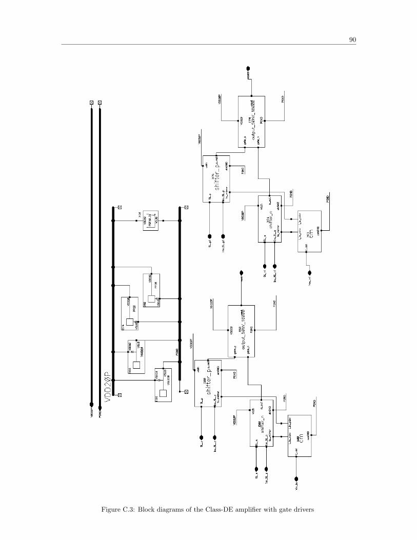
90
Figure C.3: Block diagrams of the Class-DE amplifier with gate drivers

Appendix D
Layout View
The layout views used in Virtuoso.

92
Figure D.1: Layout of the 10-bit-comparator

93
Figure D.2: Layout of the 10-bit-counter
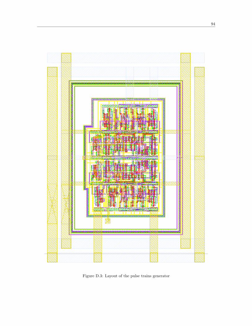
94
Figure D.3: Layout of the pulse trains generator

95
Figure D.4: Layout of the 30-bit-register

96
Figure D.5: Layout of the NMOS’s gate driver that designed by Wai Wong
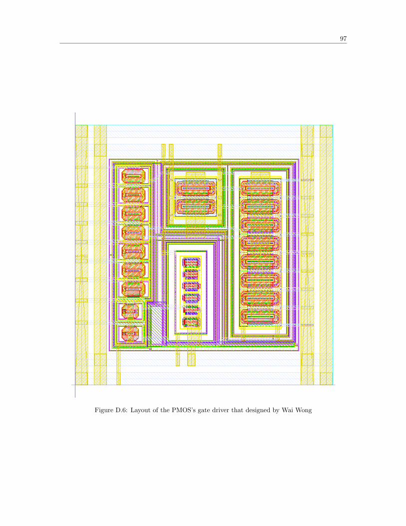
97
Figure D.6: Layout of the PMOS’s gate driver that designed by Wai Wong

98
Figure D.7: Layout of the gate drivers’ current mirror that designed by Wai Wong

99
Figure D.8: Layout of a branch of Class-DE amplifier that designed by Wai Wong

100
Figure D.9: Layout of the additional safety logic block that designed by Wai Wong

Bibliography
[1] W. Wong, C. Christoffersen, Samuel Pichardo, Laura Curiel “An Integrated Ultrasound Trans-
ducer Driver For HIFU Applications,” Proc. 2013 IEEE Canadian Conf. on Electrical and Com-
puter Engineering, 2013, pp. 1–5.
[2] W. Wong, “An Integrated Ultrasound Transducer Driver For HIFU Applications,” MSc Thesis
Dissertation, Lakehead University, 2013.
[3] “IEEE Standard Definitions and Methods of Measurement for Piezoelectric Vibrators,” IEEE
Std No.177, p. 1, 1966.
[4] J. L. Kivinen, “A Device for Performing Sonoporation on Adherent Cell Cultures”.MSc Thesis
Dissertation, Lakehead University, 2014.
[5] C. Christoffersen, W. Wong, S. Pichardo, G. Togtema and L. Curiel “Class-DE Ultrasound
Transducer Driver for HIFU Therapy” IEEE Transactions On Biomedical Circuits And Sys-
tems,vol.10, issue 2, pp.375-382, May 2015
[6] M. Kazimierczuk, “Class DE RF Power Amplifier,” in RF Power Amplifiers, Chichester, West
Sussex, U.K., Wiley, 2008, pp. 251–265.
[7] S. C. Tang and G. Clement, “A harmonic cancellation technique for an ultrasound transducer
excited by a switched-mode power converter,” IEEE Trans. on Ultrasonics, Ferroelectrics and
Frequency Control, vol. 55, no. 2, pp. 359–367, February 2008.
[8] L. Svilainis, V. Dumbrava and G. Motiejunas, “Optimization of the ultrasonic excitation stage”,
30th International Conference on Information Technology Interfaces, 2008. ITI 2008. 2008. pp.
791–796.
[9] T. Hall and C. Cain, “A Low Cost Compact 512 Channel Therapeutic Ultrasound System For
Transcutaneous Ultrasound Surgery,” AIP Conf. Proc., vol. 829, pp. 445–449, May 8 2006.

BIBLIOGRAPHY 102
[10] L. Yang, L. Xu, T. Yang and B. Zhang,“Class D power amplifier for audio beam system,”
International Conference on Mechatronics and Automation, 2007. ICMA 2007. 2007. pp. 3469–
3474.
[11] D. Zhao; M. T. Tan; H. K. Cha; J. Qu; Y. Mei; H. Yu; A. Basu; M. Je,“ High-voltage pulser
for ultrasound medical imaging applications”Integrated Circuits (ISIC), 2011 13th International
Symposium pp.408-411, 2011.
[12] A. Bozkurt; O. Farhanieh; R. B. Roy; A. S. Ergun, “ Design of a driver IC for an ultrasound
catheter ablation system” Ultrasonics Symposium (IUS), 2014 IEEE International, pp.1536-
1539, 2014
[13] K. Moro; J. Okada; K. Takada; S. Yoshizawa; S. i. Umemura,“Staircase-wave drive circuit to
drive therapeutic array transducer” Ultrasonics Symposium (IUS) IEEE, pp. 1799-1802, 2010
[14] D. C. Hamill, “Impedance plane analysis of class DE amplifier,” Electronics Letters, Vol. 30,
Issue 23, pp. 1905–1906, Nov. 1994.
[15] Samuel Pichardo, Rafael R. C. Silva ,Oleg Rubel, Laura Curiel “Efficient Driving of Piezoelec-
tric Transducers Using a Biaxial Driving Technique” PLOS ONE, DOI: 10.1371/journal. pone.
0139178, September 29, 2015
[16] H. Ballan and M. Declercq, “High-Voltage Analog and Digital Output Interfaces,” in, High
Voltage Devices and Circuits in Standard CMOS Technologies, Dordrecht, Netherlands: Kluwer
Academic Publishers, 1999, ch. 6, pp. 181-207.
[17] Yan Shi and Wang Hong ,“Synchronous Logical Circuits,” in The fundamental of digital circuit
Beijing, China: Higher Education Press, 2010, ch. 6, pp. 259-354
[18] “Foundry Design Kit 0.8 m 5/20V CMOS Cell Library”, Dalsa Semiconductor Inc., Document
No. DK08EDS01.04, 2005. 34 D. Clein 1958-, CMOS IC Layout : Concepts, Methodologies, and
Tools /. Boston : Newnes, c2000.