2.5d and 3d tsv products - ieee entity web · pdf file2.5d and 3d tsv products phil marcoux...
TRANSCRIPT

IEEE SCV Chapter, Components, Packaging and Manufacturing Technology Society
May 26, 2011
www.cpmt.org/scv
PPM Associates, Mtn View, CASemiconductor Intellectual Property [email protected]
10/26/2011 1PPM Associates, Mtn View, CASemiconductor Intellectual Property [email protected]
2.5D and 3D TSV Products
Phil MarcouxPPM Associates
Mountain View CAMay 2011
©PPM Associates 2011
PPM Associates, Mtn View, CASemiconductor Intellectual Property [email protected]
Outline
• Why 2.5D and 3D Products?
• Why TSVs?
• 2.5D/3D Product Examples
©PPM Associates 2011
IEEE SCV Chapter, Components, Packaging and Manufacturing Technology Society
May 26, 2011
www.cpmt.org/scv
PPM Associates, Mtn View, CASemiconductor Intellectual Property [email protected]
Acknowledgements
I am very appreciative of the assistance I received from the following for this presentation:
Sergey Savastiouk, ALLVIA
Jim Hewlett, ALLVIA
Javier De La Gruz, eSilicon
©PPM Associates 2011
PPM Associates, Mtn View, CASemiconductor Intellectual Property [email protected]
Why 3D and 2.5D?
To Meet the 3 “Givens” of Semiconductor Packaging
• Smaller– We are back to thinking of apartment buildings vs.
suburban sprawl. (remember MCMs?)
• Faster – Shorter signal distances = less obstacles.
• Cheaper– Stuff more into one rather than several packages.
– Better yields from chip partitioning
©PPM Associates 2011

IEEE SCV Chapter, Components, Packaging and Manufacturing Technology Society
May 26, 2011
www.cpmt.org/scv
PPM Associates, Mtn View, CASemiconductor Intellectual Property [email protected]
And 2.5D
PPM Associates, Mtn View, CASemiconductor Intellectual Property [email protected]
Source:

IEEE SCV Chapter, Components, Packaging and Manufacturing Technology Society
May 26, 2011
www.cpmt.org/scv
PPM Associates, Mtn View, CASemiconductor Intellectual Property [email protected]
10/26/2011 7PPM Associates, Mtn View, CASemiconductor Intellectual Property [email protected]
A 3D Product Example3D is the stacked assembly of chips upon each other without the benefit
of an interposer. 2.5D uses an interposer.
Source: CTI Leti/ST Micro
A two-die stack mixing advanced node technology (45nm) with mature node technology (130nm).
©PPM Associates 2011
PPM Associates, Mtn View, CASemiconductor Intellectual Property [email protected]
10/26/2011 8PPM Associates, Mtn View, CASemiconductor Intellectual Property [email protected]
TSVs and 3DReady for Primetime?
Factor TSV in IC TSV in Interposer
Area Impact Huge – Keep Out Areas Required
Low
Impact on IC performance
Large if the TSVs are too close to circuits
None
Cost Very High Low to Medium Depending on the type of TSV
Infrastructure Impact Huge – Co-Design is an absolute must!
Less or Not Required
©PPM Associates 2011

IEEE SCV Chapter, Components, Packaging and Manufacturing Technology Society
May 26, 2011
www.cpmt.org/scv
PPM Associates, Mtn View, CASemiconductor Intellectual Property [email protected]
10/26/2011 9PPM Associates, Mtn View, CASemiconductor Intellectual Property [email protected]
Some Non-TSV 3D Products3D is does not automatically mean TSVs – Wirebonds still are dominate
Stack of NAND Die
Source:
Cadence
PPM Associates, Mtn View, CASemiconductor Intellectual Property [email protected]
10/26/2011 10PPM Associates, Mtn View, CASemiconductor Intellectual Property [email protected]
Some Non-TSV 3D Products3D is the stacked assembly of chips upon each other without the benefit
of an interposer. 2.5D uses an interposer.
Source: Vertical Circuits, Inc.
A n 8 die memory stack using VCI’s
“VIP” (Vertical Interconnect Pillar)
IEEE SCV Chapter, Components, Packaging and Manufacturing Technology Society
May 26, 2011
www.cpmt.org/scv
PPM Associates, Mtn View, CASemiconductor Intellectual Property [email protected]
10/26/2011 11PPM Associates, Mtn View, CASemiconductor Intellectual Property [email protected]
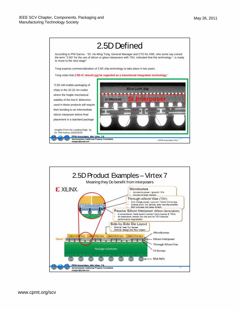
2.5D DefinedAccording to Phil Garrou - “Dr. Ho-Ming Tong, General Manager and CTO for ASE, who some say coined the term "2.5D" for the use of silicon or glass interposers with TSV, indicated that this technology “..is ready to move to the next stage”
Tong expects commercialization of 2.5D chip technology to take place in two years.
Tong notes that 2.5D IC should not be regarded as a transitional integration technology.”
Si Interposer
“2.5D will enable packaging of
chips in the 32-22 nm nodes
where the fragile mechanical
stability of the low-K dielectrics
used in these products will require
their bonding to an intermediate
silicon interposer before final
placement in a standard package
Insights From the Leading Edge by Dr. Phil Garrou 10/02/2010
©PPM Associates 2011
PPM Associates, Mtn View, CASemiconductor Intellectual Property [email protected]
10/26/2011 12PPM Associates, Mtn View, CASemiconductor Intellectual Property [email protected]
2.5D Product Examples – Virtex 7Meaning they Do benefit from interposers
IEEE SCV Chapter, Components, Packaging and Manufacturing Technology Society
May 26, 2011
www.cpmt.org/scv
PPM Associates, Mtn View, CASemiconductor Intellectual Property [email protected]
PPM Associates, Mtn View, CASemiconductor Intellectual Property [email protected]
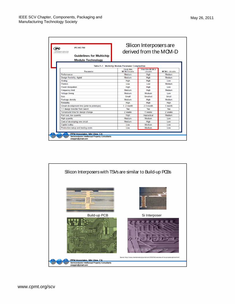
Silicon Interposers are derived from the MCM-D
PPM Associates, Mtn View, CASemiconductor Intellectual Property [email protected]
PPM Associates, Mtn View, CASemiconductor Intellectual Property [email protected]
Silicon Interposers with TSVs are similar to Build-up PCBs
Source: http://www.memsinvestorjournal.com/2010/04/overview-of-tsv-process-options.html
Build-up PCB Si Interposer

IEEE SCV Chapter, Components, Packaging and Manufacturing Technology Society
May 26, 2011
www.cpmt.org/scv
PPM Associates, Mtn View, CASemiconductor Intellectual Property [email protected]
VIA Types – in PCBs
©PPM Associates 2011
PPM Associates, Mtn View, CASemiconductor Intellectual Property [email protected]
VIA Types – in Silicon InterposersSurprise! – There’s more than you think.
©PPM Associates 2011

IEEE SCV Chapter, Components, Packaging and Manufacturing Technology Society
May 26, 2011
www.cpmt.org/scv
PPM Associates, Mtn View, CASemiconductor Intellectual Property [email protected]
VIA Types – for Silicon Interposers
Conformal Wet Etch – Large Area, Difficult to Control, Least Expensive
Conformal DRIE Etch – Smaller Area, Controlled Etch, Slightly More Expensive
Conformal Tented– Small Area, Difficult to Control, More Expensive due to polymer cost
Conformal Plugged– Small Area, Challenge to Plug, More Expensive due to polymer and plug cost
Filled Via– Small Area, Plating is long and difficult to Control, Higher Stress, Most Expensive
©PPM Associates 2011
PPM Associates, Mtn View, CASemiconductor Intellectual Property [email protected]
10/26/2011 18PPM Associates, Mtn View, CASemiconductor Intellectual Property [email protected]
2.5D Product Examples – Virtex 7Meaning they Do benefit from interposers

IEEE SCV Chapter, Components, Packaging and Manufacturing Technology Society
May 26, 2011
www.cpmt.org/scv
PPM Associates, Mtn View, CASemiconductor Intellectual Property [email protected]
10/26/2011 19PPM Associates, Mtn View, CASemiconductor Intellectual Property [email protected]
2.5D Product ExamplesAnalysis of the new Xilinx Virtex7. The graph shows the costs of various options considering tested and yielded silicon, the package laminate and assembly. It shows the benefit of having taken a large piece of silicon and partitioning it into 4 smaller die. In the baseline option, the silicon grossly dominates the cost of the device, followed by the cost of the laminate and the assembly. The 2.5D option shows the incremental cost of the silicon interposer and a much lower cost of the four smaller die. This is a strong case for the yield impact of large die. It’s estimated that the yielded cost of the 2.5D assembly is about half that of the current monolithic solution.
Source: JDlC, eSilicon
PPM Associates, Mtn View, CASemiconductor Intellectual Property [email protected]
10/26/2011 20PPM Associates, Mtn View, CASemiconductor Intellectual Property [email protected]
Source: W. T. Bottoms 3MTS
Possible Network Processor

IEEE SCV Chapter, Components, Packaging and Manufacturing Technology Society
May 26, 2011
www.cpmt.org/scv
PPM Associates, Mtn View, CASemiconductor Intellectual Property [email protected]
10/26/2011 21PPM Associates, Mtn View, CASemiconductor Intellectual Property [email protected]
2.5D Product ExamplesNetwork Processor – This example includes memory in the die. The baseline die has 110Mb of 6T SRAM. Die size increased to the point that the yield impact became significant. The 2.5D solution removed the internal SRAM and included a 2Gb DRAM adjacent to the die. This large amount of memory along with the 2.5D Silicon interposer still proved to be 15% less expensive than the monolithic solution when you only consider the items shown in the legend.
Source: JDlC, eSilicon
PPM Associates, Mtn View, CASemiconductor Intellectual Property [email protected]
10/26/2011 22PPM Associates, Mtn View, CASemiconductor Intellectual Property [email protected]
2.5D Interposer Specs
Today In ~ 5 years Possibly > 5 years
Substrate Mtl. Silicon Silicon Silicon or Glass
Size 200mm 300mm > 300mm
Thickness 300 – 400um 300 – 400um 200 – 300um
Via Diameter 60 to 80um 40 to 60um <40um
Aspect Ratios 5 to 1 Range of 5 - 10 to 1 Range of 5 - 10 to 1
Plating Conformal or Filled
Cu
Conformal or Filled
Cu
Conformal or Filled
Cu
Insulator Oxide or Poly Oxide or Poly Oxide or Poly or
NONE
RDLs 1 to 2 2 to 3 >3
©PPM Associates 2011

IEEE SCV Chapter, Components, Packaging and Manufacturing Technology Society
May 26, 2011
www.cpmt.org/scv
PPM Associates, Mtn View, CASemiconductor Intellectual Property [email protected]
There’s Too Many Flavors and Options!
In every transition in technology we suffer a period of
Too Many Options
• Wirebond
• FlipChip – Solder
• Flipchip – Conductive Epoxy
• Flipchip – Copper Pillar
• Wraparound WLP
• Stud Bumping
• Conformal TSV
• Filled TSV
PPM Associates, Mtn View, CASemiconductor Intellectual Property [email protected]
Conclusion
• 3D and 2.5D is an exciting extension to the IC packaging world.
• The roots are with the MCMs of the early ‘90s
• Which means demons like lack of KGD still lurk
• Too many options exist and the infrastructure still needs growth
• Interposers (2.5D) aren’t just a stepping stone to 3D
©PPM Associates 2011