25th anniversary article. cvd polymers. a new paradigm for surface modifi cation and device...
TRANSCRIPT

5392
REV
IEW
www.advmat.de
25th Anniversary Article: CVD Polymers: A New Paradigm for Surface Modifi cation and Device Fabrication
Anna Maria Coclite , Rachel M. Howden , David C. Borrelli , Christy D. Petruczok , Rong Yang , Jose Luis Yagüe , Asli Ugur , Nan Chen , Sunghwan Lee , Won Jun Jo , Andong Liu , Xiaoxue Wang , and Karen K. Gleason *
Well-adhered, conformal, thin (<100 nm) coatings can easily be obtained by chemical vapor deposition (CVD) for a variety of technological applications. Room temperature modifi cation with functional polymers can be achieved on virtually any substrate: organic, inorganic, rigid, fl exible, planar, three-dimen-sional, dense, or porous. In CVD polymerization, the monomer(s) are deliv-ered to the surface through the vapor phase and then undergo simultaneous polymerization and thin fi lm formation. By eliminating the need to dissolve macromolecules, CVD enables insoluble polymers to be coated and prevents solvent damage to the substrate. CVD fi lm growth proceeds from the substrate up, allowing for interfacial engineering, real-time monitoring, and thickness control. Initiated-CVD shows successful results in terms of rationally designed micro- and nanoengineered materials to control molecular interactions at material surfaces. The success of oxidative-CVD is mainly demonstrated for the deposition of organic conducting and semiconducting polymers.
1 . Introduction
Chemical vapor deposition (CVD) is a powerful technology for engineering surfaces and is typically the method of choice for growing high quality inorganic layers. More recently, CVD methods have been invented which fully retain the rich chem-istry of organic monomers. [ 1,2 ] The solvent-free deposition of robust thin fi lms with high densities of organic functional groups is an enabling technology for surface modifi cation of, but not limited to, industrial parts, membranes, microfl uidic structures, and biomedical devices. In analogy to their inor-ganic counterparts, CVD polymeric layers can be integrated into device fabrication schemes for optoelectronics and sen-sors. The desirable attributes of CVD polymers include surface
© 2013 WILEY-VCH Verlag GmbH & Co. KGaA, Weinhewileyonlinelibrary.com
Prof. A. M. Coclite Institute of Solid State Physics Graz University of Technology Graz, 8010 , Austria Dr. R. Howden, D. C. Borrelli, C. D. Petruczok, R. Yang, Dr. J. L. Yagüe, Dr. A. Ugur, Dr. N. Chen, Dr. S. Lee, W. J. Jo, A. Liu, X. Wang, Prof. K. K. Gleason Department of Chemical Engineering Massachusetts Institute of Technology Cambridge, MA 02139 , USA E-mail: [email protected]
DOI: 10.1002/adma.201301878
energy modifi cation, environmental pro-tection, mechanical fl exibility, conformal coverage, and/or chemical and biological specifi city.
CVD expands the application space for polymeric surface modifi cation. Vapor deposition is ideally suited for synthe-sizing thin fi lms of polymers that are insoluble or infusible. Indeed, fl uoro-polymers, crosslinked organic materials, and conjugated polymers are three of the most studied categories of CVD polymer fi lms. Additionally, solvent-free processing avoids potential swelling or dissolution of the substrate.
By building the polymeric thin fi lms from the surface up, strategic use of inter-facial modifi cation enables covalent chem-ical bonds to form between the CVD pol-ymer fi lm and substrate. The interfacial
grafting results in surface layers, which are robustly adhered to the underlying substrate. CVD provides precise control over fi lm thickness and also yields so-called “conformal coatings”, which uniformly cover complex geometric features, including trenches, microparticles, and nanotubes. [ 3–5 ]
Synthesis from vapor phase monomers (also referred in the text as gas phase monomers) obviates the need to remove entrained solvents using a curing step. Lack of residual solvent is favorable for achieving biocompatibility. [ 6 ] Further reductions in impurity levels can be achieved through the purifi cation of the low molecular weight monomers before their use as reac-tants in the CVD polymerization process. Optoelectronic device performance and stability typically improve as impurity levels decrease.
In contrast to solution synthesis methods, the monomeric reactants for CVD do not need to be soluble. However, the monomeric species must be volatile. Vapor phase processes can be classifi ed depending on the deposition mechanism: chain growth (e.g., plasma enhanced chemical vapor deposition, PECVD [ 7,8 ] ) and step growth polymerization (e.g., vapor deposi-tion polymerization, VDP [ 9 ] or CVD grown parylene [ 6,10 ] ). Chain growth and step growth mechanisms have been demonstrated also for initiated CVD (iCVD) and oxidative CVD (oCVD), respectively. The focus of this review will be mainly on the latter two techniques (iCVD and oCVD) to highlight the suc-cessful implementation of these techniques in many techno-logical fi elds. The characteristics of iCVD polymers have been
im Adv. Mater. 2013, 25, 5392–5423
REV
IEW
www.advmat.de
Prof. Karen K. Gleason is the Alexander and I. Michael Kasser Professor of Chemical Engineering at MIT. The coauthors are members of her lab: Drs. Anna Maria Coclite, Jose Luis Yagüe, Asli Ugur, Nan Chen, Sunghwan Lee are postdoctoral associates, David Borrelli, Christy D. Petruczok, Rong Yang, Won Jun Jo, Andong Liu, Xiaoxue Wang are currently doctoral candidates; Rachel M. Howden received her PhD in 2013. From left to right: R.Y., A.L., C.D.P., N.C., J.L.Y., R.M.H., A.U., S.L., D.B., W.J.J., X.W., K.K.G., Y.U. and A.M.C.
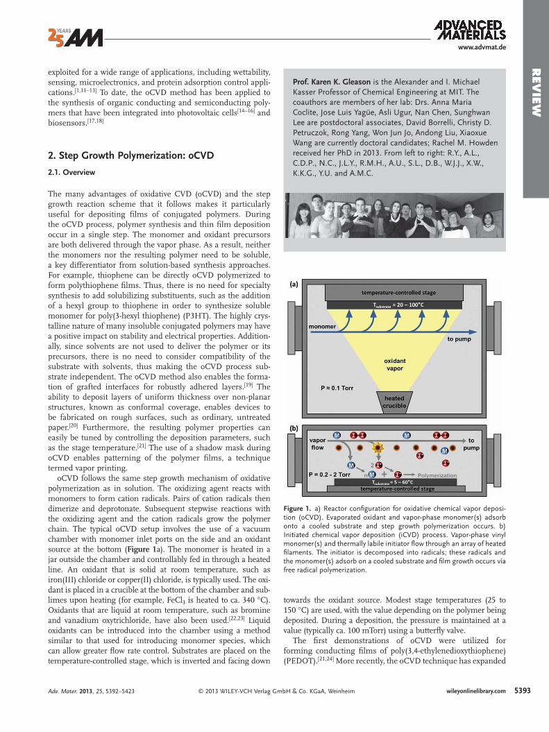
Figure 1. a) Reactor confi guration for oxidative chemical vapor deposi-tion (oCVD). Evaporated oxidant and vapor-phase monomer(s) adsorb onto a cooled substrate and step growth polymerization occurs. b) Initiated chemical vapor deposition (iCVD) process. Vapor-phase vinyl monomer(s) and thermally labile initiator fl ow through an array of heated fi laments. The initiator is decomposed into radicals; these radicals and the monomer(s) adsorb on a cooled substrate and fi lm growth occurs via free radical polymerization.
exploited for a wide range of applications, including wettability, sensing, microelectronics, and protein adsorption control appli-cations. [ 1,11–13 ] To date, the oCVD method has been applied to the synthesis of organic conducting and semiconducting poly-mers that have been integrated into photovoltaic cells [ 14–16 ] and biosensors. [ 17,18 ]
2 . Step Growth Polymerization: oCVD
2.1 . Overview
The many advantages of oxidative CVD (oCVD) and the step growth reaction scheme that it follows makes it particularly useful for depositing fi lms of conjugated polymers. During the oCVD process, polymer synthesis and thin fi lm deposition occur in a single step. The monomer and oxidant precursors are both delivered through the vapor phase. As a result, neither the monomers nor the resulting polymer need to be soluble, a key differentiator from solution-based synthesis approaches. For example, thiophene can be directly oCVD polymerized to form polythiophene fi lms. Thus, there is no need for specialty synthesis to add solubilizing substituents, such as the addition of a hexyl group to thiophene in order to synthesize soluble monomer for poly(3-hexyl thiophene) (P3HT). The highly crys-talline nature of many insoluble conjugated polymers may have a positive impact on stability and electrical properties. Addition-ally, since solvents are not used to deliver the polymer or its precursors, there is no need to consider compatibility of the substrate with solvents, thus making the oCVD process sub-strate independent. The oCVD method also enables the forma-tion of grafted interfaces for robustly adhered layers. [ 19 ] The ability to deposit layers of uniform thickness over non-planar structures, known as conformal coverage, enables devices to be fabricated on rough surfaces, such as ordinary, untreated paper. [ 20 ] Furthermore, the resulting polymer properties can easily be tuned by controlling the deposition parameters, such as the stage temperature. [ 21 ] The use of a shadow mask during oCVD enables patterning of the polymer fi lms, a technique termed vapor printing.
oCVD follows the same step growth mechanism of oxidative polymerization as in solution. The oxidizing agent reacts with monomers to form cation radicals. Pairs of cation radicals then dimerize and deprotonate. Subsequent stepwise reactions with the oxidizing agent and the cation radicals grow the polymer chain. The typical oCVD setup involves the use of a vacuum chamber with monomer inlet ports on the side and an oxidant source at the bottom ( Figure 1 a). The monomer is heated in a jar outside the chamber and controllably fed in through a heated line. An oxidant that is solid at room temperature, such as iron(III) chloride or copper(II) chloride, is typically used. The oxi-dant is placed in a crucible at the bottom of the chamber and sub-limes upon heating (for example, FeCl 3 is heated to ca. 340 °C). Oxidants that are liquid at room temperature, such as bromine and vanadium oxytrichloride, have also been used. [ 22,23 ] Liquid oxidants can be introduced into the chamber using a method similar to that used for introducing monomer species, which can allow greater fl ow rate control. Substrates are placed on the temperature-controlled stage, which is inverted and facing down
© 2013 WILEY-VCH Verlag GAdv. Mater. 2013, 25, 5392–5423
towards the oxidant source. Modest stage temperatures (25 to 150 °C) are used, with the value depending on the polymer being deposited. During a deposition, the pressure is maintained at a value (typically ca. 100 mTorr) using a butterfl y valve.
The fi rst demonstrations of oCVD were utilized for forming conducting fi lms of poly(3,4-ethylenedioxythiophene) (PEDOT). [ 21,24 ] More recently, the oCVD technique has expanded
5393wileyonlinelibrary.commbH & Co. KGaA, Weinheim

5394
REV
IEW
www.advmat.de
to the deposition of other conjugated polymers, including semi-conducting layers and functionalizable conducting copolymers. To date, these oCVD polymers have been applied to fulfi ll var-ious roles in organic photovoltaics, electrochromic devices, and sensors. A comprehensive review of oCVD and other methods for the vapor deposition of conjugated polymers and their appli-cations has recently been published. [ 25 ]
2.2 . Substrate Independence
The low deposition temperatures (ca. 20–150 °C) enable oCVD polymers to be directly deposited on a wide range of substrates, including paper and plastic, without fear of thermal degrada-tion. Additionally, the oCVD requires no specifi c process opti-mization for application to different types of materials. This benefi t derives from avoiding surface tension driven phe-nomena, which lead to dewetting, blanketing, air gap forma-tion, sidewall thinning, and formation of menisci.
The work of Park et al. demonstrates the compatibility of the oCVD process with graphene substrates. [ 26 ] The graphene was simply exposed to a vaporized mixture EDOT monomer and the FeCl 3 oxidizing agent to form the oCVD polymer layer. The moderate deposition conditions resulted in the direct deposition of a pure PEDOT hole transport layer without damage to the gra-
Figure 2. Images of oCVD PEDOT along the top are compared with those of spin-cast PEDOT:PSS along the bottom. On graphene (a,b), the optical micrographs and the inset photo-graphs, show that the dewetting defects present in PEDOT:PSS are absent in the oCVD coating. On imprinted PMMA features, the scanning electron micrographs show complete infi lling of by oCVD whiles voids are left by spin-casting (c,d), and constant thickness of the conformal coating by oCVD as opposed to the variation in coating thickness observed for PEDOT:PSS (e,f). On poly (acrylonitrile) fi ber mats, the conformal oCVD fi lm, encases each fi ber, while dewetting of the PEDOT:PSS forms agglomates (g,h). Photographs show the oCVD coating is uniform over rice paper, while spin-coating damages this substrate. a,b) Reproduced with per-mission. [ 26 ] Copyright 2012, American Chemical Society. c–f) Reproduced with permission. [ 27 ] Copyright 2013, Elsevier. g,h) Reproduced with permission. [ 28 ] Copyright 2008, Wiley. i,j) Repro-duced with permission. [ 15 ] Copyright 2011, Wiley.
phene electrode. When integrated into solar cells, the resulting power conversion effi -ciency was ca. 94% of the ITO control device. Figure 2 a and 2 b compare quartz/graphene substrates coated by oCVD and spin-cast PEDOT:PSS, respectively. In the latter, irregu-larly shaped dewetting defects are observed, which appear as multiple dark spots to the human eye. In contrast, the oCVD PEDOT surface is defect-free over the entire area.
Vapor phase reactants are able to diffuse into complex micro- and nano- structured surfaces. Such 3D surface architectures are desired to enhance light absorption in organic photovoltaic devices, where the exciton dif-fusion length limits active layer thicknesses. Howden et al. showed that oCVD PEDOT is compatible with wide range of nano- to macro-scale textured surfaces, [ 29 ] enhancing the light absorption (light trapping) in photovoltaic structures. Figure 2 c shows the ability of the oCVD PEDOT to precisely follow the geom-etry the interface. In contrast, voids form when solution-processed PEDOT:PSS (Figure 2 d) is applied to a similar nanostructured sur-face. The conformal nature oCVD PEDOT is again demonstrated over a nanowedge pattern (Figure 2 e), where an ultrathin layer thick-ness of ca. 9 nm covers all portions of the features. In contrast, spin-coated PEDOT:PSS (Figure 2 f) wells up in the bottoms of the fea-tures, while thinning at the tops.
The oCVD method is able to penetrate and coat the inner surfaces of porous media,
wileyonlinelibrary.com © 2013 WILEY-VCH Verlag G
such as foams and membranes. Subsequent dissolution of the membrane leaves behind the oCVD templated features. In the case of membranes with cylindrical pores, nanotubes of conju-gated polymers are formed.
When applied to fi ber-base substrates, such as paper, electro-spun nanofi ber mats, or textiles, the oCVD conjugated polymers completely surrounds each fi ber. [ 30 ] Poly(acrylonitrile) fi ber mats conformally coated with oCVD PEDOT (Figure 2 g) create a high surface area platform for resistance-based sensing. [ 31 ] In con-trast, agglomeration occurs in the fi brous substrate after solu-tion application of PEDOT:PSS (Figure 2 h). In Figure 2 i, the oCVD PEDOT leaves the rice paper substrate undamaged, while the PEDOT:PSS solution degrades this substrate (Figure 2 j).
Conformal coating of carbon nanotubes (CNTs) by oCVD PEDOT ca. 6 nm thick was demonstrated by Vaddiraju et al. [ 32 ] By lowering the activation energy required for creation of mobile carriers, an enhancement in radial conductivity was obtained. This approach can be used to create many functional materials and devices.
2.3 . Grafting and Patterning
The vapor phase delivery of oxidants in oCVD builds the fi lm from the surface up and permits covalent bonds to form at the
mbH & Co. KGaA, Weinheim Adv. Mater. 2013, 25, 5392–5423
REV
IEW
www.advmat.de
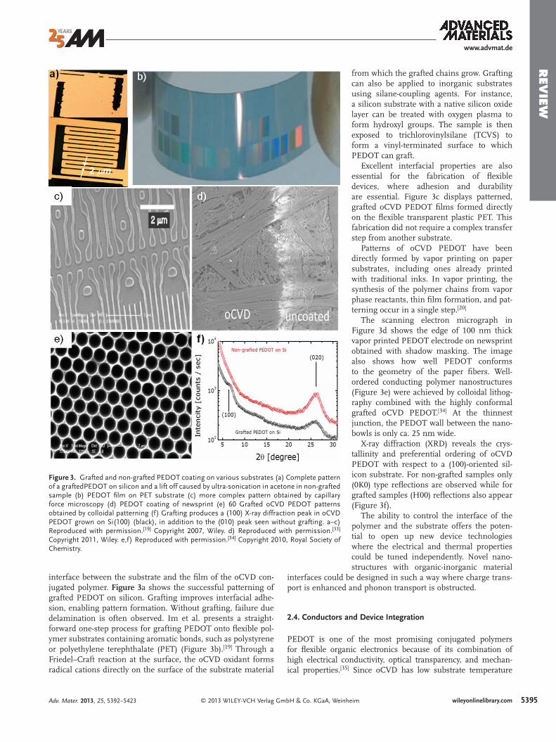
Figure 3. Grafted and non-grafted PEDOT coating on various substrates (a) Complete pattern of a graftedPEDOT on silicon and a lift off caused by ultra-sonication in acetone in non-grafted sample (b) PEDOT fi lm on PET substrate (c) more complex pattern obtained by capillary force microscopy (d) PEDOT coating of newsprint (e) 60 Grafted oCVD PEDOT patterns obtained by colloidal patterning (f) Grafting produces a (100) X-ray diffraction peak in oCVD PEDOT grown on Si(100) (black), in addition to the (010) peak seen without grafting. a–c) Reproduced with permission. [ 19 ] Copyright 2007, Wiley. d) Reproduced with permission. [ 33 ] Copyright 2011, Wiley. e,f) Reproduced with permission. [ 34 ] Copyright 2010, Royal Society of Chemistry.
interface between the substrate and the fi lm of the oCVD con-jugated polymer. Figure 3 a shows the successful patterning of grafted PEDOT on silicon. Grafting improves interfacial adhe-sion, enabling pattern formation. Without grafting, failure due delamination is often observed. Im et al. presents a straight-forward one-step process for grafting PEDOT onto fl exible pol-ymer substrates containing aromatic bonds, such as polystyrene or polyethylene terephthalate (PET) (Figure 3 b). [ 19 ] Through a Friedel–Craft reaction at the surface, the oCVD oxidant forms radical cations directly on the surface of the substrate material
© 2013 WILEY-VCH Verlag GmbH & Co. KGaA, WeinAdv. Mater. 2013, 25, 5392–5423
from which the grafted chains grow. Grafting can also be applied to inorganic substrates using silane-coupling agents. For instance, a silicon substrate with a native silicon oxide layer can be treated with oxygen plasma to form hydroxyl groups. The sample is then exposed to trichlorovinylsilane (TCVS) to form a vinyl-terminated surface to which PEDOT can graft.
Excellent interfacial properties are also essential for the fabrication of fl exible devices, where adhesion and durability are essential. Figure 3 c displays patterned, grafted oCVD PEDOT fi lms formed directly on the fl exible transparent plastic PET. This fabrication did not require a complex transfer step from another substrate.
Patterns of oCVD PEDOT have been directly formed by vapor printing on paper substrates, including ones already printed with traditional inks. In vapor printing, the synthesis of the polymer chains from vapor phase reactants, thin fi lm formation, and pat-terning occur in a single step. [ 20 ]
The scanning electron micrograph in Figure 3 d shows the edge of 100 nm thick vapor printed PEDOT electrode on newsprint obtained with shadow masking. The image also shows how well PEDOT conforms to the geometry of the paper fi bers. Well-ordered conducting polymer nanostructures (Figure 3 e) were achieved by colloidal lithog-raphy combined with the highly conformal grafted oCVD PEDOT. [ 34 ] At the thinnest junction, the PEDOT wall between the nano-bowls is only ca. 25 nm wide.
X-ray diffraction (XRD) reveals the crys-tallinity and preferential ordering of oCVD PEDOT with respect to a (100)-oriented sil-icon substrate. For non-grafted samples only (0K0) type refl ections are observed while for grafted samples (H00) refl ections also appear (Figure 3 f).
The ability to control the interface of the polymer and the substrate offers the poten-tial to open up new device technologies where the electrical and thermal properties could be tuned independently. Novel nano-structures with organic-inorganic material
interfaces could be designed in such a way where charge trans-port is enhanced and phonon transport is obstructed.
2.4 . Conductors and Device Integration
PEDOT is one of the most promising conjugated polymers for fl exible organic electronics because of its combination of high electrical conductivity, optical transparency, and mechan-ical properties. [ 35 ] Since oCVD has low substrate temperature
5395wileyonlinelibrary.comheim
5396
REV
IEW
www.advmat.de
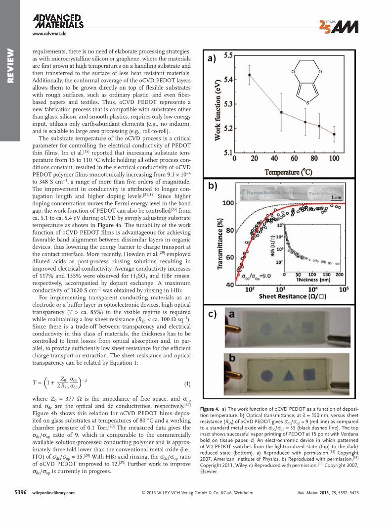
Figure 4. a) The work function of oCVD PEDOT as a function of deposi-tion temperature. b) Optical transmittance, at λ = 550 nm, versus sheet resistance ( R sh ) of oCVD PEDOT gives σ dc / σ op = 9 (red line) as compared to a standard metal oxide with σ dc / σ op = 35 (black dashed line). The top inset shows successful vapor printing of PEDOT at 15 point with Verdana bold on tissue paper. c) An electrochromic device in which patterned oCVD PEDOT switches from the light/oxidized state (top) to the dark/reduced state (bottom). a) Reproduced with permission. [ 35 ] Copyright 2007, American Institute of Physics. b) Reproduced with permission. [ 33 ] Copyright 2011, Wiley. c) Reproduced with permission. [ 36 ] Copyright 2007, Elsevier.
requirements, there is no need of elaborate processing strategies, as with microcrystalline silicon or graphene, where the materials are fi rst grown at high temperatures on a handling substrate and then transferred to the surface of less heat resistant materials. Additionally, the conformal coverage of the oCVD PEDOT layers allows them to be grown directly on top of fl exible substrates with rough surfaces, such as ordinary plastic, and even fi ber-based papers and textiles. Thus, oCVD PEDOT represents a new fabrication process that is compatible with substrates other than glass, silicon, and smooth plastics, requires only low-energy input, utilizes only earth-abundant elements (e.g., no indium), and is scalable to large area processing (e.g., roll-to-roll).
The substrate temperature of the oCVD process is a critical parameter for controlling the electrical conductivity of PEDOT thin fi lms. Im et al. [ 35 ] reported that increasing substrate tem-perature from 15 to 110 °C while holding all other process con-ditions constant, resulted in the electrical conductivity of oCVD PEDOT polymer fi lms monotonically increasing from 9.1 × 10 −4 to 348 S cm −1 , a range of more than fi ve orders of magnitude. The improvement in conductivity is attributed to longer con-jugation length and higher doping levels. [ 21,35 ] Since higher doping concentration moves the Fermi energy level in the band gap, the work function of PEDOT can also be controlled [ 35 ] from ca. 5.1 to ca. 5.4 eV during oCVD by simply adjusting substrate temperature as shown in Figure 4 a. The tunability of the work function of oCVD PEDOT fi lms is advantageous for achieving favorable band alignment between dissimilar layers in organic devices, thus lowering the energy barrier to charge transport at the contact interface. More recently, Howden et al. [ 29 ] employed diluted acids as post-process rinsing solutions resulting in improved electrical conductivity. Average conductivity increases of 117% and 135% were observed for H 2 SO 4 and HBr rinses, respectively, accompanied by dopant exchange. A maximum conductivity of 1620 S cm −1 was obtained by rinsing in HBr.
For implementing transparent conducting materials as an electrode or a buffer layer in optoelectronic devices, high optical transparency ( T > ca. 85%) in the visible regime is required while maintaining a low sheet resistance ( R sh < ca. 100 Ω sq −1 ). Since there is a trade-off between transparency and electrical conductivity in this class of materials, the thickness has to be controlled to limit losses from optical absorption and, in par-allel, to provide suffi ciently low sheet resistance for the effi cient charge transport or extraction. The sheet resistance and optical transparency can be related by Equation 1 :
T = 1 + Z0
2Rsh
Fop
Fdc)−2(
(1)
where Z 0 = 377 Ω is the impedance of free space, and σ op and σ dc are the optical and dc conductivities, respectively. [ 37 ] Figure 4 b shows this relation for oCVD PEDOT fi lms depos-ited on glass substrates at temperatures of 80 °C and a working chamber pressure of 0.1 Torr. [ 20 ] The measured data gives the σ dc / σ op ratio of 9, which is comparable to the commercially available solution-processed conducting polymer and is approx-imately three-fold lower than the conventional metal oxide (i.e., ITO) of σ dc / σ op ≈ 35. [ 20 ] With HBr acid rinsing, the σ dc / σ op ratio of oCVD PEDOT improved to 12. [ 29 ] Further work to improve σ dc / σ op is currently in progress.
wileyonlinelibrary.com © 2013 WILEY-VCH Verlag GmbH & Co. KGaA, Weinheim Adv. Mater. 2013, 25, 5392–5423

REV
IEW
www.advmat.de
Figure 5. a) Bottom-illuminated OPV with an oCVD PEDOT anode directly on PET retains performance with repeated 5 nm-radius fl exes. b) Top-illuminated OPV with 2.0% PCE having oCVD PEDOT as the fi nal layer fabricated on a postage stamp, representing a rough opaque sub-strate. (bottom). c) Monolithic integration of 250-cell arrays on tracing paper (top); vapor printed PEDOT anode pattern (bottom left); and a completed 7 cm × 7 cm capable of >50 V output (bottom right). d) Folding of oCVD PEDOT coated substrates (top). Increased absorption with the decreasing hinge angle of OPV half-cells fabricated using oCVD PEDOT (bottom). a,c) Reproduced with permission. [ 33 ] Copyright 2011, Wiley. b) Reproduced with permission. [ 38 ] Copyright 2012, Wiley. d) Reproduced with permission. [ 27 ] Copyright 2013, Elsevier
The color-transition properties exhibited by PEDOT have been investigated for electrochromic applications such as smart windows and light management devices. PEDOT displays a transparent light-blue color in the oxidized state and a dark-blue hue in the reduced state. When cycled between oxidized and reduced states, the electrochromic switching of a device fabricated by integrating patterned oCVD PEDOT onto ITO/glass substrates occurs, as can be seen in Figure 4 c [ 36 ] The dark-to-light transition occurs within ca. 10 s, while a light-to-dark switching requires approximately 1 min.
To demonstrate the utility of the direct fabrication of oCVD layers, PEDOT electrodes have been fabricated on a wide range of fl exible, foldable, and non-planar surfaces. The conductivity of oCVD PEDOT electrodes and the performance of full OPV devices with oCVD PEDOT remains unchanged after repeated mechanical deformation tests. In Figure 5 a, OPV devices with oCVD PEDOT electrodes on polyethylene terephthalate (PET) present no signifi cant change in performance over 100 com-pressive fl exing cycles. In contrast, the electrical conductivity of commercially available ITO on PET substrates deteriorates rapidly and cracks are visible after repeated fl exing via optical microscope. Flexibility is essential for implementation of roll-to-roll processing, desired for economical production.
While photovoltaic (PV) devices traditionally utilize illumina-tion through a transparent substrate like glass or plastic, strate-gies compatible with opaque substrates open up new potential avenues for the use of solar power. Top-illuminated inverted photovoltaic devices on opaque substrates were fabricated [ 38 ] using an oCVD PEDOT electrode deposited directly on top the rest of the cell stack (Figure 5 b). The oCVD PEDOT anode layer is directly deposited on the device stack without any damage to the underlying active layer materials by insertion of a thin buffer layer of molybdenum trioxide (MoO 3 ). [ 38,39 ] With this inverted device structure, top-illuminated OPV devices were demonstrated on a variety of common opaque substrates such as photo paper, magazine print, and plastic food packaging. Figure 5 b shows an OPV fabricated on a U.S stamp, having a power conversion effi ciency of 2.0%. [ 38 ]
Facile monolithic integration of devices into circuits is ena-bled on paper utilizing substrate-independent vapor-printed oCVD PEDOT electrodes. [ 20,26 ] This approach allows the fab-rication and cost-effective prototyping of fl exible and foldable organic devices by vapor printing on inexpensive everyday substrates including paper. Large-area PV prototype arrays have been vapor-printed directly on the unmodifi ed surface of fi brous papers, offer a thinner, lighter-weight alternative to plastic substrates (ca. 0.001 g cm −2 , <40 μ m thick). The paper PV arrays produce >50V and power common electronic displays in ambient indoor lighting, even after tortuous fl exing and folding. Figure 5 c (top) show a schematic of the process inte-gration fl ow for fabricating the bottom-illuminated PV device structures using a series of shadow masking steps. For the oCVD step, the mask itself is stencil cut from paper. The com-pleted circuit of individual cells, and printing patterns of each device layer and complete 250-cell series integrated monolithic arrays on tracing paper are shown in Figure 5 c (bottom). [ 20 ] This same strategy could be utilized to fabricate other types of optoelectronic devices, logic elements, energy storage devices as well as integrated circuits containing mixtures of these discrete devices.
© 2013 WILEY-VCH Verlag GAdv. Mater. 2013, 25, 5392–5423
Because oCVD PEDOT fi lms retain their conductivity upon folding, a variety of macro-scale non-planar 3D-structures can be created (Figure 5 d). [ 27 ] These architectures offer the possibility to improve the output power over a given area by more effi ciently
5397wileyonlinelibrary.commbH & Co. KGaA, Weinheim

539
REV
IEW
www.advmat.de
absorbing and converting the incident light while maintaining a fi xed active layer thickness for optimal exciton diffusion. For half-cells fabricated using oCVD PEDOT electrodes and DBP (tetraphenyldibenzoperifl anthene) absorber layers, increased absorption was measured as hinge angle decreased (Figure 5 d) for substrates folded into V-shaped confi gurations.
2.5 . oCVD Semiconductors
Semiconducting polymers are of great interest as active layer materials in organic electronic and optoelectronic devices,
8 wileyonlinelibrary.com © 2013 WILEY-VCH Verlag G
Figure 6. a) oCVD unsubstituted polythiophene (PT). (left) During the oCVtive fi lm. Dedoping the fi lm with some reducing agent, such as methanol,doped (blue) fi lm shows characteristic bipolaron peaks, whereas the semiBilayer heterojunction organic photovoltaic devices fabricated with oCVD PTfi gure shows the absorption spectra of oCVD PT and C 60 . b) Polyisothianatemperature of deposition is shown to control the resulting polymer propertability to easily pattern the oCVD polymer and the ability to conformally coadeposited by oCVD. (middle) Electrospun fi ber mats with fl uorescently labepoly(EDOT- co -3TE). Attached to the avidin are biotin labeled with red quamat exposed to biotin solutions of 5 nM (blue), 50 nM (purple), 500 nM (gCopyright 2012, Elsevier. b) Reproduced with permission. [ 44 ] Copyright 20132012, Royal Society of Chemistry. d) Reproduced with permission. [ 46 ] Copyr
such as organic photovoltaics (OPVs), [ 40 ] organic light emitting diodes, [ 41 ] and organic fi eld effect transistors. [ 42 ] Researchers have recently employed oCVD for the deposition of several semiconducting polymers. Unsubstituted polythiophene (PT), which is insoluble and typically diffi cult to process, was easily prepared by oCVD. Using iron(III) chloride as the oxidizing agent, the as-deposited oCVD PT fi lms were blue in appear-ance. [ 43 ] ( Figure 6 a) Excess oxidizing agent present during the oCVD process doped the fi lms, resulting in conductivities up to 20 S/cm. Positions of the mid-gap absorption peaks (0.8 and 1.6 eV) in the doped fi lms demonstrate that the polymer fi lms are heavily doped and bipolarons are present (Figure 6 a,
mbH & Co. KGaA, Weinheim
D process, the polymer is overoxidized which results in a doped, conduc- results in a neutral polymer fi lm. (middle) The absorption spectra of the conducting (red) fi lm shows a characteristic π – π * transition peak. (right) and C 60 demonstrated power conversion effi ciencies up to 0.8%. The inset phthene fi lms prepared by oCVD at various temperatures. Controlling the ies. c) oCVD polyselenophene fi lms on paper substrates demonstrating the t rough substrates. d) Copolymers of EDOT and 3-thiopheneethanol (3TE) led avidin (green) attached to –OH functional groups of conformal oCVD
ntum dots. (right) Response of avidin/poly(EDOT- co -3TE) on electrospun reen), and 5 μ M (red) concentrations. a) Reproduced with permission. [ 43 ] , American Chemical Society. c) Reproduced with permission. [ 45 ] Copyright ight 2011, Wiley.
Adv. Mater. 2013, 25, 5392–5423
REV
IEW
www.advmat.de
middle). Reduction with methanol dedoped the polymer and resulted in neutral, red PT fi lms. Changes in the absorption spectra confi rmed the semiconducting nature of the rinsed PT fi lms (Figure 6 a, middle). Bilayer heterojunction organic solar cells were then fabricated using semiconducting oCVD PT as the electron donor. The oCVD PT was deposited directly onto ITO-glass substrates. Thermally evaporated C 60 was used as the electron acceptor layer, and a bathocuproine (BCP) exciton-blocking layer and silver top cathode were used. After opti-mizing layer thicknesses, power conversion effi ciencies up to 0.8% were obtained using 25 nm of PT and 30 nm of C 60 . To date, this remains the highest effi ciency solar cell that utilized a vapor-deposited donor polymer. The image in the far right of Figure 6 a shows the current density-voltage (JV) curve of the PT/C 60 devices.
Properties of oCVD semiconducting polymers are easily tuned by controlling the deposition parameters. A separate study of oCVD polythiophene demonstrated the use of vana-dium oxytrichloride (VOCl 3 ) as the oxidizing agent. [ 23 ] Since VOCl 3 is a volatile liquid, controlling its fl ow rate and the stage temperature allowed for control of the surface concentration of VOCl 3 on the stage in the reactor chamber. Thus, by con-trolling those parameters as well as the monomer fl ow rate, the resulting PT fi lm properties, such as conductivity and absorption maximum, were tuned. Work on oCVD polyiso-thianaphthene (PITN) has shown the importance of the stage temperature during deposition. [ 44 ] PITN is of interest for its various appealing properties, including its low bandgap of 1 eV in the neutral state. In the doped state, PITN should display high optical transmission in the visible part of the spectrum. As shown in Figure 6 b, the color and transparency of the as-deposited oCVD PITN fi lms greatly depends on the deposition temperature. Higher deposition temperatures were shown to result in greater conjugation and longer polymer chains. The increased conjugation length was manifested in various optical and electronic properties of the oCVD PITN fi lms.
Polyselenophene, an analogue of polythiophene with a slightly lower bandgap, has also been prepared using oCVD. [ 30 ] Figure 6 c exhibits the ability to conformally deposit the polymer on rough paper substrates.
The versatility of oCVD makes it a promising technique for processing semiconducting polymers with desirable properties for many different organic electronic applications.
2.6 . Functional oCVD Copolymers
Various conductive oCVD polymers have been successfully applied in chemiresistive sensors for detecting chemical and biological species. Chemiresistive sensors are an economical sensing technology that operates by measuring changes in the resistance (or conductance) of the sensing element upon exposure. [ 47 ] Many conductive polymers are not responsive or selective enough alone to sense low chemical concentrations. However, by covalently bonding a molecule or nanoparticle that is analyte-specifi c to the conductive polymer backbone, larger changes in the composite resistance will occur upon exposure. To accomplish this, oCVD copolymers have been developed that combine the benefi ts of both monomer species. For example,
© 2013 WILEY-VCH Verlag GmAdv. Mater. 2013, 25, 5392–5423
copolymers of pyrrole and 3-thiophene acetic acid (TAA) com-bine the high conductivity and good mechanical properties of pyrrole with the desirable –COOH functional group of TAA. [ 32 ] It was then possible to covalently bond silver nanoparticles to the oCVD poly(pyrrole- co -TAA) polymer. This was done using a linker molecule containing a –NH 2 group (4-aminothiophenol) that formed an amide bond with the –COOH group of TAA. This approach was then extended to deposit oCVD copolymers of poly(EDOT- co -TAA). [ 48 ] The attachment of nickel and palla-dium nanoparticles allowed for selective detection of toluene and acetone, respectively. Adsorption of vapors of volatile organic compounds onto the metal surfaces caused changes in the charge distribution that resulted in higher resistance (lower conductivity) of the composite fi lms. The resistive response of the hybrid fi lms was found to be proportional to the concentra-tion of analyte present, and thinner fi lms were more respon-sive due to lower shunt resistances. Detection limits for the composites were estimated as being 10–20 ppm of toluene for Ni/poly(EDOT- co -TAA) and 40–50 ppm of acetone for Pd/poly(EDOT- co -TAA). A signifi cant advantage of this approach of attaching metal nanoparticles to a conductive polymer is its versatility. Instead of needing to develop a completely new chemistry, changes in the chemical being detected can be accomplished by simply changing the metal nanoparticle used.
oCVD copolymers with –COOH and –OH groups have been used for sensing biological agents as well. Copolymers of EDOT and TAA were prepared on glass substrates with bromine as the oxidizing agent. [ 49 ] A biomolecule, bovine serum albumin (BSA), was shown to covalently attach to the poly(EDOT- co -TAA) fi lms through carbodiimide chemistry with the –COOH functional group of TAA. This resulted in the sheet resist-ance of the copolymer more than doubling, thus providing an effective way to detect the presence of BSA. In another study, EDOT was copolymerized with 3-thiopheneethanol (3TE) using FeCl 3 as the oxidizing agent on 2 cm × 2 cm electrospun nylon fi ber mats (Figure 6 d). [ 46 ] Avidin is a protein with high affi nity and specifi city towards biotin. By reacting a crosslinker mol-ecule (p-maleimidophenylisocyanate) with the –NH 2 group on avidin and the –OH group of 3TE, the avidin biomolecule was covalently attached to the poly(EDOT- co -3TE). Upon expo-sure of the avidin/copolymer fi lms to solutions of biotin, the biotin quickly attached to the avidin and caused an increase in the resistance of the composite fi lm. The middle image in Figure 6 d shows polymer-coated nanofi bers that are fl uorescing due to the attachment of fl uorescently labeled avidin (green) and biotinylated red quantum dots that reacted with the avidin. Exposure of the composite fi lms to 5 nM to 5 μ M solutions of biotin showed faster response times and higher steady state responses with higher biotin concentrations (Figure 6 d, right). The use of high surface area electrospun fi ber mats allowed for signifi cantly improved signal and response time compared to the use of fl at substrates. The response of the biosensors on the electrospun fi ber mats demonstrated a 6-fold increase in response and a 30% decrease in response time relative to the respective values for sensors on planar substrates. Whereas solution-based methods cannot fully coat such high surface area structures due to wetting effects, oCVD provides con-formal coverage that enables the use of these substrates. This approach demonstrates the potential to obtain inexpensive,
5399wileyonlinelibrary.combH & Co. KGaA, Weinheim

540
REV
IEW
www.advmat.de
fi eld-deployable, lightweight, and fl exible biosensors that can provide fast detection of various analytes.
3 . Chain Growth Polymerization: iCVD
3.1 . Overview and Mechanism
Initiated CVD (iCVD) is a free-radical polymerization method. The initiator and monomer species enter the iCVD chamber as vapors. In analogy to solution-phase synthesis, the iCVD initiator decomposes to form radical species (Figure 1 b) that then activate the chain growth polymerization of the mono-mers. Initiators successful used for iCVD include perfl uoro-octane sulfonyl fl uoride (PFOS), [ 50 ] perfl uoro-1-butanesulfonyl fl uoride (PBSF), [ 51 ] triethylamine (TEA), [ 52 ] tert-butyl peroxide (TBPO), [ 53 ] tert-amyl peroxide (TAPO), [ 54 ] and tert-butyl per-oxybenzoate (TBPOP). [ 55 ] These initiators contain a labile bond, such as the O-O bond in peroxides, which can be readily cleaved. Ideally, at the relatively mild conditions required to decompose the initiator, the monomers fully retain their pen-dent functional groups. The result is a surface of well-defi ned chemical composition having a high density of functionalities. Surface moieties such as perfl uoroalkanes and hydroxyl enable systematic adjustment of the surface energy. Reactive groups such as amine, epoxy, carboxylic acid, and propargyl allow for functional attachment of molecules, cells, and nanoparticles to the surface. The full retention of the organic functionality also enables the synthesis of responsive surfaces.
Several options have been demonstrated for inducing initi-ator decomposition. Using thermal decomposition over heated fi lament array is denoted as iCVD. [ 56 ] Alternatively, the decom-position can be achieved by a low energy plasma discharge, termed, initiated plasma enhanced CVD (iPECVD), [ 57 ] or by UV light, termed photo initiated CVD (piCVD). [ 58 ] A variant of piCVD is grafted CVD (gCVD), in which the benzophenone (BP), when photo-decomposed, creates radical sites directly on the surface of the substrate. [ 59 ] The reaction of the surface radi-cals with the monomer species results in covalently tethered chains.
All these processes require only modest energy input and operate at low surface temperatures (ca. 20–70 °C). Keeping the surface at low temperature, promotes the adsorption of the monomers. Even though the gas phase monomer concentra-tion is quite dilute, the liquid-like monomer concentration in the surface layer enables rapid chain growth. Thus, despite the benign reaction conditions of iCVD, high deposition rates can often be achieved (>200 nm/min). High deposition rates and effi cient consumption of the precursors are essential for indus-trial applications. Understanding the deposition mechanism is therefore needed to predict the deposition conditions which yield high deposition rate and is also useful in optimizing the iCVD process for producing conformal coatings over structured surfaces.
The mechanism of iCVD polymerization has been well doc-umented in literature and it has been demonstrated to follow the same steps of conventional free-radical polymerizations: initiation, propagation, and termination. [ 54,60–62 ] However, while in the liquid phase all of the reaction steps occur at a single
0 wileyonlinelibrary.com © 2013 WILEY-VCH Verlag
temperature, for iCVD some reactions steps take place homo-geneously in gas phase at a temperature, which can reach that of the fi lament, while other reaction steps take place hetero-geneously on the much cooler surface of the substrate. The fi rst step involves the thermal fragmentation of the initiator:
I2Tfil−→ 2I·
(2)
The fragmentation takes place in the gas phase, at or near the heated fi lament. The initiator and its fragments are typically quite volatile and therefore have only limited adsorption on the surface. However, the monomers are typically much less vola-tile and can readily reach concentrations on the surface, which represent signifi cant fraction of a monolayer and in some cases even exceed monolayer coverage.
A radical impinging on the site of absorbed monomer can undergo a heterogeneous reaction to create a surface radical:
I⋅gas + Mads → I−M⋅
ads (3)
The product of reaction 3 readily reacts with other adsorbed monomers via a propagation step:
I + M⋅ads + nMads → I−M⋅
n,ads (4)
When the kinetics of reactions involving the monomer's vinyl bond are the rate-limiting step, the observed iCVD deposition rate increases as substrate temperature increases. Conversely, the iCVD growth decreases when the rate-limiting step is the adsorption of monomer to the surface. This adsorption limited regime is often observed for acrylate monomers, which gener-ally have a high propagation rate constant, [ 61 ] while the reac-tion limited regime is typically observed for less reactive vinyl bonds, such as those substituted on to organosilicones. [ 63 ] The iCVD polymerization can terminate when the radical ends are capped by reaction with other growing polymeric chains or with initiator radicals.
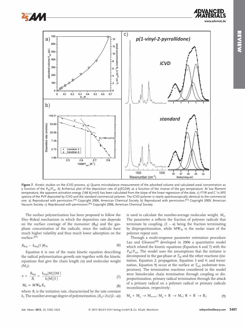
Numerous studies in literature have demonstrated that sub-strate temperature, [ 61,63 ] monomer fl ow rate, [ 64 ] and fi lament temperature [ 61 ] all impact deposition kinetics. However, the ratio between the monomer partial pressure ( P M ) and the satu-ration pressure at the substrate temperature ( P sat ) is often the dominant parameter. [ 54,64 ] Quartz crystal microbalance studies reveal that P M / P sat is directly correlated with the concentration of monomer adsorbed on the surface ( Figure 7 a) through the Brunauer–Emmett–Teller adsorption isotherm: [ 60 ]
Vad = Vmlc(PM/Psat)
(1 − PM/Psat)[1 − (1 − c)(PM/Psat)] (5)
where c ≈ exp[(�Hdes − �Hvap)/(RT )] and Vmlc(PM/Psat) = [M] ∼ Vad|PM/Psat→0 . V ad is the total adsorbed volume; V ml is the monolayer-adsorbed volume. Δ H des is the enthalpy of desorption and Δ H vap the enthalpy of evaporation.
In iCVD kinetics studies the enthalpy of evaporation, Δ H vap , determined falls in the range of 20–80 kJ/mol, which is charac-teristic of physisorption of small molecules on surfaces through van der Waals interactions. The monomer adsorption is pro-moted by low substrate temperature. Additionally, the surface concentration of monomer determines the sticking probability of the initiator radicals. [ 64 ]
GmbH & Co. KGaA, Weinheim Adv. Mater. 2013, 25, 5392–5423
REV
IEW
www.advmat.de
Figure 7. Kinetic studies on the iCVD process. a) Quartz microbalance measurement of the adsorbed volume and calculated areal concentration as a function of the P M / P sat . b) Arrhenius plot of the deposition rate of p(EGDA) as a function of the inverse of the gas temperature. At low fi lament temperature, the apparent activation energy (166 kJ/mol) has been calculated from the slope of the linear regression of the data. c) FTIR and C 1s XPS spectra of the PVP deposited by iCVD and the standard commercial polymer. The iCVD polymer is nearly spectroscopically identical to the commercial one. a) Reproduced with permission. [ 54 ] Copyright 2006, American Chemical Society. b) Reproduced with permission. [ 61 ] Copyright 2009, American Vacuum Society. c) Reprdouced with permission. [ 62 ] Copyright 2006, American Chemical Society.
The surface polymerization has been proposed to follow the Eley–Rideal mechanism in which the deposition rate depends on the surface coverage of the monomer ( θ M ) and the gas-phase concentration of the radicals, since the radicals have much higher volatility and thus much lower adsorption on the surface. [ 64 ]
Rdep ∼ kdep[I ⋅]θ M (6)
Equation 6 is one of the main kinetic equation describing the radical polymerization growth rate together with the kinetic equations that give the chain length ( υ ) and molecular weight ( M n ):
L =Rdep
Ri=
kdep[M] [IM·]
ki[M] [I·] (7)
Mn = MWM Xn (8)
where R i is the initiation rate, characterized by the rate constant k i . The number-average degree of polymerization, ( X n = 2 υ /(2 – a ))
© 2013 WILEY-VCH Verlag GAdv. Mater. 2013, 25, 5392–5423
is used to calculate the number-average molecular weight, M n . The parameter a refl ects the fraction of polymer radicals that terminate by coupling, (1 – a ) being the fraction terminating by disproportionation, while MW M is the molar mass of the polymer repeat unit.
Through a multi-response parameter estimation procedure Lau and Gleason [ 60 ] developed in 2006 a quantitative model which related the kinetic equations (Equation 6 and 7 ) with the P M / P sat . The model uses the assumptions that the initiator is decomposed in the gas-phase at T fi l and the other reactions (ini-tiation, Equation 2 ; propagation, Equation 3 and 4 ; and termi-nation, Equation 9) occur at the surface at T sub (substrate tem-perature). The termination reactions considered in the model were bimolecular chain termination through coupling or dis-proportionation, primary radical termination through the attack of a primary radical on a polymer radical or primary radicals recombination, respectively:
M⋅n + M⋅
n → Mn+m ; M⋅n + R⋅ → Mn; R⋅ + R⋅ → R2 (9)
5401wileyonlinelibrary.commbH & Co. KGaA, Weinheim

5402
REV
IEW
www.advmat.de
Chain transfer processes were not considered as termina-tion reaction because under vacuum many of them are either absent or negligible (e.g., there is no transfer to solvent). The modelization of the dependence of the fi lm growth rate and the molecular weight has been largely used to predict the feasibility of some new process or the scalability in large area reactors.
Also, the fi lament temperature plays a fundamental role in the process kinetics. While it does not infl uence the P M / P sat ratio on the surface, it does infl uence the concentration of radicals created, and hence the rate at which chains are initi-ated (Equation 6 ). Figure 7 b shows the Arrhenius plot of the deposition rate as a function of the fi lament temperature. [ 61 ] Two regimes can be observed. At low T fi l , the fi lm growth rate increases rapidly with increasing fi lament temperature, char-acteristic of a reaction-kinetics-limited-process. At high T fi l , the deposition rate is less infl uenced by the changes in the temperatures, which is characteristic of a mass-transfer-lim-ited-regime. In the kinetics-limited regime, the apparent acti-vation energy calculated experimentally from the Arrhenius plot is 166 ± 5 kJmol −1 , which is in good agreement with the activation energy required to decompose the TBPO molecule (163.6 kJ mol −1 ). In the mass-transfer-regime, the fi lament tem-perature is high enough to effi ciently decompose the initiator so the deposition kinetics is instead dominated by the diffu-sion of the radicals from the gas phase to the substrate surface. Decreasing the mass transfer resistance by increasing the gas fl ow rate increases the deposition rate in this regime (Figure 7 b).
The copolymerization kinetics follows the same rules as in conventional free-radical copolymerization reactions. The copolymer composition will depend on the monomer ratio at the surface. This surface ratio differs from the ratio in the feed gases when the monomers differ in volatility (e.g., have dif-ferent saturation pressures). Additionally, the tendency of two monomers to copolymerize was quantifi ed through the reac-tivity ratio. [ 65 ] The reactivity ratios describe the propensity of the propagating species to add a homo-monomer or the other monomer. In other words, considering a growing copolymer of generic monomers A and B, terminating with a A unit, then the reactivity ratio r A can be defi ned as the ratio between k A and k B according to the following reactions:
copol−A· + AkA−→ copol−A−A·
(10)
copol−A· + BkB−→ copol−A−B·
(11)
Analogously, the reactivity ratio r B for the growing copolymer terminating with a B unit can be identifi ed. The copolymer composition is determined by the Fineman–Ross equation [ 66 ] in the form:
f
F(F − 1) = rA
f 2
F− rB
(12)
where f is the monomer fraction in the gas feed, and F the monomer fraction at the surface.
3.2 . Retention of Organic Functional Groups
Many thin fi lm applications benefi t from a rationally designed chemistry for controlling the properties and molecular
wileyonlinelibrary.com © 2013 WILEY-VCH Verlag
interactions at the surface. For instance, in the biomedical fi eld, the chemistry of the surface, as quantifi ed by density of functional groups, is essential for controlling protein bonding or the attachment and growth of cells. [ 12,67,68 ] Additionally, the dynamic response of stimuli-responsive materials, that is to say, materials that change their properties following an external stimulus, also depends strongly on the density of functional groups on the surface. [ 69–71 ]
For these reasons, it is very important to chemically design the deposition process, choosing the right monomer with the desired functional groups. Retaining these organic functional groups is not trivial task for most CVD processes. In general, it has been observed that in order to retain the functional groups of the monomer, the deposition rate drops down to only a few nm/min. This is especially true when the monomer is the spe-cies that is fragmented to create active sites for polymerization, as in plasma enhanced CVD (PECVD), where labile functional groups are easily cleaved off. [ 72 ] In contrast, the monomer remains intact during iCVD, and thus, fully retains the organic moieties desired for surface design.
The iCVD method is a platform technology for yielding functional polymers at high deposition rates (>200 nm/min). Successful examples of polymers deposited by iCVD are poly(aminostyrene) (PAS) which displays a high density of functionalizable –NH 2 groups, [ 4 ] poly( N -isopropylacrylamide) (PNIPAAm) whose temperature-sensitive hydrophobicity is due to the presence of amide and isopropyl groups, [ 73 ] poly(glycidyl methacrylate) (PGMA) with reactive epoxy groups [ 53,74 ] or poly(hydroxyethyl methacrylate) (PHEMA) hydrogels, with hydrophilic hydroxyl moieties. [ 67,75,76 ] PGMA has been depos-ited also at extraordinary high deposition rates (600 nm/min) by iCVD from supersaturated monomer vapor ( P M / P sat > 1). [ 77 ] The possibility of obtaining polymer thin fi lms spectroscopi-cally identical to their bulk counterpart, makes iCVD a com-petitor with conventional wet processes (e.g., spin coating, dip casting, etc.) for thin-fi lm applications. The iCVD approach couples the versatility of organic chemistry for the synthesis of polymers with the advantages of dry processing, which is highly benefi cial for thin fi lm technologies and device fabrication.
High functional group retention by iCVD has been demon-strated with tens of monomers, including iCVD p(1-vinyl-2-pyrrollidone) (PVP). [ 78 ] The retention of the pyrrolidone functionality is important to achieve the hydrophilicity, bio-compatibility, and antifouling properties, characteristic of this polymer. Figure 7 c compares iCVD PVP to a convention-ally polymerized PVP standard (PVP360), dissolved in water and cast onto a Si substrate. The Fourier transform infrared (FTIR) spectroscopy, carbon 1s X-ray photoelectron spectros-copy (XPS), and 1 H NMR spectroscopy (not shown), all confi rm the similar chemical structure of the fi lms produced by both methods. Vinyl bonds are not detected in the FTIR spectra, con-fi rming that the iCVD polymerization indeed occurs through the saturation of all the vinyl bonds of the monomer.
The functional group retention has also been very benefi -cial to create nanoadhesive trenches. [ 4 ] Prototype microfl uidic structures were fabricated by reacting one side of the device coated with PAS, containing –NH 2 groups and the other side with PGMA, with epoxy groups. The high amine density of the iCVD fi lms enabled the formation of a robust nanoadhesive,
GmbH & Co. KGaA, Weinheim Adv. Mater. 2013, 25, 5392–5423

REV
IEW
www.advmat.de
which was orders of magnitude more robust than the coun-terpart obtained by depositing the polymers by PECVD with a lower density of functional groups at the surface.
High densities of functional groups are also important for creating a platform for further post-deposition reactions. Zwit-terionic coatings were obtained by reacting the fully retained tertiary amine groups of the polymer deposited by iCVD with 1,3-propane sultone. [ 79 ] A high density of zwitterionic moieties was demonstrated by both depth profi ling and angle-resolved XPS measurements in the top ca. 3 nm of the fi lm. Such a high density of zwitterionic groups is diffi cult to obtain with other techniques with comparable processing time. The zwitterionic functionalized surfaces exhibited excellent anti-fouling proper-ties against protein, carbohydrate, and bacterial adhesion.
The fragmentation of the initiator instead of the monomer molecule is the key for functional group retention. The same principle has been used in the iPECVD process. [ 57 ] During iPECVD, the chamber was fed also with TBPO, contrarily to conventional PECVD processes where any initiator is used. The presence of the initiator allowed a suffi cient density of reactive radicals to be obtained at very low plasma power density. Under these conditions the monomer fragmentation was minimal and therefore the monomer structure retention was enhanced com-pared to other PECVD processes, without compromising the deposition rate.
3.3 . Surface Design Through iCVD
3.3.1 . Robust Crosslinked Networks
Highly crosslinked and robust polymer networks are desirable for applications where durable, smooth, adhesive, and fl exible coatings are required, like biological implantations or thin fi lm electronics. [ 80 ] Inorganic fi lms generally show high durability and robustness but they are fragile and do not have the same versatility of the polymers. Very often the inorganic coatings cannot be deposited on soft substrates because the stress mis-match create wrinkles and cracks and the methods to deposit inorganic thin fi lms are generally not compatible with soft sub-strates. Frequently, this type of polymer network is sandwiched between very thin inorganic fi lms, in multilayer structures, to enhance the overall mechanical properties. [ 81–83 ] For these rea-sons, the deposition of a polymer network which shows proper-ties comparable to inorganic material, keeping tunability and fl exibility is of high technological interest.
The rigidity of a crosslinked network is related to the con-nectivity number, [ 84,85 ] (i.e., the average number of possible net-work forming bonds per atom):
<r>=
∑r
r nr∑r
nr
(13)
With n r being the number of atoms having r network
forming bonds. When the connectivity number is >2.4, the per-colation of rigidity occurs. This is the case of many inorganic materials. With iCVD it is possible to design the polymeriza-tion in order to keep the connectivity number in the range 2.3–2.4 which is typical of hard but fl exible networks.
© 2013 WILEY-VCH Verlag GAdv. Mater. 2013, 25, 5392–5423
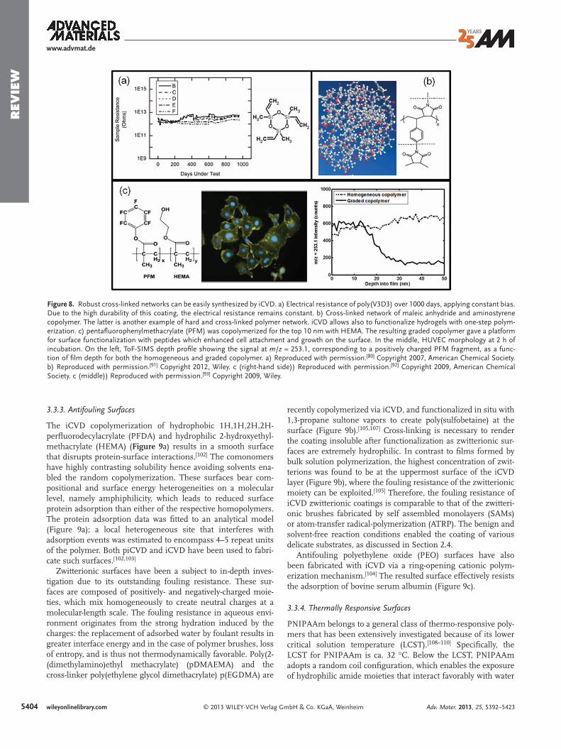
The crosslinking degree (and hence the connectivity number) can be tuned during the iCVD depositions by using monomers or comonomers (called crosslinker) with two or more vinyl bonds. [ 76,86–88 ] Polymers of trivinyltrimethylcyclotrisiloxane (V 3 D 3 ) have been investigated as biopassivating and insulating coatings for neural implants. [ 80,89,90 ] Figure 8 a shows the elec-trical resistance of poly(V 3 D 3 ) samples under simulated bioim-planted conditions and constant electrical bias. The electrical resistance remains constant over a period greater than two-and-a-half years, demonstrating the high durability of these coat-ings. At the same time, the material showed also mechanical fl exibility and good adhesion to the lead wires so that the probe could be bent without losing device reliability.
Another example of a hard and impermeable, but still fl ex-ible, organic network was obtained through the copolymeriza-tion of maleic anhydride and aminostyrene. [ 91 ] The anhydride and the amino functionalities reacted in a post-deposition annealing step iCVD and resulted in a massively cross-linked network (Figure 8 b) with elastic moduli exceeding 20 GPa. Typ-ical polymer moduli are between 0.5 and ca. 5 GPa, sensibly lower than the moduli of the cross-linked iCVD coating. The high crosslinking resulted in much lower oxygen permeability than observed for the commercial permeation barrier coatings.
3.3.2 . Functional Hydrogels: Graded Film Composition
Hydrogels are materials that can reversibly absorb water and swell, increasing their volume. This creates changes in the mechanical properties, protein adsorption capabilities and hydrophilicity of the material. This dynamic property is useful for many applications (i.e., biotechnology, [ 67,87,94 ] stimuli-responsive coatings, [ 95,96 ] sensors [ 97–99 ] etc.). Some hydrogels have similar water content to human tissue and exhibit excel-lent biocompatibility. Modifying the surface of the hydrogel keeping intact the swelling properties is a powerful tool to extend the hydrogels applicability and to target their action to specifi c drugs in drug-delivery systems or specifi c cell adhe-sion. The swelling hinders the use of solvents; therefore a dry method for the surface functionalization of hydrogel is more convenient.
Hydrogels have been deposited by iCVD (e.g., PHEMA) and they have been demonstrated to retain high swelling capability. [ 13,67,75,76,87,92,94,95,97–101 ] In addition, iCVD allowed in one-step synthesis of a functionalized hydrogel with pentafl uo-rophenyl functional groups nano-confi ned on the top surface of the material (Figure 8 c). [ 92,100 ] The deposition process was designed in order to obtain a graded composition from pure PHEMA to a copolymer of PHEMA and pentafl uorophenyl-methacrylate (PFM). Figure 8 c shows the profi le of the PFM group signal ( m / z = 253.1) as a function of fi lm depth for both the homogeneous and graded copolymer and it can be easily observed that the PFM groups are confi ned in the top 10–15 nm. The pentafl uorophenyl groups on the surface were used for further functionalization with peptides to enhance the cell growth. The homogeneous incorporation of the PFM limited the swelling ability of the hydrogel, therefore the cells did not attach on the surface. The graded copolymer instead retained the swelling ability of the pure PHEMA yielding successful cell growth.
5403wileyonlinelibrary.commbH & Co. KGaA, Weinheim
540
REV
IEW
www.advmat.de
Figure 8. Robust cross-linked networks can be easily synthesized by iCVD. a) Electrical resistance of poly(V3D3) over 1000 days, applying constant bias. Due to the high durability of this coating, the electrical resistance remains constant. b) Cross-linked network of maleic anhydride and aminostyrene copolymer. The latter is another example of hard and cross-linked polymer network. iCVD allows also to functionalize hydrogels with one-step polym-erization. c) pentafl uorophenylmethacrylate (PFM) was copolymerized for the top 10 nm with HEMA. The resulting graded copolymer gave a platform for surface functionalization with peptides which enhanced cell attachment and growth on the surface. In the middle, HUVEC morphology at 2 h of incubation. On the left, ToF-SIMS depth profi le showing the signal at m / z = 253.1, corresponding to a positively charged PFM fragment, as a func-tion of fi lm depth for both the homogeneous and graded copolymer. a) Reproduced with permission. [ 80 ] Copyright 2007, American Chemical Society. b) Reproduced with permission. [ 91 ] Copyright 2012, Wiley. c (right-hand side)) Reproduced with permission. [ 92 ] Copyright 2009, American Chemical Society. c (middle)) Reproduced with permission. [ 93 ] Copyright 2009, Wiley.
3.3.3 . Antifouling Surfaces
The iCVD copolymerization of hydrophobic 1H,1H,2H,2H-perfl uorodecylacrylate (PFDA) and hydrophilic 2-hydroxyethyl-methacrylate (HEMA) ( Figure 9 a) results in a smooth surface that disrupts protein-surface interactions. [ 102 ] The comonomers have highly contrasting solubility hence avoiding solvents ena-bled the random copolymerization. These surfaces bear com-positional and surface energy heterogeneities on a molecular level, namely amphiphilicity, which leads to reduced surface protein adsorption than either of the respective homopolymers. The protein adsorption data was fi tted to an analytical model (Figure 9 a); a local heterogeneous site that interferes with adsorption events was estimated to encompass 4–5 repeat units of the polymer. Both piCVD and iCVD have been used to fabri-cate such surfaces. [ 102,103 ]
Zwitterionic surfaces have been a subject to in-depth inves-tigation due to its outstanding fouling resistance. These sur-faces are composed of positively- and negatively-charged moie-ties, which mix homogeneously to create neutral charges at a molecular-length scale. The fouling resistance in aqueous envi-ronment originates from the strong hydration induced by the charges: the replacement of adsorbed water by foulant results in greater interface energy and in the case of polymer brushes, loss of entropy, and is thus not thermodynamically favorable. Poly(2-(dimethylamino)ethyl methacrylate) (pDMAEMA) and the cross-linker poly(ethylene glycol dimethacrylate) p(EGDMA) are
4 wileyonlinelibrary.com © 2013 WILEY-VCH Verlag G
recently copolymerized via iCVD, and functionalized in situ with 1,3-propane sultone vapors to create poly(sulfobetaine) at the surface (Figure 9 b). [ 105,107 ] Cross-linking is necessary to render the coating insoluble after functionalization as zwitterionic sur-faces are extremely hydrophilic. In contrast to fi lms formed by bulk solution polymerization, the highest concentration of zwit-terions was found to be at the uppermost surface of the iCVD layer (Figure 9 b), where the fouling resistance of the zwitterionic moiety can be exploited. [ 105 ] Therefore, the fouling resistance of iCVD zwitterionic coatings is comparable to that of the zwitteri-onic brushes fabricated by self assembled monolayers (SAMs) or atom-transfer radical-polymerization (ATRP). The benign and solvent-free reaction conditions enabled the coating of various delicate substrates, as discussed in Section 2.4.
Antifouling polyethylene oxide (PEO) surfaces have also been fabricated with iCVD via a ring-opening cationic polym-erization mechanism. [ 104 ] The resulted surface effectively resists the adsorption of bovine serum albumin (Figure 9 c).
3.3.4 . Thermally Responsive Surfaces
PNIPAAm belongs to a general class of thermo-responsive poly-mers that has been extensively investigated because of its lower critical solution temperature (LCST). [ 108–110 ] Specifi cally, the LCST for PNIPAAm is ca. 32 °C. Below the LCST, PNIPAAm adopts a random coil confi guration, which enables the exposure of hydrophilic amide moieties that interact favorably with water
mbH & Co. KGaA, Weinheim Adv. Mater. 2013, 25, 5392–5423

REV
IEW
www.advmat.de
Figure 9. iCVD surfaces for controlled interaction with protein and/or other bio-molecules and microorganisms. a) Structure and protein adsorption of antifouling iCVD p(HEMA- co -PFDA) with various compositions. Model fi tting indicates that each local heterogeneous unit that interrupts protein adsorption compasses 4–5 repeat unites. b) iCVD PEO coatings are patterned on silicon wafer and subject to adsorption tests from fl uorescently labeled bovine serum albumin (BSA); coated areas resist protein attachment effectively. c) Structure and XPS high resolution N(1s) scan of antifouling iCVD polysulfobetaine fi lm at the information depth of 3 nm. The major peak near 402 eV represents quaternary ammonium, indicating high surface concentration of zwitterions. d) Static water contact angle on multi-walled carbon nanotubes coated with iCVD PNIPAAm fi lms below (top) and above (bottom) the LCST. The mass and viscoelasticity display a step change near the LCST as revealed by Quartz-crystal microbalance with dissipation monitoring (QCM-D); above the LCST, absorbed water is expulsed from the polymer layer, which reduces the mass and the viscoelasticity. a) Repro-duced with permission. [ 100 ] Copyright 2009, Wiley. b) Reproduced with permission. [ 104 ] Copyright 2012, American Chemical Society. c) Reproduced with permission. [ 105 ] Copyright 2012, American Chemical Society. d) Reproduced with permission. [ 106 ] Copyright 2010, Wiley.
molecules; therefore, the polymer chains are hydrophilic. Above LCST, PNIPAAm chains collapse into a globular confi guration via discontinuous phase change, which renders the amide moi-eties inter- or intra-chain bonded thus leaving the hydrophobic isopropyl groups exposed; therefore PNIPAAm becomes hydro-phobic. Both homopolymer and cross-linked copolymers con-taining NIPAAm repeat units have been successfully deposited by iCVD. Cross-linkers are necessary to render the coatings insoluble in water, even below LCST. Novel graded fi lm archi-tectures with a NIPAAm-rich surface and cross-linked bulk fi lm were utilized to create faster temperature response than that can be obtained with homogeneous copolymer fi lms. [ 108 ] Drastic change in water contact angle was obtained by depos-iting cross-linked iCVD PNIPAAm conformally on multi-walled carbon nanotubes (Figure 9 d). [ 106 ] The static water contact angle jumps from 50° to 135° by increasing the system temperature of 15 °C as a result of the change in chain confi guration. [ 110 ] The confi guration change near LCST has been found to affect the mechanism of protein attachment as well. Below the LCST, the swollen hydrogel absorbs protein molecules; while above LCST, simple monolayer adsorption was observed. [ 109 ]
3.4 . Grafting and Interfacial Adhesion
3.4.1 . Trichlorovinyl Silane (TCVS) Grafting
Poor polymer-substrate adhesion is a common reason for coating failure in materials exposed to mechanical bending,
© 2013 WILEY-VCH Verlag GAdv. Mater. 2013, 25, 5392–5423
thermal stress or the effect of solvents. [ 111 ] Formation of cova-lent bonds between the polymer thin fi lm and the underlying substrate provides the highest adhesion possible to prevent delamination or detachment of the coating. [ 112 ] Surface grafting and interfacial chemical reaction are two approaches to form covalent bonds that can be readily implemented in iCVD. One means of realizing grafted iCVD interfaces is covalently bonding TCVS to a plasma-treated silicon wafer or polydime-thyldisiloxane (PDMS) surfaces via reaction of the chlorine moi-eties with the plasma generated hydroxyl groups. In the next step, radical initiators react with the vinyl group of the silane coupling agent to yield alkyl radicals that are the starting point for the grafted polymer chains. Grafting was used to create nan-opatterns on silicon wafers by colloidal lithography. [ 113 ] TCVS was attached in the interstices within a template of monodis-perse polystyrene nanoparticles cast on the silicon wafer. After iCVD polymerization, the nanoparticles were removed by soni-cation in THF leaving the polymer attached to the surface with a honeycomb structure (Figure 3 e). A specifi c example of this technique to patterning of CVD hydrogel fi lms will be dis-cussed in Section 3.5. This bottom-up process offers an inex-pensive and simple alternative to conventional lithography to design surface-functionalizable polymer patterns.
On elastomeric PDMS substrates, covalent adhesion pro-motion by TCVS resulted in robustly adhered iCVD fi lms of poly(ethylene glycol diacrylate) pEGDA. [ 114 ] The high modulus of this highly crosslinked vapor synthesized polymer relative to the PDMS substrates was critical for maintaining adhesion of
5405wileyonlinelibrary.commbH & Co. KGaA, Weinheim

5406
REV
IEW
www.advmat.de
the bilayer structure during buckling deformation. Systematic and deterministic fabrication of highly ordered herringbone patterns through sequential wrinkling strategy was demon-strated with the grafted iCVD pEGDA. This system presents a reversible behavior, switching back and forth from the ini-tial fl at surface to the ordered herringbone pattern by applying cyclic mechanical strains ( Figure 10 ).
3.4.2 . Maleic Anhydride (MA) Grafting
Vapors of maleic anhydride (MA) react directly with surface amine groups, converting them to vinyl functionalities. The
wileyonlinelibrary.com © 2013 WILEY-VCH Verlag G
Figure 10. a) SEM and FEM image of a non-equi-biaxially stretched PDMS sample upon sequential release. Adjusting the pre-stretch on the x - and y -axis and carrying out a sequential release enables to obtain a herringbone pattern and tune the features (wavelength, amplitude, jog angle) of the wrinkled pattern. b) SEM and FEM image of an equi-biaxially stretched PDMS sample upon simultaneous release. The experimental conditions carried out during the release/re-stretch process results in a disordered pattern. c) Optical 3D profi lometer image of a herringbone pattern. a–d) Reproduced with permission. [ 115 ] Copyright 2012, Wiley.
subsequent reaction of the surface vinyl bonds with monomer units to form grafted polymer chains then proceeds in the same manner as for the TCVS-produced surface vinyl moie-ties. The MA pretreatment is performed in the same vacuum chamber used for the subsequent iCVD polymer growth. Copolymers containing MA were deposited and grafted to amine-functionalized silicon nitride cantilever in a single step by iCVD. [ 116 ] A sensor was fabricated by this simple scheme, which will be discussed in greater details in Section 4.2. Using MA pretreatment, the amine groups present in the polyamide salt rejection layer of reverse osmosis (RO) membranes were turned into vinyl groups to facilitate covalent grafting of the iCVD zwitterionic polymer coating ( Figure 11 a right). [ 107 ] Without MA grafting, the vapor grown fi lms delaminated when the treated membranes where placed in water (Figure 11 a left). The grafted iCVD (Figure 11 a right) zwitterionic coating exhibited antifouling properties with respect to protein adsorption and microbial attachment. [ 105 ] By utilizing ultrathin (ca. 30 nm) iCVD antifouling layers, the water permeation rate and salt rejection of the underlying membranes was unimpaired.
3.4.3 . Tert-butyl Peroxide (TBPO) Grafting
iCVD utilizes heated fi lament to break down initiator TBPO and generate free radicals. When the fi lament temperature is below 250 °C, the labile peroxide bond is cleaved (14), which creates tert -butoxy radicals; when the fi lament temperature is above 250 °C, tert -butoxy radials start to undergo β -scission, generating methyl radicals (15), which have greater reactivity than the tert-butoxy radicals. [ 118 ]
(14)
(15)
Methyl radicals are found to facilitate the grafting of vinyl monomers to silicon hydride surfaces, namely passivating silicon surfaces. [ 117 ] This treatment was performed in the common iCVD chamber and subsequent polymer growth can be performed in situ following the surface treatment. Without this treatment, deposited fi lms delaminated from silicon sub-strate during sample trimming and handling (Figure 11 b left), and did not stand up to nanoscratching tests, where spalling of fi lms was observed (Figure 11 c left). The treated silicon sur-faces demonstrated the lowest surface recombination velocity for organic air-stable passivation methods reported to date, indi-cating the exceptional grafting quality and stability in air. The grafted iCVD coating (Figure 11 b,c) can serve as anti-refl ective coating in solar cell fabrication.
mbH & Co. KGaA, Weinheim Adv. Mater. 2013, 25, 5392–5423

REV
IEW
www.advmat.de
Figure 11. iCVD enables effective in situ grafting of deposited polymer on various substrates (right column), which enhanced the performance and durability compared to non-grafted coatings (left column). a) Without maleic anhydride (MA) grafting, antifouling iCVD zwitterionic coatings delami-nates from the membrane substrate when placed in water; while with the MA grafting, the iCVD coating, as indicated by white dots, cannot be easily differentiated from the membrane substrate, indicating good adhesion. b) Tert -butyl peroxide (TBPO) grafting enables the formation of silicon-carbon bond and the covalent attachment of polymer coatings directly to silicon substrates. The delamination events observed for non-grated coating are thus prevented. Scale bars represent 1 μ m. c) Non-grafted iCVD coating on silicon substrate does not stand up to nano-scratching tests, and spalling of the fi lms are observed under optical microscope, which does not exist for the TBPO-grafted coatings. Scale bars represent 7 μ m. a) Reproduced with permission. [ 105 ] Copyright 2012, American Chemical Society. b,c) Reproduced with permission. [ 117 ] Copyright 2013, Wiley.
3.4.4 . Nanoadhesive for Interfacial Bonding
The ring-opening reaction between amine and epoxy groups can take place at temperatures as low as 70 °C, and no gaseous by-products are produced. This avoids potential post-reaction defects resulted from outgassing and thus enables an effective nanoadhesive for interfacial bonding. This has been applied to both PDMS- and non-PDMS-based devices. [ 119,120 ] In these applications, iCVD PGMA was usually deposited on one of the interfaces to be bonded; the other surface was coated with iCVD PAS [ 120 ] (see also Section 3.3) or polyallylamine (PAAm) by plasma polymerization. [ 119 ] The two surfaces were then brought into contact with each other and cured under vacuum at 70–90 °C for 24 hours. The exceptional conformality and pinhole-free nature of iCVD method enables the fabrication of oxygen-free fl ow lithography devices with complex internal 3D structures. [ 120 ]
The amine-epoxy reaction has also been used to graft PEO coatings to amine-functionalized surfaces. The PEO coatings
© 2013 WILEY-VCH Verlag GmAdv. Mater. 2013, 25, 5392–5423
were grafted and deposited simultaneously from ethylene oxide via ring-opening cationic polymerization mechanism. [ 104 ]
3.5 . Patterning
The ability to pattern functional iCVD polymers is necessary to enable their incorporation in applications such as sensors, optical devices, and tools for biological research. Several patterning techniques have been demonstrated to date, including methods based on photo- and electron beam-lithography, imprinting, and colloidal lithography. Mao and Gleason demonstrated high-res-olution, positive-tone patterning of annealed iCVD poly(methyl α -chloroacrylate- co -methacrylic acid) via electron beam irra-diation ( Figure 12 a). [ 121 ] iCVD PGMA has also been used as a positive deep-UV resist and negative electron-beam lithography resist; [ 122,123 ] the ability to conformally coat nonplanar sur-faces [ 123 ] and use an all-dry, supercritical CO 2 developing pro-cess [ 122 ] makes this resist applicable for a range of applications.
5407wileyonlinelibrary.combH & Co. KGaA, Weinheim

5
REV
IEW
www.advmat.de
Figure 12. a) Positive-tone features patterned in a polyacrylic iCVD thin fi lm using electron-beam lithography. b) 4 mm-diameter glass rod pat-terned by exposing diacetylene-functionalized iCVD poly(4-vinylpyridine) (P4VP) through a fl exible mask. c) iCVD P4VP features patterned using a chemically non-selective lift-off technique. d) iCVD bifunctional surface exhibiting independent chemical and topological contrast. e) Nanodo-mains of iCVD and PECVD fi lms patterned using capillary force lithog-raphy; light and dark-colored regions contain orthogonal acetylene and amine functionalities, respectively. f) Arrays of self-assembled microstruc-tures created by coating elastomeric pillars with hydrophilic iCVD polymer and submerging in water. g) Close-up of a microstructure depicted in (f); solvent bonds form between the pillars, causing them to remain assem-bled after the system is dried. h) By patterning the pillar-coated substrate with regions of hydrophobic polymer, the regions of self-assembly can be controlled. a) Reproduced with permission. [ 121 ] Copyright 2006, American Chemical Society. b) Reproduced with permission. [ 124 ] Copyright 2012, Wiley. c) Reproduced with permission. [ 125 ] Copyright 2013, IEEE. d) Repro-duced with permission. [ 128 ] Copyright 2010, Wiley. e) Reproduced with per-mission. [ 126 ] Copyright 2008, American Chemical Society. f–h) Reproduced with permission. [ 127 ] Copyright 2011, American Chemical Society.
Photochemical patterning of 3D surfaces has recently been demonstrated with various iCVD polymers. Haller et al. [ 101 ] achieved positive-tone patterning of porous substrates with
408 wileyonlinelibrary.com © 2013 WILEY-VCH Verlag G
iCVD poly( o -nitrobenzyl methacrylate) (P o NBMA), a photosen-sitive polymer that can be developed in a biologically-compatible buffer. High-curvature surfaces were patterned using a resist comprised of conformal iCVD poly(4-vinylpyridine) (P4VP) functionalized with a photoactive diacetylene. [ 124 ] Coated sub-strates were covered with fl exible masks and exposed at 254 nm, which photopolymerized the diacetylene and rendered the exposed regions insoluble in the developing solvent (Figure 12 b). Bifunctional organic surfaces were also patterned; additionally, the iCVD-based resist was used to create metal microstructures via pattern transfer.
Other successful patterning strategies have been based on masking and imprinting techniques. Functional polymer fea-tures were obtained by depositing a conformal iCVD fi lm on resist templates defi ned using electron-beam lithography; the templates were then selectively removed using a non-solvent for the iCVD polymer (Figure 12 c). [ 125 ] This method is independent of the chemical functionality of the iCVD fi lm, allowing for easy exchange of responsive iCVD polymers for device appli-cations. Fabrication of bifunctional surfaces has been demon-strated using a self-aligned, dual-purpose lithographic mask (Figure 12d). [ 128 ] The resulting surfaces exhibited chemical and topological contrast and were used to achieve confi nement of water droplets during microcondensation. Capillary force lithog-raphy has also been used to pattern iCVD fi lms. [ 126 ] By pressing a heated PDMS mold onto a bilayer of highly crosslinked PECVD poly(allylamine) and iCVD polypoly(propargyl meth-acrylate), Im and coworkers were able to achieve segregation of orthogonal amine and acetylene functionalities with spatial resolution approaching 100 nm (Figure 12 e).
Self-assembly interactions were utilized to facilitate con-trollable adhesion of iCVD-coated surfaces. Chen et al. coated elastomeric pillars with hydrophilic iCVD polymers, which self-assembled into clusters upon submersion in water (Figure 12 f,g). [ 127 ] Solvent bonds formed by interpenetration of polymer chains overcome the elastic restoring force, rendering the clusters stable upon drying. By patterning some of the pillars with hydrophobic P o NBMA, the authors were able to direct self-assembly and control the location of pillar collapse (Figure 12 h).
Functional, patterned iCVD polymers have been incorpo-rated in a variety of applications. Kwong and Gupta integrated multiple unit operations into a single, paper-based microfl u-idic device. [ 129 ] Acidic iCVD poly(methacrylic acid) and basic poly(dimethylaminoethyl methacrylate) were deposited on chromatography paper and used as ion-exchange coatings for analyte separation. Patterned iCVD P o NBMA was used as a UV-responsive switch that changed hydrophobicity upon expo-sure, allowing passage of the analytes into the separation zone ( Figure 13 a). The device was successfully used to separate mix-tures of model anionic and cationic compounds (Figure 13 b–d). Haller et al. also patterned microfl uidic channels on paper using hydrophobic, photoresponsive P o NBMA (Figure 13 e). [ 101 ]
Patterned iCVD surfaces form excellent substrates for attach-ment of molecules and nanoparticles. Im and coworkers used surfaces patterned with orthogonal amine and acetylene nano-domains (Figure 12 e) to selectively self-sort fl uorescent dyes via a one-pot, biocompatible click/N-hydroxysuccinimide function-alization step (Figure 13 f). [ 126 ] Tenhaeff and Gleason synthe-sized a highly swellable, pH-responsive hydrogel, polymaleic
mbH & Co. KGaA, Weinheim Adv. Mater. 2013, 25, 5392–5423
REV
IEW
www.advmat.de
Figure 13. a) Schematic of a paper-based microfl uidic device consisting of a separation zone coated with acidic or basic iCVD polymer and a UV-responsive switch consisting of a patterned region of poly( o -nitrobenzyl methacrylate). b–d) Separation of toluidine blue O (cationic analyte) and ponceau S (anionic analyte) on an uncoated paper microfl uidic channel (b), a channel coated with acidic iCVD poly(methacrylic acid) (c), and a channel coated with basic iCVD poly(dimethylaminoethyl methacrylate) (d). e) Microfl uidic channels coated on paper using a hydrophobic, pho-toresponsive iCVD polymer. The channels exhibit excellent retention of aqueous dye solutions. f) Overlaid fl uorescence micrographs of iCVD and PECVD orthogonal nanodomains. The click-functionalized red dye is excited at 545 nm and the N-hydroxysuccinimide-functionalized green dye is excited at 491 nm. g,h) Fluorescent micrographs of an iCVD hydrogel covalently functionalized with CdSe/ZnS nanoparticles in the dry state (g) and swollen upon immersion in pH 8 buffer solution (h). a–d) Repro-duced with permission. [ 129 ] Copyright 2012, American Chemical Society. e) Reproduced with permission. [ 101 ] Copyright 2011, Royal Society of Chemistry. f) Reproduced with permission. [ 126 ] Copyright 2008, American Chemical Society. g,h) Reproduced with permission. [ 130 ] Copyright 2009, American Chemical Society.
anhydride- co -dimethylacrylamide- co -di(ethylene glycol) di(vinyl ether)] (PMaDD), for use in composite separation mem-branes. [ 130 ] The retention of functional moieties and extreme swelling response of the fi lms were confi rmed by covalently attaching CdSe/ZnS quantum dots to patterned PMaDD and imaging the fi lms upon exposure to a pH 8 buffer solution (Figure 13 g,h).
© 2013 WILEY-VCH Verlag GmAdv. Mater. 2013, 25, 5392–5423
iCVD fi lms can also be used to inhibit molecular attach-ment—for example, in the case of anti-fouling coatings. As discussed in Section 3.3.3, iCVD PEO fi lms were prepared via a ring-opening cationic polymerization mechanism. [ 104 ] PEO features were easily patterned using microcontact printing; in addition, grafted and patterned PEO regions illustrated excel-lent resistance to non-specifi c protein adsorption, in contrast to control surfaces (Figure 9 b).
3.6 . Conformality
In the surface modifi cations of non-planar substrates, the term conformality describes the ability to encapsulate the entire sur-face topography with a coating of uniform thickness and com-position. Conformal coating is desirable since it brings novel surface functionality to substrates without changing their orig-inal morphology. The conformal nature of iCVD is quite valu-able for producing functional organic coatings over surfaces having complex geometrical features. With rapid development over the past few years, iCVD has been used on many complex substrates. Even the inner surfaces of porous and fi brous sub-strates can be modifi ed with functional organic materials by iCVD. [ 131–134 ]
For solution phase processing, undesirable variations in coating thickness can result from de-wetting, liquid thinning, and surface tension effects. In contrast, the conformality of CVD polymers results from the arrival of reactants to the surface by non-line-of-sight vapor phase diffusion under the modest vacuum conditions (typically, 0.1 to 1.0 Torr), combined with the limited probability of the reactants “sticking” to the surface during a single collision. Step coverage, S, the ratio of fi lm thickness at the bottom of the feature to that at the top, is one measure of conformality. An analytic solution for iCVD fi lm growth in a trench feature gives:
ln(S) = − (� )(
L
w
)2
(16)
where ( L / w ) is the aspect ratio of the feature and Γ is the sticking coeffi cient [ 64 ] This profi le is experimentally observed when gas phase diffusion to supply additional monomer to the surface is rapid compared to the rate at which monomer is depleted by the fi lm formation reaction. Since the step coverage is governed mainly by the chemisorption of the radicals onto the adsorbed monomer sites, depositions at low fractional satu-ration partial pressure ratios ( P M / P sat ), leads to improved con-formality due to lower sticking coeffi cients. Sticking coeffi cients in the range of ca. 0.001–0.01 have been observed for iCVD.
The conformality of iCVD has been demonstrated on trench features etched into silicon, with aspect ratios up to 20:1 and on pores in various types of membranes, with aspect ratios up to 400:1. The primary variables that control the conformality of iCVD fi lms, monomer partial pressure and substrate tempera-ture, also control fi lm deposition rate. At the highest deposi-tion rates, >100 nm/min, the step coverage decreases and the thicker coating near the entrance to a cylindrical pore results in a bottleneck profi le (i.e., higher fi lm thickness at the pore
5409wileyonlinelibrary.combH & Co. KGaA, Weinheim
541
REV
IEW
www.advmat.de
Figure 14. a) SEM images of PCL electrospun mats before and after conformal iCVD coating of PPFEMA (scale bars = 2 μ m). b) XPS spectra for samples shown in (a). c) Top view SEM images of PVA mold before and after iCVD coating of PGMA and p(PFDA) (scale bar = 30 nm). The iCVD layer conformally coated inner surfaces of the polymer mold. d) Cross-sectional SEM images of iCVD deposited pCHMA on a trench wafer substrate. e) Cross-sectional SEM images of TiO 2 electrodes (4 μ m thick) before and after iCVD coating of PHEMA (scale bar = 100 nm), which keeps the morphology of the porous network unchanged. a,b) Reproduced with permission. [ 3 ] Copyright 2005, American Chemical Society. c) Reproduced with permission. [ 137 ] Copyright 2012, Elsevier. d) Reproduced with permission. [ 20 ] Copyright 2011, Wiley. e) Reproduced with permission. [ 138 ] Copyright 2011, Elsevier.
entrance). However, a high degree of conformality is still achieved at iCVD growth rates of up to 100 nm/min. This rate is quite fast compared to conformal methods for other mate-rials and is also quite reasonable since the electrolyte fi lm thick-ness of <100 nm are desired.
The limit up to which conformal coverage can be achieved has been determined by analogy to the reaction-diffusion problem commonly encountered for catalysts on porous sup-ports. [ 135 ] The analytic solution for the dimensionless monomer concentration, ψ , as a function of λ , the dimensionless distance down the pore, depends on the dimensional parameter known as the Thiele modulus, Φ :
R =eN8 + e2N−N8
1 + e2N (17)
The Thiele modulus can be readily calculated from the
dimensions of the pore, the diffusivity of the monomer, and the reaction rate. Depending on the deposition conditions, different profi les over 3D-substrates can be obtained. [ 136 ] This analysis will guide the development of conformal iCVD coating on nanostructured electrodes having different architectures, which give rise to pores of different aspect ratio.
Figure 14 a shows the micrograph of a poly(caprolactone) (PCL) nanofi ber mat before and after being iCVD coated with poly(perfl uoroalkyl ethyl methacrylate) (PPFEMA). [ 3 ] The con-formal coating by the iCVD process maintains the hierarchical nature of the electrospun mat morphology except for a slight increase in the diameter of fi bers. The comparison of the XPS survey scans before and after coating (Figure 14 b) demonstrates that the fi bers were actually coated. Figure 14 c displays a poly vinyl alcohol (PVA) mold coated by iCVD PGMA, as the sup-porting layer, and poly(1H,1H,2H,2H-perfl uorodecyl acrylate) p(PFDA), on top of PGMA layer. [ 137 ] SEM comparison between substrates with and without iCVD coating shows the conformal nature of iCVD process on the inner surfaces of the polymeric mold. The nano-scale inner surfaces features of the PVA mold are exactly repeated by the iCVD deposited fi lms. Additionally, the all-dry nature of the iCVD process avoids the possibility of the solvent swelling or damaging to the substrate, hence ruining the surface topography.
Figure 14 d shows a conformal poly(cyclohexyl methacrylate) (pCHMA) thin fi lms deposited by the iCVD process on a trench wafer. [ 132 ] This work exhibits the potential for utilizing conformal iCVD coating on microfl uidic channels. PDMS-based microfl uidic channels provide superior control over mixing than traditional batch reactions. [ 139 ] These microchan-nels need to be impermeable to liquids, but PDMS may swell in solutions. Conformal fl uoropolymer coatings by iCVD pro-cesses can serve as excellent liquid barriers of PDMS to pre-vent swelling and hydrophobic recovery caused by the low glass transition temperature of PDMS. [ 4,88,120,129,140–142 ] Riche et al. demonstrated that conformal fl uorocarbon fi lms deposited by iCVD prevent absorption of small molecules and swelling of PDMS in organic solvents. [ 88 ] This achievement provides a way to synthesize nanomaterials that are diffi cult to synthesize with conventional batch reactions. Lazarus et al. showed that devices coated in such way were used for more than 24 hours without degradation or delamination. [ 140 ] Jeong et al. deposited p(PDFA)
0 wileyonlinelibrary.com © 2013 WILEY-VCH Verlag GmbH & Co. KGaA, Weinheim Adv. Mater. 2013, 25, 5392–5423

REV
IEW
www.advmat.de
via iCVD on the PDMS micromold, which substantially reduced the diffusion of oxygen and the swelling caused by organic solvents. [ 141 ]
Conformal iCVD coatings also display excellent pore-fi lling properties, which is useful for dye-sensitized solar cells (DSSC). [ 138,143 ] iCVD polymers can replace the liquid electrolyte used in the cell and enhance its operability and durability. Figure 14 e shows pore-fi lling of a 4 μ m thick TiO 2 electrode coated with poly(2-hydroxyethyl methacrylate) (PHEMA). [ 143 ] In this work, Nejati et al. were able to achieve ca. 92–100% pore fi lling for elec-trodes as thick as 12 μ m. [ 143 ] Their research also indicated the solid state PHEMA electrolyte has higher effi ciency than the liquid elec-trolyte, and results an enhanced performance of the DSSC.
As a dry mechanism without liquid phase or excipient to produce a conformal polymerization, iCVD also provides the ability to encapsulate fi ne particles down to nanoscale without challenges of particle agglomeration, toxic solvents, and poor quality control in conventional coatings. [ 144 ]
3.7 . Templating
The substrate-independent and conformal nature of iCVD allows the coating of complex 3D surfaces to be used as a tem-plate to engineer novel and functional materials. The ability and ease to design these new-shaped materials opens the door to
© 2013 WILEY-VCH Verlag Gm
Figure 15. a,b) Confocal images of the microworms fi lled with the optode so(a) and fl uorescence mode (b). c) Fluorescent images of the tissue construmicrogroove shape. d) SEM image of the coaxial nanotubes showing a diama wall thickness of 60 nm. e) SEM image of the coaxial nanotubes after esolution at 80 °C. Due to the swelling of the hydrogel the diameter increaseswall thickness to 100 nm. Ionic liquid (IL) marbles on a liquid bath coatedPTFE particles (left) and a bare Petri dish (right). Left marble is fully encapsuretained inside the polymer shell structure showing its characteristic yellowin the right marble the IL leaked out as a result of a crack in the shell whenthe Petri dish due to the bridging effect (e). a,b) Reproduced with permis2011, National Academy of Sciences, USA. c) Reproduced with permission. [ 1
American Chemical Society. d) Reproduced with permission. [ 70 ] Copyright 20Society. e) Reproduced with permission. [ 147 ] Copyright 2012, American Chem
Adv. Mater. 2013, 25, 5392–5423
unexplored possibilities in materials development. Fabrication of responsive polymers with customized 3D structure or encap-sulation procedures for drug delivery are some examples of potential applications using the iCVD technology. Ozaydin-Ince et al. [ 99 ] conformally coated the inner walls of an anodic alu-minum oxide membrane (AAO) (pore size 200 nm and 60 μ m in length) with a 50 nm layer of p(HEMA- co -EGDA) hydrogel. The hollow left in the membrane was fi lled in with an optode solution; afterwards, both sides of the membrane were coated with the same hydrogel and fi nally the AAO membrane was etched away resulting in the release of microworms structures ( Figure 15 a,b). Due to their cylindrical shape, these biocompat-ible microworms are retained in the same location after sub-cutaneous injection more effectively than nanoparticles with equivalent diameter. Thus, microworms show potential applica-tion as fl uorescent sensors for in vivo detection and monitoring of analytes. Further studies utilized the same AAO membrane template to synthesize responsive coaxial nanotubes. [ 95 ] The coaxial deposition consisted of, fi rst, coating the AAO mem-branes walls with tert-butylacrylate copolymerized with dieth-ylene glycol divinyl ether (p(TBA- co -DEGDVE)), a memory shape polymer, and next the hydrogel copolymer p(HEMA- co -EGDA) (Figure 15 d). Immersing the nanotubes in a heated dye solution causes the hydrogel to swell; thus, widening the aper-ture of the nanotube, through which the dye diffuses and gets adsorbed (Figure 15 e). Lowering the temperature under the
bH & Co. KGaA, Wein
lution in brightfi eld ct with the PDMS
eter of 200 nm and xposure to the dye to 350 nm and the on a bed of loose lated and the IL is
ish color. However, removing it from
sion. [ 148 ] Copyright 49 ] Copyright 2011, 11, Royal Chemical
ical Society.
glass transition of the p(TBA- co -DEGDVE) fi xes the shape of the nanotube. Raising the temperature again leads to shrinkage of the memory shape polymer returning to its initial diameter. As a consequence, the dye absorbed inside is released due to the mechanical stress of the coaxial polymer. Also micro-textured PDMS surfaces have successfully been used as templates. Conformal coating of thermosensitive PNIPAAm polymer over PDMS microgrooves was used to fabricate tissue constructs. [ 68 ] Once the polymer was deposited on the PDMS surface, the micro-grooves were seeded with NIH-3T3 fi bro-blasts at a temperature of 24 °C. Conversely, for an optimal cell culture the temperature was increased to 37 °C, in which PNIPAAm is above the LCST and adopts its collapsed and hydrophobic form. After growth of the tissue, the PDMS mold is placed in contact with a glass slide at 24 °C. Temperature vari-ation drives PNIPAAm undergo transition from above to below its LCST. Therefore, the polymer swells resulting in the retrieving of the tissue construct shaped with the size of the microgroove (Figure 15 c). Besides solid substrates, Gupta and co-workers have shown that iCVD is able to coat liquids with low vapor pressure, for example, ionic liq-uids (ILs). [ 145 ] Surfaces patterned with IL and silicone oil resulted in the selective encap-sulation of IL, given that continuous iCVD fi lms can only be deposited on ILs but not on
5411wileyonlinelibrary.comheim

5412
REV
IEW
www.advmat.de
Figure 16. a) SEM images of crosslinked pHEMA-pEGDA nanotubes in the dehydrated (left) and swollen states (right). b) Cross-sectional SEMs of iCVD PHEMA coated silica microsphere at 1600X magnifi cation (left, scale bar = 10 μ m) and 5500× magnifi cation (right, scale bar = 2 μ m). c) AFM image of hydrophobic depressions in a hydrophilic matrix in dry state (left) and swollen state (right). d) Schematic of pSi capped with a pH responsive iCVD fi lm. The fi lm densifi es in low pH (left) inhibiting drug release, whereas the swelling at high pH (right) releases the drug. e) Strong hydrophilic (as shown in inset) hydrogel patterns of well-ordered PHEMA arrays grafted by iCVD process (scale bar = 1 μ m). f) SEM image of a wrinkled p(HEMA-EGDA) layer coated via iCVD process with a thick-ness of 300 ± 10 nm. a) Reproduced with permission. [ 87 ] Copyright 2010, The Royal Society of Chemistry. b) Reproduced with permission. [ 97 ] Copy-right 2008, American Chemical Society. c) Reproduced with permission.[97] Copyright 2008, American Chemical Society. d) Reproduced with permission. [ 159 ] Copyright 2012, American Chemical Society. e) Repro-duced with permission. [ 113 ] Copyright 2009, American Chemical Society. f) Reproduced with permission. [ 115 ] Copyright 2012, Wiley.
silicone oil. [ 146 ] In addition, marbles of IL were fully encapsu-lated within a polymer shell of p(PFDA- co -EGDA). [ 147 ] Rolling the marbles over a bed of loose polytetrafl uoroethylene (PTFE) particles creates a textured surface around the IL that facilitates the conformal coating of the polymer to form a shell. The struc-ture of the encapsulated marbles is stable after removal from the substrate and shows no evidence of leaking.
4 . Responsive iCVD Surfaces and Devices
4.1 . Responsive Surfaces
The ability to dynamically alter surface properties is useful in a wide range of applications including biosensors, cell culture, microfl uidics, and tissue engineering. The response of the sur-face can depend on externally applied stimuli, such light, [ 150–152 ] temperature, [ 87 ] or pH. [ 153–155 ] The high degree of organic func-tional group retention by the iCVD synthesis method is essen-tial for achieving the responsiveness.
With biocompatibility and well-known hydrogel properties, PHEMA is widely used in biological and biomedical applica-tions. [ 156–158 ] Ozaydin-Ince et al. [ 87 ] fabricated pHEMA-based hydrogel nanotubes within the pores of AAO templates. Crosslinking prevented dissolution of the iCVD layer when exposed to aqueous solution. As shown in Figure 16 a, the well-ordered nanotube arrays exhibit responsive behavior. [ 87 ] The swelling ratio achieved depends on the crosslinking ratio. Because swelling of the iCVD fabricated hydrogel nanoforest is not limited by the substrate, a larger degree of swelling is achieved than for a thin fi lm hydrogels. Moreover, switchable hydrophilicity nanotubes can provide a novel approach to con-trol protein adsorption and drug release. Figure 16 b shows a conformal PHEMA layer coated by iCVD on a silica micro-sphere. [ 97 ] The PHEMA layer brings an enhancement of the surface resistance to adhesion of nonspecifi c protein. This work suggests iCVD provides an ideal route to coat particle sensors, which can be as small as 5 μ m. [ 97 ]
iCVD has also been used to micropattern bifunctional sur-faces (see also Section 3.5). Baxamusa et al. used iCVD process combined with physical masks (TEM grid) to synthesize all-polymer patterned surfaces with identical control over chemical and topographic features. Figure 16 c shows an AFM image of hydrophobic depressions in a hydrophilic matrix, where the height of the hydrophilic walls changes due to swelling. Dynamic microcondensation experiments indicate water prefer-entially condensing on the hydrophilic region of the bifunctional surface.
iCVD represents a room temperature encapsulation method, which is important for thermally sensitive materials. Lau et al. [ 154 ] use a methacrylic acid (MAA) and ethyl acrylate (EA) copolymer as encapsulating layer to provide enteric release properties with pH-responsive swelling behavior of the copolymer. Karaman et al. [ 160 ] deposited poly(2-(diisopropylamino) ethyl meth-acrylate) (PDPAEMA) via iCVD on a rough substrate, which generate a surface that can switch between superhydrophobic and superhydrophilic state. Especially, the surface amino groups can be protonated at high pH and then react with anionic bio-logical materials. McInnes et al. [ 159 ] developed a controlled drug delivery system with iCVD deposited pH-responsive polymers.
wileyonlinelibrary.com © 2013 WILEY-VCH Verlag GmbH & Co. KGaA, Weinheim Adv. Mater. 2013, 25, 5392–5423

REV
IEW
www.advmat.de
Figure 17. a) TEM of a titania-iCVD PHEMA Bragg mirror deposited on silicon and b) its green color in the dry state ( t = 0 s), changing to red after exposure to water vapor ( t = 0.3 s), and recovering to green after purging with N 2 ( t = 0.6 s). c) Titania-iCVD PHEMA Bragg mirror deposited on red paper. d) iCVD polymer-coated microcantilever switch before (top) and after (bottom) exposure to hexylamine analyte. e) Micro-scale silicon trench sensor before (top) and after (bottom) exposure to nitrobenzene. f) Microscale nitroaromatic sensor consisting of a line of responsive iCVD P4VP overlaid with a nano-scale metal line. a–c) Repro-duced with permission. [ 165 ] Copyright 2008, American Chemical Society. d) Reproduced with permission. [ 116 ] Copyright 2009, IEEE. e) Reproduced with permission. [ 167 ] Copyright 2010, Wiley. f) Reproduced with permis-sion. [ 125 ] Copyright 2013, IEEE.
The drug was loaded in porous Si (pSi), then capped with a pH-responsive copolymer fi lm via iCVD (Figure 16 d). Their results show the drug release rate in the system increased more than 4 times from pH 1.8 to pH 7.4. Remarkably, this approach does not affect or degrade the drug, and the iCVD process was inde-pendent of both pore and surface chemistry.
iCVD can also be used along with colloidal lithography to provide simple and inexpensive technique for creating various polymeric nanostructures with functional patterns up to 500 nm high without harmful solvents (see also Section 3.5). [ 113 ] Figure 16 e shows grafted hydrophilic hydrogel patterns of well-ordered PHEMA arrays deposited by iCVD. [ 113 ]
iCVD can also be used to create wrinkling surface pat-terns, which are important in a wide range of applications (see Section 3.4.1). In Figure 16 f, wrinkling surface patterns of poly(2-hydroxyethyl methacrylate-ethylene glycol diacrylate) [p(HEMA-EGDA)] were deposited via iCVD process on PDMS substrates. [ 114 ] The wrinkling patterns provide an approach to create ordered herringbone patterns, and more important, the ability to probe the surface topologies via simplifi ed theoretical model, and a way to measure the elastic modulus of the fi lm.
4.2 . Responsive Devices
Exact control over the composition, thickness, and conformality of iCVD polymer thin fi lms can be achieved by controlling the deposition conditions. This, as well as the ease of integrating iCVD with standard semiconductor manufacturing practices, makes it an ideal technique for fabricating responsive polymer device components. iCVD fi lms have been incorporated into a variety of such applications, including biosensors, enteric coat-ings, and sensing platforms for vapor-phase analytes. Ozaydin-Ince and coworkers used an iCVD templating technique to create “microworm” optode sensors for in vivo measurement of sodium concentration (Figure 15 a–c). [ 99 ] iCVD PHEMA coatings have also been used to increase device response in impedance biosensors. [ 98 ] The hydrogel coatings protect the electrodes, enhance their surface resistance, and improve the quality of the electrode-electrolyte interface. Analyte diffusion is unaffected due to the increased pore size resulting from swelling of the fi lm in aqueous solution.
pH-responsive iCVD fi lms have been incorporated into a variety of controlled release applications. Methacrylic acid (MAA)-containing iCVD copolymers have been used as enteric coatings for pharmaceuticals. [ 153 ] The benign reaction condi-tions inherent to the iCVD process make it an ideal method for coating thermally-sensitive drugs. Encapsulation of fi ne drug particles, including microcrystals, is facilitated by the use of a rotary iCVD reactor. [ 161 , 162 ] Additionally, iCVD MAA fi lms have been used to cap the pores of biodegradable, nanoporous Si matrices loaded with a model drug compound. [ 163 ] Release of the drug from the coated matrices is four times faster at pH 7.4 than at pH 1.8, in contrast to uncoated matrices, which show similar rates at both pH values. Synthesis of the iCVD coating is facilitated by the fact that the process is independent of both the surface chemistry and pore size of the Si. iCVD has also been used to achieve controlled release of a water-soluble crop protection compound (CPC). [ 164 ] Microcapsules of the
© 2013 WILEY-VCH Verlag GmAdv. Mater. 2013, 25, 5392–5423
CPC were encapsulated with iCVD poly(glycidyl methacrylate) and poly(cyclohexyl methacrylate), and the impact of monomer hydrophilicity, coating thickness, and cross-linking density on CPC release profi les was evaluated.
Responsive iCVD thin fi lms have proven useful for a diverse range of sensing applications. Karaman et al. fabricated Bragg mirrors by using a single reaction chamber to deposit alternating layers of iCVD PHEMA and hot wire CVD (HWCVD) titania with high refractive index contrast ( Figure 17 a). [ 165 ] Exposure to
5413wileyonlinelibrary.combH & Co. KGaA, Weinheim
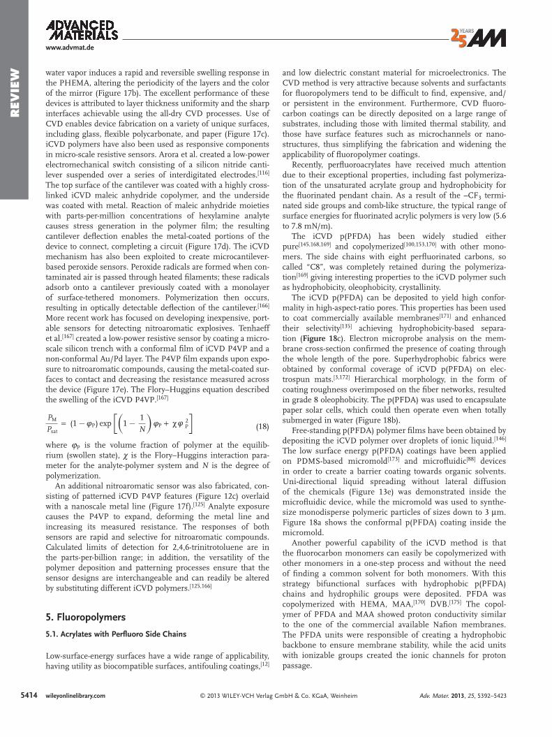
5414
REV
IEW
www.advmat.de
water vapor induces a rapid and reversible swelling response in the PHEMA, altering the periodicity of the layers and the color of the mirror (Figure 17 b). The excellent performance of these devices is attributed to layer thickness uniformity and the sharp interfaces achievable using the all-dry CVD processes. Use of CVD enables device fabrication on a variety of unique surfaces, including glass, fl exible polycarbonate, and paper (Figure 17 c). iCVD polymers have also been used as responsive components in micro-scale resistive sensors. Arora et al. created a low-power electromechanical switch consisting of a silicon nitride canti-lever suspended over a series of interdigitated electrodes. [ 116 ] The top surface of the cantilever was coated with a highly cross-linked iCVD maleic anhydride copolymer, and the underside was coated with metal. Reaction of maleic anhydride moieties with parts-per-million concentrations of hexylamine analyte causes stress generation in the polymer fi lm; the resulting cantilever defl ection enables the metal-coated portions of the device to connect, completing a circuit (Figure 17 d). The iCVD mechanism has also been exploited to create microcantilever-based peroxide sensors. Peroxide radicals are formed when con-taminated air is passed through heated fi laments; these radicals adsorb onto a cantilever previously coated with a monolayer of surface-tethered monomers. Polymerization then occurs, resulting in optically detectable defl ection of the cantilever. [ 166 ] More recent work has focused on developing inexpensive, port-able sensors for detecting nitroaromatic explosives. Tenhaeff et al. [ 167 ] created a low-power resistive sensor by coating a micro-scale silicon trench with a conformal fi lm of iCVD P4VP and a non-conformal Au/Pd layer. The P4VP fi lm expands upon expo-sure to nitroaromatic compounds, causing the metal-coated sur-faces to contact and decreasing the resistance measured across the device (Figure 17 e). The Flory–Huggins equation described the swelling of the iCVD P4VP. [ 167 ]
PM
Psat= (1 −nP) exp
[(1 − 1
N
)nP + P 2
P
]n
(18)
where ϕ P is the volume fraction of polymer at the equilib-rium (swollen state), χ is the Flory–Huggins interaction para-meter for the analyte-polymer system and N is the degree of polymerization.
An additional nitroaromatic sensor was also fabricated, con-sisting of patterned iCVD P4VP features (Figure 12 c) overlaid with a nanoscale metal line (Figure 17 f). [ 125 ] Analyte exposure causes the P4VP to expand, deforming the metal line and increasing its measured resistance. The responses of both sensors are rapid and selective for nitroaromatic compounds. Calculated limits of detection for 2,4,6-trinitrotoluene are in the parts-per-billion range; in addition, the versatility of the polymer deposition and patterning processes ensure that the sensor designs are interchangeable and can readily be altered by substituting different iCVD polymers. [ 125,166 ]
5 . Fluoropolymers
5.1 . Acrylates with Perfl uoro Side Chains
Low-surface-energy surfaces have a wide range of applicability, having utility as biocompatible surfaces, antifouling coatings, [ 12 ]
wileyonlinelibrary.com © 2013 WILEY-VCH Verlag G
and low dielectric constant material for microelectronics. The CVD method is very attractive because solvents and surfactants for fl uoropolymers tend to be diffi cult to fi nd, expensive, and/or persistent in the environment. Furthermore, CVD fl uoro-carbon coatings can be directly deposited on a large range of substrates, including those with limited thermal stability, and those have surface features such as microchannels or nano-structures, thus simplifying the fabrication and widening the applicability of fl uoropolymer coatings.
Recently, perfl uoroacrylates have received much attention due to their exceptional properties, including fast polymeriza-tion of the unsaturated acrylate group and hydrophobicity for the fl uorinated pendant chain. As a result of the –CF 3 termi-nated side groups and comb-like structure, the typical range of surface energies for fl uorinated acrylic polymers is very low (5.6 to 7.8 mN/m).
The iCVD p(PFDA) has been widely studied either pure [ 145,168,169 ] and copolymerized [ 100,153,170 ] with other mono-mers. The side chains with eight perfl uorinated carbons, so called “C8”, was completely retained during the polymeriza-tion [ 169 ] giving interesting properties to the iCVD polymer such as hydrophobicity, oleophobicity, crystallinity.
The iCVD p(PFDA) can be deposited to yield high confor-mality in high-aspect-ratio pores. This properties has been used to coat commercially available membranes [ 171 ] and enhanced their selectivity [ 135 ] achieving hydrophobicity-based separa-tion (Figure 18 c). Electron microprobe analysis on the mem-brane cross-section confi rmed the presence of coating through the whole length of the pore. Superhydrophobic fabrics were obtained by conformal coverage of iCVD p(PFDA) on elec-trospun mats. [ 3,172 ] Hierarchical morphology, in the form of coating roughness overimposed on the fi ber networks, resulted in grade 8 oleophobicity. The p(PFDA) was used to encapsulate paper solar cells, which could then operate even when totally submerged in water (Figure 18 b).
Free-standing p(PFDA) polymer fi lms have been obtained by depositing the iCVD polymer over droplets of ionic liquid. [ 146 ] The low surface energy p(PFDA) coatings have been applied on PDMS-based micromold [ 173 ] and microfl uidic [ 88 ] devices in order to create a barrier coating towards organic solvents. Uni-directional liquid spreading without lateral diffusion of the chemicals (Figure 13 e) was demonstrated inside the microfl uidic device, while the micromold was used to synthe-size monodisperse polymeric particles of sizes down to 3 μ m. Figure 18 a shows the conformal p(PFDA) coating inside the micromold.
Another powerful capability of the iCVD method is that the fl uorocarbon monomers can easily be copolymerized with other monomers in a one-step process and without the need of fi nding a common solvent for both monomers. With this strategy bifunctional surfaces with hydrophobic p(PFDA) chains and hydrophilic groups were deposited. PFDA was copolymerized with HEMA, MAA, [ 170 ] DVB. [ 175 ] The copol-ymer of PFDA and MAA showed proton conductivity similar to the one of the commercial available Nafi on membranes. The PFDA units were responsible of creating a hydrophobic backbone to ensure membrane stability, while the acid units with ionizable groups created the ionic channels for proton passage.
mbH & Co. KGaA, Weinheim Adv. Mater. 2013, 25, 5392–5423
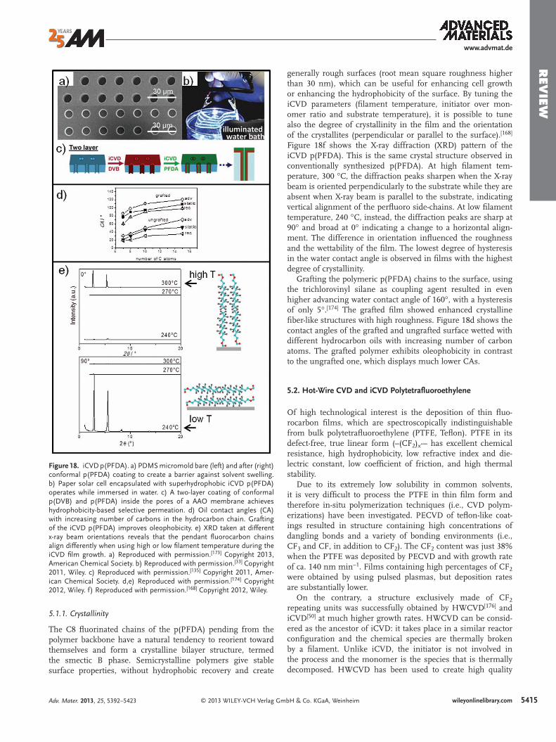
REV
IEW
www.advmat.de
Figure 18. iCVD p(PFDA). a) PDMS micromold bare (left) and after (right) conformal p(PFDA) coating to create a barrier against solvent swelling. b) Paper solar cell encapsulated with superhydrophobic iCVD p(PFDA) operates while immersed in water. c) A two-layer coating of conformal p(DVB) and p(PFDA) inside the pores of a AAO membrane achieves hydrophobicity-based selective permeation. d) Oil contact angles (CA) with increasing number of carbons in the hydrocarbon chain. Grafting of the iCVD p(PFDA) improves oleophobicity. e) XRD taken at different x-ray beam orientations reveals that the pendant fl uorocarbon chains align differently when using high or low fi lament temperature during the iCVD fi lm growth. a) Reproduced with permission. [ 173 ] Copyright 2013, American Chemical Society. b) Reproduced with permission. [ 33 ] Copyright 2011, Wiley. c) Reproduced with permission. [ 135 ] Copyright 2011, Amer-ican Chemical Society. d,e) Reproduced with permission. [ 174 ] Copyright 2012, Wiley. f) Reproduced with permission. [ 168 ] Copyright 2012, Wiley.
5.1.1 . Crystallinity
The C8 fl uorinated chains of the p(PFDA) pending from the polymer backbone have a natural tendency to reorient toward themselves and form a crystalline bilayer structure, termed the smectic B phase. Semicrystalline polymers give stable surface properties, without hydrophobic recovery and create
© 2013 WILEY-VCH Verlag GmAdv. Mater. 2013, 25, 5392–5423
generally rough surfaces (root mean square roughness higher than 30 nm), which can be useful for enhancing cell growth or enhancing the hydrophobicity of the surface. By tuning the iCVD parameters (fi lament temperature, initiator over mon-omer ratio and substrate temperature), it is possible to tune also the degree of crystallinity in the fi lm and the orientation of the crystallites (perpendicular or parallel to the surface). [ 168 ] Figure 18 f shows the X-ray diffraction (XRD) pattern of the iCVD p(PFDA). This is the same crystal structure observed in conventionally synthesized p(PFDA). At high fi lament tem-perature, 300 °C, the diffraction peaks sharpen when the X-ray beam is oriented perpendicularly to the substrate while they are absent when X-ray beam is parallel to the substrate, indicating vertical alignment of the perfl uoro side-chains. At low fi lament temperature, 240 °C, instead, the diffraction peaks are sharp at 90° and broad at 0° indicating a change to a horizontal align-ment. The difference in orientation infl uenced the roughness and the wettability of the fi lm. The lowest degree of hysteresis in the water contact angle is observed in fi lms with the highest degree of crystallinity.
Grafting the polymeric p(PFDA) chains to the surface, using the trichlorovinyl silane as coupling agent resulted in even higher advancing water contact angle of 160°, with a hysteresis of only 5°. [ 174 ] The grafted fi lm showed enhanced crystalline fi ber-like structures with high roughness. Figure 18 d shows the contact angles of the grafted and ungrafted surface wetted with different hydrocarbon oils with increasing number of carbon atoms. The grafted polymer exhibits oleophobicity in contrast to the ungrafted one, which displays much lower CAs.
5.2 . Hot-Wire CVD and iCVD Polytetrafl uoroethylene
Of high technological interest is the deposition of thin fl uo-rocarbon fi lms, which are spectroscopically indistinguishable from bulk polytetrafl uoroethylene (PTFE, Tefl on). PTFE in its defect-free, true linear form (–(CF 2 ) x -– has excellent chemical resistance, high hydrophobicity, low refractive index and die-lectric constant, low coeffi cient of friction, and high thermal stability.
Due to its extremely low solubility in common solvents, it is very diffi cult to process the PTFE in thin fi lm form and therefore in-situ polymerization techniques (i.e., CVD polym-erizations) have been investigated. PECVD of tefl on-like coat-ings resulted in structure containing high concentrations of dangling bonds and a variety of bonding environments (i.e., CF 3 and CF, in addition to CF 2 ). The CF 2 content was just 38% when the PTFE was deposited by PECVD and with growth rate of ca. 140 nm min −1 . Films containing high percentages of CF 2 were obtained by using pulsed plasmas, but deposition rates are substantially lower.
On the contrary, a structure exclusively made of CF 2 repeating units was successfully obtained by HWCVD [ 176 ] and iCVD [ 50 ] at much higher growth rates. HWCVD can be consid-ered as the ancestor of iCVD: it takes place in a similar reactor confi guration and the chemical species are thermally broken by a fi lament. Unlike iCVD, the initiator is not involved in the process and the monomer is the species that is thermally decomposed. HWCVD has been used to create high quality
5415wileyonlinelibrary.combH & Co. KGaA, Weinheim
5416
REV
IEW
www.advmat.de
Figure 19. iCVD and HWCVD PFTE. a) Nanotube coated with con-formal 40-nm-thick PFTE fi lm. b) Perfectly rounded-shape of a water droplet deposited on PFTE-coated nanotube forest. c) PTFE deposited by HWCVD on paper substrate. The mild deposition conditions did not damage the paper substrate. d,f) PTFE deposited on a lead wire (d) and on a MEMS test structure (f) to show the conformality that can be achieved by HWCVD. e) Solid-state magic angle spinning 19 F NMR spec-troscopy, which shows that the HWCVD PTFE is made essentially of -CF 2 repeating units as the bulk Tefl on. g–i) Crystalline lamellar PTFE chains were obtained on single walled carbon nanotubes (SWCNT). Such mor-phology was called “shish kebab” nanohybrid: (g) SEM image of SWCNT buckypaper with a thin coating of PTFE, (h) Histogram of the diameters of the shish kebab structure. i) Schematic of the disks arrangement on the SWCNT bundle. a,b) Reproduced with permission. [ 182 ] Copyright 2003, American Chemical Society. c) Reproduced with permission. [ 131 ] Copy-right 2006, Elsevier. d) Reproduced with permission. [ 183 ] Copyright 1996, American Institute of Physics. e) Reproduced with permission. [ 181 ] Copy-right 2000, Elsevier. f) Reproduced with permission. [ 2 ] Copyright 2010, Wiley. g–i) Reproduced with permission. [ 51 ] Copyright 2012, Wiley.
fl uorocarbon and organosilicon fi lms and has attracted signifi -cant attention due to the scalability of the process. [ 131,177 ] The monomer, which has been used to create PTFE fi lms, is the hexafl uoropropylene oxide (HFPO). HFPO pyrolysis results in difl uorocarbene (CF 2 :) radicals. [ 178 ] CF 2 production has been observed in the gas phase by UV absorption spectroscopy. [ 179 ] PTFE chain growth proceeds by the addition of singlet CF 2 to unterminated C n F 2 n chains, following the pathway identifi ed by density functional theory. [ 180 ] Chain termination most likely occurs by reaction with the primary initiating radical or with another propagating chain.
PTFE fi lms produced by HWCVD technique can reach essential 100% CF 2 groups. Measurements of X-ray photoelec-tron spectroscopy (XPS) and Fourier transform infrared (FTIR) spectra demonstrate the predominance of the –CF 2 – bonding environment, similarly to what also observed for conventionally synthesized bulk PTFE. Same results were obtained by solid-state magic angle spinning 19 F NMR spectroscopy as shown in Figure 19 e. [ 181 ] The PTFE obtained by HWCVD showed also some crystalline organization as observed by X-ray diffraction (XRD), which was enhanced by an annealing step to the point that spherulites were visible to the naked eye. [ 5 ]
Typical surface energy for PTFE is ca. 20 mN/m, higher than the surface energy of the acrylate-based fl uorocarbon coating, due to the low density of terminal CF 3 groups. In spite of this, superhydrophobic coatings were obtained by depositing con-formal PTFE by HWCVD over vertically aligned multiwalled carbon nanotube forests (mean diameter of ca. 50 nm, mean height of ca. 2 μ m) (Figure 19 a). [ 182 ] Figure 19 b shows an essen-tially spherical water droplet suspended on the PTFE-coated forest. PTFE coated nanotube forest displayed advancing and receding contact angles with water of 170° and 160°, respec-tively. The super-hydrophobicity was explained as an effect of the higher roughness due to the deposition on nanotubes of different height.
Also in HWCVD the substrate remains at ambient tempera-ture. This enables the coating of nearly any object, including paper. Figure 19 c shows, in fact, a PTFE-coated tissue paper. [ 131 ] The paper substrate survived the HWCVD step, demonstrating the gentle nature of the process, and the water did not wet it after depositing the hydrophobic coating. In contrast, sub-strates need to withstand a temperature of 400 °C in order to survive the conventional spray and bake process for PTFE coat-ings used for relative thick coatings (ca. 25 μ m), such as those applied to non-stick cookware.
HWCVD has been used to coat substrates with complex 3D shape and morphology (Figure 19 d,f). A conformal coating 16 μ m thick PTFE, was deposited on a 25 μ m diameter stainless steel wire. [ 183 ] The coating is visible all around the circumfer-ence of the wire. [ 176 ] The uniformity of coating thickness can be also observed over all the surfaces of a MEMS test structure. [ 2 ]
PTFE has been also obtained through iCVD, using the ini-tiator perfl uorooctane sulfonyl fl uoride (PFOS). [ 50 ] Thermal decomposition of the PFOS over the heated nichrome fi lament, produced·(CF 2 ) 7 CF 3 initiating radicals. For iCVD PTFE, the fi lament not only was useful to create radical species from the initiator, but also, to decompose the precursor gas (HFPO) to form the polymerizing species. The addition of PFOS, as initi-ator, accelerated the deposition rates, <1 μ m/min. Furthermore,
wileyonlinelibrary.com © 2013 WILEY-VCH Verlag
PFOS initiating radicals contained terminal CF 3 groups which were included in the PTFE polymer chains, lowering the sur-face energy of the polymer. iCVD synthesis of CF 3 terminated PTFE chains was confi rmed by solid-state magic angle spin-ning 19 F NMR spectroscopy.
Laird et al. [ 51 ] have recently investigated the use of another initiator: the perfl uorobutane sulfonyl fl uoride (CF 3 (CF 2 ) 3 SO 2 F, PBFS). It has a shorter C4 perfl uorinated chain, which is pref-erable to avoid bioaccumulating C8 species. They have inves-tigated the nanoscale roughness and chain orientation of the ultrathin iCVD PTFE conformal coatings on single wall carbon
GmbH & Co. KGaA, Weinheim Adv. Mater. 2013, 25, 5392–5423
REV
IEW
www.advmat.de
Figure 20. Commercial, automated iCVD reactors systems: a) Research tool with 0.2 m diameter vacuum chamber, b) Batch production tool with a front opening door 1.2 width, and c) Roll-to-roll system for coating fl ex-ible media up to 0.5 m in width.
nanotubes (SWCNT). The SWCNT induced PTFE crystal-lization in situ. Figure 19 g shows the SEM image of SWCNT buckypaper with a thin coating of PTFE. The PTFE shows lamellar structures, with a disk shape, spaced on average 13 nm apart and kept strung together by a one-dimensional template, presumably SWCNT bundles. This type of structure (reported for the fi rst time by this research group) has been assembled to “nanohybrid shish kebabs” in which the shishes are the nuclea-tion templates onto which crystalline polymers crystallize with lamellar orientation. A schematic of the disks arrangement on the SWCNT bundle has been given in Figure 19 i. Detailed size analysis showed that the mean diameter of the disks was ca. 40 nm (Figure 19 h). The achieved control not only over the surface chemistry of the PTFE fi lms but also on their topology is expected to have major implications in applications as anti-fouling and wear-resistant surfaces.
6 . Scale-up and Commercialization
The industrial viability of iCVD PTFE has been demonstrated by Pryce Lewis et al. [ 177 ] Computer control of the reactant fl ow rates, the temperatures of various parts of the system, pressure, and the safety interlocks, reduces the training and knowledge required by the operator of a commercial iCVD reactor system ( Figure 20 ) and improves the reproducibility of the process. The same reactor designs provide a unifi ed platform for the growth of any iCVD functional polymer or copolymer.
A benchtop system with a 200 mm diameter vacuum chamber (Figure 20 a) is designed to facilitate academic and industrial research and development. Reactor chambers with large deposition areas improve the economics of the process, increase process throughput, and allow for the surface modifi -cation of large objects. Computational fl uid dynamic modeling and non-dimensional analysis of convective and diffusive heat and mass transport [ 74 ] allow processes developed in bench scale systems to be translated with equivalent performance into large reactors. The design of the reaction chamber and the process conditions employed (temperatures, pressures, and reactant fl ow rates) determines the deposition rate achieved and the effi -ciency of reactant utilization. The latter two factors are among the most critical for determining the overall process cost. Uti-lizing reactants commercially available in bulk quantities, as opposed to custom synthesized molecules, is highly desirable for achieving favorable process economics for CVD polymers.
Two production size iCVD reaction chambers are shown in Figure 20 b and 20 c, a batch deposition reactor with an integrated touch screen control panel and a coating width of 1.2 m, and a 0.5 m wide roll-to-roll web system for coating of fl exible media, respectively. The roll-to-roll system can achieve a higher percentage of active coating time by elimi-nating the down periods associated with pumping up and pumping down each time the door is opened and closed. Semi-continuous roll-to-roll systems are typically designed to run for approximately 0.5 day or approximately 1 day without operator intervention, requiring greater process stability and control than for batch operation. Rolling the media averages any gradients present along the direction of travel, but excel-lent uniformity of composition and thickness is required in
© 2013 WILEY-VCH Verlag GmAdv. Mater. 2013, 25, 5392–5423
the perpendicular direction across the roll. The economic ben-efi t of roll-to-roll operation, for example, is utilized for metal-lization of food packages such as on the internal surfaces of potato chip bags.
5417wileyonlinelibrary.combH & Co. KGaA, Weinheim
5418
REV
IEW
www.advmat.de
While the initial investment in bench scale CVD equipment exceeds that required for typical solution processing, at the manufacturing scale CVD can have a lower cost of ownership. For example, for the growth of low dielectric constant layers for the semiconductor industry, the purchase and operation of both automated, controlled vapor ambient, spin-coating tracks and post bake furnaces for removing residual solvent, com-bined with high consumable cost of the spin-on resins, made solution-based approaches more costly than CVD. The CVD materials also had superior properties and thus now dominate the market for low dielectric constant fi lms, despite signifi cant investment from many major chemical suppliers offering solu-tion applied low dielectric materials. Commercialization of solvent-free CVD processes can also be favored by the absence of environmental, health, and, safety issues associated with sol-vent usage and the elimination of solvent disposal costs.
It should be noted that an older CVD process for poly-para-xylylene (PPX) and its variants, has been successfully com-mercialized since the 1960’s. [ 184 ] These coatings, as known as parylenes, are desired for their conformal coverage and are widely used as protective encapsulation over the complex fea-tures of printed circuit boards and medical devices. An excel-lent review of the synthesis and applications of functionalized forms of PPX has been recently been authored by Chen and Lahann. [ 185 ]
7 . Historical Development
The fi rst HWCVD polymer deposition in 1996 [ 183 ] was actu-ally a negative result! At that time, our MIT group had been carrying out traditional plasma enhanced CVD of polymer-like thin fi lms. In the literature for this fi eld, it was widely hypoth-esized that the ions produced by the plasma were essential for the growth of organic fi lms. [ 7 ] We were using a monomer, hexafl uoropropylene oxide (HFPO), which we subsequently learned was also thermally cracked for use in molecular beam experiments to produce the neutral species, difl uorocarbene (CF 2 ). Since we were also carrying our research on HWCVD of polycrystalline diamond thin fi lms, we decided to test the long-standing hypothesis by thermally decomposing HFPO in a HWCVD reactor, to produce a high concentration of neutrals in the absence ions. The expectation was that no fi lm would form. The wire temperatures needed for pyrolysis of the HFPO were only around 450 °C rather the 2000 °C used in the diamond deposition work. Surprisingly, in fi rst HWCVD from HFPO, doctoral student Scott Limb rapidly deposited fi lm with essen-tially 100% functional group retention.
Since this initial unanticipated result, the conceptual devel-opment of iCVD and oCVD has been guided by the work of the many researchers who established the fundamental mecha-nisms of solution phase polymerization. Several generations of graduate students and postdoctoral researchers contributed to the development of these technologies for CVD polymeriza-tion and only a few highlights will be mentioned. A separate intentional initiation species was fi rst introduced by doctoral student Hilton Pryce Lewis in 2001, [ 50 ] yielding a dramatic increase in deposition rate. As CEO of GVD Corporation (gvd-corp.com), Dr. Pryce Lewis has led the scale up, automation,
wileyonlinelibrary.com © 2013 WILEY-VCH Verlag
and commercialization of HWCVD and iCVD polymers. The utilization of a separate initiator was extended by doctoral student Yu (Jessie) Mao to the fi rst successful polymerization vinyl monomers in 2004. [ 53 ] She also demonstrated the fi rst iCVD copolymerization and extended the use of reactivity ratios developed for solution synthesis to the vapor deposited fi lms. Fundamental knowledge of the iCVD process was signifi cantly advanced by doctoral student Kenneth K. S. Lau. [ 54,60 ] Thus, the iCVD method could be rapidly extended to the free radical polymerization of many new monomers. Also in 2006, the fi rst demonstration of oxidative step growth polymerization to form oCVD electrical conductive fi lms was achieved by doctoral can-didate John Lock. [ 24 ] The in situ grafting of oCVD fi lm to create robust adhesion to surfaces with aromatic groups was achieved by doctoral student Sung Gap Im. [ 19 ] In 2012, as a professor at Drexel, Dr. Lau has shown that iCVD can be extended to cati-onic polymerization. [ 104 ]
The polymeric compositions achievable and their applica-tions are anticipated to blossom as more research groups adopt this technology.
8 . Conclusions and Future Prospects
New CVD polymer methods augment the capabilities of tradi-tional methods for polymeric surface modifi cation and are an enabling technology for multiple applications. CVD polymeri-zation brings the precision of the vacuum deposition methods developed for inorganic fi lms to the realm of functional and responsive organic materials. Vapor methods enable the direct chemical synthesis and thin fi lm formation of organic polymer layers in a single step. The platform technologies of oCVD and iCVD are analogous to traditional oxidative step growth and free radical chain growth mechanisms, respectively.
The full degree organic functional group retention is highly desirable for designing surfaces, which display controlled wet-tability, antifouling behavior, or respond to external stimuli. Additionally, the chemical and biological specifi city, which can be imparted by the organic functional groups, is a characteristic that clearly differentiates CVD polymers from their inorganic CVD counter parts. This specifi city of chemical and biological interaction is only beginning to be exploited for applications from chemical sensing to tissue engineering.
A wide range of homopolymers and copolymer compositions have been demonstrated by both iCVD and oCVD methods. A unique feature of CVD is that the monomers used for the copo-lymerization do not require a common solvent.
Dielectrics, semiconductors, and electronic conductors have all been demonstrated by CVD polymerization. Contiguous fi lms can be obtained with thickness as low as 10 nm, while high growth rate conditions, in some cases >1 μ m/min, can be utilized to deposit fi lms which are tens of micrometers thick.
The easy tunablity of the fi lm and surface properties has allowed the successful integration of CVD polymers into proto-types for applications including, but not limited to, membranes, microfl uidics, sensors, controlled release, and fl exible optoelec-tronics. As passivation of neural probes, dielectric iCVD layers have measured stability over more than 9 years in 37 °C saline solution under continuous cycling between +5 V and −5 V.
GmbH & Co. KGaA, Weinheim Adv. Mater. 2013, 25, 5392–5423
REV
IEW
www.advmat.de
The diversity of applications for CVD polymers is anticipated to expand with increasing codifi cation of the processing knowl-edge and ready availability of automated reactor systems.
By eliminating the need to dissolve macromolecules, the CVD approach is particularly advantageous for the synthesis of linear polymers or crosslinked networks of limited solubility. Additionally, vapor processing avoids the potential for the sub-strate to disintegrate, dissolve, swell, shrink, fade, or wrinkle as a result of solvent exposure. Solvent-free and surfactant-free processing eliminates the environmental, safety, and health considerations associated with these components and can reduce waste disposal. Process simplifi cation can result by eliminating post-deposition steps, such as annealing for removing residual solvent from solution-applied fi lm. Undesir-able dewetting effects, which lead to pinhole and void forma-tion, are also avoided by utilizing CVD.
Unlike typical solution processing, CVD polymerization pro-duces conformal coatings, which precisely follows the geometry of the underlying substrate. The conformal nature of CVD poly-mers allows the uniform modifi cation of objects having com-plex shapes and surface features, including the interior sur-faces of porous or fi ber-based media. This conformal behavior has been achieved at high rates (ca. 100 nm/min). The high deposition rate and the specifi c chemical composition of the resulting polymers differentiate iCVD and oCVD conformal coatings from those achieved by either atomic layer deposition (ALD) or layer-by-layer (LBL) deposition.
By building the fi lms from the interface up, in situ inter-facial grafting strategies have resulted in robust interfaces. To date, these grafted interfaces have been shown to prevent delamination failures, which is essential for most applications. The adhesion allows patterning the functional layers to sub-micrometer resolution and this patterning is essential for the successful integration of CVD polymer into device structures. In addition, grafted iCVD interfaces have enabled the stable electronic passivation of silicon at room temperature. Future efforts are expected to produce hybrid organic/inorganic inter-faces with novel thermal and electronic properties.
The modest substrate temperature, often near room tempera-ture, allows the CVD polymers to be directly grown on thermal sensitive materials, such as plastics and textiles. In contrast, materials synthesized at high temperature must be fi rst grown on thermal stable substrate and then transferred onto the substrate of lower thermal stability, through a complex and costly process. Since fl exible substrates are essential for economical roll-to-roll manufacturing, the ability to grow fl exible layers of insoluble materials, including electrical conductors and semiconductors, directly on fl exible substrates, is an enabling capability for low-cost processing. Additionally, the controlled vacuum deposition environment and the high purity of commercially available small molecule reactants enable high quality fi lm, making CVD poly-mers desirable for biomedical and optoelectronic applications. Precise control and quantitative modeling of the delivery of reac-tants, vapor fl ow patterns, and reaction temperatures, couples with real-time monitoring of the deposited thickness allow for reproducible of processing and scale up of reactor size. These two latter factors have been the key to the commercial success demonstrated to date, and will remain essential to further expan-sion of the many practical benefi ts of CVD polymer technology.
© 2013 WILEY-VCH Verlag GmAdv. Mater. 2013, 25, 5392–5423
Acknowledgements This article is part of an ongoing series celebrating the 25th anniversary of Advanced Materials. The authors acknowledge fi nancial support from the MIT Institute for Soldier Nanotechnologies (ISN) under Contract DAAD-19–02D-0002 with the U.S. Army Research Offi ce, the King Fahd University of Petroleum and Minerals (KFUPM) in Dhahran, Saudi Arabia, for funding support through the Center for Clean Water and Clean Energy at MIT and KFUPM, and the Masdar Institute. The offi ce of Naval Research and Advanced Research Projects Agency-Energy are also kindly acknowledged. D.C.B. and C.D.P. gratefully acknowledge support from the National Science Foundation Graduate Research Fellowship Program. R.M.H. acknowledges support from Department of Energy Offi ce of Science Graduate Fellowship Program (DOESCGF), made possible in part by the American Recovery and Reinvestment Act of 2009, administered by ORISE-ORAU under Contract No. DE-AC05–06OR23100.
Received: April 26, 2013 Published online: September 25, 2013
[1] G. Ozaydin-Ince , A. M. Coclite , K. K. Gleason , Rep. Prog. Phys. 2012 , 75 , 1 – 40 .
[2] M. E. Alf , A. Asatekin , M. C. Barr , S. H. Baxamusa , H. Chelawat , G. Ozaydin-Ince , C. D. Petruczok , R. Sreenivasan , W. E. Tenhaeff , N. J. Trujillo , S. Vaddiraju , J. J. Xu , K. K. Gleason , Adv. Mater. 2010 , 22 , 1993 – 2027 .
[3] M. L. Ma , Y. Mao , M. Gupta , K. K. Gleason , G. C. Rutledge , Macro-molecules 2005 , 38 , 9742 – 9748 .
[4] J. J. Xu , K. K. Gleason , Chem. Mater. 2010 , 22 , 1732 – 1738 . [5] K. K. S. Lau , K. K. Gleason , J. Phys. Chem. B. 2001 , 105 , 2303 – 2307 . [6] J. Lahann , D. Klee , W. Pluester , H. Hoecker , Biomaterials 2001 , 22 ,
817 – 826 . [7] R. Dagostino , F. Cramarossa , F. Illuzzi , J. Appl. Phys. 1987 , 61 ,
2754 – 2762 . [8] K. Endo , T. Tatsumi , J Appl Phys. 1995 , 78 , 1370 – 1372 . [9] N. H. Lee , L. M. Christensen , C. W. Frank , Langmuir 2003 , 19 ,
3525 – 3530 . [10] P. Simon , S. Mang , A. Hasenhindl , W. Gronski , A. Greiner , Macro-
molecules 1998 , 31 , 8775 – 8780 . [11] S. Seidel , C. T. Riche , M. Gupta , in Encyclopedia of Polymer Science
and Technology , John Wiley & Sons, Inc. , New York 2002 . [12] R. Yang , A. Asatekin , K. K. Gleason , Soft Matter 2012 , 8 , 31 – 43 . [13] S. G. Im , K. K. Gleason , AIChE J. 2011 , 57 , 276 – 285 . [14] M. C. Barr , C. Carbonera , R. Po , V. Bulovic , K. K. Gleason , Appl.
Phys. Lett. 2012 , 100 , 183301 . [15] M. C. Barr , J. A. Rowehl , R. R. Lunt , J. Xu , A. Wang , C. M. Boyce ,
S. G. Im , V. Bulovic , K. K. Gleason , Adv. Mater. 2011 , 23 3500 – 3505 . [16] R. M. Jain , R. Howden , K. Tvrdy , S. Shimizu , A. J. Hilmer , T. P.
McNicholas , K. K. Gleason , M. S. Strano , Adv. Mater. 2012 , 24 , 4436 – 4439 .
[17] D. Bhattacharyya , K. K. Gleason , Chem. Mater. 2011 , 23 , 2600 – 2605 .
[18] D. Bhattacharyya , K. Senecal , P. Marek , A. Senecal , K. K. Gleason , Adv Funct. Mater. 2011 ,, 21 , 4328 – 4337 .
[19] S. G. Im , P. J. Yoo , P. T. Hammond , K. K. Gleason , Adv. Mater. 2007 , 19 , 2863 – 2867 .
[20] M. C. Barr , J. A. Rowehl , R. R. Lunt , J. Xu , A. Wang , C. M. Boyce , S. G. Im , V. Bulovi , K. K. Gleason , Adv. Mater. 2011 , 23 , 3500 – 3505 .
[21] S. G. Im , K. K. Gleason , Macromolecules 2007 , 40 , 6552 – 6556 . [22] H. Chelawat , S. Vaddiraju , K. Gleason , Chem. Mater. 2010 , 22 ,
2864 – 2868 . [23] S. Nejati , K. K. S. Lau , Langmuir 2011 , 27 , 15223 – 15229 . [24] J. P. Lock , S. G. Im , K. K. Gleason , Macromolecules 2006 , 39 ,
5326 – 5329 .
5419wileyonlinelibrary.combH & Co. KGaA, Weinheim

5420
REV
IEW
www.advmat.de
[25] D. Bhattacharyya , R. M. Howden , D. C. Borrelli , K. K. Gleason , J. Polym. Sci., Part B: Polym. Phys. 2012 , 50 , 1329 – 1351 .
[26] H. Park , R. M. Howden , M. C. Barr , V. Bulovic , K. Gleason , J. Kong , ACS Nano 2012 , 6 , 6370 – 6377 .
[27] R. M. Howden , E. J. Flores , V. Bulovi , K. K. Gleason . Org. Electron. 2013 , 14 , 2257 – 2268 .
[28] S. Vaddiraju , K. Seneca , K. K. Gleason , Adv. Funct. Mater. 2008 , 18 , 1929 – 1938 .
[29] R. M. Howden , E. D. McVay , K. K. Gleason , J. Mater. Chem. A 2013 , 1 , 1334 – 1340 .
[30] D. Bhattacharyya , R. Yang , K. K. Gleason , J. Mater. Chem. 2012 , 22 , 405 – 410 .
[31] S. Vaddiraju , H. Cebeci , K. K. Gleason , B. L. Wardle , ACS Appl. Mater. Interfaces 2009 , 1 , 2565 – 2572 .
[32] S. Vaddiraju , K. Seneca , K. K. Gleason , Adv. Funct. Mater. 2008 , 18 , 1929 – 1938 .
[33] M. C. Barr , J. A. Rowehl , R. R. Lunt , J. J. Xu , A. N. Wang , C. M. Boyce , S. G. Im , V. Bulovic , K. K. Gleason , Adv. Mater. 2011 , 23 , 3500 – 3505 .
[34] N. J. Trujillo , M. C. Barr , S. Gap Im , K. K. Gleason , J. Mater. Chem. 2010 , 20 , 3968 – 3972 .
[35] S. G. Im , K. K. Gleason , E. A. Olivetti , Appl. Phys. Lett. 2007 , 90 . [36] J.P. Lock , J. L. Lutkenhaus , N. S. Zacharia , S.G. Im ,
P. T. Hammond , K. K. Gleason , Synth. Met. 2007 , 157 , 894 – 898 . [37] V. Scardaci , R. Coull , J. N. Coleman , Appl. Phys. Lett. 2010 , 97 . [38] M. C. Barr , R. M. Howden , R. R. Lunt , V. Bulovic , K. K. Gleason ,
Adv. Energy Mater. 2012 , 2 , 1404 – 1409 . [39] M. C. Barr , C. Carbonera , R. Po , V. Bulovic , K. K. Gleason , Appl.
Phys. Lett. 2012 , 100 . [40] S. Günes , H. Neugebauer , N. Serdar Sariciftci , Chem. Rev. 2007 ,
107 , 1324 – 1338 . [41] A. P. Kulkarni , C. J. Tonzola , A. Babel , S. A. Jenekhe , Chem. Mater.
2004 , 16 , 4556 – 4573 . [42] J. Zaumseil , H. Sirringhaus , Chem. Rev. 2007 , 107 , 1296 – 1323 . [43] D. C. Borrelli , M. C. Barr , V. Bulovi , K. K. Gleason , Sol. Energy
Mater. Sol. Cells 2012 , 99 , 190 – 196 . [44] D. C. Borrelli , K. K. Gleason , Macromolecules 2013 , 46 , 6169 – 6176 . [45] D. Bhattacharyya , K. K. Gleason , J. Mater. Chem. 2012 , 22 ,
405 – 410 . [46] D. Bhattacharyya , K. Senecal , P. Marek , A. Senecal , K. K. Gleason ,
Adv. Funct. Mater. 2011 , 21 , 4328 – 4337 . [47] H. Bai , G. Shi , Sensors 2007 , 7 , 267 – 307 . [48] S. Vaddiraju , K. K Gleason , Nanotechnology 2010 , 21 , 125503 . [49] D. Bhattacharyya , K. K. Gleason , Chem. Mater. 2011 , 23 ,
2600 – 2605 . [50] H. G. Pryce Lewis , J. A. Caulfi eld , K. K. Gleason , Langmuir 2001 ,
17 , 7652 – 7655 . [51] E. D. Laird , R. K. Bose , W. Wang , K. K. S. Lau , C. Y. Li , Macromol.
Rapid Commun. 2013 , 34 , 251 – 256 . [52] K. Chan , K. K. Gleason , Chem. Vap. Deposition 2005 , 11 , 437 – 443 . [53] Y. Mao , K. K. Gleason , Langmuir 2004 , 20 , 2484 – 2488 . [54] K. K. S. Lau , K. K. Gleason , Macromolecules 2006 , 39 , 3688 – 3694 . [55] J. Xu , K. K. Gleason , ACS Appl. Mater. Interfaces 2011 , 3 ,
2410 – 2416 . [56] J. L. Yagüe , A. M. Coclite , C. Petruczok , K. K. Gleason , Macromol.
Chem. Phys. 2013 , 214 , 302 – 312 . [57] A. M. Coclite , K. K. Gleason , Plasma Process. Polym. 2012 , 9 ,
425 – 434 . [58] K. Chan , K. K. Gleason , Langmuir 2005 , 21 , 11773 – 11779 . [59] T. P. Martin , K. L. Sedransk , K. Chan , S. H. Baxamusa ,
K. K. Gleason , Macromolecules 2007 , 40 , 4586 – 4591 . [60] K. K. S. Lau , K. K. Gleason , Macromolecules 2006 , 39 , 3695 – 3703 . [61] G. Ozaydin-Ince , K. K. Gleason , J. Vac. Sci. Technol. A. 2009 , 27 ,
1135 – 1143 . [62] K. Chan , K. K. Gleason , Macromolecules 2006 , 39 , 3890 – 3894 .
wileyonlinelibrary.com © 2013 WILEY-VCH Verlag Gm
[63] A. M. Coclite , G. Ozaydin-Ince , R. d’Agostino , K. K. Gleason , Mac-romolecules 2009 , 42 , 8138 – 8145 .
[64] S. H. Baxamusa , K. K. Gleason , Chem. Vap. Deposition 2008 , 14 , 313 – 318 .
[65] G. Odian , Principles of Polymerization, 4th ed. , Wiley-Interscience , Hoboken, NJ, USA 2004 .
[66] M. Fineman , S. D. Ross , J. Polym. Sci. 1950 , 5 , 259 – 262 . [67] R. K. Bose , K. K. S. Lau , Thin Solid Films 2011 , 519 , 4415 – 4417 . [68] H. Tekin , G. Ozaydin-Ince , T. Tsinman , K. K. Gleason , R. Langer ,
A. Khademhosseini , M. C. Demirel , Langmuir 2011 , 27 , 5671 – 5679 . [69] G. Ozaydin-Ince , G. Demirel , K. K. Gleason , M. C. Demirel , Abstr.
Pap. Am. Chem. Soc. 2010 , 240 . [70] G. Ozaydin-Ince , K. K. Gleason , M. C. Demirel , Soft Matter 2011 ,
7 , 638 – 643 . [71] M. E. Alf , T. A. Hatton , K. K. Gleason , Thin Solid Films 2011 , 519 ,
4412 – 4414 . [72] R. Forch , A. N. Chifen , A. Bousquet , H. L. Khor , M. Jungblut ,
L. Q. Chu , Z. Zhang , I. Osey-Mensah , E. K. Sinner , W. Knoll , Chem. Vap. Deposition 2007 , 13 , 280 – 294 .
[73] M. E. Alf , T. A. Hatton , K. K. Gleason , Polymer 2011 , 52 , 4429e4434 . [74] M. Gupta , K. K. Gleason , Thin Solid Films 2006 , 515 , 1579 – 1584 . [75] R. K. Bose , K. K. S. Lau , Biomacromolecules 2010 , 11 , 2116 – 2122 . [76] K. Chan , K. K. Gleason , Langmuir 2005 , 21 , 8930 – 8939 . [77] R. Tao , M. Anthamatten , Langmuir 2012 , 28 , 16580 – 16587 . [78] K. Chan , L. E. Kostun , W. E. Tenhaeff , K. K. Gleason , Polymer 2006 ,
47 , 6941 – 6947 . [79] R. Yang , J. Xu , G. Ozaydin-Ince , S. Y. Wong , K. K. Gleason , Chem.
Mater. 2011 , 23 , 1263 – 1272 . [80] W. S. O’Shaughnessy , S. K. Murthy , D. J. Edell , K. K. Gleason , Bio-
macromolecules 2007 , 8 , 2564 – 2570 . [81] A. M. Coclite , G. Ozaydin-Ince , F. Palumbo , A. Milella ,
K. K. Gleason , Plasma Process. Polym. 2010 , 7 , 561 – 570 . [82] D. A. Spee , M. R. Schipper , C. H. M. van der Werf , J. K. Rath ,
R. E. I. Schropp , Thin Solid Films 2013 , 532 , 84 – 88 . [83] A. M. Coclite , F. De Luca , K. K. Gleason , J. Vac. Sci. Technol. A.
2012 , 30 . [84] M. F. Thorpe , J. Non-Cryst. Solids 1983 , 57 , 355 – 370 . [85] J. C. Phillips , J. Non-Cryst. Solids 1979 , 34 , 153 – 181 . [86] R. K. Bose , A. M. Heming , K. K. Lau , Macromol Rapid Commun.
2012 , 33 , 1375 – 1380 . [87] G. O. Ince , G. Demirel , K. K. Gleason , M. C. Demirel , Soft Matter
2010 , 6 , 1635 – 1639 . [88] C. T. Riche , B. C. Marin , N. Malmstadt , M. Gupta , Lab Chip. 2011 ,
11 , 3049 – 3052 . [89] G. Aresta , J. Palmans , M. C. M. van de Sanden , M. Creatore , J. Vac.
Sci. Technol. A. 2012 , 30 . [90] G. Aresta , J. Palmans , M. C. M. van de Sanden , M. Creatore ,
Microporous Mesoporous Mater. 2012 , 151 , 434 – 439 . [91] J. Xu , A. Asatekin , K. K. Gleason , Adv. Mater. 2012 , 24 , 3692 – 3696 . [92] L. Montero , S. H. Baxamusa , S. Borros , K. K. Gleason , Chem.
Mater. 2009 , 21 , 399 – 403 . [93] N. Mari-Buye , S. O’Shaughnessy , C. Colominas , C. E. Semino ,
K. K. Gleason , S. Borros , Adv. Funct. Mater. 2009 , 19 , 1276 – 1286 . [94] J. L. Yagüe , K. K. Gleason , Soft Matter 2012 , 8 , 2890 – 2894 . [95] G. Ozaydin-Ince , K. K. Gleason , M. C. Demirel , Soft Matter 2011 ,
7 , 638 – 643 . [96] A. M. Coclite , Surface Innovations, 2013, 1, 6. DOI: 10.1680/
si.12.00019. Available at: http://www.icevirtuallibrary.com/con-tent/article/10.1680/si.12.00019; accessed, August 2013.
[97] S. H. Baxamusa , L. Montero , J. M. Dubach , H. A. Clark , S. Borros , K. K. Gleason , Biomacromolecules 2008 , 9 , 2857 – 2862 .
[98] L. Montero , G. Gabriel , A. Guimerà , R. Villa , K. K. Gleason , Salvador Borrós , Vacuum 2012 , 86 , 2102 – 2104 .
[99] G. Ozaydin-Ince , J. M. Dubach , K. K. Gleason , H. A. Clark , Proc. Natl. Acad. Sci. USA 2011 , 108 , 2656 – 2661 .
bH & Co. KGaA, Weinheim Adv. Mater. 2013, 25, 5392–5423
REV
IEW
www.advmat.de
[100] S. H. Baxamusa , K. K. Gleason , Adv. Funct. Mater. 2009 , 19 , 3489 – 3496 .
[101] P. D. Haller , C. A. Flowers , M. Gupta , Soft Matter 2011 , 7 , 2428 – 2432 .
[102] S. H. Baxamusa , K. K. Gleason , Adv. Funct. Mater. 2009 , 19 , 3489 – 3496 .
[103] G. Ozaydin-Ince , A. Matin , Z. Khan , K. K. Gleason , Desalin. Water Treat. 2011 , 34 , 100 – 105 .
[104] R. K. Bose , S. Nejati , D. R. Stuffl et , K. K. S. Lau , Macromolecules 2012 , 45 , 6915 – 6922 .
[105] R. Yang , K. K. Gleason , Langmuir 2012 , 28 , 12266 – 12274 . [106] M. E. Alf , P. D. Godfrin , T. A. Hatton , K. K. Gleason , Macromol.
Rapid Commun. 2010 , 31 , 2166 – 2172 . [107] R. Yang , J. Xu , G. Ozaydin-Ince , S. Y. Wong , K. K. Gleason , Chem.
Mater. 2011 , 23 , 1263 – 1272 . [108] M. E. Alf , T. A. Hatton , K. K. Gleason , Polymer 2011 , 52 , 4429 –
4434 . [109] M. E. Alf , T. A. Hatton , K. K. Gleason , Langmuir 2011 , 27 ,
10691 – 10698 . [110] M. E. Alf , T. Al. Hatton , K. K. Gleason , Thin Solid Films 2011 , 519 ,
4412 – 4414 . [111] A. J. Kinloch , Adhesion and Adhesives: Science and Technology ,
Springer , New York 1987 . [112] E. M. Liston , L. Martinu , M. R. Wertheimer , J. Adhes. Sci. Technol.
1993 , 7 , 1091 – 1127 . [113] N. J. Trujillo , S. H. Baxamusa , K. K. Gleason , Chem. Mater. 2009 ,
21 , 742 – 750 . [114] J. Yin , J. L. Yague , D. Eggenspieler , K. K. Gleason , M. C. Boyce , Adv.
Mater. 2012 , 24 , 5441 – 5446 . [115] J. Yin , J. L. Yagüe , D. Eggenspieler , K. K. Gleason , M. C. Boyce , Adv.
Mater. 2012 , 24 , 5441 – 5446 . [116] W. J. Arora , W. E. Tenhaeff , K. K. Gleason , G. Barbastathis , J. Micro-
electromech. Syst. 2009 , 18 , 97 – 102 . [117] R. Yang , T. Buonassisi , K. K. Gleason , Adv. Mater. 2013 , 25 ,
2078 – 2083 . [118] G. Ozaydin-Ince , K. K. Gleason , J. Vac. Sci. Technol., A 2009 , 27 ,
1135 – 1143 . [119] S. G. Im , K. W. Bong , C.-H. Lee , P. S. Doyle , K. K. Gleason , Lab
Chip. 2009 , 9 , 411 – 416 . [120] K. W. Bong , J. Xu , J.-H. Kim , S. C. Chapin , M. S. Strano ,
K. K. Gleason , P. S. Doyle , Nat. Commun. 2012 , 3 . [121] Y. Mao , K. K. Gleason , Langmuir 2006 , 22 , 1795 – 1799 . [122] Y. Mao , N. M. Felix , P. T. Nguyen , C. K. Ober , K. K. Gleason , J. Vac.
Sci. Technol. B 2004 , 22 , 2473 – 2478 . [123] S. Yoshida , T. Kobayashi , M. Kumano , M. Esashi , J. Micro/Nano-
lithogr., MEMS, MOEMS 2012 , 11 , 023001 – 023001 . [124] C. D. Petruczok , K. K. Gleason , Adv. Mater. 2012 , 24 , 6445 – 6450 . [125] C. D. Petruczok , H. J. Choi , S. Y. Yang , A. Asatekin , G. Barbastathis ,
K. K. Gleason , J. Microelectromech. Syst. 2013 , 22 , 54 – 61 . [126] S. G. Im , K. W. Bong , B.-S. Kim , S. H. Baxamusa , P. T. Hammond ,
P. S. Doyle , K. K. Gleason , J. Am. Chem. Soc. 2008 , 130 , 14424 – 14425 .
[127] B. Chen , S. Seidel , H. Hori , M. Gupta , ACS Appl. Mater. Interfaces 2011 , 3 , 4201 – 4205 .
[128] S. H. Baxamusa , L. Montero , S. Borrós , K. K. Gleason , Macromol. Rapid Commun. 2010 , 31 , 735 – 739 .
[129] P. Kwong , M. Gupta , Anal. Chem. 2012 , 84 , 10129 – 10135 . [130] W. E. Tenhaeff , K. K. Gleason , Chem. Mater. 2009 , 21 , 4323 – 4331 . [131] K. K. S. Lau , Y. Mao , H. G. Pryce Lewis , S. K. Murthy , B. D. Olsen ,
L. S. Loo , K. K. Gleason , Thin Solid Films 2006 , 501 , 211 – 215 . [132] J. J. Xu , K. K. Gleason , ACS Appl. Mater. Interfaces 2011 , 3 ,
2410 – 2416 . [133] C. A. Pfl uger , B. J. McMahon , R. L. Carrier , D. D. Burkey , Tissue Eng.
A 2013 , 19 , 649 – 656 .
© 2013 WILEY-VCH Verlag Adv. Mater. 2013, 25, 5392–5423
[134] M. M. Hassan , J. R. McLaughlin , ACS Appl. Mater. Interfaces 2013 , 5 , 1548 – 1555 .
[135] A. Asatekin , K. K. Gleason , Nano Lett. 2011 , 11 677 – 686 . [136] A. M. Coclite , K. K. Gleason , J. Appl. Phys. 2012 , 111 . [137] M. Karaman , N. Cabuk , D. Ozyurt , O. Koysuren , Appl. Surf. Sci.
2012 , 259 , 542 – 546 . [138] S. Nejati , K. K. S. Lau , Thin Solid Films 2011 , 519 , 4551 – 4554 . [139] C. H. Choi , J. Lee , K. Yoon , A. Tripathi , H. A. Stone , D. A. Weitz ,
C. S. Lee , Angew. Chem. Int. Ed. 2010 , 49 , 7748 – 7752 . [140] L. L. Lazarus , C. T. Riche , B. C. Marin , M. Gupta , N. Malmstadt ,
R. L. Brutchey , ACS Appl. Mater. Interfaces 2012 , 4 , 3077 – 3083 . [141] J.-M. Jeong , M. Seok Oh , B. Jun Kim , C.-H. Choi , B. Lee , C.-S. Lee ,
S. G. Im , Langmuir 2013 , 29 , 3474 – 3481 . [142] P. Kwong , C. A. Flowers , M. Gupta , Langmuir 2011 , 27 ,
10634 – 10641 . [143] S. Nejati , K. K. S. Lau , Nano Lett. 2011 , 11 , 419 – 423 . [144] K. K. S. Lau , K. K. Gleason , Adv. Mater. 2006 , 18 , 1972 – 1975 . [145] P. D. Haller , R. J. Frank-Finney , M. Gupta , Macromolecules 2011 ,
44 , 2653 – 2659 . [146] R. J. Frank-Finney , P. D. Haller , M. Gupta , Macromolecules 2012 ,
45 , 165 – 170 . [147] L. C. Bradley , M. Gupta , Langmuir 2012 , 28 , 10276 – 10280 . [148] G. Ozaydin-Ince , M. Dubach , K. K. Gleason , H. A. Clark , Proc.
Natl. Acad. Sci. USA 2012 , 108 , 2656 – 2661 . [149] H. Tekin , G. Ozaydin-Ince , T. Tsinman , K. K. Gleason , R. Langer ,
A. Khademhosseini , M. C. Demirel , Langmuir 2011 , 27 , 5671 – 5679 . [150] B. Gates , Y. D. Yin , Y. N. Xia , Chem. Mater. 1999 , 11 , 2827 –
2836 . [151] B. Lange , F. Fleischhaker , R. Zentel , Macromol. Rapid Commun.
2007 , 28 , 1291 – 1311 . [152] J. Y. Wang , Y. Cao , Y. Feng , F. Yin , J. P. Gao , Adv. Mater. 2007 , 19 ,
3865 – 3871 . [153] K. K. S. Lau , K. K. Gleason , Macromol. Biosci. 2007 , 7 , 429 – 434 . [154] K. K. S. Lau , K. K. Gleason , Thin Solid Films 2008 , 516 , 678 – 680 . [155] S. J. P. McInnes , E. J. Szili , S. A. Al-Bataineh , J. J. Xu , M. E. Alf ,
K. K. Gleason , R. D. Short , N. H. Voelcker , ACS Appl. Mater. Inter-faces 2012 , 4 , 3566 – 3574 .
[156] K. S. Anseth , C. N. Bowman , L. BrannonPeppas , Biomaterials 1996 , 17 , 1647 – 1657 .
[157] S. X. Lu , K. S. Anseth , J. Controlled Release 1999 , 57 , 291 – 300 . [158] T. T. Yu , M. S. Shoichet , Biomaterials 2005 , 26 , 1507 – 1514 . [159] S. J. P. McInnes , E. J. Szili , S. A. Al-Bataineh , J. Xu , M. E. Alf ,
K. K. Gleason , R. D. Short , N. H. Voelcker , ACS Appl. Mater. Inter-faces 2012 , 4 3566 – 3574 .
[160] M. Karaman , N. Cabuk , Thin Solid Films 2012 , 520 , 6484 – 6488 . [161] K. K. S. Lau , K. K. Gleason , Adv. Mater. 2006 , 18 , 1972 – 1977 . [162] K. K. S. Lau , K. K. Gleason , Surf. Coatings Technol. 2007 , 201 ,
9189 – 9194 . [163] S. J. P. McInnes , E. J. Szili , S. A. Al-Bataineh , J. Xu , M. E. Alf ,
K. K. Gleason , R. D. Short , N. H. Voelcker , ACS Appl. Mater. Inter-faces 2012 , 4 , 3566 – 3574 .
[164] R. K. Bose , A. M. Heming , K. K. S. Lau , Macromol. Rapid Commun. 2012 , 33 , 1375 – 1380 .
[165] M. Karaman , S. E. Kooi , K. K. Gleason , Chem. Mater. 2008 , 20 , 2262 – 2267 .
[166] J. P. Lock , E. Geraghty , L. C. Kagumba , K. K. Mahmud , Thin Solid Films 2009 , 517 , 3584 – 3587 .
[167] W. E. Tenhaeff , L. D. McIntosh , K. K. Gleason , Adv. Funct. Mater. 2010 , 20 , 1144 – 1151 .
[168] A. M. Coclite , Y. J. Shi , K. K. Gleason , Adv. Funct. Mater. 2012 , 22 , 2167 – 2176 .
[169] M. Gupta , K. K. Gleason , Langmuir 2006 , 22 , 10047 – 10052 . [170] A. M. Coclite , P. Lund , R. Di Mundo , F. Palumbo , Polymer 2013 ,
54 , 24 – 30 .
5421wileyonlinelibrary.comGmbH & Co. KGaA, Weinheim

5422
REV
IEW
www.advmat.de
[171] M. Gupta , V. Kapur , N. M. Pinkerton , K. K. Gleason , Chem. Mater. 2008 , 20 , 1646 – 1651 .
[172] M. L. Ma , M. Gupta , Z. Li , L. Zhai , K. K. Gleason , R. E. Cohen , M. F. Rubner , G. C. Rutledge , Adv. Mater. 2007 , 19 , 255 – 259 .
[173] J.-M. Jeong , M. S. Oh , B. J. Kim , C.-H. Choi , B. Lee , C.-S. Lee , S. G. Im , Langmuir 2013 , 29 , 3474 – 3481 .
[174] A. M. Coclite , Y. Shi , K. K. Gleason , Adv. Mater. 2012 , 24 , 4534 – 4539 .
[175] V. Raghunathan , J. L. Yagüe , J. Xu , J. Michel , K. K. Gleason , L. C. Kimerling , Opt. Express 2012 , 20 , 20808 – 20813 .
[176] K. K. S. Lau , H. G. Pryce Lewis , S. J. Limb , M. C. Kwan , K. K. Gleason , Thin Solid Films 2001 , 395 , 288 – 291 .
[177] H. G. Pryce Lewis , N. P. Bansal , A. J. White , E. S. Handy , Thin Solid Films 2009 , 517 , 3551 – 3554 .
wileyonlinelibrary.com © 2013 WILEY-VCH Verlag G
[178] K. K. S. Lau , S. K. Murthy , H. G. Pryce Lewis , J. A. Caulfi eld , K. K. Gleason , J. Fluorine Chem. 2003 , 122 , 93 – 96 .
[179] B. A. Cruden , K. K. Gleason , H. H. Sawin , J. Phys. D: Appl. Phys. 2002 , 35 , 480 – 486 .
[180] K. K. S. Lau , K. K. Gleason , B. L. Trout , J. Chem. Phys. 2000 , 113 , 4103 – 4108 .
[181] K. K. S. Lau , K. K. Gleason , J. Fluorine Chem. 2000 , 104 , 119 – 126 . [182] K. K. S. Lau , J. Bico , K. B. K. Teo , M. Chhowalla , G. A. J. Amaratunga ,
W. I. Milne , G. H. McKinley , K. K. Gleason , Nano Lett. 2003 , 3 , 1701 – 1705 .
[183] S. J. Limb , C. B. Labelle , K. K. Gleason , D. J. Edell , E. F. Gleason , Appl. Phys. Lett. 1996 , 68 , 2810 – 2812 .
[184] R. Sreenivasan , K. K. Gleason , Chem. Vap. Deposition 2009 , 15 , 77 – 90 . [185] H. Y. Chen , J. Lahann , Langmuir 2011 , 27 , 34 – 48 .
mbH & Co. KGaA, Weinheim Adv. Mater. 2013, 25, 5392–5423
