2a step down switching regulator - stmicroelectronics · 2a step down switching regulator figure 2....
TRANSCRIPT

L4978
May 2005
2A STEP DOWN SWITCHING REGULATOR
Figure 1. Packages
Table 1. Order Codes
Part Number Package
L4978 DIP-8
L4978D SO16
L4978D013TR SO16 in Tape & Reel
DIP-8 SO16W
1 Features UP TO 2A STEP DOWN CONVERTER OPERATING INPUT VOLTAGE FROM 8V TO
55V PRECISE 3.3V (±1%) INTERNAL
REFERENCE VOLTAGE OUTPUT VOLTAGE ADJUSTABLE FROM
3.3V TO 50V SWITCHING FREQUENCY ADJUSTABLE UP
TO 300KHz VOLTAGE FEEDFORWARD ZERO LOAD CURRENT OPERATION INTERNAL CURRENT LIMITING (PULSE-
BYPULSE AND HICCUP MODE) INHIBIT FOR ZERO CURRENT
CONSUMPTION PROTECTION AGAINST FEEDBACK
DISCONNECTION THERMAL SHUTDOWN SOFT START FUNCTION
2 DESCRIPTIONThe L4978 is a step down monolithic powerswitching regulator delivering 2A at a voltage be-tween 3.3V and 50V (selected by a simple externaldivider). Realized in BCD mixed technology, thedevice uses an internal power D-MOS transistor(with a typical Rdson of 0.25Ω) to obtain very high
efficency and high switching speed.
A switching frequency up to 300KHz is achievable(the maximum power dissipation of the packagesmust be observed). A wide input voltage range be-tween 8V to 55V and output voltages regulatedfrom 3.3V to 50V cover the majority of today’s ap-plications. Features of this new generations of DC-DC converter include pulse-by-pulse current limit,hiccup mode for short circuit protection, voltagefeedforward regulation, soft-start, protectionagainst feedback loop disconnection, inhibit forzero current consumption and thermal shutdown.
The device is available in plastic dual in line, DIP-8 for standard assembly, and SO16W for SMD as-sembly.
Figure 2. Typical Application Circuit
D98IN837A
5
2
8
4
1
L4978
C1220µF63V
C8330µF
VO=3.3V/2A
Vi=8V to 55V
R120K
C22.7nF
R29.1K
C422nF
3
7 L1 126µH(77120)
6
D1ST
PS3L60UC5
100nF
C7220nF
C6100nF
1/13Rev. 9
L4978
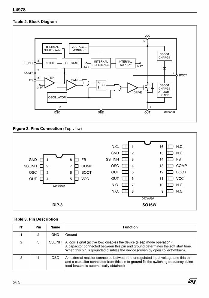
Table 2. Block Diagram
Figure 3. Pins Connection (Top view)
Table 3. Pin Description
N° Pin Name Function
1 2 GND Ground
2 3 SS_INH A logic signal (active low) disables the device (sleep mode operation). A capacitor connected between this pin and ground determines the soft start time. When this pin is grounded disables the device (driven by open collector/drain).
3 4 OSC An external resistor connected between the unregulated input voltage and this pin and a capacitor connected from this pin to ground fix the switching frequency. (Line feed forward is automatically obtained)
INHIBIT SOFTSTART
VOLTAGESMONITOR
THERMALSHUTDOWN
E/APWM
3.3V
OSCILLATOR
R
SQ
INTERNALREFERENCE
INTERNALSUPPLY
3.3V 5.1V
DRIVE
CBOOTCHARGE
CBOOTCHARGEAT LIGHTLOADS
2
7
8FB
COMP
SS_INH
3 1 4
6
5
BOOT
OSC GND OUT
VCC
D97IN594
GND
SS_INH
OSC
OUT
1
3
2
4 VCC
BOOT
COMP
FB8
7
6
5
D97IN595
N.C.
GND
SS_INH
OSC
OUT
N.C.
OUT
N.C. N.C.
N.C.
BOOT
VCC
COMP
FB
N.C.
N.C.1
3
2
4
5
6
7
8
14
13
12
11
10
9
15
16
D97IN596
DIP-8 SO16W
2/13
L4978
(*) Pins 1, 7, 8, 9, 10, 15 and 16 are not internally, electrically connected to the die.
Table 4. Thermal Data
(*) Package mounted on board.
Table 5. Absolute Maximum Ratings
4 5, 6 OUT Stepdown regulator output
5 11 VCC Unregulated DC input voltage
6 12 BOOT A capacitor connected between this pin and OUT allows to drive the internal DMOS Transistors
7 13 COMP E/A output to be used for frequency compensation
8 14 FB Stepdown feedback input. Connecting directly to this pin results in an output voltage of 3.3V. An external resistive divider is required for higher output voltages.
Symbol Parameter Minidip SO16 Unit
Rth(j-amb) Thermal Resistance Junction to ambient Max. 90 (*) 110 (*) °C/W
Symbol Parameter Value Unit
Minidip S016
V5 V11 Input voltage 58 V
V4 V5,V6 Output DC voltageOutput peak voltage at t = 0.1ms f=200KHz
-1-5
VV
I4 I5,I6 Maximum output current int. limit.
V6-V5 V12-V11 14 V
V6 V12 Bootstrap voltage 70 V
V7 V13 Analogs input voltage (VCC= 24V) 12 V
V2 V3 Analogs input voltage (VCC= 24V) 13 V V8 V14 (VCC= 20V) 6
-0.3
VV
Ptot Power dissipation a Tamb ≤ 60°CDIP-8SO16
10.8
WW
Tj,Tstg Junction and storage temperature -40 to 150 °C
Table 3. Pin Description (continued)
N° Pin Name Function
3/13
L4978
Table 6. Electrical Characteristcs(Tj = 25°C, Cosc = 2.7nF, Rosc = 20kΩ, VCC = 24V, unless otherwise specified). “" Specification Referredto Tj from 0 to 125°C
Symbol Parameter Test Condition Min. Typ. Max. Unit
DYNAMIC CHARACTERISTIC
VI Operating input voltage range Vo = 3.3 to 50V; Io = 2A 8 55 V
Vo Output voltage Io = 0.5A 3.33 3.36 3.39 V
Io = 0.2 to 2A Vcc = 8 to 55V
3.292 3.36 3.427 V 3.22 3.36 3.5 V
Vd Dropout voltage Vcc = 10V; Io = 2A 0.58 0.733 V 1.173 V
Il Maximum limiting current Vcc = 8 to 55V 2.5 3 3.5 A
Efficiency Vo = 3.3V; Io= 2A 87 %
fs Switching frequency 90 100 110 KHz
SVRR Supply voltage ripple rejection Vi = Vcc+2VRMS; Vo= Vref; Io = 2.5A; f ripple= 100Hz
60 dB
Switching Frequency Stability vs. Vcc
Vcc = 8 to 55V 3 6 %
Temp. stability of switching frequency
Tj = 0 to 125°C 4 %
SOFT START
Soft start charge current 30 40 50 µA
Soft start discharge current 6 10 14 µA
INHIBIT
VLL Low level voltage 0.9 V
IsLL Isource Low level 5 15 µA
DC CHARACTERISTICS
Iqop Total operating quiescent current
4 6 mA
Iq Quiescent current Duty Cycle = 0; VFB= 3.8V 2.5 3.5 mA
Iqst-by Total stand-by quiescent current
Vinh < 0.9V 100 200 µA
Vcc = 55V; Vinh<0.9V 150 300 µA
ERROR AMPLIFIER
VFB Voltage Feedback Input 3.33 3.36 3.39 V
RL Line regulation Vcc = 8 to 55V 5 10 mV
Ref. voltage stability vs temperature
0.4 mV/°C
VoH High level output voltage VFB = 2.5V 10.3 V
VoL Low level output voltage VFB = 3.8V 0.65 V
Io source Source output current Vcomp= 6V; VFB= 2.5V 180 220 µA
Io sink Sink output current Vcomp = 6V; VFB= 3.8V 200 300 µA
Ib Source bias current 2 3 µA
SVRR E/A Supply voltage ripple rejection Vcomp = VFB; Vcc = 8 to 55V 60 80 dB
DC open loop gain RL= ∞ 50 57 dB
gm Transconductance Icomp = -0.1 to 0.1mA Vcomp = 6V
2.5 mS
4/13
L4978
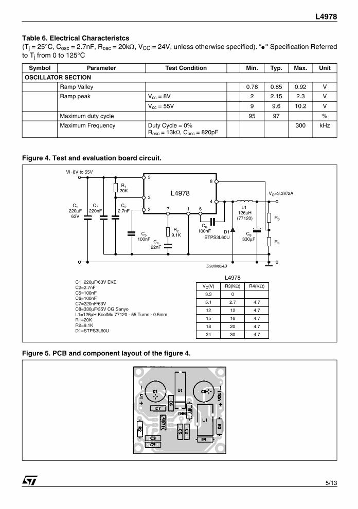
Figure 4. Test and evaluation board circuit.
Figure 5. PCB and component layout of the figure 4.
OSCILLATOR SECTION
Ramp Valley 0.78 0.85 0.92 V
Ramp peak Vcc = 8V 2 2.15 2.3 V
Vcc = 55V 9 9.6 10.2 V
Maximum duty cycle 95 97 %
Maximum Frequency Duty Cycle = 0% Rosc = 13kΩ, Cosc = 820pF
300 kHz
Table 6. Electrical Characteristcs(Tj = 25°C, Cosc = 2.7nF, Rosc = 20kΩ, VCC = 24V, unless otherwise specified). “" Specification Referredto Tj from 0 to 125°C
Symbol Parameter Test Condition Min. Typ. Max. Unit
D98IN834B
5
2
8
4
1
L4978
C1220µF63V
C8330µF
VO=3.3V/2A
Vi=8V to 55V
R120K
C22.7nF
R29.1K
C422nF
3
7 L1 126µH(77120)
6
D1STPS3L60U
C5100nF
C7220nF
C6100nF
R3
R4
C1=220µF/63V EKE C2=2.7nFC5=100nFC6=100nFC7=220nF/63VC8=330µF/35V CG SanyoL1=126µH KoolMu 77120 - 55 Turns - 0.5mmR1=20KR2=9.1KD1=STPS3L60U
VO(V) R3(KΩ) R4(KΩ)
3.3
5.1
12
15
18
24
0
2.7
12
16
20
30
4.7
4.7
4.7
4.7
4.7
L4978
5/13
L4978
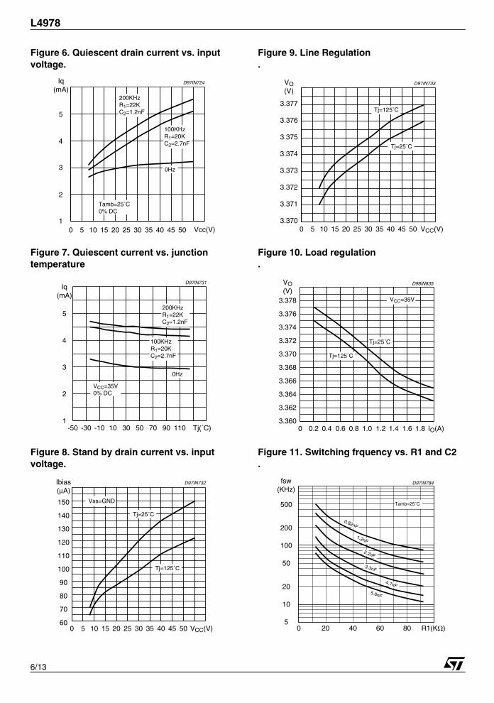
Figure 6. Quiescent drain current vs. input voltage.
Figure 7. Quiescent current vs. junction temperature
Figure 8. Stand by drain current vs. input voltage.
Figure 9. Line Regulation.
Figure 10. Load regulation.
Figure 11. Switching frquency vs. R1 and C2.
0 5 10 15 20 25 30 35 40 45 50 Vcc(V)1
2
3
4
5
Iq(mA)
200KHzR1=22KC2=1.2nF
0Hz
D97IN724
Tamb=25˚C0% DC
100KHzR1=20KC2=2.7nF
-50 -30 -10 10 30 50 70 90 110 Tj(˚C)1
2
3
4
5
Iq(mA)
D97IN731
0Hz
200KHzR1=22KC2=1.2nF
VCC=35V0% DC
100KHzR1=20KC2=2.7nF
0 5 10 15 20 25 30 35 40 45 50 VCC(V)60
70
80
90
100
110
120
130
140
150
Ibias(µA)
D97IN732
Tj=25˚C
Tj=125˚C
Vss=GND
0 5 10 15 20 25 30 35 40 45 50 VCC(V)3.370
3.371
3.372
3.373
3.374
3.375
3.376
3.377
VO(V)
D97IN733
Tj=25˚C
Tj=125˚C
0 0.2 0.4 0.6 1.0 1.2 1.4 1.6 IO(A)0.8 1.83.360
3.362
3.364
3.366
3.368
3.370
3.372
3.374
3.376
3.378
VO(V)
Tj=25˚C
Tj=125˚C
VCC=35V
D98IN835
0 20 40 60 80 R1(KΩ)5
10
20
50
100
200
500
fsw(KHz)
D97IN784
0.82nF
1.2nF
2.2nF
3.3nF
4.7nF
5.6nF
Tamb=25˚C
6/13
L4978
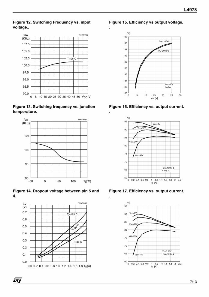
Figure 12. Switching Frequency vs. input voltage..
Figure 13. Switching frequency vs. junction temperature.
Figure 14. Dropout voltage between pin 5 and 4.
Figure 15. Efficiency vs output voltage..
Figure 16. Efficiency vs. output current..
Figure 17. Efficiency vs. output current..
0 5 10 15 20 25 30 35 40 45 50 VCC(V)90.0
92.5
95.0
97.5
100.0
102.5
105.0
107.5
fsw(KHz)
D97IN735
Tj=25˚C
-50 0 50 100 Tj(˚C)90
95
100
105
fsw(KHz)
D97IN785
0.0 0.2 0.4 0.6 0.8 1.0 1.2 1.4 IO(A)1.6 1.80.0
0.1
0.2
0.3
0.4
0.5
∆V(V)
0.6
0.7
Tj=25˚C
Tj=125˚C
D98IN836
Tj=-25˚C
0 5 10 15 20 25 3080
82
84
86
88
90
92
94
96
98
Vo [V]
[%]
fsw=100kHz
fsw=200kHz
Vcc=35VIo=2A
Vcc=12V
Vcc=8V
0 0.2 0.4 0.6 0.8 1 1.2 1.4 1.6 1.8 2 2.260
65
70
75
80
85
90
95
Io [A]
[%]
Vcc=8V
Vcc=12V
Vcc=24V
Vcc=48V
fsw=100kHzVo=5.1V
0 0.2 0.4 0.6 0.8 1 1.2 1.4 1.6 1.8 2 2.260
65
70
75
80
85
90
95
Io [A]
[%]
Vcc=8V
Vcc=12V
Vcc=24V
Vcc=48V
Vo=3.36V fsw=100kHz
7/13
L4978
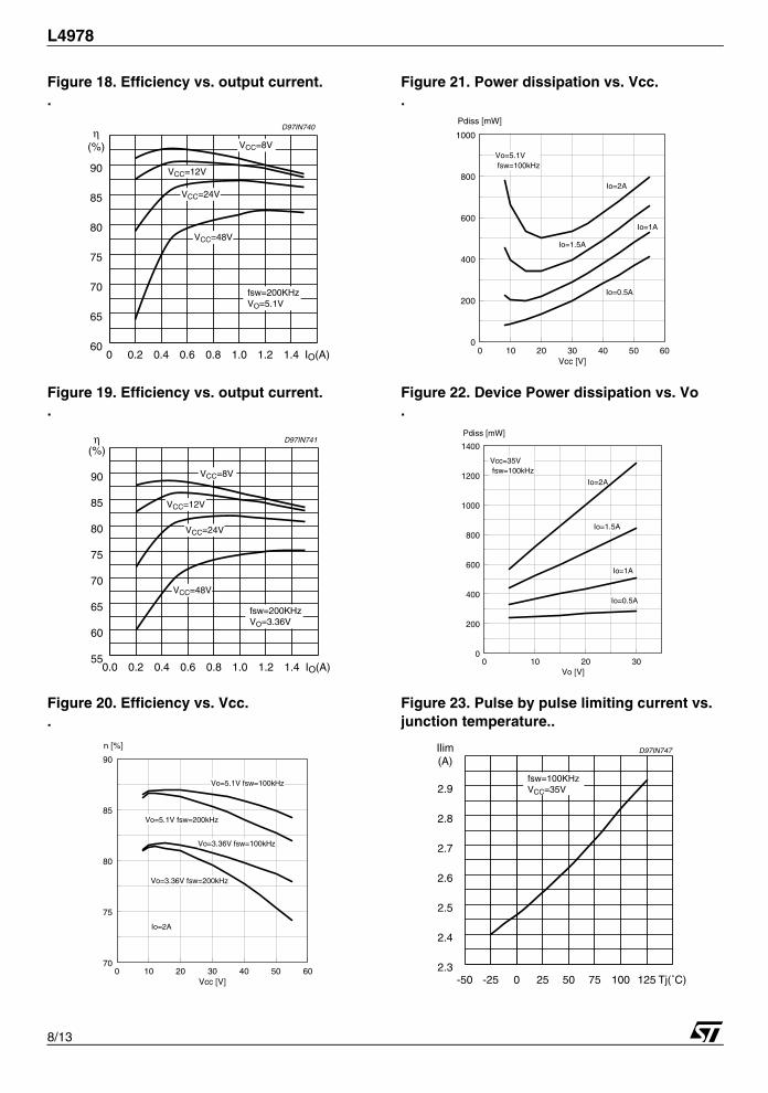
Figure 18. Efficiency vs. output current. .
Figure 19. Efficiency vs. output current. .
Figure 20. Efficiency vs. Vcc..
Figure 21. Power dissipation vs. Vcc..
Figure 22. Device Power dissipation vs. Vo.
Figure 23. Pulse by pulse limiting current vs. junction temperature..
0 0.2 0.4 0.6 0.8 1.0 1.2 1.4 IO(A)60
65
70
75
80
85
90
η(%)
D97IN740
VCC=8V
fsw=200KHzVO=5.1V
VCC=12V
VCC=24V
VCC=48V
0.0 0.2 0.4 0.6 0.8 1.0 1.2 1.4 IO(A)55
60
65
70
75
80
85
90
η(%)
D97IN741
VCC=8V
fsw=200KHzVO=3.36V
VCC=12V
VCC=24V
VCC=48V
Io=2A
0 10 20 30 40 50 6070
75
80
85
90
Vcc [V]
n [%]
Vo=5.1V fsw=100kHz
Vo=5.1V fsw=200kHz
Vo=3.36V fsw=100kHz
Vo=3.36V fsw=200kHz
Io=0.5A
Io=2A
Io=1A
0 10 20 30 40 50 600
200
400
600
800
1000
Vcc [V]
Pdiss [mW]
Io=1.5A
Vo=5.1V fsw=100kHz
Io=2A
Io=1A
0 10 20 300
200
400
600
800
1000
1200
1400
Vo [V]
Pdiss [mW]
Io=0.5A
Io=1.5A
Vcc=35V fsw=100kHz
-50 -25 0 25 50 75 100 125 Tj(˚C)2.3
2.4
2.5
2.6
2.7
2.8
2.9
Ilim(A)
D97IN747
fsw=100KHzVCC=35V
8/13
L4978
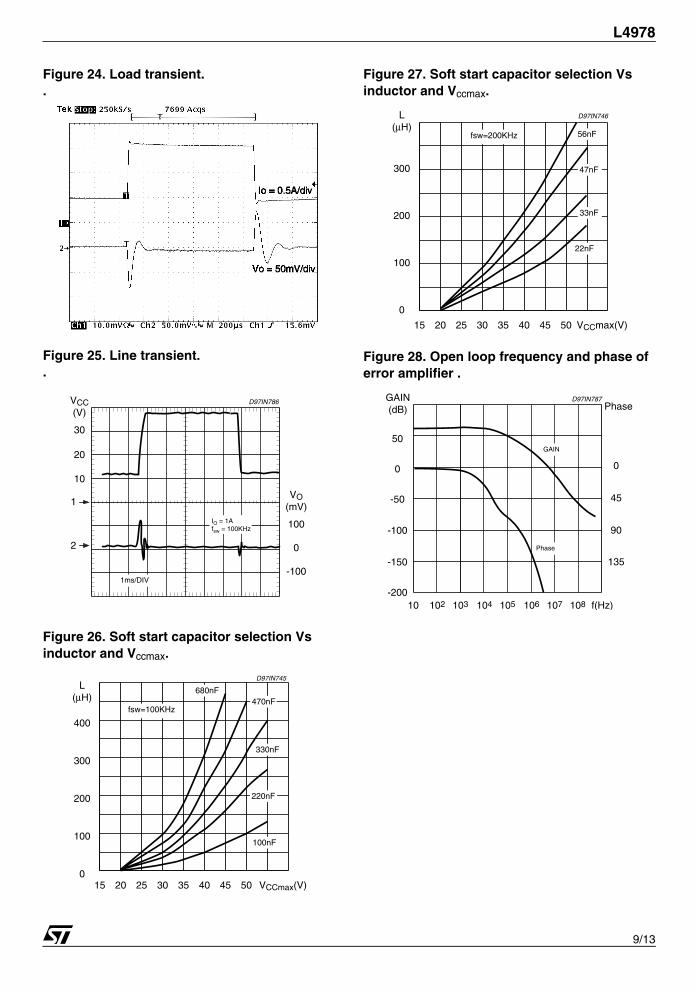
Figure 24. Load transient. .
Figure 25. Line transient. .
Figure 26. Soft start capacitor selection Vs inductor and Vccmax.
Figure 27. Soft start capacitor selection Vs inductor and Vccmax.
Figure 28. Open loop frequency and phase of error amplifier .
2
1
D97IN786VCC(V)
30
20
10
VO(mV)
100
0
-1001ms/DIV
IO = 1Afsw = 100KHz
15 20 25 30 35 40 45 50 VCCmax(V)0
100
200
300
400
L(µH)
D97IN745
680nF
fsw=100KHz470nF
330nF
220nF
100nF
15 20 25 30 35 40 45 50 VCCmax(V)
0
100
200
300
L(µH)
56nFfsw=200KHz
D97IN746
47nF
33nF
22nF
10 103 105 107 f(Hz)102 104 106 108-200
-150
-100
-50
GAIN(dB)
0
50
Phase
0
45
90
135
D97IN787
GAIN
Phase
9/13
L4978
3 Package Informations
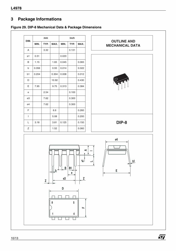
Figure 29. DIP-8 Mechanical Data & Package Dimensions
OUTLINE ANDMECHANICAL DATA
DIM.mm inch
MIN. TYP. MAX. MIN. TYP. MAX.
A 3.32 0.131
a1 0.51 0.020
B 1.15 1.65 0.045 0.065
b 0.356 0.55 0.014 0.022
b1 0.204 0.304 0.008 0.012
D 10.92 0.430
E 7.95 9.75 0.313 0.384
e 2.54 0.100
e3 7.62 0.300
e4 7.62 0.300
F 6.6 0.260
I 5.08 0.200
L 3.18 3.81 0.125 0.150
Z 1.52 0.060
DIP-8
10/13
L4978
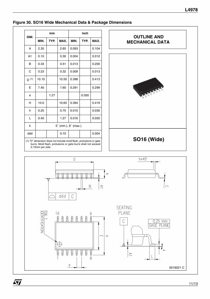
Figure 30. SO16 Wide Mechanical Data & Package Dimensions
OUTLINE ANDMECHANICAL DATA
DIM.mm inch
MIN. TYP. MAX. MIN. TYP. MAX.
A 2.35 2.65 0.093 0.104
A1 0.10 0.30 0.004 0.012
B 0.33 0.51 0.013 0.200
C 0.23 0.32 0.009 0.013
D (1) 10.10 10.50 0.398 0.413
E 7.40 7.60 0.291 0.299
e 1.27 0.050
H 10.0 10.65 0.394 0.419
h 0.25 0.75 0.010 0.030
L 0.40 1.27 0.016 0.050
k 0˚ (min.), 8˚ (max.)
ddd 0.10 0.004
(1) “D” dimension does not include mold flash, protusions or gateburrs. Mold flash, protusions or gate burrs shall not exceed0.15mm per side.
SO16 (Wide)
0016021 C
11/13
L4978
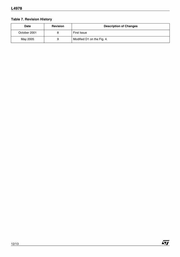
Table 7. Revision History
Date Revision Description of Changes
October 2001 8 First Issue
May 2005 9 Modified D1 on the Fig. 4.
12/13

Information furnished is believed to be accurate and reliable. However, STMicroelectronics assumes no responsibility for the consequencesof use of such information nor for any infringement of patents or other rights of third parties which may result from its use. No license is grantedby implication or otherwise under any patent or patent rights of STMicroelectronics. Specifications mentioned in this publication are subjectto change without notice. This publication supersedes and replaces all information previously supplied. STMicroelectronics products are notauthorized for use as critical components in life support devices or systems without express written approval of STMicroelectronics.
The ST logo is a registered trademark of STMicroelectronics.All other names are the property of their respective owners
© 2005 STMicroelectronics - All rights reserved
STMicroelectronics group of companiesAustralia - Belgium - Brazil - Canada - China - Czech Republic - Finland - France - Germany - Hong Kong - India - Israel - Italy - Japan -
Malaysia - Malta - Morocco - Singapore - Spain - Sweden - Switzerland - United Kingdom - United States of Americawww.st.com
13/13
L4978