3-phase brushless fan motor driver -...
TRANSCRIPT
Product structure : Semiconductor IC This product is not designed protection against radioactive rays .
1/19 TSZ02201-0828AB400090-1-2© 2013 ROHM Co., Ltd. All rights reserved.
22.FEB.2013 Rev.001TSZ22111 · 14 · 001
http://www.rohm.com
For air-conditioner fan motor 3-Phase Brushless Fan Motor Driver BM6202FS
General Description
This motor driver IC adopts PrestoMOS™ as the output transistor, and put in a small full molding package with the high voltage gate driver chip. The protection circuits for overcurrent, overheating, under voltage lock out and the high voltage bootstrap diode with current regulation are built-in. It provides optimum motor drive system for a wide variety of applications by the combination with controller BD6201X series and enables motor unit standardization.
Features 600V PrestoMOS™ built-in Output current 1.5A Bootstrap operation by floating high side driver
(including diode) 3.3V logic input compatible Protection circuits provided: OCP, TSD and UVLO Fault output (open drain)
Applications Air conditioners; air cleaners; water pumps;
dishwashers; washing machines General OA equipment
Key Specifications Output MOSFET voltage: 600V Driver output current (DC): ±1.5A(Max.) Driver output current (Pulse): ±2.5A(Max.) Output MOSFET DC on resistance: 2.7Ω (Typ.) Operating case temperature: -20°C to +100°C Junction temperature: +150°C Power dissipation: 3.0W
Package W (Typ.) x D (Typ.) x H (Max.)
SSOP-A54_23 22.0 mm x 14.1 mm x 2.4 mm
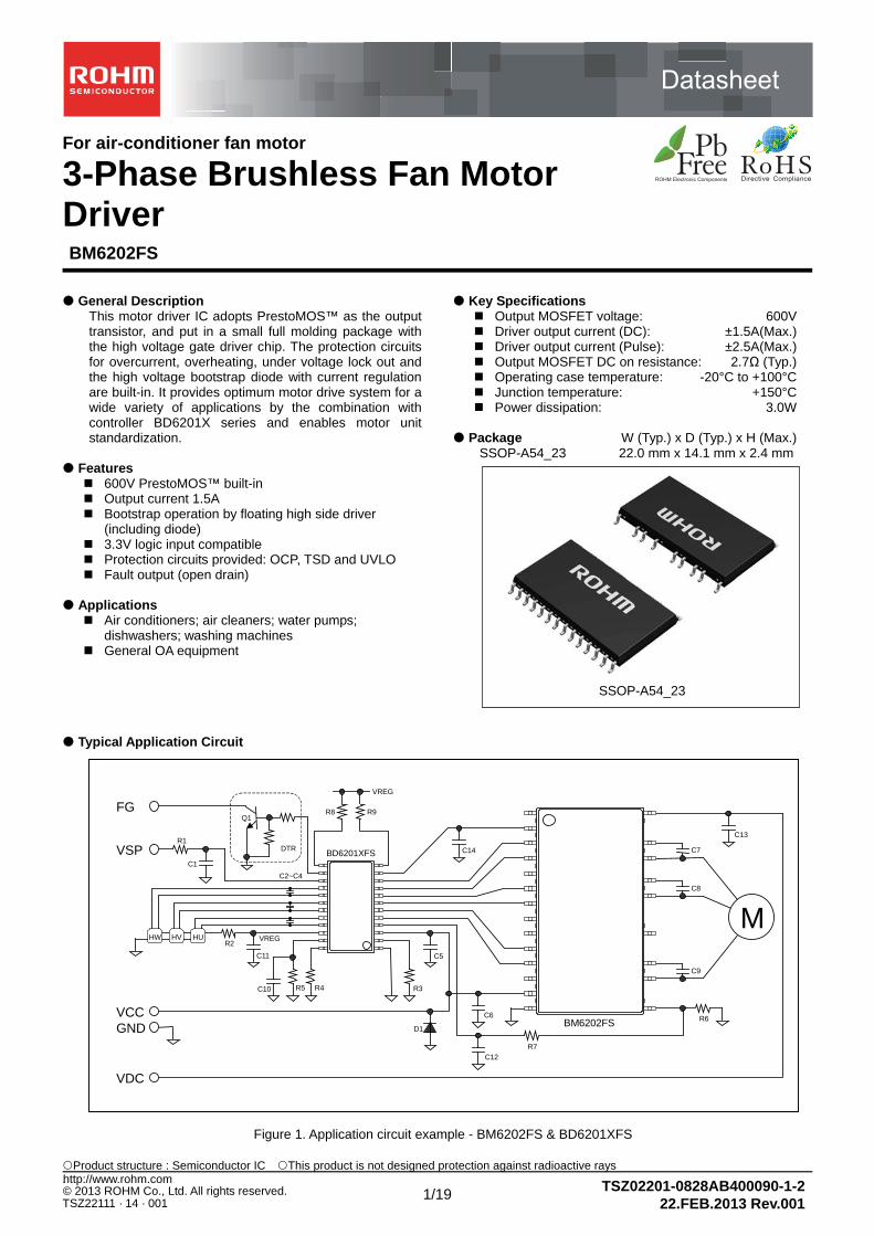
Typical Application Circuit
SSOP-A54_23
Figure 1. Application circuit example - BM6202FS & BD6201XFS
R8 R9
VREG
VREG C5
HU HV HW
VSP
FG
DTR
VCC GND
M
VDC
BD6201XFS
BM6202FS
R1
R2
R3R4 R5
R6
R7
Q1
C1 C2~C4
C6
C7
C8
C9 C10
C11
C12
C13
D1
C14

2/19
DatasheetDatasheetBM6202FS
TSZ02201-0828AB400090-1-2© 2013 ROHM Co., Ltd. All rights reserved. 22.FEB.2013 Rev.001
http://www.rohm.com
TSZ22111 · 15 · 001
Block Diagram and Pin Configuration Figure 2. Block diagram Figure 3. Pin configuration Pin Descriptions (NC: No Connection)
Pin Name Function Pin Name Function
1 VCC Low voltage power supply 23 VDC High voltage power supply
2 FOB Fault signal output (open drain) - VDC
3 UH Phase U high side control input 22 BU Phase U floating power supply
4 UL Phase U low side control input - U
5 NC 21 U Phase U output
6 VH Phase V high side control input 20 BV Phase V floating power supply
7 VL Phase V low side control input - V
8 NC 19 V Phase V output
9 NC - VDC
10 WH Phase W high side control input 18 VDC High voltage power supply
11 WL Phase W low side control input 17 BW Phase W floating power supply
12 FOB Fault signal output (open drain) - W
13 VCC Low voltage power supply 16 W Phase W output
14 GND Ground 15 PGND Ground (current sense pin) Note) All pin cut surfaces visible from the side of package are no connected, except the pin number is expressed as a “-”.
VCC
FOB
UH
UL
VH
VL
WH
WL
FOB
VCC
GND PGND
W
BW
VDC
V
BV
U
BU
VDC
PGND
LEVEL SHIFT &
GATE DRIVER
BU
U
M
22
21
1 VCC
GND
VDC
3 UH
4 UL
BV
V
20
19
6 VH
7 VL
BW
W
17
16
10 WH
11 WL
2 FOB
12 FOB
13 VCC
VDC
15
14
FAULT
SDB
LEVEL SHIFT &
GATE DRIVER
FAULT
SDB
LEVEL SHIFT &
GATE DRIVER
FAULT
SDB
TRIP
18 VDC
VCC
23
FAULT
TRIP
TRIP

3/19
DatasheetDatasheetBM6202FS
TSZ02201-0828AB400090-1-2© 2013 ROHM Co., Ltd. All rights reserved. 22.FEB.2013 Rev.001
http://www.rohm.com
TSZ22111 · 15 · 001
Functional Descriptions 1) Control input pins (UH, UL, VH, VL, WH, WL)
The input threshold voltages of the control pins are 2.5V and 0.8V, with a hysteresis voltage of approximately 0.4V. The IC will accept input voltages up to the VCC voltage. When the same phase control pins are input high at the same time, the high side and low side gate driver outputs become low. Dead time is installed in the control signals. The control input pins are connected internally to pull-down resistors (100kΩ nominal). However, the switching noise on the output stage may affect the input on these pins and cause undesired operation. In such cases, attaching an external pull-down resistor (10kΩ recommended) between each control pin and ground, or connecting each pin to an input voltage of 0.8V or less (preferably GND), is recommended.
2) Under voltage lock out (UVLO) circuit
To secure the lowest power supply voltage necessary to operate the driver, and to prevent under voltage malfunctions, the UVLO circuits are independently built into the upper side floating driver and the lower side driver. When the supply voltage falls to VUVL or below, the controller forces driver outputs low. When the voltage rises to VUVH or above, the UVLO circuit ends the lockout operation and returns the chip to normal operation. Even if the controller returns to normal operation, the output begins from the following control input signal.
Figure 4. Low voltage monitor - UVLO - timing chart
Truth table
HIN LIN HO LO
L L L L
H L H L
L H L H
H H Inhibition
Note) HIN: UH,VH,WH, LIN: UL,VL,WL
VCC
HIN
LIN
HO
LO
VB
HIN
LIN
HO
LO
VCCUVH
VCCUVL
VBUVH
VBUVL

4/19
DatasheetDatasheetBM6202FS
TSZ02201-0828AB400090-1-2© 2013 ROHM Co., Ltd. All rights reserved. 22.FEB.2013 Rev.001
http://www.rohm.com
TSZ22111 · 15 · 001
3) Bootstrap operation Figure 5. Charging period Figure 6. Discharging period
The bootstrap is operated by the charge period and the discharge period being alternately repeated for bootstrap capacitor (CB) as shown in the figure above. In a word, this operation is repeated while the output of an external transistor is switching with synchronous rectification. Because the supply voltage of the floating driver is charged from the VCC power supply to CB through prevention of backflow diode DX, it is approximately (VCC-1V). The resistance series connection with DX has the impedance of approximately 200 Ω. The capacitance value for the bootstrap is the following formula:
Example: Floating driver power supply quiescence current IBBQ : 150µA(max.) Bootstrap diode reverse bias current ILBD : 10µA(max.) Carrier frequency FPWM : 20kHz Output MOSFET total gate charge Qg : 25nC(max.) Floating driver transmission loss QLOSS : 1nC(max.) Drop voltage of the floating driver power supply dVDROP : 3V CBOOT » (( IBBQ + ILBD ) / FPWM + 2 x Qg + QLOSS ) / dVDROP ≈ 20nF
The allowed drop voltage actually becomes smaller by the range of the used power supply voltage, the output MOSFET ON resistance, the forward voltages of the internal boot diode (the drop voltage to the capacitor by the charge current), and the power supply voltage monitor circuits etc. Please set the calculation value to the criterion about the capacitance value tenfold or more to secure the margin in consideration of temperature characteristics and the value change, etc. Moreover, the example of the mentioned above assumes the synchronous rectification switching. Because the total gate charge is needed only by the carrier frequency in the upper switching section, for example 150° commutation driving, it becomes a great capacity shortage in the above settings. Please set it after confirming actual application operation.
4) Thermal shutdown (TSD) circuit
The TSD circuit operates when the junction temperature of the gate driver exceeds the preset temperature (150°C nominal). At this time, the controller forces all driver outputs low. Since thermal hysteresis is provided in the TSD circuit, the chip returns to normal operation when the junction temperature falls below the preset temperature (125°C nominal). The TSD circuit is designed only to shut the IC off to prevent thermal runaway. It is not designed to protect the IC or guarantee its operation in the presence of extreme heat. Do not continue using the IC after the TSD circuit is activated, and do not use the IC in an environment where activation of the circuit is assumed. Moreover, it is not possible to follow the output MOSFET junction temperature rising rapidly because it is a gate driver chip that monitors the temperature and it is likely not to function effectively.
5) Overcurrent protection (OCP) circuit
The overcurrent protection circuit can be activated by connecting a low value resistor for current detection between the PGND pin and the GND pin. When the PGND pin voltage reaches or surpasses the threshold value (0.9V typical), the gate driver outputs low to the gate of all output MOSFETs, thus initiating the overcurrent protection operation.
CB HO
VS
VDC VB
L
H
DX
LO
OFF
ON
VCC
CB HO
VS
VDC VB
H
L
DX
LO
ON
OFF
VCC

5/19
DatasheetDatasheetBM6202FS
TSZ02201-0828AB400090-1-2© 2013 ROHM Co., Ltd. All rights reserved. 22.FEB.2013 Rev.001
http://www.rohm.com
TSZ22111 · 15 · 001
6) Fault signal output When the gate driver detects either state that should be protected (UVLO / TSD / OCP), the FOB pin outputs low (open drain) for at least 25µs nominal. The FOB pin has wired-OR connection with each phase gate driver chip internally, and into another phase also entering the protection operation. Even when this function is not used, the FOB pin is pull-up to the voltage of 3V or more and at least a resistor with a value 10k Ω or more. Moreover, the signal from the outside of the chip is not passed because of the built-in analog filter, but the internal control signals (UVLO / TSD / OCP) pass the filter (2.0µs Min.) for the malfunction prevention by the switching noise, etc.
Figure 7. Fault signal bi-directional input pin interface
Figure 8. Fault operation ~ OCP ~ timing chart The release time from the protection operation can be changed by inserting an external capacitor. Refer to the formula below. Release time of 2ms or more is recommended.
Figure 9. Release time setting application circuit Figure 10. Release time (reference data @R=100kΩ)
2.0 t = - ln ( 1 -
VPU ) · R · C [s]
HIN
LIN
PGND
HO
LO
FOB
0.9V(typ.) 2.0µs (Min.)
25µs (Typ.)
2.0µs (Min.)
25µs (Typ.)
FOB SHUTDOWN
TSD
OCP
UVLO
FILTER
FAULT
FOB
VPU
R
C
0
1
2
3
4
5
6
7
8
9
10
0.01 0.10 1.00
Capacitance : C[µF]
Rel
ease
tim
e : t
[ms]
VPU=5V VPU=15V

6/19
DatasheetDatasheetBM6202FS
TSZ02201-0828AB400090-1-2© 2013 ROHM Co., Ltd. All rights reserved. 22.FEB.2013 Rev.001
http://www.rohm.com
TSZ22111 · 15 · 001
FOB
VREG
FIB
BD6201XFS BM6202FS
100k
C
When using controller BD6201X series as a control IC, the FOB pin can be linked to the external fault signal input pin of the side of the control IC since it has the internal pull-up resistor. Refer to figure 11. Figure 11. Interface equivalent circuit
7) Switching time Figure 12. Switching time definition
Parameter Symbol Reference Unit Conditions
tdH(on) 930 ns
trH 170 ns
trrH 250 ns
tdH(off) 600 ns
High side switching time
tfH 20 ns
tdL(on) 990 ns
trL 220 ns
trrL 250 ns
tdL(off) 600 ns
Low side switching time
tfL 60 ns
VDC=300V, VCC=15V, ID=0.75A VIN= 0V↔5V, Inductive load
XH, XL
VDS
ID
ton
td(on) tr
trr
td(off)
toff
tf
10%
90%
10%
90%

7/19
DatasheetDatasheetBM6202FS
TSZ02201-0828AB400090-1-2© 2013 ROHM Co., Ltd. All rights reserved. 22.FEB.2013 Rev.001
http://www.rohm.com
TSZ22111 · 15 · 001
Absolute Maximum Ratings (Ta=25°C)
Ratings Parameter Symbol
BM6202FS Unit
Output MOSFET VDSS 600*1 V
Supply voltage VDC -0.3 to 600*1 V
Output voltage VU, VV, VW -0.3 to 600*1 V
High side supply pin voltage VBU, VBV, VBW -0.3 to 600*1 V
High side floating supply voltage VBU-VU, VBV-VV, VBW-VW -0.3 to 20 V
Low side supply voltage VCC -0.3 to 20 V
All others VI/O -0.3 to VCC V
Driver outputs (DC) IOMAX(DC) ±1.5*2 A
Driver outputs (Pulse) IOMAX(PLS) ±2.5*2 A
Fault signal output IOMAX(FOB) 15*1 mA
Power dissipation Pd 3.00*3 W
Thermal resistance Rthj-c 15 °C/W
Operating case temperature TC -20 to 100 °C
Storage temperature TSTG -55 to 150 °C
Junction temperature Tjmax 150 °C
Note) All voltages are with respect to ground. *1 Do not, however, exceed Pd or ASO. *2 Pw ≤ 10µs, Duty cycle ≤ 1% *3 Mounted on a 70mm x 70mm x 1.6mm FR4 glass-epoxy board with less than 3% copper foil. Derated at 24mW/°C above 25°C.
Operating Conditions (Tc=25°C)
Range Parameter Symbol
Min. Typ. Max. Unit
Supply voltage VDC - 310 400 V
High side floating supply voltage VBU-VU, VBV-VV, VBW-VW 13.5 15 16.5 V
Low side supply voltage VCC 13.5 15 16.5 V
Minimum input pulse width TMIN 0.8 - - µs
Dead time TDT 1.5 - - µs
Shunt resistor (PGND) RS 0.4 - - Ω
Junction temperature Tj - - 125 °C
Note) All voltages are with respect to ground.

8/19
DatasheetDatasheetBM6202FS
TSZ02201-0828AB400090-1-2© 2013 ROHM Co., Ltd. All rights reserved. 22.FEB.2013 Rev.001
http://www.rohm.com
TSZ22111 · 15 · 001
Electrical Characteristics (Unless otherwise specified, Ta=25°C and VCC=15V)
Limits Parameter Symbol
Min. Typ. Max. Unit Conditions
Power supply
HS quiescence current IBBQ 30 70 150 µA XH=XL=L, each phase
LS quiescence current ICCQ 0.4 0.9 1.5 mA XH=XL=L
Output MOSFET
D-S breakdown voltage V(BR)DSS 600 - - V ID=1mA, XH=XL=L
Leak current IDSS - - 100 µA VDS=600V, XH=XL=L
DC on resistance RDS(ON) - 2.7 3.5 Ω ID=0.75A
Diode forward voltage VSD - 1.1 1.5 V ID=0.75A
Bootstrap diode
Leak current ILBD - - 10 µA VBX=600V
Forward voltage VFBD 1.5 1.8 2.1 V IBD=-5mA, including series-R
Series resistance RBD - 200 - Ω
Control inputs
Input bias current IXIN 30 50 70 µA VIN=5V
Input high voltage VXINH 2.5 - VCC V
Input low voltage VXINL 0 - 0.8 V
Under voltage lock out
HS release voltage VBUVH 9.5 10.0 10.5 V VBX - VX
HS lockout voltage VBUVL 8.5 9.0 9.5 V VBX - VX
LS release voltage VCCUVH 11.0 11.5 12.0 V
LS lockout voltage VCCUVL 10.0 10.5 11.0 V
Overcurrent protection
Threshold voltage VSNS 0.8 0.9 1.0 V
Fault output
Output low voltage VFOL - - 0.8 V IO=+10mA
Input high voltage VFINH 2.5 - VCC V
Input low voltage VFINL 0 - 0.8 V
Noise masking time TMASK 2.0 - - µs

9/19
DatasheetDatasheetBM6202FS
TSZ02201-0828AB400090-1-2© 2013 ROHM Co., Ltd. All rights reserved. 22.FEB.2013 Rev.001
http://www.rohm.com
TSZ22111 · 15 · 001
Typical Performance Curves (Reference data)
20
40
60
80
100
120
12 14 16 18 20
Supply Voltage : VBX-VX [V]
Sup
ply
Cur
rent
: IQ
VB
X [
µA
] _
125°C25°C
-25°C1.0
1.5
2.0
2.5
3.0
12 14 16 18 20
Supply Voltage : VCC [V]
Sup
ply
Cur
rent
: Ic
c [m
A]
125°C25°C
-25°C
0.0
0.5
1.0
1.5
2.0
12 14 16 18 20
Supply Voltage : VCC [V]
Sup
ply
Cur
rent
: Ic
c [m
A]
125°C25°C
-25°C
Figure 15. Low side drivers operating current Figure 16. Quiescence current (FPWM: 20kHz, two phase switching) (High side driver, each phase)
Figure 13. Quiscence current Figure 14. Low side drivers operating current (Low side drivers) (FPWM: 20kHz, one phase switching)
0.0
0.5
1.0
1.5
2.0
12 14 16 18 20
Supply Voltage : VCC [V]
Sup
ply
Cur
rent
: Ic
c [m
A]
125°C25°C
-25°C
10/19
DatasheetDatasheetBM6202FS
TSZ02201-0828AB400090-1-2© 2013 ROHM Co., Ltd. All rights reserved. 22.FEB.2013 Rev.001
http://www.rohm.com
TSZ22111 · 15 · 001
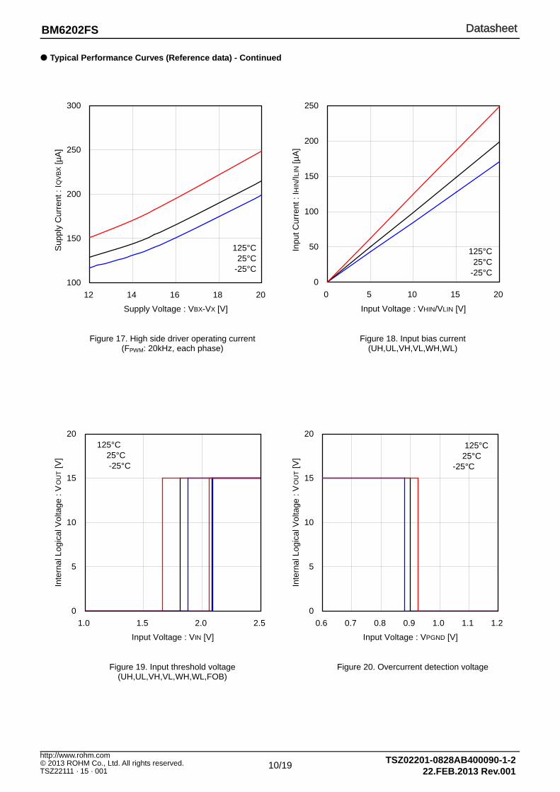
Typical Performance Curves (Reference data) - Continued
0
5
10
15
20
1.0 1.5 2.0 2.5
Input Voltage : VIN [V]
Inte
rnal
Log
ical
Vol
tage
: V
OU
T [
V]
125°C 25°C -25°C
Figure 19. Input threshold voltage Figure 20. Overcurrent detection voltage (UH,UL,VH,VL,WH,WL,FOB)
Figure 17. High side driver operating current Figure 18. Input bias current (FPWM: 20kHz, each phase) (UH,UL,VH,VL,WH,WL)
100
150
200
250
300
12 14 16 18 20
Supply Voltage : VBX-VX [V]
Sup
ply
Cur
rent
: IQ
VB
X [
µA
] _
125°C25°C
-25°C
0
50
100
150
200
250
0 5 10 15 20
Input Voltage : VHIN/VLIN [V]
Inpu
t Cur
rent
: IH
IN/I
LIN
[µ
A]
_
125°C25°C
-25°C
0
5
10
15
20
0.6 0.7 0.8 0.9 1.0 1.1 1.2
Input Voltage : VPGND [V]
Inte
rnal
Log
ical
Vol
tage
: V
OU
T [
V]
125°C 25°C-25°C

11/19
DatasheetDatasheetBM6202FS
TSZ02201-0828AB400090-1-2© 2013 ROHM Co., Ltd. All rights reserved. 22.FEB.2013 Rev.001
http://www.rohm.com
TSZ22111 · 15 · 001
Typical Performance Curves (Reference data) - Continued Figure 23. Release time Figure 24. Fault output ON resistance
(No external capacitor)
Figure 21. Thermal shut down Figure 22. Noise masking time
0
5
10
15
20
100 110 120 130 140 150 160 170 180
Junction Temperature : Tj [°C]
Inte
rnal
Log
ical
Vol
tage
: V
OU
T [
V]
0
2
4
6
8
-25 0 25 50 75 100 125
Junction Temperature : Tj [°C]
Noi
se M
aski
ng T
ime
: TM
AS
K [
µs]
TSDUVLOOCP
0
10
20
30
40
50
-25 0 25 50 75 100 125
Junction Temperature : Tj [°C]
Rel
ease
Tim
e : T
RE
LE
AS
E [
µs]
TSDUVLOOCP
0.0
0.2
0.4
0.6
0.8
1.0
0 2 4 6 8 10
Output Current : IFOB [mA]
Out
put V
olta
ge :
VF
OB [
V]
125°C25°C
-25°C

12/19
DatasheetDatasheetBM6202FS
TSZ02201-0828AB400090-1-2© 2013 ROHM Co., Ltd. All rights reserved. 22.FEB.2013 Rev.001
http://www.rohm.com
TSZ22111 · 15 · 001
Typical Performance Curves (Reference data) - Continued Figure 27. Minimum input pulse width Figure 28. Input/Output propagation delay
Figure 25. Under voltage lock out Figure 26. Under voltage lock out (High side driver, each phase) (Low side drivers)
0
5
10
15
20
8 9 10 11 12 13
Supply Voltage : VCC [V]
Inte
rnal
Log
ical
Out
put V
olta
ge :
VO
UT [
V]
125°C 25°C-25°C
125°C 25°C-25°C
0
500
1000
1500
12 13 14 15 16 17 18
Supply Voltage : VCC [V]
Inpu
t/Out
put P
ropa
gatio
n D
elay
: T
d [n
s]
Solid : Low sideDashed : High side
Td(on)
Td(off)
0
500
1000
1500
12 13 14 15 16 17 18
Supply Voltage : VCC [V]
Min
imum
Inpu
t Pul
se W
idth
: T
PW
min
[ns
] Solid : Low sideDashed : High side
0
5
10
15
20
8 9 10 11 12 13
Supply Voltage : VBX - VX [V]
Inte
rnal
Log
ical
Vol
tage
: V
OU
T [
V]
125°C 25°C-25°C
125°C 25°C-25°C

13/19
DatasheetDatasheetBM6202FS
TSZ02201-0828AB400090-1-2© 2013 ROHM Co., Ltd. All rights reserved. 22.FEB.2013 Rev.001
http://www.rohm.com
TSZ22111 · 15 · 001
Typical Performance Curves (Reference data) - Continued Figure 31. Bootstrap diode forward voltage Figure 32. Bootstrap series resistor
Figure 29. Output MOSFET ON resistance Figure 30. Output MOSFET body diode
0
2
4
6
8
0.0 0.5 1.0 1.5 2.0
Drain Current : IDS [A]
Out
put O
n R
esis
tanc
e : R
DS
ON
[ohm
]
125°C25°C
-25°C
0.0
0.5
1.0
1.5
2.0
0.0 0.5 1.0 1.5 2.0
Source Current : ISD [A]
For
war
d V
olta
ge :
VS
D [
V]
-25°C25°C
125°C
0.0
0.2
0.4
0.6
0.8
1.0
1.2
0 2 4 6 8 10
Bootstrap Diode Current : IBD [mA]
For
war
d V
olta
ge :
VF
BD
[V
]
-25°C25°C
125°C
0
1
2
3
4
0 2 4 6 8 10
Bootstrap Series Resistor Current : IBR [mA]
Vo
ltag
e :
VB
OO
TR [
V]
125°C25°C
-25°C

14/19
DatasheetDatasheetBM6202FS
TSZ02201-0828AB400090-1-2© 2013 ROHM Co., Ltd. All rights reserved. 22.FEB.2013 Rev.001
http://www.rohm.com
TSZ22111 · 15 · 001
Typical Performance Curves (Reference data) - Continued Figure 35. Low side switching loss Figure 36. Low side recovery loss
(VDC=300V) (VDC=300V)
Figure 33. High side switching loss Figure 34. High side recovery loss (VDC=300V) (VDC=300V)
0
50
100
150
200
0.0 0.5 1.0 1.5
Drain Current : IO [A]
E [
µJ]
125°C25°C
-25°CEON
EOFF
0
5
10
15
0.0 0.5 1.0 1.5
Drain Current : IO [A]
E [
µJ]
-25°C25°C
125°C
0
50
100
150
200
0.0 0.5 1.0 1.5
Drain Current : IO [A]
E [
µJ]
125°C25°C
-25°C EON
EOFF
0
5
10
15
0.0 0.5 1.0 1.5
Drain Current : IO [A]
E [
µJ]
-25°C25°C
125°C

15/19
DatasheetDatasheetBM6202FS
TSZ02201-0828AB400090-1-2© 2013 ROHM Co., Ltd. All rights reserved. 22.FEB.2013 Rev.001
http://www.rohm.com
TSZ22111 · 15 · 001
Application Circuit Example
Figure 37. Application circuit example (150° commutation driver)
Parts list Parts Value Manufacturer Type Parts Value Ratings Type
IC1 - ROHM BM6202FS C1 0.1µF 50V Ceramic
IC2 - ROHM BD62012FS C2~4 2200pF 50V Ceramic
R1 1kΩ ROHM MCR18EZPF1001 C5 10µF 50V Ceramic
R2 150Ω ROHM MCR18EZPJ151 C6 10µF 50V Ceramic
R3 22kΩ ROHM MCR18EZPF2202 C7~9 1µF 50V Ceramic
R4 100kΩ ROHM MCR18EZPF1003 C10 0.1µF 50V Ceramic
R5 100kΩ ROHM MCR18EZPF1003 C11 1µF 50V Ceramic
R6 0.5Ω ROHM MCR50JZHFL1R50 x 3 C12 100pF 50V Ceramic
R7 10kΩ ROHM MCR18EZPF1002 C13 0.1µF 630V Ceramic
R8 0Ω ROHM MCR18EZPJ000 C14 0.1µF 50V Ceramic
R9 0Ω ROHM MCR18EZPJ000 HX - - Hall elements
Q1 - ROHM DTC124EUA
D1 - ROHM KDZ20B
R8 R9
VREG
VREG C5
HU HV HW
VSP
FG
DTR
VCC GND
M
VDC
IC2
IC1
R1
R2
R3R4 R5
R6
R7
Q1
C1 C2~C4
C6
C7
C8
C9 C10
C11
C12
C13
D1
C14

16/19
DatasheetDatasheetBM6202FS
TSZ02201-0828AB400090-1-2© 2013 ROHM Co., Ltd. All rights reserved. 22.FEB.2013 Rev.001
http://www.rohm.com
TSZ22111 · 15 · 001
Interfaces Figure 38. UH, UL, VH, VL, WH, WL Figure 39. PGND Figure 40. FOB Figure 41. VCC, GND, VDC, BX(BU/BV/BW), X(U/V/W)
VREG
100k
VH
VL
UH
UL
WH
WL
PGND
VREG
FOB
VCC
GND
X
BX
PGND
VDC

17/19
DatasheetDatasheetBM6202FS
TSZ02201-0828AB400090-1-2© 2013 ROHM Co., Ltd. All rights reserved. 22.FEB.2013 Rev.001
http://www.rohm.com
TSZ22111 · 15 · 001
Notes for Use 1) Absolute maximum ratings
Devices may be destroyed when supply voltage or operating temperature exceeds the absolute maximum rating. Because the cause of this damage cannot be identified as, for example, a short circuit or an open circuit, it is important to consider circuit protection measures, such as adding fuses, if any value in excess of absolute maximum ratings is to be implemented.
2) Electrical potential at GND
Keep the GND terminal to the minimum potential under any operating condition. In addition, check to determine whether there is any terminal that provides voltage below GND, including the voltage during transient phenomena. However, note that even if the voltage does not fall below GND in any other operating condition, it can still swing below GND potential when the motor generates back electromotive force at the PGND pin. The chip layout in this product is designed to avoid this sort of electrical potential problem, but pulling excessive current may still result in malfunctions. Therefore, it is necessary to observe operation closely to conclusively confirm that there is no problem in actual operation. If there are a small signal GND and a high current GND, it is recommended to separate the patterns for the high current GND and the small signal GND and provide a proper grounding to the reference point of the set not to affect the voltage at the small signal GND with the change in voltage due to resistance component of pattern wiring and high current. Also for GND wiring pattern of the component externally connected, pay special attention not to cause undesirable change to it.
3) High voltage terminal – VDC, BU/U, BV/V and BW/W
When using this IC, the high voltage terminals VDC, BU/U, BV/V and BW/W need a resin coating between these pins. It is judged that the inter-pins distance is not enough. If any special mode in excess of absolute maximum ratings is to be implemented with this product or its application circuits, it is important to take physical safety measures, such as providing voltage-clamping diodes or fuses. And, set the output transistor so that it does not exceed absolute maximum ratings or ASO. In the event a large capacitor is connected between the output and ground, and if VCC and VDC are short-circuited with 0V or ground for any reason, the current charged in the capacitor flows into the output and may destroy the IC.
4) Power supply lines
Return current generated by the motor’s Back-EMF requires countermeasures, such as providing a return current path by inserting capacitors across the power supply and GND (10µF, ceramic capacitor is recommended). In this case, it is important to conclusively confirm that none of the negative effects sometimes seen with electrolytic capacitors including a capacitance drop at low temperatures occurs. Also, the connected power supply must have sufficient current absorbing capability. Otherwise, the regenerated current will increase voltage on the power supply line, which may in turn cause problems with the product, including peripheral circuits exceeding the absolute maximum rating. To help protect against damage or degradation, physical safety measures should be taken, such as providing a voltage-clamping diode across the power supply and GND.
5) Thermal design
Use a thermal design that allows sufficient margin in light of the power dissipation (Pd) in actual operating conditions. 6) Inter-pin shorts and mounting errors
Take caution when positioning the IC for mounting on printed circuit boards. The IC may be damaged if there is any connection error or if pins are shorted together. Also, connecting the power supply in reverse polarity can damage the IC. Take precautions against reverse polarity when connecting the power supply lines, such as establishing an external diode between the power supply and the IC power supply pin.
7) Operation in strong electromagnetic fields
Using this product in strong electromagnetic fields may cause IC malfunctions. Take extreme caution with electromagnetic fields.
8) Testing on application boards
When testing the IC on an application board, connecting a capacitor to a low impedance pin subjects the IC to stress. Always discharge capacitors after each process or step. Always turn the IC's power supply off before connecting it to or removing it from a jig or fixture during the inspection process. Ground the IC during assembly steps as an antistatic measure. Use similar precaution when transporting or storing the IC.
9) Regarding the input pin of the IC
Do not force voltage to the input pins when the power does not supply to the IC. Also, do not force voltage to the input pins that exceed the supply voltage or in the guaranteed the absolute maximum rating value even if the power is supplied to the IC.

18/19
DatasheetDatasheetBM6202FS
TSZ02201-0828AB400090-1-2© 2013 ROHM Co., Ltd. All rights reserved. 22.FEB.2013 Rev.001
http://www.rohm.com
TSZ22111 · 15 · 001
Ordering Information Physical Dimension, Tape and Reel Information Marking Diagram
B M 6 2 0 2 F S - E 2
ROHM Part Number BM6202 : 600V/1.5A
Package FS : SSOP-A54_23
Packaging specification E2 : Embossed taping
BM6202FS
1PIN MARK LOT No.
PRODUCT NAME SSOP-A54_23 (TOP VIEW)
1
1.6 0.1
14.1
0.
3
22.0 0.1
0.27 0.1
0.38 0.1
(MAX 22.35 include BURR)
11.4
0.
2
2.1
0.1 1.
050.
1 0
.1
14
1523
SSOP-A54_23

19/19
DatasheetDatasheetBM6202FS
TSZ02201-0828AB400090-1-2© 2013 ROHM Co., Ltd. All rights reserved. 22.FEB.2013 Rev.001
http://www.rohm.com
TSZ22111 · 15 · 001
Revision History
Date Revision Changes
22.FEB.2013 001 New release

DatasheetDatasheet
Notice - GE Rev.002© 2014 ROHM Co., Ltd. All rights reserved.
Notice Precaution on using ROHM Products
1. Our Products are designed and manufactured for application in ordinary electronic equipments (such as AV equipment, OA equipment, telecommunication equipment, home electronic appliances, amusement equipment, etc.). If you intend to use our Products in devices requiring extremely high reliability (such as medical equipment (Note 1), transport equipment, traffic equipment, aircraft/spacecraft, nuclear power controllers, fuel controllers, car equipment including car accessories, safety devices, etc.) and whose malfunction or failure may cause loss of human life, bodily injury or serious damage to property (“Specific Applications”), please consult with the ROHM sales representative in advance. Unless otherwise agreed in writing by ROHM in advance, ROHM shall not be in any way responsible or liable for any damages, expenses or losses incurred by you or third parties arising from the use of any ROHM’s Products for Specific Applications.
(Note1) Medical Equipment Classification of the Specific Applications JAPAN USA EU CHINA
CLASSⅢ CLASSⅢ
CLASSⅡb CLASSⅢ
CLASSⅣ CLASSⅢ
2. ROHM designs and manufactures its Products subject to strict quality control system. However, semiconductor
products can fail or malfunction at a certain rate. Please be sure to implement, at your own responsibilities, adequate safety measures including but not limited to fail-safe design against the physical injury, damage to any property, which a failure or malfunction of our Products may cause. The following are examples of safety measures:
[a] Installation of protection circuits or other protective devices to improve system safety [b] Installation of redundant circuits to reduce the impact of single or multiple circuit failure
3. Our Products are designed and manufactured for use under standard conditions and not under any special or extraordinary environments or conditions, as exemplified below. Accordingly, ROHM shall not be in any way responsible or liable for any damages, expenses or losses arising from the use of any ROHM’s Products under any special or extraordinary environments or conditions. If you intend to use our Products under any special or extraordinary environments or conditions (as exemplified below), your independent verification and confirmation of product performance, reliability, etc, prior to use, must be necessary:
[a] Use of our Products in any types of liquid, including water, oils, chemicals, and organic solvents [b] Use of our Products outdoors or in places where the Products are exposed to direct sunlight or dust [c] Use of our Products in places where the Products are exposed to sea wind or corrosive gases, including Cl2,
H2S, NH3, SO2, and NO2
[d] Use of our Products in places where the Products are exposed to static electricity or electromagnetic waves [e] Use of our Products in proximity to heat-producing components, plastic cords, or other flammable items [f] Sealing or coating our Products with resin or other coating materials [g] Use of our Products without cleaning residue of flux (even if you use no-clean type fluxes, cleaning residue of
flux is recommended); or Washing our Products by using water or water-soluble cleaning agents for cleaning residue after soldering
[h] Use of the Products in places subject to dew condensation
4. The Products are not subject to radiation-proof design. 5. Please verify and confirm characteristics of the final or mounted products in using the Products. 6. In particular, if a transient load (a large amount of load applied in a short period of time, such as pulse. is applied,
confirmation of performance characteristics after on-board mounting is strongly recommended. Avoid applying power exceeding normal rated power; exceeding the power rating under steady-state loading condition may negatively affect product performance and reliability.
7. De-rate Power Dissipation (Pd) depending on Ambient temperature (Ta). When used in sealed area, confirm the actual
ambient temperature. 8. Confirm that operation temperature is within the specified range described in the product specification. 9. ROHM shall not be in any way responsible or liable for failure induced under deviant condition from what is defined in
this document.
Precaution for Mounting / Circuit board design 1. When a highly active halogenous (chlorine, bromine, etc.) flux is used, the residue of flux may negatively affect product
performance and reliability. 2. In principle, the reflow soldering method must be used; if flow soldering method is preferred, please consult with the
ROHM representative in advance. For details, please refer to ROHM Mounting specification

DatasheetDatasheet
Notice - GE Rev.002© 2014 ROHM Co., Ltd. All rights reserved.
Precautions Regarding Application Examples and External Circuits 1. If change is made to the constant of an external circuit, please allow a sufficient margin considering variations of the
characteristics of the Products and external components, including transient characteristics, as well as static characteristics.
2. You agree that application notes, reference designs, and associated data and information contained in this document
are presented only as guidance for Products use. Therefore, in case you use such information, you are solely responsible for it and you must exercise your own independent verification and judgment in the use of such information contained in this document. ROHM shall not be in any way responsible or liable for any damages, expenses or losses incurred by you or third parties arising from the use of such information.
Precaution for Electrostatic
This Product is electrostatic sensitive product, which may be damaged due to electrostatic discharge. Please take proper caution in your manufacturing process and storage so that voltage exceeding the Products maximum rating will not be applied to Products. Please take special care under dry condition (e.g. Grounding of human body / equipment / solder iron, isolation from charged objects, setting of Ionizer, friction prevention and temperature / humidity control).
Precaution for Storage / Transportation 1. Product performance and soldered connections may deteriorate if the Products are stored in the places where:
[a] the Products are exposed to sea winds or corrosive gases, including Cl2, H2S, NH3, SO2, and NO2 [b] the temperature or humidity exceeds those recommended by ROHM [c] the Products are exposed to direct sunshine or condensation [d] the Products are exposed to high Electrostatic
2. Even under ROHM recommended storage condition, solderability of products out of recommended storage time period may be degraded. It is strongly recommended to confirm solderability before using Products of which storage time is exceeding the recommended storage time period.
3. Store / transport cartons in the correct direction, which is indicated on a carton with a symbol. Otherwise bent leads
may occur due to excessive stress applied when dropping of a carton. 4. Use Products within the specified time after opening a humidity barrier bag. Baking is required before using Products of
which storage time is exceeding the recommended storage time period.
Precaution for Product Label QR code printed on ROHM Products label is for ROHM’s internal use only.
Precaution for Disposition When disposing Products please dispose them properly using an authorized industry waste company.
Precaution for Foreign Exchange and Foreign Trade act Since our Products might fall under controlled goods prescribed by the applicable foreign exchange and foreign trade act, please consult with ROHM representative in case of export.
Precaution Regarding Intellectual Property Rights 1. All information and data including but not limited to application example contained in this document is for reference
only. ROHM does not warrant that foregoing information or data will not infringe any intellectual property rights or any other rights of any third party regarding such information or data. ROHM shall not be in any way responsible or liable for infringement of any intellectual property rights or other damages arising from use of such information or data.:
2. No license, expressly or implied, is granted hereby under any intellectual property rights or other rights of ROHM or any
third parties with respect to the information contained in this document.
Other Precaution 1. This document may not be reprinted or reproduced, in whole or in part, without prior written consent of ROHM. 2. The Products may not be disassembled, converted, modified, reproduced or otherwise changed without prior written
consent of ROHM. 3. In no event shall you use in any way whatsoever the Products and the related technical information contained in the
Products or this document for any military purposes, including but not limited to, the development of mass-destruction weapons.
4. The proper names of companies or products described in this document are trademarks or registered trademarks of
ROHM, its affiliated companies or third parties.

DatasheetDatasheet
Notice – WE Rev.001© 2014 ROHM Co., Ltd. All rights reserved.
General Precaution 1. Before you use our Pro ducts, you are requested to care fully read this document and fully understand its contents.
ROHM shall n ot be in an y way responsible or liabl e for fa ilure, malfunction or acci dent arising from the use of a ny ROHM’s Products against warning, caution or note contained in this document.
2. All information contained in this docume nt is current as of the issuing date and subj ect to change without any prior
notice. Before purchasing or using ROHM’s Products, please confirm the la test information with a ROHM sale s representative.
3. The information contained in this doc ument is provi ded on an “as is” basis and ROHM does not warrant that all
information contained in this document is accurate an d/or error-free. ROHM shall not be in an y way responsible or liable for any damages, expenses or losses incurred by you or third parties resulting from inaccuracy or errors of or concerning such information.