3220 ieeetransactions on industrial electronics, … · with bcm control. interestingly, the...
TRANSCRIPT

3220 IEEE TRANSACTIONS ON INDUSTRIAL ELECTRONICS, VOL. 61, NO. 7, JULY 2014
Boundary Conduction Mode Controlled Power FactorCorrector With Line Voltage Recovery and TotalHarmonic Distortion Improvement Techniques
Yi-Ping Su, Student Member, IEEE, Chia-Lung Ni, Chun-Yen Chen, Yi-Ting Chen,Jen-Chieh Tsai, and Ke-Horng Chen, Senior Member, IEEE
Abstract—The proposed line voltage recovery (LVR) and thetotal harmonic distortion improvement (THDI) technique improvepower factor (PF) and total harmonic distortion (THD) over awide line voltage range in boundary conduction mode controlledpower factor corrector (PFC). The LVR detects the input lineroot-mean-square voltage to generate the digital equivalent codeto the THDI for optimizing the THD by tuning the on-time value atdifferent line voltages. In addition, the LVR and the THDI providea feedforward path to reduce the ripple of the feedback voltagefor further improving the THD. Therefore, the PFC controller cankeep high PF and low THD over a wide line voltage. Experimentalresults demonstrate that the peak PF value is 0.998 and theminimum THD is 1.7% by the test circuit fabricated in a TSMC800-V ultrahigh-voltage process with the universal line voltagerange of 90–264 V.
Index Terms—Line voltage recovery (LVR), power factor (PF),total harmonic distortion (THD).
I. INTRODUCTION
G REEN POWER becomes more important in the worlddue to the lack of energy. In green power designs, high-
quality ac power conversion aims to enhance power utilizationefficiency of the ac power supply, minimize power loss, and im-prove regulation. For increasing the power utilization efficiencyof the ac power supply, the demanded power factor correction(PFC) converter can shape the input current of offline powersupplies to be in phase with the line voltage. In addition, thetotal harmonic distortion (THD) of the line current, which alsodetermines the quality of power source, is expressed in Fig. 1and the following equation:
THD =
(cos2 θ
PF2 − 1
)1/2
(1)
where power factor PF is the ratio of the real power to theapparent power, and θ is the phase angle between the linecurrent and voltage.
Manuscript received December 12, 2012; revised March 25, 2013, May 25,2013, and July 13, 2013; accepted August 13, 2013. Date of publicationSeptember 10, 2013; date of current version January 31, 2014.
Y.-P. Su, C.-L. Ni, C.-Y. Chen, Y.-T. Chen, and J.-C. Tsai are with theMixed-Signal and Power Management IC Laboratory, Institute of ElectricalEngineering, National Chiao Tung University, Hsinchu 300, Taiwan.
K.-H. Chen is with the Department of Electrical Engineering, National ChiaoTung University, Hsinchu 300, Taiwan (e-mail: [email protected]).
Color versions of one or more of the figures in this paper are available onlineat http://ieeexplore.ieee.org.
Digital Object Identifier 10.1109/TIE.2013.2281302
Fig. 1. Diagram of THD versus PF.
Fig. 2. Two major THD-deteriorated contributors in the conventional PFCwith BCM control.
Interestingly, the relationship between PF and THD revealsthat THD is still poor even if PF is high. That is to say,for high-quality power supply, both the PF and the THD areimportant. The harmonic currents will increase power losses onthe transmission line and cause electrical equipment damages.Therefore, the THD needs to be decreased for high-qualitypower supply even if the PF is high. There are safety standardsthat determine the maximum THD of electrical products inmany countries, such as EN61000-3-2. In other words, im-proving THD becomes an essential requirement for electricalproducts.
Basically, two major THD-deteriorated contributors areshown in Fig. 2 in a conventional PFC boost converter withboundary conduction mode (BCM) control [1]–[3]. One is thecrossover distortion caused by the forward voltage of the diodesin the bridge and parasitic capacitances Ctotal, which includesthe parasitic capacitance of D3 and power nMOSFET. Theother is the line frequency reflected distortion. The frequency
0278-0046 © 2013 IEEE. Personal use is permitted, but republication/redistribution requires IEEE permission.See http://www.ieee.org/publications_standards/publications/rights/index.html for more information.
SU et al.: BOUNDARY CONDUCTION MODE CONTROLLED PFC WITH LVR AND THDI TECHNIQUES 3221
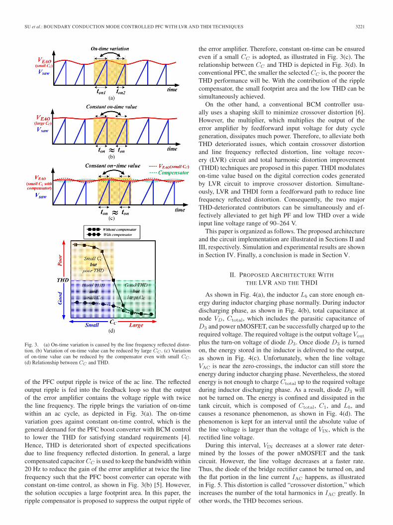
Fig. 3. (a) On-time variation is caused by the line frequency reflected distor-tion. (b) Variation of on-time value can be reduced by large CC . (c) Variationof on-time value can be reduced by the compensator even with small CC .(d) Relationship between CC and THD.
of the PFC output ripple is twice of the ac line. The reflectedoutput ripple is fed into the feedback loop so that the outputof the error amplifier contains the voltage ripple with twicethe line frequency. The ripple brings the variation of on-timewithin an ac cycle, as depicted in Fig. 3(a). The on-timevariation goes against constant on-time control, which is thegeneral demand for the PFC boost converter with BCM controlto lower the THD for satisfying standard requirements [4].Hence, THD is deteriorated short of expected specificationsdue to line frequency reflected distortion. In general, a largecompensated capacitor CC is used to keep the bandwidth within20 Hz to reduce the gain of the error amplifier at twice the linefrequency such that the PFC boost converter can operate withconstant on-time control, as shown in Fig. 3(b) [5]. However,the solution occupies a large footprint area. In this paper, theripple compensator is proposed to suppress the output ripple of
the error amplifier. Therefore, constant on-time can be ensuredeven if a small CC is adopted, as illustrated in Fig. 3(c). Therelationship between CC and THD is depicted in Fig. 3(d). Inconventional PFC, the smaller the selected CC is, the poorer theTHD performance will be. With the contribution of the ripplecompensator, the small footprint area and the low THD can besimultaneously achieved.
On the other hand, a conventional BCM controller usu-ally uses a shaping skill to minimize crossover distortion [6].However, the multiplier, which multiplies the output of theerror amplifier by feedforward input voltage for duty cyclegeneration, dissipates much power. Therefore, to alleviate bothTHD deteriorated issues, which contain crossover distortionand line frequency reflected distortion, line voltage recov-ery (LVR) circuit and total harmonic distortion improvement(THDI) techniques are proposed in this paper. THDI modulateson-time value based on the digital correction codes generatedby LVR circuit to improve crossover distortion. Simultane-ously, LVR and THDI form a feedforward path to reduce linefrequency reflected distortion. Consequently, the two majorTHD-deteriorated contributors can be simultaneously and ef-fectively alleviated to get high PF and low THD over a wideinput line voltage range of 90–264 V.
This paper is organized as follows. The proposed architectureand the circuit implementation are illustrated in Sections II andIII, respectively. Simulation and experimental results are shownin Section IV. Finally, a conclusion is made in Section V.
II. PROPOSED ARCHITECTURE WITH
THE LVR AND THE THDI
As shown in Fig. 4(a), the inductor Lb can store enough en-ergy during inductor charging phase normally. During inductordischarging phase, as shown in Fig. 4(b), total capacitance atnode VD, Ctotal, which includes the parasitic capacitance ofD3 and power nMOSFET, can be successfully charged up to therequired voltage. The required voltage is the output voltage Vout
plus the turn-on voltage of diode D3. Once diode D3 is turnedon, the energy stored in the inductor is delivered to the output,as shown in Fig. 4(c). Unfortunately, when the line voltageVAC is near the zero-crossings, the inductor can still store theenergy during inductor charging phase. Nevertheless, the storedenergy is not enough to charge Ctotal up to the required voltageduring inductor discharging phase. As a result, diode D3 willnot be turned on. The energy is confined and dissipated in thetank circuit, which is composed of Ctotal, C1, and Lb, andcauses a resonance phenomenon, as shown in Fig. 4(d). Thephenomenon is kept for an interval until the absolute value ofthe line voltage is larger than the voltage of VIN, which is therectified line voltage.
During this interval, VIN decreases at a slower rate deter-mined by the losses of the power nMOSFET and the tankcircuit. However, the line voltage decreases at a faster rate.Thus, the diode of the bridge rectifier cannot be turned on, andthe flat portion in the line current IAC happens, as illustratedin Fig. 5. This distortion is called “crossover distortion,” whichincreases the number of the total harmonics in IAC greatly. Inother words, the THD becomes serious.

3222 IEEE TRANSACTIONS ON INDUSTRIAL ELECTRONICS, VOL. 61, NO. 7, JULY 2014
Fig. 4. (a) Charging phase of the PFC boost converter. (b) Discharging phaseof the PFC boost converter. (c) Energy charges to the output when the linevoltage is high enough. (d) Energy is confined in the resonant tank when theline voltage is near zero-crossings.
Fig. 5. Line voltage and current waveforms of crossover distortionphenomenon.
If the inequality shown in (2) is simply conformed, it meansthat the energy stored in the charging phase is not high enoughto conduct diode D3 in the discharging phase
1
2Lb ·
[√2IAC,rms sin(π − φd)
]2≤ 1
2Ctotal · (Vout + Vdiode)
2
(2)
Fig. 6. Waveforms of the line current with (a) low line RMS voltage and(b) high line RMS voltage.
where φd is the crossover distortion angle, which indicates thatIAC starts away from the ideal sinusoidal wave; Vdiode is theforward voltage of D3; and IAC,rms is the RMS value of theline current.
Here, IAC,rms can be expressed as (3) based on the relation-ship between power and current. VAC,rms and PAC,rms are theRMS values of the line voltage and input power, respectively,i.e.,
IAC,rms =PAC,rms
VAC,rms. (3)
The limiting current Ilimit, which is defined as the requiredcurrent that can charge Ctotal up to the required voltage, isderived as (4). If the line current is lower than Ilimit, thecrossover distortion, which results in the flat portion in the linecurrent, will happen, i.e.,
Ilimit =
√Ctotal
Lb· (Vout + Vdiode). (4)
Using the information of the line voltage to modulate the on-time value of the power nMOSFET can alleviate crossover dis-tortion [7]. At a high level of the line voltage, the on-time valueis slightly shortened. Contrarily, the on-time value is extendedat the region of low line voltage near the zero-crossings. There-fore, the inductor current near the zero-crossings is increased tobreak through Ilimit. The THD performance can be improvedby compressing the flat portions.
However, good THD performance for universal input linevoltage is unable to be achieved if the modulated on-time valueis not adapted to the variation of the input line RMS voltage.With fixed output power, higher input line RMS voltage resultsin lower line current and larger flat portion, as depicted inFig. 6(a). On the contrary, lower input line RMS voltage resultsin higher line current and smaller flat portion, as depicted in

SU et al.: BOUNDARY CONDUCTION MODE CONTROLLED PFC WITH LVR AND THDI TECHNIQUES 3223
Fig. 7. Proposed BCM architecture with LVR and THDI.
Fig. 8. Circuit implementation of the proposed LVR circuit.
Fig. 9. Detailed operation waveform of the proposed LVR.
Fig. 6(b). The period of the flat portion, i.e., Tf , which resultsfrom the crossover distortion, is shown as
Tf =φd
2π · fline≈
√2
4· Ilimit · VAC,rms
fline · PAC,rms(5)
where
φd ≈√2
2· Ilimit ·
VAC,rms
PAC,rms
where fline is the line frequency. When the line RMS voltageis high, the crossover distortion becomes serious. Thus, the
Fig. 10. Circuit implementation of the debounce circuit.
crossover distortion needs to be adaptively improved accordingto different line RMS voltages such that the THD can bemaintained within a quite low level.
In addition, even if the modulated value of the on-time makesthe flat portion becomes shorter gradually, the waveform of theline current is unlike the ideal sinusoid waveform and, thus,may distort the line current [8]. Thus, the level of the modulatedon-time value has to be carefully designed at different linevoltages to get good THD performance.
Fig. 7 shows the architecture of the proposed PFC boostconverter, which is operating in BCM control in low-powerapplications. LVR can detect the input line RMS voltage togenerate the digital correction codes, namely, S90, S110, S220,and S264, to THDI for optimizing the THD by tuning the

3224 IEEE TRANSACTIONS ON INDUSTRIAL ELECTRONICS, VOL. 61, NO. 7, JULY 2014
Fig. 11. Schematic of the ZCD and the THDI technique.
Fig. 12. (a) Control mechanism of a conventional PFC controller. (b) Controlmechanism of the proposed PFC controller with the THDI technique.
on-time value at different line RMS voltages. In addition, LVRand THDI provide a feedforward path to reduce the ripple ofthe feedback voltage for decreasing THD. Therefore, high PFand low THD can be concurrently achieved over a wide rangeof the line voltage by the proposed method.
III. CIRCUIT IMPLEMENTATION
A. Proposed LVR Circuit
According to different line voltages, the THD should beimproved by different on-time values. In general, the peakvalue of the rectified line voltage VIN can indicate the RMSline voltage. In [9], one resistive divider is used to detect the
Fig. 13. Relationship between the THD and the mirror ratio at different lineRMS voltages.
Fig. 14. Relationship between the diode current and the output voltage.
input line RMS voltage. Although the method can detect theinput line RMS voltage successfully, it needs extra pins anddiscrete devices such that the efficiency is deteriorated andthe cost increases. The proposed LVR circuit in Fig. 8 canuse the inductor current sensing signal VCS, which is used forover inductor current protection originally, to reconstruct thesinusoidal-wave tendency of the line voltage and judge the inputline RMS voltage. Since the LVR does not need extra pinsand discrete resisters, the power consumption and cost can bereduced.
SU et al.: BOUNDARY CONDUCTION MODE CONTROLLED PFC WITH LVR AND THDI TECHNIQUES 3225
Fig. 15. Ripple of the feedback voltage and the output ripple of the erroramplifier with and without the proposed ripple compensator.
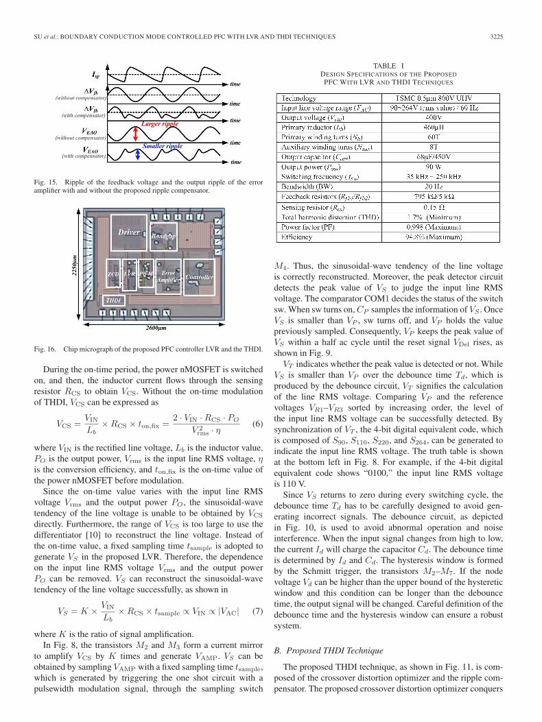
Fig. 16. Chip micrograph of the proposed PFC controller LVR and the THDI.
During the on-time period, the power nMOSFET is switchedon, and then, the inductor current flows through the sensingresistor RCS to obtain VCS. Without the on-time modulationof THDI, VCS can be expressed as
VCS =VIN
Lb×RCS × ton,fix =
2 · VIN ·RCS · PO
V 2rms · η
(6)
where VIN is the rectified line voltage, Lb is the inductor value,PO is the output power, Vrms is the input line RMS voltage, ηis the conversion efficiency, and ton,fix is the on-time value ofthe power nMOSFET before modulation.
Since the on-time value varies with the input line RMSvoltage Vrms and the output power PO, the sinusoidal-wavetendency of the line voltage is unable to be obtained by VCS
directly. Furthermore, the range of VCS is too large to use thedifferentiator [10] to reconstruct the line voltage. Instead ofthe on-time value, a fixed sampling time tsample is adopted togenerate VS in the proposed LVR. Therefore, the dependenceon the input line RMS voltage Vrms and the output powerPO can be removed. VS can reconstruct the sinusoidal-wavetendency of the line voltage successfully, as shown in
VS = K × VIN
Lb×RCS × tsample ∝ VIN ∝ |VAC| (7)
where K is the ratio of signal amplification.In Fig. 8, the transistors M2 and M3 form a current mirror
to amplify VCS by K times and generate VAMP. VS can beobtained by sampling VAMP with a fixed sampling time tsample,which is generated by triggering the one shot circuit with apulsewidth modulation signal, through the sampling switch
TABLE IDESIGN SPECIFICATIONS OF THE PROPOSED
PFC WITH LVR AND THDI TECHNIQUES
M4. Thus, the sinusoidal-wave tendency of the line voltageis correctly reconstructed. Moreover, the peak detector circuitdetects the peak value of VS to judge the input line RMSvoltage. The comparator COM1 decides the status of the switchsw. When sw turns on, CP samples the information of VS . OnceVS is smaller than VP , sw turns off, and VP holds the valuepreviously sampled. Consequently, VP keeps the peak value ofVS within a half ac cycle until the reset signal VDel rises, asshown in Fig. 9.VT indicates whether the peak value is detected or not. While
VS is smaller than VP over the debounce time Td, which isproduced by the debounce circuit, VT signifies the calculationof the line RMS voltage. Comparing VP and the referencevoltages VR1–VR3 sorted by increasing order, the level ofthe input line RMS voltage can be successfully detected. Bysynchronization of VT , the 4-bit digital equivalent code, whichis composed of S90, S110, S220, and S264, can be generated toindicate the input line RMS voltage. The truth table is shownat the bottom left in Fig. 8. For example, if the 4-bit digitalequivalent code shows “0100,” the input line RMS voltageis 110 V.
Since VS returns to zero during every switching cycle, thedebounce time Td has to be carefully designed to avoid gen-erating incorrect signals. The debounce circuit, as depictedin Fig. 10, is used to avoid abnormal operation and noiseinterference. When the input signal changes from high to low,the current Id will charge the capacitor Cd. The debounce timeis determined by Id and Cd. The hysteresis window is formedby the Schmitt trigger, the transistors M2–M7. If the nodevoltage Vd can be higher than the upper bound of the hystereticwindow and this condition can be longer than the debouncetime, the output signal will be changed. Careful definition of thedebounce time and the hysteresis window can ensure a robustsystem.
B. Proposed THDI Technique
The proposed THDI technique, as shown in Fig. 11, is com-posed of the crossover distortion optimizer and the ripple com-pensator. The proposed crossover distortion optimizer conquers

3226 IEEE TRANSACTIONS ON INDUSTRIAL ELECTRONICS, VOL. 61, NO. 7, JULY 2014
Fig. 17. (a) Simulation waveforms of the LVR circuit. (b) Zoom-inwaveforms.
two major drawbacks for THD improvement in [2] and [3].First, the requirement of extra resistors for on-time modulationdeteriorates the efficiency of the PFC boost converter. Second,the THD performance cannot be ensured with different lineRMS voltages.
The proposed crossover distortion optimizer alleviates thecrossover distortion at different line RMS voltages withoutextra pin and discrete devices. Instead, the zero-current detec-tion (ZCD) circuit, which is essential for the BCM control, isutilized. When the power nMOSFET is turned on, the voltageof ZCD node VZCD is shown as
VZCD = −VIN ·Naux
Nb(8)
where Nb and Naux are the primary and auxiliary windingturns, respectively.
The transistors M1–M3 and the resistors R1 and R2 of theZCD circuit form a negative feedback to clamp the voltage ofthe ZD pin to be VZD,clamp, which is higher than 0 V when thepower nMOSFET is turned on. Therefore, the current IZD canbe expressed as
IZD =VZD,clamp − VZD
RZD=
VZD,clamp + VIN·Naux
Nb
RZD. (9)
Fig. 18. Measured waveforms of the ZCD circuit at the input line RMSvoltages of (a) 110 V and (b) 220 V.
Fortunately, IZD includes the line voltage information. Thatis, a high line voltage produces larger IZD. Contrarily, alow line voltage produces smaller IZD. The THDI techniquemirrors IZD to modulate the on-time value of the powernMOSFET under four different input line RMS voltages. Asthe LVR detects the level of the input line RMS voltage,only one switch among M3–M16 will be turned on, and theselected current Iopt will charge the Vsaw to adjust the on-time value. Therefore, the slope of Vsaw is proportional tothe line voltage, owing to the dependence of Iopt on the linevoltage.
As shown in Fig. 12(a), serious crossover distortion withlarge flat portion happens in conventional PFC with constanton-time control. Since the power delivered to output in oneac line cycle is fixed with constant load condition, the outputpower can be manipulated within an ac line cycle. In otherwords, if the on-time at high Vin decreases, the on-time nearzero-crossings must be increased to provide enough power.Therefore, the current near zero-crossings can break throughIlimit and shorten the flat portion of the line current, as shownin Fig. 12(b).
The adjusted Vsaw is controlled by two components. Thefirst component is Isaw in Fig. 7, which is used to generatethe Vsaw with the charging slope of Ssaw in conventional PFCoriginally. Iopt, which alters the charging slope by Sopt foron-time modulation, forms the second component. Since Vsaw
is limited in the range of Vsaw,dc and VEAO, as shown in

SU et al.: BOUNDARY CONDUCTION MODE CONTROLLED PFC WITH LVR AND THDI TECHNIQUES 3227
Fig. 19. (a) Measured waveforms of the gate signal and the inductor currentat the high level of the line voltage. (b) Zoom in on the red region of (a).(c) Measured waveforms of the gate signal and the inductor current at the lowlevel of the line voltage. (d) Zoom in on the red region of (c).
Fig. 12(b), the on-time value of the power nMOSFET aftermodulation is derived in
ton,proposed =VEAO − Vsaw,dc
Ssaw + Sopt= (VEAO − Vsaw,dc)
×
⎛⎝Ssaw +
(VZD,clamp + VIN·Naux
Nb
)×Mi
RZD × Csaw
⎞⎠
−1
(10)
where VEAO is the output voltage of the error amplifier. Vsaw,dc
is the designed lower bound of the sawtooth signal. Ssaw andSopt are the charging slopes of Isaw and Iopt, respectively,to charge Csaw. Mi is the optimal mirror ratio for THDminimization.
Fig. 20. Measured waveforms of the output voltage and the line current at theinput line RMS voltages of (a) 90 V, (b) 110 V, (c) 220 V, and (d) 240 V.
It is worth to be mentioned that there exists a distinct optimalmirror ratio, i.e., Mi, at different line RMS voltages. That is,the ratio of M5, M6, M7, and M8 to M1 are M90, M110, M220,and M264, respectively. To obtain the optimal mirror ratio, therelationship between the THD and the mirror ratio at differentline RMS voltages is illustrated in Fig. 13. Therefore, the M90,M110, M220, and M264 ratio is designed for the optimal on-timemodulation value to obtain the minimum THD at different linevoltages.
The output ripple with twice the ac line frequency is fedinto the feedback loop, as shown in Fig. 14. The frequencyof averaged diode current Idiode,ave, which is twice the ac line

3228 IEEE TRANSACTIONS ON INDUSTRIAL ELECTRONICS, VOL. 61, NO. 7, JULY 2014
Fig. 21. Measured line voltage and line current waveforms at VAC of 110 Vwith and without the proposed THDI.
Fig. 22. Measured line voltage and line current waveforms with differentmirror ratios.
frequency, is derived in (11), shown at the bottom of the page,where Idiode is the diode current of the power stage, and Iout isa constant loading current. When Idiode,ave is larger than Iout,Cout is charged. When Idiode,ave is smaller than Iout, Cout isdischarged. Thus, the voltage ripple frequency of Vout is alsotwice the ac line frequency, and the ripple at Vout is derived as(12). As long as the ripple, which is fed into the feedback loop,can be reduced, the line frequency reflected distortion can beimproved as
ΔVout =
∫ 38fline
18fline
(Idiode,ave − Iout)dt
Cout
=Iout
2π · fline · Cout. (12)
The ripple compensator is used to further alleviate the linefrequency reflected distortion. The idea of the ripple compen-sator is to inject a sinusoidal-like and out-of-phase current Isp
Fig. 23. Measured error amplifier output ripple (a) without the ripple com-pensator in the THDI and (b) with the ripple compensator in the THDI.
with respect to the current ripple flowing through the feedbackresistor Rfb1, i.e., ΔIRfb1. As a result, the output ripple of theerror amplifier, i.e., VEAO, can be reduced such that the on-time variation is decreased to improve the THD, as shown inFig. 15.
Since a sinusoidal-like current is needed, the voltage VS fromthe LVR has to be processed by the envelope detector, whichis composed of COM2, M17, Re, and Ce. By Crc, the out-of-phase current Isp is generated and injected into Vfb. Since Vfb
decides the regulated voltage at the output, any dc value of Ispdeteriorates the regulation performance. Fortunately, Crc blocksthe dc components of Isp. Therefore, the output voltage is notaffected by the ripple compensator.
To conquer the line frequency reflected distortion, the designof Crc is crucial. Since the goal of the ripple compensator is toeliminate the ripple of VFB, VFB can be viewed as ac ground.
Idiode,ave =
[√2 · VAC,rms · sin(2πflinet)
]×[√
2 · IAC,rms · sin(2πflinet)]× η
Vout
=VAC,rms × IAC,rms
Vout× (1− cos(4πflinet))× η
= Iout · (1− cos(4πflinet)) (11)

SU et al.: BOUNDARY CONDUCTION MODE CONTROLLED PFC WITH LVR AND THDI TECHNIQUES 3229
Fig. 24. Measured harmonic current and EN61000-3-2 class D regulation atthe output power of 90 W.
Fig. 25. Measured crossover distortion angle at different output power andline voltage conditions with and without the proposed THDI.
Thus, the current that flows from Vout to VFB, ΔIRfb1, andcompensation current Isp are cancelled at VFB, as shown in
ΔIRfb1 + Isp = 0. (13)
Since ΔIRfb1 and Isp are out of phase, (14) can be derived from(13) as
ΔVout
Rfb1− ΔVsp
1/sCrc,opt= 0 (14)
where ΔVout is the ripple of the output voltage. ΔVsp is thepeak-to-valley amplitude of Vsp. Consequently, the optimalvalue of Crc can be derived in
Crc,opt =ΔVout
2πfline ·ΔVsp ·Rfb1(15)
where fline is the line frequency.
Fig. 26. Comparison diagram of the THD at the output power of 90 W withdifferent input line RMS voltages.
Fig. 27. Comparison diagram of the PF at the output power of 90 W withdifferent input line RMS voltages.
Fig. 28. Monte Carlo analysis of THD with inductance Lb variation atVrms = 90 V and Vrms = 264 V.
Fig. 29. Monte Carlo analysis of PF with inductance Lb variation at Vrms =90 V and Vrms = 264 V.
IV. SIMULATION AND EXPERIMENTAL RESULTS
The proposed PFC controller with the LVR and the THDIwas fabricated in a TSMC 0.5-μm 800-V ultrahigh-voltage(UHV) process. The chip micrograph is shown Fig. 16, and the

3230 IEEE TRANSACTIONS ON INDUSTRIAL ELECTRONICS, VOL. 61, NO. 7, JULY 2014
TABLE IICOMPARISONS BETWEEN PROPOSED METHOD AND PRIOR ARTS
specifications are listed in Table I. Fig. 17 shows the currentsensing signal VCS and the reconstructed line voltage VS withdifferent RMS line voltages. It is proved that the sinusoidal-wave tendency of the line voltage can be reconstructed by LVRwithout any extra pins. The waveforms of the ZCD circuit areshown in Fig. 18. Although the voltage of node ZCD variesin a wide range, the highest voltage of the ZD pin, which isconnected to the integrated circuit, is clamped to about 20 V,determined by the breakdown voltage of the ZD in the ZCDcircuit. In addition, the lowest voltage of the ZD pin is clampedto a quite low voltage higher than 0 V by the negative feedbackin the ZCD circuit.
Fig. 19 shows the measured on-time, which is modulated bythe THDI at the high and low levels of the line voltage. Whenthe line voltage is at a high level, the on-time is about 4.5 μs.When the line voltage is at a low level near zero-crossings,the on-time is longer about 9.2 μs. Therefore, the crossoverdistortion can be effectively improved by on-time modulationaccording to the line voltage.
At the output power of 90 W, the measured waveforms ofthe output voltage and the line current at different line RMSvoltages are shown in Fig. 20. The output voltage is regulated at400 V. To provide power to equipment for general purpose, the400 V is applied to the next dc–dc converter stage such as quasi-resonant and primary side regulator to step down the dc voltage.The line current is a sinusoidal wave, which is in phase with theline voltage by the proposed LVR and THDI techniques. Thus,the PF at different line voltages is higher than 0.99.
Fig. 21 shows the measured line voltage and line currentwaveforms with and without the proposed THDI. Fig. 22shows the measured line voltage and current waveforms withdifferent mirror ratios in the THDI at the output power of 90 W.Compared with the optimal mirror ratio, a larger or a smallermirror ratio results in poor THD performance. In Fig. 23, theproposed ripple compensator effectively suppresses the outputripple of the error amplifier by 50%, which is decreased from16 to 8 mV. In other words, the capacitance of CC can bereduced by 50% by the feedforward path formed in the ripplecompensator. Converting to the decrement of the chip area,the capacitor CC occupies 0.98 and 0.49 mm2 without andwith the ripple compensator, respectively. However, the ripplecompensator occupies only 0.06 mm2. Consequently, the chiparea of 0.43 mm2 can be saved to lower the cost of the PFC.
The measured harmonic currents with the output power of90 W at the input line RMS voltages of 90 and 110 V areshown in Fig. 24. It can be seen that the EN61000-3-2 classD regulation is met with enough design margin. Fig. 25 shows
the measured crossover distortion angle at different outputpower and line voltage conditions. Without THDI, a crossoverdistortion angle of 42.9◦ happens at the output power of 20 Wand Vac of 264 V. The crossover distortion angles at all con-ditions are suppressed by modulating the on-time in THDI.Fig. 26 shows that the measured THD can be reduced to 1.7%at the line RMS voltage of 90–110 V and kept within 7% at theline RMS voltage of 90–264 V with the help of the proposedLVR and THDI. Fig. 27 shows that the measured PF is higherthan 0.995 at different line RMS voltages with the output powerof 90 W. Considering the devices mismatch of the proposedPFC controller, the THD and PF performance is mainly affectedby the inductance variation. In Figs. 28 and 29, the MonteCarlo analyses of THD and PF with inductance Lb variation atVrms = 90 V and Vrms = 264 V are shown, respectively. Eventhough the THD and PF performance is slightly affected bythe inductance variation, Monte Carlo analyses show that thetolerance of the inductance variation can be as high as 20% withthe proposed THDI. The comparisons between the proposedmethod and prior arts are listed in Table II.
V. CONCLUSION
The proposed LVR can detect the input line RMS voltage togenerate the digital equivalent code to the THDI for optimizingthe THD by tuning the on-time value at different line voltages.In addition, the LVR and the THDI provide a feedforward pathto reduce the ripple of the feedback voltage for decreasing theTHD. Experimental results show that the THD can be reducedto 1.7% at the line voltage of 90–110 V and that the PF is higherthan 0.995 at different line voltages. Furthermore, the THD canbe kept within 7% at universal line voltages. The test circuit wasfabricated in a TSMC 800-V UHV process.
REFERENCES
[1] L. Hang, M. Zhang, L. M. Tolbert, and Z. Lu, “Digitized feedforwardcompensation method for high-power-density three-phase Vienna PFCconverter,” IEEE Trans. Ind. Electron., vol. 60, no. 4, pp. 1512–1519,Apr. 2013.
[2] J. W. Kim, S. M. Choi, and K. T. Kim, “Variable on-time control ofthe critical conduction mode boost power factor correction converter toimprove zero-crossing distortion,” in Proc. IEEE Power Electron. DriveSyst. Conf., Nov. 2005, pp. 1542–1546.
[3] S.-H. Tang, D. Chen, C.-S. Huang, C.-Y. Liu, and H. Liu, “A new on-timeadjustment scheme for the reduction of input current distortion of critical-mode power factor correction boost converters,” in Proc. IEEE Int. PowerElectron. Conf., Jun. 2010, pp. 1717–1724.
[4] K. Yao, X. Ruan, X. Mao, and Z. Ye, “Variable-duty-cycle control toachieve high input power factor for DCM boost PFC converter,” IEEETrans. Ind. Electron, vol. 58, no. 5, pp. 1856–1865, May 2011.

SU et al.: BOUNDARY CONDUCTION MODE CONTROLLED PFC WITH LVR AND THDI TECHNIQUES 3231
[5] H. S. Athab, “Single-phase single-switch boost PFC regulator with lowtotal harmonic distortion and feedforward input voltage,” in Proc. IEEEPower Energy Conf., Dec. 2008, pp. 1118–1123.
[6] “L6561 datasheet: Transition-mode PFC controller,” Geneva,Switzerland, Rev. 8, Nov. 2004.
[7] J. C. Tsai, C. L. Chen, Y. T. Chen, C. L. Ni, C. Y. Chen, K. H. Chen,C. J. Chen, and H. L. Pan, “Perturbation on-time (POT) control and inhibittime control (ITC) in suppression of THD of power factor correction(PFC) design,” in Proc. Custom Integr. Circuits Conf., Sep. 2011, pp. 1–4.
[8] K. De Gusseme, D. M. Van de Sype, A. P. M. Van Den Bossche, andJ. A. Melkebeek, “Input-current distortion of CCM boost PFC convertersoperated in DCM,” IEEE Trans. Ind. Electron., vol. 54, no. 2, pp. 858–865, Apr. 2007.
[9] “SG6901A datasheet: CCM PFC/flyback PWM combination controller,”San Jose, CA, USA, Rev. 1.0.2, Feb. 2009.
[10] Y. H. Lee, S. J. Wang, and K. H. Chen, “Quadratic differential and inte-gration technique in V2 control buck converter with small ESR capacitor,”IEEE Trans. Power Electron., vol. 25, no. 4, pp. 829–838, Apr. 2010.
[11] S. F. Lim and A. M. Khambadkone, “A simple digital DCM controlscheme for boost PFC operating in both CCM and DCM,” IEEE Trans.Ind. Appl., vol. 47, no. 4, pp. 1802–1812, Jul./Aug. 2011.
[12] F. Z. Chen and D. Maksimovic, “Digital control for improved efficiencyand reduced harmonic distortion over wide load range in boost PFCrectifiers,” IEEE Trans. Power Electron., vol. 25, no. 10, pp. 2683–2692,Oct. 2010.
[13] “L6562 datasheet: Transition-mode PFC controller,” Geneva,Switzerland, Rev. 8, Nov. 2005.
Yi-Ping Su (S’12) was born in Taipei, Taiwan. Shereceived the B.S. degree from National Sun Yat-senUniversity, Kaohsiung, Taiwan, in 2009. She is cur-rently working toward the Ph.D. degree in the Insti-tute of Electrical Engineering, National Chiao TungUniversity, Hsinchu, Taiwan.
She is also currently a Member with the Mixed-Signal and Power Management IC Laboratory,Institute of Electrical Engineering, National ChiaoTung University. Her current research interestsinclude power management and analog IC designs.
Chia-Lung Ni was born in Keelung, Taiwan. Hereceived the B.S. degree from National Chung HsingUniversity, Taichung, Taiwan, in 2010. He is cur-rently working toward the M.S. degree in the Insti-tute of Electrical and Control Engineering, NationalChiao Tung University, Hsinchu, Taiwan.
He is also currently a Faculty Member with theMixed-Signal and Power Management IC Labo-ratory, Institute of Electrical Control Engineering,National Chiao Tung University. His research inter-ests include power factor correction design, power
management IC design, and analog ICs.
Chun-Yen Chen was born in Keelung, Taiwan.He received the B.S. degree from National TaipeiUniversity of Technology, Taipei, Taiwan, in 2010.He is currently working toward the M.S. degree inthe Institute of Electrical and Control Engineering,National Chiao Tung University, Hsinchu, Taiwan.
He is also currently a Faculty Member with theMixed-Signal and Power Management IC Labo-ratory, Institute of Electrical Control Engineering,National Chiao Tung University. His research inter-ests include power factor correction IC design, the
power management IC design, and analog ICs.
Yi-Ting Chen was born in Taipei, Taiwan. She re-ceived the B.S. degree from Chang Gung University,Taoyuan, Taiwan, in 2007. She is currently workingtoward the M.S. degree in the Institute of Electricaland Control Engineering, National Chiao Tung Uni-versity, Hsinchu, Taiwan.
She is also currently a Faculty Member withthe Mixed-Signal and Power Management IC Lab-oratory, Institute of Electrical Control Engineering,National Chiao Tung University. Her research inter-ests include power factor correction IC design, power
management IC design, and analog ICs.
Jen-Chieh Tsai received the B.S. degree from Na-tional Yunlin University of Science and Technology,Yunlin, Taiwan, in 2003 and the M.S. degree fromTamkang University, Taipei, Taiwan, in 2005. He iscurrently working toward the Ph.D. degree in theInstitute of Electrical Control Engineering, NationalChiao Tung Univerity, Hsinchu, Taiwan.
He is also currently a Faculty Member with theMixed-Signal and Power Management IC Labo-ratory, Institute of Electrical Control Engineering,National Chiao Tung University. His research
area includes many projects on high-resolution analog-to-digital converter,low-power digital-to-analog converter, and power management ICs at the Low-Power Mixed Signal Laboratory. His research interests include power manage-ment circuit designs, power factor correction ICs, and analog IC designs.
Ke-Horng Chen (M’04–SM’09) received the B.S.,M.S., and Ph.D. degrees in electrical engineeringfrom National Taiwan University, Taipei, Taiwan, in1994, 1996, and 2003, respectively.
From 1996 to 1998, he was a part-time IC De-signer with Philips, Taipei. From 1998 to 2000,he was an Application Engineer with Avanti Ltd.,Taiwan. From 2000 to 2003, he was a Project Man-ager with ACARD, Ltd., where he was engaged indesigning power management ICs. He is currentlythe Director of the Institute of Electrical Control En-
gineering, National Chiao Tung University, Hsinchu, Taiwan, and a Professorwith the Department of Electrical Engineering, National Chiao Tung University,where he organized the Mixed-Signal and Power Management IC Laboratory.He has authored or coauthored more than 100 papers published in journals andconferences, and is a holder of several patents.
Dr. Chen has served as an Associate Editor of the IEEE TRANSACTIONS
ON POWER ELECTRONICS and IEEE TRANSACTIONS ON CIRCUITS AND
SYSTEMS—PART II: EXPRESS BRIEFS. He also has been on the EditorialBoard of Analog Integrated Circuits and Signal Processing since 2013.