374 ieee transactions on advanced packaging, vol…tentzeris.ece.gatech.edu/tap_ltcc_aug2002.pdf ·...
TRANSCRIPT

374 IEEE TRANSACTIONS ON ADVANCED PACKAGING, VOL. 25, NO. 3, AUGUST 2002
A Compact LTCC-Based Ku-BandTransmitter Module
Chang-Ho Lee, Member, IEEE, Albert Sutono, Sangwoo Han, Kyutae Lim, Member, IEEE, Stéphane Pinel,Emmanouil M. Tentzeris, Member, IEEE, and Joy Laskar, Member, IEEE
Abstract—In this paper, we present design, implementation, andmeasurement of a three-dimensional (3-D)-deployed RF front-endsystem-on-package (SOP) in a standard multi-layer low tempera-ture co-fired ceramic (LTCC) technology. A compact 14 GHz GaAsMESFET-based transmitter module integrated with an embeddedband pass filter was built on LTCC 951AT tapes. The up-converterMMIC integrated with a voltage controlled oscillator (VCO) ex-hibits a measured up-conversion gain of 15 dB and an IIP3 of 15dBm, while the power amplifier (PA) MMIC shows a measuredgain of 31 dB and a 1-dB compression output power of 26 dBm at14 GHz. Both MMICs were integrated on a compact LTCC modulewhere an embedded front-end band pass filter (BPF) with a mea-sured insertion loss of 3 dB at 14.25 GHz was integrated. The trans-mitter module is compact in size (400 310 35.2 mil3), how-ever it demonstrated an overall up-conversion gain of 41 dB, andavailable data rate of 32 Mbps with adjacent channel power ratio(ACPR) of 42 dB. These results suggest the feasibility of buildinghighly SOP integrated RF front ends for microwave and millimeterwave applications.
Index Terms—ACPR, coupled line filter, DBS, dual gate mixer,Ku-band, LTCC, MESFET, MMIC, negative resistance VCO,power amplifier, satellite communications, SOP, transmitter,up-converter.
I. INTRODUCTION
T O SATISFY the significant worldwide demand for higherdata rates and broadband transmission, applications of
satellite communication systems in the Ku/Ka-band range areexpanding due to their large available bandwidth [1]. How-ever, there is still a deficiency in economical high-frequencycomponents for low-cost transceivers. The current drawbacksof most commercially available microwave and millimeterwave front-ends, such as the Ku-band satellite transceiversfor outdoor units, are their relatively large size and heavyweight which are primarily caused by discrete componentssuch as filters, and separately located module. The imple-mentation of a compact module is the key issue for reductionin cost, size and system complexity. Multilayer ceramic andorganic-based SOP implementation are capable of overcomingthese limitations by integrating components as part of themodule package that would have otherwise been acquired in
Manuscript received March 20, 2002; revised June 10, 2002. This work wassupported by the NSF Packaging Research Center, Georgia Institute of Tech-nology, Yamacraw Design Center, and the NSF Award.
C.-H. Lee and S. Han are with RF Solutions, Inc., Norcross, GA 30071 USA.A. Sutono is with Infinera, Inc., Sunnyvale, CA 94089 USA.K. Lim, S. Pinel, E. M. Tentzeris, and J. Laskar are with the Packaging Re-
search Center, Yamacraw Design Center, School of Electrical and ComputerEngineering, Georgia Institute of Technology, Atlanta, GA 30332 USA.
Digital Object Identifier 10.1109/TADVP.2002.805315
discrete form. On-package components not only miniaturizethe module, but also minimize or eliminate the need for thediscrete components and thereby reduce the assembly time andcost as well. LTCC-based modules demonstrated so far [2]–[4]were dedicated for phase-array applications. The feasibility ofimplementing a LTCC integrated filter has been demonstratedin [5], [6] for L-band application. The same concept is nowextended for Ku-band applications. This paper demonstratesa development of a compact functional 14 GHz LTCC-basedtransmitter module suitable for outdoor transmitter units.The module features an integrated stripline filter and MMICchipsets fabricated in a commercial Triquint’s GaAs MESFETprocesses. Experimental results demonstrate that this trans-mitter module is suitable for the satellite out door units (ODUs)with data rate up to 32 Mbps and an ACPR of 42 dB.
II. SYSTEM DESIGN CONSIDERATION
In the design of the transmitter module, the main concern isto meet transmit power level and linearity as well as to filter un-wanted spurious signals. The system was designed in modularform, consisting of two MMIC chips, an up-converter MMICand a power amplifier MMIC, and a coupled strip line BPF. TwoMMIC chips are mounted and wire-bonded on the LTCC sub-strate incorporating with an embedded coupled strip line BPF.This configuration was selected to apply the filtering networkbetween two MMICs and to avoid the thermal effect on theup-converter MMIC. The LTCC is composed of 20 layers ofDupont 951 fired ceramic, fabricated by the NSC Corporation.However, only 10 layers are part of this transmitter module.Each layer of the structure is 3.7 mil thick.
The schematic of the implemented double conversion trans-mitter module is shown in Fig. 1. The up-converter MMIC con-sists of an IF amplifier, a dual-gate mixer, a low phase noiseVCO, a local oscillator (LO) buffer amplifier and a RF ampli-fier as shown in Fig. 2. The PA MMIC consists of a five-stagedriver amplifier and a one-stage power amplifier as shown inFig. 3. The gain requirement of the up-converter was determinedby the IF power available from the IF amplifier and the availableLO power. The required output power of the up-converter wasdetermined while overcoming the losses in the BPF and bondwires between MMICs and BPF, which was required to put thedriver amplifier and power amplifier in compression.
III. MMIC D ESIGN AND MEASUREDPERFORMANCE
Two MMICs are fabricated using the commercial 0.6mGaAs MESFET process at Triquint Semiconductor. The entire
1521-3323/02$17.00 © 2002 IEEE

LEE et al.: COMPACT LTCC-BASED KU-BAND TRANSMITTER MODULE 375
Fig. 1. Block diagram of double conversion transmitter.
Fig. 2. Schematic diagram of the up-converter MMIC.
Fig. 3. Schematic diagram of the PA MMIC.
transmitter chain exhibits a total conversion gain of 41 dB andan output power of 26 dBm incorporating the losses and mis-matches caused by the bond wires and the filter over a 500 MHzRF bandwidth.
A. Up-Converter MMIC
The dual gate topology provides simplicity, lower distortion,and good LO–IF isolation. Having conversion gain eliminatesthe need for additional gain stages to compensate for the losses.In this design, good LO to RF isolation and image signal rejec-tion has been achieved through the use of a LTCC BPF at theRF port instead of using balanced mixer topology. The conver-sion gain and IIP3 at the output RF frequency (14 GHz) are 2 dBand 15 dBm, respectively, at a LO power of 14 dBm, as shownin Fig. 4(a). Fig. 4(b) shows a LO to RF isolation of10 dBat an LO frequency from 12 GHz to 14 GHz. To reject the LOfeed-through signal at the output, the BPF was inserted betweenthe RF amplifier and the driver amplifier.
The IF amplifier was designed to increase the gain of thedual gate mixer and to produce low noise figure of the entireup-converter, as well as to provide better input matching to theIF port of the mixer. Reactive matching was used to producegood noise figure while sacrificing the broadband input match.Experimental data shows the more than 10 dB gain, 3 to 4 dBnoise figure (NF) and IIP3 of 5 dBm between 600 MHz and 1200MHz. It also shows a wide band output match (S22 10 dB)that can provide wide matching with the IF port of the dual gatemixer. Fig. 5 shows the measured gain and return loss perfor-mance from 0.1 to 5 GHz.
The output power of the up-converter has to be sufficientto overcome the loss of a bandpass filter while maintainingthe desired output power of the entire module. The RF am-plifier with a measured gain of 5 dB and 1-dB compressionpoint of 7 dBm was implemented to increase the conversiongain of the entire up-converter MMIC, and provides a goodoutput matching with the BPF network. The RF amplifier uses

376 IEEE TRANSACTIONS ON ADVANCED PACKAGING, VOL. 25, NO. 3, AUGUST 2002
(a)
(b)
Fig. 4. (a) Measured conversion gain and IIP3 versus LO power for the mixer.(b) Measured LO-to-RF isolation versus LO frequency for the mixer.
Fig. 5. Measured gain and return loss of the IF amplifier.
a single-stage common-source amplifier topology incorporatingreactive matching. The RF amplifier is used to boost the upperside band (USB) output power and also contains a high passfilter network, in its input matching network, to reduce the levelof IF signal from the dual gate mixer. Fig. 6 shows the measuredgain and return loss performance from 10 to 18 GHz.
The LO signal is generated by an integrated local oscillatorand buffer amplifier. This maintains stability of the spuriousoscillations over required frequency band. The VCO designutilizes a negative resistance common-gate configuration to
Fig. 6. Measured gain and return loss of the RF amplifier.
generate strong negative resistance by inductive feedbackand to facilitate varactor diode tuning and implementation. Inthis design, the device size is optimized for lower NF in thefrequency range. The load impedance is carefully designed toincrease the -factor of the resonator. Although a much widertuning bandwidth can be obtained by placing the varactor onthe gate path, the varactor is incorporated in the resonator onthe source path to reduce its noise contribution to the VCO[7]. To eliminate undesirable low frequency oscillations, aLC network is also incorporated as a high pass filter on theoutput path. Fig. 7(a) shows the measured signal spectrum ofthe VCO over a 5 MHz span showing a phase noise of110dBc/Hz at a 1 MHz offset. An excellent measurement of thesecond harmonic suppression of 40 dB or more was observedacross the entire power and frequency range, with no parasiticoscillations detected, as shown in Fig. 7(b). Fig. 8 shows themeasured frequency and output power level as a function ofthe varactor voltage. A frequency tuning range of 500 MHz,ranging from 11.8 GHz to 13.3 GHz, with uniform phase noiseperformance was achieved over a tuning voltage range of1 to3 volts. In addition to desensitizing the VCO to the external loadimpedance, the LO buffer amplifier was designed to deliverthe required drive power (14 dBm) to the mixer and to providea good match at the LO port of the mixer. It is essentiallyresponsible to provide an unconditionally stable operation forthe up-converter, both in the presence and absence of a LOsignal. The LO buffer amplifier provides a measured gain of 7dB at 13 GHz, and has an input 1-dB compression point of 18dBm. The measured gain and return loss performance is shownin Fig. 9.
B. PA MMIC
The driver amplifier specification was derived to maximizethe performance of the entire transmitter chain. The outputpower of the driver amplifier had to be sufficient enough toovercome the loss of a BPF and to drive the power amplifierinto saturation from 14 to 14.5 GHz. This output power levelwas determined to be more than 24 dBm. The required gainfor the driver amplifier was determined from the output powerof the up-converter and the associated losses of the filter andthe bonding wire between them. The anticipated minimumpower level available to the driver amplifier is about5 dBm.

LEE et al.: COMPACT LTCC-BASED KU-BAND TRANSMITTER MODULE 377
(a)
(b)
Fig. 7. (a) Measured output frequency spectrum of the VCO over a 5 MHzspan. (Phase noise:�111 dBc/Hz @ 1 MHz offset). (b) Measured harmonicperformance for the VCO.
Fig. 8. Measured frequency and output power versus the varactor controlvoltage for the VCO.
Therefore, the driver amplifier required a minimum gain of25 dB to produce the 20 dBm of output power. In order to meetthe specification and allow for process variations, the five-stageamplifier was designed to produce more than 26 dB of smallsignal gain from 14 to 14.5 GHz. The amplifier incorporated the
Fig. 9. Measured gain of return loss for the LO buffer amplifier.
Fig. 10. Measured gain and return loss for the driver amplifier.
reactive matching as well as feedback resistance for uncondi-tional stability. The resulting amplifier exhibited 26 dB of gainand return loss of better than 14 dB over the entire frequencyband. When driven with 5 dBm, the amplifier provides21 dBm of output power. The common-source topology andsingle bias supply scheme with self-biasing network is used tosimplify the biasing circuitry. Fig. 10 shows the measured gainand return loss performance. The measurements show a 1-dBcompression point of 22 dBm across the required frequencyrange.
A class-A power amplifier was designed using a nonlinearlarge signal model (TOM3) and the dynamic load line method.To meet the design goals, a 1.5 mm device was selected forsingle-ended one-stage common source amplifier design.Lumped elements were used to realize the matching network.The PA exhibits about 6 dB of gain with a 1-dB compressionpoint of 26 dBm and a PAE of 30% as shown in Fig. 11. Foran accurate inductor model, a commercial MoM simulator [8]is used and the distributed effects of metal interconnection inthe layout were considered. This MMIC also includes padsfor on-wafer testing and shunt capacitors on the bias pads tominimize parasitic effects of the dc probes.
IV. BAND PASS FILTER DESIGN AND
MEASUREDPERFORMANCE
There are three configurations showing band pass filter re-sponse [9] that can be obtained from a pair of coupled strip lines

378 IEEE TRANSACTIONS ON ADVANCED PACKAGING, VOL. 25, NO. 3, AUGUST 2002
Fig. 11. Measured gain, output power, and PAE for the power amplifier.
Fig. 12. Coupled line configuration.
by terminating two of the four ports in either open or short cir-cuits, or by connecting the ends of the lines together. Fig. 12shows single sections of the three possible coupled line BPFs.In most cases, it is necessary to cascade several segments of thefilter in order to obtain the required performance such as band-width and insertion loss. Any number of segments can be cas-caded when the input and output of a single segment are placedat the opposite side of the strips. But, in Fig. 12(c), only twosegments can be cascaded because the input and output of asingle segment are placed at the same end. In addition, it is easierto fabricate filter segments in form of open circuits rather thanshort circuits. Therefore, Fig. 12(b) is chosen for band pass filterimplementation due to its inherent configurations. The imageimpedance of the coupled strip line filters differs from the char-acteristic impedance of an isolated strip [9]. Therefore, it is nec-essary to connect the filter strips with the coupled strips havingdifferent widths in order to reduce the loss resulting from mis-match at the terminals.
The BPF for the transmitter module was implemented in acoupled line filter topology on a multi-layer LTCC substrate tosuppress the LO signal at 13 GHz and image signal at 12 GHzas well as suppress the harmonics and spurious signals. The
Fig. 13. Schematic diagram of folded edge-coupled strip line filter.
TABLE ISUMMARY OF MEASURED PERFORMANCE OF THEFABRICATED LTCC
COUPLED STRIP LINE FILTER
number of coupled line segments depends on the filter orderneeded to meet the bandwidth specifications. Fig. 13 showsthe schematic of the implemented LTCC-based three segmentfolded edge coupled line filter, where the middle segment wasdeployed perpendicular to the first and third segments for com-pactness. Eight filters were fabricated; all have the same dimen-sions for the , , and , strips as well as strips, buthave different dimensions for, and . Table I summarizesthe comparison between the five filters, including the measuredperformance in terms of the center frequency, insertion andreturn losses at , LO rejection performance at 13 GHz, and 3dB bandwidth. These filters were designed by incorporating aMoM electromagnetic (EM) simulator [8].
From the summary in Table I, it is obvious that the center fre-quency depends on , by noting the variation for of400 MHz among the five filters. The role of, spacing betweencoupled line affects the bandwidth andof the filter. Also ,width of the coupled line, affects the center frequency. From thesystem point of view, Filter E is selected for module implemen-tation because it meets well all the specifications. It exhibits 3dB of insertion loss, 20 dB of return loss, and 0.2 dB of gainflatness between 13.9 to 14.4 GHz.
In Fig. 14, the measurement shows a slightly higher centerfrequency than simulation results. This can be explained by in-vestigating the actual layout and implementation. In real imple-mentation, via connecting the strip line to CPW is placed on thecoupled line with 8 mil apart from the edge of strips becauseof the design rule for via process. This via location on strips re-duced the actual length of the coupled strip line length by 5 to 10mils. Therefore, the center frequency is expected to increase bythe amount of the reduced strip line length. Meanwhile, because

LEE et al.: COMPACT LTCC-BASED KU-BAND TRANSMITTER MODULE 379
(a) (b)
(c) (d)
(e)
Fig. 14. Performance comparison of coupled strip line BPFs between measurement (solid line) and simulations (dashed line). (a) Filter A. (b) Filter B. (c) Filter C.(d) Filter D. (e) Filter E.
of its folded structure, additional coupling between two neigh-boring segments is expected and results in more parasitic capaci-tance between them. Therefore the additional coupling can com-pensate for the increasing effects on center frequency for someamount, which are overall slightly higher than the method ofmomentum (MoM) simulation results. Two reasons contributeto the discrepancy between measurement and simulation. First,the filter measurement includes the stripline to CPW transitionthat exhibits additional parasitic mechanisms. The simulationdid not consider this transition since considerably more timeand memory will be required to take the transition into account.The second reason is the coupling mechanism not modeled in
the simulation due to the use of smaller numbers of vias con-necting the top and bottom stripline ground planes comparedto the actual structures. This was done to save the computa-tional time and memory. Therefore, the mismatch between CPWand strip line transition, via interconnection potentially causesthe discrepancy between measurement and simulation. To savethe computational time, each filter was simulated with 2 mils
2 mils subsections, and in “memory save mode” utilizingsingle-precision instead of double-precision variables. To ob-tain a better accuracy, the use of 1 mil1 mil subsections anddouble-precision variables can be used even though more thanfive times of computing memory is required.
380 IEEE TRANSACTIONS ON ADVANCED PACKAGING, VOL. 25, NO. 3, AUGUST 2002
(a)
(b)
Fig. 15. (a) Top view of layout of the LTCC folded edge-coupled line filterwith CPW pads and via to the strip line. (b) Photograph of implemented LTCCfolded edge-coupled line filter.
Fig. 15(a) shows the layout of the designed coupled strip linefilter with a folded edge structure, showing the coupled linetrace embedded with 4 layers below the top layer. To allowon wafer characterization using coplanar probes, the input andoutput have to be on the same top layer which requires a goodstrip line to CPW transition and exhibits additional parasiticmechanisms. CPW pad for on wafer measurement along withvia transition from strip line to CPW is also shown.
It has a compact size of 5.5 mm 3.8 mm 0.7 mm withthe CPW pads and 3.8 mm 2.4 mm 0.7 mm without themeasurement pads as shown in Fig. 15(b). An on-board inte-grated ceramic filter offers an alternative implementation to anon-chip active filtering, with trade-offs in terms of size, lossperformance, power consumption and dynamic range. One ofthe advantages of this configuration is that it can be integratedon the substrate where the MMIC module is mounted withoutany assembly efforts. The LTCC process uses screen printingas well as low-loss stacked via processes and high conductivitymetallization useful for high frequency applications. The sub-strate material is 3.7 mils thick, 951 stackable ceramic tapefrom Dupont and fabricated by National Semiconductor Cor-poration. The metallization of the buried layers is a 7m thicksilver alloy and the surface metallization is a 7m wire-bond-able electroplated gold. A familiar implementation of the dis-tributed filter uses cascaded edge-connected quarter wavelength
Fig. 16. Cross-sectional view of a folded edge-coupled line filter.
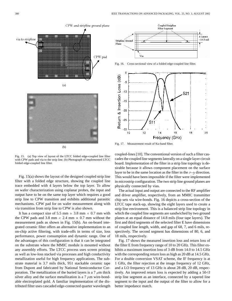
Fig. 17. Measurement result of Ku-band filter.
coupled-lines [10]. The conventional version of such a filter cas-cades the coupled line segments laterally on a single layer circuitboard. Implementation of the filter in a strip line topology is de-sirable because it allows component placement on the surfacelayer to be in the same location as the filter in the– direction.This would have been impossible if the filter were implementedin microstrip configuration. The two strip line ground planes arephysically connected by vias.
The actual input and output are connected to the RF amplifierand driver amplifier, respectively, from an MMIC transmitterchip sets via wire-bonds. Fig. 16 depicts a cross-section of theLTCC tape stack-up, showing the eight layers used to create astrip line environment. This is a balanced strip line topology inwhich the coupled line segments are sandwiched by two groundplanes at an equal distance of 14.8 mils (four tape layers). Thefirst and third segments of the selected filter E have dimensionsof coupled line length, width, and gap of 68, 7, and 6 mils, re-spectively. The second segment has dimensions of 80, 6, and18 mils, respectively.
Fig. 17 shows the measured insertion loss and return loss ofthe filter E from frequency range of 10 to 20 GHz. This filter ex-hibits a maximum insertion loss of 3 dB from 14.0 to 14.5 GHzwith the corresponding return loss as high as 20 dB at 14.5 GHz.For a double conversion VSAT scheme, the IF frequency is at1 GHz, the filter rejection at the image frequency of 12 GHz,and a LO frequency of 13 GHz is about 28 dB, 20 dB, respec-tively. An improved return loss is expected by adding a 50-strip line segment as an interface, connected by a tapered linesegment to the input and the output of the filter to allow for abetter impedance match.

LEE et al.: COMPACT LTCC-BASED KU-BAND TRANSMITTER MODULE 381
Fig. 18. Photograph of the implemented LTCC coupon and stripline filters.
Fig. 19. Exploded view of transmitter MCM module with LTCC integratedfilter.
V. LTCC-BASED MODULE DESIGN AND MEASURED
SYSTEM PERFORMANCE
A photograph of a implemented LTCC 951 coupon includingfour different completed transmitter modules and eight differenttest structures for coupled strip line BPF is shown in Fig. 18.The module occupies a compact area of 400310 35.2 mil .Fig. 19 depicts the three-dimensional exploded view of theLTCC module in which the MMIC chips were wire-bondedon the surface. The length of the wire-bond is approximately40 mil. The estimated loss of 40 mil ball crescent bond wiresincorporated in the module at 14 GHz is 2 dB [11]. The filterground planes were properly connected to the ground pads onthe surface layers and are wire-bonded to the ground pads onthe MMICs. The filter input was transitioned to the CPW lineand wire-bonded to the output of the RF amplifier while theoutput transition of the CPW was wire-bonded to the input ofthe driver amplifier. Such a configuration where the filter isintegrated between the mixer and the PA was chosen to elim-inate the mixer harmonics and the linearity of the transmitterwas improved. The transition to CPW also enables separate
Fig. 20. Double conversion transmitter block diagram with output spectrumat each block.
Fig. 21. Overall system gain performance with filter characteristics.
measurement of the filter. Fig. 20 shows the double conversiontransmitter block diagram and output spectrum at the outputof each block. The LO and image signal is attenuated afterthe BPF in the transmitter chain. Fig. 21 shows the measuredoverall system gain performance with filter characteristics.The entire transmitter chain exhibits a total conversion gain of41 dB and output power of 26 dBm incorporating the filter andwire-bond losses from 14 GHz to 14.5 GHz and LO rejection of20 dBc as well as image rejection of more than 40 dBc. Fig. 22shows the output spectrum of up-converter for a data rate of4 Mbps and 16 Mbps, respectively. The operability for Ku-bandapplication requires an output power of more than 24 dBm[12]. Spectrum mask for Ku-band system [12] requires relativepower spectrum levels of 9, 16, 26 dB at 0.3 , 0.35 ,0.5 frequency offsets from the center frequency, whereisdefined as the bit rate entering the modulator. Measurementresults of the chipset indicate that the output spectrum ofthe developed module fits well within the specified spectrummask for the data rates of 64, 128, 192, and up to 32 Mbpsas shown in Fig. 23, making it suitable for satellite outdoorunits. ACPR analysis has been performed to estimate thepower leakage between adjacent channels due to RF front-endnonlinearities. There are 6 channels within the 210 MHz bandas per direct broadcasting satellite (DBS) standard [12], hence

382 IEEE TRANSACTIONS ON ADVANCED PACKAGING, VOL. 25, NO. 3, AUGUST 2002
(a)
(b)
Fig. 22. Output power spectrum from up-converter with QPSK modulation(a) 4 Mbps QPSK modulation and (b) 16 Mbps QPSK modulation.
(a) (b)
(c) (d)
Fig. 23. Output power spectrum with the spectrum mask. (a) 64 Kbps, (b) 128Kbps, (c) 192 Kbps, and (d) 32 Mbps.
Fig. 24. ACPR with 32 Mbps data rate.
Fig. 25. Level diagram of the entire transmitter system with 1-dB compressionpoint.
TABLE IITRANSMITTER MODULE SYSTEM PERFORMANCE AT14 GHz, WITH A LO (13
GHz) POWER OF7 dBmAND AN IF (1 GHz) POWER OF�15 dBm
the adjacent channels are taken to be 41 MHz apart from eachother. Measured performance of chipset indicated an ACPR of42 dB for the transmitter module with a data rate of 32 Mbpsas shown in Fig. 24. Fig. 25 shows the measured system leveldiagram and 1-dB power compression performance of the

LEE et al.: COMPACT LTCC-BASED KU-BAND TRANSMITTER MODULE 383
entire transmitter chain based on the measurement of eachtransmitter blocks. Table II summarizes the overall systemperformance of transmitter module.
VI. CONCLUSION
This paper has presented the first demonstration of acompact LTCC-based transmitter module with functionalMMICs, which consist of VCO-mixer and PA implemented ina commercial GaAs MESFET technology. The up-converterMMIC demonstrated the conversion gain of 15 dB and IIP3of 15 dBm. The PA MMIC exhibits the total gain of 31 dBand 1-dB compressed output power of 26 dBm. The compactmodule was made possible by embedding the filter and therebyreducing the size of the area required by 40% compared tosuch a module implemented on a typical alumina substrate.The integrated strip line filter inserted between the mixer andthe PA demonstrates a low insertion loss of 3.0 dB from 14 to14.5 GHz. The transmitter module exhibits the total conversiongain of 41 dB and output power of 26 dBm incorporatingwire-bond and filter losses. Measured performance of thechipsets indicate that the output power spectral density atvarious data rates conforms to the spectral mask specification,thereby proving the applicability of the developed transmittermodule in the Ku-band satellite communication standard. Thisultra-compact module is an attractive solution for low-costKu-band satellite outdoor units. These approaches suggest thefeasibility of building highly SOP integrated microwave andmillimeter wave radio front-end development.
ACKNOWLEDGMENT
The authors would like to thank R. Brown and M. Ehlert, Na-tional Semiconductor, for fabricating the LTCC prototypes, aswell as the Staff of Triquint Semiconductor, for MMIC fabrica-tion.
REFERENCES
[1] J. V. Evans, “Proposed U.S. global satellite systems operating atKa-band,” inProc. IEEE Aerosp. Conf., vol. 4, 1998, pp. 525–537.
[2] W. Simon, R. Kulke, A. Wien, M. Rittweger, L. Wolff, A. Girard, andJ.-P. Bertinet, “Interconnects and transitions in multilayer LTCC multi-chip modules for 24 GHz ISM-band applications,” inProc. 2000 IEEEMTT-S Int. Dig., vol. 2, Boston, MA, pp. 1047–1050.
[3] K. Fujii, Y. Hara, Y. Shibuya, T. Sakai, and Y. Takano, “Highly integratedT/R module for active phased array antennas,” inProc. 1998 IEEE RFICDig., Baltimore, MD, pp. 77–80.
[4] J. W. Gipprich, L. E. Dickens, and J. A. Faulkner, “Power amplifieryields 10 W over 8–14 GHz using GaAs MMICs in an LTCC serialcombiner/divider network,” inProc. 1993 IEEE MTT-S Int. Dig., vol.3, Atlanta, GA, pp. 1369–1372.
[5] A. Sutono, J. Laskar, and W. R. Smith, “Development of three dimen-sional integrated bluetooth image reject filter,” inProc. IEEE MTT-S Int.Dig., vol. 1, Boston, MA, June 2000, pp. 339–342.
[6] J. A. Lester, M. Ahmadi, S. Peratoner, J. Hathaway, D. Garske, and P.D. Chow, “Low cost miniaturized EHF SATCOM transceiver featuringHEMT MMICs and LTCC multilayer packaging,” inProc. IEEE Mi-crow. Millimeter-Wave Monolithic Circuits Symp. Dig., 1995, pp. 35–38.
[7] C.-H. Lee, S. Han, B. Matinpour, and J. Laskar, “A low phase noiseX-band MMIC GaAs MESFET VCO,”IEEE Microwave Guided WaveLett., vol. 10, pp. 325–327, Aug. 2000.
[8] EM Users Manual. Liverpool, NY: Sonnet Software Inc.
[9] M. T. Jones and J. T. Bolljahn, “Coupled strip transmission line filtersand resonators,”IRE Trans. Microwave Theory Tech., vol. MTT-4, pp.75–81, Apr. 1956.
[10] S. B. Cohn, “Parallel coupled transmission-line-resonator filters,”IRETrans. Microwave Theory Tech., vol. MTT-6, pp. 223–231, Apr. 1958.
[11] A. Sutono, N. G. Cafaro, J. Laskar, and E. M. Tentzeris, “Experimentalstudy and modeling of bond wire interconnects for microwave integratedcircuits,” inProc. IEEE AP-S Conf., vol. 4, Salt Lake City, UT, Jan. 2000,pp. 2020–2023.
[12] INTELSAT Earth Station Standards (IESS) Document IESS-208, Tech.Rep., 2002.
Chang-Ho Lee (M’01) received the B.S. and M.S.degree in electrical engineering from Korea Univer-sity, Seoul, Korea, in 1989 and 1991, respectively,and the M.S. and Ph.D. degrees in electrical andcomputer engineering from Georgia Institute ofTechnology, Atlanta, in 1999 and 2001, respectively.
He was a Research Engineer with DACOM Cor-porations, Korea, for three years. In 2000, he joinedRF Solutions, Inc., Norcross, GA, where he is a StaffEngineer. His research interest includes satellite com-munication system simulation, design, and character-
ization of the transceiver MMICs in GaAs MESFET, pHEMT, and HBT pro-cesses, as well as LTCC-based multilayer multichip modules development forsatellite and wireless communication applications. His current research is re-lated to dual-band transceiver design for WLAN applications.
Albert Sutono received the Ph.D. degree in elec-trical engineering from the Georgia Institute ofTechnology, Atlanta, in 2001.
He has one U.S. patent pending and au-thored/co-authored over 40 peer-reviewed IEEE andinternational journal and conference publications inthe area of ceramic and organic-based microwaveand millimeter wave integrated modules, in additionto several invited talks. He held a position as aM(M)IC Design Engineer at RF Solutions, Norcross,GA, before joining Infinera, Inc., Sunnyvale, CA, in
2002. His current research is millimeter wave-photonic device modeling andcharacterization.
Sangwoo Han received the B.S. degree fromCarnegie-Mellon University, Pittsburgh, PA, in1992, the M.S. degree from the University of Penn-sylvania, Philadelphia, in 1993, and the Ph.D. degreefrom the Georgia Institute of Technology, Atlanta,in 2000. His doctoral work includes development ofMMIC-based mult-chip and single-chip transmittermodules for an optical sub-carrier multiplexing(OSCM) communication link.
He was responsible for the complete design andcharacterization of all MMIC chipsets, filters, and
boards for these modules. In 1998, he joined RF Solutions, Inc., Norcross,GA, where he has developed GaAs MESFET 3.5 GHz and UNII band poweramplifiers for fixed wireless applications and GaAs HBT UNII band poweramplifiers for wireless LAN applications. He has also developed a model forimplementation of a W-CDMA RF sub-system focusing on optimization ofsystem performance and cost. He has over seven years of experience in RFsub-system and MMIC designs. Prior to RF Solutions, he worked in the areasof RF sub-system simulations and RF transceiver designs at Electronics andTelecommunications Research Institute (ETRI), Korea, and Hewlett-Packard(HP). He has written and contributed to several Microwave Theory andTechniques (MTT) Journal publications and presented at many conferences onRF/optical communications and RF transceiver design.

384 IEEE TRANSACTIONS ON ADVANCED PACKAGING, VOL. 25, NO. 3, AUGUST 2002
Kyutae Lim (M’99) was born in Seoul, Korea, in1968. He received the B.S., M.S., and Ph.D. degreesfrom Hanyang University, Seoul, Korea, in 1991,1993, and 1996, respectively.
From 1996 to 2000, he was with the SamsungAdvance Institute of Technology, Kiheung, Korea,as a Technical Staff, Member where he was involvedin developing mm-wave wireless LAN systems.From 1998 to 1999, he was with the CommunicationResearch Laboratory, Tokyo, Japan, as a ResearchFellow, where he developed planar antennas and
packages for 60 GHz. In January 2000, he joined the Microwave ApplicationGroup, Georgia Institute of Technology, Atlanta, as a Research Engineer.He has authored and co-authored over 40 papers and holds two patents. Hisresearch interests include the development of the passive/active circuits forRF/wireless and high-speed opto-electronic applications. He also interested inthe mixed signal system integration by the system-on-packaging concept.
Dr. Lim is a member of IEEE Microwave Theory, Component, Packaging,and Manufacturing Technology, and Technique and Antennas and PropagationSocieties.
Stéphane Pinelwas born in Toulouse, France, in1974. He received the B.S. degree from Paul SabatierUniversity, Toulouse, France, in 1997 and the Ph.D.degree in microelectronics and microsystemsfrom the Laboratoire d’Analyze et d’Architecturedes Systemes, Centre National de la RechercheScientifique, Toulouse, in 2000.
He has worked on a ultrathin chip stacking (UTCS)European Project for three year and is currently doingPost-Doctoral work at the Microwaves ApplicationsGroup, Georgia Institute of Technology, Atlanta. His
research interests include advanced 3-D integration and packaging technologies,RF packaging and RF-MEMS, system-on-package for RF front-end module,and SOI RF circuit design.
Emmanouil M. Tentzeris (M’99) received theDiploma degree in electrical engineering andcomputer science (with high honors) from theNational Technical University, Athens, Greece, in1992 and the M.S. and Ph.D. degrees in electricalengineering and computer science from the Uni-versity of Michigan, Ann Arbor, in 1993 and 1998,respectively.
He joined the School of Electrical and ComputerEngineering, Georgia Institute of Technology(Georgia Tech), Atlanta, in 1998 as an Assistant
Professor, and he is currently the leader of the Novel Integration TechniquesSubthrust, Broadband Hardware Access Thrust, Yamacraw Initiative, State ofGeorgia, and the Packaging Research Center Thrust Leader for RF/WirelessPackaging. At Georgia Tech, he has established academic programs innumerical electromagnetics, RF/wireless applications, packaging adaptiveultracompact antennas, and RF MEMS modeling: over 75 publications, threebook chapters, and numerous invited papers.
Dr. Tentzeris received the National Science Foundation CAREER Award(2000), the Georgia Tech-ECE Outstanding Junior Faculty Award (2002),the International Hybrid Microelectronics and Packaging Society Best PaperAward (1997), and the Applied Computational Electromagnetics SocietyBest Paper Award (2001). He has been an Invited Professor at the TechnicalUniversity of Muenchen, Munich, Germany, Summer 2002. He was the1999 Technical Program Co-Chair of the 54th ARFTG Conference and heis currently a member of the Technical Program Committees of IEEE-IMSand IEEE-AP Symposiums. He is the Vice-Chair of IEEE-CPMT TC16 (RFSubcommittee).
Joy Laskar (M’91) received the B.S. degree (withhighest honors) in computer engineering fromClemson University, Clemson, SC, in 1985 and theM.S. and Ph.D. degrees in electrical engineeringfrom the University of Illinois, Urbana-Champaign,in 1989 and 1991, respectively.
Prior to joining the Georgia Institute of Tech-nology (Georgia Tech), Atlanta, in 1995, he heldfaculty positions at the University of Illinois andthe University of Hawaii. At Georgia Tech, he iscurrently the Chair for the Electronic Design and
Applications Technical Interest Group, the Director of Research for the stateof Georgia’s Yamacraw Initiative, and the NSF Packaging Research CenterSystem Research Leader for RF and Wireless. His research has focused onhigh frequency IC design and their integration. At Georgia Tech, he heads aresearch group of 25 members with a focus on integration of high frequencyelectronics with optoelectronics and integration of mixed technologies for nextgeneration wireless and optoelectronic systems. His research is supported byover 15 companies and numerous federal agencies including: DARPA, NASAand NSF. He has published over 100 papers, numerous invited talks and has10 patents pending.
Dr. Laskar received the Army Research Office’s Young Investigator Awardin 1995, the National Science Foundation’s CAREER Award in 1996, the NSFPackaging Research Center Faculty of the Year in 1997, the NSF Packaging Re-search Center Educator of the Year in 1998, the IEEE Rappaport Award (BestIEEE Electron Devices Society Journal Paper) in 1999, and the IEEE MTT IMSBest Paper award in 2000. He is a co-Organizer and Chair for the Advanced Het-erostructure Workshop, serves on the IEEE Microwave Theory and TechniquesSymposia Technical Program Committee, and is a member of the North Amer-ican Manufacturing Initiative Roadmapping Committee, and is co-founder of aBroadband Wireless Company, RF Solutions.