3d ics: recent advances in the industry€¦ · -slow imc reaction -large vol shrinkage hybridized...
TRANSCRIPT

© Copyright 2014 Xilinx .
3D ICs: Recent Advances in the Industry Suresh Ramalingam Senior Director, Advanced Packaging

© Copyright 2014 Xilinx .
• 3D IC Background
• 3D IC Technology Development
• Summary
•Acknowledgements
Outline
Stacked Silicon Interconnect Technology Refers to Xilinx 3D solutions
© Copyright 2014 Xilinx .
3D IC Background

© Copyright 2014 Xilinx .
Technical Challenges & Costs Are Growing
Process Technology Path Below 7nm is unclear
Cost Reduction Slowing from Complexity / Investment Increases
Cost Per Wafer & Cost Per Gate Deviating from Historical Reduction

© Copyright 2014 Xilinx .
Technical Challenges & Costs Are Growing
Process Technology Path Below 7nm is unclear
Cost Reduction Slowing from Complexity / Investment Increases
Cost Per Wafer & Cost Per Gate Deviating from Historical Reduction

© Copyright 2014 Xilinx .
3DIC Extends Moore’s Law Cost Comparison: Monolithic vs. Multi-Die
Die Area
Die
Co
st Monolithic
Multi-Die
“Moore’s Law is Really About Economics” – Gordon Moore
© Copyright 2014 Xilinx .
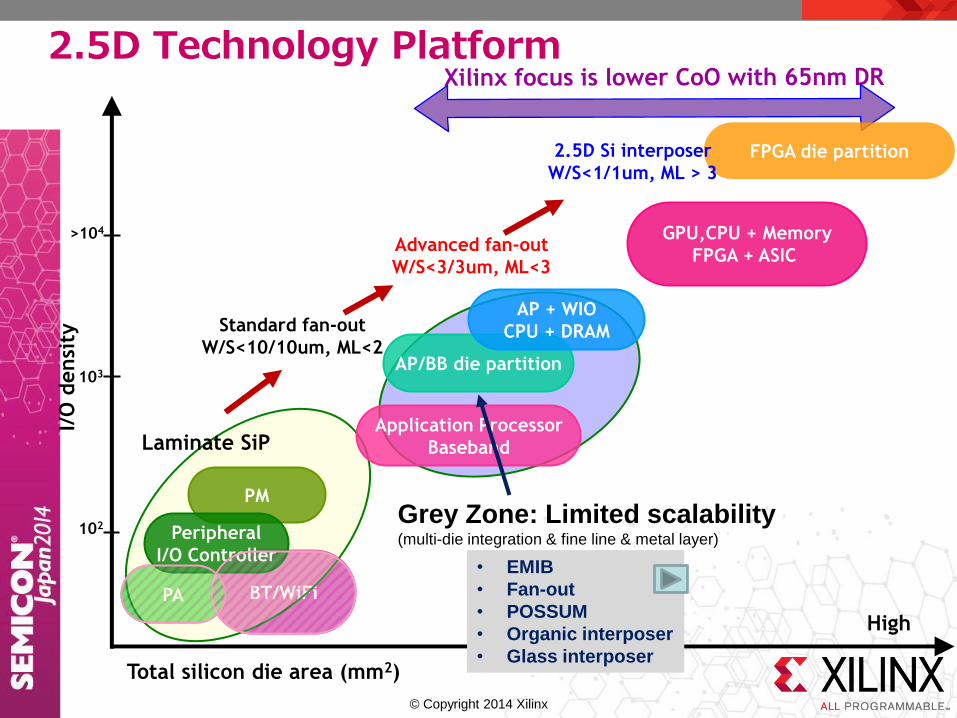
2.5D Technology Platform
Total silicon die area (mm2)
BT/WiFi PA
PM
Peripheral
I/O Controller
Laminate SiP
High
I/O
densi
ty
102
103
>104
Application Processor
Baseband
AP/BB die partition
AP + WIO
CPU + DRAM Standard fan-out
W/S<10/10um, ML<2
Advanced fan-out
W/S<3/3um, ML<3
GPU,CPU + Memory
FPGA + ASIC
FPGA die partition 2.5D Si interposer
W/S<1/1um, ML > 3
• EMIB
• Fan-out
• POSSUM
• Organic interposer
• Glass interposer
Grey Zone: Limited scalability (multi-die integration & fine line & metal layer)
© Copyright 2014 Xilinx .
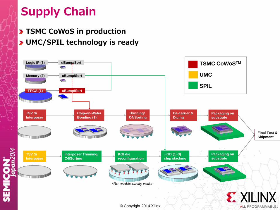
Supply Chain
TSMC CoWoS in production
UMC/SPIL technology is ready
TSV Si
Interposer
TSV Si
Interposer
Chip-on-Wafer
Bonding (1)
FPGA (1)
Memory (2)
Logic IP (3)
Thinning/
C4/Sorting
Packaging on
substrate
Final Test &
Shipment
TSMC CoWoSTM
UMC
SPIL
Interposer Thinning/
C4/Sorting
KGI die
reconfiguration
*Re-usable cavity wafer
De-carrier &
Dicing
Packaging on
substrate
uBump/Sort
uBump/Sort
uBump/Sort
KGD (1~3)
chip stacking

© Copyright 2014 Xilinx .
Virtex-7 2000T
Interposer Area: ~775 mm2
Population: ~6.8 Billion Transistors
Chips: 5
Earth
Area: ~500 Million km2
Population: ~6.8 Billion People
Oceans: 5
Xilinx 28nm 3D IC – Huge Leap in Innovation
136 Patents Awarded Worldwide
226 Pending Applications Worldwide

© Copyright 2014 Xilinx .
3D IC Technology Development

© Copyright 2014 Xilinx .
3D IC Anatomy & Assembly Flow
Micro-Bumps Power / Ground / IOs / Routing
Through-Silicon Via (TSVs) Connects Power / Ground / IOs to C4 Bumps
Passive Silicon Interposer (65nm) 4 Metal Layers Connecting Micro-Bumps & TSVs
C4 Bumps Connects Silicon to Package
> 150,000 Micro-bumps
> 10,000 TSVs
> 10,000 C4 Bumps
> 90 Processing Steps in 3D IC Flow
(From Bump to Completed Package)
Primary Chip on Wafer Assembly Steps
Achieved Good Yield & Quality

© Copyright 2014 Xilinx .
CoWoS Technology
– Top dies are attached to full-thickness interposer wafers thus getting around the thin
interposer warpage and poor micro-bump joining problem
Reconfigurable CoW (rCoW) Technology
– Xilinx patent issued worldwide (US/TWN/CN/EU/IND/JPN/KR)
– Release layer approach that withstands reflow & maintains low warpage
Warpage control Keep warpage below <10um over entire temp range
CoS
CoWoS rCoW
Critical Challenge: Warpage Control

© Copyright 2014 Xilinx .
HTS Aging Reliability Issue
Voiding or crack in micro-joint during long term stress (HTS in particular)
– Due to limited Sn source and its dual consumption rate from top and bottom pad
Resolution : Heavy Cu doping into LF solder cap (with Ni barrier layer)
– Take advantages of ductile IMC (Cu-Sn) and slower IMC reaction (Ni with Cu-Sn IMC)
– Passed 3X reflow + 150oC aging condition for > 1000 hrs
-Stable Cu-Sn IMC
-Super slow IMC reaction
Standard
Cu/Solder
Diffusion flux model of inter-diffusion HTS aging performance
-Fast Cu-Sn reaction
-kirkendal void form
-Ductile IMC
-Brittle NiSn IMC
-Slow IMC reaction
-Large Vol shrinkage
Hybridized
*Reference images
(from no-doping u-bump)

© Copyright 2014 Xilinx .
Leadership Continues at 20/16nm - UltraSCALE
4.4M Logic Cells in 20nm
14B transistors
600,000 micro-bumps
55mm package, 2892 pins

© Copyright 2014 Xilinx .
Leadership Continues at 20/16nm - UltraSCALE
32G TX Eye
2.0 dB insertion loss at Nyquist
Frequency
Low loss substrate and design
23,000 C4 bumps
© Copyright 2014 Xilinx .
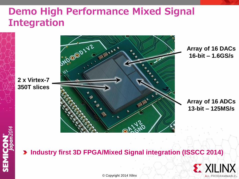
Demo High Performance Mixed Signal Integration
2 x Virtex-7
350T slices
Array of 16 DACs
16-bit – 1.6GS/s
Array of 16 ADCs
13-bit – 125MS/s
Industry first 3D FPGA/Mixed Signal integration (ISSCC 2014)

© Copyright 2014 Xilinx .
Si-Less/TSV-less Interconnect Tech (SLIT) Builds on Interposer Platform
Key Benefits
Lower cost of ownership
- No HR-Si substrate used & less process
modules (No TSV module/TBDB/TSV
revealing)
SLIT (Under development)
Structure
High-R Si substrate
65nm 4X Metal
TSV Creation
Micro-bumping
Temporary carrier
Thinning
TSV Revealing
Xilinx, SPIL (iMAPS 2014)
© Copyright 2014 Xilinx .
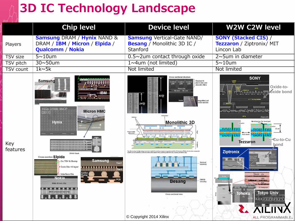
3D IC Technology Landscape
Oxide-to-
oxide bond
Cu-to-Cu
bond
Chip level Device level W2W C2W level
Players
Samsung DRAM / Hynix NAND & DRAM / IBM / Micron / Elpida / Qualcomm / Nokia
Samsung Vertical-Gate NAND/ Besang / Monolithic 3D IC / Stanford
SONY (Stacked CIS) / Tezzaron / Ziptronix/ MIT Lincon Lab
TSV size 5~10um 0.5~2um contact through oxide 2~5um in diameter
TSV pitch 30~50um 1~4um (not limited) 5~10um
TSV count 1k~5k Not limited Not limited
Key features

© Copyright 2014 Xilinx .
Economic and technology forces
are aligned to enable 2.5D/3D
stacking
The “end game” will see three distinct
technologies: Logic, Memory, Analog
TSV and 3D stacking already deployed
in Smartphones, High end FPGAs &
Servers
Summary
Analog Logic
Mem
Package
© Copyright 2014 Xilinx .
•Xilinx – R&D, Reliability, NPI, Operations and Marketing Teams
•Partners – TSMC R&D and Production Teams for FPGA, CoWoS
– UMC for Interposer
– SPIL R&D for MEOL and Advanced Packaging
– Fujitsu Interconnect Technology for High Speed Substrates
Acknowledgements

© Copyright 2014 Xilinx .
Design Rule Comparison
Design Rules for Die to Die interconnection
MCM (Substrate)
EMIB Silicon Interposer (65 nm BEOL)
WLFO / Organic Interposer
Minimum Bump pitch (um) 150 (C4) 150 (C4) 40 (u-bump) bridge
< 40 (u-bump) 40 um RDL pad pitch
Via size / pad size (um) 60 / 90 0.4 / 0.7 0.4 / 0.7 10/30
Minimum Line & Space (um) 15 / 15 0.4 / 0.4 0.4 / 0.4 3 / 3
Metal thickness (um) 10 1 1 2-5
Dielectric thickness (um) 30 1 1 < 5
# of die-to-die connections per layer + GND shield layer (2L)
100’s 10,000’s 10,000’s 1000’s
Minimum die to die spacing (um)
4000 Bridge ~ 2500 150 < 250
# of High density layers feasible
Not a limitation Not a limitation Not a limitation 1-3L layers
Die Sizes for assembly and # of assemblies
Not a concern Size & # limitation?
Not a concern Size limitation?
Xilinx pursuing Silicon Interposer for design rule
density, BW and lower power – e.g. die partition