4.5.4 pulse code modulationresource.download.wjec.co.uk.s3.amazonaws.com/vtc/2013-14... · topic...
TRANSCRIPT

Topic 4.5.4 – Pulse Code Modulation
1
Learning Objectives: At the end of this topic you will be able to;
analyse and draw graphs to illustrate pulse amplitude modulation (PAM) techniques (covered in topic 4.3.5 Pulse modulation);
relate required sampling frequency to the highest frequency in the signal;
draw a block diagram for, and describe the operation of, a PCM communication system consisting of; o transmitter
low pass filter sampling gate sampling clock ADC PISO shift register PISO clock
o receiver Schmitt trigger SIPO shift register SIPO clock DAC low pass filter
relate resolution to the number of sampling levels, and select and use the formula:
n
range voltage inputresolution
2 .
describe how time division multiplexing (TDM) can be used to improve the capacity of a PCM communications link, using TDM.
Module ET4 – Communication Systems
2
Pulse Code Modulation
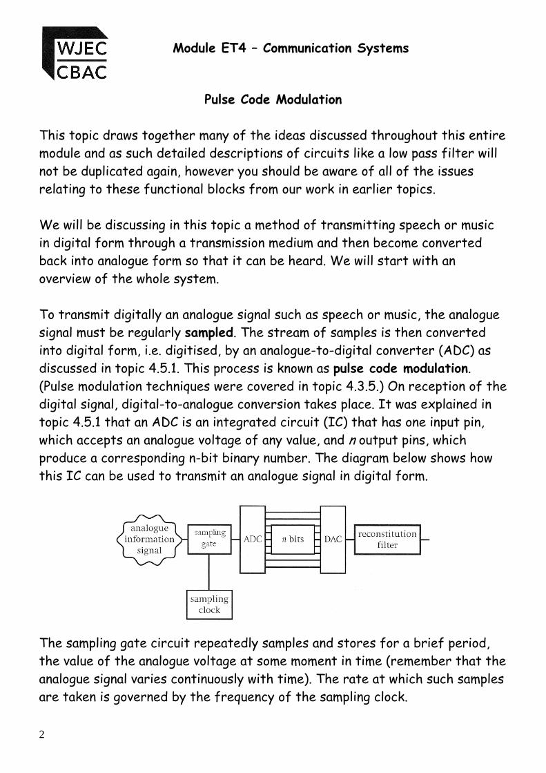
This topic draws together many of the ideas discussed throughout this entire module and as such detailed descriptions of circuits like a low pass filter will not be duplicated again, however you should be aware of all of the issues relating to these functional blocks from our work in earlier topics. We will be discussing in this topic a method of transmitting speech or music in digital form through a transmission medium and then become converted back into analogue form so that it can be heard. We will start with an overview of the whole system. To transmit digitally an analogue signal such as speech or music, the analogue signal must be regularly sampled. The stream of samples is then converted into digital form, i.e. digitised, by an analogue-to-digital converter (ADC) as discussed in topic 4.5.1. This process is known as pulse code modulation. (Pulse modulation techniques were covered in topic 4.3.5.) On reception of the digital signal, digital-to-analogue conversion takes place. It was explained in topic 4.5.1 that an ADC is an integrated circuit (IC) that has one input pin, which accepts an analogue voltage of any value, and n output pins, which produce a corresponding n-bit binary number. The diagram below shows how this IC can be used to transmit an analogue signal in digital form.
The sampling gate circuit repeatedly samples and stores for a brief period, the value of the analogue voltage at some moment in time (remember that the analogue signal varies continuously with time). The rate at which such samples are taken is governed by the frequency of the sampling clock.

Topic 4.5.4 – Pulse Code Modulation
3
The ADC converts each sample of the analogue information into a code of n bits. These n-bit codes are transmitted in parallel along n wires, one sample after another, to a matching n-bit digital-to-analogue converter (DAC). This produces a stepped analogue voltage from the incoming codes. The output is often referred to as a staircase approximation to the original analogue signal.
The reconstitution filter is essentially a filter circuit that smoothes out the quantisation steps from the DAC. It operates in such a way that it appears to change the staircase waveform into a smooth curve.
2-bit DAC Output
3-bit DAC Output

Module ET4 – Communication Systems
4
Now we will take a look in more detail at the individual parts of the system to determine their critical importance to the system. We will start at the very beginning with the first process, which is the sampling of the analogue waveform. The ability of this system to transmit and more importantly recover the original analogue information is dependent on the sampling rate (sampling frequency) relative to the information frequency. To illustrate this effect, consider the series of diagrams below. Diagram (a) shows a sinusoidal information signal (i.e. a pure tone) of frequency 500 Hz;
Diagram (b) shows the result of sampling every 2.5 ms (i.e. the sampling frequency is 400 Hz); Diagram (c) shows the reconstituted output.

Topic 4.5.4 – Pulse Code Modulation
5
It can be seen that the recovered information signal is not at all like the original. Indeed, the original signal has been lost and a lower-frequency signal has replaced it. This lower-frequency signal is called an alias and has appeared because the sampling frequency is far too low. Great care must be taken to avoid aliasing when converting analogue signals into digital. In 1924, the Dutch mathematician Harry Nyquist first showed that to recover an information signal from a series of samples, the sampling frequency must be greater than twice the maximum frequency fmax in the information. This is known as the sampling theorem and the frequency 2xfmax
is known as the Nyquist frequency. The diagram below shows the same 500 Hz information signal but this time sampled at a frequency of 2 kHz (i.e. greater than the Nyquist frequency, which is 2 x 500 Hz).
The recovered output can clearly be seen to be a rough copy of the original.

Module ET4 – Communication Systems
6
The sampling clock frequency must therefore be greater than 2 x fmax of the signal to be sampled. To prevent issues with aliasing occurring with the digitisation of an analogue signal when the analogue signal has a range of frequencies, it is absolutely essential to pass the analogue signal through a low pass filter (topic 4.2.3 Passive RC filters) before sampling. In this way, all the frequencies that are too high for the given sampling rate are removed, so that no aliases are generated. The system therefore becomes:
Anti-alias examples In the telephone system, voice frequencies are restricted to the range
300 Hz to 3.4 kHz. So the low pass filter is set up to pass only this range of frequencies to the sampling gate circuit. The sampling frequency is 8000 Hz, which satisfies the Nyquist criterion of being greater than twice 3.4 kHz, the maximum baseband frequency.
When making a compact disc, the recording studio passes the music
signal through a low pass filter that limits the maximum frequency to 20 kHz. Sampling is then taken at a frequency of 44.1 kHz, which again satisfies the Nyquist criterion of being greater than twice the 20 kHz maximum.

Topic 4.5.4 – Pulse Code Modulation
7
Student Exercise 1 1. An audio signal has a baseband that ranges from 0.5 kHz to 4.5 kHz. If
this signal is to be digitised, state which of the following frequencies would be a suitable sampling frequency:
A: 4.0 kHz, B: 5.0 kHz, C: 6.8 kHz, D: 8.2 kHz, E: 9.8 kHz, F: 18 kHz Answer(s): …………………………………………………. Now that we have established the criteria for making the sampling gate operate at an appropriate frequency, we will turn our attention to the ADC and the conversion process in general. The construction of the ADC circuit will be covered in module ET5, so we do not need to worry about that here. However there are a few things we need to consider about its operation. Firstly we need to think about what the ADC is actually doing, that is changing an analogue voltage into a series of digital pulses. The accuracy with which this can be achieved will depend on how many bits are available for the digital coding. Let us look at some examples to illustrate this. In a two bit system only 4 possible digital codes, 00, 01, 10, 11 are possible. Each one of these would be allocated to a voltage level in the original signal. For example with an input voltage range of 0-16V, only 4 digital codes are available so the input voltage range can only be split into 4 different levels, in this case with each being equal to 16/4 = 4V.

Module ET4 – Communication Systems
8
So an input voltage between 0 and 4V would be coded as 00, between 4.001V and 8V would be coded as 01, between 8.001V and 12V would be coded as 10, between 12.001V and 16V would be coded as 11.
At the receiver the reverse process takes place where digital codes are converted into analogue voltage values using a device called a summing amplifier which again will be discussed in detail in Module ET5. At the receiver the codes would be interpreted as follows:
An input of 00 produces an output of 0V An input of 01 produces an output of 4V An input of 10 produces an output of 8V An input of 11 produces an output of 12V
This is easier to see graphically as shown below:
V1 is the analogue input voltage range and V2 would be the output from a corresponding 2 bit DAC. Even early observations show that the output is nothing like the original, the voltage is always lower than the original and the steps are far too large to make this suitable for any form of communication system. How does the system improve if we use three bits?
2-bit ADC Output

Topic 4.5.4 – Pulse Code Modulation
9
In a three bit system an extra 4 digital codes are available making 8 in total, 000, 001, 010, 011, 100, 101, 110, 111 are possible. Each one of these would be allocated to a voltage level in the original signal. For example with an input voltage range of 0-16V, and 8 digital codes are available so the input voltage range can only be split into 8 different levels, in this case with each being equal to 16/8 = 2V. So an input voltage
between 0 and 2V would be coded as 000, between 2.001V and 4V would be coded as 001, between 4.001V and 6V would be coded as 010, between 6.001V and 8V would be coded as 011, between 8.001V and 10V would be coded as 100, between 10.001V and 12V would be coded as 101, between 12.001V and 14V would be coded as 110, between 14.001V and 16V would be coded as 111.
At the receiver the codes would be interpreted as follows:
An input of 000 produces an output of 0V An input of 001 produces an output of 2V An input of 010 produces an output of 4V An input of 011 produces an output of 6V An input of 100 produces an output of 8V An input of 101 produces an output of 10V An input of 110 produces an output of 12V An input of 111 produces an output of 14V
This is easier to see graphically as shown below:
3-bit ADC Output

Module ET4 – Communication Systems
10
V1 is the analogue input voltage range and V2 would be the output from a corresponding 3 bit DAC. Whilst this is better than the 2-bit example it still does not come close to reproducing the original signal. It should now be obvious that if we are to get anywhere close to the original signal at the receiver the number of bits required will have to be increased dramatically so that the step size at the receiver is reduced as much as possible. In practice a minimum of 8 bits is required to allow a good reproduction of the original signal. For an 8-bit digital code there will be 28 possible combinations, i.e. 256. This means that the step size would now be 16/256=0.0625V or 62.5mV. You should be able to see now that even with just 8 bits, the size of the step is becoming very small, and therefore we will be getting very close to the original signal value. In general we can quote the resolution of an ADC using the following formula:
n
range voltage inputresolution
2
Where ‘n’ is the number of bits. Student Exercise 2 A CD-Player uses a 16-bit encoding system. If the maximum voltage range is 5V, calculate the resolution of the CD System. ……………………………………………………………………………………………………………………………………………
……………………………………………………………………………………………………………………………………………
……………………………………………………………………………………………………………………………………………
……………………………………………………………………………………………………………………………………………

Topic 4.5.4 – Pulse Code Modulation
11
Parallel to Serial In the system shown on Page 6, parallel transmission of the information takes place between the transmitter and the receiver. This means that the n bits of code are simultaneously sent down n separate wires at a rate governed by the frequency of the sampling clock. Although this is the fastest (and simplest) method by which a digital signal can be transferred, it is not viable when the transmission distance is more than a few metres. There are two reasons for this.
The cost of a long cable composed of n wires would be high. When transmitting in parallel each bit of an n-bit word could take a
slightly different time to travel along its individual pair of wires. As the cable becomes longer and longer the effect worsens, and the n bits may not be received at the exact same moment in time. This may result in incorrect data being received.
Consequently, the parallel transmission of digital data is only used where fast data transfer is required over short distances, for example in the link between a computer and a printer. The alternative is to use a single conductor for the data transfer. The diagram above shows how a single link can be used to transfer the information, and you should recognise another two of the functional blocks in this diagram from our previous work.
PISO Clock
SIPO Clock
Parallel to Serial Shift
Register PISO
Serial to Parallel Shift Register SIPO
Transmission medium

Module ET4 – Communication Systems
12
The diagram shows the basic arrangement for transmitting the n bits of code along a single link. These n bits of code from the ADC are input to a parallel-to-serial shift register. As we found out in topic 4.5.3 this circuit loads the entire n-bit word on one clocking pulse and then transmits it, one bit at a time (under the control of another clocking pulse). These n bits progress along the single link to the receiver and it is in this single link that the digital signal exists. If a serially transmitted digital signal is examined on an oscilloscope then it is observed to be an apparently random procession of 1s and 0s, as shown below.
The full block diagram of the transmitter is shown below.

Topic 4.5.4 – Pulse Code Modulation
13
The full block diagram of the receiver is shown below.
The receiver contains a serial-to-parallel shift register. This circuit takes in the bits as they arrive, one after the other, and temporarily stores them. Once it has received all n bits, it outputs the entire n-bit word in parallel to a DAC (to recover the original analogue signal). In practice the signal arriving from the end of the communication link will be attenuated and more than likely to suffer from the effects of noise. It will pass through a Schmitt trigger (topic 4.5.2) in order to regenerate the signal before it is passed to the SIPO shift register. In a PCM system, the parallel-to-serial and serial-to-parallel circuits have to work fast, because they must input, and shift the n bits of each sample before the next n-bit sample arrives for transmission. That is to say, the PISO clock for the parallel-to-serial and SIPO clock for the serial-to-parallel circuits have to run at a much faster rate than the original sampling clock. For example: If the original sampling clock is running at 2kHz, i.e. with a period of 0.5ms, and the ADC is a 12-bit device, then the 12 bits have to be loaded into the PISO and output before the next sample arrives. Therefore the maximum time permissible per bit is 0.5ms/12=41.6µs. This gives a minimum PISO frequency of 24kHz. To allow some tolerance a frequency of 30kHz could be used.
From Communications Link

Module ET4 – Communication Systems
14
Before we look at some examination style questions on this topic there is just one more issue to deal with, and that is related to maximising the use of the serial communications link. The most common use of PCM is in the telecommunications business and being able to maximise the use of a serial link between two places is of paramount importance. This is best illustrated by considering an example. A telephone conversation is limited to a frequency range of 3.4kHz. For a successful conversion to take place the Nyquist sampling theorem states that the sampling rate must be at least double the highest frequency, i.e. 2 x 3.4 = 6.8kHz. To make the numbers a bit easier we will sample at a frequency of 8kHz. In time terms this means a sample is taken every 1/8000=125µs. If the ADC is a 12-bit device, the PISO will have to output these 12 bits before the end of the 125µs period otherwise the next sample will be taken by the sampling gate and overwrite some of the data still stored in the PISO before it has completed the output sequence. If we assume that the PISO clock has a period of 10µs, then 12 bits will take 12 x 10µs = 120µs to output. This can be seen on the graph below. The upper frequency limit of the PISO clock is independent of the sampling clock frequency and modern electronic circuitry is able to operate as very high frequencies. Consider what would happen if the PISO clock was running at 1MHz, i.e. each cycle would last 1µs. To output 12 bits would just require 12µs.
Transmit 12 bits Transmit 12 bits
0 125 250 time (µs)
Sampling Pulse
0 125 250 time (µs)

Topic 4.5.4 – Pulse Code Modulation
15
This would change our previous graph to the one shown below.
We can now see that we have created a large time gap in the communication link between samples where the line is now effectively idle. This would be very expensive, and a waste of resource so during this period where the current conversation sample is not being transmitted, another sample from a different conversation is fed into the communication link as shown below.
0 125 250 time (µs)
Transmission of data
Sampling Pulse
0 125 250 time (µs)
0 125 250 time (µs)
Data from conversation 1
Data from conversation 2
Sampling Pulse
0 125 250 time (µs)

Module ET4 – Communication Systems
16
There are still opportunities to fit other conversations into the gaps that still remain before having to return to pick up the next sample from the original conversation as shown below. Here we can see that 5 conversations fit easily into the space between sampling of the original conversation. This technique makes maximum use of the communications link, and is called time division multiplexing. Each conversation shares the communications link for a short period, which makes maximum use of the link. A multiplexer selects the conversations in turn and feeds them into the communications link. At the end of the link a demultiplexer passes the information back to the appropriate receiver. The diagram below should help you to visualise this.
1 1
0 125 250 time (µs)
12 2 2 3 34 45 5
Sampling Pulse
0 125 250 time (µs)
Channel 1
Channel 2
Channel 3
Channel 4
Channel 5
Channel 1
Channel 2
Channel 3
Channel 4
Channel 5
Transmission Link
Multiplexer De-Multiplexer
Low Pass Filter
Low Pass Filter
Low Pass Filter
Low Pass Filter
Low Pass Filter
Audio Signal
Low Pass Filter
Low Pass Filter
Low Pass Filter
Low Pass Filter
Low Pass Filter
Audio Signal
Encoder
Decoder
Transmit Section Receive Section

Topic 4.5.4 – Pulse Code Modulation
17
The PCM transmitter and receiver have a slightly different design to the ones shown for a non multiplexed link. Each channel has individual low pass filters, but to make the system more cost effective the rest of the transmitter circuitry is shared by all channels. The multiplexer acts as a sampling gate to produce PAM signals of each channel in turn. The ADC in the encoder then produces blocks of binary digits for each sample in turn which are converted into a serial bit stream by the PISO. The Schmitt trigger in the decoder regenerates the binary bit stream before the SIPO produces blocks of binary digits which are reconstructed into a PAM signal of each channel in turn. The demultiplexer routes each reconstructed PAM signal to the correct channel The multiplexer and de-multiplexer are synchronised using additional channels on the system to ensure that caller on transmit channel 1 is connected to receive channel 1 so that the correct samples of each conversation
You will need to know how to calculate how many signals can be transmitted using this technique given the relative information for a given system. This is achieved by dividing the period between samples by the time needed to transmit the individual bits from the PISO. In general
period PISO bits of No
period sampling channels of Number
For the above example the number of channels that can be transmitted is
channels .s
s
period PISO bits of No
period sampling channels of Number
104110112
125
Module ET4 – Communication Systems
18
The above system would have to be duplicated to enable a two way conversation to be held, using a second transmission link. In a real system BT transmit 30 speech channels over two transmission links therefore saving 28 communication links.
Now complete Student Exercise 3.

Topic 4.5.4 – Pulse Code Modulation
19
Student Exercise 3. 1. (a) Complete the diagram for the receiver for a Pulse Code Modulation
(PCM) communication system.
[1]
(b) The digital-to-analogue converter has a 12-bit input and output voltage range of 0V to 8V. What is the resolution of the DAC?
..............................................................................................................................
..............................................................................................................................
..............................................................................................................................
[2] (c) The low pass filter cuts off frequencies above 10kHz. Why is this
needed in this system? ..............................................................................................................................
..............................................................................................................................
..............................................................................................................................
..............................................................................................................................
..............................................................................................................................
[1]
Module ET4 – Communication Systems
20
2. Time Division Multiplexing (TDM) can be used to transmit several Pulse Code Modulation (PCM) channels along a single communications link.
Read the passage below and use the information given to answer the
questions which follow. The system uses a PCM sampling gate frequency of 25 kHz to convert
audio signals in the range 20 Hz - 10 kHz into digital form. A 10-bit code is used to define the sample levels with an input voltage range of 0 to 5V. Several signals are sent along one carrier using TDM. The PISO clock rate of each PCM channel is 2 MHz. A number of PCM channels are transmitted down a single TDM link.
(a) Why is a PCM sampling frequency of 25kHz suitable in this
application? ..............................................................................................................................
.............................................................................................................................. [1]
(b) Calculate the PCM sampling period.
.............................................................................................................................. [1]
(c) Calculate the time needed to transmit a single 10-bit PCM sample at a PISO clock rate of 2MHz.
..............................................................................................................................
..............................................................................................................................
[2]
Topic 4.5.4 – Pulse Code Modulation
21
(d) Calculate how many PCM channels can be combined using the TDM on the communication link.
..............................................................................................................................
..............................................................................................................................
[1] (e) (i) How many sampling levels are available using a 10 bit code?
..............................................................................................................................
[1] (ii) Calculate the resolution.
..............................................................................................................................
..............................................................................................................................
.............................................................................................................................. [1]

Module ET4 – Communication Systems
22
3. The block diagram shows the transmitter for a Pulse Code Modulation (PCM) system.
(a) Identify the blocks labelled X and Y. Block X = ................................. Block Y = .................................
[2] (b) The output of this PCM system is combined with the outputs of
similar systems using TDM on to the communication link. What do the initials TDM stand for ? ......................................................
[1] (c) The highest frequency present in the input signal is 2kHz. The PISO register outputs a 10 bit binary number each time the
input signal is sampled. The PISO register must output this sample in less than 5µs What is the minimum acceptable frequency for (i) Clock A? ............................................................... (ii) Clock B? ...............................................................
[2]

Topic 4.5.4 – Pulse Code Modulation
23
Solutions to Student Exercises
Student Exercise 1 1. 2 x fmax=2 x 4.5 kHz = 9.0 kHz. Therefore suitable sampling frequencies are 9.8 kHz and 18 kHz, so
answers E and F are correct. Student Exercise 2.
µV.resolution
range voltage inputresolution n
297665536
5
2
52
16
Student Exercise 3. 1. (a)
[1] (b)
mV.range voltage input
resolutionn
9514096
8
2
8
2 12
[2] (c) The low pass filter removes quantisation error / creates the
analogue signal from the DAC staircase signal. [1]
Serial In Parallel Out
Shift Register
Module ET4 – Communication Systems
24
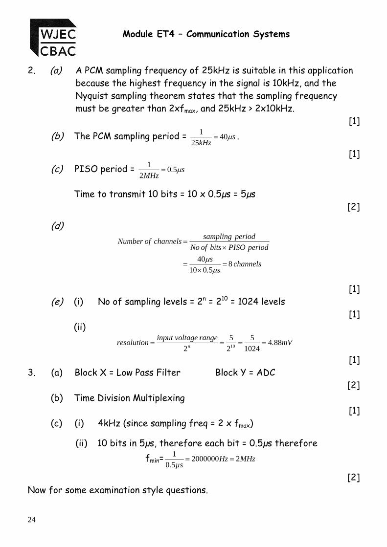
2. (a) A PCM sampling frequency of 25kHz is suitable in this application because the highest frequency in the signal is 10kHz, and the Nyquist sampling theorem states that the sampling frequency must be greater than 2xfmax, and 25kHz > 2x10kHz.
[1] (b) The PCM sampling period = s
kHz40
25
1 .
[1] (c) PISO period = s.
MHz50
2
1
Time to transmit 10 bits = 10 x 0.5µs = 5µs [2]
(d)
channels s.
s
period PISO bits of No
period sampling channels of Number
85010
40
[1] (e) (i) No of sampling levels = 2n = 210 = 1024 levels
[1] (ii)
mV.range voltage input
resolutionn
8841024
5
2
5
2 10
[1] 3. (a) Block X = Low Pass Filter Block Y = ADC
[2] (b) Time Division Multiplexing
[1] (c) (i) 4kHz (since sampling freq = 2 x fmax)
(ii) 10 bits in 5µs, therefore each bit = 0.5µs therefore fmin= MHzHz
µs.22000000
50
1
[2] Now for some examination style questions.

Topic 4.5.4 – Pulse Code Modulation
25
Examination Style Questions
1. Time Division Multiplexing (TDM) can be used to transmit several Pulse Code Modulation (PCM) channels along a single communications link.
Read the passage below and use the information given to answer the questions which follow.
The system uses a PCM sampling gate frequency of 30 kHz to convert audio signals in the range 20 Hz – 12.5 kHz into digital form. A 14-bit code is used to define the sample levels with an input voltage range of 0 to 6V. Several signals are sent along one carrier using TDM. The PISO clock rate of each PCM channel is 1 MHz. A number of PCM channels are transmitted down a single TDM link.
(a) Why is a PCM sampling frequency of 30kHz suitable in this application?
..................................................................................................................................................
..................................................................................................................................................
[1] (b) Calculate the PCM sampling period.
..................................................................................................................................................
[1] (c) Calculate the time needed to transmit a single 14-bit PCM sample at a PISO clock rate of
1MHz.
..................................................................................................................................................
..................................................................................................................................................
[2] (d) Calculate how many PCM channels can be combined using the TDM on the
communication link.
..................................................................................................................................................
..................................................................................................................................................
[1] (e) (i) How many sampling levels are available using a 14 bit code?
..................................................................................................................................................
[1] (ii) Calculate the resolution.
..................................................................................................................................................
..................................................................................................................................................
.................................................................................................................................................. [1]

Module ET4 – Communication Systems
26
2. A PCM communications system consists of a transmitter, a communications link, and a receiver. (a) (i) Draw the block diagram for the transmitter, consisting of the following sub-
systems.
PISO shift register low pass filter ADC Sampling gate 4kHz clock 1MHz clock
[2] (ii) What is the highest signal frequency that this system can process and reproduce it at
the receiver? .....................................................
[1] (iii) Which sub-system cuts out frequencies greater than this ? ........................................................................
[1] (iv) Which block(s) produce a PAM output signal? .........................................................................
[1] (v) What is meant by the resolution of the ADC ? ..................................................................................................................................................
..................................................................................................................................................
..................................................................................................................................................
[2] (vi) The PCM system must cope with an analogue input voltage range of 0 to 10V. The
resolution must be less than 0.01V. What is the minimum number of bits the ADC must output?
.................................................................................................................................................
.................................................................................................................................................
................................................................................................................................................. [2]

Topic 4.5.4 – Pulse Code Modulation
27
(b) The PCM receiver also contains a Schmitt trigger, which has the voltage characteristic shown below.
(i) What is the purpose of this sub-system in the PCM receiver ? ..................................................................................................................................................
..................................................................................................................................................
..................................................................................................................................................
[1] (ii) What are the two switching thresholds for this Schmitt trigger? Upper switching threshold = .............................................. Lower switching threshold = ................................................
[2]

Module ET4 – Communication Systems
28
3. The receiver in a PCM system is made from the following sub-systems:
SIPO shift register low pass filter Schmitt trigger digital-to-analogue converter (DAC) 2MHz clock
Draw the block diagram for this receiver, using these sub-systems.
[3] (b) The circuit diagram shows a 3-bit shift register, made from rising-edge triggered D-type
flip-flops.

Topic 4.5.4 – Pulse Code Modulation
29
Initially all three flip-flops are reset. The upper graph shows the signals applied to the data input and clock input. Use the axes provided to show the corresponding signals at the outputs A,B and C.
(c) The DAC has the following specification. Output voltage range = -5V to +5V Resolution = 1mV What is the smallest number of bits needed for the input in order to meet this specification? ..................................................................................................................................................
..................................................................................................................................................
.................................................................................................................................................. [2]

Module ET4 – Communication Systems
30
4. The block diagram shows part of a Pulse Code Modulation transmitter.
(a) Identify the blocks labelled X, Y and Z. (i) Block X = ............................................... (ii) Block Y = ............................................... (iii) Block Z = ...............................................
[3] (b) The ADC has an 8-bit output and has an input range of 0 – 5.00V. (i) Calculate the resolution for the ADC. ..................................................................................................................................................
..................................................................................................................................................
..................................................................................................................................................
[2] (ii) The input voltage is set to 4.75V. What is the output of the ADC? ..................................................................................................................................................
..................................................................................................................................................
..................................................................................................................................................
[2]

Topic 4.5.4 – Pulse Code Modulation
31
(c) The analogue input signal shown is applied to the above system. The sampling clock signal is also shown.
Complete the following graph to show the output of Block X.
[3]

Module ET4 – Communication Systems
32
5. The following block diagram shows a Pulse Code Modulation (PCM) transmitter.
(a) The output of the Low Pass Filter and the output of Clock A are shown below.
Complete the graph to show the output of the sampling gate.
[3] (b) The signal from the Low Pass Filter contains frequencies in the range 20Hz to 20kHz. (i) What is the relationship between the input signal frequency range and the minimum
sampling frequency required to allow the signal from the Low Pass Filter to be reconstructed at the receiver?
..................................................................................................................................................
(ii) Hence, what is the minimum frequency that can be used for Clock A in this transmitter?
..................................................................................................................................................
[2]

Topic 4.5.4 – Pulse Code Modulation
33
(c) Clock B must operate at a higher frequency than Clock A for the system to work properly. Explain why this is the case.
..................................................................................................................................................
..................................................................................................................................................
..................................................................................................................................................
..................................................................................................................................................
..................................................................................................................................................
[1] (d) For this system, the analogue to digital converter (ADC) has an input voltage range of 0 to
4V. (i) How many voltage levels are provided by the ADC? .................................................................................................................................................
.................................................................................................................................................
(ii) What is the resolution of the system? .................................................................................................................................................
................................................................................................................................................. [2]
(e) A PCM receiver requires a serial-in-parallel-out shift register (SIPO) which can be constructed using D-Type flip-flops.
On the diagram above:
(i) draw the connections needed to make the first four bits of a SIPO shift register. [2]
(ii) mark clearly where the input signal is connected; [1]
(iii) mark clearly where the output signal is obtained from. [1]

Module ET4 – Communication Systems
34
6. The following block diagram shows a Pulse Code Modulation (PCM) transmitter.
(a) The output of the Low Pass Filter and the output of Clock A are shown below.
Complete the graph to show the output of the sampling gate.
[3]

Topic 4.5.4 – Pulse Code Modulation
35
(b) The signal from the low pass filter contains frequencies in the range 100Hz – 4kHz. (i) What is the relationship between the input signal frequency range and the minimum
sampling frequency required to allow the signal from the low pass filter to be reconstructed at the receiver ?
......................................................................................................................................
[1] (ii) Hence, what is the minimum frequency that can be used for Clock A in this
transmitter. ......................................................................................................................................
[1] (c) Clock B must operate at a higher frequency that clock A for the system to work properly.
Explain why this is the case. .................................................................................................................................................
..................................................................................................................................................
..................................................................................................................................................
..................................................................................................................................................
..................................................................................................................................................
[1] (d) The 12-bit analogue to digital converter (ADC) has an input voltage range of 0-6V. (i) How many sampling (voltage) levels are provided by the ADC? ..................................................................................................................................................
..................................................................................................................................................
[1]
(ii) What is the resolution of the system? ..................................................................................................................................................
..................................................................................................................................................
[1]

Module ET4 – Communication Systems
36
7. The block diagram below shows a transmitter for a Pulse Code Modulation (PCM) system which is used in a telephone exchange.
(a) Complete the block diagram by correctly labelling the missing blocks.
[3]
(b) The highest frequency present in the input signal is 4 kHz. Choose from the list of possible frequencies below two frequencies that could be used for clock A to enable the signal to be regenerated without distortion.
1.0kHz 1.5kHz 4.0kHz 5.5kHz
7.0kHz 8.5kHz 10.0kHz
Frequency 1: ............................................... Frequency 2: ...............................................
[2]
(c) Several PCM systems can be combined using Time Division Multiplexing. Explain what is meant by Time Division Multiplexing. ..................................................................................................................................................
..................................................................................................................................................
..................................................................................................................................................
..................................................................................................................................................
..................................................................................................................................................
..................................................................................................................................................
[2]

Topic 4.5.4 – Pulse Code Modulation
37
8. The receiver of a Pulse Code Modulation system is constructed from the following subsystems.
SIPO Shift Register 2MHz Clock Schmitt trigger Low pass filter Digital to Analogue Converter (DAC)
(a) Draw the block diagram for this receiver, using only these sub-systems.
[2] (b) The following graphs show the output of two sub-systems in the PCM receiver.
(i) Which sub-system produces the output shown by Graph A? ..................................................................................................................................................
[1] (ii) Which sub-system produces the output shown by Graph B? ..................................................................................................................................................
[1]

Module ET4 – Communication Systems
38
9. The block diagram shows part of a Pulse Code Modulation transmitter.
(a) Identify the blocks labelled X, Y and Z. (i) Block X = ............................................... (ii) Block Y = ............................................... (iii) Block Z = ...............................................
[3] (b) The ADC has an 10-bit output and has an input range of 0 – 5.00V. (i) Calculate the resolution for the ADC. ..................................................................................................................................................
..................................................................................................................................................
..................................................................................................................................................
[2] (ii) The input voltage is set to 2.44V. What is the output of the ADC? ..................................................................................................................................................
..................................................................................................................................................
..................................................................................................................................................
[2]

Topic 4.5.4 – Pulse Code Modulation
39
(c) The analogue input signal shown is applied to the above system. The sampling clock signal is also shown.
Complete the following graph to show the output of Block X.
[3]

Module ET4 – Communication Systems
40
Self Evaluation Review
Learning Objectives My personal review of these objectives:
analyse and draw graphs to illustrate pulse amplitude modulation (PAM) techniques;
relate required sampling frequency to the highest frequency in the signal;
draw a block diagram for, and describe the operation of, a PCM communication system consisting of;
transmitter low pass filter sampling gate sampling clock ADC PISO shift register PISO clock
receiver Schmitt trigger SIPO shift register SIPO clock DAC low pass filter
relate resolution to the number of sampling levels, and select and use the formula:
n
range voltage inputresolution
2
describe how time division multiplexing (TDM) can be used to improve the capacity of a PCM communications link, using TDM.
Targets: 1. ……………………………………………………………………………………………… ………………………………………………………………………………………………
2. ………………………………………………………………………………………………
………………………………………………………………………………………………