5-v low drop voltage regulator tle 4267
TRANSCRIPT

5-V Low Drop Voltage Regulator
TLE 4267
Data Sheet 1 Rev. 2.5, 2007-03-20
Type Package Type Package
TLE 4267 PG-TO220-7-11 TLE 4267 S PG-TO220-7-12
TLE 4267 G PG-TO263-7-1 TLE 4267 GM PG-DSO-14-30
P-TO220-7-3
P-TO 220-7-180(TO-220 AB/7, Option E3180)
P-TO220-7-230
P-DSO-14-3, -8, -9, -11, 14
Features
• Output voltage tolerance ≤ ±2%• 400 mA output current capability• Low-drop voltage• Very low standby current consumption• Input voltage up to 40 V• Overvoltage protection up to 60 V (≤ 400 ms)• Reset function down to 1 V output voltage• ESD protection up to 2000 V• Adjustable reset time• On/off logic• Overtemperature protection• Reverse polarity protection• Short-circuit proof• Wide temperature range• Suitable for use in automotive electronics• Green Product (RoHS compliant)• AEC Qualified
Functional Description
TLE 4267 is a 5-V low drop voltage regulator forautomotive applications in the PG-TO220-7 orPG-DSO-14-30 package. It supplies an output current of> 400 mA. The IC is shortcircuit-proof and has anovertemperature protection circuit.
Data Sheet 2 Rev. 2.5, 2007-03-20
TLE 4267
Application
The IC regulates an input voltage VI in the range of 5.5 V < VI < 40 V to a nominal outputvoltage of VQ = 5.0 V. A reset signal is generated for an output voltage of VQ < VRT (typ.4.5 V). The reset delay can be set with an external capacitor. The device has two logicinputs. A voltage of VE2 > 4.0 V given to the E2-pin (e.g. by ignition) turns the device on.Depending on the voltage on pin E6 the IC may be hold in active-state even if VE2 goesto low level. This makes it simple to implement a self-holding circuit without externalcomponents. When the device is turned off, the output voltage drops to 0 V and currentconsumption tends towards 0 µA.
Design Notes for External Components
The input capacitor CI is necessary for compensation of line influences. The resonantcircuit consisting of lead inductance and input capacitance can be damped by a resistorof approx. 1 Ω in series with CI. The output capacitor is necessary for the stability of theregulating circuit. Stability is guaranteed at values of ≥ 22 µF and an ESR of ≤ 3 Ω withinthe operating temperature range.
Circuit Description
The control amplifier compares a reference voltage, which is kept highly accurate byresistance adjustment, to a voltage that is proportional to the output voltage and drivesthe base of the series transistor via a buffer. Saturation control as a function of the loadcurrent prevents any over-saturating of the power element.
The reset output RO is in high-state if the voltage on the delay capacitor CD is greater orequal VUD. The delay capacitance CD is charged with the current ID for output voltagesgreater than the reset threshold VRT. If the output voltage gets lower than VRT a fastdischarge of the delay capacitor CD sets in and as soon as VCD gets lower than VLD thereset output RO is set to low-level (see Figure 6). The reset delay can be set within widerange by dimensioning the capacitance of the external capacitor.

TLE 4267
Data Sheet 3 Rev. 2.5, 2007-03-20
Inhibit: E2 Enable function, active HighHold: E6 Hold and release function, active Low
Table 1 Truth Table for Turn-ON/Turn-OFF Logic
E2, Inhibit
E6,Hold
VQ Remarks
L X OFF Initial state, Inhibit internally pulled-up
H X ON Regulator switched on via Inhibit, by ignition for example
H L ON Hold clamped active to ground by controller while Inhibit is still high
X L ON Previous state remains, even ignition is shut off: self-holding state
L L ON Ignition shut off while regulator is in self-holding state
L H OFF Regulator shut down by releasing of Hold while Inhibit remains Low, final state. No active clamping required by external self-holding circuit (µC) to keep regulator in off-state.

Data Sheet 4 Rev. 2.5, 2007-03-20
TLE 4267
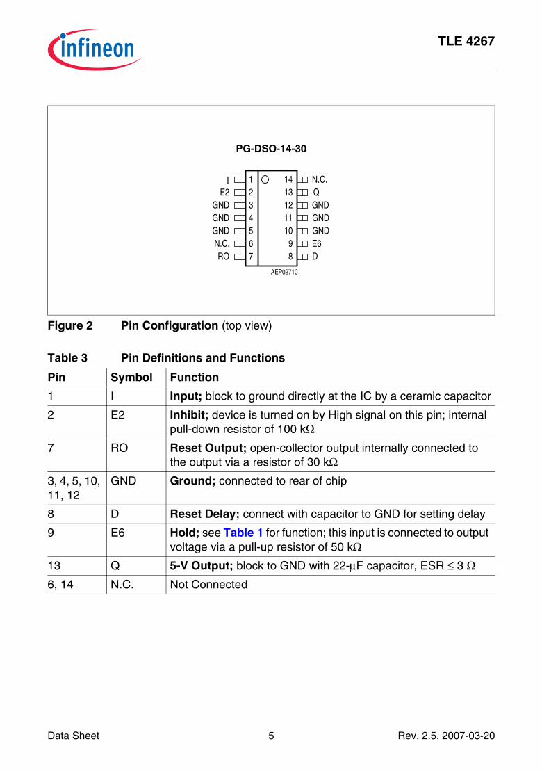
Figure 1 Pin Configuration (top view)
Table 2 Pin Definitions and Functions
Pin Symbol Function
1 I Input; block to ground directly at the IC by a ceramic capacitor
2 E2 Inhibit; device is turned on by High signal on this pin; internal pull-down resistor of 100 kΩ
3 RO Reset Output; open-collector output internally connected to the output via a resistor of 30 kΩ
4 GND Ground; connected to rear of chip
5 D Reset Delay; connect via capacitor to GND
6 E6 Hold; see Table 1 for function; this input is connected to output voltage via a pull-up resistor of 50 kΩ
7 Q 5-V Output; block to GND with 22-µF capacitor, ESR < 3 Ω
AEP02123
ΙE2
ROGND
D Q
4321 5 6 7
E6AEP01481
ΙE2
ROGND
D Q
4321 5 6 7
E6
PG-TO220-7-11 PG-TO220-7-12
7651 2 3 4
AEP01724E6
QDGND
ROE2
Ι
PG-TO263-7-1
TLE 4267
Data Sheet 5 Rev. 2.5, 2007-03-20
Figure 2 Pin Configuration (top view)
Table 3 Pin Definitions and Functions
Pin Symbol Function
1 I Input; block to ground directly at the IC by a ceramic capacitor
2 E2 Inhibit; device is turned on by High signal on this pin; internal pull-down resistor of 100 kΩ
7 RO Reset Output; open-collector output internally connected to the output via a resistor of 30 kΩ
3, 4, 5, 10, 11, 12
GND Ground; connected to rear of chip
8 D Reset Delay; connect with capacitor to GND for setting delay
9 E6 Hold; see Table 1 for function; this input is connected to output voltage via a pull-up resistor of 50 kΩ
13 Q 5-V Output; block to GND with 22-µF capacitor, ESR ≤ 3 Ω6, 14 N.C. Not Connected
PG-DSO-14-30
AEP02710
E6
GND
N.C.
N.C.RO
GNDQ
109
GND GND
12345
GND
67 D
14131211
E2
GND
8
Ι

Data Sheet 6 Rev. 2.5, 2007-03-20
TLE 4267
Figure 3 Block Diagram
AEB01482
SaturationControl and
Protection Circuit
Turn-ON/Turn-OFFLogic
ResetGenerator
BufferControl
Amplifier
Sensor
Q
D
R
E2Ground
OutputReset
DelayReset
OutputInputΙ
Temperature
ReferenceBandgap
Adjustment
5 V
HoldInhibitGNDE6

TLE 4267
Data Sheet 7 Rev. 2.5, 2007-03-20
Table 4 Absolute Maximum Ratings
TJ = -40 to 150 °C
Parameter Symbol Limit Values Unit Notes
Min. Max.
Input
Voltage VI -42 42 V –
Voltage VI – 60 V t ≤ 400 ms
Current II – – – internally limited
Reset Output
Voltage VRO -0.3 7 V –
Current IRO – – – internally limited
Reset Delay
Voltage VD -0.3 42 V –
Current ID – – – –
Output
Voltage VQ -0.3 7 V –
Current IQ – – – internally limited
Inhibit
Voltage VE2 -42 42 V –
Current IE2 -5 5 mA t ≤ 400 ms
Hold
Voltage VE6 -0.3 7 V –
Current IE6 – – mA internally limited
GND
Current IGND -0.5 – A –
Temperatures
Junction temperature TJ – 150 °C –
Storage temperature Tstg -50 150 °C –

Data Sheet 8 Rev. 2.5, 2007-03-20
TLE 4267
Table 5 Operating Range
Parameter Symbol Limit Values Unit Notes
Min. Max.
Input voltage VI 5.5 40 V see diagram
Junction temperature TJ -40 150 °C –
Thermal Resistance
Junction ambient Rthja – 65 K/W PG-TO220-7-11 package
Junction-case Rthjc – 6 K/W PG-TO220-7-11 package
Junction-case Zthjc – 2 K/W T < 1 msPG-TO220-7-11 package
Junction ambient Rthja – 70 K/W PG-TO263-7-1 (SMD) package
Junction-case Rthjc – 6 K/W PG-TO263-7-1 (SMD) package
Junction-case Zthjc – 2 K/W T < 1 msPG-TO263-7-1 (SMD) package
Junction ambient Rthja – 65 K/W PG-TO220-7-12 package
Junction-case Rthjc – 6 K/W PG-TO220-7-12 package
Junction-case Zthjc – 2 K/W T < 1 msPG-TO220-7-12 package
Junction ambient Rthja – 70 K/W PG-DSO-14-30 package
Junction-pin Rthjp – 30 K/W PG-DSO-14-30 package

TLE 4267
Data Sheet 9 Rev. 2.5, 2007-03-20
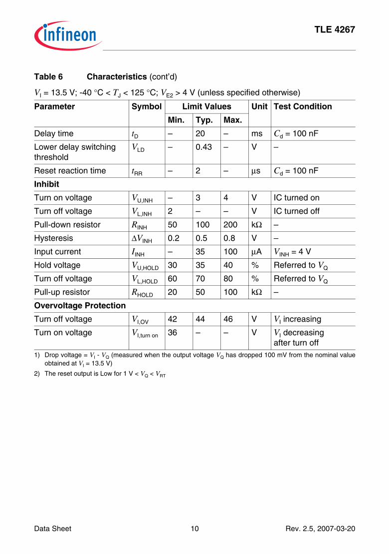
Table 6 Characteristics
VI = 13.5 V; -40 °C < TJ < 125 °C; VE2 > 4 V (unless specified otherwise)
Parameter Symbol Limit Values Unit Test Condition
Min. Typ. Max.
Output voltage VQ 4.9 5 5.1 V 5 mA ≤ IQ ≤ 400 mA6 V ≤ VI ≤ 26 V
Output voltage VQ 4.9 5 5.1 V 5 mA ≤ IQ ≤ 150 mA6 V ≤ VI ≤ 40 V
Output current limiting IQ 500 – – mA TJ = 25 °CCurrent consumptionIq = II - IQ
Iq – – 50 µA IC turned off
Current consumptionIq = II - IQ
Iq – 1.0 10 µA TJ = 25 °CIC turned off
Current consumptionIq = II - IQ
Iq – 1.3 4 mA IQ = 5 mAIC turned on
Current consumptionIq = II - IQ
Iq – – 60 mA IQ = 400 mA
Current consumptionIq = II - IQ
Iq – – 80 mA IQ = 400 mAVI = 5 V
Drop voltage VDr – 0.3 0.6 V IQ = 400 mA1)
Load regulation ∆VQ – – 50 mV 5 mA ≤ IQ ≤ 400 mA
Supply-voltage regulation
∆VQ – 15 25 mV VI = 6 to 36 V;IQ = 5 mA
Supply-voltage rejection SVR – 54 – dB fr = 100 Hz;Vr = 0.5 Vpp
Longterm stability ∆VQ – 0 – mV 1000 h
Reset Generator
Switching threshold VRT 4.2 4.5 4.8 V –
Reset High level – 4.5 – – V Rext = ∞Saturation voltage VRO,SAT – 0.1 0.4 V RR = 4.7 kΩ 2)
Internal Pull-up resistor RRO – 30 – kΩ –
Saturation voltage VD,SAT – 50 100 mV VQ < VRT
Charge current ID 8 15 25 µA VD = 1.5 V
Upper delay switching threshold
VUD 2.6 3 3.3 V –
Data Sheet 10 Rev. 2.5, 2007-03-20
TLE 4267
Delay time tD – 20 – ms Cd = 100 nF
Lower delay switching threshold
VLD – 0.43 – V –
Reset reaction time tRR – 2 – µs Cd = 100 nF
Inhibit
Turn on voltage VU,INH – 3 4 V IC turned on
Turn off voltage VL,INH 2 – – V IC turned off
Pull-down resistor RINH 50 100 200 kΩ –
Hysteresis ∆VINH 0.2 0.5 0.8 V –
Input current IINH – 35 100 µA VINH = 4 V
Hold voltage VU,HOLD 30 35 40 % Referred to VQ
Turn off voltage VL,HOLD 60 70 80 % Referred to VQ
Pull-up resistor RHOLD 20 50 100 kΩ –
Overvoltage Protection
Turn off voltage VI,OV 42 44 46 V VI increasing
Turn on voltage VI,turn on 36 – – V VI decreasing after turn off
1) Drop voltage = VI - VQ (measured when the output voltage VQ has dropped 100 mV from the nominal valueobtained at VI = 13.5 V)
2) The reset output is Low for 1 V < VQ < VRT
Table 6 Characteristics (cont’d)
VI = 13.5 V; -40 °C < TJ < 125 °C; VE2 > 4 V (unless specified otherwise)
Parameter Symbol Limit Values Unit Test Condition
Min. Typ. Max.

TLE 4267
Data Sheet 11 Rev. 2.5, 2007-03-20
Figure 4 Test Circuit
Figure 5 Application Circuit
AES01483
22 F
ΙQ
ΙRO
VE6
Ω4.7 k
D
RO
QΙ
E2Ι
1000 F 470 nF
Ι Ι
VE2DCVC
GNDΙdΙVR
QVVΙ
TLE 4267µ µ
Inhibit
GND Hold
AES01484
22 Fµ
GND
R
Q
R
Ι
470 nF
From Cµ
100 nF
5 V Output
E2; egfrom Terminal 15
to µC
Input
Reset
4267TLEInhibit
Hold

Data Sheet 12 Rev. 2.5, 2007-03-20
TLE 4267
Figure 6 Time Response
AET01985
t D
t RR
RRt<
PowerReset Shutdown
Thermal Voltage Dropat Input
Undervoltageat Output
SecondarySpike Bounce
Load Shutdownon
VRO, SAT
LDVUDV
VD, SAT
RTV
L, INHV
VU, INH
INHV
ROV
VD
QV
ΙV
t
t
t
t
t
=dtVd D
DC
Ι

TLE 4267
Data Sheet 13 Rev. 2.5, 2007-03-20
Figure 7 Enable and Hold Behavior
AET01986
V
Enable inactive, clamped by int.
V
pull-down resistor
GND by externalHold active, clamped toPower-ON reset
5)
4)3)
Cµ
V
Hold inactive, pulled up by Enable active
VRO, SAT
2)1)
RO
3)
t D
LDVVD, SAT
UDV
V
RT
D
E6
E6V
Voltage controller shutdown
10)9)8)
µwas released toNo switch on viaOutput-low reset
than 4 sV for more
possible after E6E6, relV>
Hold inactive, released byPulse width smaller than
7)6)
Q
t
Cs
µ1 µ
9)
RR
8)
E6V
V
Q, NOMV
Q
U, HOLDV
L, HOLDV2)
1)
µ
4) 6)
<1 s
5)
µ
7)10)
10< s
VΙ
E2V
U, INH
L, INHV
V
t
t
t
t
t
t

Data Sheet 14 Rev. 2.5, 2007-03-20
TLE 4267
Output Voltage VQ versusTemperature Tj
Charge Current ID versusTemperature Tj
Drop Voltage VDr versusOutput Current IQ
Delay Switching Threshold VUD versusTemperature Tj
AED01486
-404.70
Q
T
V Ι =
5.10
V
4.80
4.90
5.00
13.5 V
C0 40 80 160
V
j
AED01485
-40
ΙD
T
V Ι = 13.5 V
C0 40 80 160
A
VC = 0 V
µ
10
12
14
16
18
22
DΙ
j
AED01488
00
Ι Q
CT
125 C
= 25
=T
100
200
300
400
500
mV
700
100 200 300 400 mA 600
DrV
j
j
AED01487
-400
UD
T
V Ι = 13.5 V
C0 40 80 160
0.5
1.0
1.5
2.0
2.5
3.0
V
4.0
VUD
V
j
Data Sheet 15 Rev. 2.5, 2007-03-20
TLE 4267
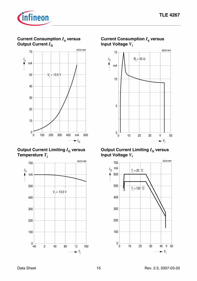
Current Consumption Iq versusOutput Current IQ
Output Current Limiting IQ versusTemperature Tj
Current Consumption Iq versusInput Voltage VI
Output Current Limiting IQ versusInput Voltage VI
AED01490
00
Ι Q
10
20
30
40
50
mA
70
100 200 300 400 mA 600
Ι q
V Ι = 13.5 V
AED01489
-40
ΙQ
T
C0 40 80 160
mA
100
200
300
400
500
700
0
13.5 V=ΙV
j
AED01491
00
qΙ =
10 20 30 50
RL
ΙV
V
Ω25
5
10
mA
15
00
AED01987
Ι Q
V
V
i
mA
100
200
300
400
500
600
700
10 20 30 40 50
125 C=
= C25
jT
jT

Data Sheet 16 Rev. 2.5, 2007-03-20
TLE 4267
Output Voltage VQ versusInhibit Voltage VINH
Inhibit Current IINH versusInhibit Voltage VINH
00
AED01988
VQ
2
4
V
6
1
3
5
INHV
1 2 3 4 5 6V0
0
AED01989
Ι INH
V
V
INH
1 2 3 4 5 6
10
20
30
40
50
Aµ

TLE 4267
Data Sheet 17 Rev. 2.5, 2007-03-20
Package Outlines
Figure 8 PG-TO220-7-11 (Plastic Transistor Single Outline)
Green Product (RoHS compliant)
To meet the world-wide customer requirements for environmentally friendly productsand to be compliant with government regulations the device is available as a greenproduct. Green products are RoHS-Compliant (i.e Pb-free finish on leads and suitablefor Pb-free soldering according to IPC/JEDEC J-STD-020).
Typical
±0.11.27
4.4
9.25
±0.20.05
1)
All metal surfaces tin plated, except area of cut.
2.4
0.5 ±0.1
±0.3
8.6
10.2
±0.3
±0.43.9
±0.48.4
3.7±
0.3
A
A0.25 M
9.8 ±0.15
2.8
1)
15.6
5±0.
3
13.4
0...0.15
1.27
0.6 ±0.1
C
±0.2
17±0
.3
8.5 1)
9.9 ±0.2
7x
-0.1
53.
7
10 ±0.2
6x
C
1.6±
0.3
GPT09083
You can find all of our packages, sorts of packing and others in ourInfineon Internet Page “Products”: http://www.infineon.com/products.
Dimensions in mmSMD = Surface Mounted Device

Data Sheet 18 Rev. 2.5, 2007-03-20
TLE 4267
Figure 9 PG-TO263-7-1 (Plastic Transistor Single Outline)
Green Product (RoHS compliant)
To meet the world-wide customer requirements for environmentally friendly productsand to be compliant with government regulations the device is available as a greenproduct. Green products are RoHS-Compliant (i.e Pb-free finish on leads and suitablefor Pb-free soldering according to IPC/JEDEC J-STD-020).
A
BA0.25 M
0.1
Typical
±0.210
8.5 1)
7.55
1)
(15)
±0.2
9.25
±0.3
1
0...0.15
7 x 0.6 ±0.1
±0.1
GPT09114
1.27
4.4
B
0.5 ±0.1±0
.32.
7
4.7±
0.5
0.05
1)
0.1
Metal surface min. X = 7.25, Y = 6.9
2.4
1.27
All metal surfaces tin plated, except area of cut.
0...0.3
B
6 x8˚ MAX.
You can find all of our packages, sorts of packing and others in ourInfineon Internet Page “Products”: http://www.infineon.com/products.
Dimensions in mmSMD = Surface Mounted Device
TLE 4267
Data Sheet 19 Rev. 2.5, 2007-03-20
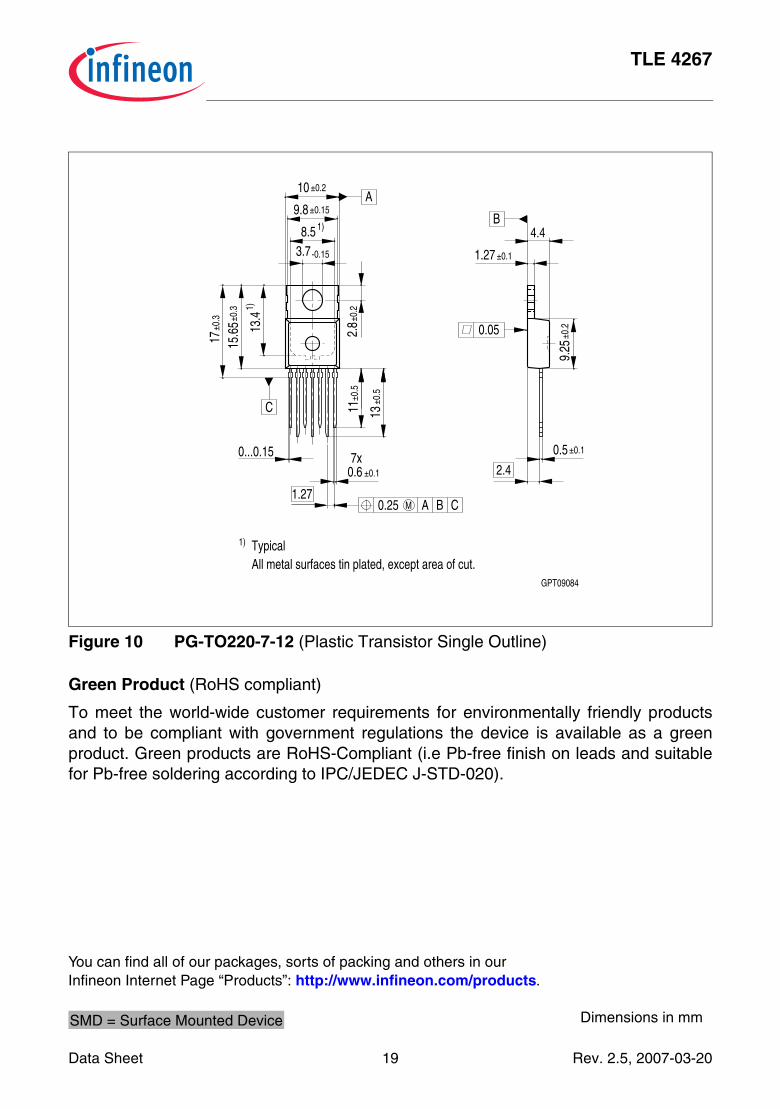
Figure 10 PG-TO220-7-12 (Plastic Transistor Single Outline)
Green Product (RoHS compliant)
To meet the world-wide customer requirements for environmentally friendly productsand to be compliant with government regulations the device is available as a greenproduct. Green products are RoHS-Compliant (i.e Pb-free finish on leads and suitablefor Pb-free soldering according to IPC/JEDEC J-STD-020).
GPT09084
A
BA0.25 M
Typical
9.8 ±0.15
2.8
1)
15.6
5±0.
3
13.4
0...0.15
1.27
0.6 ±0.1
±0.11.27
4.4B
9.25
±0.20.05
1)
All metal surfaces tin plated, except area of cut.
C
±0.2
17±0
.3
8.5 1)
10 ±0.2
3.7-0.15
C
2.4
0.5 ±0.1
13±0
.5±0.5
11
7x
You can find all of our packages, sorts of packing and others in ourInfineon Internet Page “Products”: http://www.infineon.com/products.
Dimensions in mmSMD = Surface Mounted Device

Data Sheet 20 Rev. 2.5, 2007-03-20
TLE 4267
Figure 11 PG-DSO-14-30 (Plastic Dual Small Outline)
Green Product (RoHS compliant)
To meet the world-wide customer requirements for environmentally friendly productsand to be compliant with government regulations the device is available as a greenproduct. Green products are RoHS-Compliant (i.e Pb-free finish on leads and suitablefor Pb-free soldering according to IPC/JEDEC J-STD-020).
1) Does not include plastic or metal protrusion of 0.15 max. per side2) Lead width can be 0.61 max. in dambar area
-0.28.75 1)
0.64
0.19
+0.0
6
Index Marking
1.27
+0.100.410.1
1
14
2)
7
14x
8
0.17
5
(1.4
7)
±0.0
7
±0.26
0.35 x 45˚
-0.2
1.75
MA
X.
41)
±0.25
8˚M
AX
.
-0.06 0.2 M A BM0.2 C
C
B
A
GPS01230
You can find all of our packages, sorts of packing and others in ourInfineon Internet Page “Products”: http://www.infineon.com/products.
Dimensions in mmSMD = Surface Mounted Device

TLE 4267
Revision History
Data Sheet 21 Rev. 2.5, 2007-03-20
Version Date Changes
Rev. 2.5 2007-03-20 Initial version of RoHS-compliant derivate of TLE 4267Page 1: AEC certified statement addedPage 1 and Page 17 ff: RoHS compliance statement and Green product feature addedPage 1 and Page 17 ff: Package changed to RoHS compliant versionLegal Disclaimer updated

Edition 2007-03-20Published byInfineon Technologies AG81726 Munich, Germany© 2007 Infineon Technologies AGAll Rights Reserved.
Legal DisclaimerThe information given in this document shall in no event be regarded as a guarantee of conditions or characteristics. With respect to any examples or hints given herein, any typical values stated herein and/or any information regarding the application of the device, Infineon Technologies hereby disclaims any and all warranties and liabilities of any kind, including without limitation, warranties of non-infringement of intellectual property rights of any third party.
InformationFor further information on technology, delivery terms and conditions and prices, please contact the nearest Infineon Technologies Office (www.infineon.com).
WarningsDue to technical requirements, components may contain dangerous substances. For information on the types in question, please contact the nearest Infineon Technologies Office.Infineon Technologies components may be used in life-support devices or systems only with the express written approval of Infineon Technologies, if a failure of such components can reasonably be expected to cause the failure of that life-support device or system or to affect the safety or effectiveness of that device or system. Life support devices or systems are intended to be implanted in the human body or to support and/or maintain and sustain and/or protect human life. If they fail, it is reasonable to assume that the health of the user or other persons may be endangered.