642 …xs3d.kaist.ac.kr/paperdata/j23-ieee tase-park, morrison-controll wafer... ·...
TRANSCRIPT

642 IEEE TRANSACTIONS ON AUTOMATION SCIENCE AND ENGINEERING, VOL. 12, NO. 2, APRIL 2015
Controlled Wafer Release in ClusteredPhotolithography Tools: Flexible Flow Line
Job Release Scheduling and an LMOLP HeuristicKyungsu Park and James R. Morrison, Member, IEEE
Abstract—As a clustered photolithography tool (CPT) in semi-conductor wafer manufacturing can cost as much as US$100million, it must be operated efficiently. To maximize throughput,wafers are generally admitted to a CPT opportunistically, that is,as soon as they are available and the tool can accept them. Here,our goal is to develop release methods that retain throughputbut increase manufacturing agility. As Petri net methods proveintractable, we develop a heuristic based on the use of flexible flowline models for the CPT. Such models are appropriate when thetool throughput for each class of wafers is dictated by the bottle-neck process time plus unavoidable robot handling overhead. Theheart of the heuristic is a lexicographic multiple objective linearprogram (LMOLP). It first ensures that wafers exit the tool asearly as possible and subsequently delays the wafer admission tominimize the mean residency time.To test the efficacy of the release policy, we conduct numerical
experiments on detailed CPT models based on industry data. Themodel includes many features of real world tools such as wafertransport robots, an industry-based robot scheduling policy, a pre-scan track buffer, reticle setups, and track setups. As compared tothe commonly used opportunistic wafer admission, the heuristicprovides statistically indistinguishable throughput with significantreductions in wafer residency time, in-tool buffer occupation, andhot lot cycle time. We conduct a numerical robustness study to as-sess the performance of the release policy when the system modelused in the LMOLP deviates significantly from the behavior in theCPT. The LMOLP heuristic continues to perform well in the pres-ence of such disturbances.
Note to Practitioners—In clustered photolithography tools(CPTs) in semiconductor wafer manufacturing, wafers are com-monly admitted to the tool as soon as the wafer handling robot canreceive one. While this is done to ensure maximum throughput, itcan result in long wafer residency in the tool and a reduction inthe ability to promptly serve arriving hot lots. Here, we developa computationally tractable and practical linear programmingbased method to obtain more judicious wafer admission times.Detailed simulation studies of models of real CPTs demonstrateno loss of throughput and a 52%, 31%, and 23% improvementin wafer time in the tool, lot time in the tool and hot lot cycle
Manuscript received December 06, 2013; revised February 15, 2014;accepted March 05, 2014. Date of publication April 07, 2014; date of currentversion April 03, 2015. This paper was recommended for publication byAssociate Editor N. Wu and Editor H. Ding upon evaluation of the reviewers'comments. This work was supported in part by the Korea Research Foundation(KRF) under Grant NRF-2009-0077673 and Grant NRF-2010-0005577, and inpart by the KAIST Institute under Grant N10080019. (Corresponding author:J. R. Morrison.)The authors are with the Department of Industrial and Systems Engineering,
Korea Advanced Institute of Science and Technology (KAIST), Daejeon 305-701, South Korea (email: [email protected]; [email protected]).Color versions of one or more of the figures in this paper are available online
at http://ieeexplore.ieee.org.Digital Object Identifier 10.1109/TASE.2014.2311997
time, respectively. The results are robust; when the CPT exhibitsbehaviors significantly different than assumed in the controller,the release policy continues to perform well. As such, the methodmay prove useful in practical contexts to reduce wafer residencytime and increase CPT agility.Index Terms—Clustered photolithography tools, flexible flow
lines, job release scheduling, lexicographic multiple objectivelinear programming, semiconductor wafer manufacturing.
I. INTRODUCTION
C LUSTERED photolithography tools (CPTs) are by far themost expensive tools in the typically US$5 billion [1]
semiconductor wafer fabrication facilities and often serve asthe production bottleneck. As they must thus be operated ef-ficiently, wafers are typically admitted to the CPT opportunis-tically. While this ensures maximum throughput, wafers canspend much longer in the tool than necessary. The CPT may notbe able to respond to the arrival of hot lots as promptly. Here,we develop methods to more carefully admit wafers to CPTsthat provide statistically indistinguishable throughput but miti-gate the drawbacks of opportunistic admission.
A. Clustered Photolithography ToolsA CPT consists of three conceptual sections; refer to Fig. 1.
(A detailed CPT model is discussed in Section II-A.) The pre-scan processes, or pre-scan track, coat the wafer with a photo-sensitive material. The photolithography scanner exposes eachwafer to a pattern of light. The post-scan processes, or post-scan track, then develop the pattern. Wafers are advanced fromprocess to process by wafer handling robots. The scanner is themost expensive section and generally the CPT bottleneck.A setup of the pre-scan track may be required when changing
from one type of wafer lot to another (a lot is a batch of identicalwafers). A pre-scan buffer is used to store wafers and supplythem to the scanner during this setup. A post-scan track setupmay be required, but this can often be practically ignored sincea reticle alignment setup at the scanner eclipses the post-scantrack setup.1) Unnecessarily Early Wafer Admission: While the wafer
admission policy for CPTs may depend on tool, technology andfab, it is common to admit wafers opportunistically. Wafers areadvanced when the wafer handling robot, process module andwafer are jointly available. This fills the pre-scan buffer andserves to maximize throughput, but early wafer admission hasconsequences:
i) Deployment opportunity [2] of the lot is reduced.
1545-5955 © 2014 IEEE. Personal use is permitted, but republication/redistribution requires IEEE permission.See http://www.ieee.org/publications_standards/publications/rights/index.html for more information.

PARK AND MORRISON: CONTROLLED WAFER RELEASE IN CLUSTERED PHOTOLITHOGRAPHY TOOLS 643
Fig. 1. Conceptual diagram of a CPT.
ii) Subsequent high-priority hot lots may experience addi-tional queueing behind a lot that was admitted too early.
iii) The number of wafers in the pre-scan buffer and tool,and the wafer duration in the tool, may be greater thanrequired.
Consequences (i) and (ii) reduce manufacturing agility. Conse-quence (iii) may relate to yield; delays in the CPT may increasecontamination probability. Some believe that longer cycle timesare correlated with lower yield; see [3]–[9].This issue has been highlighted in a concept paper from IBM
research [10]. Concerned about work-in-process inventory(WIP), they considered when to load products into a printedcircuit board production line. They used a flexible flow line(FFL) to model their system and informally considered thetimely admission problem. They focused on periodic operationand did not consider setups between different products.2) Challenges of Tool Scheduling: Ideally, we could model
and optimize the CPT with its wafer transport robots. There isa wealth of research about the cyclic or periodic behavior (alsoreferred to as steady-state behavior in the cluster tool sched-uling literature) of equipment with wafer handling robots; see[11]–[19]. However, in general and with increasing prominence[20], CPTs operate in an acyclic mode (this is often referredto as transient in the cluster tool scheduling literature). As weshall see, the computational complexity of transient schedulingof wafer transport robots is high [14]. A more tractable modelis needed for practice.In addition, process times and robotic task times may have
variation [21]–[23], which further increases the computationalcomplexity. Thus, heuristic dispatching schemes, such as thelongest waiting pair (LWP) rule, are often used for robot sched-uling in practice [14], [24].We will first employ recent Petri net methods to address the
combined wafer release and wafer transport robot schedulingproblem. However, as we shall see, the computation required isprohibitive. As such, we will decouple the wafer admission andwafer transport robot scheduling problems. For the wafer admis-sion problem, we employ a flexible flow line (FFL) model of theCPT (which assumes its wafer throughput capacity is dictatedby the bottleneck process time plus unavoidable robot handlingoverhead time; this is often referred to as process bound). Theresulting release times can be used to direct when the underlyingwafer handling robot controller should be allowed to consider awafer for admission.The FFL relaxation accounts for wafer transport robots solely
as an addition to the process times. This is reasonable only if
Fig. 2. A flexible flow line.
the CPT is process bound. By process bound, we mean that thetool throughput for a given class of wafers is dictated by thebottleneck process time plus unavoidable robot overhead. AsCPTs can cost US$120 million [25], it is unwise to be robotbound. As discussed in the literature, cluster tools are oftenprocess bound (see [16], [26], and [27]; they also discuss de-tailed definitions for resource workload which is used to deter-mine if a tool is process or robot bound). Such FFL models canpredict throughput and cycle time values of practical CPTs towithin 1.0% and 4.0%, respectively [28]. Many practical studiesuse flow line models to analyze, schedule lots for and optimizeCPTs; cf. [29]–[34].
B. Flexible Flow Line SchedulingFlexible flow lines (FFLs) can serve as models of practical
equipment or production. A flow line consists of a sequence ofprocesses or stages that are conducted one after the other onincoming jobs. A buffer for waiting jobs and a dedicated serverare provided for each process. In an FFL, multiple servers ormodules may be devoted to each process. Refer to Fig. 2.Typical FFL scheduling problems determine the sequence
and timing of jobs on each server to minimize the makespan;it is an NP-hard problem [35]. This is true even for a simpleFFLwith two process stages and finite intermediate buffers [36].To address this computational complexity, heuristics for variousobjective functions have been proposed; cf. [3], [37], and [38].FFL scheduling models are common in practice. In [3],
[10], and [39], scheduling heuristics were used to optimizeFFL models of printed circuit board (PCB) manufacturing.Automobile [40] and printed wiring board [41], [42] assemblyhave used FFL models. For CPT modeling via flow lines; see[28]–[34].As in semiconductor wafer manufacturing, we assume that
the order of wafer admission to the FFL has been dictatedby higher order schedulers. This hierarchical decompositionof scheduling tasks [43] is common and necessary for thecomplex fabricator scheduling problem. Within the FFL, weassume that admitted wafers advance opportunistically. Withthese assumptions, we need only schedule wafer release. Thisproblem may be formulated as a linear program (LP). It is apolynomial time problem [35] with fixed threshold for dualitygap; refer to Proposition 4.For stochastic networks, such as a semiconductor wafer fab-
ricator or job shop (cf., [44]), the question of wafer release hasbeen studied for many years. In the stochastic context, the anal-ysis is quite challenging and heuristics are most common. Wellknown approaches such as Kanban, constant work-in-process(CONWIP), workload regulation [45] and workload control[46] have been proposed.

644 IEEE TRANSACTIONS ON AUTOMATION SCIENCE AND ENGINEERING, VOL. 12, NO. 2, APRIL 2015
For deterministic networks, some informal or limited effortson the release problem have been conducted. In [47], in the con-text of maximizing throughput in a flow line with infinite in-termediate buffers, it is suggested that the wafers should be re-leased as late as possible; they do not include a detailed method-ology but rather suggest the idea and apply it to a simulation. Toour knowledge, the question of when to advance wafers withfixed order was first briefly modeled via LP for a flow line withsingle wafer class in [48].Wewill address the wafer release problem via a lexicographic
multiple objective linear program (LMOLP). We develop con-cepts and theorems in various directions to flush out the idea fora multiclass FFL.
C. Contribution and Organization
Striving to address the needless inefficiencies caused byearly wafer admission to CPTs, we proceed as follows. InSection II, we provide a detailed Petri-net model of a CPT(that includes wafer transport robots) and use state-of-the-artoptimization methods. Due to the computational complexity,we next consider FFL models (for process bound CPTs). InSection III, we provide an LP for throughput optimization in anFFL with opportunistic wafer advancement (it is an extensionof [48] or an application of [49]). We then:• Develop an LMOLP to maximize throughput and subse-quently minimize residency time in our FFLs (Section IV);
• Prove that the wafer release times alone, coupled with op-portunistic advancement inside the tool, are sufficient toachieve the objectives in the FFL model (Proposition 5);
• Discuss Pareto frontiers for the FFL problem (Section IV);• Incorporate complexities of practical interest such assetups and time windows (Section V);
• Develop a rolling horizon heuristic based on the LMOLPto obtain release times in a CPTwith wafer handling robots(Section VI);
• Conduct simulations of practical process bound CPTs (in-cluding wafer handling robots, an industry robot policy andsetups). There is up to 52%, 31% and 23% improvementin average wafer time in the tool, lot time in the tool andhot lot cycle time, respectively (Section VII); and
• Conduct a numerical robustness study to assess the per-formance of the LMOLP heuristic when the CPT behaviorsignificantly deviates from the model used in the LMOLP.Such deviations may be caused by unknown events in thetool or unanticipated robot behaviors. The release con-troller continues to perform well (Section VII-E).
Concluding remarks are presented in Section VIII.Throughout, we assume the lot order has been dictated by a
higher level controller. As is common in CPTs, we do not allowone wafer to overtake another. A few of the ideas in this paperfirst appeared in abbreviated conference versions in [50]–[52].
II. SYSTEM DESCRIPTION AND OPTIMIZATION VIA PETRI NET
We first describe the details of our CPT. We develop a Petrinet model that includes wafer transport robots. Recent sched-uling methods are used to seek optimal robot actions.
Fig. 3. Detailed photolithography tool.
TABLE IPROCESS FLOW DATA IN CPT
A. CPTs
A CPT is a serial multi-cluster tool. The transport of wafersfrom one cluster to another is accomplished through the provi-sion of a shared interface buffer (with one wafer capacity) be-tween pairs of clusters. Fig. 3 depicts a CPT based on actual datafrom the semiconductor industry [53]–[55]. There is a scanner(on the right), three other clusters, a single wafer handling robotper cluster, interface buffers between clusters (labeled IF), apre-scan buffer (labeled STK for stacker) and process modulesto conduct the pre and post-scan operations. Wafers enter andexit the tool from the left via the wafer indexers. Each of fourload ports holds a lot of wafers.The wafer handling robots are single armed. The times for
robot pick, place and move operations are all one second. Thelocations of individual process modules, e.g., hot plates (HP orHHP), low-pressure adhesions (LPAH), cold plates (CP), spincoaters (SC), post exposure bake hot plates (PEB), edge expo-sures (EE) and spin developer (SD), are indicated. There aremultiple process modules devoted to each process. The capacityof the stacker (STK) is 16 wafers. We model the indexer as asingle initial process with zero process time. Wafers reside in asingle external queue before they enter.We consider the three process flows or wafer classes from
[53]–[55]; refer to Table I. The TARC (top anti-reflectivecoating) #1 and #2 classes visit operations inorder. Column PT gives the deterministic process times for

PARK AND MORRISON: CONTROLLED WAFER RELEASE IN CLUSTERED PHOTOLITHOGRAPHY TOOLS 645
Fig. 4. Petri net model for a single type of wafers on a clustered photolithography tool.
each. The BARC flow (bottom anti-reflective coating) is alsoshown. In the process module column, process modules servingeach operation are listed. For example, a wafer using the TARC#2 flow can use either SD1, SD2, or SD3 process modules forOp 13. Wafers are not allowed to overtake one another.Each lot of wafers is of the same class. There may be setups
required between different classes. During a setup, processmodule temperatures, chemicals, and process parameters areadjusted. Setups are described later; our Petri net models willbe too computationally complex to address them.
B. A Petri Net Model and Optimization
To include key details of CPTs, such as wafer transport robots,we use a Petri net model. Petri net methods are often used tooptimize cluster tool robot actions; see [21], [22], and [56]–[63].We first consider a CPT running TARC #1 wafers (there are
no setups). A resource oriented Petri net [58] diagram for thesystem is provided in Fig. 4. Briefly, places (circles) are usedto represent process modules (P2-P15), buffer slots (P16–18)and wafer handling robots (P19-P22). P1 represents the externalbuffer. The number of tokens in a place indicates the numberof available resources of that type. Other places represent keystates that tie these resource places together. Transitions (rect-angular bars) indicate actions, are timed and fire when there aretokens available in all of their input places. They generate tokensafter their firing time has elapsed. The firing times are determin-istic as in Table I. Note that the Petri net has only one class anddoes not include setups; the problem will be too computation-ally complex even without them.We seek a transient transition firing schedule to minimize the
makespan. Themakespan is the time for all wafers initially in P1(tool queue) to reach P64 (exit). We use a recently developed al-gorithm from [56] that can be very fast and allows many wafers,parallel chambers and transient operation. Roughly speaking, anupper bound on the computation for [56] is ,where is the number of process flows, PM is the number ofprocess modules, and is the total number of wafers to bescheduled. This is exponential in the number of process mod-ules PM. CPTs – which feature quite a few process modules –may not be amenable even to this very fast approach.
For our Petri net, the algorithm of [56] allows us to obtainan optimal solution for three wafers or less on an Intel Corei5–3570 CPU at 3.40 GHzwith 64.00 GB of RAM.More waferscause an out of memory error. More wafers, additional recipes(CPTs may provide service to hundreds of recipes), randomsetups and random process times will require far too much com-putation. An alternate approach is required.
III. FFL MODELS
We next consider less computationally complex FFL models.
A. FFL Models and the Elementary Evolution EquationsA flexible flow line consists of a series of processing
stages, . See Fig. 2. There are identical servers(or modules) devoted to stage , . These stages mayhave a finite number of buffer slots between them. Such abuffer can be equivalently modeled as a stage with zero processtime (cf., [28] or [64]) and redundancy equal to the number ofbuffer slots. We thus consider as the total number of stagesincluding process and buffer stages. There is an infinite bufferbefore the first stage for arrivals (not included in ). At mostone wafer may be in any process module or buffer slot at a time.Wafer arrives to the FFL at an arbitrary time
. Let denote its class. Each arrivalwaits in the infinite queue until a module serving stage isavailable; it then immediately enters that module and starts pro-cessing. Wafers are admitted in first come first served (FCFS)order. (This is easy to relax.) Class wafers require determin-istic service time from stage . When a wafer completesprocess , it immediately advances to stage if that stageis available and all preceding wafers have advanced ahead of it.Otherwise, it waits until stage has a server available. Thisis referred to as manufacturing blocking. Once a wafer receivesservice from the last stage , it exits the system.Unless prevented, in a multiclass FFL, overtaking between
wafers of different classes may occur and cause chemical ortemperature contamination (and reduce yield). As is commonin practical CPTs, we allow each stage to serve only one classat a time.Let and denote the entry
time and service completion time of wafer at stage ,

646 IEEE TRANSACTIONS ON AUTOMATION SCIENCE AND ENGINEERING, VOL. 12, NO. 2, APRIL 2015
respectively. Since wafers may experience manufacturingblocking, after their service in a stage is received, they may bedelayed from entering the next stage; hence, .If , set for .Otherwise, . The elementary evolutioninequalities (EEIs), which may be derived from the approachof [49], formalize our manufacturing blocking assumption andprevent overtaking
(1)(2)(3)
for , with the initial conditionsfor and .
Assuming earliest (opportunistic) advancement, we obtainthe elementary evolution equations (EEEs) as
(4)(5)(6)
with the same initial conditions and ranges for and .Proposition 1: Uniqueness: Equations (4)–(6) have a unique
solution.Proof of Proposition 1: Suppose there are two solutions
and to (4)–(6) that are different ( is the vector of andsimilarly for ). Their initial conditions are the same. Letbe the first wafer for which they have different values. Letbe the first stage that has this different value. For all wafersbefore and all modules, and are the same. Similarly, forwafer the and for all stages prior to have the samevalues. Now, since and obey the EEEs and all inputs arethe same for the wafers and stages prior to , , the recursivestructure of the EEEs for each implies that bothand must be the same. This is a contradiction.
B. LP Models for FFLs
We use an LP model for the EEIs, similar to that in [48] and[49], with the following parameters, indices and decision vari-ables.1) Prespecified Input Parameters:
Number of stages of processing.
Number of modules devoted to stage .
Number of wafers to schedule.
Arrival time instant for wafer .
Class of wafer , .
Deterministic process time for a wafer of classat stage .
2) Indices:
Index of wafer, .
Index of the processing stages, .
3) Decision Variables:
Entry time of wafer into stage .
Completion time of wafer at stage .
Consider wafers. Use as themaximum number of modules devoted to any process.The EEIs of (1)–(3) are immediately equivalent to
(7)(8)(9)(10)
(11)
(12)(13)
(14)
(15)(16)
Here, is a large positive number and we assume .Consider the following LP; call it :
(17)
It is intuitively clear that the solution of the EEEs is feasiblefor and opportunistic wafers advance at least as early as anyother feasible solution of . For completeness, we prove thisas Proposition 2. Proposition 3 states that any optimal solutionof achieves exactly the same wafer exit times as the EEEs.That is, despite that there is a single objective function in ,all wafer exit times are minimal.Proposition 2: Feasibility of the EEEs: Let
and , for and, denote the solution of the EEEs, assuming
. Let for and ,denote any feasible solution of . Then, for
and , is a feasible solution ofand , for and .
Proof of Proposition 2: Proceed by induction on and. We first show that for
and . For wafer 1 ( ), from (4)–(6), wehave , . Thus,
for all . For wafer 2 ( ) and

PARK AND MORRISON: CONTROLLED WAFER RELEASE IN CLUSTERED PHOTOLITHOGRAPHY TOOLS 647
Likewise, for and
Continuing, we have that forand .
For the induction step, suppose that forand all . Then
for and . The result follows.Proposition 3: The LP Ensures Minimal Exit Times: Let
and denote the exit times obtained from the EEEsand any optimal solution of , respectively. Then,
, for .Proof of Proposition 3: Let be the module comple-
tion times for a feasible solution to . By Proposition 2, thesolution of the EEEs is feasible. Further, for every feasible so-lution, , and thus , for
and . Thus, the optimal value ofthe LP , .It remains to show that any optimal solution to (there may
be many) achieves the EEE exit times (though there may be). Suppose not. Then there is an optimal solu-
tion, with value , for which , for some .Thus, there must be some other , with , toensure the value of . This is a contradiction, since
, for all , and we have the result.A similar result for a different objective is shown in [49].
IV. RELEASE SCHEDULING VIA AN LMOLPWe now seek to minimize the mean residency time of wafers
subject to the condition that the makespan is minimized.
A. Review of LMOLPs
A lexicographic multiple objective linear program (LMOLP)is an LP with multiple objective functions that are prioritized asdescribed next. An LMOLP is written as follows:
where , , and , for. In the sequential method [65], [66], one first ob-
tains theminimal value of subject to the constraints, call it. Next, an LP is solved with objective function sub-
ject to the constraints above, and . The processis continued until all objectives have been addressed.
B. Wafer Advancement SchedulingIn this paper, our first objective is to ensure the minimum
average departure times from the CPT (this might be consideredas maximizing throughput). Thus, we employ
From Proposition 3, an optimal solution will have. We next minimize the total queueing time (or equiva-
lently residency time) experienced by the wafers inside the tool.We thus seek to
(18)
subject to (which forces eachcompletion time to achieve its minimal possible value). Sincethe completion times are thus constant, minimizing the totalresidency time is equivalent to maximizing the sum of the ad-mission times. (One can obtain an average simply by dividingthrough by .) Hence, we employ
Our LMOLP to minimize average wafer residency time subjectto achieving the earliest wafer completion times, call it , is
It can be faster to solve (4)–(6) for instead of [52].
C. Computational ComplexityThe LMOLP is polynomial time in and .Proposition 4: Computational Complexity: The number of
arithmetic operations required to solve the LMOLP is polyno-mial in the number of wafers to be scheduled and the number ofstages of processing.
Proof of Proposition 4: LPs can be solved in polyno-mial time. For example, the primal-dual potential-reductionalgorithm of [67, Corollary, p.133] requiresarithmetic calculations in the real number arithmetic model,where and are the number of constraints and decision vari-ables, respectively, and is the maximum acceptable dualitygap.The LP has con-
straints and decision variables. Immediately, weobtain as an upper bound on the arith-metic operations of . The result is similar for LP .
D. Release SchedulingWe now show that with opportunistic wafer advance-
ment inside the FFL, the only relevant variables for im-plementation are the wafer release times. Let and

648 IEEE TRANSACTIONS ON AUTOMATION SCIENCE AND ENGINEERING, VOL. 12, NO. 2, APRIL 2015
, denote the wafer entryand completion times obtained from an optimal solution of .( .)Proposition 5: Release Times Alone are Sufficient: Suppose
wafers are made available to the FFL model at the time instants, for all , and that they advance opportunistically. Then,
the wafer exit times will achieve , for all , and andwill be optimized.Proof of Proposition 5: We use and , to
denote wafer entry and exit times for an FFL when wafers arereleased to the FFL at times and then advance opportunis-tically according to the EEEs.We proceed by induction and first show that
for and . In the same veinas Proposition 2, for wafer 1 ( ), we have ,
. Thus,for all . For wafer 2 ( ) and
Likewise, for and
By iteration, we have that , andthus (it is not possible to exit faster thanby Proposition 3), for and .For the induction step, suppose that for
and all . Then
for . Thus, . As is the fastestcompletion time possible by Proposition 3, .That and are optimized follows since we release the
wafers at the optimal times and still achieve .
E. Pareto Frontier: Makespan and Mean Residency Time
Admitting wafers opportunistically serves to ensure thatwafers exit as early as possible. However, it typically increasesresidency time. There is a tradeoff between makespan and themean wafer residency time.Makespan is defined as the time spent to complete all the
wafers (that is, ). It is closely related to the throughput(wafers per time). The Pareto frontier between makespan andmean wafer residency time can be obtained by modifying the
second stage of the LMOLP. We first solve LP and denoteas its optimal makespan. We then solve the LP with
the objective function
(we do not use as is no longer fixed) and the constraint
replaced by , where .Here, is obtained from the value of the LP with theadditional constraint , for
. This guarantees no in-tool queueing. Iteratingover all values of (or in steps of reasonable size) generatesthe Pareto frontier.
V. EXTENSIONS FOR PRACTICAL APPLICATIONS
We now consider issues relevant for practical CPTs.
A. Batch ArrivalsIn semiconductor manufacturing, batches of wafers – called
lots – arrive to the tool. Abusing notation slightly, let denotethe arrival time of lot (all wafers in the lot have the same arrivaltime); lot consists of wafers. Use to denote theoverall wafer index of the wafer in lot . That is, let
For example, suppose lots 1 and 2 have 10 and 20 wafers,respectively. Thus, and . The 5th wafer oflot 3 is thus the 35th wafer to arrive to the system;
.
B. SetupsWhen processing a new class of wafer, a setup may be re-
quired. Let denote the setup duration for wafer . Often,the setup duration depends on the classes of both the incomingwafer and the previous wafer . For simplicity, we sup-press this dependence in the notation since the wafer sequenceis predetermined. We consider two kinds of setups relevant formodeling semiconductor wafer manufacturing: stage setups andpre-scan track setups.1) Stage Setups: Consider that wafer is a different class
than wafer and a setup is required in stage . The setupbegins once wafer exits the stage of interest. We have
The setup may also wait until wafer has arrived.2) Pre-Scan Track Setups: For the CPT, the pre-scan pro-
cesses may wait until all of their modules are vacant before theybegin to setup for a new class of wafer. We use to indicatethe last process that must be vacant before the setup can begin(assuming all processes prior to it must also be vacant) for in-coming wafer . Thus, to initiate a setup for wafer , all stages

PARK AND MORRISON: CONTROLLED WAFER RELEASE IN CLUSTERED PHOTOLITHOGRAPHY TOOLS 649
before and including stage must be vacant. If we start thesetup immediately after and its predecessors are vacant
For wafers that do not require a setup, ,and . For setups, since the
setup can begin when the previous wafer ( ) enters stage.
C. Processing IssuesThe FFL LP models allow for a variety of process complex-
ities detailed next. Note that Propositions 2, 3, and 5 need nothold with these complexities.1) Skipping Stages: Skipping stages is common in some in-
dustries such as PCB manufacturing; cf. [3], [10], and [39]. Theconstraint allowing wafer to skip process is
and .2) Time Window: Time window constraints require that a
wafer enter a specific downstream process within a fixed amountof time after it completes the current one (see [16] and [23]).This prevents overexposure to temperatures, radiation or chem-icals; it prevents yield loss. Suppose that the time window be-tween processes and , for , is . The constraint toenforce such a restriction is . For feasibility,the process time for the intervening process stages
must not exceed .
VI. APPLICATION TO PRACTICAL CPTSWe turn our attention to the release of wafers to a CPT. As
a more detailed Petri net approach was computationally infea-sible, we use an FFLmodel.While wafer transport robots are notexplicitly present in such a model, unavoidable transport timeshould be added to the stage process times. Refer to [68] for adetailed discussion on converting CPT data into an FFL model.As we shall see, assuming the CPT is process bound, the modelwill serve quite well for our purpose.We use an LMOLP similar to that of Section III.
A. Clustered Photolithography ToolsConsider a CPT as in Section II-A. Wafer lots, typically con-
sisting of 24 wafers with identical class, arrive to the tool; wetreat these as a batch. These wafers are served in a first come firstserved (FCFS) manner. This can be relaxed to allow lot priori-ties. The pre-scan buffer is used to store wafers in advance of asetup in the pre-scan processes.There are two kinds of setup we will consider. A reticle is a
clear rectangle of glass containing the desired pattern to be im-printed on the wafer. The scanner passes light through the reticleto project the desired light pattern on the wafer. At each visit tothe CPT, a lot will require a different reticle. Each product re-quires a distinct collection of reticles. The combination of stageof production and product variety is what we refer to as lot classor wafer class. Thus, each time a lot of a different class is tobe processed, a reticle change is required. In practice, a reticlealignment may be conducted on every lot to ensure quality. Inthis paper, we assume every lot receives a reticle alignment. Itis an example of a stage setup.
Pre-scan track setups were described previously.There may be a third setup for the post-scan processes. How-
ever, this is typically conducted during the reticle alignmentsetup and need not be explicitly modeled. If desired, the modelcan easily incorporate such a setup.
B. Optimization Models for Release ControlIn our LMOLP, the objectives are to successively minimize
where is the number of lots.The constant input parameters, indices and decision variables
we will use in our LMOLP are specified next.1) Pre-Specified Input Parameters:
Number of stages of processing.
Number of modules devoted to stage .
Number of lots to schedule.
Arrival time instant for lot .
Number of wafers in lot .
Class of all the wafers in lot .
Deterministic process time for a wafer ofclass at stage .
Duration of pre-scan setup caused by lot .
Duration of reticle alignment setup for thefirst wafer of lot .
Index of the scanner process (bottleneck).
Completion time of wafer of lot atstage obtained from the 1st stage of theLMOLP.
Index of the process that must be vacant(along with all prior processes) before thestate-dependent setup for the first wafer oflot can commence.
2) Indices:
Lot index, .
Index of wafer inside lot , .
Overall wafer index,.
Index of the processing stages,.
3) Decision Variables:
Entry time of wafer of lot into stage .
Completion time of wafer of lot .

650 IEEE TRANSACTIONS ON AUTOMATION SCIENCE AND ENGINEERING, VOL. 12, NO. 2, APRIL 2015
The LMOLP follows:
(19)(20)(21)
(22)
(23)
(24)(25)(26)(27)
(28)(29)
For wafers that do not cause a pre-scan track setup,, and . For wafers causing a pre-scan
setup, and .If an EEE model for the first stage of the LMOLP can be
constructed, it is generally faster than the LP ([52]). (It may notbe possible due to the practical constraints introduced.)
C. Heuristic for Real-Time Wafer Release
We develop a heuristic that uses the results of the LMOLPin a real-time control loop allowing for random lot arrivals. As-suming that we do not know the arrival times of future lots, wedevelop a schedule based on the lots in the current infinite ca-pacity queue prior to process . The setup durations for lotsin queue and process times to be serviced may also be unknown(but are bounded); refer to Section VII-A. We use an FFLmodelof the CPT and set a maximum number of lots to schedule inthe LMOLP (this lot horizon should be selected to balance be-tween computational complexity and capability of the resultingschedule to achieve the objectives under the fixed horizon). Theheuristic follows; refer to Fig. 5.• STEP 1: At the instant when there is at least one lot inqueue (with no wafers already in the CPT from these lots),a vacant module at stage one and stage one is setup forthe lot at the head of the queue, the CPT submits a requestfor a wafer release schedule to the LMOLP. This requestincludes the tool state data:• arrival time, class and number of wafers in each lot inthe CPT queue;
• for each wafer in the tool, the entry time to the modulein which it currently resides, and;
• the class of lot for which each process module is setup.• STEP 2: Construct the LMOLP based on the current toolstate data sent in the request for a release schedule.
Fig. 5. Real-time scheduling heuristic.
• For every wafer currently in the CPT let denoteits current module. Use as the actual entrytime passed from the CPT. For , replaceconstraints (21)–(24) and (26)–(27) as follows. Set
and for .For , use constraints as in (19)–(29).
• In addition to the wafers currently in the tool (whichthe LMOLP assumes will advance opportunistically inits FFL model), the LMOLP considers a number of lotsequal to the minimum of the lot horizon and the queuelength. They are those at the head of the queue. For suchwafers, the constraints follow (19)–(29).
• STEP 3: Solve the LMOLP with and and return thewafer release times to the CPT.
• STEP 4: The CPT will process the incoming lot usingthese wafer release times. Return to Step 1.
Note that, for the system studied in the sequel, we set the lothorizon equal to five lots. Our example CPT has 44 modules.The five lot (120 wafer) scheduling horizon is much greater thanthe number of wafers the CPT can contain at any time. To verifythe adequacy of the five lot window, we tested the lot horizons 3,5, 7, and 9 lots. The three lot horizon provided a JIT throughputwithin 0.3% of the opportunistic release. For safety, we employthe five lot horizon.
VII. NUMERICAL EXPERIMENTS
We next conduct a simulation study of a detailed CPT modelbased on data and a wafer transport robot control policy fromindustry. The LMOLP heuristic is compared to opportunisticwafer release (which is common in semiconductor wafer fab-rication). The LMOLP heuristic significantly reduces waferqueueing time inside the tool and increases agility as measuredby hot lot cycle time with virtually identical throughput.
A. Details of the System SimulatedWe study the detailed CPT described in Section II. To con-
trol the wafer transport robots, we employ the industry heuristiclongest waiting pair (LWP) [14], [24], [69]. It has been used inFSI cluster tools. (FSI is now part of TEL; see [70].) To pre-vent deadlock, we conservatively allow a robot to pick a ready

PARK AND MORRISON: CONTROLLED WAFER RELEASE IN CLUSTERED PHOTOLITHOGRAPHY TOOLS 651
wafer if its next process module is available (here we do not con-sider the IF buffer as a process module). For transfers betweena cluster and the scanner, the robot can pick a ready wafer if theavailable STK capacity is two or more.The LWP policy with our deadlock prevention is optimal in
steady state for the three process flows in Table I. It achieves thebottleneck throughput for each recipe in steady state. An exten-sion of the backward sequence to multicluster tools ([24]) or theapproachof [13], [19]mayachieve this sameoptimal steady statethroughput.We prefer to employ LWP here as it has been used inindustry and there is no evidence that any other policy is superiorin transientoperationwithpracticalcomplexities (e.g., setups).Lots arrive as a Poisson process; they each contain 24 wafers.
Normally, they are served in a first come first served (FCFS)manner. However, some “hot lots” may be given high priorityat the request of customers. In our simulation, with probability0.05, the next arriving lot is a hot lot. It will advance to the headof the queue prior to stage and receive service before all othernon-hot lots in that queue. (Among hot lots, they will be servedin FCFS manner.)The class of the next normal lot to arrive is generated by a
simple Markov chain with parameters set so that the averagenumber of lots that arrive consecutively from the same class isa constant, called train size . We consider the three cases
, 3, and 5. (The average number of consecutive lots of thesame class to run on the CPT will be slightly less than due tohot lots.) A hot lot requires the TARC #1, TARC #2 or BARCprocess flow with equal probability.We first consider deterministic process times; see Table I.
Random process times are addressed in Section VII-E.Inspired by setups in real CPTs, the duration of setup for
the pre-scan processes and reticle alignment are uniformly dis-tributed over [240, 420] and [210, 260], respectively. The setupdurations are unknown until the setup process is conducted. Weconsider two setup scenarios:
i) Both pre-scan track setup and reticle alignment setup;and;
ii) Only reticle alignment setup.(To our knowledge, there is no pre-scan setup only case in realCPTs.) In both cases, the reticle setup is required for every lot.For case (i), the pre-scan track setup is required when changinglot class. A hot lot causes a setup unless it immediately followsanother hot lot of the same class. To prevent overtaking, if theclass of lot is TARC #1 or TARC #2, lot cannot enterinto Op5 until lot exits Op8. If the class is BARC, lotcannot enter into Op5 until lot exits from Op10.For each simulation case, we conduct 30 replications. For
each replication, we simulate 1800 lot arrivals. We disregardthe first and the last 180 lots and collect data for 1440 lots. Wedeem this as a sufficient population since there was no statisticaldifference between these values and 36,000 lots (which gives anextremely long three year run for a single tool) for 30 replica-tions (via a -test with 0.05 significance level).
B. Converting Track System Into an FFL ModelThe FFL model for our CPT is given in Table II. The process
time for each module has been inflated to account for roboticoverhead. Refer to [68] for a detailed discussion.
TABLE IIPROCESS TIME AND CONFIGURATION DATA IN FFL MODEL
The setup durations are stochastic, but the LMOLP requiresa known setup duration. To pursue maximum throughput, weprovide the LMOLP with the maximum track setup durationand minimum reticle alignment duration (i.e., and
). For the reticle setup, if the duration is longerthan planned, we will simply push wafers into the buffer. Ifthe duration is shorter than planned, the scanner may run outof wafers. We plan for the minimum setup duration. Similarly,planning for the largest possible pre-scan track setup will causethe LMOLP to push more wafers than necessary into the bufferand act as a throughput conservative plan.For the random (bounded) process time case, we use the mean
process time for the FFL model in the LMOLP.
C. Simulation Results
1) Performance Measures: For a lot and wafer , we con-sider the lot residency time, , the wafer residency time,
, and the lot cycle time, . These are defined asfollows:
Let be the number of lots to exit the tool in the timeinterval . Wemeasure the throughput as .In this study, and .2) Throughput Capacity: To determine the effect of our
heuristic on the throughput capacity of the tool, let wafersarrive just-in-time (JIT). (Equivalently, there is a large queueof work for the tool.) Table III compares the JIT throughputbetween opportunistic release (labeled Opp.) and our heuristic(labeled Heur.). It is evident that there is no meaningful lossof capacity; a two-sample -test with 0.05 significance levelconfirms this.3) Deterministic Process Times: We now set the arrival rate
of the Poisson process to 95% of the JIT capacity with; see Table IV. The results for our heuristic are labeled Heur.
652 IEEE TRANSACTIONS ON AUTOMATION SCIENCE AND ENGINEERING, VOL. 12, NO. 2, APRIL 2015
TABLE IIICOMPARISON OF JIT THROUGHPUT (LOTS/HOUR)
TABLE IVPERFORMANCE MEASURES FOR AND
TABLE VIMPROVEMENT IN PERFORMANCE FOR
Opportunistic release results are labeled Opp. The throughput isunchanged (due to ).In setup case (i), the LMOLP heuristic gives a 21.98%,
45.06%, 13.83%, and 53.87% reduction in mean lot residencytime, wafer residency time, hot lot cycle time, and buffer level,respectively. The improvement is better for setup case (ii).The improvement (reduction) percent of controlled release
over opportunistic release for various train sizes is given inTable V. The improvements are generally better for higher .
D. Tradeoff: JIT Throughput Versus Mean Residency Time
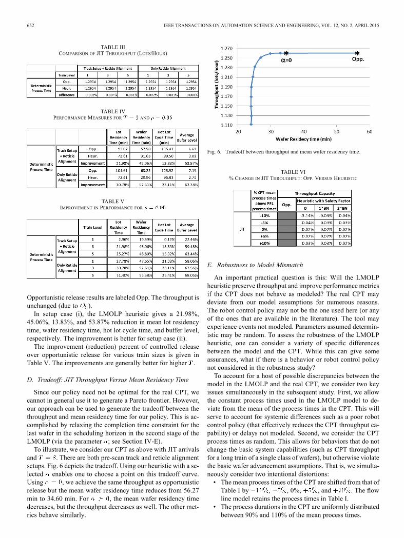
Since our policy need not be optimal for the real CPT, wecannot in general use it to generate a Pareto frontier. However,our approach can be used to generate the tradeoff between thethroughput and mean residency time for our policy. This is ac-complished by relaxing the completion time constraint for thelast wafer in the scheduling horizon in the second stage of theLMOLP (via the parameter ; see Section IV-E).To illustrate, we consider our CPT as above with JIT arrivals
and . There are both pre-scan track and reticle alignmentsetups. Fig. 6 depicts the tradeoff. Using our heuristic with a se-lected enables one to choose a point on this tradeoff curve.Using , we achieve the same throughput as opportunisticrelease but the mean wafer residency time reduces from 56.27min to 34.60 min. For , the mean wafer residency timedecreases, but the throughput decreases as well. The other met-rics behave similarly.
Fig. 6. Tradeoff between throughput and mean wafer residency time.
TABLE VI% CHANGE IN JIT THROUGHPUT: OPP. VERSUS HEURISTIC
E. Robustness to Model Mismatch
An important practical question is this: Will the LMOLPheuristic preserve throughput and improve performance metricsif the CPT does not behave as modeled? The real CPT maydeviate from our model assumptions for numerous reasons.The robot control policy may not be the one used here (or anyof the ones that are available in the literature). The tool mayexperience events not modeled. Parameters assumed determin-istic may be random. To assess the robustness of the LMOLPheuristic, one can consider a variety of specific differencesbetween the model and the CPT. While this can give someassurances, what if there is a behavior or robot control policynot considered in the robustness study?To account for a host of possible discrepancies between the
model in the LMOLP and the real CPT, we consider two keyissues simultaneously in the subsequent study. First, we allowthe constant process times used in the LMOLP model to de-viate from the mean of the process times in the CPT. This willserve to account for systemic differences such as a poor robotcontrol policy (that effectively reduces the CPT throughput ca-pability) or delays not modeled. Second, we consider the CPTprocess times as random. This allows for behaviors that do notchange the basic system capabilities (such as CPT throughputfor a long train of a single class of wafers), but otherwise violatethe basic wafer advancement assumptions. That is, we simulta-neously consider two intentional distortions:• The mean process times of the CPT are shifted from that ofTable I by , , 0%, , and . The flowline model retains the process times in Table I.
• The process durations in the CPT are uniformly distributedbetween 90% and 110% of the mean process times.

PARK AND MORRISON: CONTROLLED WAFER RELEASE IN CLUSTERED PHOTOLITHOGRAPHY TOOLS 653
TABLE VIIPERFORMANCE MEASURES FOR AND
To ensure the throughput provided by the LMOLP heuristicis robust to such discrepancies, we include a safety factor in therelease times. That is, we use , where, , and are the release time used in the CPT, release
time provide by the LMOLP heuristic, arrival time of wafer ,and safety factor, respectively.We study the CPT with and both pre-scan track and
reticle alignment setups.Table VI provides the JIT throughput (this is the capacity of
the CPT) change associated with our policy. The safety factoris stated as a multiple of the model's bottleneck process time(denoted as BN). Only when the process times of the CPT are10% faster than in the LMOLP model with zero safety factor,is there a loss of throughput ( ). However, it is reme-died with just one bottleneck safety factor. For the other cases,there is no loss of JIT throughput (only noise). Note that theCPT being faster than the flow line models is not the case ofgeneral concern. As such, for a poor robot policy or unmodeleddelays, in which the flow line model is faster than the actualCPT, the LMOLP heuristic is expected to guarantee maximumthroughput.Even though the wafers are admitted later than recommended
by the LMOLPwhen using a safety factor, the performance met-rics still improve significantly. Results with 95% loading aredepicted in Table VII. There remains at least a 14%, 27%, and10% improvement in lot residency time, wafer residency time,and hot lot cycle time, respectively.
VIII. CONCLUDING REMARKS
Opportunistic wafer release is common in practical CPTs.While it serves to guarantee throughput capability, it causes un-necessarily large wafer residency times and reduces agility.By judiciously admitting wafers, we endeavor to maintain
throughput capacity while minimizing residency time. The fullwafer release problem, including wafer handling robots, is toocomputationally complex for practical purposes. As such, wedevelop a real-time control heuristic using an LMOLP and anFFL relaxation of the detailed systemmodel. The FFLmodel in-corporates many features of real world CPTs. As the underlyingLMOLP is polynomial time, the approach is computationallyfriendly. One key caveat is that the CPT be process bound; this
is common in practice. (However, based on the robustness studyof Section VII-E, this may not be necessary.)Numerical studies using a detailed CPT model based on real
industry data from the literature were conducted. The heuristicsignificantly reduced the mean wafer residency, lot residencyand hot lot cycle times. Mean buffer levels reduced as well.There was no loss of throughput. The LMOLP heuristic provedrobust to mismatches between the CPT behavior and the flowline model used in the LMOLP.There are numerous possible future research directions. Ob-
taining CPT yield data showing a correlation between wafer res-idency time and yield would be very motivating. Developingcomputationally tractable methods to jointly schedule wafer re-leases and wafer transport robots could give some additionalresidency time reduction. While a total tool failure should behandled as it is presently, methods to address CPTs with reducedcapacity due to a single module failure could be considered. Fi-nally, it is desirable to implement the approach in an operatingCPT in a wafer fabricator.
REFERENCES[1] Global Semiconductor Forum 2011, “Elpida memory 300 mm wafer
fab,” Hiroshima, Japan, Accessed Mar. 31, 2011. [Online]. Available:http://www.semiconductor-technology.com/projects/elpida
[2] P. Marcoux, M. McClintock, D. Martin, and R. Woods, “Determiningcapacity loss from operational and technical deployment practices ina semiconductor manufacturing line,” in Proc. IEEE Int. Semicond.Manuf. Symp., 1999, pp. 3–5.
[3] S. Piramuthu, N. Raman, and M. J. Shaw, “Learning-based schedulingin a flexible manufacturing flow line,” IEEE Trans. Eng. Manag., vol.41, no. 2, pp. 72–182, May 1994.
[4] K. Srinivasan, R. Sandell, and S. Brown, “Correlation between yieldand waiting time: A quantitative study,” in Proc. IEEE/CPMT Int. Elec.Manuf. Tech. Symp., 1995, pp. 65–69.
[5] L. M.Wein, “On the relationship between yield and cycle time in semi-conductor wafer fabrication,” IEEE Trans. Semicond. Manuf., vol. 5,no. 2, pp. 156–158, May 1992.
[6] D. Meyersdorf and T. Yang, “Cycle time reduction for semiconductorwafer fabrication facilities,” in Proc. IEEE/SEMI Adv. Semicond.Manuf. Conf. Workshop, 1997, pp. 418–423.
[7] S. C. H. Lu, D. Ramaswamy, and P. R. Kumar, “Efficient schedulingpolicies to reduce mean and variance of cycle-time in semiconductormanufacturing plants,” IEEE Trans. Semicond. Manuf., vol. 7, no. 3,pp. 374–388, Apr. 1994.
[8] W.-C. Chang, M. Yu, R. Wu, C. Chen, J. Chen, C. Y. Hsieh, and C. K.Wang, “Yield improvement through cycle time and process fluctuationanalyses,” in Proc. 2001 IEEE Int. Semicond. Manuf. Symp., 2001, pp.267–270.

654 IEEE TRANSACTIONS ON AUTOMATION SCIENCE AND ENGINEERING, VOL. 12, NO. 2, APRIL 2015
[9] S. Khetan and P. Fowler, “Managing high IC yields with short cycletimes,” in GaAs IC Symp., 1995, pp. 119–123.
[10] Wittrock and J. Robert, “Scheduling heuristics for flexible flow lines,”IBM J. Res. Develop., vol. 29, no. 4, p. 401,412, Jul. 1985.
[11] T. L. Perkinson, P. K. McLarty, R. S. Gyurcsik, and R. K. Cavin, III,“Single-wafer cluster tool performance: An analysis of throughput,”IEEE Trans. Semicond. Manuf., vol. 7, no. 3, pp. 369–373, Aug. 1994.
[12] S. Venkatesh, R. Davenport, P. Foxhoven, and J. Nulman, “A steadystate throughput analysis of cluster tools: Dual-blade versus singleblade robots,” IEEE Trans. Semicond. Manuf., vol. 10, no. 4, pp.418–424, Nov. 1997.
[13] J. Yi, S. Ding, D. Song, and M. Zhang, “Steady-state throughput andscheduling analysis of multi-cluster tools: A decomposition approach,”IEEE Trans. Autom. Sci. Eng., vol. 5, no. 2, pp. 321–336, Apr. 2008.
[14] M.W. Dawande, H. N. Geismar, and S. P. Sethi, Throughput Optimiza-tion in Robotic Cells. New York, NY, USA: Springer, 2007.
[15] M. Zhou andM. Jeng, “Modeling, analysis, simulation, scheduling, andcontrol of semiconductor manufacturing: A Petri net approach,” IEEETrans. Semicond. Manuf., vol. 11, no. 3, pp. 333–357, Aug. 1998.
[16] J.-H. Kim, T.-E. Lee, H.-Y. Lee, and D.-B. Park, “Scheduling analysisof time-constrained dual-armed cluster tools,” IEEE Trans. Semicond.Manuf., vol. 16, no. 3, pp. 521–534, Aug. 2003.
[17] W. M. Zuberek, “Timed Petri nets in modeling and analysis of clustertools,” IEEE Trans. Robot. Autom., vol. 17, no. 5, pp. 562–575, Oct.2001.
[18] N. Wu, C. Chu, F. Chu, and M. C. Zhou, “A Petri net method forschedulability and scheduling problems in single-arm cluster tools withwafer residency time constraints,” IEEE Trans. Semicond. Manuf., vol.21, no. 2, pp. 224–237, May 2008.
[19] W. K. V. Chan, J. Yi, and S. Ding, “Optimal scheduling of multiclustertools with constant robot moving times, Part I: Two-cluster analysis,”IEEE Trans. Autom. Sci. Eng., vol. 8, no. 1, pp. 5–16, Jan. 2011.
[20] D. Pillai, “The future of semiconductor manufacturing: Factory inte-gration breakthrough opportunities,” IEEE Robot. Autom. Mag., vol.13, no. 4, pp. 16–24, Dec. 2006.
[21] N. Q. Wu and M. C. Zhou, “Modeling, Analysis and control ofdual-arm cluster tools with residency time constraints and activitytime variation based on Petri nets,” IEEE Trans. Autom. Sci. Eng., vol.9, no. 2, pp. 446–454, Apr. 2012.
[22] J.-H. Kim and T.-E. Lee, “Schedulability analysis of time-constrainedcluster tools with bounded time variation by an extended Petri net,”IEEE Trans. Autom. Sci. Eng., vol. 5, no. 3, p. 490,503, Jul. 2008.
[23] N. Q. Wu andM. C. Zhou, “Schedulability analysis and optimal sched-uling of dual-arm cluster tools with residency time constraints and ac-tivity time variation,” IEEE Trans. Autom. Sci. Eng., vol. 9, no. 1, pp.203–209, Jan. 2012.
[24] H. N. Geismar, C. Sriskandarajah, and N. Ramanan, “Increasingthroughput for robotic cells with parallel machines and multiplerobots,” IEEE Trans. Autom. Sci. Eng., vol. 1, no. 1, pp. 84–89, Jul.2004.
[25] M. LaPedus, “EUV tool costs hit $120 million,” EETimes, Nov. 2010.[26] D.-K. Kim and T.-E. Lee, “Cyclic scheduling of sequentially
connected cluster tools with a single I/O module,” in Proc. IFACConf. Manuf. Modelling, Manag. Control, Jun. 19–21, 2013,pp. 146–151.
[27] Q. Zhu, N. Wu, Y. Qiao, and M. C. Zhou, “Petri net modeling andone-wafer scheduling of single-arm multi-cluster tools,” in Proc. 9thIEEE Int. Conf. Autom. Sci. Eng., Aug. 17–21, 2013.
[28] J. R. Morrison, “Multiclass flow line models of semiconductor manu-facturing equipment for fab-level simulation,” IEEE Trans. Autom. Sci.Eng., vol. 8, no. 1, pp. 81–94, Jan. 2011.
[29] M.-C. Wu and C.-W. Chiou, “Scheduling semiconductor in-line scan-ners in new product/process introduction scenarios,” Int. J. Product.Res., vol. 48, no. 6, pp. 1835–1852, 2010.
[30] C.-W. Chiou and M.-C. Wu, “Scheduling of multiple in-line scannersfor semiconductor wafer fabs,” Int. J. Syst. Sci., vol. 45, no. 3, pp.384–398, Mar. 2014.
[31] A. A. A. Kock, L. F. P. Etman, and J. E. Rooda, “Lumped parametermodeling of the litho cell,” Inform. Control Probl. Manuf., vol. 12, no.1, pp. 709–714, 2006.
[32] J. R. Morrison and D. P. Martin, “Performance evaluation of pho-tolithography cluster tools: Queueing and throughput models,” ORSpectrum, vol. 11, no. 4, pp. 375–389, 2007.
[33] A. A. A. Kock, C. P. L. Veeger, L. F. P. Etman, B. Lemmen, and J. E.Rooda, “Cycle time and throughput performance analysis of a litho cellusing an aggregate modeling approach,” in Proc. the Adv. Semicond.Manuf. Conf. (ASMC), 2007, pp. 65–70.
[34] A. A. A. Kock, C. P. L. Veeger, L. F. P. Etman, B. Lemmen, and J.E. Rooda, “Lumped parameter modelling of the litho cell,” Product.Planning Control, A Special Issue on Novel Models and Approachesfor Semiconductor Manufacturing, vol. 22, no. 1, pp. 41–49, 2011.
[35] A. Schrijver, Theory of Linear and Integer Programming. New York,NY, USA: Wiley, 1998.
[36] C. H. Papadimitriou and P. C. Kanellakis, “Flowshop scheduling withlimited temporary storage,” J. Assoc. Comput. Mach., vol. 27, no. 3,pp. 533–549, 1980.
[37] F. Mahmoodi, K. J. Dooley, and P. J. Starr, “An evaluation of order re-leasing and due date assignment heuristics in a cellular manufacturingsystem,” J. Oper. Manag., vol. 9, pp. 548–573, 1990.
[38] G. L. Ragatz and V. A. Mabert, “An evaluation of order release mecha-nisms in a job-shop environment,” Decision Sci., vol. 19, pp. 167–189,1988.
[39] R.Wittrock, “An adaptable scheduling heuristic for flexible flow lines,”Oper. Res., vol. 36, no. 3, pp. 445–453, 1988.
[40] A. Agnetis, A. Pacifici, F. Rossi, M. Lucertini, S. Nicoletti, F. Nicolo,G. Oriolo, D. Pacciarelli, and E. Pesaro, “Scheduling of flexible flowlines in automobile assembly plant,” Eur. J. Oper. Res., vol. 97, pp.348–362, 1997.
[41] T. Sawik, “An exact approach for batch scheduling in flexible flow lineswith limited intermediate buffers,” Math. Comput. Modeling, vol. 36,pp. 461–471, 2002.
[42] T. Sawik, A. Schaller, and T. M. Tirpak, “Scheduling of printed wiringboard assembly in surface mount technology lines,” Product. Plan-ning and Scheduling in Electron. Manuf., Special Issue on J. Electron.Manuf., vol. 11, no. 1, pp. 1–17, 2002.
[43] G. Sullivan, “Logistics management system (LMS): Integrating de-cision technologies for dispatch scheduling in semiconductor manu-facturing,” in Intell. Scheduling, M. Fox and M. Zweben, Eds. SanMateo, CA, USA: Morgan Kaufman, 1994, ch. 17, pp. 473–516.
[44] R. A. Bowman, “Job release control using a cyclic schedule,” Prod.Operat. Manag., vol. 11, no. 11, pp. 274–287, 2002.
[45] L. M. Wein, “Scheduling semiconductor wafer fabrication,” IEEETrans. Semicond. Manuf., vol. 1, no. 3, pp. 115–130, Aug. 1988.
[46] J. W. M. Bertrand, J. P. Brans, Ed., “The effect of workload control onorder flow times,” in Proc. Oper Res., 1981, pp. 779–789.
[47] S. C. Sarin, M. P. Greco, and E. M. Dar-El, “Sequencing and loadingof products on a flow line,” Eur. J. Oper. Res., vol. 168, no. 3, pp.905–921, 2006.
[48] S. T. McCormick, M. L. Pinedo, S. Shenker, and B.Wolf, “Sequencingin an assembly line with blocking to minimize cycle time,” Oper. Res.,vol. 37, no. 6, pp. 925–935, 1989.
[49] W. K. V. Chan and L. W. Schruben, “Optimization models of discrete-event system dynamics,” Oper. Res., vol. 56, pp. 1218–1237, 2008.
[50] K. Park and J. R. Morrison, “Control of wafer release in multi clustertools,” in Proc. 8th IEEE Int. Conf. Control Autom. (ICCA), Jun. 2010,pp. 1481–1487.
[51] K. Park and J. R. Morrison, “Wafer admission control for clusteredphotolithography tools,” in Proc. IEEE/SEMI Adv. Semicond. Manuf.Conf. (ASMC), Jul. 2010, pp. 220–225.
[52] K. Park and J. R. Morrison, “Scheduling wafer release in clusteredphotolithography tools,” in Proc. 5th Multidisciplinary Int. SchedulingConf. (MISTA'11), Aug. 2011, pp. 639–641.
[53] H. J. Yoon and D. Y. Lee, “Deadlock-free scheduling of photolithog-raphy equipment in semiconductor fabrication,” IEEE Trans. Semi-cond. Manuf., vol. 17, no. 1, pp. 42–54, Feb. 2004.
[54] N. Wu and M. C. Zhou, “Real-time deadlock scheduling for semicon-ductor track systems based on colored timed Petri nets,” OR Spectrum,vol. 29, no. 3, pp. 421–433, 2007.
[55] N. Wu and M. C. Zhou, “Deadlock modeling and control of semicon-ductor track systems using resource-oriented Petri nets,” Int. J. Prod.Res., vol. 45, no. 15, pp. 3439–3456, 2007.
[56] U. Wikborg and T.-E. Lee, “Noncyclic scheduling for timed dis-crete-event systems with application to single-armed cluster toolsusing Pareto-optimal optimization,” IEEE Trans. Autom. Sci. Eng.,vol. 10, no. 3, pp. 699–710, Jul. 2013.
[57] N. Q. Wu, F. Chu, C. B. Chu, and M. C. Zhou, “Petri net-based sched-uling of single-arm cluster tools with reentrant atomic layer depositionprocesses,” IEEE Trans. Autom. Sci. Eng., vol. 8, no. 1, pp. 42–55,2011.
[58] N. Q. Wu and M. C. Zhou, System Modeling and Control With Re-source-Oriented Petri Nets. Boca Raton, FL, USA: CRC Press, 2010.
[59] L. Li, Z. Sun, M. C. Zhou, and F. Qiao, “Adaptive dispatching rulefor semiconductor wafer fabrication facility,” IEEE Trans. Autom. Sci.Eng., vol. 10, no. 2, pp. 353–464, Apr. 2013.

PARK AND MORRISON: CONTROLLED WAFER RELEASE IN CLUSTERED PHOTOLITHOGRAPHY TOOLS 655
[60] H.-J. Kim, J.-H. Lee, and T.-E. Lee, “Scheduling cluster tools withready time constraints for consecutive small lots,” IEEE Trans. Autom.Sci. Eng., vol. 10, no. 1, pp. 145–159, Jan. 2013.
[61] W. K. Chan, J. G. Yi, S. W. Ding, and D. Z. Song, “Optimal schedulingof multi-cluster tools with constant robot moving times, Part II: Tree-like topology configurations,” IEEE Trans. Autom. Sci. Eng., vol. 8, no.1, pp. 17–28, Jan. 2011.
[62] Y. Qiao, N. Q. Wu, and M. C. Zhou, “Real-time scheduling ofsingle-arm cluster tools subject to residency time constraints andbounded activity time variation,” IIEEE Trans. Autom. Sci. Eng., vol.9, no. 3, pp. 564–577, Jul. 2012.
[63] N. Q. Wu and M. C. Zhou, “A closed-form solution for schedula-bility and optimal scheduling of dual-arm cluster tools with wafer resi-dency time constraint based on steady schedule analysis,” IEEE Trans.Autom. Sci. Eng., vol. 7, no. 2, pp. 303–315, Apr. 2010.
[64] B. Avi-Itzhak, “A sequence of service stations with arbitrary input andregular service times,” Manag. Sci., vol. 11, no. 5, pp. 565–571, 1965.
[65] J. P. Ignizio, Goal Programming and Extensions. Lanham, MD,USA: Lexington Books, 1976.
[66] J. P. Ignizio and L. C. Thomas, “An enhanced conversion scheme forlexicographic, multiobjective integer programs,” Eur. J. Oper. Res.,vol. 18, no. 1, pp. 57–61, 1984.
[67] D. G. Luenberger and Y. Ye, Linear and Nonlinear Programming.New York, NY, USA: Springer, 2008.
[68] K. Park, “Flow line models for high-tech manufacturing: Theory, ap-plication and optimization,” Ph.D. dissertation, Daejeon, Korea, Feb.2014.
[69] S. Kumar, N. Ramanan, and C. Sriskandarajah, “Minimizing cycle timein large robotic cells,” IIE Trans., vol. 37, no. 2, pp. 123–136, Feb.2005.
[70] “Tokyo Electron Limited Completes Acquisition of FSI International,Inc.” Tokyo Electron News Website Public Relations Group, TokyoElectron Ltd., Oct. 12, 2012. [Online]. Available: http://www.tel.com/news/2012/1012_001.htm
Kyungsu Park received the B.S. degree in informa-tion and industrial engineering and the B.S. degreein chemical engineering from Yonsei University,Yonsei, Korea, in 2008, and the Ph.D. degree fromthe Department of Industrial and Systems Engi-neering, Korea Advanced Institute of Science andTechnology, Daejeon, Korea, in 2014.He is currently a Senior Researcher with the De-
fense Agency for Technology andQuality, Korea. Hisresearch interest is on modeling and scheduling insemiconductor manufacturing.
James R. Morrison (S'97–M'00) received the B.S.degree in electrical engineering and the B.S. degree inmathematics from the University of Maryland, Col-lege Park, MD, USA, the M.S. and Ph.D. degrees inelectrical and computer engineering from the Uni-versity of Illinois at Urbana–Champaign, Urbana, IL,USA, in 1997 and 2000, respectively.He was with the Fab Operations Engineering De-
partment, IBM Corporation from 2000 to 2005. Heis currently an Associate Professor with the Depart-ment of Industrial and Systems Engineering, KAIST,
Korea. His research interests include semiconductor wafer fabrication, roboticservice agents, design of services and eco-design.Prof. Morrison has served as the corresponding Co-Chair of the IEEE
Robotics and Automation Society Technical Committee on SemiconductorManufacturing Automation since January 2009.