68-pin shielded connector block - national instruments · daq ni scb-68a user manual 68-pin...
TRANSCRIPT

DAQNI SCB-68A User Manual68-Pin Shielded Connector Block
NI SCB-68A User Manual
ni.com/manuals
DeutschFrançais
August 2012375865A-01

Support
Worldwide Technical Support and Product Informationni.com
Worldwide Offices
Visit ni.com/niglobal to access the branch office Web sites, which provide up-to-date contact information, support phone numbers, email addresses, and current events.
National Instruments Corporate Headquarters
11500 North Mopac Expressway Austin, Texas 78759-3504 USA Tel: 512 683 0100
For further support information, refer to the Technical Support and Professional Services appendix. To comment on National Instruments documentation, refer to the National Instruments Web site at ni.com/info and enter the Info Code feedback.
© 2012 National Instruments. All rights reserved.

Important Information
WarrantyThe SCB-68A is warranted against defects in materials and workmanship for a period of one year from the date of shipment, as evidenced by receipts or other documentation. National Instruments will, at its option, repair or replace equipment that proves to be defective during the warranty period. This warranty includes parts and labor.
The media on which you receive National Instruments software are warranted not to fail to execute programming instructions, due to defects in materials and workmanship, for a period of 90 days from date of shipment, as evidenced by receipts or other documentation. National Instruments will, at its option, repair or replace software media that do not execute programming instructions if National Instruments receives notice of such defects during the warranty period. National Instruments does not warrant that the operation of the software shall be uninterrupted or error free.
A Return Material Authorization (RMA) number must be obtained from the factory and clearly marked on the outside of the package before any equipment will be accepted for warranty work. National Instruments will pay the shipping costs of returning to the owner parts which are covered by warranty.
National Instruments believes that the information in this document is accurate. The document has been carefully reviewed for technical accuracy. In the event that technical or typographical errors exist, National Instruments reserves the right to make changes to subsequent editions of this document without prior notice to holders of this edition. The reader should consult National Instruments if errors are suspected. In no event shall National Instruments be liable for any damages arising out of or related to this document or the information contained in it.
EXCEPT AS SPECIFIED HEREIN, NATIONAL INSTRUMENTS MAKES NO WARRANTIES, EXPRESS OR IMPLIED, AND SPECIFICALLY DISCLAIMS ANY WARRANTY OF MERCHANTABILITY OR FITNESS FOR A PARTICULAR PURPOSE. CUSTOMER’S RIGHT TO RECOVER DAMAGES CAUSED BY FAULT OR NEGLIGENCE ON THE PART OF NATIONAL INSTRUMENTS SHALL BE LIMITED TO THE AMOUNT THERETOFORE PAID BY THE CUSTOMER. NATIONAL INSTRUMENTS WILL NOT BE LIABLE FOR DAMAGES RESULTING FROM LOSS OF DATA, PROFITS, USE OF PRODUCTS, OR INCIDENTAL OR CONSEQUENTIAL DAMAGES, EVEN IF ADVISED OF THE POSSIBILITY THEREOF. This limitation of the liability of National Instruments will apply regardless of the form of action, whether in contract or tort, including negligence. Any action against National Instruments must be brought within one year after the cause of action accrues. National Instruments shall not be liable for any delay in performance due to causes beyond its reasonable control. The warranty provided herein does not cover damages, defects, malfunctions, or service failures caused by owner’s failure to follow the National Instruments installation, operation, or maintenance instructions; owner’s modification of the product; owner’s abuse, misuse, or negligent acts; and power failure or surges, fire, flood, accident, actions of third parties, or other events outside reasonable control.
CopyrightUnder the copyright laws, this publication may not be reproduced or transmitted in any form, electronic or mechanical, including photocopying, recording, storing in an information retrieval system, or translating, in whole or in part, without the prior written consent of National Instruments Corporation.
National Instruments respects the intellectual property of others, and we ask our users to do the same. NI software is protected by copyright and other intellectual property laws. Where NI software may be used to reproduce software or other materials belonging to others, you may use NI software only to reproduce materials that you may reproduce in accordance with the terms of any applicable license or other legal restriction.
End-User License Agreements and Third-Party Legal NoticesYou can find end-user license agreements (EULAs) and third-party legal notices in the following locations:
• Notices are located in the <National Instruments>\_Legal Information and <National Instruments> directories.
• EULAs are located in the <National Instruments>\Shared\MDF\Legal\license directory.
• Review <National Instruments>\_Legal Information.txt for more information on including legal information in installers built with NI products.
TrademarksLabVIEW, National Instruments, NI, ni.com, the National Instruments corporate logo, and the Eagle logo are trademarks of National Instruments Corporation. Refer to the Trademark Information at ni.com/trademarks for other National Instruments trademarks.
Taptite and Trilobular are registered trademarks of Research Engineering & Manufacturing Inc. Other product and company names mentioned herein are trademarks or trade names of their respective companies.
Members of the National Instruments Alliance Partner Program are business entities independent from National Instruments and have no agency, partnership, or joint-venture relationship with National Instruments.
PatentsFor patents covering National Instruments products/technology, refer to the appropriate location: Help»Patents in your software, the patents.txt file on your media, or the National Instruments Patent Notice at ni.com/patents.
Export Compliance InformationRefer to the Export Compliance Information at ni.com/legal/export-compliance for the National Instruments global trade compliance policy and how to obtain relevant HTS codes, ECCNs, and other import/export data.
WARNING REGARDING USE OF NATIONAL INSTRUMENTS PRODUCTS(1) NATIONAL INSTRUMENTS PRODUCTS ARE NOT DESIGNED WITH COMPONENTS AND TESTING FOR A LEVEL OF RELIABILITY SUITABLE FOR USE IN OR IN CONNECTION WITH SURGICAL IMPLANTS OR AS CRITICAL COMPONENTS IN ANY LIFE SUPPORT SYSTEMS WHOSE FAILURE TO PERFORM CAN REASONABLY BE EXPECTED TO CAUSE SIGNIFICANT INJURY TO A HUMAN.

(2) IN ANY APPLICATION, INCLUDING THE ABOVE, RELIABILITY OF OPERATION OF THE SOFTWARE PRODUCTS CAN BE IMPAIRED BY ADVERSE FACTORS, INCLUDING BUT NOT LIMITED TO FLUCTUATIONS IN ELECTRICAL POWER SUPPLY, COMPUTER HARDWARE MALFUNCTIONS, COMPUTER OPERATING SYSTEM SOFTWARE FITNESS, FITNESS OF COMPILERS AND DEVELOPMENT SOFTWARE USED TO DEVELOP AN APPLICATION, INSTALLATION ERRORS, SOFTWARE AND HARDWARE COMPATIBILITY PROBLEMS, MALFUNCTIONS OR FAILURES OF ELECTRONIC MONITORING OR CONTROL DEVICES, TRANSIENT FAILURES OF ELECTRONIC SYSTEMS (HARDWARE AND/OR SOFTWARE), UNANTICIPATED USES OR MISUSES, OR ERRORS ON THE PART OF THE USER OR APPLICATIONS DESIGNER (ADVERSE FACTORS SUCH AS THESE ARE HEREAFTER COLLECTIVELY TERMED “SYSTEM FAILURES”). ANY APPLICATION WHERE A SYSTEM FAILURE WOULD CREATE A RISK OF HARM TO PROPERTY OR PERSONS (INCLUDING THE RISK OF BODILY INJURY AND DEATH) SHOULD NOT BE RELIANT SOLELY UPON ONE FORM OF ELECTRONIC SYSTEM DUE TO THE RISK OF SYSTEM FAILURE. TO AVOID DAMAGE, INJURY, OR DEATH, THE USER OR APPLICATION DESIGNER MUST TAKE REASONABLY PRUDENT STEPS TO PROTECT AGAINST SYSTEM FAILURES, INCLUDING BUT NOT LIMITED TO BACK-UP OR SHUT DOWN MECHANISMS. BECAUSE EACH END-USER SYSTEM IS CUSTOMIZED AND DIFFERS FROM NATIONAL INSTRUMENTS' TESTING PLATFORMS AND BECAUSE A USER OR APPLICATION DESIGNER MAY USE NATIONAL INSTRUMENTS PRODUCTS IN COMBINATION WITH OTHER PRODUCTS IN A MANNER NOT EVALUATED OR CONTEMPLATED BY NATIONAL INSTRUMENTS, THE USER OR APPLICATION DESIGNER IS ULTIMATELY RESPONSIBLE FOR VERIFYING AND VALIDATING THE SUITABILITY OF NATIONAL INSTRUMENTS PRODUCTS WHENEVER NATIONAL INSTRUMENTS PRODUCTS ARE INCORPORATED IN A SYSTEM OR APPLICATION, INCLUDING, WITHOUT LIMITATION, THE APPROPRIATE DESIGN, PROCESS AND SAFETY LEVEL OF SUCH SYSTEM OR APPLICATION.

Conventions
The following conventions are used in this manual:
<> Angle brackets that contain numbers separated by an ellipsis represent a range of values associated with a bit or signal name—for example, AO <3..0>.
» The » symbol leads you through nested menu items and dialog box options to a final action. The sequence Options»Settings»General directs you to pull down the Options menu, select the Settings item, and select General from the last dialog box.
This icon denotes a tip, which alerts you to advisory information.
This icon denotes a note, which alerts you to important information.
This icon denotes a caution, which advises you of precautions to take to avoid injury, data loss, or a system crash. When this symbol is marked on a product, refer to the Read Me First: Safety and Electromagnetic Compatibility document for information about precautions to take.
bold Bold text denotes items that you must select or click in the software, such as menu items and dialog box options. Bold text also denotes parameter names.
italic Italic text denotes variables, emphasis, a cross-reference, or an introduction to a key concept. Italic text also denotes text that is a placeholder for a word or value that you must supply.
monospace Text in this font denotes text or characters that you should enter from the keyboard, sections of code, programming examples, and syntax examples. This font is also used for the proper names of disk drives, paths, directories, programs, subprograms, subroutines, device names, functions, operations, variables, filenames, and extensions.
© National Instruments | vii
Contents
Chapter 1Getting Started with the SCB-68AWhat You Need to Get Started ......................................................................................... 1-2Setting up the SCB-68A ................................................................................................... 1-3Using the SCB-68A in Direct Feedthrough Mode ........................................................... 1-6Using the SCB-68A with MIO DAQ Devices.................................................................. 1-7Mounting the SCB-68A.................................................................................................... 1-9
Panel Mounting......................................................................................................... 1-9DIN Rail Mounting................................................................................................... 1-10
Securing the Cover on the SCB-68A................................................................................ 1-11Soldering and Desoldering Components on the SCB-68A .............................................. 1-11
Soldering Equipment ................................................................................................ 1-11Removing the SCB-68A Board from the Base......................................................... 1-11Soldering and Desoldering Guidelines ..................................................................... 1-12
Related Documentation .................................................................................................... 1-13
Chapter 2Analog Input and Temperature Sensor MeasurementsAnalog Input Circuitry and Channel Pad Configuration .................................................. 2-2Connecting Analog Input Signals..................................................................................... 2-5
Floating Signal Sources ............................................................................................ 2-7When to Use Differential Connections with Floating Signal Sources ............. 2-7When to Use Non-Referenced Single-Ended (NRSE) Connections with
Floating Signal Sources................................................................................. 2-7When to Use Referenced Single-Ended (RSE) Connections with
Floating Signal Sources................................................................................. 2-8Using Differential Connections for Floating Signal Sources ........................... 2-8Using Non-Referenced Single-Ended (NRSE) Connections for
Floating Signal Sources................................................................................. 2-11Using Referenced Single-Ended (RSE) Connections for
Floating Signal Sources................................................................................. 2-12Ground-Referenced Signal Sources.......................................................................... 2-12
When to Use Differential Connections with Ground-Referenced Signal Sources .............................................................. 2-12
When to Use Non-Referenced Single-Ended (NRSE) Connections with Ground-Referenced Signal Sources .............................................................. 2-13
When to Use Referenced Single-Ended (RSE) Connections with Ground-Referenced Signal Sources .............................................................. 2-13
Using Differential Connections for Ground-Referenced Signal Sources......... 2-14Using Non-Referenced Single-Ended (NRSE) Connections for
Ground-Referenced Signal Sources .............................................................. 2-15

Contents
viii | ni.com
Using the Temperature Sensor..........................................................................................2-16Taking Thermocouple Measurements ......................................................................2-16Temperature Sensor Output and Accuracy...............................................................2-17Thermocouple Sources of Error................................................................................2-17Open Thermocouple Detection .................................................................................2-18Thermocouple Input Filtering...................................................................................2-19
Installing Bias Resistors....................................................................................................2-20Lowpass Filtering .............................................................................................................2-21
One-Pole Lowpass RC Filter ....................................................................................2-24Selecting Components for Lowpass Filtering...........................................................2-24Adding Components for Lowpass Filters on Analog Input Signals .........................2-25Analog Input Lowpass Filtering Applications..........................................................2-26
Highpass Filtering.............................................................................................................2-27One-Pole Highpass RC Filter ...................................................................................2-29Selecting Components for Highpass Filtering ..........................................................2-29Adding Components for Highpass Filtering on Analog Input Signals .....................2-30Analog Input Highpass Filtering Applications .........................................................2-31
Current Input Measurement ..............................................................................................2-32Selecting a Resistor for Current Input Measurement................................................2-33Adding Components for Current Input Measurement on Analog Input Signals ......2-33
Attenuating Voltage ..........................................................................................................2-35Selecting Components for Attenuating Voltage .......................................................2-36Accuracy Considerations for Attenuating Voltage ...................................................2-36Adding Components for Attenuating Voltage on Analog Input Signals ..................2-37Analog Input Voltage Dividers.................................................................................2-38
Chapter 3Analog Output WaveformsAnalog Output Channel Pad Configuration......................................................................3-1Lowpass Filtering .............................................................................................................3-2
One-Pole Lowpass RC Filter ....................................................................................3-5Selecting Components for Lowpass Filtering...........................................................3-6Adding Components for Lowpass Smoothing Filters on Analog Output Signals ....3-6Analog Output Lowpass Filtering Applications .......................................................3-7
Attenuating Voltage ..........................................................................................................3-8Selecting Components for Attenuating Voltage .......................................................3-9Accuracy Considerations for Attenuating Voltage ...................................................3-9Adding Components for Attenuating Voltage on Analog Output Signals ...............3-9Analog Output Voltage Dividers ..............................................................................3-10

NI SCB-68A User Manual
© National Instruments | ix
Chapter 4PFI 0 and Digital Input MeasurementsPFI 0 Channel Pad Configuration..................................................................................... 4-1Lowpass Filtering ............................................................................................................. 4-2
One-Pole Lowpass RC Filter .................................................................................... 4-5Selecting Components for Lowpass Filtering .......................................................... 4-5Adding Components for Lowpass Digital Filtering on
Digital Trigger Input Signals................................................................................. 4-6PFI 0 Lowpass Filtering Applications ...................................................................... 4-7
Attenuating Voltage.......................................................................................................... 4-8Selecting Components for Attenuating Voltage....................................................... 4-9Accuracy Considerations for Attenuating Voltage................................................... 4-9Adding Components for Attenuating Voltage on Digital Inputs.............................. 4-9Digital Input Voltage Dividers ................................................................................. 4-10
Chapter 5Fuse and Power InformationPower Supply Circuitry .................................................................................................... 5-1Fuse................................................................................................................................... 5-1Adding Power Filters........................................................................................................ 5-2
Appendix ASpecifications
Appendix BTechnical Support and Professional Services
© National Instruments | 1-1
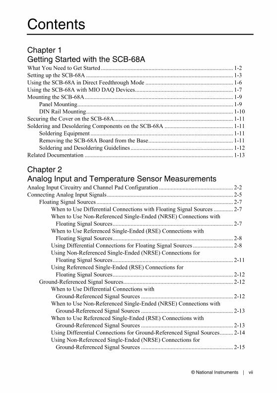
1Getting Started with the SCB-68A
The SCB-68A, shown in Figure 1-1, is a shielded I/O connector block with 68 screw terminals for easy signal connection to a National Instruments 68-pin or 100-pin DAQ device.
Figure 1-1. SCB-68A Parts Locator Diagram
The SCB-68A features a general breadboard area for custom circuitry and through hole pads for interchanging electrical components. These through hole pads allow filtering, 4 to 20 mA
1 Top Cover (Required)2 Quick Reference Label3 Enclosure Base
4 Strain-Relief Screws5 Strain-Relief Bar6 SCB-68A Board Assembly
4
5
4
1
2
3
6

1-2 | ni.com
Chapter 1 Getting Started with the SCB-68A
current input measurement, open thermocouple detection, and voltage attenuation. The open component pads allow you to easily add signal conditioning to the analog input (AI), analog output (AO), and PFI 0 signals of a 68-pin or 100-pin DAQ device.
This chapter describes how to connect and use the NI SCB-68A with 68-pin or 100-pin data acquisition (DAQ) devices and other NI products with a 68-pin SCSI or VHDCI I/O connector. For a complete list of supported devices and available SCB-68A features, refer to the KnowledgeBase document, Compatible Devices and Cabling for the NI SCB-68/SCB-68A Terminal Block. To access this document, go to ni.com/info and enter the Info Code scb68Acables.
Note To use the SCB-68A with devices without analog input functionality, as well as R Series, AO Series, and DIO/TIO Series devices, you must use direct feedthrough mode, you must change the default switch setting. Refer to the Using the SCB-68A in Direct Feedthrough Mode section for more information.
What You Need to Get StartedTo set up and use your SCB-68A, you need the following:
SCB-68A 68-pin shielded connector block kit(s)1, containing the SCB-68A and SCB-68A Quick Start
Compatible 68-pin or 100-pin DAQ device, and device documentation
The correct cable(s) for your device, as listed in the KnowledgeBase document, Compatible Devices and Cabling for the NI SCB-68/SCB-68A Terminal Block. To access this document, go to ni.com/info and enter the Info Code scb68acables.
For those not using M/X Series Connector 0, the correct quick reference label or PDF for your device, which you can find in the KnowledgeBase document, Where Can I Find NI SCB-68A Quick Reference Labels?. To access this KnowledgeBase, go to ni.com/info and enter the Info Code scb68alabels.
#2 Phillips screwdriver
0.125 in. flathead screwdriver
14–30 AWG wire
Wire cutters
Wire insulation stripper
1 You can use up to two SCB-68A accessories with AO/M/X Series devices with two connectors and E Series 100-pin devices. You can use up to four SCB-68A accessories with R Series devices with four connectors, and up to three SCB-68A accessories with R Series devices with three connectors.

© National Instruments | 1-3
NI SCB-68A User Manual
Setting up the SCB-68AThe following cautions contain important safety information concerning hazardous voltages and connector blocks.
Safety Cautions Do not connect hazardous voltages (>30 Vrms/42 Vpk/60 VDC). Refer to your device documentation for information about the electrical limits of your device.
Install cover prior to use. To avoid electrical shock, do not remove SCB-68A covers unless you are qualified to do so. Before removing the cover, disconnect any live circuit from the connector block. Replace cover for use.
The chassis ground lug on your SCB-68A is for grounding high-impedance sources, such as a floating source (1 mA maximum). Do not use the chassis ground lug as a safety earth ground.
EMC Caution To ensure the specified EMC performance, operate this product only with shielded cables.
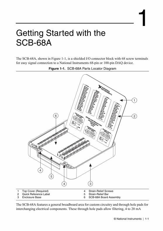
Figure 1-2 shows the SCB-68A PCB parts locator diagram.
1-4 | ni.com
Chapter 1 Getting Started with the SCB-68A
Figure 1-2. SCB-68A Printed Circuit Board Diagram
Note If the kit is missing any of the components in Figure 1-2, contact NI.
To get started with the SCB-68A, complete the following steps while referring to Figures 1-1 and 1-2. If you have not already installed your DAQ device, refer to the installation guide that came with your DAQ device for instructions. Remove all cables from the SCB-68A before getting started.
1 Temperature Sensor2 Switches S1.1 and S1.23 Analog Input Pads4 68-Pin I/O Connector5 Breadboard Area6 1 A Self-Resetting Fuse7 +5 V Power Pads, R20 and R21
8 Switches S2.1, S2.2, and S2.39 Screw Terminals10 Printed Circuit Board Mount Screw11 PFI 0 Pads12 Analog Output Pads13 Printed Circuit Board Mount Screw and Chassis Ground Lug
CAUTION: SEE MANUAL FOR ELECTRICAL RATINGSCAUTION: INSTALL COVER PRIOR TO USE
COPYRIGHT 2012©S/N 153721B-01L
FOR PATENTS:NI.COM/PATENTS
1
35
2
36
3
37
4
38
5
39
6
7
41
8
42
9
43
40
1 2 3
ON CTS
68
34
67
33
66
32
65
31
64
30
63
29
62
28
61
27
60
26
SCB-68A
S1S2
E
SC5
SC4
SC3
SC2
E
SC1
E
SC0
51
17
50
16
49
15
48
14
47
13
46
45
11
44
10
12
59
25
58
24
57
23
56
22
55
21
54
53
19
52
18
20
SC10
SC7
SC6
SC8
SC9
12
1 2 3
J5J6
J8 J4
A
FG
B
C DA
FG
B
C
A
FG
B
C
+
+
+
+
+
+
+
+
+
–
–
–
E
A
FG
B
C
+
+
+
–
E
A
FG
B
C D
+
+
+
–
E
A
FG
B
C D
+
+
+
–
118 16
116 1
181
J1F1C6
C4
R21 C2C1++
R20
C3U1
C5R38
AB
E
CD
FG+
+
+
–
+
+E
+
–
B
D
A
C
A
A
B
B
+
+
1 2 3 5 94
13 10
8
9 3
5 9 912 11
76
© National Instruments | 1-5
NI SCB-68A User Manual
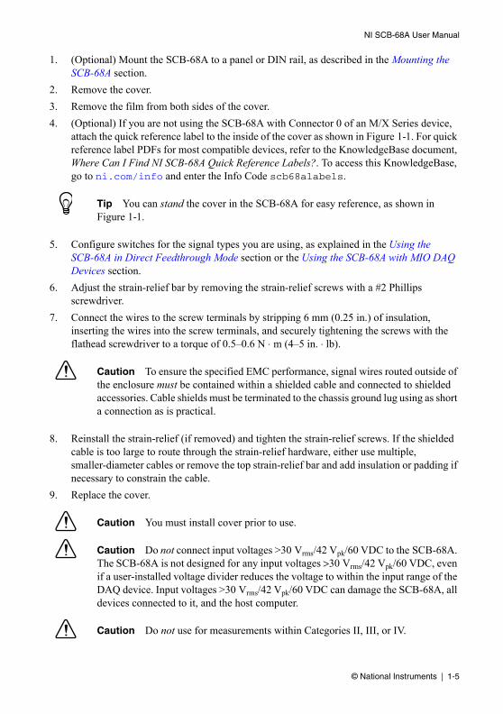
1. (Optional) Mount the SCB-68A to a panel or DIN rail, as described in the Mounting the SCB-68A section.
2. Remove the cover.
3. Remove the film from both sides of the cover.
4. (Optional) If you are not using the SCB-68A with Connector 0 of an M/X Series device, attach the quick reference label to the inside of the cover as shown in Figure 1-1. For quick reference label PDFs for most compatible devices, refer to the KnowledgeBase document, Where Can I Find NI SCB-68A Quick Reference Labels?. To access this KnowledgeBase, go to ni.com/info and enter the Info Code scb68alabels.
Tip You can stand the cover in the SCB-68A for easy reference, as shown in Figure 1-1.
5. Configure switches for the signal types you are using, as explained in the Using the SCB-68A in Direct Feedthrough Mode section or the Using the SCB-68A with MIO DAQ Devices section.
6. Adjust the strain-relief bar by removing the strain-relief screws with a #2 Phillips screwdriver.
7. Connect the wires to the screw terminals by stripping 6 mm (0.25 in.) of insulation, inserting the wires into the screw terminals, and securely tightening the screws with the flathead screwdriver to a torque of 0.5–0.6 N ⋅ m (4–5 in. ⋅ lb).
Caution To ensure the specified EMC performance, signal wires routed outside of the enclosure must be contained within a shielded cable and connected to shielded accessories. Cable shields must be terminated to the chassis ground lug using as short a connection as is practical.
8. Reinstall the strain-relief (if removed) and tighten the strain-relief screws. If the shielded cable is too large to route through the strain-relief hardware, either use multiple, smaller-diameter cables or remove the top strain-relief bar and add insulation or padding if necessary to constrain the cable.
9. Replace the cover.
Caution You must install cover prior to use.
Caution Do not connect input voltages >30 Vrms/42 Vpk/60 VDC to the SCB-68A. The SCB-68A is not designed for any input voltages >30 Vrms/42 Vpk/60 VDC, even if a user-installed voltage divider reduces the voltage to within the input range of the DAQ device. Input voltages >30 Vrms/42 Vpk/60 VDC can damage the SCB-68A, all devices connected to it, and the host computer.
Caution Do not use for measurements within Categories II, III, or IV.

1-6 | ni.com
Chapter 1 Getting Started with the SCB-68A
10. Connect the SCB-68A(s) to the DAQ device using the appropriate cable(s) for your device. For a complete list of cabling options for supported devices, refer to the KnowledgeBase document, Compatible Devices and Cabling for the NI SCB-68/SCB-68A Terminal Block. To access this document, go to ni.com/info and enter the Info Code scb68acables.
11. Launch Measurement & Automation Explorer (MAX), in the left panel, expand Devices and Interfaces to confirm that your DAQ device is recognized, and then configure your device settings.
12. (Optional) To take measurements with an MIO DAQ device, configure the SCB-68A as an accessory for a DAQ device by completing the following steps.
a. In MAX, right-click your DAQ device and select Configure.
b. On the Accessory tab, select SCB-68A from the pull-down menu and select Configure.1
c. In the Accessory Configuration window, enable or disable the temperature reference sensor and click OK.
d. Click OK.
For more information about configuring the SCB-68A for a DAQ device, refer to the Measurement & Automation Explorer Help for NI-DAQmx.
13. Test specific device functionality. Run a Test Panel in MAX by right-clicking your DAQ device and selecting Test Panels. Click Start to test the device functions.
When you have finished using the SCB-68A, power off any external signals connected to the SCB-68A before you power off your computer.
Using the SCB-68A in Direct Feedthrough ModeDevices without analog input functionality, as well as R Series, AO Series, and DIO/TIO Series devices, must use direct feedthrough mode. Move the switches to the direct feedthrough mode switch setting shown in Table 1-1.
1 MAX 5.3 or later. You can select SCB-68 as your accessory in earlier versions of MAX.
Table 1-1. Direct Feedthrough Switch Setting
Switch Setting Description
Direct feedthrough mode—Move switches S1.1, S1.2, S2.1, S2.2, and S2.3 to the positions shown at left. In this mode:
• All 68 signals from the device connect directly to screw terminals.
Refer to Figure 1-3 for a detailed diagram.
1 2 3
1
2S1 S2

© National Instruments | 1-7
NI SCB-68A User Manual
Figure 1-3. Direct Feedthrough Mode Switch Setting
Using the SCB-68A with MIO DAQ DevicesYou can take measurements with the SCB-68A and multifunction I/O (MIO) DAQ devices, such as E/M/S/X Series devices, in a number of ways. The SCB-68A has a temperature sensor for cold-junction compensation (CJC) to accommodate thermocouples; switches S1.1 and S1.2 configure the temperature sensor for different analog input settings. Switches S2.1, S2.2, and S2.3 provide power to the signal conditioning area of the accessory. Table 1-2 shows the different switch settings for MIO DAQ devices.
TemperatureSensor
Device Cable SCB-68A ScrewTerminal
68
67
1
68
67
1
22
NC
Refer to Your Device Documentationfor Device SignalInformation
SignalConditioning
NC
1 2 3
1
2S1 S2

1-8 | ni.com
Chapter 1 Getting Started with the SCB-68A
Table 1-2. MIO DAQ Device Switch Settings
Switch Setting Description
MIO with disabled temperature sensor mode (default configuration)*—Move switches S1.1, S1.2, S2.1, S2.2, and S2.3 to the positions shown at left. In this mode:
• The temperature sensor is not used.• AI 0 and AI 8 are available on screw terminals.• +5 V power provided to signal conditioning area of the
accessory.
Refer to Figure 1-4 for a detailed diagram.
MIO with single-ended temperature sensor mode*,†—Move switches S1.1, S1.2, S2.1, S2.2, and S2.3 to the positions shown at left. In this mode:
• The temperature sensor can be read using AI 0 in referenced single-ended (RSE) mode.
• AI 8 is available on a screw terminal.• +5 V power provided to signal conditioning area of the
accessory.
Refer to Figure 1-4 for a detailed diagram.
MIO with differential temperature sensor mode*—Move switches S1.1, S1.2, S2.1, S2.2, and S2.3 to the positions shown at left. In this mode:
• The temperature sensor can be read using AI 0 and AI 8 in differential mode.
• +5 V power provided to signal conditioning area of the accessory.
Refer to Figure 1-4 for a detailed diagram.
Direct feedthrough mode—Move switches S1.1, S1.2, S2.1, S2.2, and S2.3 to the positions shown at left. In this mode:
• All 68 signals from the device connect directly to screw terminals.
Refer to Figure 1-3 for a detailed diagram.
* Not available on Connector 1 of NI 6225/6255 devices.† Not available on S Series and Simultaneous MIO X Series devices.
1 2 3
1
2S1 S2
1 2 3
1
2S1 S2
1 2 3
1
2S1 S2
1 2 3
1
2S1 S2

© National Instruments | 1-9
NI SCB-68A User Manual
Figure 1-4. MIO DAQ Device Modes Switch Settings
For detailed information about connections from floating or ground-referenced signal sources to analog inputs, refer to the Connecting Analog Input Signals section of Chapter 2, Analog Input and Temperature Sensor Measurements.
Mounting the SCB-68AYou can use the SCB-68A on a desktop, or mount it to a panel or a standard DIN rail.
Panel MountingThree keyholes are located on the back of the SCB-68A for mounting it to a panel or wall. To mount the SCB-68A to a board or panel, complete the following steps.
1. Download and print the panel mounting template PDF attached in the KnowledgeBase document, SCB-68A Panel Mounting Template. Go to ni.com/info and enter the Info Code scb68amounting to locate the KnowledgeBase.
2. Using the template, mark the three points on the panel. Verify that the narrow ends of the panel mounting screw keyholes are pointing up.
3. Screw #6-32 panhead machine screws or M3 panhead machine screws into the points marked on the panel, leaving room to easily remove the device from the panel. Installed screw height for both screw types (from the wall to the top of the screw) is 5 mm (0.2 in.).
TemperatureSensor
MIO DAQ Device Cable SCB-68
S1.1
S1.2
ScrewTerminal
6766
321
34
8
68
6766
321
34
8
68
+5 V
AI 0
AI 8
OtherPins
Refer to Your Device Documentationfor Device SignalInformation
SignalConditioning

1-10 | ni.com
Chapter 1 Getting Started with the SCB-68A
DIN Rail MountingThe NI 9913 DIN rail mounting kit (part number 781740-01) contains one clip for mounting the SCB-68A on a standard 35 mm DIN rail. Fasten the DIN rail clip to the accessory using two FLH #6-32 × 5/16” screws (included in the kit) with a #2 Phillips screwdriver, as shown in Figure 1-5.
Note The threaded holes on the SCB-68A for DIN rail mounting should not be used more than five times. Unscrewing and reinstalling the DIN rail clip will produce a compromised connection between the DIN rail clip and accessory.
Figure 1-5. SCB-68A DIN Rail Clip Installation
Clip the chassis onto the DIN rail with the larger lip of the DIN rail clip positioned up, as shown in Figure 1-6.
Figure 1-6. DIN Rail Clip Parts Locator Diagram
1 DIN Rail Clip 2 DIN Rail Spring 3 DIN Rail
12
3

© National Instruments | 1-11
NI SCB-68A User Manual
Securing the Cover on the SCB-68AIn most cases, attaching the cover with the integrated magnets is sufficient. To permanently secure the cover to the SCB-68A base, you will need two M3 × 6 (4-40 × 5/16) thread-forming Phillips panhead screws, such as Taptite Trilobular screws. You can purchase Taptite screws from many vendors. Complete the following steps.
1. Using a 3.5 mm (9/64 in.) diameter drill bit, drill two holes through the silkscreened crosshairs on the label side of the cover. When drilling, place the cover on a flat surface, such as a drill press, and drill slowly to minimize burrs.
2. Replace the cover on the base, lining up the drill holes with the holes in the enclosure.
3. Screw the M3 × 6 (4-40 × 5/16) screws in with a torque of 8–10 in. ⋅ lb.
Soldering and Desoldering Components on the SCB-68ASome applications require you to make modifications to the SCB-68A, usually in the form of adding components to the printed circuit device.
Soldering EquipmentTo solder components on the SCB-68A, you need the following:
#1 and #2 Phillips screwdrivers
0.125 in. flathead screwdriver
Soldering iron and solder
Long nose pliers
Components specific to your application
Removing the SCB-68A Board from the BaseComplete the following steps to remove the SCB-68A from the base.
1. Disconnect the 68-pin cable from the SCB-68A, if connected, and remove the top cover.
2. Loosen the strain-relief screws, shown in Figure 1-1, with a #2 Phillips screwdriver.
3. Remove any signal wires from screw terminals with a flathead screwdriver.
4. Remove the printed circuit board mount screws and chassis ground lug, shown in Figure 1-2, with a #1 Phillips screwdriver.
5. Remove the 68-pin connector screws, shown in Figure 1-7, with a flathead screwdriver.

1-12 | ni.com
Chapter 1 Getting Started with the SCB-68A
Figure 1-7. SCB-68A Back View
6. Tilt the PCB up and pull it out of the enclosure base.
Note The threaded holes on the SCB-68A for the printed circuit board mounting should not be used more than five times. Unscrewing and reinstalling the PCB will produce a compromised connection.
Soldering and Desoldering GuidelinesAs you solder and desolder components on the SCB-68A, refer to Figure 1-2.
The SCB-68A ships with surface mount 0 Ω resistors in the F and G positions. You must remove the resistors to use the positions. Use a low-wattage soldering iron (20 to 30 W) when soldering to the SCB-68A.
To desolder on the SCB-68A, hot tweezer, low wattage tools work best. Be careful to avoid damaging the component pads when desoldering. Use only rosin-core electronic-grade solder because acid-core solder damages the printed-circuit device and components.
The pads on the SCB-68A require that you solder components on in a vertical fashion, as shown in Figure 1-8.
Figure 1-8. Recommended Resistor Installation
1 68-Pin Connector Screws 2 68-Pin I/O Connector
11 2

© National Instruments | 1-13
NI SCB-68A User Manual
Related DocumentationFor more information about using the SCB-68A with your DAQ device, refer to the following resources:
• Documentation for your DAQ device at ni.com/manuals
• Measurement & Automation Explorer Help
• NI-DAQmx Help
• NI KnowledgeBase at ni.com/kb
• NI Developer Zone at ni.com/zone

© National Instruments | 2-1
2Analog Input and Temperature Sensor Measurements
This chapter covers many topics associated with taking analog input measurements, including information about the temperature sensor and thermocouple measurements. This chapter also describes how to condition signals by adding components to the open component locations of the SCB-68A for lowpass and highpass filtering, current input measurement, and attenuating voltage applications, as well as installing bias resistors.
Caution Add components at your own risk. NI is not liable for any damage resulting from improperly added components.
In addition to the applications described in this chapter, you can build many other types of signal conditioning using the component pads and the general-purpose breadboard area of the SCB-68A. Refer to the Soldering and Desoldering Components on the SCB-68A section of Chapter 1, Getting Started with the SCB-68A, for more information about adding components and for soldering and desoldering instructions.
After building one of the applications described in this chapter or your custom circuitry, refer to the Setting up the SCB-68A section of Chapter 1, Getting Started with the SCB-68A, for instructions about how to configure the SCB-68A in Measurement & Automation Explorer (MAX). You can create virtual channels in MAX to create a custom scale or map your voltage ranges to the type of transducer that you use.

2-2 | ni.com
Chapter 2 Analog Input and Temperature Sensor Measurements
Analog Input Circuitry and Channel Pad ConfigurationWhen you use the SCB-68A with a 68-pin or 100-pin MIO DAQ device, you can use the component pads on the SCB-68A to condition 16 AI channels. Figure 2-1 shows the analog input and CJC circuitry on the SCB-68A.
Figure 2-1. Analog Input and Cold-Junction Compensation Circuitry
AI 0(I/O Pin 68) S1.1
CJC Not Used
CJC Used
R38
Q1
+5 V
C3(0.1 μF)
C5(1 μF)
C
+5 V
GAI 8ScrewTerminal(I/O Pin 34)
S1.2AI 8
(I/O Pin 34)
RSE CJC or Non-MIO
DIFF CJC
AI
AI
AI
AI GND
D+
User-Configurable
A
+5 V
AI 0ScrewTerminal(I/O Pin 68)
AI GND
B+
User-Configurable
F

© National Instruments | 2-3
NI SCB-68A User Manual
Figure 2-2 illustrates the basic AI channel configuration. You can use AI <i> and AI <i+8> as either a differential channel pair or as two single-ended channels.
Figure 2-2. Analog Input Channel Circuitry for AI <i> and AI <i+8>
+5 V
AI GND
+
F
A
E
B
AI <i>
+5 V
AI GND
+
G
C
D
AI <i+8>

2-4 | ni.com
Chapter 2 Analog Input and Temperature Sensor Measurements
To use the SCB-68A with ground-referenced single-ended inputs, do not use the open positions that connect the input to AI GND, positions B and D, for grounded sources as shown in Figure 2-3. Build any signal conditioning circuitry requiring a ground reference in the custom breadboard area using AI SENSE as the ground reference instead of building the circuitry in the open component positions.
Figure 2-3. Analog Input Channel Pad Configuration for AI <i> and AI <i+8>
AIi
AIi+8
ySCx
E
A
FG
B
C D
+
+
+
–
+5 V AI GND
+5 V AI GND
AI i
AI i + 8
© National Instruments | 2-5
NI SCB-68A User Manual
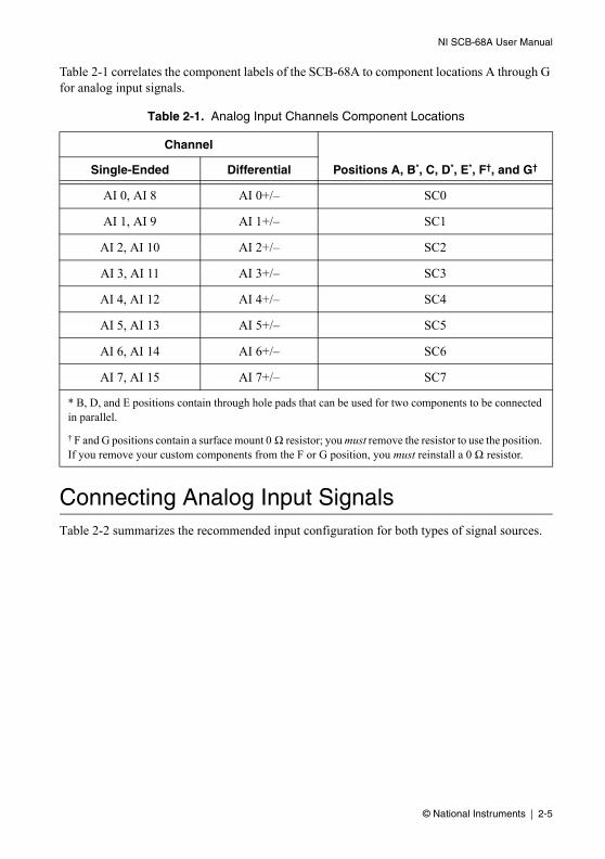
Table 2-1 correlates the component labels of the SCB-68A to component locations A through G for analog input signals.
Connecting Analog Input SignalsTable 2-2 summarizes the recommended input configuration for both types of signal sources.
Table 2-1. Analog Input Channels Component Locations
Channel
Positions A, B*, C, D*, E*, F†, and G†Single-Ended Differential
AI 0, AI 8 AI 0+/– SC0
AI 1, AI 9 AI 1+/– SC1
AI 2, AI 10 AI 2+/– SC2
AI 3, AI 11 AI 3+/– SC3
AI 4, AI 12 AI 4+/– SC4
AI 5, AI 13 AI 5+/– SC5
AI 6, AI 14 AI 6+/– SC6
AI 7, AI 15 AI 7+/– SC7
* B, D, and E positions contain through hole pads that can be used for two components to be connected in parallel.
† F and G positions contain a surface mount 0 Ω resistor; you must remove the resistor to use the position. If you remove your custom components from the F or G position, you must reinstall a 0 Ω resistor.
2-6 | ni.com
Chapter 2 Analog Input and Temperature Sensor Measurements
Table 2-2. Analog Input Configuration
AI Ground-Reference
Setting*
Floating Signal Sources (Not Connected to Building Ground)
Ground-Referenced Signal Sources*
Examples:
• Ungrounded thermocouples
• Signal conditioning with isolated outputs
• Battery devices
Example:
• Plug-in instruments with non-isolated outputs
Differential (DIFF)
Non-Referenced Single-Ended (NRSE)
Referenced Single-Ended (RSE)
* Refer to the documentation for your DAQ device for descriptions of the RSE, NRSE, and DIFF modes, analog input signal sources, and software considerations.
+ –
+
–
AI+
AI–
AI GND
Signal Source DAQ Device
+–
+
–
AI+
AI–
AI GND
Signal Source DAQ Device
+–
+
–
AI
AI SENSE
AI GND
Signal Source DAQ Device
+–
+
–
AI
AI SENSE
AI GND
Signal Source DAQ Device
+–
+
–
AI
AI GND
Signal Source DAQ Device
Ground-loop potential (VA – VB) are addedto measured signal.
NOT RECOMMENDED
+–
+
–
AI
AI GNDVB
VA
Signal Source DAQ Device

© National Instruments | 2-7
NI SCB-68A User Manual
Floating Signal SourcesA floating signal source is not connected to the building ground system, but has an isolated ground-reference point. Some examples of floating signal sources are outputs of transformers, thermocouples, battery-powered devices, optical isolators, and isolation amplifiers. An instrument or device that has an isolated output is a floating signal source.
When to Use Differential Connections with Floating Signal SourcesUse differential input connections for any channel that meets any of the following conditions:
• The input signal is low-level (less than 1 V).
• The leads connecting the signal to the device are greater than 3 m (10 ft).
• The input signal requires a separate ground-reference point or return signal.
• The signal leads travel through noisy environments.
• Two analog input channels, AI+ and AI–, are available for the signal.
Differential signal connections reduce noise pickup and increase common-mode noise rejection. Differential signal connections also allow input signals to float within the common-mode limits of the NI-PGIA.
Refer to the Using Differential Connections for Floating Signal Sources section for more information about differential connections.
When to Use Non-Referenced Single-Ended (NRSE) Connections with Floating Signal SourcesOnly use NRSE input connections if the input signal meets the following conditions:
• The input signal is high-level (greater than 1 V).
• The leads connecting the signal to the device are less than 3 m (10 ft).
Differential input connections are recommended for greater signal integrity for any input signal that does not meet the preceding conditions.
In the single-ended modes, more electrostatic and magnetic noise couples into the signal connections than in differential configurations. The coupling is the result of differences in the signal path. Magnetic coupling is proportional to the area between the two signal conductors. Electrical coupling is a function of how much the electric field differs between the two conductors.
With this type of connection, the NI-PGIA rejects both the common-mode noise in the signal and the ground potential difference between the signal source and the device ground.
Refer to the documentation for your DAQ device for more information about NRSE connections.

2-8 | ni.com
Chapter 2 Analog Input and Temperature Sensor Measurements
When to Use Referenced Single-Ended (RSE) Connections with Floating Signal SourcesOnly use RSE input connections if the input signal meets the following conditions:
• The input signal can share a common reference point, AI GND, with other signals that use RSE.
• The input signal is high-level (greater than 1 V).
• The leads connecting the signal to the device are less than 3 m (10 ft).
Differential input connections are recommended for greater signal integrity for any input signal that does not meet the preceding conditions.
In the single-ended modes, more electrostatic and magnetic noise couples into the signal connections than in differential configurations. The coupling is the result of differences in the signal path. Magnetic coupling is proportional to the area between the two signal conductors. Electrical coupling is a function of how much the electric field differs between the two conductors.
With this type of connection, the NI-PGIA rejects both the common-mode noise in the signal and the ground potential difference between the signal source and the device ground.
Refer to the documentation for your DAQ device for more information about RSE connections.
Using Differential Connections for Floating Signal SourcesIt is important to connect the negative lead of a floating source to AI GND (either directly or through a bias resistor). Otherwise, the source can float out of the maximum working voltage range of the NI-PGIA and the DAQ device returns erroneous data.
The easiest way to reference the source to AI GND is to connect the positive side of the signal to AI+ and connect the negative side of the signal to AI GND as well as to AI– without using resistors. This connection works well for DC-coupled sources with low source impedance (<100 Ω).
Figure 2-4. Differential Connections for Floating Signal Sources without Bias Resistors
–
+
Inpedance<100 Ω
AI GND
AI+
AI–
AI SENSE
Vs
FloatingSignal
Source
DAQ Device
© National Instruments | 2-9
NI SCB-68A User Manual
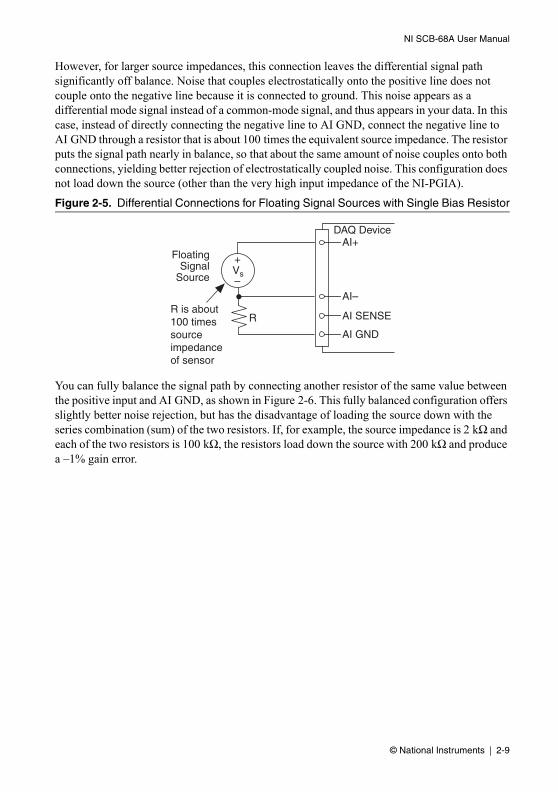
However, for larger source impedances, this connection leaves the differential signal path significantly off balance. Noise that couples electrostatically onto the positive line does not couple onto the negative line because it is connected to ground. This noise appears as a differential mode signal instead of a common-mode signal, and thus appears in your data. In this case, instead of directly connecting the negative line to AI GND, connect the negative line to AI GND through a resistor that is about 100 times the equivalent source impedance. The resistor puts the signal path nearly in balance, so that about the same amount of noise couples onto both connections, yielding better rejection of electrostatically coupled noise. This configuration does not load down the source (other than the very high input impedance of the NI-PGIA).
Figure 2-5. Differential Connections for Floating Signal Sources with Single Bias Resistor
You can fully balance the signal path by connecting another resistor of the same value between the positive input and AI GND, as shown in Figure 2-6. This fully balanced configuration offers slightly better noise rejection, but has the disadvantage of loading the source down with the series combination (sum) of the two resistors. If, for example, the source impedance is 2 kΩ and each of the two resistors is 100 kΩ, the resistors load down the source with 200 kΩ and produce a –1% gain error.
–
+
R is about 100 times source impedanceof sensor
AI GND
R
Vs
FloatingSignal
Source
AI+
AI–
AI SENSE
DAQ Device

2-10 | ni.com
Chapter 2 Analog Input and Temperature Sensor Measurements
Figure 2-6. Floating Signal Source Differential Connections with Balanced Bias Resistors
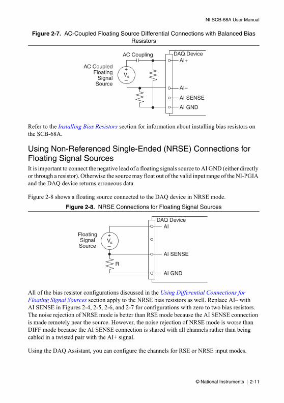
Both inputs of the NI-PGIA require a DC path to ground in order for the NI-PGIA to work. If the source is AC coupled (capacitively coupled), the NI-PGIA needs a resistor between the positive input and AI GND. If the source has low-impedance, choose a resistor that is large enough not to significantly load the source, but small enough not to produce significant input offset voltage as a result of input bias current (typically 100 kΩ to 1 MΩ). In this case, connect the negative input directly to AI GND. If the source has high output impedance, balance the signal path as previously described using the same value resistor on both the positive and negative inputs; be aware that there is some gain error from loading down the source, as shown in Figure 2-7.
DAQ Device Configured in Differential Mode
PGIA
–
+
–
+
–
+
FloatingSignalSource
BiasCurrentReturnPaths
AI GND
AI SENSE
Input Multiplexers
MeasuredVoltage
InstrumentationAmplifier
AI+
AI–
I/O Connector
BiasResistors(see text)
Vs
Vm
© National Instruments | 2-11
NI SCB-68A User Manual
Figure 2-7. AC-Coupled Floating Source Differential Connections with Balanced Bias Resistors
Refer to the Installing Bias Resistors section for information about installing bias resistors on the SCB-68A.
Using Non-Referenced Single-Ended (NRSE) Connections for Floating Signal SourcesIt is important to connect the negative lead of a floating signals source to AI GND (either directly or through a resistor). Otherwise the source may float out of the valid input range of the NI-PGIA and the DAQ device returns erroneous data.
Figure 2-8 shows a floating source connected to the DAQ device in NRSE mode.
Figure 2-8. NRSE Connections for Floating Signal Sources
All of the bias resistor configurations discussed in the Using Differential Connections for Floating Signal Sources section apply to the NRSE bias resistors as well. Replace AI– with AI SENSE in Figures 2-4, 2-5, 2-6, and 2-7 for configurations with zero to two bias resistors. The noise rejection of NRSE mode is better than RSE mode because the AI SENSE connection is made remotely near the source. However, the noise rejection of NRSE mode is worse than DIFF mode because the AI SENSE connection is shared with all channels rather than being cabled in a twisted pair with the AI+ signal.
Using the DAQ Assistant, you can configure the channels for RSE or NRSE input modes.
–
+
AI GND
Vs
AC CoupledFloating
SignalSource
AI+
AI–
AI SENSE
AC Coupling DAQ Device
–
+
AI GND
R
AI SENSE
AI
Vs
FloatingSignalSource
DAQ Device
2-12 | ni.com
Chapter 2 Analog Input and Temperature Sensor Measurements
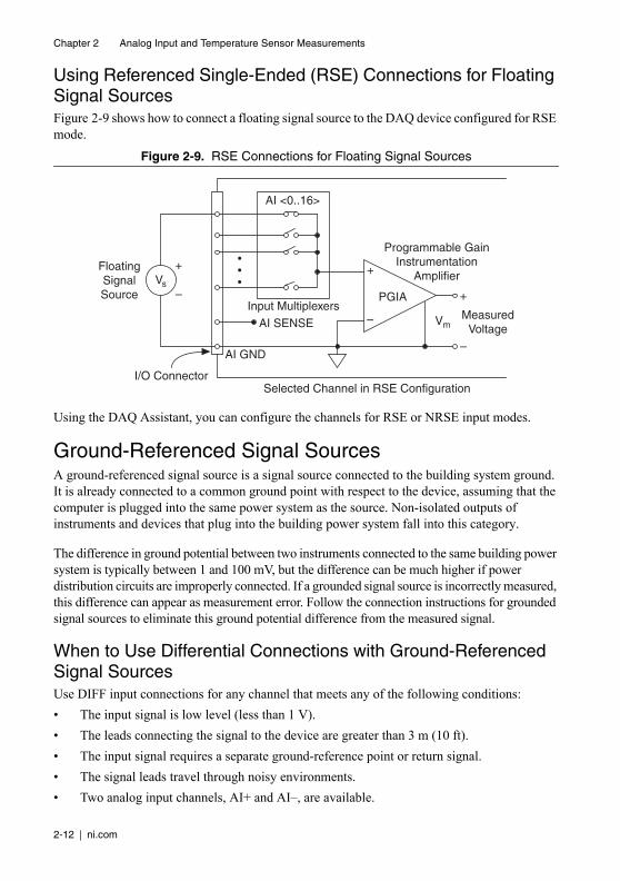
Using Referenced Single-Ended (RSE) Connections for Floating Signal SourcesFigure 2-9 shows how to connect a floating signal source to the DAQ device configured for RSE mode.
Figure 2-9. RSE Connections for Floating Signal Sources
Using the DAQ Assistant, you can configure the channels for RSE or NRSE input modes.
Ground-Referenced Signal SourcesA ground-referenced signal source is a signal source connected to the building system ground. It is already connected to a common ground point with respect to the device, assuming that the computer is plugged into the same power system as the source. Non-isolated outputs of instruments and devices that plug into the building power system fall into this category.
The difference in ground potential between two instruments connected to the same building power system is typically between 1 and 100 mV, but the difference can be much higher if power distribution circuits are improperly connected. If a grounded signal source is incorrectly measured, this difference can appear as measurement error. Follow the connection instructions for grounded signal sources to eliminate this ground potential difference from the measured signal.
When to Use Differential Connections with Ground-Referenced Signal SourcesUse DIFF input connections for any channel that meets any of the following conditions:
• The input signal is low level (less than 1 V).
• The leads connecting the signal to the device are greater than 3 m (10 ft).
• The input signal requires a separate ground-reference point or return signal.
• The signal leads travel through noisy environments.
• Two analog input channels, AI+ and AI–, are available.
Selected Channel in RSE Configuration
PGIAInput Multiplexers
–
+
–
Floating Signal Source
Vs
I/O Connector
AI GND
AI SENSE
AI <0..16>
+
Programmable GainInstrumentation
Amplifier
MeasuredVoltage
Vm
–
+

© National Instruments | 2-13
NI SCB-68A User Manual
DIFF signal connections reduce noise pickup and increase common-mode noise rejection. DIFF signal connections also allow input signals to float within the common-mode limits of the NI-PGIA.
Refer to the Using Differential Connections for Ground-Referenced Signal Sources section for more information about differential connections.
When to Use Non-Referenced Single-Ended (NRSE) Connections with Ground-Referenced Signal SourcesOnly use NRSE connections if the input signal meets the following conditions:
• The input signal is high-level (greater than 1 V).
• The leads connecting the signal to the device are less than 3 m (10 ft).
• The input signal can share a common reference point with other signals.
DIFF input connections are recommended for greater signal integrity for any input signal that does not meet the preceding conditions.
In the single-ended modes, more electrostatic and magnetic noise couples into the signal connections than in DIFF configurations. The coupling is the result of differences in the signal path. Magnetic coupling is proportional to the area between the two signal conductors. Electrical coupling is a function of how much the electric field differs between the two conductors.
With this type of connection, the NI-PGIA rejects both the common-mode noise in the signal and the ground potential difference between the signal source and the device ground.
Refer to the Using Non-Referenced Single-Ended (NRSE) Connections for Ground-Referenced Signal Sources section for more information about NRSE connections.
When to Use Referenced Single-Ended (RSE) Connections with Ground-Referenced Signal SourcesDo not use RSE connections with ground-referenced signal sources. Use NRSE or DIFF connections instead.
As shown in the bottom-rightmost cell of Table 2-2, there can be a potential difference between AI GND and the ground of the sensor. In RSE mode, this ground loop causes measurement errors.
2-14 | ni.com
Chapter 2 Analog Input and Temperature Sensor Measurements
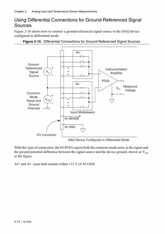
Using Differential Connections for Ground-Referenced Signal SourcesFigure 2-10 shows how to connect a ground-referenced signal source to the DAQ device configured in differential mode.
Figure 2-10. Differential Connections for Ground-Referenced Signal Sources
With this type of connection, the NI-PGIA rejects both the common-mode noise in the signal and the ground potential difference between the signal source and the device ground, shown as Vcm in the figure.
AI+ and AI– must both remain within ±11 V of AI GND.
DAQ Device Configured in Differential Mode
PGIA
–
+
–
+
–
+
–
+
Vcm
Vs
Ground-Referenced
SignalSource
Common-Mode
Noise andGroundPotential
AI GND
AI SENSE
Input Multiplexers
VmMeasured
Voltage
InstrumentationAmplifier
AI+
AI–
I/O Connector

© National Instruments | 2-15
NI SCB-68A User Manual
Using Non-Referenced Single-Ended (NRSE) Connections for Ground-Referenced Signal SourcesFigure 2-11 shows how to connect ground-reference signal sources in NRSE mode.
Figure 2-11. Single-Ended Connections for Ground-Referenced Signal Sources (NRSE Configuration)
AI <0..x> and AI SENSE must both remain within ±11 V of AI GND.
To measure a single-ended, ground-referenced signal source, you must use the NRSE ground-reference setting. Connect the signal to one of AI <0..x> and connect the signal local ground reference to AI SENSE. AI SENSE is internally connected to the negative input of the NI-PGIA. Therefore, the ground point of the signal connects to the negative input of the NI-PGIA.
Any potential difference between the device ground and the signal ground appears as a common-mode signal at both the positive and negative inputs of the NI-PGIA, and this difference is rejected by the amplifier. If the input circuitry of a device were referenced to ground, as it is in the RSE ground-reference setting, this difference in ground potentials would appear as an error in the measured voltage.
You can configure the channels for RSE or NRSE input modes using DAQ Assistant.
DAQ Device Configured in NRSE Mode
Input Multiplexers
I/O Connector
AI GND
AI SENSE
AI <0..16>
–
+
–
+Vcm
Vs
Ground-Referenced
SignalSource
Common-ModeNoise
and GroundPotential
PGIA
–
+
–
+
VmMeasured
Voltage
InstrumentationAmplifier
2-16 | ni.com
Chapter 2 Analog Input and Temperature Sensor Measurements
Using the Temperature SensorTo accommodate thermocouples with DAQ devices, the SCB-68A has a temperature sensor for cold-junction compensation (CJC), shown in Figure 1-2, SCB-68A Printed Circuit Board Diagram. To power the temperature sensor, set the switches for single-ended or differential mode as described in the Using the SCB-68A with MIO DAQ Devices section of Chapter 1, Getting Started with the SCB-68A. This configuration also powers the signal conditioning area and circuitry. Refer to Figure 2-1 for a diagram of the CJC circuitry on the SCB-68A.
Taking Thermocouple MeasurementsYou can measure thermocouples in differential or single-ended configuration:
• Differential configuration has better noise immunity. Use bias resistors when the DAQ device is in differential input mode, as described in the Installing Bias Resistors section.
• Single-ended configuration has twice as many inputs. For single-ended configuration, set your DAQ device for referenced single-ended (RSE) input mode.
The maximum voltage level thermocouples generate is typically only a few millivolts. You should use a DAQ device with high gain for best resolution. For more information about thermocouple measurements, refer to the NI Developer Zone tutorial, Taking Thermocouple Temperature Measurements. To access this document, go to ni.com/info and enter the Info Code rdtttm.
The DAQ device must have a ground reference because thermocouples are floating signal sources. For more information about floating signal sources, refer to the Connecting Analog Input Signals section. For more information about field wiring, refer to the NI Developer Zone document, Field Wiring and Noise Considerations for Analog Signals. To access this document, go to ni.com/info and enter the Info Code rdfwn3.
CJC with the SCB-68A is accurate only if the temperature sensor reading is close to the actual temperature of the screw terminals. Therefore, when reading thermocouples, keep the SCB-68A away from drafts or other temperature gradients, such as those caused by heaters, radiators, fans, and warm equipment.

© National Instruments | 2-17
NI SCB-68A User Manual
Temperature Sensor Output and AccuracyThe SCB-68A temperature sensor outputs 10 mV/°C and has an accuracy of ±1 °C.
You also can determine the temperature using the following formulas:
TC = 100 × Vt
TK = TC + 273.15
where Vt is the temperature sensor output voltage;
and TC, TK, and TF are the temperature readings in degrees Celsius, Kelvin, and Fahrenheit, respectively.
Thermocouple Sources of ErrorWhen taking thermocouple measurements with the SCB-68A, the possible sources of error are as follows:
• Compensation error—Can arise from two sources—inaccuracy of the temperature sensor and temperature differences between the temperature sensor and the screw terminals. The temperature sensor on the SCB-68A is specified to be accurate to ±1 °C. You can minimize temperature differences between the temperature sensor and the screw terminals by keeping the SCB-68A away from drafts, heaters, and warm equipment.
• Linearization error—A consequence of the polynomials being approximations of the true thermocouple output. The linearization error depends upon the degree of polynomial used.
• Measurement error—The result of inaccuracies in the DAQ device. These inaccuracies include gain, offset, and noise. Accuracy can be calculated from the DAQ device specifications. For best results, you must use a well-calibrated DAQ device. NI recommends that you run self-calibration on your DAQ device frequently to reduce error.
• Thermocouple wire error—The result of inconsistencies in the thermocouple manufacturing process. These inconsistencies, or nonhomogeneities, are the result of defects or impurities in the thermocouple wire. The errors vary depending on the thermocouple type and the gauge of wire used, but an error of ±2 °C is typical. For more information about thermocouple wire errors and more specific data, consult the thermocouple manufacturer.
• Noise error—Error due to inherent system noise. Use the average of a large number of samples to obtain the most accurate reading. Noisy environments require averaging more samples for greater accuracy.
TF95--- TC× 32+=
white noise
number of samples------------------------------------------------- resulting noise=

2-18 | ni.com
Chapter 2 Analog Input and Temperature Sensor Measurements
For best results, use the average of at least 100 readings to reduce the effects of noise; typical absolute accuracies should then be about ±2 °C.
Open Thermocouple DetectionYou can build open thermocouple detection circuitry by connecting a high-value resistor between the positive input and +5 V. A resistor of a few MΩ or more is sufficient, but a high-value resistor allows you to detect an open or defective thermocouple.
Note Refer to the Soldering and Desoldering Components on the SCB-68A section of Chapter 1, Getting Started with the SCB-68A, for more information about adding components and for soldering and desoldering instructions.
• Differential analog input open thermocouple detection—Use position A to connect a high-value resistor between the positive input and +5 V. Leave the 0 Ω resistors at positions F and G in place for each channel used. Refer to Table 2-1 for component positions for all analog input channels.
Figure 2-12. Differential Analog Input Open Thermocouple Detection
AIi
AIi+8
ySCx
E
A
FG
B
C D
+
+
+
–
+5 V AI GND
+5 V AI GND
AI i
AI i + 8

© National Instruments | 2-19
NI SCB-68A User Manual
• Single-ended analog input open thermocouple detection—Use position A for one channel and C for the next channel when you connect a high-value resistor between the positive input and +5 V. Leave the 0 Ω resistors at positions F and G in place for each channel used. Refer to Table 2-1 for component positions for all analog input channels.
Figure 2-13. Single-Ended Analog Input Open Thermocouple Detection on AI <i>
If the thermocouple opens, the voltage measured across the input terminals rises to +5 V, a value much larger than any legitimate thermocouple voltage. You can create a bias current return path by using a 100 kΩ resistor between the negative input and AI GND.
Thermocouple Input FilteringTo reduce noise, you can connect a simple one-pole RC lowpass filter to the analog inputs of the SCB-68A. Refer to the One-Pole Lowpass RC Filter section for more information.
AIi
AIi+8
ySCx
E
A
FG
B
C D
+
+
+
–
+5 V AI GND
+5 V AI GND
AI i
AI i + 8

2-20 | ni.com
Chapter 2 Analog Input and Temperature Sensor Measurements
Installing Bias ResistorsTo install a single bias resistor on the negative line (AI–) of a differential pair, put the resistor in position D on the SCB-68A, as shown in Figure 2-14. Leave the 0 Ω resistors at positions F and G in place for each channel used.
Figure 2-14. AI Differential Configuration with Single Bias Resistor
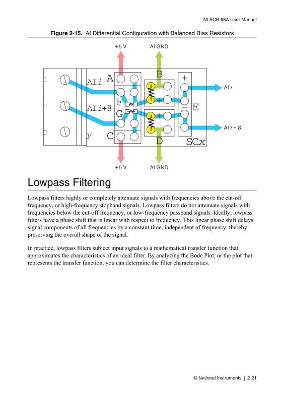
To install balanced bias resistors, put resistors in positions B and D on the SCB-68A, as shown in Figure 2-15. Leave the 0 Ω resistors at positions F and G in place for each channel used.
AIi
AIi+8
ySCx
E
A
FG
B
C D
+
+
+
–
+5 V AI GND
+5 V AI GND
AI i
AI i + 8
© National Instruments | 2-21
NI SCB-68A User Manual
Figure 2-15. AI Differential Configuration with Balanced Bias Resistors
Lowpass FilteringLowpass filters highly or completely attenuate signals with frequencies above the cut-off frequency, or high-frequency stopband signals. Lowpass filters do not attenuate signals with frequencies below the cut-off frequency, or low-frequency passband signals. Ideally, lowpass filters have a phase shift that is linear with respect to frequency. This linear phase shift delays signal components of all frequencies by a constant time, independent of frequency, thereby preserving the overall shape of the signal.
In practice, lowpass filters subject input signals to a mathematical transfer function that approximates the characteristics of an ideal filter. By analyzing the Bode Plot, or the plot that represents the transfer function, you can determine the filter characteristics.
AIi
AIi+8
ySCx
E
A
FG
B
C D
+
+
+
–
+5 V AI GND
+5 V AI GND
AI i
AI i + 8

2-22 | ni.com
Chapter 2 Analog Input and Temperature Sensor Measurements
Figures 2-16 and 2-17 show the Bode Plots for the ideal filter and the real filter, respectively, and indicate the attenuation of each transfer function.
Figure 2-16. Transfer Function Attenuation for an Ideal Filter
Figure 2-17. Transfer Function Attenuation for a Real Filter
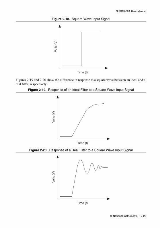
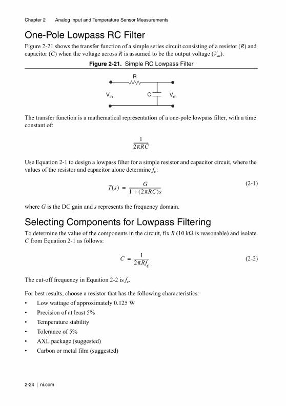
The cut-off frequency, fc, is defined as the frequency beyond which the gain drops 3 dB. Figure 2-16 shows how an ideal filter causes the gain to drop to zero for all frequencies greater than fc. Thus, fc does not pass through the filter to its output. Instead of having a gain of absolute zero for frequencies greater than fc, the real filter has a transition region between the passband and the stopband, a ripple in the passband, and a stopband with a finite attenuation gain.
Real filters have some nonlinearity in their phase response, causing signals at higher frequencies to be delayed longer than signals at lower frequencies and resulting in an overall shape distortion of the signal. For example, when the square wave, shown in Figure 2-18, enters a filter, an ideal filter smooths the edges of the input, whereas a real filter causes some ringing in the signal as the higher frequency components of the signal are delayed.
Passband
Stopband
Log Frequency
Gai
n
fc
Passband
Stopband
Log Frequency
Gai
n
fc
TransitionRegion
© National Instruments | 2-23
NI SCB-68A User Manual
Figure 2-18. Square Wave Input Signal
Figures 2-19 and 2-20 show the difference in response to a square wave between an ideal and a real filter, respectively.
Figure 2-19. Response of an Ideal Filter to a Square Wave Input Signal
Figure 2-20. Response of a Real Filter to a Square Wave Input Signal
Time (t)
Vol
ts (
V)
Time (t)
Vol
ts (
V)
Time (t)
Vol
ts (
V)
2-24 | ni.com
Chapter 2 Analog Input and Temperature Sensor Measurements
One-Pole Lowpass RC FilterFigure 2-21 shows the transfer function of a simple series circuit consisting of a resistor (R) and capacitor (C) when the voltage across R is assumed to be the output voltage (Vm).
Figure 2-21. Simple RC Lowpass Filter
The transfer function is a mathematical representation of a one-pole lowpass filter, with a time constant of:
Use Equation 2-1 to design a lowpass filter for a simple resistor and capacitor circuit, where the values of the resistor and capacitor alone determine fc:
(2-1)
where G is the DC gain and s represents the frequency domain.
Selecting Components for Lowpass FilteringTo determine the value of the components in the circuit, fix R (10 kΩ is reasonable) and isolate C from Equation 2-1 as follows:
(2-2)
The cut-off frequency in Equation 2-2 is fc.
For best results, choose a resistor that has the following characteristics:
• Low wattage of approximately 0.125 W
• Precision of at least 5%
• Temperature stability
• Tolerance of 5%
• AXL package (suggested)
• Carbon or metal film (suggested)
R
CVin Vm
12πRC---------------
T s( ) G1 2πRC( )s+-------------------------------=
C1
2πRfc---------------=

© National Instruments | 2-25
NI SCB-68A User Manual
Choose a capacitor that has the following suggested characteristics:
• AXL or RDL package
• Tolerance of 20%
• Maximum voltage of at least 25 V
Adding Components for Lowpass Filters on Analog Input SignalsUsing the circuit shown in Figure 2-21, you can use a two-component circuit to build a simple RC filter with analog input. You can build a lowpass filter for the following analog input modes:
• Differential analog input lowpass filter—To build a differential lowpass filter, refer to Figure 2-22. Add the resistor to position F and the capacitor to position E. Refer to Table 2-1 for component positions for all analog input channels.
The SCB-68A ships with a surface mount 0 Ω resistor in the F position. You must remove the resistor to use the position.
Figure 2-22. SCB-68A Circuit Diagram for Differential Analog Input Lowpass Filter
• Single-ended analog input lowpass filter—To build a single-ended lowpass filter, refer to Figure 2-23. Add the resistor to position F or G, depending on the AI channel you are using. Add the capacitor to position B or D, depending on the AI channel you are using. Refer to Table 2-1 for component positions for all analog input channels.
The SCB-68A ships with a surface mount 0 Ω resistors in the F and G positions. You must remove the resistor to use the position.
AIi
AIi+8
ySCx
E
A
FG
B
C D
+
+
+
+5 V AI GND
+5 V AI GND
AI i
AI i + 8

2-26 | ni.com
Chapter 2 Analog Input and Temperature Sensor Measurements
Note Filtering increases the settling time of the instrumentation amplifier to the time constant of the filter used. Adding RC filters to scanning channels greatly reduces the practical scanning rate, since the instrumentation amplifier settling time can be increased to 10T or longer, where T = (R)(C).
Figure 2-23. SCB-68A Circuit Diagram for Single-Ended Analog Input Lowpass Filter on AI <i>
Analog Input Lowpass Filtering ApplicationsThe following applications benefit from lowpass filtering:
• Noise filtering—You can use a lowpass filter to highly attenuate the noise frequency on a measured signal. For example, power lines commonly add a noise frequency of 60 Hz. Adding a filter with fc<60 Hz at the input of the measurement system causes the noise frequency to fall into the stopband.
Referring to Equation 2-2, fix the resistor value at 10 kΩ to calculate the capacitor value and choose a commercial capacitor value that satisfies the following relationship:
(2-3)
AIi
AIi+8
ySCx
E
A
FG
B
C D
+
+
+
+5 V AI GND
+5 V AI GND
AI i
AI i + 8
C1
2π 10 000,( ) 60( )----------------------------------------->

© National Instruments | 2-27
NI SCB-68A User Manual
• Antialiasing filtering—Aliasing causes high-frequency signal components to appear as a low-frequency signal, as Figure 2-24 shows.
Figure 2-24. Aliasing of a High-Frequency Signal
The solid line depicts a high-frequency signal being sampled at the indicated points. When these points are connected to reconstruct the waveform, as shown by the dotted line, the signal appears to have a lower frequency. Any signal with a frequency greater than one-half of its sample rate is aliased and incorrectly analyzed as having a frequency below one-half the sample rate. This limiting frequency of one-half the sample rate is called the Nyquist frequency.
To prevent aliasing, remove all signal components with frequencies greater than the Nyquist frequency from input signals before those signals are sampled. Once a data sample is aliased, it is impossible to accurately reconstruct the original signal.
To design a lowpass filter that attenuates signal components with a frequency higher than half of the Nyquist frequency, substitute the half Nyquist value for the fc value in Equation 2-3.
Note (NI 6115/6120/6289 Devices Only) Some devices, such as the NI 6115/6120/6289, provide filters and may not need antialiasing filters implemented at the SCB-68A terminal block. Refer to your device documentation for more information.
Highpass FilteringHighpass filters highly or completely attenuate signals with frequencies below the cut-off frequency, or low-frequency stopband signals. Highpass filters do not attenuate signals with frequencies above the cut-off frequency, or high-frequency passband signals.
The cut-off frequency, fc, is defined as the frequency below which the gain drops 3 dB. Figure 2-25 shows how an ideal filter causes the gain to drop to zero for all frequencies less than fc. Thus, fc does not pass through the filter to its output.
2 4 6 8 100
1
–1
Input SignalSampled PointsReconstructed Signal

2-28 | ni.com
Chapter 2 Analog Input and Temperature Sensor Measurements
In practice, highpass filters subject input signals to a mathematical transfer function that approximates the characteristics of an ideal filter. By analyzing the Bode Plot, or the plot that represents the transfer function, you can determine the filter characteristics.
Figures 2-25 and 2-26 show the Bode Plots for the ideal filter and the real filter, respectively, and indicate the attenuation of each transfer function.
Figure 2-25. Transfer Function Attenuation for an Ideal Filter
Figure 2-26. Transfer Function Attenuation for a Real Filter
Instead of having a gain of absolute zero for frequencies less than fc, the real filter has a transition region between the passband and the stopband, a ripple in the passband, and a stopband with a finite attenuation gain.
Passband
Stopband
Log Frequency
Gai
n
fc
Passband
Stopband
Log Frequency
Gai
n
fc
TransitionRegion

© National Instruments | 2-29
NI SCB-68A User Manual
One-Pole Highpass RC FilterFigure 2-27 shows the transfer function of a simple series circuit consisting of a resistor (R) and capacitor (C) when the voltage across R is assumed to be the output voltage (Vm).
Figure 2-27. Simple RC Highpass Circuit
The transfer function is a mathematical representation of a one-pole highpass filter, with a time constant of:
Use Equation 2-4 to design a lowpass filter for a simple resistor and capacitor circuit, where the values of the resistor and capacitor alone determine fc:
(2-4)
where G is the DC gain and s represents the frequency domain.
Selecting Components for Highpass FilteringTo determine the value of the components in the circuit, fix R (10 kΩ is reasonable) and isolate C from Equation 2-4 as follows:
(2-5)
The cutoff frequency in Equation 2-5 is fc.
For best results, choose a resistor that has the following characteristics:
• Low wattage of approximately 0.125 W
• Precision of at least 5%
• Temperature stability
• Tolerance of 5%
• AXL package (suggested)
• Carbon or metal film (suggested)
R
C
Vin Vout
12πRC---------------
T s( ) G1 2πRC( )s+-------------------------------=
C1
2πRfc---------------=
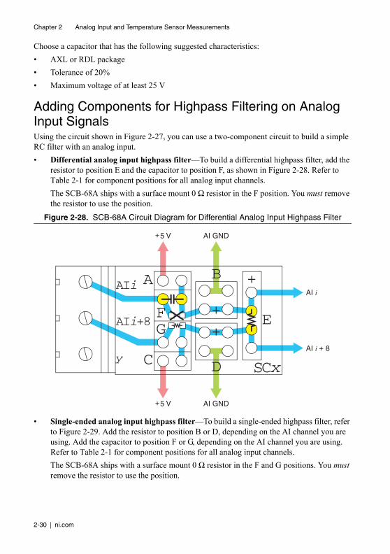
2-30 | ni.com
Chapter 2 Analog Input and Temperature Sensor Measurements
Choose a capacitor that has the following suggested characteristics:
• AXL or RDL package
• Tolerance of 20%
• Maximum voltage of at least 25 V
Adding Components for Highpass Filtering on Analog Input SignalsUsing the circuit shown in Figure 2-27, you can use a two-component circuit to build a simple RC filter with an analog input.
• Differential analog input highpass filter—To build a differential highpass filter, add the resistor to position E and the capacitor to position F, as shown in Figure 2-28. Refer to Table 2-1 for component positions for all analog input channels.
The SCB-68A ships with a surface mount 0 Ω resistor in the F position. You must remove the resistor to use the position.
Figure 2-28. SCB-68A Circuit Diagram for Differential Analog Input Highpass Filter
• Single-ended analog input highpass filter—To build a single-ended highpass filter, refer to Figure 2-29. Add the resistor to position B or D, depending on the AI channel you are using. Add the capacitor to position F or G, depending on the AI channel you are using. Refer to Table 2-1 for component positions for all analog input channels.
The SCB-68A ships with a surface mount 0 Ω resistor in the F and G positions. You must remove the resistor to use the position.
AIi
AIi+8
ySCx
E
A
FG
B
C D
+
+
+
+5 V AI GND
+5 V AI GND
AI i
AI i + 8

© National Instruments | 2-31
NI SCB-68A User Manual
Figure 2-29. SCB-68A Circuit Diagram for Single-Ended Analog Input Highpass Filter on AI <i>
Analog Input Highpass Filtering ApplicationsOne of the most common applications for highpass filters for analog inputs is to use the filter to do AC coupling. AC coupling can be achieved by creating a highpass filter with a very low cutoff frequency. This filter allows most dynamic signals through, while it blocks any DC offsets in the signal. This can be used to increase the resolution with which you can measure a dynamic signal that is riding on top of an offset, as shown in Figure 2-30.
Figure 2-30. Signal before Passing through Filter
AIi
AIi+8
ySCx
E
A
FG
B
C D
+
+
+
+5 V AI GND
+5 V AI GND
AI i
AI i + 8
10 V
0 VTime (t)

2-32 | ni.com
Chapter 2 Analog Input and Temperature Sensor Measurements
Without the AC coupling you would use the ±10 V range or the 0–10 V range. After passing through the filter, the dynamic portion of the signal is retained and centered around 0, as shown in Figure 2-31.
Figure 2-31. Signal after Passing through Filter
You can now reduce your range to ±1 V to increase the resolution of the measurement.
Current Input MeasurementSome DAQ devices cannot directly measure current. This section describes how to add components for measuring current up to 20 mA.
The conversion from current to voltage is based on Ohm’s Law, summarized by the following equation:
V = I × R
where V is voltage, I is current, and R is resistance.
By putting a resistor with a known value in series with the current and measuring the voltage produced across the resistor as shown in Figure 2-32, you can calculate the current flowing through the circuit.
Figure 2-32. Current-to-Voltage Electrical Circuit
0 V
Time (t)
I
RTransducerInput
Vin
+
–
+
–
© National Instruments | 2-33
NI SCB-68A User Manual
The application software must linearly convert voltage back to current. The following equation demonstrates this conversion, where the resistor is the denominator and Vin is the input voltage into the DAQ device:
Selecting a Resistor for Current Input MeasurementFor best results when measuring current, choose a resistor that has the following characteristics:
• Low wattage of approximately 0.125 W
• Precision of at least 5%
• Temperature stability
• Tolerance of 5%
• 232 Ω (suggested)
• AXL package (suggested)
• Carbon or metal film (suggested)
If you use the resistor described above, you can convert a 20 mA current to 4.64 V by setting the device range to either (–5 to +5 V) or (0 to 5 V).
Adding Components for Current Input Measurement on Analog Input Signals
Caution Do not exceed ±10 V at the analog inputs. NI is not liable for any device damage or personal injury resulting from improper connections.
You can build a one-resistor circuit for measuring current at the single-ended or differential inputs of the SCB-68A:
• Differential analog inputs—To build a one-resistor circuit that measures current at the differential inputs of the SCB-68A, add the resistor to position E for each differential channel pair that is used. Leave the 0 Ω resistors in place for positions F and G. Refer to Table 2-1 for component positions for all analog input channels. Calculate the current according to the following equation:
IVin
R-------=
IVm
RE-------=
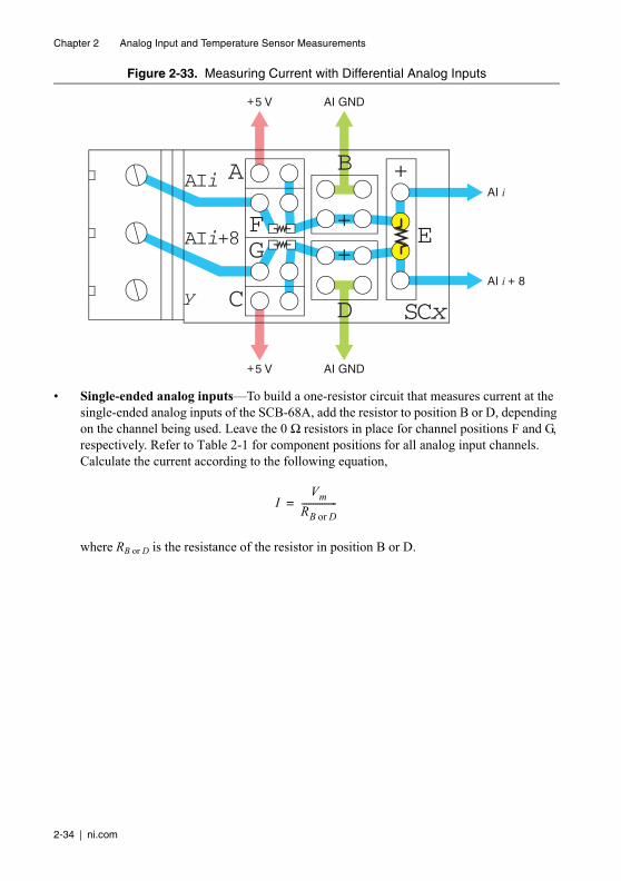
2-34 | ni.com
Chapter 2 Analog Input and Temperature Sensor Measurements
Figure 2-33. Measuring Current with Differential Analog Inputs
• Single-ended analog inputs—To build a one-resistor circuit that measures current at the single-ended analog inputs of the SCB-68A, add the resistor to position B or D, depending on the channel being used. Leave the 0 Ω resistors in place for channel positions F and G, respectively. Refer to Table 2-1 for component positions for all analog input channels. Calculate the current according to the following equation,
where RB or D is the resistance of the resistor in position B or D.
AIi
AIi+8
ySCx
E
A
FG
B
C D
+
+
+
+5 V AI GND
+5 V AI GND
AI i
AI i + 8
IVm
RB or D----------------=

© National Instruments | 2-35
NI SCB-68A User Manual
Figure 2-34. Measuring Current with Single-Ended Analog Input (AI <i>)
Attenuating VoltageTransducers can generate more than 10 VDC per channel, but DAQ devices cannot read more than 10 VDC per input channel. Therefore, you must attenuate output signals from the transducer to fit within the DAQ device specifications. Figure 2-35 shows how to use a voltage divider to attenuate the output signal of the transducer.
Figure 2-35. Attenuating Voltage with a Voltage Divider
The voltage divider splits the input voltage (Vin) between two resistors (R1 and R2), causing the voltage on each resistor to be noticeably lower than Vin. Use Equation 2-6 to determine the Vm that the DAQ device measures:
(2-6)
Use Equation 2-7 to determine the overall gain of a voltage divider circuit:
AIi
AIi+8
ySCx
E
A
FG
B
C D
+
+
+
+5 V AI GND
+5 V AI GND
AI i
AI i + 8
R2Vin Vm
+
–
+
–
R1
Vm Vin
R2
R1 R2+------------------ =

2-36 | ni.com
Chapter 2 Analog Input and Temperature Sensor Measurements
(2-7)
The accuracy of Equation 2-7 depends on the tolerances of the resistors that you use.
Caution The SCB-68A is not designed for any input voltages >30 Vrms/42 Vpk/60 VDC, even if a user-installed voltage divider reduces the voltage to within the input range of the DAQ device. Input voltages >30 Vrms/42 Vpk/60 VDC can damage the SCB-68A, any devices connected to it, and the host computer. Overvoltage can also cause an electric shock hazard for the operator.
Selecting Components for Attenuating VoltageTo set up the resistors, complete the following steps.
1. Select the value for R2 (10 kΩ is recommended).
2. Use Equation 2-6 to calculate the value for R1.
Base the R1 calculation on the following values:
• Maximum Vin you expect from the transducer
• Maximum voltage (<10 VDC) that you want to input to the DAQ device
Accuracy Considerations for Attenuating VoltageFor best results when attenuating voltage, choose a resistor that has the following characteristics:
• Low wattage of approximately 0.125 W
• Precision of at least 5%
• Temperature stable
• Tolerance of 5%
• AXL package (suggested)
• Carbon or metal film (suggested)
Verify that R1 and R2 drift together with respect to temperature; otherwise, the system may consistently read incorrect values.
GVm
Vin-------
R2
R1 R2+------------------= =
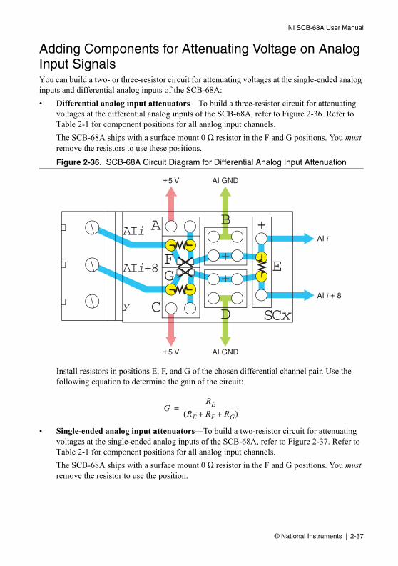
© National Instruments | 2-37
NI SCB-68A User Manual
Adding Components for Attenuating Voltage on Analog Input SignalsYou can build a two- or three-resistor circuit for attenuating voltages at the single-ended analog inputs and differential analog inputs of the SCB-68A:
• Differential analog input attenuators—To build a three-resistor circuit for attenuating voltages at the differential analog inputs of the SCB-68A, refer to Figure 2-36. Refer to Table 2-1 for component positions for all analog input channels.
The SCB-68A ships with a surface mount 0 Ω resistor in the F and G positions. You must remove the resistors to use these positions.
Figure 2-36. SCB-68A Circuit Diagram for Differential Analog Input Attenuation
Install resistors in positions E, F, and G of the chosen differential channel pair. Use the following equation to determine the gain of the circuit:
• Single-ended analog input attenuators—To build a two-resistor circuit for attenuating voltages at the single-ended analog inputs of the SCB-68A, refer to Figure 2-37. Refer to Table 2-1 for component positions for all analog input channels.
The SCB-68A ships with a surface mount 0 Ω resistor in the F and G positions. You must remove the resistor to use the position.
AIi
AIi+8
ySCx
E
A
FG
B
C D
+
+
+
+5 V AI GND
+5 V AI GND
AI i
AI i + 8
GRE
RE RF RG+ +( )--------------------------------------=

2-38 | ni.com
Chapter 2 Analog Input and Temperature Sensor Measurements
Figure 2-37. SCB-68A Circuit Diagram for Single-Ended Analog Input Attenuation on AI <i>
Install resistors in positions B and F, or positions D and G, depending on the channel you are using on the SCB-68A. Use the following equation to calculate the gain of the circuit:
where RB or D is the resistance of the resistor in position B or D, and RF or G is the resistance of the resistor in position F or G.
Analog Input Voltage DividersWhen calculating the values for R1 and R2, consider the input impedance value from the point of view of Vin, as shown in Figure 2-38.
Figure 2-38. Input Impedance Electrical Circuit
The following equation shows the relationship among all of the resistor values:
AIi
AIi+8
ySCx
E
A
FG
B
C D
+
+
+
+5 V AI GND
+5 V AI GND
AI i
AI i + 8
GRB orD
RB orD RF orG+( )-------------------------------------------=
R2Vin
+
–
+
–
R1
InputImpedance

© National Instruments | 2-39
NI SCB-68A User Manual
Zin is the new input impedance. Refer to the device specifications for the input impedance of your device.
Zin R1
R2 Input Impedance×( )R2 Input Impedance+( )
----------------------------------------------------------+=

© National Instruments | 3-1
3Analog Output Waveforms
This chapter covers many topics associated with generating analog output waveforms, including how to condition signals by adding components to the open component locations of the SCB-68A for lowpass filtering and attenuating voltage applications.
Caution Add components at your own risk. NI is not liable for any damage resulting from improperly added components.
In addition to the applications described in this chapter, you can build many other types of signal conditioning using the component pads and the general-purpose breadboard area of the SCB-68A. Refer to the Soldering and Desoldering Components on the SCB-68A section of Chapter 1, Getting Started with the SCB-68A, for more information about adding components and for soldering and desoldering instructions.
After building one of the applications described in this chapter or your custom circuitry, refer to the Setting up the SCB-68A section of Chapter 1, Getting Started with the SCB-68A, for instructions about how to configure the SCB-68A in Measurement & Automation Explorer (MAX). You can create virtual channels in MAX to create a custom scale or map your voltage ranges to the type of transducer that you use.
Analog Output Channel Pad ConfigurationWhen you use the SCB-68A with a 68-pin or 100-pin MIO DAQ device, you can use the component pads on the SCB-68A to condition two AO channels. Figure 3-1 shows the circuitry for both analog output channels on the SCB-68A.
Figure 3-1. Analog Output Circuitry
B
AO 0(I/O Pin 22)
A
AO GND(I/O Pin 55)
B
AO 1(I/O Pin 21)
AAO 1 Screw Terminal
AO GND(I/O Pin 54)
AO GND Screw Terminal
AO GND Screw Terminal
AO 0 Screw Terminal
SC8
SC9

3-2 | ni.com
Chapter 3 Analog Output Waveforms
Figure 3-2 illustrates the generic AO channel pad configuration.
Figure 3-2. Analog Output Channel Pad Configuration
Table 3-1 correlates the component labels of the SCB-68A to component locations A and B for analog output channels 0 and 1.
Lowpass FilteringLowpass filters highly or completely attenuate signals with frequencies above the cut-off frequency, or high-frequency stopband signals. Lowpass filters do not attenuate signals with frequencies below the cut-off frequency, or low-frequency passband signals. Ideally, lowpass
Table 3-1. Analog Output Channels Component Locations
Channel Positions A* and B†
AO 0 SC8
AO 1 SC9
* A position contains a surface mount 0 Ω resistor; you must remove the resistor to use the position. If you remove your custom components from the A position, you must reinstall a 0 Ω resistor.† B position contains through hole pads that can be used for two components to be connected in parallel.
56
22
55
21
54
20
SC8
SC9
A
A
B
B
+
+
AO 0
AO 1
AO GND
AO GND

© National Instruments | 3-3
NI SCB-68A User Manual
filters have a phase shift that is linear with respect to frequency. This linear phase shift delays signal components of all frequencies by a constant time, independent of frequency, thereby preserving the overall shape of the signal.
In practice, lowpass filters subject input signals to a mathematical transfer function that approximates the characteristics of an ideal filter. By analyzing the Bode Plot, or the plot that represents the transfer function, you can determine the filter characteristics.
Figures 3-3 and 3-4 show the Bode Plots for the ideal filter and the real filter, respectively, and indicate the attenuation of each transfer function.
Figure 3-3. Transfer Function Attenuation for an Ideal Filter
Figure 3-4. Transfer Function Attenuation for a Real Filter
The cut-off frequency, fc, is defined as the frequency beyond which the gain drops 3 dB. Figure 3-3 shows how an ideal filter causes the gain to drop to zero for all frequencies greater than fc. Thus, fc does not pass through the filter to its output. Instead of having a gain of absolute zero for frequencies greater than fc, the real filter has a transition region between the passband and the stopband, a ripple in the passband, and a stopband with a finite attenuation gain.
Real filters have some nonlinearity in their phase response, causing signals at higher frequencies to be delayed longer than signals at lower frequencies and resulting in an overall shape distortion
Passband
Stopband
Log Frequency
Gai
n
fc
Passband
Stopband
Log Frequency
Gai
n
fc
TransitionRegion
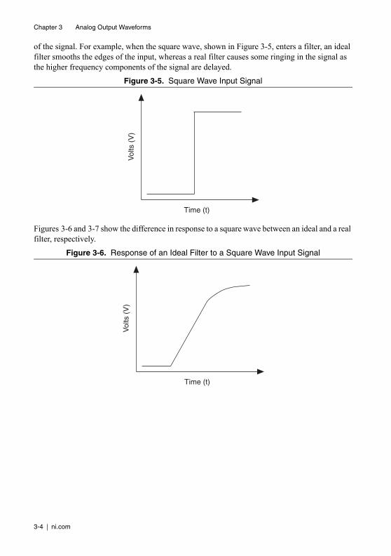
3-4 | ni.com
Chapter 3 Analog Output Waveforms
of the signal. For example, when the square wave, shown in Figure 3-5, enters a filter, an ideal filter smooths the edges of the input, whereas a real filter causes some ringing in the signal as the higher frequency components of the signal are delayed.
Figure 3-5. Square Wave Input Signal
Figures 3-6 and 3-7 show the difference in response to a square wave between an ideal and a real filter, respectively.
Figure 3-6. Response of an Ideal Filter to a Square Wave Input Signal
Time (t)
Vol
ts (
V)
Time (t)
Vol
ts (
V)

© National Instruments | 3-5
NI SCB-68A User Manual
Figure 3-7. Response of a Real Filter to a Square Wave Input Signal
One-Pole Lowpass RC FilterFigure 3-8 shows the transfer function of a simple series circuit consisting of a resistor (R) and capacitor (C) when the voltage across R is assumed to be the output voltage (Vm).
Figure 3-8. Simple RC Lowpass Filter
The transfer function is a mathematical representation of a one-pole lowpass filter, with a time constant of:
Use Equation 3-1 to design a lowpass filter for a simple resistor and capacitor circuit, where the values of the resistor and capacitor alone determine fc:
(3-1)
where G is the DC gain and s represents the frequency domain.
Time (t)
Vol
ts (
V)
R
CVin Vm
12πRC---------------
T s( ) G1 2πRC( )s+-------------------------------=

3-6 | ni.com
Chapter 3 Analog Output Waveforms
Selecting Components for Lowpass FilteringTo determine the value of the components in the circuit, fix R (10 kΩ is reasonable) and isolate C from Equation 3-1 as follows:
(3-2)
The cut-off frequency in Equation 3-2 is fc.
For best results, choose a resistor that has the following characteristics:
• Low wattage of approximately 0.125 W
• Precision of at least 5%
• Temperature stability
• Tolerance of 5%
• AXL package (suggested)
• Carbon or metal film (suggested)
Choose a capacitor that has the following suggested characteristics:
• AXL or RDL package
• Tolerance of 20%
• Maximum voltage of at least 25 V
Adding Components for Lowpass Smoothing Filters on Analog Output SignalsUsing the circuit shown in Figure 3-8, you can use a two-component circuit to build a simple RC filter with analog output. To build a lowpass filter for analog output, put a resistor in position A and a capacitor in position B, as shown in Figure 3-9.
The SCB-68A ships with a surface mount 0 Ω resistor in the A position. You must remove the resistor to use the position. Refer to Table 3-1 for component positions for both analog output channels.
C1
2πRfc---------------=

© National Instruments | 3-7
NI SCB-68A User Manual
Figure 3-9. SCB-68A Circuit Diagram for Analog Output Lowpass Filter
Analog Output Lowpass Filtering ApplicationsThe following applications benefit from lowpass filtering:
• Protection for external circuitry—Lowpass filters can smooth stairstep-like curves on AO signals. If the curves are not smoothed, the AO signals can be a hazard for some external circuitry connected to it. Figure 3-10 shows the output of a lowpass filter when a stairstep-like signal is the input.
Figure 3-10. Lowpass Filtering of AO Signals
• Deglitching analog output signals—Lowpass filters can be used to decrease glitches from an analog output signal. When you use a DAC to generate a waveform, you may observe glitches on the output signal. These glitches are normal; when a DAC switches from one voltage to another, it produces glitches due to released charges. The largest glitches occur when the most significant bit of the DAC code changes. You can build a lowpass deglitching filter to remove some of these glitches, depending on the frequency and nature of the output signal. To select a cutoff frequency for the deglitching filter, refer to your DAQ device documentation for the maximum glitch duration.
56
22
55
SC8
A
B+
AO 0
AO GND
Time (t)
Vol
ts (
V)
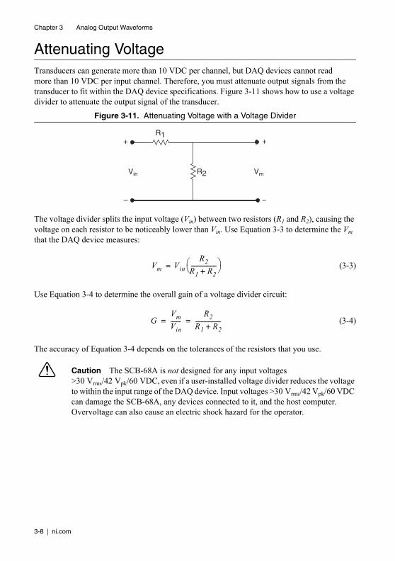
3-8 | ni.com
Chapter 3 Analog Output Waveforms
Attenuating VoltageTransducers can generate more than 10 VDC per channel, but DAQ devices cannot read more than 10 VDC per input channel. Therefore, you must attenuate output signals from the transducer to fit within the DAQ device specifications. Figure 3-11 shows how to use a voltage divider to attenuate the output signal of the transducer.
Figure 3-11. Attenuating Voltage with a Voltage Divider
The voltage divider splits the input voltage (Vin) between two resistors (R1 and R2), causing the voltage on each resistor to be noticeably lower than Vin. Use Equation 3-3 to determine the Vm that the DAQ device measures:
(3-3)
Use Equation 3-4 to determine the overall gain of a voltage divider circuit:
(3-4)
The accuracy of Equation 3-4 depends on the tolerances of the resistors that you use.
Caution The SCB-68A is not designed for any input voltages >30 Vrms/42 Vpk/60 VDC, even if a user-installed voltage divider reduces the voltage to within the input range of the DAQ device. Input voltages >30 Vrms/42 Vpk/60 VDC can damage the SCB-68A, any devices connected to it, and the host computer. Overvoltage can also cause an electric shock hazard for the operator.
R2Vin Vm
+
–
+
–
R1
Vm Vin
R2
R1 R2+------------------ =
GVm
Vin-------
R2
R1 R2+------------------= =

© National Instruments | 3-9
NI SCB-68A User Manual
Selecting Components for Attenuating VoltageTo set up the resistors, complete the following steps.
1. Select the value for R2 (10 kΩ is recommended).
2. Use Equation 3-3 to calculate the value for R1.
Base the R1 calculation on the following values:
• Maximum Vin you expect from the transducer
• Maximum voltage (<10 VDC) that you want to input to the DAQ device
Accuracy Considerations for Attenuating VoltageFor best results when attenuating voltage, choose a resistor that has the following characteristics:
• Low wattage of approximately 0.125 W
• Precision of at least 5%
• Temperature stable
• Tolerance of 5%
• AXL package (suggested)
• Carbon or metal film (suggested)
Verify that R1 and R2 drift together with respect to temperature; otherwise, the system may consistently read incorrect values.
Adding Components for Attenuating Voltage on Analog Output SignalsTo build a two-resistor circuit for attenuating voltages at the AO 0 and AO 1 pins on the SCB-68A, refer to the pad positions in Figure 3-12. The SCB-68A ships with a surface mount 0 Ω resistor in the A position. You must remove the resistor to use the position. Refer to Table 3-1 for component positions for both analog output channels.
Figure 3-12. SCB-68A Circuit Diagram for Analog Output Attenuation
56
22
55
SC8
A
B+
AO 0
AO GND
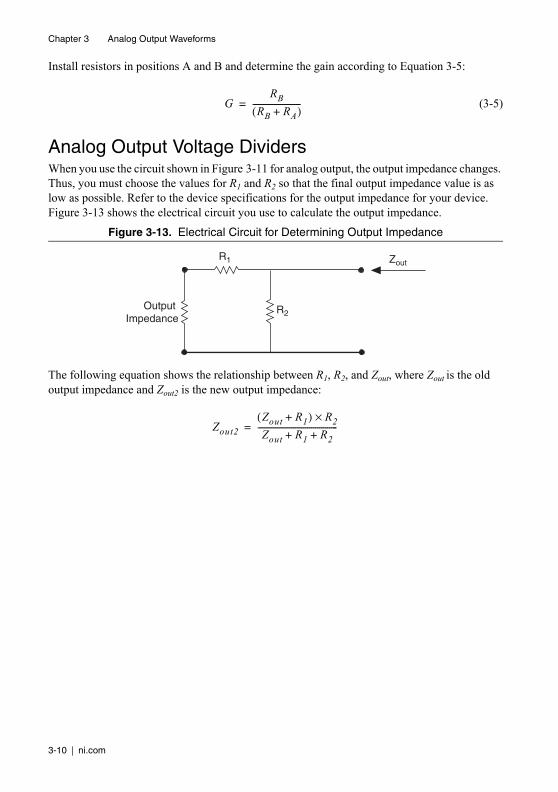
3-10 | ni.com
Chapter 3 Analog Output Waveforms
Install resistors in positions A and B and determine the gain according to Equation 3-5:
(3-5)
Analog Output Voltage DividersWhen you use the circuit shown in Figure 3-11 for analog output, the output impedance changes. Thus, you must choose the values for R1 and R2 so that the final output impedance value is as low as possible. Refer to the device specifications for the output impedance for your device. Figure 3-13 shows the electrical circuit you use to calculate the output impedance.
Figure 3-13. Electrical Circuit for Determining Output Impedance
The following equation shows the relationship between R1, R2, and Zout, where Zout is the old output impedance and Zout2 is the new output impedance:
GRB
RB RA+( )------------------------=
R2Output
Impedance
R1 Zout
Zout2
Zout R1+( ) R2×Zout R1 R2+ +
----------------------------------------=
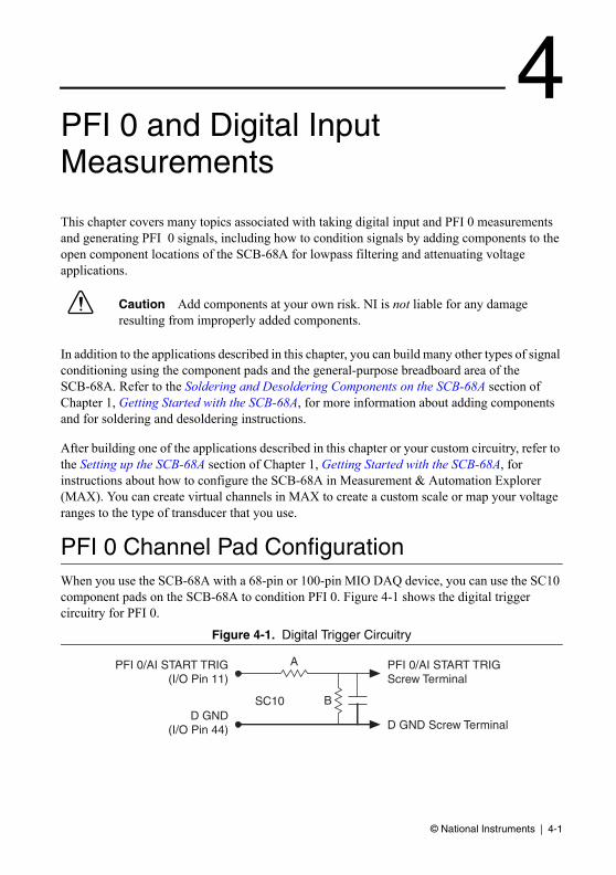
© National Instruments | 4-1
4PFI 0 and Digital Input Measurements
This chapter covers many topics associated with taking digital input and PFI 0 measurements and generating PFI 0 signals, including how to condition signals by adding components to the open component locations of the SCB-68A for lowpass filtering and attenuating voltage applications.
Caution Add components at your own risk. NI is not liable for any damage resulting from improperly added components.
In addition to the applications described in this chapter, you can build many other types of signal conditioning using the component pads and the general-purpose breadboard area of the SCB-68A. Refer to the Soldering and Desoldering Components on the SCB-68A section of Chapter 1, Getting Started with the SCB-68A, for more information about adding components and for soldering and desoldering instructions.
After building one of the applications described in this chapter or your custom circuitry, refer to the Setting up the SCB-68A section of Chapter 1, Getting Started with the SCB-68A, for instructions about how to configure the SCB-68A in Measurement & Automation Explorer (MAX). You can create virtual channels in MAX to create a custom scale or map your voltage ranges to the type of transducer that you use.
PFI 0 Channel Pad ConfigurationWhen you use the SCB-68A with a 68-pin or 100-pin MIO DAQ device, you can use the SC10 component pads on the SCB-68A to condition PFI 0. Figure 4-1 shows the digital trigger circuitry for PFI 0.
Figure 4-1. Digital Trigger Circuitry
B
PFI 0/AI START TRIG(I/O Pin 11)
A
D GND(I/O Pin 44)
PFI 0/AI START TRIGScrew Terminal
D GND Screw Terminal
SC10
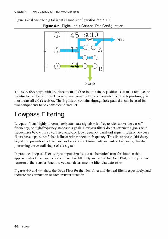
4-2 | ni.com
Chapter 4 PFI 0 and Digital Input Measurements
Figure 4-2 shows the digital input channel configuration for PFI 0.
Figure 4-2. Digital Input Channel Pad Configuration
The SCB-68A ships with a surface mount 0 Ω resistor in the A position. You must remove the resistor to use the position. If you remove your custom components from the A position, you must reinstall a 0 Ω resistor. The B position contains through hole pads that can be used for two components to be connected in parallel.
Lowpass FilteringLowpass filters highly or completely attenuate signals with frequencies above the cut-off frequency, or high-frequency stopband signals. Lowpass filters do not attenuate signals with frequencies below the cut-off frequency, or low-frequency passband signals. Ideally, lowpass filters have a phase shift that is linear with respect to frequency. This linear phase shift delays signal components of all frequencies by a constant time, independent of frequency, thereby preserving the overall shape of the signal.
In practice, lowpass filters subject input signals to a mathematical transfer function that approximates the characteristics of an ideal filter. By analyzing the Bode Plot, or the plot that represents the transfer function, you can determine the filter characteristics.
Figures 4-3 and 4-4 show the Bode Plots for the ideal filter and the real filter, respectively, and indicate the attenuation of each transfer function.
45
11
44
SC10
A+
B
11+
44
PFI 0
D GND

© National Instruments | 4-3
NI SCB-68A User Manual
Figure 4-3. Transfer Function Attenuation for an Ideal Filter
Figure 4-4. Transfer Function Attenuation for a Real Filter
The cut-off frequency, fc, is defined as the frequency beyond which the gain drops 3 dB. Figure 4-3 shows how an ideal filter causes the gain to drop to zero for all frequencies greater than fc. Thus, fc does not pass through the filter to its output. Instead of having a gain of absolute zero for frequencies greater than fc, the real filter has a transition region between the passband and the stopband, a ripple in the passband, and a stopband with a finite attenuation gain.
Real filters have some nonlinearity in their phase response, causing signals at higher frequencies to be delayed longer than signals at lower frequencies and resulting in an overall shape distortion of the signal. For example, when the square wave, shown in Figure 4-5, enters a filter, an ideal filter smooths the edges of the input, whereas a real filter causes some ringing in the signal as the higher frequency components of the signal are delayed.
Passband
Stopband
Log Frequency
Gai
n
fc
Passband
Stopband
Log Frequency
Gai
n
fc
TransitionRegion

4-4 | ni.com
Chapter 4 PFI 0 and Digital Input Measurements
Figure 4-5. Square Wave Input Signal
Figures 4-6 and 4-7 show the difference in response to a square wave between an ideal and a real filter, respectively.
Figure 4-6. Response of an Ideal Filter to a Square Wave Input Signal
Figure 4-7. Response of a Real Filter to a Square Wave Input Signal
Time (t)
Vol
ts (
V)
Time (t)
Vol
ts (
V)
Time (t)
Vol
ts (
V)
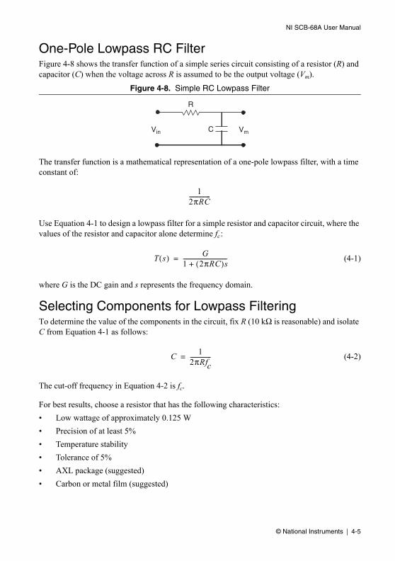
© National Instruments | 4-5
NI SCB-68A User Manual
One-Pole Lowpass RC FilterFigure 4-8 shows the transfer function of a simple series circuit consisting of a resistor (R) and capacitor (C) when the voltage across R is assumed to be the output voltage (Vm).
Figure 4-8. Simple RC Lowpass Filter
The transfer function is a mathematical representation of a one-pole lowpass filter, with a time constant of:
Use Equation 4-1 to design a lowpass filter for a simple resistor and capacitor circuit, where the values of the resistor and capacitor alone determine fc:
(4-1)
where G is the DC gain and s represents the frequency domain.
Selecting Components for Lowpass FilteringTo determine the value of the components in the circuit, fix R (10 kΩ is reasonable) and isolate C from Equation 4-1 as follows:
(4-2)
The cut-off frequency in Equation 4-2 is fc.
For best results, choose a resistor that has the following characteristics:
• Low wattage of approximately 0.125 W
• Precision of at least 5%
• Temperature stability
• Tolerance of 5%
• AXL package (suggested)
• Carbon or metal film (suggested)
R
CVin Vm
12πRC---------------
T s( ) G1 2πRC( )s+-------------------------------=
C1
2πRfc---------------=

4-6 | ni.com
Chapter 4 PFI 0 and Digital Input Measurements
Choose a capacitor that has the following suggested characteristics:
• AXL or RDL package
• Tolerance of 20%
• Maximum voltage of at least 25 V
Adding Components for Lowpass Digital Filtering on Digital Trigger Input SignalsUsing the circuit shown in Figure 4-8, you can use a two-component circuit to build a simple RC filter with digital input. For PFI 0, add the resistor to position A and the capacitor to position B. Refer to Figure 4-9 for the digital input channel pad configuration.
The SCB-68A ships with a surface mount 0 Ω resistor in the A position. You must remove the resistor to use the position.
Figure 4-9. SCB-68A Circuit Diagram for Digital Trigger Input Lowpass Filter
45
11
44
SC10
A+
B
11+
44
PFI 0
D GND
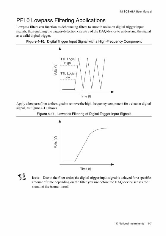
© National Instruments | 4-7
NI SCB-68A User Manual
PFI 0 Lowpass Filtering ApplicationsLowpass filters can function as debouncing filters to smooth noise on digital trigger input signals, thus enabling the trigger-detection circuitry of the DAQ device to understand the signal as a valid digital trigger.
Figure 4-10. Digital Trigger Input Signal with a High-Frequency Component
Apply a lowpass filter to the signal to remove the high-frequency component for a cleaner digital signal, as Figure 4-11 shows.
Figure 4-11. Lowpass Filtering of Digital Trigger Input Signals
Note Due to the filter order, the digital trigger input signal is delayed for a specific amount of time depending on the filter you use before the DAQ device senses the signal at the trigger input.
Time (t)
Vol
ts (
V)
TTL LogicHigh
TTL LogicLow
Time (t)
Vol
ts (
V)

4-8 | ni.com
Chapter 4 PFI 0 and Digital Input Measurements
Attenuating VoltageTransducers can generate more than 10 VDC per channel, but DAQ devices cannot read more than 10 VDC per input channel. Therefore, you must attenuate output signals from the transducer to fit within the DAQ device specifications. Figure 4-12 shows how to use a voltage divider to attenuate the output signal of the transducer.
Figure 4-12. Attenuating Voltage with a Voltage Divider
The voltage divider splits the input voltage (Vin) between two resistors (R1 and R2), causing the voltage on each resistor to be noticeably lower than Vin. Use Equation 4-3 to determine the Vm that the DAQ device measures:
(4-3)
Use Equation 4-4 to determine the overall gain of a voltage divider circuit:
(4-4)
The accuracy of Equation 4-4 depends on the tolerances of the resistors that you use.
Caution The SCB-68A is not designed for any input voltages >30 Vrms/42 Vpk/60 VDC, even if a user-installed voltage divider reduces the voltage to within the input range of the DAQ device. Input voltages >30 Vrms/42 Vpk/60 VDC can damage the SCB-68A, any devices connected to it, and the host computer. Overvoltage can also cause an electric shock hazard for the operator.
R2Vin Vm
+
–
+
–
R1
Vm Vin
R2
R1 R2+------------------ =
GVm
Vin-------
R2
R1 R2+------------------= =

© National Instruments | 4-9
NI SCB-68A User Manual
Selecting Components for Attenuating VoltageTo set up the resistors, complete the following steps.
1. Select the value for R2 (10 kΩ is recommended).
2. Use Equation 4-3 to calculate the value for R1.
Base the R1 calculation on the following values:
• Maximum Vin you expect from the transducer
• Maximum voltage (<10 VDC) that you want to input to the DAQ device
Accuracy Considerations for Attenuating VoltageFor best results when attenuating voltage, choose a resistor that has the following characteristics:
• Low wattage of approximately 0.125 W
• Precision of at least 5%
• Temperature stable
• Tolerance of 5%
• AXL package (suggested)
• Carbon or metal film (suggested)
Verify that R1 and R2 drift together with respect to temperature; otherwise, the system may consistently read incorrect values.
Adding Components for Attenuating Voltage on Digital InputsTo build a two-resistor circuit for attenuating voltages at the PFI 0 pin on the SCB-68A, refer to the pad positions in Figure 4-13.
The SCB-68A ships with a surface mount 0 Ω resistor in the SC10 position. You must remove the resistor to use the position.

4-10 | ni.com
Chapter 4 PFI 0 and Digital Input Measurements
Figure 4-13. SCB-68A Circuit Diagram for Digital Input Attenuation
Use positions A and B for PFI 0, and determine the gain according to Equation 4-5:
(4-5)
Digital Input Voltage DividersIf you use the Vin voltage of Figure 4-12 to feed TTL signals, you must calculate Vin so that the voltage drop on R2 does not exceed 5 V.
Caution A voltage drop exceeding 5 V on R2 can damage the internal circuitry of the DAQ device. NI is not liable for any device damage resulting from improper use of the SCB-68A and the DAQ device.
45
11
44
SC10
A+
B
11+
44
PFI 0
D GND
GB
B A+( )------------------=

© National Instruments | 5-1
5Fuse and Power Information
Refer to the Soldering and Desoldering Components on the SCB-68A section of Chapter 1, Getting Started with the SCB-68A, for more information about adding components and for soldering and desoldering instructions.
Power Supply CircuitryFigure 5-1 shows the power supply circuitry on the SCB-68A.
Figure 5-1. +5 V Power Supply
FuseSome DAQ devices provide +5 V power on pin 8 and pin 14. Pin 8 from the DAQ device is protected by a 1 A self-resetting fuse, shown in Figure 1-2, SCB-68A Printed Circuit Board Diagram. Shorting pin 8 to ground trips the fuse on the SCB-68A. Pin 14 is not fuse-protected on the SCB-68A. Shorting pin 14 will cause the fuse on the DAQ device to open.
If the SCB-68A does not work when you power on the DAQ device, check the switch settings on the SCB-68A and the output fuse (if any) on the DAQ device.
+5 V(I/O Pin 8)
+5 V Screw Terminal
ACC Not Powered (NC)
C2(10 μF)
F11 A
S2.2ACC Powered
C1(0.1 μF)
R20(Optional)
R21
C6(10 μF)
C4(0.1 μF)
+5 V
Non-MIO(NC)
MIO
D GND(I/O Pin 7)
D GNDScrew Terminal
Non-MIO(NC)
MIO
AI GND(I/O Pin 56)
AI GNDScrew Terminal
AIAI
AI
S2.3
S2.1

5-2 | ni.com
Chapter 5 Fuse and Power Information
Adding Power Filters
Caution If you are modifying the power filter, do not draw ≥100 mA from the +5 V power line.
A 470 Ω series resistor (R21) is part of the power filter for the +5 V power on the SCB-68A. Due to the nature of the filter design, as the filtered +5 V is loaded, the voltage supplied to the SCB-68A circuitry and screw terminal 8 decreases. Pad R20, shown in Figure 1-2, SCB-68A Printed Circuit Board Diagram, is in parallel with R21. You can install a resistor, if needed, to decrease the overall resistance used in the filter and reduce the loading effect. However, completely shorting R20 bypasses the filter while capacitively coupling D GND to AI GND and AO GND and is not recommended.
Caution Add components at your own risk. NI is not liable for any damage resulting from improperly added components.
Caution NI is not liable for any device damage resulting from improper use of the SCB-68A and the DAQ device.

© National Instruments | A-1
ASpecifications
This appendix lists the SCB-68A specifications. These specifications are typical at 25 °C unless otherwise noted.
Caution Do not connect hazardous voltages (>30 Vrms/42 Vpk/60 VDC) to the SCB-68A.
Temperature SensorAccuracy........................................................... ±1.0 °C over a 0 to 70 °C range
Power RequirementPower consumption (at +5 VDC, ±5%)
Typical ...................................................... 1 mA with no signal conditioning installedMaximum.................................................. 800 mA from host computer
Note The power specifications pertain to the power supply of the host computer when using internal power or to the external supply connected at the +5 V screw terminal when using external power. The maximum power consumption of the SCB-68A is a function of the signal conditioning components installed and any circuits constructed on the general-purpose breadboard area. If the SCB-68A is powered from the host computer, the maximum +5 V current draw, which is limited by the fuse, is 800 mA.
FuseRating................................................................ 1.10 A, 8 VDC SMT PTC
Fuse is not user-replaceable
Physical CharacteristicsDimensions (including feet) ............................. 14.7 × 14.7 × 3.0 cm (5.8 × 5.8 × 1.2 in.)
Weight............................................................... 644 g (1 lb 7 oz)
I/O connector .................................................... One 68-pin male SCSI connector
Screw terminals ................................................ 68, all I/O signals are available at screw terminals
Wire gauge................................................ 14–30 AWGTorque ....................................................... 0.5–0.6 N ⋅ m (4.4–5.3 in. ⋅ lb)
Through hole pads ............................................ 0.8 to 0.9 mm (in diameter)

A-2 | ni.com
Appendix A Specifications
Safety VoltagesConnect only voltages that are no greater than 30 Vrms/42 Vpk/60 VDC.
EnvironmentalTemperature
Operating ..................................................0 to 70 °CStorage ......................................................–20 to 70 °C
Relative humidityOperating ..................................................5 to 90% RH, noncondensingStorage ......................................................5 to 90% RH, noncondensing
Pollution Degree ...............................................2
Maximum altitude.............................................2,000 m
Indoor use only.
SafetyThis product meets the requirements of the following standards of safety for electrical equipment for measurement, control, and laboratory use:
• IEC 61010-1, EN 61010-1
• UL 61010-1, CSA 61010-1
Note For UL and other safety certifications, refer to the product label or the Online Product Certification section.
Electromagnetic CompatibilityThis product meets the requirements of the following EMC standards for electrical equipment for measurement, control, and laboratory use:
• EN 61326-1 (IEC 61326-1): Class A emissions; Basic immunity
• EN 55011 (CISPR 11): Group 1, Class A emissions
• AS/NZS CISPR 11: Group 1, Class A emissions
• FCC 47 CFR Part 15B: Class A emissions
• ICES-001: Class A emissions
Note In the United States (per FCC 47 CFR), Class A equipment is intended for use in commercial, light-industrial, and heavy-industrial locations. In Europe, Canada, Australia and New Zealand (per CISPR 11) Class A equipment is intended for use only in heavy-industrial locations.
Note Group 1 equipment (per CISPR 11) is any industrial, scientific, or medical equipment that does not intentionally generate radio frequency energy for the treatment of material or inspection/analysis purposes.

© National Instruments | A-3
NI SCB-68A User Manual
Note For EMC declarations and certifications, and additional information, refer to the Online Product Certification section.
CE ComplianceThis product meets the essential requirements of applicable European Directives as follows:
• 2006/95/EC; Low-Voltage Directive (safety)
• 2004/108/EC; Electromagnetic Compatibility Directive (EMC)
Online Product CertificationRefer to the product Declaration of Conformity (DoC) for additional regulatory compliance information. To obtain product certifications and the DoC for this product, visit ni.com/certification, search by model number or product line, and click the appropriate link in the Certification column.
Environmental ManagementNI is committed to designing and manufacturing products in an environmentally responsible manner. NI recognizes that eliminating certain hazardous substances from our products is beneficial to the environment and to NI customers.
For additional environmental information, refer to the NI and the Environment Web page at ni.com/environment. This page contains the environmental regulations and directives with which NI complies, as well as other environmental information not included in this document.
Waste Electrical and Electronic Equipment (WEEE)EU Customers At the end of the product life cycle, all products must be sent to a WEEE recycling center. For more information about WEEE recycling centers, National Instruments WEEE initiatives, and compliance with WEEE Directive 2002/96/EC on Waste and Electronic Equipment, visit ni.com/environment/weee.
RoHSNational Instruments
(RoHS) National Instruments RoHS ni.com/environment/rohs_china (For information about China RoHS compliance, go to ni.com/environment/rohs_china.)

© National Instruments | B-1
BTechnical Support and Professional Services
Log in to your National Instruments ni.com User Profile to get personalized access to your services. Visit the following sections of ni.com for technical support and professional services:
• Support—Technical support at ni.com/support includes the following resources:
– Self-Help Technical Resources—For answers and solutions, visit ni.com/support for software drivers and updates, a searchable KnowledgeBase, product manuals, step-by-step troubleshooting wizards, thousands of example programs, tutorials, application notes, instrument drivers, and so on. Registered users also receive access to the NI Discussion Forums at ni.com/forums. NI Applications Engineers make sure every question submitted online receives an answer.
– Standard Service Program Membership—This program entitles members to direct access to NI Applications Engineers via phone and email for one-to-one technical support, as well as exclusive access to self-paced online training modules at ni.com/self-paced-training. All customers automatically receive a one-year membership in the Standard Service Program (SSP) with the purchase of most software products and bundles including NI Developer Suite. NI also offers flexible extended contract options that guarantee your SSP benefits are available without interruption for as long as you need them. Visit ni.com/ssp for more information.
– For information about other technical support options in your area, visit ni.com/services, or contact your local office at ni.com/contact.
• Training and Certification—Visit ni.com/training for training and certification program information. You can also register for instructor-led, hands-on courses at locations around the world.
• System Integration—If you have time constraints, limited in-house technical resources, or other project challenges, National Instruments Alliance Partner members can help. To learn more, call your local NI office or visit ni.com/alliance.
• Declaration of Conformity (DoC)—A DoC is our claim of compliance with the Council of the European Communities using the manufacturer’s declaration of conformity. This system affords the user protection for electromagnetic compatibility (EMC) and product safety. You can obtain the DoC for your product by visiting ni.com/certification.
• Calibration Certificate—If your product supports calibration, you can obtain the calibration certificate for your product at ni.com/calibration.

B-2 | ni.com
Appendix B Technical Support and Professional Services
You also can visit the Worldwide Offices section of ni.com/niglobal to access the branch office Web sites, which provide up-to-date contact information, support phone numbers, email addresses, and current events.

© National Instruments | I-1
Index
Numerics+5 V signal
adding power filters, 5-2power supply (figure), 5-1
Aaccuracy considerations for attenuating
voltage, 2-36, 3-9, 4-9adding
components, 4-1, 5-1channel pad configurations, 2-20,
4-2power filters, 5-2
analog inputattenuating voltage, 2-37
differential, 2-37single-ended, 2-37
bias resistors, 2-20balanced, 2-20single, 2-20
channel pad configuration, 2-2circuit diagram (figure), 2-2component locations (table), 2-5connecting signals, 2-5current input measurement, 2-33
differential, 2-33single-ended, 2-34
highpass filtering, 2-30applications, 2-31differential, 2-30single-ended, 2-30
lowpass filtering, 2-25applications, 2-26differential, 2-25single-ended, 2-25
open thermocouple detectiondifferential, 2-18single-ended, 2-19
thermocouple input filtering, 2-19voltage dividers, 2-38
analog outputattenuating voltage, 3-9channel pad configurations, 2-5circuit diagram (figure), 3-1component locations (table), 3-2lowpass filtering
applications, 3-7smoothing filters, 3-6
voltage dividers, 3-10attenuating voltage, 2-35, 3-8, 4-8
accuracy considerations, 2-36, 3-9, 4-9analog input, 2-37
differential, 2-37single-ended, 2-37
analog output, 3-9components
adding, 2-37, 3-9, 4-9selecting, 2-36, 3-9, 4-9
digital inputs, 4-9PFI 0, 4-9voltage dividers, 3-10
Bbias resistors, 2-20
balanced, 2-20single, 2-20
Ccalibration certificate (NI resources), B-1channel pad configuration
analog input, 2-2analog output, 2-5
circuit diagrams+5 V power supply (figure), 5-1analog input (figure), 2-2analog output (figure), 3-1cold-junction compensation (figure), 2-2digital inputs (figure), 4-1digital trigger (figure), 4-1PFI 0 (figure), 4-1
cold-junction compensation (CJC) circuit diagram (figure), 2-2
Index
I-2 | ni.com
componentsadding
attenuating voltage, 2-37, 3-9, 4-9current input measurement, 2-33highpass filtering, 2-30lowpass filtering, 2-25, 3-6, 4-6
locationsanalog input (table), 2-5analog output (table), 3-2
selectingattenuating voltage, 2-36, 3-9, 4-9current input measurement, 2-33highpass filtering, 2-29lowpass filtering, 2-24, 3-6, 4-5
connectionsanalog input signals, 2-5differential for floating signal
sources, 2-12floating signal sources, 2-7ground-referenced signal sources, 2-12single-ended for floating signal
sources, 2-12single-ended, RSE configuration, 2-12
conventions used in the manual, vcurrent input measurement, 2-32
adding components, 2-33analog input, 2-33
differential, 2-33single-ended, 2-34
selecting a resistor, 2-33
DDeclaration of Conformity
(NI resources), B-1diagnostic tools (NI resources), B-1differential connections
bias resistorsbalanced, 2-20single, 2-20
current input measurement, 2-33highpass filtering, 2-30lowpass filtering, 2-25open thermocouple detection, 2-18using with floating signal sources, 2-8
using with ground-referenced signal sources, 2-14
when to use with floating signal sources, 2-7
when to use with ground-referenced signal sources, 2-12
digital inputsattenuating voltage, 4-9circuit diagram (figure), 4-1lowpass filtering
applications, 4-7voltage dividers, 4-10
digital triggerscircuit diagram (figure), 4-1lowpass filtering
applications, 4-7documentation, 1-13
conventions used in the manual, vNI resources, B-1
drivers (NI resources), B-1
Eexamples (NI resources), B-1
Ffiltering
highpass, 2-27, 4-8lowpass, 2-21, 3-2, 4-2power, 5-2thermocouple input, 2-19
floating signal sourcesconnecting, 2-7description, 2-7using in differential mode, 2-8using in NRSE mode, 2-11using in RSE mode, 2-12when to use
in differential mode, 2-7in NRSE mode, 2-7in RSE mode, 2-8

NI SCB-68A User Manual
© National Instruments | I-3
Gground-referenced signal sources
connecting, 2-12description, 2-12using in differential mode, 2-14using in NRSE mode, 2-15when to use in differential mode, 2-12when to use in NRSE mode, 2-13when to use in RSE mode, 2-13
Hhelp, technical support, B-1highpass filtering, 2-27, 4-8
analog input, 2-30applications, 2-31differential, 2-30single-ended, 2-30
componentsadding, 2-30selecting, 2-29
one-pole highpass RC filter, 2-29
Iinstalling bias resistors, 2-20instrument drivers (NI resources), B-1
KKnowledgeBase, B-1
Llowpass filtering, 2-21, 3-2, 4-2
analog input, 2-25differential, 2-25single-ended, 2-25
analog output, 3-6applications
analog input, 2-26analog output, 3-7digital inputs, 4-7digital triggers, 4-7PFI 0, 4-7
componentsadding for analog input, 2-25adding for analog output, 3-6adding for digital filtering, 4-6selecting, 2-24, 3-6, 4-5
one-pole lowpass RC filter, 2-24, 3-5, 4-5
Mmeasurement
current inputanalog input, 2-32analog output, 3-8digital input, 4-8
NNational Instruments support and
services, B-1non-referenced single-ended connections
using with floating signal sources, 2-11using with ground-referenced signal
sources, 2-15when to use with floating signal
sources, 2-7when to use with ground-referenced
signal sources, 2-13
Oone-pole
highpass RC filter, 2-29lowpass RC filter
analog input, 2-24analog output, 3-5digital trigger, 4-5
open thermocouple detection, 2-18sources of error, 2-19
PPFI 0, 4-1
attenuating voltage, 4-9circuit diagram (figure), 4-1lowpass filtering applications, 4-7

Index
I-4 | ni.com
power filters, 5-2printed circuit board diagram (figure), 1-4programming examples (NI resources), B-1
Rreferenced single-ended connections
using with floating signal sources, 2-12when to use with floating signal
sources, 2-8when to use with ground-referenced
signal sources, 2-13related documentation, 1-13removing the SCB-68 board from the
base, 1-11
Ssignals
connecting analog input, 2-5floating sources, 2-7ground-referenced, 2-12
single bias resistor, 2-20single-ended connections
attenuating voltage, 2-37current input measurement, 2-34for floating signal sources, 2-12highpass filtering, 2-30lowpass filtering, 2-25open thermocouple detection, 2-19RSE configuration, 2-12when to use non-referenced single-ended
connections with floating signal sources, 2-7
when to use referenced single-ended connections with floating signal sources, 2-8
software (NI resources), B-1soldering and desoldering
equipment, 1-11guidelines, 1-12
sources of error, open thermocouple detection, 2-19
specifications, A-1support, technical, B-1
Ttechnical support, B-1temperature sensor
accuracy, 2-17output, 2-17
thermocouples, 2-21, 4-2input filtering, 2-19open thermocouple detection, 2-18
differential analog input, 2-18single-ended analog input, 2-19sources of error, 2-19
temperature sensor output and accuracy, 2-17
training and certification (NI resources), B-1troubleshooting (NI resources), B-1
Vvoltage attenuation
analog input, 2-35analog output, 3-8digital input, 4-8voltage dividers, 3-10
voltage dividers, 3-10analog input, 2-38analog output, 3-10digital inputs, 4-10
WWeb resources, B-1