a 3d data transformation processor dimitrios megas, kleber pizolato, timothy levin, and ted huffmire...
TRANSCRIPT

A 3D Data Transformation Processor
Dimitrios Megas, Kleber Pizolato, Timothy Levin, and Ted Huffmire
WESS 2012October 11, 2012

Disclaimer
• The views presented in this talk are those of the speaker and do not necessarily reflect the views of the United States Department of Defense or the National Science Foundation.

Split Manufacturing
• Face-to-Back (F2B) Bonding
Basic Idea
• Combine using 3D integration:– Processor– Compression coprocessor– Cryptographic coprocessor

Basic Idea
• CPU Layer + Coprocessor Layer

Basic Idea
• Real-time trace collection– Compress trace prior to transmission to off-chip
storage for offline program analysis• Optional encryption step can protect the compressed data
from interception
– High-performance stand-alone encryption service– XTRec: Secure Real-time Execution Trace Recording on
Commodity Platforms (CMU)– Trusted computing: mitigate glitch attack against TPM
(runtime hash of memory, capture sequence of instructions executed)

Basic Idea
• Real-time trace collection– The amount of data collected depends on the
granularity of the collection and the speed of the system
– Monitoring and collecting more signals results in a larger data stream

Outline
• Motivation and Background• Design Goals• Design Choices• System Architecture• Conclusions and Future Work

Outline
• Motivation and Background• Design Goals• Design Choices• System Architecture• Conclusions and Future Work

Cryptographic Coprocessing
• 3D vs. 2D

Medical Image Processing
• [Cong 2011]

3D-MAPS V1 vs V2
• Georgia Tech [Kim et al., ISSCC 2012]3D-MAPS V1 3D-MAPS V2
# of tiers 2 (1 logic, 1 SRAM) 5 (2 logic, 3 DRAM)
# of cores 64 128Memory capacity 256KB SRAM 256MB DRAM & 512KB SRAM
Logic footprint 5mm X 5mm 10mm X 10mm
DRAM footprint - 20mm X 12mm
Bonding style F2F F2F and F2B
TSV/F2F usage ~ 50K / ~50K ~ 150K / ~185K
Memory access* 2048 bit/cycle SRAM 1024 bit/cycle DRAM
freq / power 277MHz / 4.0W 175MHz / 10.4W
* Wide-I/O allows 512 bit/cycle DRAM access

Stack Up Comparison
• TSV usage– 3D-MAPS V1: For I/O (204 redundancy)– 3D-MAPS V2: For I/O (204 redundancy) and DRAM
access (9 redundancy)

What is 3Dsec?
• Economics of High Assurance– High NRE Cost, Low Volume– Gap between DoD and Commercial
• Disentangle security from the COTS– Use a separate chip for security– Use 3-D Integration to combine:
• Control Plane• Computation Plane
– Need to add posts to the COTS chip design• Dual use of computation plane

Pro’s and Con’s
• Why not use a co-processor? On-chip?• Pro’s
– High bandwidth and low latency– Controlled lineage– Direct access to internal structures
• Con’s– Thermal and cooling– Design and testing– Manufacturing yield

Cost
• Cost of fabricating systems with 3-D– Fabricating and testing the security layer– Bonding it to the host layer– Fabricating the vias– Testing the joined unit
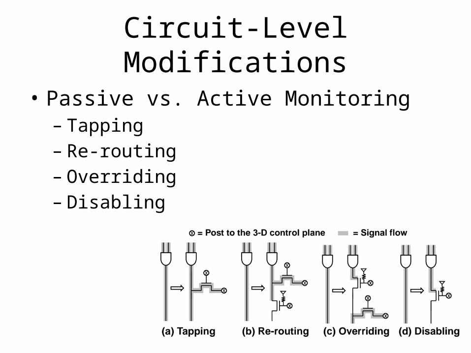
Circuit-Level Modifications
• Passive vs. Active Monitoring– Tapping– Re-routing– Overriding– Disabling
3-D Application Classes
• Enhancement of native functions• Secure alternate service• Isolation and protection• Passive monitoring
– Information flow tracking– Runtime correctness checks– Runtime security auditing

Outline
• Motivation and Background• Design Goals• Design Choices• System Architecture• Conclusions and Future Work

Design Goals
• High Performance• Ability to gather and compress architectural
state of a processor at runtime

Outline
• Motivation and Background• Design Goals• Design Choices• System Architecture• Conclusions and Future Work

Design Choices
• Manufacturing process– Face-to-face (F2F)
• Compression algorithm/hw– Two stages: filtering + general-purpose
• Crypto algorithm/hw– AES-128, SHA-1, SHA-512
• Interface between planes– 128 F2F vias up, 32 down (direct connection)

Design Choices
• Other Issues– Coordination between planes
• Control words in special registers
– Interface within control plane• Output of compression input of crypto
– Delivery of I/O and power• Use existing capability of computation plane
– Computation plane hardware• High-performance general-purpose processor
– Clock synchronization• Tree network

Compression Study
• Use TCgen to compress a set of trace files generated using Pin– Traces capture memory access behavior of various
Linux applications• Vary parameters of TCgen for each field
– TCgen is prediction-based compression– Which algorithm is most effective?
• Apply general-purpose compression in second stage (gzip)

Trace Files (generated by Pin)• Instruction• Count PC ADDRESS Size• 8 0x52d70b 0x5913c000 4• 25 0x543cc6 0xbff10254 4• 25 0x543cc7 0xbff10258 4• 33 0x52d6bb 0xbff1025c 4• 33 0x52d6be 0xbff10260 4• 33 0x52d6c2 0xbff10264 4• 33 0x52d6c8 0xbff10268 4• 33 0x52d6c9 0xbff1026c 4• 37 0x9bcb44 0xa1a50800 4• 40 0x6eb126 0xbff10268 4
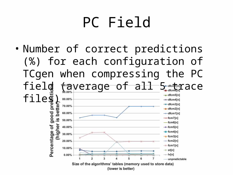
PC Field
• Number of correct predictions (%) for each configuration of TCgen when compressing the PC field (average of all 5 trace files)

Data Address Field
• Number of correct predictions (%) for each configuration of TCgen when compressing address field (average of all 5 trace files)

PC Field
• Compression ratio for the PC field
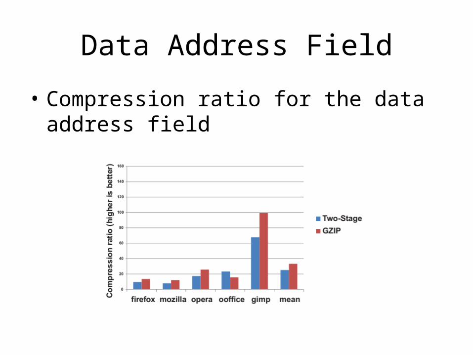
Data Address Field
• Compression ratio for the data address field

Outline
• Motivation and Background• Design Goals• Design Choices• System Architecture• Conclusions and Future Work

Computation Plane
• CPU

Control Plane
• Compression coprocessor (DFCM + gzip)

Control Plane
• gzip unit (within compression coprocessor)

Control Plane
• AES/SHA

Control Plane
• Microprocessor interface unit

Full 3D System
• 3D IC

Outline
• Motivation and Background• Design Goals• Design Choices• System Architecture• Conclusions and Future Work

Conclusions
• Applications: trusted computing, reverse engineering of malicious software, post-mortem analysis of system that has suffered an attack
• Simple preprocessing can decrease bandwidth (also gives power advantages)
• There is much to do before making silicon. It is useful to quantify the high-level tradeoffs:– Data to compress– Sampling rate– Number of TSVs– Throughput

Future Work
• Independent I/O and power delivery– How to share the I/O of computation plane?
• Floor Planning– How much logic/memory can you fit between the TSVs?
• It would be helpful for the 3D chip to be pin-compatible with the 2D package.– Use a network/share the TSVs?
• Joining dissimilar technology nodes– Use buffers, redundant hardware

Future Work• More types of trace files
– General-purpose interface, migration path– Can you test/verify computation plane without knowing what the control plane will
be?– Characteristics of a “typical” trace file?
• Hierarchy of compression, for power not just for compression ratio?– Lossy compression?!
• Trust issues– Who generates the write signal?– How to protect the key?– Can monitored software turn off monitoring?
• Hardware implementation– Simulation– FPGA prototype– Tape-out

Split Manufacturing
• Discussion Points– Can we trust the result of split manufacturing?– Could this approach harm security?– Is it worth it? When is it worth it?– Why not use trusted foundry always?– Are trusted foundries a band aid solution to offshoring
trend?– How to trust trusted foundry?– Why not use redundancy with majority vote?– Can we do everything from scratch?

Split Manufacturing
• Discussion Points– How to raise alarm if network interface is
controlled by adversary?• Use challenge-response protocols?
– Security architecture• Packaging considerations
• Distributed posts, policy state?• If computation plane can perform AES, why
perform AES in control plane?

Questions?
• faculty.nps.edu/tdhuffmi