a 5-6 ghz silicon-germanium vco with tunable polyphase outputs · 2020-01-22 ·...
TRANSCRIPT

A 5-6 GHz Silicon-Germanium VCO with TunablePolyphase Outputs
David I. Sanderson
Thesis submitted to the Faculty of the
Virginia Polytechnic Institute and State University
in partial fulfillment of the requirements for the degree of
Masters of Science
in
Electrical Engineering
Sanjay Raman, Chair
Charles W. Bostian
Joseph G. Tront
May 8, 2003
Blacksburg, Virginia
Keywords: 5 GHz, IEEE 802.11a, integrated circuit, oscillator, RFIC, SiGe, tunable
polyphase filter, U-NII, VCO, Weaver architecture, WLAN
Copyright 2003, David I. Sanderson

A 5-6 GHz Silicon-Germanium VCO with TunablePolyphase Outputs
David I. Sanderson
(ABSTRACT)
In-phase and quadrature (I/Q) signal generation is often required in modern trans-
ceiver architectures, such as direct conversion or low-IF, either for vector modulation
and demodulation, negative frequency recovery in direct conversion receivers, or im-
age rejection. If imbalance between the I and Q channels exists, the bit-error-rate
(BER) of the transceiver and/or the image rejection ratio (IRR) will quickly deterio-
rate. Methods for correcting I/Q imbalance are desirable and necessary to improve
the performance of quadrature transceiver architectures and modulation schemes.
This thesis presents the design and characterization of a monolithic 5-6 GHz Silicon
Germanium (SiGe) inductor-capacitor (LC ) tank voltage controlled oscillator (VCO)
with tunable polyphase outputs. Circuits were designed and fabricated using the
Motorola 0.4 µm CDR1 SiGe BiCMOS process, which has four interconnect metal
layers and a thick copper uppermost bump layer for high-quality radio frequency (RF)
passives.
The VCO design includes full-wave electromagnetic characterization of an electrically
symmetric differential inductor and a traditional dual inductor. Differential effective
inductance and Q factor are extracted and compared for simulated and measured
inductors. At 5.25 GHz, the measured Q factors of the electrically symmetric and
dual inductors are 15.4 and 10.4, respectively. The electrically symmetric inductor
provides a measured 48% percent improvement in Q factor over the traditional dual
inductor.
Two VCOs were designed and fabricated; one uses the electrically symmetric inductor
in the LC tank circuit while the other uses the dual inductor. Both VCOs are based
on an identical cross-coupled, differential pair negative transconductance (−GM) os-
cillator topology. Analysis and design considerations of this topology are presented
with a particular emphasis on designing for low phase noise and low-power consump-
tion. The fabricated VCO with an electrically symmetric inductor in the tank circuit

tunes from 4.19 to 5.45 GHz (26% tuning range) for control voltages from 1.7 to 4.0
V. This circuit consumes 3.81 mA from a 3.3 V supply for the VCO core and 14.1
mA from a 2.5 V supply for the output buffer. The measured phase noise is −115.5dBc/Hz at a 1 MHz offset and a tank varactor control voltage of 1.0 V. The VCO
figure-of-merit (FOM) for the symmetric inductor VCO is −179.2 dBc/Hz, which iswithin 4 dBc/Hz of the best reported VCO in the 5 GHz frequency regime. The
die area including pads for the symmetric inductor VCO is 1 mm × 0.76 mm. In
comparison, the dual inductor VCO tunes from 3.50 to 4.58 GHz (27% tuning range)
for control voltages from 1.7 to 4.0 V. DC power consumption of this circuit consists
of 3.75 mA from a 3.3 V supply for the VCO and 13.3 mA from a 2.5 V supply for
the buffer. At 1 MHz from the carrier and a control voltage of 0 V, the dual inductor
VCO has a phase noise of −104 dBc/Hz. The advantage of the higher Q symmetric
inductor is apparent by comparing the FOM of the two VCO designs at the same var-
actor control voltage of 0 V. At this tuning voltage, the dual inductor VCO FOM is
−166.3 dBc/Hz compared to −175.7 dBc/Hz for the symmetric inductor VCO – an
improvement of about 10 dBc/Hz. The die area including pads for the dual inductor
VCO is 1.2 mm × 0.76 mm.In addition to these VCOs, a tunable polyphase filter with integrated input and output
buffers was designed and fabricated for a bandwidth of 5.15 to 5.825 GHz. Series
tunable capacitors (varactors) provide phase tunability for the quadrature outputs of
the polyphase filter. The die area of the tunable polyphase with pads is 920 µm ×755 µm. The stand-alone polyphase filter consumes 13.74 mA in the input buffer
and 6.29 mA in the two output buffers from a 2.5 V supply. Based on measurements,
approximately 15 of I/Q phase imbalance can be tuned out using the fabricated
polyphase filter, proving the concept of tunable phase. The output varactor control
voltages can be used to achieve a potential ±5 phase flatness bandwidth of 700 MHz.To the author’s knowledge, this is the first reported I/Q balance tunable polyphase
network.
The tunable polyphase filter can be integrated with the VCO designs described above
to yield a quadrature VCO with phase tunable outputs. Based on the above designs
I/Q tunability can be added to VCO at the expense of about 6 mA. Future work
includes testing of a fabricated version of this combined polyphase VCO circuit.
iii

Acknowledgment
I would like to thank Dr. Sanjay Raman, my advisor, for working with me over
the past couple of years. He provides an ideal research environment for students to
simultaneously learn and contribute to the continually advancing field of RF micro-
electronics. I am also grateful for the time my other committee advisors, Dr. Charles
W. Bostian and Dr. Joseph G. Tront, spent reviewing this thesis.
This work was fabricated using the Motorola 0.4 µmCDR1 SiGe BiCMOS process. A
special thank you needs to be extended to Eric Maass, of Motorola SPS, for providing
access to both this process and the help of the Motorolans who support CDR1. In
particular, Karen Dotson for help in preparation for tape out, Brian Kump for help
with a few puzzling DRC and LVS errors, and Francisco Chico Yanez for help with
the layout and fabrication of the test boards. Bruce Smith, also of Motorola SPS,
deserves a special thanks for his support, diligence, and extreme patience throughout
the whole fabrication and packaging process.
I would like to thank Shawn Bowers of Amkor Technologies for his assistance in
packaging the fabricated circuits.
I am grateful to Shawn Carpenter of Sonnet Software for the donation of a beta
version of Sonnet I used for the full-wave electromagnetic simulation of monolithic
inductors. I would also like to thank Gregory Kinnetz, also of Sonnet Software, who
provided a feedback path for the beta testing. Revisions to the em solver meshing
schemes during this research made the numerous simulations of this thesis possible.
A Cascade Microprobe station was used to measure the monolithic inductors for this
work. I would like to thank Linda Jaffe, Ken Matheson, and Tariq Alam of Cascade
Microtech for their help with calibration procedures for the probe station.
iv

I would like to thank Ryan Bunch of RF Micro Devices for providing access to the
Agilent E5500 and for his assistance with measuring the phase noise of the VCOs
in this work. He gave up a beautiful Saturday morning in the spring to help out a
needy grad student in the lab.
To the cast and crew of the Wireless Microsystems Lab. In particular, Rich Svitek,
Adam Klein, Jun Zhao, and Chris Maxey who provided feedback and acted as good
sounding boards for ideas during all phases of this research.
I would like to thank my wife Tauna Sanderson for her enduring patience and support
while pursuing this degree. I am sure she has felt, at times and to a certain extent,
the stress of being a single mother and a widow during this research. However, she
has kept the big picture in focus while we have lived here at Virginia Tech.
To little Sarah, who is teaching me that no other success can compare to a happy
home.
I would also like to thank my father, Ivan D. Sanderson for teaching by example the
importance of pursuing academic goals and raising a family. Without his example I
would have been hesitant to continue my academic career while raising my little girl
with Tauna.
Finally, I would like to thank the Lord for blessing me with the ability, patience, and
determination to get this done.
v
Contents
1 Introduction 1
1.1 Receiver architectures . . . . . . . . . . . . . . . . . . . . . . . . . . . 3
1.1.1 Direct Conversion Receivers (DCRs) . . . . . . . . . . . . . . 4
1.1.2 Low-IF or Digital-IF Receivers . . . . . . . . . . . . . . . . . . 5
1.1.3 In-phase and Quadrature (I/Q) Balance . . . . . . . . . . . . 8
1.2 Voltage Controlled Oscillator (VCO) Design . . . . . . . . . . . . . . 11
1.2.1 Substrate and Supply Noise Immunity . . . . . . . . . . . . . 12
1.2.2 Phase Noise . . . . . . . . . . . . . . . . . . . . . . . . . . . . 13
1.2.3 Power Consumption . . . . . . . . . . . . . . . . . . . . . . . 18
1.2.4 Cross-coupled, —GM Oscillator . . . . . . . . . . . . . . . . . . 20
1.3 Silicon-Germanium (SiGe) Technology . . . . . . . . . . . . . . . . . 21
1.3.1 Wide-Bandgap Emitter HBTs . . . . . . . . . . . . . . . . . . 23
1.3.2 SiGe HBTs . . . . . . . . . . . . . . . . . . . . . . . . . . . . 25
1.4 Objective and Overview of Thesis . . . . . . . . . . . . . . . . . . . . 27
2 Monolithic Inductor Design 29
2.1 Quality (Q) Factor . . . . . . . . . . . . . . . . . . . . . . . . . . . . 29
2.1.1 Conductor Loss . . . . . . . . . . . . . . . . . . . . . . . . . . 30
vi

2.1.2 Shunt Parasitic Capacitance . . . . . . . . . . . . . . . . . . . 33
2.1.3 Substrate Loss . . . . . . . . . . . . . . . . . . . . . . . . . . 34
2.2 Inductor Model and Characterization . . . . . . . . . . . . . . . . . . 36
2.3 Electrically Symmetric Differential Inductors . . . . . . . . . . . . . . 38
2.4 Inductor Simulations . . . . . . . . . . . . . . . . . . . . . . . . . . . 41
2.4.1 Selection of Inductor Dimensions . . . . . . . . . . . . . . . . 41
2.4.2 Inductor Design Simulations . . . . . . . . . . . . . . . . . . . 43
2.5 Summary . . . . . . . . . . . . . . . . . . . . . . . . . . . . . . . . . 46
3 VCO Design 47
3.1 Tank Circuit Design . . . . . . . . . . . . . . . . . . . . . . . . . . . 47
3.1.1 Inductor Value and Tuning Range . . . . . . . . . . . . . . . . 47
3.1.2 Varactors . . . . . . . . . . . . . . . . . . . . . . . . . . . . . 49
3.2 —GM Circuit Design . . . . . . . . . . . . . . . . . . . . . . . . . . . 50
3.2.1 Device Size Trade-Off . . . . . . . . . . . . . . . . . . . . . . . 51
3.2.2 Transistor Biasing . . . . . . . . . . . . . . . . . . . . . . . . . 52
3.3 VCO Simulations . . . . . . . . . . . . . . . . . . . . . . . . . . . . . 56
3.3.1 Transient Simulation . . . . . . . . . . . . . . . . . . . . . . . 57
3.3.2 Non-Linear Simulations . . . . . . . . . . . . . . . . . . . . . 62
3.4 VCO Output Buffer Design . . . . . . . . . . . . . . . . . . . . . . . 64
3.5 VCO Layout . . . . . . . . . . . . . . . . . . . . . . . . . . . . . . . . 67
3.6 Summary . . . . . . . . . . . . . . . . . . . . . . . . . . . . . . . . . 69
4 Tunable Polyphase Filter Design 71
4.1 Polyphase Filters and RC -CR Networks . . . . . . . . . . . . . . . . 71
vii

4.2 Tunable Phase Outputs . . . . . . . . . . . . . . . . . . . . . . . . . . 74
4.3 Circuit Design and Simulation . . . . . . . . . . . . . . . . . . . . . . 76
4.3.1 Three-Stage Polyphase . . . . . . . . . . . . . . . . . . . . . . 76
4.3.2 Polyphase Output Buffers . . . . . . . . . . . . . . . . . . . . 79
4.3.3 VCO and Tunable Polyphase Circuit . . . . . . . . . . . . . . 82
4.4 Circuit Layout . . . . . . . . . . . . . . . . . . . . . . . . . . . . . . . 83
4.4.1 Three-Stage Polyphase . . . . . . . . . . . . . . . . . . . . . . 83
4.4.2 Tunable Polyphase . . . . . . . . . . . . . . . . . . . . . . . . 85
4.4.3 VCO with Tunable Polyphase Outputs . . . . . . . . . . . . . 85
4.5 Summary . . . . . . . . . . . . . . . . . . . . . . . . . . . . . . . . . 87
5 Fabrication and Measurements 88
5.1 Packaging and Test Boards . . . . . . . . . . . . . . . . . . . . . . . . 88
5.2 On-Wafer Inductor Characterization . . . . . . . . . . . . . . . . . . 89
5.3 VCO Measurements . . . . . . . . . . . . . . . . . . . . . . . . . . . . 95
5.3.1 Symmetric Inductor VCO . . . . . . . . . . . . . . . . . . . . 96
5.3.2 Dual Inductor VCO . . . . . . . . . . . . . . . . . . . . . . . . 101
5.4 Tunable Polyphase Measurements . . . . . . . . . . . . . . . . . . . . 104
5.5 Summary . . . . . . . . . . . . . . . . . . . . . . . . . . . . . . . . . 113
6 Conclusions and Future Work 116
6.1 Conclusions . . . . . . . . . . . . . . . . . . . . . . . . . . . . . . . . 116
6.2 Improvements and Future Work . . . . . . . . . . . . . . . . . . . . . 119
A Derivation of Inductor Parameters 123
B Derivation of the Polyphase Transfer Function 126
viii

C Matlab Code for Calculating Differential Inductor Parameters 131
C.1 l_extract.m . . . . . . . . . . . . . . . . . . . . . . . . . . . . . . . . 131
C.2 readTouch.m . . . . . . . . . . . . . . . . . . . . . . . . . . . . . . . 133
ix

List of Figures
1.1 Block diagrams of the (a) Hartley and (b) Weaver image rejection
architectures. . . . . . . . . . . . . . . . . . . . . . . . . . . . . . . . 5
1.2 A graphical analysis of the Weaver image rejection architecture. . . . 8
1.3 First quadrant of a signal constellation graph showing I/Q mismatch
with gain and phase error. . . . . . . . . . . . . . . . . . . . . . . . . 9
1.4 Image rejection with and without I/Q phase correction from a system
level simulation of a Weaver architecture receiver. . . . . . . . . . . . 10
1.5 Block diagram of noise cancellation using an adaptive filter (after [15]). 10
1.6 Block diagram of a negative transconductance (−GM) voltage con-
trolled oscillator. . . . . . . . . . . . . . . . . . . . . . . . . . . . . . 11
1.7 Oscillator phase-noise spectrum. . . . . . . . . . . . . . . . . . . . . . 14
1.8 Time variance of phase noise is shown by injecting ∆Vn to the output
of a lossless LC tank oscillator at different times in the cycle (after [22]). 16
1.9 Schematic of a current mirror with two outputs. . . . . . . . . . . . . 19
1.10 Schematic of the cross-coupled, differential pair oscillator. . . . . . . . 20
1.11 Bandgap diagram of a traditional wide-bandgap emitter npn HBT (af-
ter [36]). . . . . . . . . . . . . . . . . . . . . . . . . . . . . . . . . . . 23
1.12 Cross section of an AlGaAs/GaAs HBT (after [37]). . . . . . . . . . . 24
1.13 Cross section of an implanted-collector SiGe HBT (after [41]). . . . . 26
x

1.14 Bandgap diagram of Si and SiGe HBT. The red line represents the
changed conduction band caused by adding Ge to the base. Below the
bandgap diagram is the corresponding Ge concentration profile (after
[42]). . . . . . . . . . . . . . . . . . . . . . . . . . . . . . . . . . . . . 26
2.1 Cross section of two approaches for analog/RF interconnects: (a) mutlti-
ple metal layers strapped together by vias and (b) thick bump layer
metal. . . . . . . . . . . . . . . . . . . . . . . . . . . . . . . . . . . . 31
2.2 Eddy currents (Ieddy) generated by the magnetic field of the coil (Bcoil).
The ⊗ and ¯ symbols represent currents flowing into and out of the
page, respectively. (after [52]). . . . . . . . . . . . . . . . . . . . . . . 32
2.3 Image currents in the substrate induced by the time varying magnetic
field of the coil. The ⊗ and ¯ symbols represent currents flowing intoand out of the page, respectively (after [52]). . . . . . . . . . . . . . . 35
2.4 Three possible uses for inductors in RF circuits (a) shunt (b) series,
and (c) differential. . . . . . . . . . . . . . . . . . . . . . . . . . . . . 37
2.5 A lumped element model for monolithic inductors on Si substrates
(after [53]). . . . . . . . . . . . . . . . . . . . . . . . . . . . . . . . . 38
2.6 A π-eqivalent Y -parameter network of the lumped element model for
monolithic inductors on Si substrates (see Figure 2.5) [51]. . . . . . . 39
2.7 Magnetic fields created by the current running through the differen-
tially excited inductor for (a) dual inductor (b) symmetric inductor.
The ⊗ and ¯ symbols represent magnetic fields flowing into and out
of the page, respectively. . . . . . . . . . . . . . . . . . . . . . . . . . 39
2.8 Plot of Q factor for various trace widths and coil spacings from elec-
tromagnetic simulations of a symmetric inductor with a value of ap-
proximately 2.3 nH. . . . . . . . . . . . . . . . . . . . . . . . . . . . 42
2.9 Inductance and Q factor results from Sonnet simulations for the sym-
metric inductor. . . . . . . . . . . . . . . . . . . . . . . . . . . . . . . 44
xi

2.10 Inductance and Q factor results from Sonnet simulations of the dual
inductor. . . . . . . . . . . . . . . . . . . . . . . . . . . . . . . . . . . 45
2.11 Simulated Q factor for the symmetric and dual inductors . . . . . . . 46
3.1 Block diagram of a phase locked loop. . . . . . . . . . . . . . . . . . . 48
3.2 Cross section of an accumulation Mode varactor (after [17]). . . . . . 50
3.3 “DC”/small-signal tuning characteristic of the accumulation mode var-
actor used in the VCO of this work. . . . . . . . . . . . . . . . . . . . 51
3.4 Generic plot of a HBT device fT versus IC showing the effect of in-
creasing device size. . . . . . . . . . . . . . . . . . . . . . . . . . . . . 52
3.5 (a) Device β versus IC for a Motorola CDR1 SiGe HBT with emitter
dimensions of 0.4 µm × 10 µm. (b) Test circuit for measuring the
Gummel and β curves of a bipolar device. . . . . . . . . . . . . . . . 53
3.6 Schematic of the VCO and bias circuit. . . . . . . . . . . . . . . . . . 54
3.7 Schematic of (a) a simple bipolar current mirror taking into account
the finite β of the transistors and (b) a bipolar current mirror with β
compensation (after [64]). . . . . . . . . . . . . . . . . . . . . . . . . 55
3.8 Voltage waveforms from time domain simulations of the VCO with a
symmetric inductor. . . . . . . . . . . . . . . . . . . . . . . . . . . . . 58
3.9 Current waveforms from time domain simulations of the VCO with a
symmetric inductor. The Ibias of a single device is shown, for reference. 58
3.10 Plot of the collector current waveforms with the differential output
voltage swing from time domain simulations of the VCO with a sym-
metric inductor. . . . . . . . . . . . . . . . . . . . . . . . . . . . . . . 60
3.11 Plot of the collector current waveforms with the differential output
voltage swing from time domain simulations of the VCO with a dual
inductor. . . . . . . . . . . . . . . . . . . . . . . . . . . . . . . . . . . 60
3.12 Comparison of the differential output voltage swing of the dual and
symmetric inductor VCOs for tank varactor control voltages of 2.5 V. 61
xii

3.13 Plot of the tuning characteristic for both the symmetric and dual in-
ductor VCOs. . . . . . . . . . . . . . . . . . . . . . . . . . . . . . . . 62
3.14 Simulated phase noise of the symmetric and dual inductor VCOs. . . 64
3.15 Schematic of the VCO output buffer. . . . . . . . . . . . . . . . . . . 65
3.16 1 dB compression curves of the HBT differential pair buffer and the
class-B, push-pull CMOS buffer. . . . . . . . . . . . . . . . . . . . . . 66
3.17 Capacitive divider that can be used to attentuate the VCO output
before the buffer. . . . . . . . . . . . . . . . . . . . . . . . . . . . . . 66
3.18 Layout of the core VCO used in the symmetric and dual inductor
VCOs. Die area occupied is 190 µm × 192 µm. . . . . . . . . . . . . 67
3.19 Buffered symmetric inductor VCO with pads. The total die area
(including pads) is 1 mm × 0.76 mm. . . . . . . . . . . . . . . . . . . 68
3.20 Buffered dual inductor VCO with pads. The total die area (including
pads) is 1.2 mm × 0.76 mm. . . . . . . . . . . . . . . . . . . . . . . . 68
4.1 Schematic of (a) a RC -CR network and (b) a polyphase network. . . 72
4.2 Illustration of quadrature generation from a single differential input
signal (after [70]). . . . . . . . . . . . . . . . . . . . . . . . . . . . . . 73
4.3 Block diagram of a buffered single-stage polyphase filter. . . . . . . . 73
4.4 Schematic of a three pole polyphase filter which can be used for tunable
quadrature phase generation. . . . . . . . . . . . . . . . . . . . . . . . 75
4.5 Alternate tunable phase configurations after the polyphase output buffers
include (a) series varactors and (b) parallel varactors. . . . . . . . . . 76
4.6 Simulated output phase versus frequency of the tunable three-pole
polyphase filter. The output phase control voltages are all set to
0 volts. . . . . . . . . . . . . . . . . . . . . . . . . . . . . . . . . . . . 78
4.7 Simulated I/Q imbalance versus frequency for all output phase control
voltages set to 0 volts. . . . . . . . . . . . . . . . . . . . . . . . . . . 78
xiii

4.8 Simulated tunable I/Q imbalance versus frequency for several I and Q
output phase control voltages. . . . . . . . . . . . . . . . . . . . . . . 79
4.9 Schematic of the polyphase output buffer. . . . . . . . . . . . . . . . 80
4.10 (a) Simulated output phase differences of buffered polyphase with all
the output varactor control voltages set to 0 V. (b) Simulated output
phase differences with the polyphase output varactor control voltages
optimized to minimize I/Q imblance over the 5-6 GHz band. . . . . . 81
4.11 Simulated (a) waveforms from the the four individual outputs of the
polyphase and (b) differential waveforms of the I and Q channels at
output of the quadrature VCO with phase tunable outputs. . . . . . . 83
4.12 Layout for the three-pole polyphase filter. For reference, the location
of C1 and R1 from the V1,in node in Figure 4.4 is labeled. Die area
occupied is 276 µm × 161 µm. . . . . . . . . . . . . . . . . . . . . . . 84
4.13 Layout of the standalone polyphase filter with tunable outputs. The
total die area (including pads) is 920 µm × 755 µm. . . . . . . . . . . 86
4.14 Layout of the quadrature VCO combining the symmetric VCO and
tunable polyphase filter. The total die area (including pads) is 1.47
mm × 0.76 mm. . . . . . . . . . . . . . . . . . . . . . . . . . . . . . . 86
5.1 Bond wire diagrams of the (a) quadrature VCOwith tunable polyphase
outputs, (b) standalone tunable polyphase, (c) symmetric inductor
VCO, and (d) dual inductor VCO. . . . . . . . . . . . . . . . . . . . 90
5.2 Board designs for the (a) polyphase VCO and (b) the standalone, tun-
able polyphase. The I/Q output traces are identical at the board level.
(c) Board layout for the symmetric and dual inductor VCOs. . . . . . 91
5.3 Photo of the symmetric and dual inductor structures. . . . . . . . . . 92
xiv

5.4 Procedure used for deembedding open and short pad standards. First,
(a) the Y -parameters of the open standard are subtracted from the to-
tal measured data, and (b) the Y -parameters of the open standard are
subtracted from the Y -parameters of the short standard. Second, (c)
the Z -parameters of the open-corrected short standard are subtracted
from the Z -parameters of the open-corrected device under test (DUT). 92
5.5 Measured (a) effective inductance and (b) Q factor versus frequency
for the seven symmetric inductor sites. . . . . . . . . . . . . . . . . . 93
5.6 Comparison of the average measured and simulated (a) effective induc-
tance and (b) Q factor versus frequency for the symmetric inductor. . 93
5.7 Comparison of the average measured and simulated (a) effective induc-
tance and (b) Q factor versus frequency for the dual inductor. . . . . 95
5.8 Comparison of the (a) effective inductance and (b) Q factor versus
frequency for the average measured symmetric and dual inductors. . . 96
5.9 Test equipment setup for VCO spectrum and tuning characteristic
measurements (after [17]). . . . . . . . . . . . . . . . . . . . . . . . . 96
5.10 Die photo of the fabricated symmetric inductor VCO. . . . . . . . . . 98
5.11 Measured single-ended output spectrum of the symmetric inductor
VCO. The differential output power is 3 dB higher (1.17 dBm). . . . 98
5.12 Measured frequency tuning characteristic of the symmetric inductor
VCO. . . . . . . . . . . . . . . . . . . . . . . . . . . . . . . . . . . . . 99
5.13 Measured phase noise spectrum of the symmetric inductor VCO with
a tank control voltage of 0 V. . . . . . . . . . . . . . . . . . . . . . . 100
5.14 The best measured phase noise spectrum of the symmetric inductor
VCO. The tank varactor control voltage is 1.0 V. . . . . . . . . . . . 100
5.15 Measured phase noise at a 1 MHz offset versus control voltage for the
symmetric inductor VCO. . . . . . . . . . . . . . . . . . . . . . . . . 101
5.16 Die photo of the fabricated dual inductor VCO. . . . . . . . . . . . . 102
5.17 Measured frequency tuning characteristic of the dual inductor VCO. . 103
xv

5.18 Measured phase noise spectrum of the dual inductor VCO with a con-
trol voltage of 0 V. . . . . . . . . . . . . . . . . . . . . . . . . . . . . 103
5.19 Definition of (a) the four I/Q phase error angles and (b) the two dif-
ferential phase error angles. . . . . . . . . . . . . . . . . . . . . . . . 105
5.20 Initial test setup of the stand alone polyphase using a balun at the
input of the polyphase. . . . . . . . . . . . . . . . . . . . . . . . . . . 106
5.21 Simulated I/Q phase imbalance of an ideal polyphase filter driven with
a 0-176 differential signal (i.e., -4 differential phase error). . . . . . 106
5.22 “Single-ended” test setup for measurements of the standalone polyphase
filter circuit. . . . . . . . . . . . . . . . . . . . . . . . . . . . . . . . . 107
5.23 Die photo of the fabricated standalone polyphase. . . . . . . . . . . . 108
5.24 Measured I/Q imbalance of the tunable polyphase for the case Vtune0 =
Vtune180 = 0 V and Vtune90 = Vtune270 = 2.5 V. . . . . . . . . . . . . . . 109
5.25 Measured differential phase error between the I+ and I− outputs of the
tunable polyphase. . . . . . . . . . . . . . . . . . . . . . . . . . . . . 110
5.26 Measured I/Q imbalance at 6.14 GHz versus the output varactor con-
trol voltage of Vtune90 and Vtune270. The Vtune0 and Vtune180 output
varactor control voltages are fixed at 0 V. . . . . . . . . . . . . . . . 111
5.27 Measured I/Q imbalance of the four output signals versus frequency
and various output varactor control voltages of a second polyphase
circuit sample. The four I/Q phase imbalance terms are plotted sepa-
rately: (a) (I−)−(Q+); (b) (Q+)−(I+); (c) (Q−)−(I−); and (I+)−(Q−).1125.28 Measured (I+)− (Q−) imbalance over an extended frequency range to
6.3 GHz. . . . . . . . . . . . . . . . . . . . . . . . . . . . . . . . . . . 114
6.1 Comparison of the figure-of-merit from several VCOs over the past four
years with the VCOs of this work. . . . . . . . . . . . . . . . . . . . . 119
6.2 Die photo of the polyphase VCO with tunable I/Q phase balance. . . 121
6.3 Potential test setup for the polyphase VCO circuit. . . . . . . . . . . 121
xvi

A.1 A lumped element model for monolithic inductors on Si substrates
(after [53]). . . . . . . . . . . . . . . . . . . . . . . . . . . . . . . . . 124
A.2 (a) A π-eqivalent Y -parameter network of the lumped element model
for monolithic inductors on Si substrates (see Figure A.1). (b) Sim-
plification of the Y -parameter network for differential inductors. . . . 124
B.1 Schematics of (a) a two-phase RC -CR network and (b) a four-phase
RC -CR network. . . . . . . . . . . . . . . . . . . . . . . . . . . . . . 127
xvii

List of Tables
3.1 Various simulated characteristics of the symmetric and dual inductor
VCOs. The DC currents are for a supply voltage of 2.5 V and the
frequency tuning ranges are for tank varactor control voltages from 0.7
to 3.2 V. . . . . . . . . . . . . . . . . . . . . . . . . . . . . . . . . . . 63
4.1 Simulated characteristics of the input and output buffers for the three-
pole polyphase filter. . . . . . . . . . . . . . . . . . . . . . . . . . . . 80
5.1 Measured characteristics of the symmetric and dual VCOs. The DC
currents are for a supply of 3.3 V. The phase noise results are shown for
tank varactor control voltages of 1.0 V for the symmetric inductor VCO
and 0.0 V for the dual inductor VCO. The frequency tuning ranges are
for tank varactor control voltages from 1.5 to 4.0 V. . . . . . . . . . . 104
xviii

Chapter 1
Introduction
Mobile communication systems are moving rapidly from supporting voice only to-
wards integrating digital data and multimedia transmissions as well. Thus, the pro-
jected applications for wireless technology are expanding beyond simple cellular phone
handsets to include: wireless internet connectivity in automobiles, cellular handsets,
and personal data assistants (PDAs); position location and navigation for on-board
computers in automobiles; wireless data networks; and wireless computer peripher-
als [1]. The push for wireless capabilities in the consumer market, in particular, is
therefore accompanied by the demand for low-cost, wireless transceivers.
Over the past three decades, the number of transistors in silicon (Si) based integrated
circuits (ICs) has doubled about every 18 months. This well-known trend is referred
to as “Moore’s law,” after Gordon E. Moore of the Intel Corporation. Moore recog-
nized the trend in 1965 and saw nothing to inhibit the same rate of growth for at least
five years from that time [2]. However, the trend has continued into the 21st century.
Moore’s primary intent for predicting future levels of integration was to push the im-
provement of the microprocessor. Thus, the research and development investments
to keep on track with Moore’s law have typically focused on digital applications. The
corresponding economy-of-scale for Si digital ICs has, therefore, dramatically reduced
the cost of microprocessors. On the other hand, Si has not been the ideal semicon-
ductor for high frequency analog applications. Radio frequency ICs (RFICs) and
monolithic microwave ICs (MMICs) have historically used compound semiconductors
synthesized from elements in columns III and V of the periodic table (III-V semi-
1

conductors). III-V semiconductors have characteristically high electron mobilities
and are readily grown as semi-insulating substrates – features which are ideal for
high frequency applications. However, high-speed analog and wireless ICs have re-
cently sought to take advantage of the same Si economy-of-scale in an effort to reduce
cost. The potential for high integration and lower cost has spurred research and
advances in Si-based technologies that include both bipolar and submicron comple-
mentary metal-oxide silicon (CMOS) devices (BiCMOS technologies). The relatively
recent introduction of the silicon-germanium (SiGe) heterojunction bipolar transistor
(HBT) further enhances BiCMOS technologies.
The ongoing push for higher levels of RF integration is the primary factor driving
down the cost of wireless receivers. For example, to reduce the production cost of a
wireless handset, designers aim to integrate more of the receiver architecture onto a
single chip, thus reducing the total number of parts on the bill of materials. Direct
conversion receivers (DCRs) and low intermediate-frequency (low-IF) receivers offer
the prospect of integrating the RF front-end on chip with baseband digital signal
processing (DSP) and microprocessor control [3],[4],[5]. Advancements in Si RFICs,
coupled with the continued increase in speed and density of digital ICs, has placed
within reach the very real possibility of a single-chip radio transceiver [6].
One frequency regime of current interest for fully-integrated RF transceivers is the
Unlicensed National Information Infrastructure (U-NII) band– 300MHz of spectrum
located at 5.15-5.35 GHz and 5.725-5.825 GHz. The Federal Communications Com-
mission (FCC) allocated this band in 1997 for short-range, wireless data transmission
in the United States. Two years later, the Institute of Electrical and Electronics
Engineers (IEEE) established the IEEE 802.11a standard for wireless local area net-
works (WLANs) in the U-NII band. The possibility of ubiquitous and untethered
ethernet connectivity has created a growing demand for low-cost wireless transceivers
in this spectrum.
Given the context of low-cost RF transceivers in the 5-6 GHz range, this chapter
first provides an overview of receiver architectures that facilitate higher levels of
integration. As this thesis will focus on one critical component, the voltage controlled
oscillator (VCO), the second section of this chapter discusses major aspects of VCO
design. Finally, this chapter concludes with the basics of SiGe heterojunction bipolar
transistors (HBTs), the device technology used in this work.
2

1.1 Receiver architectures
The traditional superheterodyne receiver down-converts a RF signal to baseband
in two or more mixer stages. Each mixer stage converts the received signal to
an intermediate frequency (IF) for filtering and amplification before final mixing to
baseband. Typically, a superheterodyne architecture has two IFs before converting
to baseband (e.g. 70 MHz and 455 kHz). The IF is defined as:
fIF = |fRF − fLO| , (1.1)
where fRF and fLO are the frequency of the RF and local oscillator (LO) mixer input
signals, respectively. A major limiting factor in achieving high levels of integration
with this architecture is the presence of image frequencies resulting from mixing to
each IF stage. An image is defined as a frequency other than the signal of interest
that mixes to the same IF as the desired signal. Down-conversion of two different
frequencies to the same IF occurs because the mixer does not recognize the polarity
of the frequency difference between the RF and LO. Therefore, if the RF signal is
located one IF higher than the LO (low-side injection), the image frequency is located
at:
fim = fLO − fIF = fRF − 2fIF . (1.2)
If the RF signal is located one IF lower than the LO (high-side injection), the image
frequency is located at:
fim = fLO + fIF = fRF + 2fIF . (1.3)
The processes of image rejection and channel selection require filters with steep roll-off
and very high out-of-band rejection to attenuate unwanted signals before mixing in
the superheterodyne architecture. These filters require resonators with high Quality
(Q) factors and multiple poles to meet the stringent filter requirements. The low
Q factor of on-chip inductors results in prohibitively high passband insertion loss for
multiple-poled integrated inductor and capacitor (LC) filters. Furthermore, since
monolithic inductors and capacitors require a great deal of die area, multiple pole LC
filters quickly become excessively large for on-chip integration.
3

1.1.1 Direct Conversion Receivers (DCRs)
An alternative to the multi-stage down-conversion of the superheterodyne approach is
to mix directly from RF to baseband (i.e., fLO = fRF ). This approach is called direct
conversion, homodyne, or zero-IF. A great deal of recent research has been focused
on DCRs [7],[8],[9]. Since the signal is its own image, off-chip image rejection filters
can be eliminated. In addition, channel selection can be performed at baseband,
further reducing filter requirements. The elimination of off-chip filters allows DCRs
to attain a higher level of integration for the RF front-end.
Despite the above advantages, DCRs present several obstacles making them challeng-
ing to implement [10]. One of these problems is known as self-mixing. LO leakage
from the mixer can be reflected back into the mixer from the output of the LNA, the
IC package, the antenna, or even the environment around the receiver. For funda-
mental direct conversion, the LO is at the same frequency as the RF signal, so these
LO reflections combine with the RF signal, pass through the LNA, and self-mix to
create a DC offset. Self-mixing can also occur when a large interferer leaks from
the RF path to the LO input of the mixer. These DC offsets may be difficult to
eliminate; in some cases they may vary with time due to changes in the LO reflections
or interferers as the receiver itself or objects in the surrounding environment move.
In addition, low frequency noise makes it difficult to achieve low noise figures in
direct conversion receivers. The low frequency noise of transistors is called “1/f
noise” because it has a 1/f slope versus frequency. For DCRs, this results in higher
receiver noise figures because the output frequency of the mixers lies within the 1/f
noise region. More noise at the receiver output requires more gain and lower noise
figure in the components at the input to attain the required overall noise figure for a
particular application.
Another implementation challenge for DCRs is in-phase and quadrature (I/Q) mis-
match. Direct conversion requires the signal to be down-converted into separate I
and Q channels to recover the negative and positive frequency components of the
signal. If the gain and phase of these two channels are not identical, the output
of the receiver will have an I/Q mismatch, resulting in errors in the recovery of the
transmitted data. The effects of I/Q mismatch are discussed in greater detail in
Section 1.1.3.
4

(a)
(b)
Σ+
+cos(ω LOt)
sin(ω LOt)
RF IF
90°
Low-pass Filter
I
Q
Σ-
+Bandpass Filter
cos(ω LO1t)
sin(ω LO1t)
cos(ω LO2t)
sin(ω LO2t)
RF IF
RF Mixers
IF Mixers I
Q
Figure 1.1: Block diagrams of the (a) Hartley and (b) Weaver image rejection architectures.
1.1.2 Low-IF or Digital-IF Receivers
The low-IF receiver is an alternative to the DCR which avoids the problems of DC
offsets and 1/f noise, but which still allows high degrees of integration [3],[4]. As
in a superheterodyne receiver, the RF and LO inputs to the down-conversion mixer
of a low-IF receiver differ in frequency by a non-zero IF. However, low-IF receivers
have an IF low enough to be easily sampled by an analog-to-digital converter (ADC).
Thus, this approach is sometimes called digital-IF. Once in the digital domain, the
signal can be filtered and converted to baseband using a DSP.
On the other hand, low-IF receivers, while avoiding DC offset issues, have the same
image problem as superheterodyne architectures. Image canceling architectures, such
as the Hartley or theWeaver (Figure 1.1), can be used for low-IF receivers to avoid the
need for expensive off-chip image-reject filters. These image rejection architectures
are not typically used for conventional receivers due to design limitations involving the
bandpass and lowpass filters (Figure 1.1). Inductor and capacitor values for passive
5

filters at the IF are too large to be implemented on chip, so operational amplifier
based active filters should be used. However, traditional IFs oftentimes exceed the
slew rate limitation and/or unity gain frequency of standard operational amplifiers.
By decreasing the IF to a suitable range for the operational amplifier, active filters
can be used in low-IF receivers to implement either the Hartley or Weaver image
rejection architectures.
Mathematically, both of these architectures rely on the following two trigonometric
identities:
2 cos(ωLO) cos(ωRF ) = cos(ωLO + ωRF ) + cos(ωLO − ωRF ) (1.4)
2 cos(ωLO) sin(ωRF ) = sin(ωLO + ωRF )− sin(ωLO − ωRF ) (1.5)
Both the Hartley and Weaver architectures take advantage of the polarity difference
in equations 1.4 and 1.5 by using quadrature mixers to process the signal and image
differently. As will be described below, in each case the down-conversion process
preserves the input signal and cancels the image.
Hartley Architecture
The Hartley architecture employs quadrature mixers that separate the signal into I
and Q channels. The branches undergo a relative 90 phase shift and the two channels
are summed to produce an image-free output [Figure 1.1(a)]. The 90 phase shift is
implemented in practice with an RC -CR or polyphase network.
Assuming low-side injection, the input is x(t) = A cos(ωSt) + B cos(ωimt), where
ωim = ωS − 2ωIF and ωS is the signal frequency. After mixing with the quadrature
LO, the output of the low-pass filters is:
xI LPF (t) =A
2cos(ωS − ωLO)t+
B
2cos(ωLO − ωim)t (1.6)
xQ LPF (t) =A
2sin(ωS − ωLO)t− B
2sin(ωLO − ωim)t. (1.7)
Using the trigonometric identity, cos(ω + 90) = sin(ω), the 90 phase shift converts
6

equation 1.6 to:
xI 90(t) =A
2sin(ωS − ωLO)t+
B
2sin(ωLO − ωim)t. (1.8)
Finally, summing equations 1.7 and 1.8 results in an image-free output:
xIF (t) = A sin(ωS − ωLO)t. (1.9)
The image rejection ratio (IRR), a measure of the receiver’s ability to suppress images,
depends on the accuracy of the 90 phase shift over the signal bandwidth and the
gain balance of the I and Q channels.
Weaver Architecture
The Weaver architecture also has quadrature mixers for separate I and Q channels,
but uses two IF stages [Figure 1.1(b)]. A second set of mixers is used to process the
image through the I and Q channels so that it is cancelled out at the output summer
at the second IF. In a sense, the second stage of I and Q mixing provides the 90
phase shift function present in the Hartley architecture.
Figure 1.2 shows a graphical frequency analysis of the image rejection process. The
RF signal (fs) and image (fim1 = fLO1 − fIF1) are converted to the first IF (fIF1 =
fs−fLO1) by quadrature mixers without any image filtering. At this point, the imageand the signal are at the same frequency. However, in the Q channel, the signal and
image are located on the imaginary axis and have opposite polarities. A bandpass
filter is often used to pass the desired mixing product and attenuate a secondary
image (fim2 = 2fLO2 − fs − 2fLO1), which is caused by the second pair of quadraturemixers. At the second IF (fIF2 = fs−fLO1−fLO2), the signal, first image, and secondimage are located at the same frequency and have the same polarity in the I channel.
Meanwhile, in the Q channel, the second set of mixers converts the signal, first image,
and second image from the imaginary axis back to the real axis. Most importantly,
the signal and second image continue to have opposite polarity to the first image.
The Q channel is then subtracted from the I channel to cancel the first image. The
IRR of the Weaver architecture depends on the gain and phase balance of the I and
Q channels. It should be noted that the only protection the Weaver architecture
7

0
fs''(2x)Σ-
+
fsfim1 fLO1
fIF1
0
0fim2'
BPFfLO2
j
0 fs' and
fLO2
fim2'0 fim2'
BPFfLO2
j
0
-jfs' and jf im1'fLO2
fim2'0
-fs'' and f im1''
0
fs'' and f im1''
Bandpass Filter
cos(ωLO1t)
sin(ωLO1 t)
cos(ωLO2t)
sin(ωLO2 t)
f im1'
-jfs' and jf im1'
fs' and f im1'
RF IF
Figure 1.2: A graphical analysis of the Weaver image rejection architecture.
provides against the second image is either the out-of-band rejection of the filters
shown in Figure 1.2 or, if possible, frequency planning to position the second image
where no signal exists.
1.1.3 In-phase and Quadrature (I/Q) Balance
I/Q imbalance is caused by both gain error, , and phase error, θ. For example, a
quadrature phase shift keyed (QPSK) input signal to a DCR can be represented as
[11]:
x(t) = a cosωCt+ b sinωCt, (1.10)
where ωC is the carrier frequency and a and b are ±1, representing a stream of binarydata. The RF signal experiences gain and phase error as it is amplified and converted
to baseband. I/Q gain and phase error in the quadrature LO signal to the RF mixer
can be represented by the following equations [11]:
xLO I(t) = 2 cosωCt (1.11)
8

Q
I
ideal signal (reference)
error vector
phase error
gain
erro
r
Figure 1.3: First quadrant of a signal constellation graph showing I/Q mismatch with gainand phase error.
xLO Q(t) = 2(1 + ) cos(ωCt+ θ) (1.12)
where the factors of 2 are included to simplify the development. After the RF signal
is converted to baseband and filtered, the gain and phase error are manifested in the
received data as [11]:
xI(t) = a (1.13)
xQ(t) = b(1 + ) cos θ + a(1 + ) sin θ. (1.14)
When equations 1.13 and 1.14 are plotted on a signal constellation graph, the effects
of gain and phase error can be seen (Figure 1.3). The constellation points can move
closer to the edges of the respective decision regions, reducing the amount of noise
needed to result in a bit decision error. As a result, the bit-error-rate (BER) directly
increases with the introduction of gain and phase imbalance in the I and Q channels.
A system level simulation of the Weaver architecture [Figure 1.1(b)] reveals some
interesting relationships between the I/Q phase error of the two LO sources. As
shown in Figure 1.4, the image rejection quickly deteriorates if the phase error of
ωLO2 varies from 0 with no phase error in ωLO1. However, if the phase error of
ωLO1 is tuned to track the phase error of the ωLO2, the quality of the image rejection
is maintained. Image rejection remains within 3 dB of its minimum for I/Q phase
errors up to 40 when such compensation is used. Without compensation, the image
9
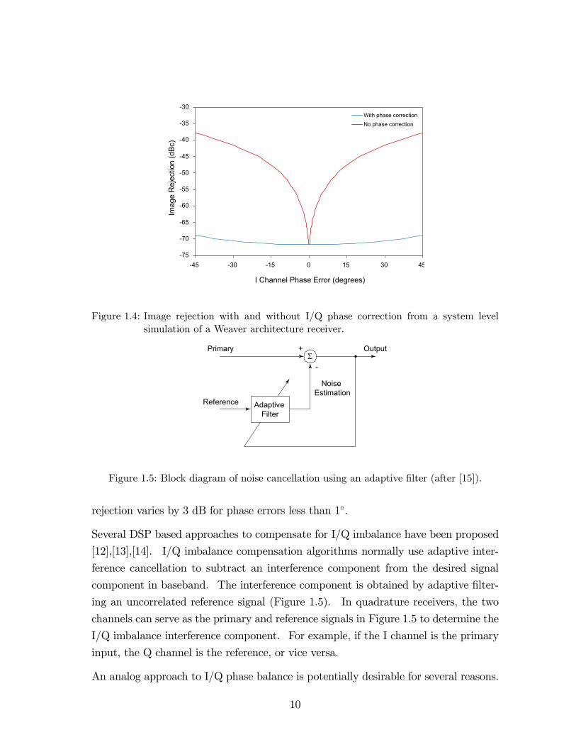
-75
-70
-65
-60
-55
-50
-45
-40
-35
-30
-45 -30 -15 0 15 30 45
I Channel Phase Error (degrees)
Imag
e R
ejec
tion
(dBc
)
With phase correctionNo phase correction
Figure 1.4: Image rejection with and without I/Q phase correction from a system levelsimulation of a Weaver architecture receiver.
Σ
Adaptive Filter
Primary
Reference
Noise Estimation
Output+
-
Figure 1.5: Block diagram of noise cancellation using an adaptive filter (after [15]).
rejection varies by 3 dB for phase errors less than 1.
Several DSP based approaches to compensate for I/Q imbalance have been proposed
[12],[13],[14]. I/Q imbalance compensation algorithms normally use adaptive inter-
ference cancellation to subtract an interference component from the desired signal
component in baseband. The interference component is obtained by adaptive filter-
ing an uncorrelated reference signal (Figure 1.5). In quadrature receivers, the two
channels can serve as the primary and reference signals in Figure 1.5 to determine the
I/Q imbalance interference component. For example, if the I channel is the primary
input, the Q channel is the reference, or vice versa.
An analog approach to I/Q phase balance is potentially desirable for several reasons.
10

-GM L C
V+
V-
Req
Figure 1.6: Block diagram of a negative transconductance (−GM) voltage controlled oscil-lator.
The adaptive filters needed to correct gain and phase balance are iterative. Thus, the
multiple iterations required before phase balance is acquired introduce latency into
the system. Analog tuning of the I/Q phase balance would reduce the DSP compu-
tation requirements and could reduce overall power consumption of an integrated RF
receiver. Therefore, a primary goal of this thesis is to design a phase tunable VCO
which can be used to eliminate I/Q phase error in low-IF receivers and DCRs or to
improve the IRR in a Weaver or Hartley image rejection receiver.
1.2 Voltage Controlled Oscillator (VCO) Design
The receiver architectures described in the previous sections rely on high frequency
VCOs to generate various LO signals (both I and Q). A common VCO topology is
the negative transconductance (−GM) oscillator. A basic block diagram of a −GM
oscillator is shown in Figure 1.6. There are two parts of the oscillator: a −GM circuit
and a parallel LC resonant “tank” circuit. An ideal tank circuit has no loss; if energy
is input into the system, it will oscillate forever at a resonant frequency given by:
f0 =1
2π√LC
. (1.15)
By tuning the tank capacitance (e.g. using a varactor) the frequency of oscillation can
be varied. Real tank circuit implementations have loss associated with the inductor
and capacitor (varactor), represented by the parallel equivalent resistance, Req, in
Figure 1.6. The −GM amplifier provides negative resistance to cancel this loss and
11
allow sustained oscillation of the tank circuit. The average value of the negative
resistance of the −GM amplifier is given by [16]:
−RD = −1/GM = V1/I1
where V1 is the peak voltage of the fundamental at the input and I1 is the peak
current of the fundamental at the output of the active elements. The value of this
negative resistance must be less than the equivalent parallel resistance of the tank
circuit to sustain oscillation. The startup safety factor is often used as a thumb rule
to ensure oscillation in the circuit:
α =Req¯−RD
¯ . (1.16)
The safety factor, α, should be at least 2 for integrated oscillators [17]. VCO design,
therefore, consists of designing the tank circuit to tune over the required frequency
span and the −GM amplifier to supply the necessary negative resistance to sustain
oscillation.
This section discusses three constraints that govern the design of the LC tank and
−GM circuits. First, the aforementioned push toward higher levels of on-chip inte-
gration may require that noisy, synchronous digital circuits be fabricated on the same
chip as noise-sensitive analog and RF circuits. Therefore, VCO designs that are much
less sensitive to substrate or supply noise are required. Second, tight restrictions on
adjacent channels within the crowded frequency spectrum have mandated wireless
standards with very low phase noise requirements for the signal generators. Third,
battery life is a major concern for mobile units, so the design must have low current
consumption. The VCO topology used in this work is presented in the context of
these three constraints.
1.2.1 Substrate and Supply Noise Immunity
In synchronous digital circuits, a clock governs the switching of transistor networks
(gates). This leads to a large number of transistors across the entire chip switching
at approximately the same time. Since CMOS transistors draw the most current
when they are in the process of switching, the voltage rails become very noisy during
12

clock transitions as current draw from the CMOS circuits spikes. This poses no
real problem to traditional digital circuits that have a high degree of noise immunity.
However, analog circuits, which depend on the stability of voltage supply rails to
maintain constant bias points, suffer from the introduction of supply noise from on-
chip digital circuits. To alleviate this problem, analog circuits may share the same
ground but typically have a separate, low-noise supply rail [18].
Another problem for analog circuits is presented by electromagnetic interference cou-
pled into the substrate by signal traces as well as other transistors. The rapid and
continuous switching of on-chip logic gates exacerbates the substrate noise problem.
Substrate noise degrades RF signal quality when it is coupled into the analog portion
of the circuit.
Differential designs are widely employed in the analog part of a system to cancel out
noise. Within localized regions of the IC, substrate and supply noise are approx-
imately the same on both the positive and negative outputs of differential circuits.
Therefore, noise is suppressed in the differential output signal. This cancellation is
called common-mode rejection and is a major advantage of differential topologies.
Differential VCOs are more complex than their single-ended counterparts, since they
require twice the number of transistors to produce positive and negative outputs.
The increased number of devices also increases power consumption and noise. Nev-
ertheless, since on-chip mixers (e.g. Gilbert Cells) are typically differential, a differ-
ential output is required of the signal generator. Despite the added complexity and
higher power consumption, differential VCOs are typically employed in RFICs to take
advantage of common-mode noise rejection, and to avoid the need for single-ended-
to-differential circuits to interface with the other components of the RF system.
1.2.2 Phase Noise
The output of an ideal oscillator can be described by the following equation:
v(t) = A cos(ω0t+ φ) (1.17)
where A is the amplitude of oscillation, ω0 is the frequency of oscillation, and φ is
the phase offset. However, the active and passive devices used to implement a real
13

1/f 3
1/f 2
L(∆
ω)
log∆ω∆ω1/f 3 /2Q
2FkT/P
ω0
s
Figure 1.7: Oscillator phase-noise spectrum.
oscillator introduce random noise into both the amplitude and phase of the output.
The introduction of noise changes equation 1.17 to:
v(t) = A(t) cos(ω0t+ φ(t)) (1.18)
Frequency is the time derivative of the total phase, so the output spectrum of the
oscillator will have sidebands because of random variations in the phase. This is
known as phase noise. The amplitude noise can also manifest itself as phase noise
due to the non-linear, amplitude-limiting nature of an oscillator. Thus, both sources
of noise serve to widen the phase-noise spectrum of the oscillator.
Figure 1.7 shows an oscillator phase-noise spectrum as predicted by Leeson [19].
Three distinct regions of the spectrum exist: the 1/f3 sloped region; the 1/f2 sloped
region; and the noise floor region. The boundary separating the noise floor from
the 1/f2 region occurs at approximately ω0/2Q. The tank circuit filters, or shapes,
the integrated noise spectrum below this frequency. At this frequency, however, the
1/f2 sloped region intersects the phase noise floor of the circuit, which is constant
versus frequency. The boundary at ∆ω1/f3 is related to the 1/f corner frequency of
the active device(s) of the oscillator, which occurs where the 1/f noise intersects the
high frequency shot or channel noise of the device.
Phase noise is measured as a power spectral density in units of decibels below the car-
14

rier per Hertz (dBc/Hz) reported at some offset frequency from the carrier frequency.
For example, the IEEE 802.11a standard requires signal generators to have a phase
noise less than −107 dBc/Hz at a 1 MHz offset from the carrier [20].
The origin of phase noise has been described by Leeson using assumptions of a linear,
time-invariant system. Leeson’s well-known equation for phase noise is [19]:
L (∆ω) = 10 log
(2FkT
Ps·"1 +
µω0
2Q∆ω
¶2#·³1 +
ω1/f3
∆ω
´)(1.19)
where F is the device excess noise factor, k is Boltzmann’s constant, T is the tem-
perature, Ps is the average power dissipated in the resonator, and ω1/f3 is related to
the 1/f noise corner frequency. F and ω1/f3 are not typically known in advance, so
they are usually fitted to measured data. Therefore, this model typically does not
predict measured phase noise results very well.
Since oscillators are fundamentally non-linear circuits, the assumption of linearity
must be examined carefully. The amplitude is limited and controlled in the oscillator
by a combination of the non-linear devices and supply voltage. However, the noise in
equation 1.18 is relatively small compared to the output signal swing. These small
perturbations in the signal swing can be assumed to be linear with respect to the noise-
to-phase transfer function, even though the large signal output amplitude control is
non-linear [21]. Therefore, the principle of superposition is a valid assumption for
the relationship between noise and phase.
The assumption of time-invariance in standard phase noise models must also be exam-
ined. It has been shown that amplitude noise is converted to phase noise differently
if it is injected at a time when the output is near zero as opposed to a time when the
output is at a maximum [22]. Figure 1.8(a) shows how the injection of an amplitude
perturbation, ∆Vn, to the output of a lossless LC tank at the maximum has a smaller
effect on the zero-crossing phase than the same perturbation when the waveform is
near zero [Figure 1.8(b)]. Therefore, time-invariance is a poor assumption for the
noise-to-phase transfer function.
To account for the time-invariance of the noise-to-phase conversion, an impulse sensi-
tivity function (ISF) can be obtained for the output waveform of the oscillator. The
ISF, typically obtained via simulation, weights the effect amplitude noise has on the
15
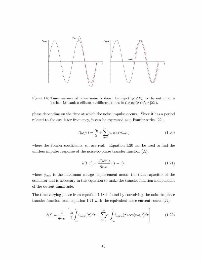
t
Vout Vout
t
Vn∆
Vn∆
Figure 1.8: Time variance of phase noise is shown by injecting ∆Vn to the output of alossless LC tank oscillator at different times in the cycle (after [22]).
phase depending on the time at which the noise impulse occurs. Since it has a period
related to the oscillator frequency, it can be expressed as a Fourier series [22]:
Γ(ω0τ) =c02+
∞Xn=1
cn cos(nω0τ) (1.20)
where the Fourier coefficients, cn, are real. Equation 1.20 can be used to find the
unitless impulse response of the noise-to-phase transfer function [22]:
h(t, τ) =Γ(ω0τ)
qmaxu(t− τ). (1.21)
where qmax is the maximum charge displacement across the tank capacitor of the
oscillator and is necessary in this equation to make the transfer function independent
of the output amplitude.
The time varying phase from equation 1.18 is found by convolving the noise-to-phase
transfer function from equation 1.21 with the equivalent noise current source [22]:
φ(t) =1
qmax
c02
tZ−∞
inoise(τ)dτ +∞Xn=1
cn
tZ−∞
inoise(τ) cos(nω0t)dτ
(1.22)
16

A Fourier series can be used to represent the equivalent noise current:
inoise(t) = I0 +∞X
m=1
Im cos[(mω0 +∆ω)t] (1.23)
where ∆ω is an offset frequency added to allow calculation of phase noise at offsets
from the carrier in the final results. The Fourier coefficients, I0 through Im, are
related to the noise current spectral density in a 1 Hz bandwidth, i2n/∆f .
If equation 1.23 is then substituted into equation 1.22, the only term from the infinite
sum that contributes to the excess phase is the case where n = m. In a sense, this
result corresponds to frequency conversion that occurs in a heterodyne receiver [21].
Essentially, the cn coefficients of the noise-to-phase transfer function act as an LO
signal to down-convert noise at the nth harmonic to two sidebands at ±∆ω from the
oscillation frequency. This down-converted noise has a constant power spectral den-
sity versus offset frequency. However, the down-converted noise has a 1/f2 slope in
the phase-noise spectrum because of the bandpass frequency characteristic of the tank
circuit, which ideally attenuates the noise power contribution from each harmonic at
20 dB per decade increase of ∆ω.
Furthermore, 1/f noise from the active devices is up-converted by the c0 coefficient
from equation 1.22. The 1/f3 region of Figure 1.7 is created by up-converted 1/f
noise at offsets from the carrier below the ∆ω1/f3 corner frequency combined with
the 1/f2 sloped noise from down-converted noise around the harmonics.
Using the representation for φ(t) in equation 1.22, the phase noise power spectral
density in the 1/f3 region of Figure 1.7 can be more accurately predicted by [21]:
L (∆ω) = 10 log
i2n∆f
c20
8q2max∆ω2ω1/f3
∆ω
(1.24)
Phase noise in the 1/f2 region is predicted by [21]:
L (∆ω) = 10 log
i2n∆f
Γ2rms
2q2max∆ω2
(1.25)
where Γrms is the rms value of the ISF given in equation 1.20.
17

The implications of equations 1.24 and 1.25 for oscillator design are significant. First,
the tank circuit Req is responsible for a significant part of the noise current spectral
density, i2n/∆f . Since Req is typically limited by low-Q inductors in integrated VCOs,
increasing theQ of the tank inductor is essential to the design of a low-noise oscillator.
This has traditionally been a problem for Si ICs, because standard Si processes use a
low-resistivity substrate. Aspects of inductor design for higher Q will be discussed
in detail in Chapter 2. Second, the presence of qmax in the denominator of both
equations 1.24 and 1.25 implies that the signal amplitude of the oscillator should
be maximized to obtain lower phase noise. This stems from the assumption that
voltage amplitude noise is assumed to be small compared to the output. Large
oscillation amplitudes minimize the percent change noise has on the output waveform.
Third, equation 1.24 shows that choosing devices with a low 1/f corner frequency
can reduce the close-in phase noise of the 1/f3 region of Figure 1.7. Finally, the
ISF can be optimized to improve phase-noise performance by using differential and
complementary VCO designs [23],[24]. Ideally, the transistors should supply short
pulses of current to restore energy to the tank circuit at the time when the ISF is the
smallest. This will be explored in greater detail in Chapter 3.
1.2.3 Power Consumption
The two obvious ways to reduce VCO power consumption are: (1) reduce the supply
voltage, and (2) reduce the current consumption. This section discusses aspects of
both low-voltage and low-current design for VCOs.
Supply voltage is one of the foremost IC design considerations. Batteries are available
with discrete voltages, so the lowest supply voltage for the given technology which
permits suitable circuit performance is typically selected for the design. The supply
rail must have a high enough voltage such that all the transistors in the design can
operate with stable bias conditions. For bipolar designs, each transistor needs a
sufficient base-emitter voltage (VBE) to turn the device on and a sufficient collector-
emitter voltage (VCE) to keep the device out of saturation. This limits the number
of transistors that can be “stacked” between the rail and ground. This limitation
is referred to as “headroom.” The current source transistors typically suffer most
from limited headroom, since they are usually the closest to ground in a transistor
18

3Q 2Q1Q
refI
VCC
out1I out2I
Figure 1.9: Schematic of a current mirror with two outputs.
stack. They are not required to provide gain (or negative transconductance) so
designers will pull as much VCE as possible from these devices to maximize available
VCE for other devices. However, if the collector voltage drops too much for the
bias transistors, the base-collector junction will become forward biased, pushing the
devices into saturation. If the transistors operate in the saturation regime, the
current they provide can vary drastically for very small changes in collector voltage.
This can have severe consequences on circuit performance.
Power consumption is reduced further by designing for minimal current. Several
design techniques can be used to minimize current in the bias transistors of an oscil-
lator. The number of current references can be reduced by daisy chaining multiple
output devices to one reference (Figure 1.9). This minimizes the number of current
paths from power to ground. In addition, the ratio of the device sizes in the current
mirror should be scaled to minimize the amount of current not directly used to DC
bias the −GM circuit.
Another major factor in lowering current consumption is the design of output buffers
for the oscillator. The oscillator should have a large output signal swing to minimize
phase noise and provide sufficient switching drive to subsequent mixers. However,
this large signal output may compress traditional buffers. Buffers that can handle
large signal input drives usually consume much more current than the oscillator itself,
which substantially increases overall power consumption.
19

VCC
V+ V-
Vctrl
Vbias Vbias
1Q 2Q
tailI
sCsC
2C1C
1L
Figure 1.10: Schematic of the cross-coupled, differential pair oscillator.
1.2.4 Cross-coupled, —GM Oscillator
A common topology for RFIC voltage controlled oscillators is the cross-coupled, dif-
ferential LC oscillator (Figure 1.10). As mentioned previously, in addition to superior
common mode noise immunity over single-ended topologies, the differential output
can be used to drive the LO port of the widely used double-balanced Gilbert cell
mixer. This VCO topology will be the basis for the work in this thesis.
Bipolar transistors (Q1 and Q2) offer three advantages over field-effect transistors
(FETs) in oscillators. First, the typically lower 1/f noise and corner frequency of
bipolar devices results in superior phase noise in the 1/f3 region compared to equiv-
alent FET devices. The origin of 1/f noise is generally attributed to carrier surface
trapping due to defects in the semiconductor material [25],[26]. FET structures typ-
ically have higher 1/f noise, since trapping occurs more readily during lateral carrier
transport along rough surface interfaces in the channel [27]. In contrast, the prob-
ability of carrier trapping in integrated bipolar devices is reduced because transport
occurs vertically through the surface interfaces [28]. Second, shot and thermal noise
of bipolar transistors are lower than the channel noise of FETs. This reduces the
broadband noise at harmonics of the output frequency which are frequency trans-
lated to phase noise in the 1/f2 region. Third, bipolar transistors have a higher
transconductance per milliampere (gm/mA) than FETs, although submicron FETs
20

are closing the gap [29]. Higher gm/mA allows the VCO of Figure 1.10 to consume
less power than a FET based design with the same oscillation amplitude and tank
circuit parallel equivalent resistance.
If Q1 and Q2 are directly coupled, saturation will result in a low oscillation amplitude.
For example, when the collector voltage of Q1 reaches its maximum, if the voltage
difference between the V+ node and the V− node exceeds the forward-bias voltage
of the collector-base junction of Q2, then Q2 will saturate. This problem is avoided
by AC cross-coupling the differential pair with capacitors (CS), thereby providing an
independent bias for the bases (Figure 1.10). The additional cross-coupling capacitors
lower the oscillation frequency, so the tank varactors must be resized to compensate.
For AC-coupled differential pair oscillators, only Itail, the supply voltage, and the
tank circuit Q are variables in the nonlinear control of the oscillation amplitude.
1.3 Silicon-Germanium (SiGe) Technology
Two simultaneous trends in the present semiconductor market suggest that SiGe
BiCMOS may be the technology of choice for low-cost, high-performance RFICs.
The first is the ongoing drive towards greater integration. In this technology, high
performance SiGe transistors are directly available with submicron metal-oxide silicon
field-effect transistors (MOSFETs), allowing for RF and digital circuits to be designed
and fabricated on the same chip. Thus, SiGe processes are often employed to integrate
high performance RF circuits with state-of-the-art high speed digital signal processing
and control.
The second trend is the continued improvement in SiGe device performance, given,
primarily, by two figures-of-merit. First, the small-signal, unity-current-gain fre-
quency (fT ) is an indicator for the maximum frequency at which the transistor can
be used as an amplifier and is given by:
fT =1
2π
·1
gm(Ceb + Ccb) + τ b + τ e + τ bc
¸−1(1.26)
where Ceb (or Cπ) is the emitter-base junction parasitic capacitance, Ccb (or Cµ) is
the collector-base parasitic capacitance, τ b is the base transit time, τ e is the emitter
21

delay time, and τ bc is the base-collector junction depletion layer transit time. A
second figure-of-merit, the maximum oscillation frequency (fMAX), is given by:
fMAX =
sµfT
8πrBCcb
¶(1.27)
where rB is the parasitic base resistance. Often, fMAX is a more useful indicator of the
device RF performance, since it includes the parasitic rB. State-of-the-art SiGe HBTs
have fT and fMAX values on the order of those for equivalent III-V technologies, such
as gallium arsenide (GaAs) and indium phosphide (InP) (i.e., greater than 250 GHz)
[30],[31],[32]. This indicates that SiGe HBT devices can be used for applications
approaching the millimeter wave region (30-50 GHz). It should be stressed that fTand fMAX serve as figures-of-merit; a combination of many factors determines the
actual device performance in practical applications.
The drive for companies to economize, coupled with lower cost and comparable perfor-
mance to III-V devices, has recently enabled SiGe to make inroads in semiconductor
markets previously dominated by III-V technologies. SiGe ICs have become com-
petitive with and even out-perform III-V circuits in some ways. For, example, SiGe
was recently used to produce the lowest reported minimum stage delay of an emitter
coupled logic (ECL) ring oscillator, surpassing the previous standard set using InP
[33].
The two major disadvantages of SiGe technologies have been lossy passives and low
break-down voltages. First, loss in passives comes as a result of the standard low-
resistivity Si substrate which allows submicron CMOS to coexist with SiGe transis-
tors. The semi-insulating substrate of III-V technologies has traditionally allowed
much higher Q factors for monolithic inductors. However, thicker metals and higher-
resistivity substrates in some SiGe processes have recently permitted Q factors on
the order of those achievable in III-V processes. Second, low break-down voltages of
SiGe transistors limits their use as power amplifiers (PAs), an essential component
of any transmitter. However, research and development is currently underway to
improve the high-power capabilities of SiGe devices [34].
22

EC
e-
h+V
∆ g
n emitter
n collector
p base
g
g
Fermi Level
I p
I n
E
E
gE
E
E
e energy
-
h energy
+
e-
IC
IB
I s
I r
h+
Figure 1.11: Bandgap diagram of a traditional wide-bandgap emitter npn HBT (after [36]).
1.3.1 Wide-Bandgap Emitter HBTs
The definition of a heterojunction is a p-n junction where the bandgaps of the n-
material and p-material differ. Si, located in column IV of the periodic table, is an
elemental semiconductor. The traditional Si bipolar junction transistor (BJT) is a
homojunction device, meaning that the base, collector, and emitter all have the same
bandgap (approximately 1.12 eV). The idea of a heterojunction bipolar transistor
(HBT) dates back to one of the original patents by William Shockley for the solid-
state transistor in 1948. Although the advantages of an HBT (to be discussed below)
were long recognized, the technology capable of implementing them was not available
until the 1970s [35],[36]. In addition, until the early 1990s, the only available HBTs
used III-V semiconductor materials.
In a npn homojunction device, the forces acting on electrons and holes are equal and
opposite. Traditional npn heterostructure devices allow the forces on electrons and
holes to be engineered by adjusting the bandgap of the emitter with relation to the
base (∆Eg). Figure 1.11 shows how the potential barrier for hole back-injection into
the emitter from the base in an npn device is larger than the potential barrier for
electron injection into the base. Reduced hole back-injection current (Ip) decreases
the base current (IB) of the wide-bandgap emitter transistor with relation to IC due
to emitter electron-injection current (In). In addition, the emitter recombination
current (Is) is reduced by decreasing Ip, which in turn increases In and IC . Thus,
23
n-AlGaAs
p -AlGaAs+
n-GaAs
n -GaAs+
SiON
Base Contact
Collector Contact
WSi
Emitter Contact
InGaAsn-GaAs
Isolation Region
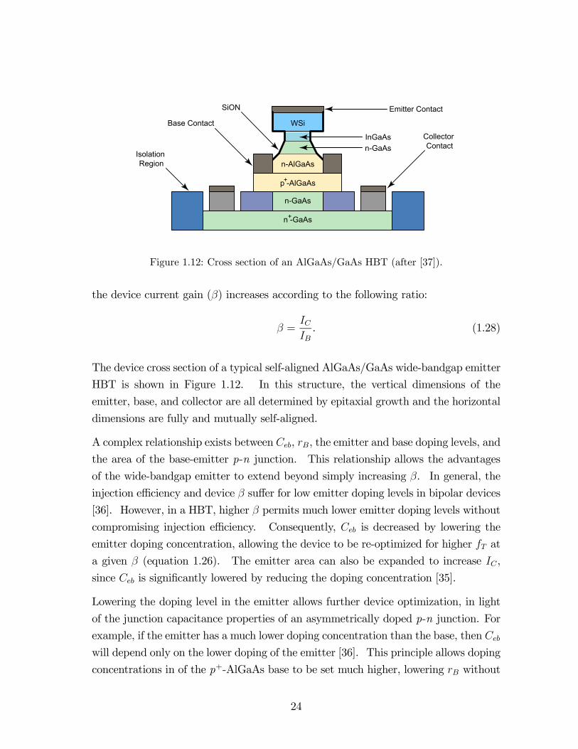
Figure 1.12: Cross section of an AlGaAs/GaAs HBT (after [37]).
the device current gain (β) increases according to the following ratio:
β =ICIB. (1.28)
The device cross section of a typical self-aligned AlGaAs/GaAs wide-bandgap emitter
HBT is shown in Figure 1.12. In this structure, the vertical dimensions of the
emitter, base, and collector are all determined by epitaxial growth and the horizontal
dimensions are fully and mutually self-aligned.
A complex relationship exists between Ceb, rB, the emitter and base doping levels, and
the area of the base-emitter p-n junction. This relationship allows the advantages
of the wide-bandgap emitter to extend beyond simply increasing β. In general, the
injection efficiency and device β suffer for low emitter doping levels in bipolar devices
[36]. However, in a HBT, higher β permits much lower emitter doping levels without
compromising injection efficiency. Consequently, Ceb is decreased by lowering the
emitter doping concentration, allowing the device to be re-optimized for higher fT at
a given β (equation 1.26). The emitter area can also be expanded to increase IC,
since Ceb is significantly lowered by reducing the doping concentration [35].
Lowering the doping level in the emitter allows further device optimization, in light
of the junction capacitance properties of an asymmetrically doped p-n junction. For
example, if the emitter has a much lower doping concentration than the base, then Ceb
will depend only on the lower doping of the emitter [36]. This principle allows doping
concentrations in of the p+-AlGaAs base to be set much higher, lowering rB without
24

affecting Ceb. Low rB is desirable because it improves the gain, noise performance,
and fMAX of the device (equation 1.27).
Widening the bandgap of the emitter, therefore, can be utilized to dramatically im-
prove the high frequency performance of the device. Superior performance has lead
to wide-spread use of these devices in some applications. For example, the III-V HBT
has become the dominant device for PAs in mobile wireless applications due to high
breakdown voltages and power densities (W/mm2), in addition to the aforementioned
improvements in fT and fMAX values.
1.3.2 SiGe HBTs
Si and Ge are both column IV semiconductors. However, Ge has a substantially
lower bandgap of approximately 0.66 eV [38]. Thus, the introduction of Ge into Si
to create a Si1−xGex alloy results in a material with a smaller bandgap than pure
Si. The bandgap of the alloy is dependent on the fractional concentration of Ge
(given by x ≤ 1), with the bandgap being smallest when the concentration of Ge isthe greatest. Therefore, SiGe HBTs have bases that are engineered to have narrower
bandgaps than the emitters.
For example, an npn SiGe HBT is created with an n+-poly-Si/p-SiGe emitter-base
junction and a p-SiGe/n-Si base-collector junction with an implanted n-Si collector
region (Figure 1.13) [39]. SiGe HBTs can certainly be fabricated using a mesa-type
structure as shown in Figure 1.12. However, these structures are not compatible
with thermal processing cycles needed in CMOS technologies, so such HBTs cannot
be integrated in BiCMOS processes. On the other hand, the structure in Figure 1.12
is compatible with the CMOS processing steps; thus, this SiGe HBT structure can
be fabricated alongside submicron FETs [40].
The concentration of Ge in the base is typically graded (Figure 1.14), with the highest
concentration at the base-collector junction to lower the bandgap closer to the collec-
tor. Figure 1.14 shows that the bandgap is essentially unchanged at the emitter, so
the emitter-base junction is approximately the same as that of a conventional homo-
junction Si BJT. Unlike wide-bandgap emitter HBTs, IB of an npn SiGe HBT is not
changed by the heterostructure, since hole back-injection from the base is determined
25

Emitter Contact
Base Contact Collector Contact
poly-Si n +p+ p+
np-SiGe
n +
n +
p -
Shallow Trench
Deep T
rench
Oxide
Metal
Figure 1.13: Cross section of an implanted-collector SiGe HBT (after [41]).
n+ Si emitter
n- Si collector
p-SiGe base
e-
h+
Ge
p-Si
drift field
I p
I n
EC
VE
gE
gEgE
gE
e energy
-
h energy
+
Figure 1.14: Bandgap diagram of Si and SiGe HBT. The red line represents the changedconduction band caused by adding Ge to the base. Below the bandgap diagramis the corresponding Ge concentration profile (after [42]).
26

by the unchanged relative valence bands of the emitter and base. Therefore, the im-
provement in β of SiGe HBTs does not come from reduced IB. On the other hand,
grading the bandgap of the base lowers the potential barrier for electron injection
into the base from the emitter, thereby improving the collector efficiency for a given
emitter-base forward bias. The increase in collector current for a fixed bias translates
to an increase in the current gain (β) and Early voltage (VA) of the device [42].
The Ge gradient also creates a drift field which accelerates electrons in the base trav-
eling from the emitter to the collector, lowering τ b. Furthermore, τ e is reduced, since
it is inversely proportional to β [42]. Lowering both τ e and τ b increases fT accord-
ing to equation 1.26. Furthermore, as in III-V HBTs, rB is lowered by increasing
the doping level of the base relative to the emitter to improve the gain and noise
performance of the device.
An important measure of noise performance is the minimum noise figure (NFmin),
which is determined by broadband noise sources in the transistor. Broadband noise
in bipolar transistors is primarily attributed to base and collector shot noise and
thermal noise. These noise sources are reduced by a combination of decreasing rB
and increasing fT and β [39]. Since all three of these quantities are optimized by the
HBT structure, current SiGe devices can have NFmin as low as 0.4 dB [43]. State-
of-the-art SiGe HBTs have NFmin approximately 1 to 2 dB lower than the best III-V
HBTs, III-V FETs, and CMOS devices [44]. In addition to low broadband noise,
it has been shown that the low frequency 1/f noise of SiGe HBTs is comparable to
the best Si BJT devices and exceeds that of MOSFETs, GaAs HBTs, GaAs high
electron-mobility transistors (HEMTs), and GaAs metal semiconductor field-effect
transistors (MESFETs) by several orders of magnitude [39],[45],[46]. For example,
at 10 Hz, the mean square 1/f noise of SiGe HBTs has been shown to be 10−18 A2/Hz
compared to 10−16 A2/Hz for Si n-FET devices [39]. Superior 1/f noise and NFmin
make SiGe HBTs excellent devices for low-phase noise RF oscillator designs.
1.4 Objective and Overview of Thesis
The objective of this research is to demonstrate the concept of a quadrature LO
source with analog tunable I/Q balance which could potentially be used to improve
27

the performance of I/Q channel receivers and the image rejection of the Weaver
architecture. Analog tunability of quadrature output phase has not been previously
explored in the literature. Three areas determine the feasibility of tunable output
phase, namely: phase flatness, phase tuning range, and overall power consumption.
This thesis analyzes a 5-6 GHz SiGe VCO with tunable I/Q balance in terms of these
three areas.
As part of this work, two VCOs were designed. The first VCO uses an electrically
symmetric inductor, which has a Q factor approximately 50% higher than the tra-
ditional dual inductor structure used in the tank circuit of the second VCO. Aside
from the tank inductors, the two VCOs are identical. Therefore, this thesis also in-
vestigates the improvement in phase noise performance obtained by using the higher
Q electrically symmetric tank inductor. The VCO with the symmetric inductor was
combined with a tunable polyphase filter to create a quadrature LO source with tun-
able I/Q balance. Circuits were designed and fabricated using the Motorola 0.4 µm
CDR1 SiGe BiCMOS process. This process has four aluminum metal layers and a
thick uppermost (bump) copper layer for high performance RF passives.
This chapter has introduced background information regarding the motivation, ap-
plication, and design of a quadrature VCO with tunable phase outputs. A brief
overview of the advantages of SiGe BiCMOS, the technology used for this work, has
also been presented. Chapter 2 discusses the design and characterization of mono-
lithic inductors, specifically for application in differential VCOs. Design procedures
for optimizing Q factor, as well as simulation and characterization of differential in-
ductors are the focus of the material presented. Design and simulation of the −GM
LC VCO using SiGe HBTs is presented in Chapter 3. Chapter 4 covers the design
and simulation of a tunable polyphase network. Measured results for the fabricated
VCO and polyphase are presented in Chapter 5. Chapter 5 also includes information
on fabrication and packaging to facilitate accurate RF test and measurement. This
thesis concludes with an evaluation of circuit performance, as well as a discussion on
future work and possible improvements to the VCO design with tunable quadrature
phase outputs.
28

Chapter 2
Monolithic Inductor Design
Monolithic inductors perform critical roles in integrated RF systems as components
in matching, biasing, and resonant filtering networks. While the drive towards higher
levels of integration has brought about significant performance improvements in recent
years, on-chip inductors (particularly in Si technologies) still lag behind the more
expensive, off-chip, surface mount alternatives. On-chip inductors in Si technologies
can have Quality (Q) factors that range from 3 to 20 compared to several 100s for
off-chip inductors. Acceptable performance can be obtained from on-chip inductors
if the major loss and parasitic capacitance contributions are considered.
This chapter reviews the basic loss mechanisms and the equations used to charac-
terize Q factor and effective inductance value for planar spiral inductors on lossy
Si substrates. Design considerations for differentially excited monolithic inductors
which can help improve Q factor are also discussed. Finally, full-wave electromag-
netic simulations used to characterize and optimize the inductors for this work are
presented.
2.1 Quality (Q) Factor
The Q factor is defined by the following ratio:
Q = 2πfaverage energy stored
energy dissipated per second. (2.1)
29
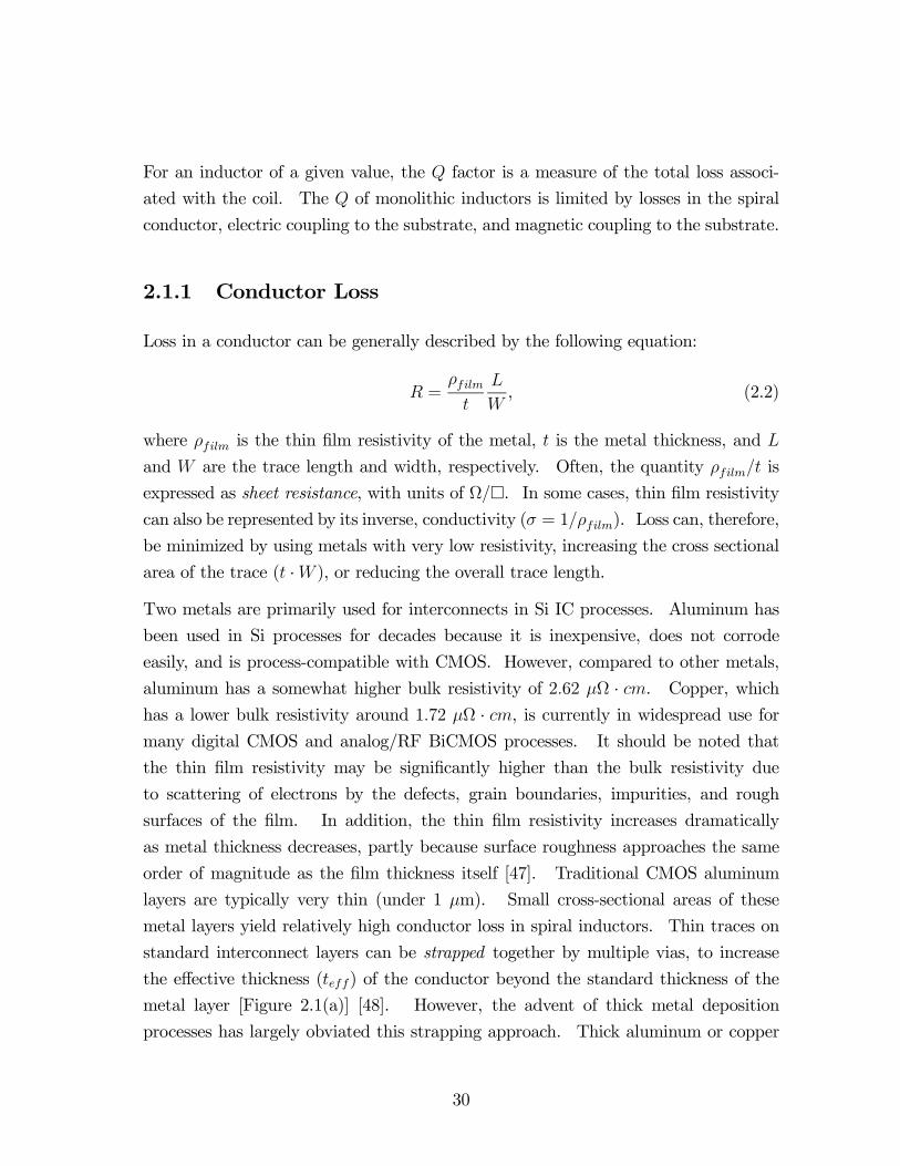
For an inductor of a given value, the Q factor is a measure of the total loss associ-
ated with the coil. The Q of monolithic inductors is limited by losses in the spiral
conductor, electric coupling to the substrate, and magnetic coupling to the substrate.
2.1.1 Conductor Loss
Loss in a conductor can be generally described by the following equation:
R =ρfilmt
L
W, (2.2)
where ρfilm is the thin film resistivity of the metal, t is the metal thickness, and L
and W are the trace length and width, respectively. Often, the quantity ρfilm/t is
expressed as sheet resistance, with units of Ω/¤. In some cases, thin film resistivity
can also be represented by its inverse, conductivity (σ = 1/ρfilm). Loss can, therefore,
be minimized by using metals with very low resistivity, increasing the cross sectional
area of the trace (t ·W ), or reducing the overall trace length.Two metals are primarily used for interconnects in Si IC processes. Aluminum has
been used in Si processes for decades because it is inexpensive, does not corrode
easily, and is process-compatible with CMOS. However, compared to other metals,
aluminum has a somewhat higher bulk resistivity of 2.62 µΩ · cm. Copper, which
has a lower bulk resistivity around 1.72 µΩ · cm, is currently in widespread use formany digital CMOS and analog/RF BiCMOS processes. It should be noted that
the thin film resistivity may be significantly higher than the bulk resistivity due
to scattering of electrons by the defects, grain boundaries, impurities, and rough
surfaces of the film. In addition, the thin film resistivity increases dramatically
as metal thickness decreases, partly because surface roughness approaches the same
order of magnitude as the film thickness itself [47]. Traditional CMOS aluminum
layers are typically very thin (under 1 µm). Small cross-sectional areas of these
metal layers yield relatively high conductor loss in spiral inductors. Thin traces on
standard interconnect layers can be strapped together by multiple vias, to increase
the effective thickness (teff) of the conductor beyond the standard thickness of the
metal layer [Figure 2.1(a)] [48]. However, the advent of thick metal deposition
processes has largely obviated this strapping approach. Thick aluminum or copper
30

teff
t
(a) (b)
Si Substrate Si Substrate
Intermetal dielectric
Figure 2.1: Cross section of two approaches for analog/RF interconnects: (a) mutltiplemetal layers strapped together by vias and (b) thick bump layer metal.
technologies are available for analog designs to reduce conductor loss in passives
[49],[50]. Some processes employ copper for all interconnect layers, while others
have a thick copper layer as the uppermost metal and aluminum (or other metal) for
underlying interconnects. A thick uppermost copper layer is sometimes referred to
as a “bump” layer, since it actually protrudes from the otherwise flat final passivation
layer of the completed IC. These bump layers can be much thicker than standard
interconnect metal layers because the restrictions due to planarization by chemical
mechanical polishing (CMP) are loosened [Figure 2.1(b)]. Increased thickness leads
to much lower series resistance in the spiral and higher Q for two reasons: (1) the
cross sectional area of the conductor is increased and (2) the thin film resistivity is
improved (reduced). The process used for this work (Motorola CDR1) has a ∼10µm thick copper bump layer for high Q inductors [50].
The second way to minimize conductor loss is to modify the planar spiral geometry.
Ideally, very wide traces should be used to maximize the amount of conductor for
a given thickness of the metal layer. A structure with the maximum amount of
conductor in the shortest possible length is desired. The circular spiral is ideal in
this regard; however, the octagonal spiral is more commonly used because of its layout
simplicity. Octagonal spiral layouts only require 45 bends of the conductor, rather
than the smooth, continuous curve of a circle. Despite their increased area for a
given inductance over circular and octagonal spirals, square spirals have been typically
31

Ieddy
BeddyBcoil
Icoil
Icoil
Icoil
Figure 2.2: Eddy currents (Ieddy) generated by the magnetic field of the coil (Bcoil). The ⊗and ¯ symbols represent currents flowing into and out of the page, respectively.(after [52]).
used because they only require 90 bends of the conductor traces. This structure
is mandated by mask generation systems that require Manhattan style layouts (i.e.,
only 90 bends used, like the streets of Manhattan, NY) [51]. The process used
for this work does allow circular structures that fall on a 50 nm grid. However, the
process also has automated layout generation and modeling (parameterized cells) of a
range of octagonal spiral inductors. For these reasons, the octagonal spiral inductor
was used for this work.
Conductor loss also arises when the magnetic field of the inductor penetrates the turns
of the spiral to induce swirling eddy currents according to Faraday’s law (Figure 2.2)
[52]. These eddy currents have a small component in the same direction as current
flow in the inductor. However, the majority of the eddy current flow is in directions
other than that of the inductor coil currents. As a result, the coil current is crowded
to the side of the conductor with the same directional component, minimizing the
effective trace width that the coil current occupies and increasing the loss. As
frequency increases, this current crowding effect becomes more pronounced.
The inner-most turns of the inductor suffer the most from swirling currents, since
the magnetic field is greatest at the center of the coil. It has been shown, using
finite-element simulations of a nine turn inductor, that resistance at 2 GHz in the
outer coil increased 18% from its low frequency value. In contrast, the resistance
32

of the innermost coil increased 480% over the same range [52]. Consequently, the
innermost coils are typically eliminated to leave a large “hollow” area at the center
of the inductor. Since the inner turns contribute minimally to the total inductance,
hollow coils have much higher Q factors without a significant increase in the outer
diameter of the coil.
2.1.2 Shunt Parasitic Capacitance
As shown in Figure 2.1, the metal spiral of the inductor is isolated from the semi-
conductor substrate (typically at ground potential) by one or more dielectric layers
used to separate interconnect layers (inter-metal dielectrics). This creates a parasitic
shunt capacitor that can be roughly approximated by the following equation:
C =A
d(2.3)
where A is the total area of the metal traces, is the dielectric permittivity, and d is
the thickness of the dielectric.
The parallel parasitic capacitance plays a major role in determining the self-resonant
frequency (fsr) of the inductor (i.e., the frequency at which the inductor has a zero
net reactance). Beyond fsr, the planar spiral becomes capacitive. The parasitic
capacitance limits the maximum size of monolithic inductors to a few nanohenries
(nH), since large inductance values require more area (A). Furthermore, the parasitic
capacitance contributes to the loss of the inductor by AC coupling RF energy from
the coils into the substrate (as will be discussed in the next sub-section). The Q
factor versus frequency curve slopes downward to zero at the fsr, so controlling the
parasitic capacitance is also essential to designing the inductor for high Q.
Reducing the conductor width, and thereby reducing the inductor area, minimizes
this parasitic capacitor. However, as discussed previously, conductor loss is in-
creased when narrow traces are used. The designer must balance both the parasitic
shunt capacitance and conductor loss when selecting a conductor width. This trade-
off underscores the advantage of circular and octagonal spirals over square spirals.
For example, for a given operating frequency above fsr, the conductor width can be
increased, thereby decreasing fsr, as long as the peak Q factor is not affected. There-
33

fore, the reduction in overall trace area of circular and octagonal spirals allows wider
traces to be used in order to reduce conductor loss.
The parasitic capacitance can also be reduced by increasing the dielectric thickness,
d, in equation 2.3 and printing the inductor on the uppermost possible metal layer.
If several metal layers are strapped together by multiple vias, careful consideration
should be given to the thickness of the remaining dielectric between the lowest metal
layer of the inductor and the substrate. For, example, binding all the metal layers
together for an ultra-thick conductor may reduce conductor loss, but it will also
substantially increase the shunt parasitic capacitance coupling to the substrate. In
this case there is a trade-off between conductor loss and parasitic capacitance for the
inductor design. This trade-off does not occur for inductors using thick bump metal
layers a fixed distance above the substrate.
There is also parasitic capacitance between the vertical faces of the interwinding traces
or between overlapping traces at cross-under points of the inductor. This capacitance
also contributes to decreasing the fsr, though the effects are typically small compared
to the parasitic capacitance with the substrate in Si technologies. The interwinding
capacitance can be minimized by increasing the spacing between the coils of inductor;
however, this reduces the effective inductance of the coil, requiring a larger coil for
a given inductance value. Typically, the smallest spacing available for the process
is chosen to minimize the overall area of the inductor, regardless of the effect on the
interwinding capacitance.
2.1.3 Substrate Loss
Substrate loss is the dominant factor resulting in low inductor Q factors in a standard
Si processes. This section discusses two types of loss in the substrate: electric
(capacitive) loss and magnetic loss.
The primary source of electric loss in the substrate is RF energy coupled through
the shunt capacitance of the inductor into the substrate. Si CMOS substrates are
typically doped to have a lower bulk resistivity in order to reduce the possibility
of latch-up in digital CMOS circuits. The low-resistivity substrate also improves
noise isolation between digital and analog circuits, since hot-electron induced noise
34

B(t)
-Icoil Icoil
-I substrateI substrate
Image Currents
Figure 2.3: Image currents in the substrate induced by the time varying magnetic field ofthe coil. The ⊗ and ¯ symbols represent currents flowing into and out of thepage, respectively (after [52]).
currents in the substrate are diminished [52]. Unfortunately, the low-resistivity
substrate also appears as a resistor between the parasitic capacitance and ground.
In the past, GaAs has been used almost exclusively for RF/microwave ICs since it
has a semi-insulating (high-resistivity) substrate. For GaAs, the parasitic resistor
representing substrate loss is very large, so the parasitic shunt capacitance appears to
be terminated by an open circuit to RF signals. Since Si is typically a low-resistivity
substrate, the substrate resistor connecting the parasitic capacitance to ground is
relatively small, allowing more of the signal to be coupled into the substrate. High
resistivity substrates and wells, or micromachining techniques can be used to reduce
substrate loss in Si technologies; however, these techniques are non-standard for IC
process flows.
The other type of loss in the substrate is magnetic loss. The magnetic field from the
inductor encircles the current carrying wires, as described by Ampere’s law. Lenz’s
representation of Faraday’s law states that an opposing image current is induced
in any conductor within the magnetic field to resist a change in the field. As the
time-varying, RF current flows in the inductor, image currents are induced in the Si
substrate in the opposite direction (Figure 2.3). The Si substrate acts much like a
transformer to couple energy from the inductor into the substrate. More than 60%
of the loss in the inductor can be attributed to this parasitic transformer [53]. As
with the parasitic shunt capacitance, the effect of the parasitic transformer can be
35

minimized by decreasing the diameter of the coil [52]. For smaller coils, the mag-
netic flux lines into the substrate are less dense, thereby inducing less image current.
Conceptually, moving the spiral farther from the substrate would tend to reduce the
effect of the parasitic transformer, since the magnetic field decreases in strength at
greater distances from the coil. However, the relatively small changes in distance
between standard interconnect metal layers, is not large enough to make a significant
difference in the strength of the magnetic field penetrating the substrate [52]. In con-
trast, high-resistivity substrates prevent image currents from being induced, which
greatly benefits the Q factor.
As mentioned previously, the magnetic flux lines are most dense in the center of the
inductor spiral. Therefore, it is critical to keep the area under the center of the
coil free from any interconnect traces or active devices. Anything located inside the
spiral will tend to couple energy away from the inductor and increase the loss beyond
that due to the image currents in the substrate. The return path of the magnetic
flux lines are located on the outside of the spiral. Though these flux lines are much
less dense than those inside the coil, it is still a good idea to locate interconnects
and active devices a fair distance away from the coil. For the technology used for
this work, it is recommended that a distance of 100 µm be used between the outside
diameter of the coil and the nearest metal trace or active device.
2.2 Inductor Model and Characterization
Inductor characterization depends on the specific application. Three different uses
for inductors in RF circuits are shown in Figure 2.4. The first [2.4(a)] is a shunt
connection typically used for degeneration, impedance matching, or loading. This
configuration is characterized as single-ended, or unbalanced, since one port of the
inductor is connected to AC ground (this is sometimes accomplished by way of a
shorting capacitor at DC bias nodes). The second [2.4(b)] is a series connection,
which is useful for impedance matching in amplifiers or mixers. The third [2.4(c)] is a
differential excitation, commonly used in differential oscillators, differential amplifiers,
and mixers. For example, the VCO in Figure 1.10 requires this inductor topology
for the resonant tank circuit. This configuration requires precise symmetry between
the two sides of the inductor to set up a virtual ground at the plane of symmetry.
36

IL
V1V1 V+ V-
Virtual Ground
(a) (b) (c)
ωL V1 - ω ILL
ωL
ωL/2 ωL/2
Figure 2.4: Three possible uses for inductors in RF circuits (a) shunt (b) series, and (c)differential.
A lumped element model is useful for accurate simulation of monolithic inductors.
Figure 2.5 shows a detailed model for an inductor on Si substrates that takes into
account the effects described in Section 2.1 [53]. The inductance of the coil is modeled
by the series inductor (L) between ports 1 and 2. The parasitic capacitive coupling
into the substrate and the associated losses are represented by the shunt capacitors
(COX and Csub) and resistors (Rsub). Trace conductor loss is characterized by a
resistor (Rs) in series with the inductor. The loss due to image currents magnetically
induced into the substrate is represented by the transformer coupled to a resistor
(Rsub(m)). The cross under and interwinding capacitance is represented by Cp.
The model of Figure 2.5 can be represented by a π-equivalent Y -parameter network
(Figure 2.6). The impedance of differentially excited inductors, such as the structure
in Figure 2.4(c), is measured between ports 1 and 2 of Figure 2.6, rather than with a
simple one-port measurement of the input impedance with port 2 grounded. For this
reason, inductance and Q factor are calculated differently for differential inductors
than for traditional single-ended configurations [51]. Appendix A gives a detailed
development of how this network is simplified for both the single-ended and differential
cases in order to determine the Q factor and inductance.
As shown in Appendix A, neither port of the differential inductor is grounded, so the
impedance seen between the two terminals of the inductor is defined as:
Zin = R+ jX =Y11 + Y22 + 2Y12Y11Y22 − Y 2
12
. (2.4)
37

L RCox
Cp
Rsub(m)
Rsub Csub
Port 1 Port 2
RsubCsub
Coxs
1:n
Figure 2.5: A lumped element model for monolithic inductors on Si substrates (after [53]).
Using equation 2.4, the differential inductance is then defined as:
L =X
2πf=
µ1
2πf
¶·Im
µY11 + Y22 + 2Y12Y11Y22 − Y 2
12
¶¸, (2.5)
and the differential Q factor is defined as:
Q =X
R=
hIm³Y11+Y22+2Y12Y11Y22−Y 212
´ihRe³Y11+Y22+2Y12Y11Y22−Y 212
´i . (2.6)
Measuring an inductor differentially typically results in Q factors slightly higher than
the single-ended case (3-5%) [51].
2.3 Electrically Symmetric Differential Inductors
One method to construct a monolithic differential inductor is to use two inductors,
each of half the total inductance value, placed side by side and connected at the
common node by an underpass on a lower metal layer [Figure 2.7(a)]. In this thesis,
38

-Y12
Y +Y 1211 Y +Y 1222
Port 1 Port 2
Figure 2.6: A π-eqivalent Y -parameter network of the lumped element model for monolithicinductors on Si substrates (see Figure 2.5) [51].
(a) (b)
B (t)1
B (t)2
i1 i2
v1 v2
i1 i2
i1
B (t)2B (t)1
i2
v1 v2
Figure 2.7: Magnetic fields created by the current running through the differentially excitedinductor for (a) dual inductor (b) symmetric inductor. The ⊗ and ¯ symbolsrepresent magnetic fields flowing into and out of the page, respectively.
this layout is referred to as a “dual inductor.” While the coils are geometrically
symmetric, they are not electrically symmetric. The two inductors individually
operate in a single-ended fashion, much like those represented in Figure 2.4(a) and (b),
until they meet at the common node. The main disadvantage of the dual inductor
layout for differential excitation is that the currents (i1 and i2) in the two coils of
the dual inductor flow in the opposite directions where the two coils are adjacent.
As a result, the induced magnetic fields [−→B 1(t) and
−→B 2(t)] are oriented in opposite
directions. These opposing magnetic fields lower the mutual inductance of the dual
inductor, thereby reducing the net reactance without affecting the resistance. Since
Q factor is the ratio of the reactance and resistance, the Q is effectively lowered by
39

these opposing magnetic fields. This effect can be minimized by increasing the gap
separating the two coils. However, this results in an increase in die size for a small
increase in Q – rarely a viable solution.
The magnetic fields of the dual inductor structure could be oriented in the same
direction by reflecting one of the coils in Figure 2.7(a) about its vertical axis. In this
case currents would flow in the same direction where the coils are adjacent, enhancing
mutual coupling. However, this configuration is not desirable because the inductor
is no longer geometrically symmetric. This asymmetry obscures the location of the
virtual ground point. Furthermore, this solution offers no significant reduction in die
area over the dual inductor in Figure 2.7(a).
Figure 2.7(b) shows an inductor with both geometric and electrical symmetry [54].
In this thesis, this layout is referred to as a “symmetric inductor.” Current in adja-
cent coils flow in the same direction so that the induced magnetic fields are oriented
in the same direction. Furthermore, the two halves of the inductor are arranged so
that currents from the positive and negative inputs flow in neighboring coils, a truly
odd-mode structure. Interwinding the differential inductor provides a better match
between the two halves of the coil, resulting in equivalent substrate parasitics. Fi-
nally, Figure 2.7 emphasizes the dramatic decrease in the chip area (& 50%) requiredfor symmetric inductors of the same value.
Past research has shown the improvement inQ factor for symmetric inductors [55],[56].
Theoretically, two times the Q factor is possible with the symmetric inductor, al-
though Qs from 30% to 50% higher than a dual inductor equivalent are realized in
practice [54]. The symmetric inductor requires twice the number of vias and un-
derpasses to intertwine the two coils and make the common node available to the
exterior of the coil (e.g., for biasing). Loss associated with these vias mitigates some
of the Q improvement. Strapping two layers of metal together with multiple vias can
minimize loss in the underpasses that connect opposite halves of the coil. However,
strapping the two layers together is not necessary for the common node underpass
that will be at AC ground, since this trace carries minimal RF signal. Regardless,
the benefit of orienting the two magnetic fields in the same direction far outweighs
these additional sources of loss, as shown by the net improvement in Q factor.
40

2.4 Inductor Simulations
2.4.1 Selection of Inductor Dimensions
Sonnet em [57], a full wave electromagnetic solver, was used to simulate the tank
circuit inductors for the VCO designs in this thesis (Figure 1.10). Three meshing
schemes for the inductor metal are available from Sonnet. The first is the traditional
square mesh. This mesh often requires many cells to accurately represent objects
with angles other than 0 or 90. A second option is the diagonal mesh, which allows
arbitrary angles to be more accurately represented using approximately the same
number of cells as the square mesh. Both of these traditional meshes can require
large amounts of memory to solve Maxwell’s equations for complex structures such
as the differential inductor. The third method, “conformal” meshing, is currently
in beta testing [58]. This mesh was designed specifically to reduce the number
of cells required to accurately simulate meandering lines such as the coils of spiral
inductors. The accompanying reduction in memory requirement dramatically reduces
computation time, making iterative design more feasible. Unfortunately, the beta
version of conformal mesh available when the VCOs were being designed was found
to be less accurate than the diagonal and rectangular mesh for Q calculations. Thus,
long computation times were required (e.g. days versus hours), and, consequently,
exhaustive iterative design was not done to select the final inductor dimensions.
The technology design kit for this work contains automated layout parameterized cells
(p-cells) for octagonal symmetric inductors with three input parameters: trace width;
coil spacing; and inner diameter. The dimensions selected for the inductor represent
design decisions based on the trade-offs discussed in Section 2.1. The minimum
coil spacing for the inductor (7 µm) was selected. Small coil spacings increase the
mutual inductance of the coils and decrease the outer diameter, though at the expense
of increased inter-winding capacitance (Section 2.3). Thus, Q factor is increased for
small coil spacings by reducing the effective area of the inductor for a given inductor
value, though fsr may be lowered as a result. A trace width of 15 µm was selected
over the maximum trace width for the copper bump layer for the process (20 µm).
The decision was made based on the assumption that, at the maximum trace width,
the substrate losses for the larger inductor area would begin to outweigh the benefits
41

710
15
20
7
10
13
1512
13
14
15
16
17
18
19
20
Trace width (um)
Coil spacing (um)
Q fa
ctor
Figure 2.8: Plot of Q factor for various trace widths and coil spacings from electromagneticsimulations of a symmetric inductor with a value of approximately 2.3 nH.
of reducing conductor losses with wide traces.
Several months after the final designs were submitted for fabrication, Sonnet released
an updated and improved algorithm for the conformal mesh. The disagreement
with the standard diagonal and rectangular meshes was reduced, enabling the use of
conformal mesh for accurate, iterative inductor simulation. With the updated version
of Sonnet em, several specific cases with various the trace widths, coil spacings and
inner diameters were simulated to evaluate the design decisions made for the final
inductor. The trace width was varied from 20 µm down to 7 µm. Coil spacing
was swept from 7 µm up to 15 µm. The inner diameter parameter was adjusted to
maintain a total effective inductance value of ∼2.3 nH for different trace widths andcoil spacings.
Figure 2.8 shows the change in Q that results from increasing trace width and coil
spacing. The highest Q is obtained for the maximum trace width (20 µm) and the
smallest coil spacing (7 µm). Contrary to previous assumptions, the Q at the largest
trace width does not suffer from the increased substrate effects. The Q at a trace
42

width of 15 µm is approximately 5% lower than that of an inductor with 20 µm trace
width. Though the selected inductor dimensions provide a Q very near the maximum
available, the inductor design could clearly have benefitted from simulations of an
exhaustive sweep of inductor dimensions. It should be noted, however, that at a coil
spacing of 7 µm, the 15 µm trace width reduces the area of the inductor by 20% over
the 20 µm trace width, which did help with fitting all the required circuits in the
available reticle, since several copies of the inductor were required.
2.4.2 Inductor Design Simulations
Several process parameters play a critical role in accurate inductor simulation. Spe-
cific information on the substrate and inter-metal dielectric layers cannot be presented
in this thesis as it is Motorola proprietary information. However, their general ef-
fect on the inductor simulations should be discussed. Thickness, relative dielectric
permittivity ( r), and loss tangent (tan δ) are essential parameters for the layers sepa-
rating the metal traces and the the substrate. These dielectric parameters determine
the parasitic shunt capacitance described in Section 2.1.2. The thickness and con-
ductivity of the substrate is critical for accurate simulation of image currents and
other substrate losses. The thin film conductivity of the metals for each layer is also
necessary to account for conductor loss. Each of these parameters was obtained from
the CDR1 design manual and included in Sonnet layer definition files.
Two inductor designs were simulated and compared using Sonnet. The first was a
symmetric inductor to be used in the VCO tank circuit. An equivalent dual inductor
was also simulated for comparison in an otherwise identical VCO circuit (Figure 1.10).
Both of the inductors were laid out in Cadence Virtuoso [59] and exported to Sonnet.
Symmetric Inductor Simulations
Both conformal and diagonal meshing schemes were used to simulate the symmetric
inductor. The S -parameters from the simulations were used in conjunction with
equations 2.5 and 2.6 to calculate the resulting differential effective inductance and
Q factor. Figure 2.9 compares the results for both types of meshing. Though the
results are not identical, both meshing schemes yield approximately the same curves
43

-15
-10
-5
0
5
10
15
20
0 5 10 15 20 25
Frequency (GHz)
I n d u
c ta n
c e (n
H)
0
2
4
6
8
10
12
14
16
18
20
Q u a
l i ty
F a c t
o r (Q
)
L (conformal)
L (diagonal)
Q(conformal)
Q(diagonal)
Figure 2.9: Inductance and Q factor results from Sonnet simulations for the symmetricinductor.
for Q factor and effective inductance. Thus, the major benefit of a conformal mesh
simulation is that it requires only 1/10th the simulation time to obtain nearly the
same results as the traditional diagonal mesh simulations. This dramatic decrease
in simulation time makes it practical to perform parameter sweeps to arrive at an
optimal inductor geometry, as presented in Figure 2.8. Based on the conformal mesh
simulations at 5.25 GHz, Sonnet predicts a Q of 18.4 and an effective inductance
value of 2.4 nH.
Dual Inductor Simulations
An equivalent dual inductor was also simulated in Sonnet using both meshing schemes.
Figure 2.10 shows the differential inductance andQ factor from bothmeshing schemes.
The results from conformal and diagonal mesh simulations are nearly identical for the
dual inductor. Based on the conformal mesh simulations at 5.25 GHz, Sonnet predicts
a Q of 11.8 and an effective inductance value of 3.1 nH.
A difference in the relative number of conformal mesh cells used between the sym-
metric and dual inductor cases may explain the improved correlation of simulated
data for the dual inductor. Each of the turns of the dual octagonal inductor was
44

-10
-8
-6
-4
-2
0
2
4
6
8
10
12
0 5 10 15 20 25
Frequency (GHz)
I ndu
c tanc
e (n
H)
0
2
4
6
8
10
12
14
Qu a
l i ty
Fa ct
o r (Q
)
L (conformal)
L (diagonal)
Q (conformal)
Q (diagonal)
Figure 2.10: Inductance and Q factor results from Sonnet simulations of the dual inductor.
broken into eight metal subsections. Only the sections that were at 45 angles used
conformal meshing, since the major time saving advantage of conformal mesh is with
shapes that do not lie on a Manhattan grid. For the conformal mesh simulations,
much of the inductor is still simulated using the diagonal mesh. In the symmetric
inductor case, the coils are treated as one continuous piece of metal, so most of the
inductor is simulated using the conformal mesh. Simulation time was decreased for
the conformal mesh simulations of the dual inductor by ∼75%, though the ratio ofconformal to diagonal mesh cells was less.
Q Factor Comparison
Figure 2.11 compares the simulated Q factors of the symmetric and dual inductors.
At 5.25 GHz, the symmetric inductor has a Q of 18.4 and the dual inductor has
a Q of 11.8. The symmetric inductor layout improves the simulated Q factor by
64% over the dual inductor case, which is comparable to other reported results [54].
Interestingly, the dual inductor has a higher fsr than the symmetric inductor. This
implies that the symmetric inductor has slightly higher parasitic capacitance than
the dual inductor, most likely due to increased cross-under capacitance.
45

0
2
4
6
8
10
12
14
16
18
20
0 5 10 15 20 25
Frequency (GHz)
Q u a
l i ty
F a c t
o r (Q
)
Symmetric Dual
Figure 2.11: Simulated Q factor for the symmetric and dual inductors
2.5 Summary
This chapter has presented information on the loss mechanisms of monolithic induc-
tors on Si substrates. The symmetric inductor, with an approximately 50% improve-
ment in Q factor and more than 50% reduction in die area over the equivalent dual
inductor, was discussed. Iterative simulations of various symmetric inductor dimen-
sions were used to find optimal dimensions to maximize Q, given the area constraints
of the final circuit. Results from full-wave, electromagnetic simulations showed that
a symmetric inductor has an effective inductance of 2.4 nH and a Q of 18.4 at 5.25
GHz. Similar simulations of an equivalent dual inductor resulted in an effective in-
ductance of 3.1 nH and a Q of 11.8 at 5.25 GHz. VCO designs based on both of
these inductor structures are discussed in the next chapter.
46

Chapter 3
VCO Design
As discussed in Chapter 1, VCO design can be separated into two sections: the pas-
sive tank circuit and the active −GM circuit. This chapter first discusses several
important trade-offs which influence design decisions for these circuits. The remain-
ing sections of this chapter cover the simulated performance of the VCOs designed in
this work, output buffer design, and the layout of the VCOs and output buffers.
3.1 Tank Circuit Design
Factors in the design of the tank circuit inductor to maximize Q factor were discussed
in Chapter 2. This section focuses on the trade-offs between the relative size of the
tank inductor and the varactors. A varactor is a tunable capacitor realized using
either a p-n junction diode or a MOS gate capacitor. A brief discussion of the
varactors used in this work is also included.
3.1.1 Inductor Value and Tuning Range
Large inductors are desired for their higher equivalent parallel resistance, Req, as
shown by the following relationship [17]:
Req = Q2πf0L. (3.1)
47

1/N
LPFΣf ref f out
Kd KvKLPF
VCOPhase/ Frequency
Detector
Frequency Divider
+
-
Figure 3.1: Block diagram of a phase locked loop.
As discussed in Chapter 1, the absolute value of the negative resistance, |−1/GM |, ofan oscillator must be less than the Req of the tank circuit in order to sustain oscilla-
tion. Therefore, a larger Req requires less negative resistance from the −GM circuit
for oscillations to occur, thereby reducing the current consumption of the oscillator.
Furthermore, the excess negative resistance (above that which is needed to overcome
loss in the circuit) increases the output amplitude. Continually increasing negative
resistance, however, does not mean continuously increasing output amplitude. The
supply voltage and nonlinear amplitude control of the oscillator ultimately control the
maximum amplitude. Nevertheless, when Req is decreased, the oscillator can have a
higher output amplitude for a given negative resistance.
Meanwhile, large inductors also have lower fsr and require a correspondingly smaller
tank capacitance for oscillation at a given f0 (see equation 1.15). Therefore, the size
of the inductor is usually determined by the size of the tank capacitors and varactors
which provide the precise amount of tuning for the frequency band of the design.
The tuning range and varactor size often determine the usability of the oscillator. For
instance, a VCO is typically used as a component within a phase-locked loop (PLL)
(Figure 3.1). A PLL takes an input reference frequency and generates a control
voltage that forces the output of the VCO to track the reference phase or frequency.
The reference is typically produced by a very frequency stable crystal oscillator at a
much lower frequency. A frequency divider can be used to translate the output of
the VCO to the same frequency range as the reference. Phase locking corrects the
problem of frequency drift inherent in free running oscillators [17].
48

In PLL design, the VCO gain,Kv, is a useful quantity describing the tuning sensitivity
and is given by the following equation:
Kv =∆f0∆Vctrl
(3.2)
where ∆Vctrl is the change in control voltage required to produce a corresponding
change in output frequency, ∆f0. Depending on the application, PLLs are often
required to tune across a wide bandwidth. A VCO for IEEE 802.11a is required to
tune from 5.15 to 5.825 GHz. If the varactor tunes the VCO over this band for a 2
V change in bias, Kv is 338 MHz/V. Unfortunately, it is very difficult to design a
PLL using a VCO with such a high Kv because very small changes in control voltage
(possibly due to noise) can produce drastic changes in output frequency.
Typically, a VCO used in an application requiring a large tuning range over several
bands will employ digitally switched capacitors for coarse band tuning and a varactor
for fine tuning across a given band [43]. This technique lowers the effective Kv,
allowing the VCO to operate stably within a PLL.
In this work, the VCO is intended to drive a tunable polyphase filter on-chip. For
simplicity, the VCO tank circuit was designed with two series connected varactors
(see Figure 1.10) that provide tuning across all three of the U-NII bands from 5.15 to
5.825 GHz, rather than employing the added complexity of switched fixed capacitors
and varactors that tune across the three U-NII bands individually. Though this
large Kv is not desirable for PLL applications, the proof-of-concept of tunable phase
outputs is the primary purpose of this work.
3.1.2 Varactors
The varactors used in this work are accumulation-mode devices. These devices
are similar to PMOS transistors except that the source and drain regions are n+
diffusions in an n-well and the gate is a n+ polysilicon gate (Figure 3.2). The two
n+ regions are tied together to create one node of the varactor, while the gate serves
as the other node. The highest capacitance is obtained when the device operates in
the accumulation regime (i.e., a positive gate bias with respect to the bulk attracts
excess electrons to the interface of the substrate and gate oxide), whereas the lowest
49

n+ n+
n-well
p- epi p- epi
p- epi
V
V
1
2
"S" "D""G"
Figure 3.2: Cross section of an accumulation Mode varactor (after [17]).
capacitance is obtained when the device operates in the depletion regime (i.e., a
negative gate bias with respect to the bulk pushes the electrons deeper into the
substrate, depleting the channel).
MOS varactors typically have very steep “DC” C -V tuning characteristics [60]. How-
ever, if a MOS varactor is used in a differential VCO, the large signal output across
the device modulates the capacitance in the time domain, “smoothing” the DC small
signal tuning characteristic [61]. For this reason, the VCO tuning characteristic is
typically more gradual than the DC C -V tuning characteristic of the varactors. The
Motorola CDR1 varactor DC/small-signal tuning curve is shown in Figure 3.3. The
capacitance tuning range is 115% for bulk-to-gate voltages (Vbg) from −0.8 to 1.7V. Using equation 1.15, the expected frequency tuning range of the VCO is 49% if
the varactor alone is considered. In practice, the tuning range will be lower due to
parasitic and fixed capacitance in the VCO.
3.2 —GM Circuit Design
The primary goal for designing the −GM circuit is to cancel the Req of the tank
circuit, while providing low noise and high oscillation amplitude with acceptable cur-
rent consumption. Section 1.2.2 describes how up-converted 1/f noise manifests
itself in the close-in phase-noise spectrum. Therefore, reducing 1/f noise is a con-
50

0
0.2
0.4
0.6
0.8
1
1.2
-0.8 -0.6 -0.4 -0.2 0.0 0.2 0.4 0.6 0.8 1.0 1.2 1.4 1.6
Vbg (V)
Rel
ativ
e C
apac
itanc
e
Figure 3.3: “DC”/small-signal tuning characteristic of the accumulation mode varactor usedin the VCO of this work.
cern while designing the −GM circuit. In addition, the oscillation amplitude and
negative resistance of the circuit are determined by the bias point of the transistors.
Thus, trade-offs involving device size and transistor biasing play a critical role in well
designed −GM circuits for RF oscillators.
3.2.1 Device Size Trade-Off
It has been shown that increasing emitter area of Si/SiGe bipolar transistors lowers
the 1/f noise for the same base current [62],[63]. However, the current required to
bias for peak fT also increases with device size (Figure 3.4). Therefore the device
should be large to minimize 1/f noise, but not so large that the power consumption
suffers in order to bias for peak fT . For this work, the emitter area (Le × We) was
chosen to be relatively large at 0.4 µm × 10 µm.Emitter area also affects the transconductance of the device. The IC for an npn
device at a particular VBE is given by the equation [64]:
IC =qADnnpo
WBeVBE/VT . (3.3)
51
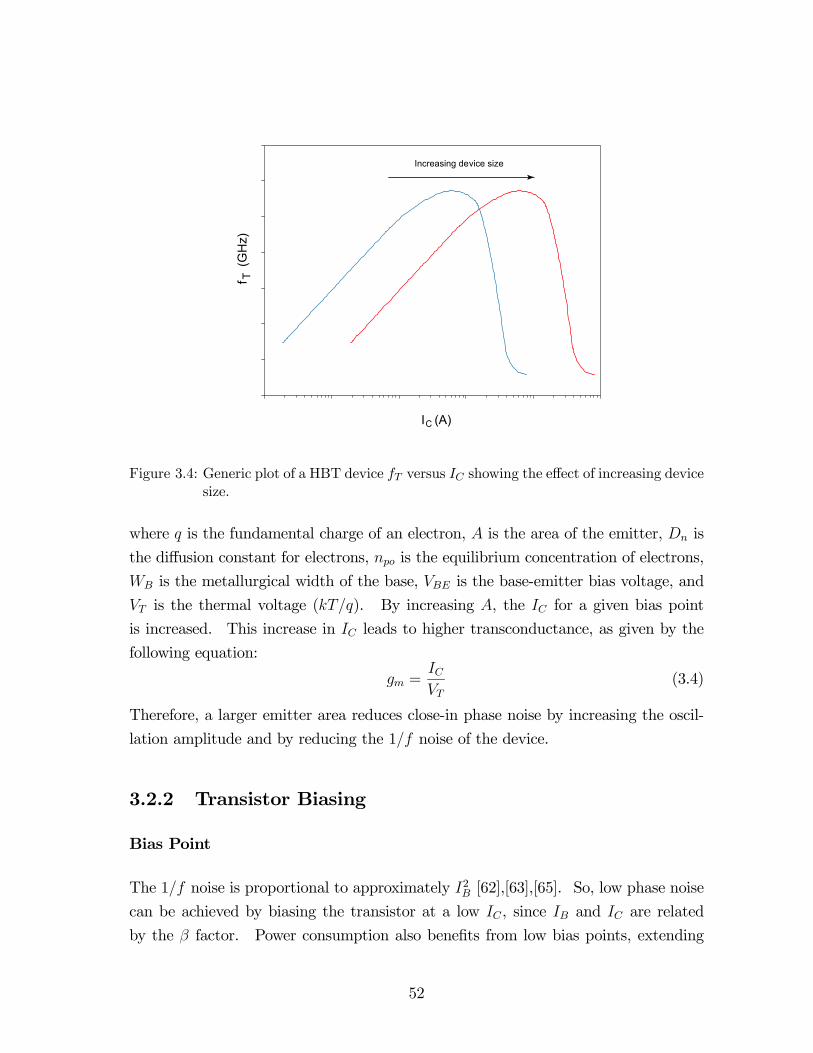
IC (A)
f (
GH
z)T
Increasing device size
Figure 3.4: Generic plot of a HBT device fT versus IC showing the effect of increasing devicesize.
where q is the fundamental charge of an electron, A is the area of the emitter, Dn is
the diffusion constant for electrons, npo is the equilibrium concentration of electrons,
WB is the metallurgical width of the base, VBE is the base-emitter bias voltage, and
VT is the thermal voltage (kT/q). By increasing A, the IC for a given bias point
is increased. This increase in IC leads to higher transconductance, as given by the
following equation:
gm =ICVT
(3.4)
Therefore, a larger emitter area reduces close-in phase noise by increasing the oscil-
lation amplitude and by reducing the 1/f noise of the device.
3.2.2 Transistor Biasing
Bias Point
The 1/f noise is proportional to approximately I2B [62],[63],[65]. So, low phase noise
can be achieved by biasing the transistor at a low IC, since IB and IC are related
by the β factor. Power consumption also benefits from low bias points, extending
52

IC (A)
β
0
20
40
60
80
100
120
140
1.0E-10 1.0E-08 1.0E-06 1.0E-04 1.0E-02 1.0E+00
= 106.3β
I = 1.45 mAc
(a)
1Q
+- VEB
(b)
Figure 3.5: (a) Device β versus IC for a Motorola CDR1 SiGe HBT with emitter dimensionsof 0.4 µm × 10 µm. (b) Test circuit for measuring the Gummel and β curvesof a bipolar device.
battery life for mobile units. Unfortunately, a low IC produces low output oscillation
amplitudes. Section 1.2.2 describes how a high output amplitude is desired for low
phase noise since it is measured as a ratio of the noise to the carrier amplitude (dBc).
Figure 3.5(a) shows β as a function of IC for the devices used in this work. This β
curve is obtained by sweeping the emitter-base voltage of the circuit in Figure 3.5(b)
and measuring the IB and IC Gummel curves. The device β peaks at just over 120
when IC is on the order of several hundred nanoamps. Ideally, the device should
be biased for the peak β to maximize the trade-off between high IC (to increase the
output amplitude) and low IB (to decrease 1/f noise). However, the maximum β for
the Motorola CDR1 HBT occurs for an IC that is far too low to provide sufficient
−GM to offset the loss in the tank circuit. Therefore IC must be selected after the
point where enough transconductance is provided, but before the sharp roll-off of the
β curve. For this work, IC was selected at 1.45 mA (β = 106.3), since this bias point
provides a high oscillation amplitude without a tremendous sacrifice of the peak β of
the device. This bias current occurs just before the β curve of Figure 3.5 begins its
sharper descent.
53

V+ V-
-GM Circuit
Tank Circuit
Current Ref.
Tail Current Source
Base Bias
1Q 2QsCsC
2C1C
1L
3Q 4Q5Q
6Q
2R
1R
BR BR
E3R E4R E5RsC sC
tailI
C1I C2I
Vtail
VVCO
Vctrl
Figure 3.6: Schematic of the VCO and bias circuit.
Bias Circuit
Figure 3.6 shows the complete VCO and bias circuit used in this work. The bias
network consists of a current mirror with two output devices to provide the base bias
voltage and the tail current of the −GM circuit. The bias currents, IC1 and IC2, are
set in both transistors of the cross-coupled differential pair (Q1 and Q2) by the tail
current provided by the output of the current mirror consisting of transistors Q3 and
Q5. These transistors were designed to have a mirror ratio of approximately 16:1 to
minimize the DC current not directly used by the −GM circuit (i.e., consumed by the
reference circuit).
Q6 improves the gain for the mirrored currents in Q3 and Q4 [64]. Figure 3.7(a) shows
a simplified ideal current mirror which uses a diode-connected reference transistor
(Qm1). In this circuit, Qm1 and Qm2 have the same emitter areas, so the collector
current of Qm2 exactly mirrors the collector current of Qm1. The reference (Iref)
must supply base current to Qm1 and Qm2 in addition to the collector current of Qm1,
due to the finite β of the transistors. Thus, the current supplied by Qm2 is lower than
54
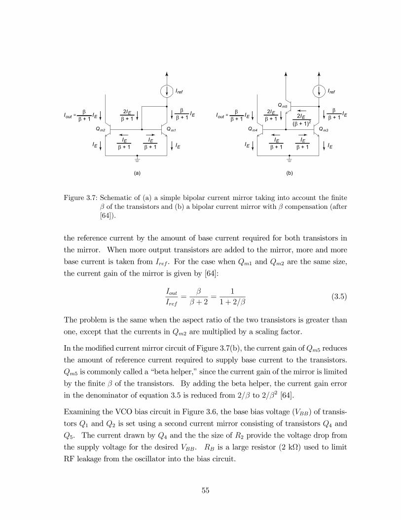
m2Q m1Q
refI
EIEI
EIβ
β + 1EI
ββ + 1β + 1
E2I
β + 1EI
β + 1EI
outI =
m4Q m3Q
refI
EIEI
EIβ
β + 1EI
ββ + 1β + 1
E2I
β + 1EI
β + 1EI
outI =
β + 1)E2I
( 2
(a) (b)
m5Q
Figure 3.7: Schematic of (a) a simple bipolar current mirror taking into account the finiteβ of the transistors and (b) a bipolar current mirror with β compensation (after[64]).
the reference current by the amount of base current required for both transistors in
the mirror. When more output transistors are added to the mirror, more and more
base current is taken from Iref . For the case when Qm1 and Qm2 are the same size,
the current gain of the mirror is given by [64]:
IoutIref
=β
β + 2=
1
1 + 2/β(3.5)
The problem is the same when the aspect ratio of the two transistors is greater than
one, except that the currents in Qm2 are multiplied by a scaling factor.
In the modified current mirror circuit of Figure 3.7(b), the current gain ofQm5 reduces
the amount of reference current required to supply base current to the transistors.
Qm5 is commonly called a “beta helper,” since the current gain of the mirror is limited
by the finite β of the transistors. By adding the beta helper, the current gain error
in the denominator of equation 3.5 is reduced from 2/β to 2/β2 [64].
Examining the VCO bias circuit in Figure 3.6, the base bias voltage (VBB) of transis-
tors Q1 and Q2 is set using a second current mirror consisting of transistors Q4 and
Q5. The current drawn by Q4 and the the size of R2 provide the voltage drop from
the supply voltage for the desired VBB. RB is a large resistor (2 kΩ) used to limit
RF leakage from the oscillator into the bias circuit.
55

The emitter degeneration of Q3, Q4, and Q5 (RE3, RE4, and RE5) aids in increasing
the output impedance of the current mirrors. For example, an approximation for the
output resistance of the degenerated tail current source (Q3) is found using the small
signal output resistance of the device (ro) [66]:
r0o ' ro
µ1 +
IC3RE3
VT
¶. (3.6)
The output resistance of the device is approximated by ro ' VA/IC, where VA is the
Early voltage. For example, using the Early voltage of the Motorola CDR1 HBT
(95 V), a tail current of 2.8 mA and an emitter degeneration resistance of 30 Ω, the
small signal output resistance of the tail source is increased by a factor of 4.2 from
34 kΩ to 140 kΩ.
The increase in output impedance of the mirror provides stability to the output
current. The collector current of a finite output resistance npn bipolar transistor
increases gradually for larger values of VCE. By increasing the output resistance of
the mirror, the collector current remains more constant for increasing VCE. Ideally,
the tail current is supplied to the −GM circuit at a virtual ground point in the VCO
circuit. However, device mismatch can offset the virtual ground, permitting RF
voltage swing from the −GM circuit to affect the collector voltage of Q3. Adding
emitter degeneration reduces the influence of a changing VCE on the DC current
supplied by Q3.
The main benefit of stabilizing the current supplied by Q3 is the potential for lower
phase noise. Any fluctuations in the DC tail current will change the peak output
voltage of the VCO in a similar manner to the voltage noise injected to the output
swing of a lossless LC tank circuit shown in Figure 1.8. As discussed in Section 1.2.2,
amplitude noise is translated to phase noise through the nonlinear amplitude control
of the VCO.
3.3 VCO Simulations
The VCO was simulated using SpectreRF, a component of the Cadence Design Sys-
tem [59]. Typically, the initial simulations of an oscillator are used to verify the
56

proper frequency and amplitude of the output waveform in the time domain. These
simulations are used to fine tune performance based on the trade-offs described in
Sections 3.1 and 3.2. In addition to the time-domain analysis, non-linear simulations
are required to predict oscillator phase noise.
Two VCOs were simulated in this work. Both VCOs are identical except that the first
uses a symmetric differential inductor and the second uses a dual inductor in the tank
circuit (see Chapter 2). The difference in overall VCO performance due to the 50%
difference in Q factor is compared in this section. The S -parameters generated from
full-wave electromagnetic simulation are used in SpectreRF to simulate the VCOs.
These S-parameters allow more accurate simulation of the parasitic capacitance and
resistance than the generalized models of the p-cell inductors included with the design
kit.
3.3.1 Transient Simulation
For the symmetric inductor VCO transient simulations, the tank varactor control
voltage is set to 2.5 V, tuning the oscillator to the low end of the frequency tuning
range. Figures 3.8 and 3.9 show the steady-state voltage and current waveforms at
the collectors of Q1 , Q2 , and Q3 from Figure 3.6 (i.e., the V+ and V− terminals
and the collector of the tail current bias transistor of the VCO). These plots show
that the −GM transistors turn off fairly well during their negative VCE half cycles and
that the current waveforms have little harmonic content when the transistors conduct.
Furthermore, V+ and V− can swing above the rail voltage due to the inductive load
provided by the tank circuit inductor. Figure 3.9 shows the relationship between the
tail current and the collector currents in Q1 and Q2.
Recalling that the zero crossing points of an oscillating, lossless LC tank circuit
are minimally affected by voltage noise injected in the system when the output is
maximum (Figure 1.8), the waveforms in Figures 3.8 and 3.9 suggest that the cross-
coupled, differential pair oscillator will have good phase noise performance. The
transistors inject the majority of their noise into the oscillating tank circuit when
they turn on to conduct current. Figure 3.10 plots the collector current spikes from
Q1 and Q2 along with the differential output voltage swing. The current spikes
occur just after the maxima and minima of the output swing, so very little current
57

0
0.5
1
1.5
2
2.5
3
3.5
0 20 40 60 80 100 120 140 160 180 200
Time (ps)
No d
e V o
l ta g e
(V )
tail
v+v-
Figure 3.8: Voltage waveforms from time domain simulations of the VCO with a symmetricinductor.
-2
0
2
4
6
8
10
0 20 40 60 80 100 120 140 160 180 200
Time (ps)
C o l
l e c t
o r C
u rre
n t (m
A )
Ibias
tail
C2 C1ii
i
Figure 3.9: Current waveforms from time domain simulations of the VCO with a symmetricinductor. The Ibias of a single device is shown, for reference.
58
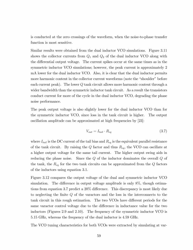
is conducted at the zero crossings of the waveform, when the noise-to-phase transfer
function is most sensitive.
Similar results were obtained from the dual inductor VCO simulations. Figure 3.11
shows the collector currents from Q1 and Q2 of the dual inductor VCO along with
the differential output voltage. The current spikes occur at the same times as in the
symmetric inductor VCO simulations; however, the peak current is approximately 2
mA lower for the dual inductor VCO. Also, it is clear that the dual inductor permits
more harmonic content in the collector current waveforms (note the “shoulder” before
each current peak). The lowerQ tank circuit allows more harmonic content through a
wider bandwidth than the symmetric inductor tank circuit. As a result the transistors
conduct current for more of the cycle in the dual inductor VCO, degrading the phase
noise performance.
The peak output voltage is also slightly lower for the dual inductor VCO than for
the symmetric inductor VCO, since loss in the tank circuit is higher. The output
oscillation amplitude can be approximated at high frequencies by [23]:
Vout = Itail ·Req (3.7)
where Itail is the DC current of the tail bias andReq is the equivalent parallel resistance
of the tank circuit. By raising the Q factor and thus Req, the VCO can oscillate at
a higher output voltage for the same tail current. The higher output swing aids in
reducing the phase noise. Since the Q of the inductor dominates the overall Q of
the tank, the Req for the two tank circuits can be approximated from the Q factors
of the inductors using equation 3.1.
Figure 3.12 compares the output voltage of the dual and symmetric inductor VCO
simulation. The difference in output voltage amplitude is only 8%, though estima-
tions from equation 3.7 predict a 20% difference. This discrepancy is most likely due
to neglecting the finite Q of the varactors and the loss in the interconnects to the
tank circuit in this rough estimation. The two VCOs have different periods for the
same varactor control voltage due to the difference in inductance value for the two
inductors (Figures 2.9 and 2.10). The frequency of the symmetric inductor VCO is
5.15 GHz, whereas the frequency of the dual inductor is 4.59 GHz.
The VCO tuning characteristics for both VCOs were extracted by simulating at var-
59

-1.5
-1
-0.5
0
0.5
1
1.5
0 20 40 60 80 100 120 140 160 180 200
Time (ps)
V o l ta
g e (V
)
-2
0
2
4
6
8
10
C o l
l e c t
o r C
u rre
n t (m
A )
C2 C1
vout(t)ii
Figure 3.10: Plot of the collector current waveforms with the differential output voltageswing from time domain simulations of the VCO with a symmetric inductor.
-1.5
-1
-0.5
0
0.5
1
1.5
0 50 100 150 200
Time (ps)
Vol
tage
(V)
-2
0
2
4
6
8
10
Col
lect
or C
urre
nt (m
A)
C2 C1
vout(t)ii
Figure 3.11: Plot of the collector current waveforms with the differential output voltageswing from time domain simulations of the VCO with a dual inductor.
60
-1.5
-1
-0.5
0
0.5
1
1.5
0 50 100 150 200
Time (ps)
Vol
tage
(V)
Symm VCO
Dual VCO
Figure 3.12: Comparison of the differential output voltage swing of the dual and symmetricinductor VCOs for tank varactor control voltages of 2.5 V.
ious varactor tuning voltages. Figure 3.13 shows that the expected tuning range of
the symmetric inductor VCO is from 4.64 to 6.31 GHz for tuning voltages from 0.7
to 3.2 V. Using the linear tuning range of the VCO from 1.9 to 2.7 V, the Kv of
the symmetric inductor VCO is 1.15 GHz/V. As for the dual inductor VCO, the
slightly larger inductance value in the tank circuit lowers the tuning characteristic
compared to the symmetric inductor VCO. The simulated tuning range of the dual
inductor VCO is from 4.06 to 5.96 GHz for tuning voltages from 0.7 to 3.2 V. In
the linear range of the tuning curve, the Kv is 1.36 GHz/V. The simulated tuning
range of the symmetric inductor VCO (31%) and the dual inductor VCO (38%) are
slightly more than half the expected tuning range of 49% calculated from the varactor
tuning range (see Section 3.1.2). This implies that the combination of parasitic and
fixed capacitance in both VCOs is on the order of the capacitance of the varactor
[17]. The larger tuning range of the dual inductor is most likely due to the higher fsr(i.e., lower parasitic capacitance) as shown previously in Figure 2.11. As discussed
in Section 3.1.2, the slope of the tuning curve shown in Figure 3.13 is more gradual
than the DC C -V characteristic of the varactor in Figure 3.3. The linear region of
the VCO tuning curve extends across 1.0 V, rather than 0.5 V as was the case with
the varactor DC/small-signal tuning curve.
61

4
4.2
4.4
4.6
4.8
5
5.2
5.4
5.6
5.8
6
6.2
6.4
0.7 1.2 1.7 2.2 2.7 3.2Control Voltage (V)
Freq
uenc
y (G
Hz)
Symm VCODual VCO
Figure 3.13: Plot of the tuning characteristic for both the symmetric and dual inductorVCOs.
3.3.2 Non-Linear Simulations
Phase noise characterization requires that the non-linear, frequency translation effects
of the oscillator be accounted for. The non-linear simulator for SpectreRF is Periodic
Steady State (PSS). This non-linear simulator first determines the steady-state so-
lution of the oscillator in the time domain using a shooting method [67]. A shooting
method determines initial conditions which lead directly to steady-state operation of
the circuit. PSS requires an initial estimate for the output frequency of the oscillator,
usually obtained from transient simulations. The simulator then iterates to solve for
the actual operating frequency of the oscillator in addition to the steady state initial
conditions.
Once the time varying steady-state circuit conditions are obtained over an entire
period, non-linear effects such as phase noise can be simulated. Traditional small-
signal analyses in SPICE find small perturbations from the fixed DC operating point
of the circuit. Similarly, PSS performs small signal analyses to the time varying
operating point obtained using the shooting method. Using noise as a small signal
input to the time varying operating point of the oscillator, the phase noise can be
calculated using linear, time varying analysis [68].
62

VOUT IDC Phase Noise at 1 MHz Tuning RangeVCO (V) (mA) Offset (dBc/Hz) (GHz)
Symmetric 1.18 2.5 −118 4.64− 6.31Dual 1.09 2.6 −118 4.06− 5.95
Table 3.1: Various simulated characteristics of the symmetric and dual inductor VCOs. TheDC currents are for a supply voltage of 2.5 V and the frequency tuning rangesare for tank varactor control voltages from 0.7 to 3.2 V.
One significant disadvantage of PSS analysis is that distributed element networks,
such as S-parameter blocks, require infinite dimensional state vectors [68]. Dis-
tributed element networks must be either modeled as a network of lumped elements
or converted to the time domain using a Fast Fourier Transform before simulation.
Thus, S -parameter data from electromagnetic simulation of inductor structures (as in
Chapter 2 Section 2.4) cannot be directly used as an N -port block in PSS simulations.
However, a circuit block is available from Motorola CDR1 support that translates S -
parameter files to a linear model compatible with PSS simulations. The non-linear
simulated data presented in this thesis uses this circuit block in conjunction with the
Sonnet simulated S -parameters of the inductors. The Harmonic Balance Analysis
simulator, available in Agilent Advanced Design System (ADS) [69], is preferred for
nonlinear simulation of distributed networks; however, the Motorola CDR1 design kit
does not support ADS models.
Contrary to expectations, PSS simulations of both the symmetric and dual inductor
VCOs resulted in nearly the same phase-noise spectrum (Figure 3.14). Based on
an expected 50% improvement in Q factor alone, Leeson’s equation predicts that
the improvement in phase noise for the symmetric inductor over the dual inductor is
proportional to 10 log(1/Q2), or 3.5 dBc/Hz. However, the phase noise difference is
likely greater than 3.5 dBc/Hz for these two VCOs because, in addition to a higher Q
inductor, the output power is greater for the symmetric inductor VCO (see equation
1.19). SpectreRF PSS predicts that both VCOs have a phase noise of −118 dBc/Hzat 1 MHz offset and −98 dBc/Hz at 100 kHz offset, exceeding the IEEE 802.11a phasenoise specification of −107 dBc/Hz at a 1 MHz offset from the carrier. The results
of the linear and non-linear VCO simulations are summarized in Table 3.1.
63

-150
-140
-130
-120
-110
-100
-90
-80
100K 1M 10MFrequency (Hz)
Phas
e N
oise
(dBc
/Hz)
Symm VCODual VCO
Figure 3.14: Simulated phase noise of the symmetric and dual inductor VCOs.
3.4 VCO Output Buffer Design
The output of the symmetric inductor VCO is a 1.2 V peak sine wave delivered into a
2 kΩ differential load, or −1.4 dBm. The initial design for the output buffer was anHBT differential pair with no input or output impedance matching. Unfortunately,
large signal inputs from the VCO to the differential pair compress the buffer and clip
the sine waves. Since the VCO is intended for use as the LO pump for a balanced
mixer, the distortion of the waveform is not necessarily a problem; the ideal input for
a mixer is actually a rail-to-rail square wave that switches the mixing core abruptly.
However, the simulations of the differential pair buffer connected directly to the VCO
output show that the peak voltage drops from 2.4 V differential at the output of the
VCO to 1.6 V differential at the output of the buffer. The less than unity voltage gain
of the buffer is a result of operating the amplifier well into the compression region.
A buffer that maintains approximately the same voltage level as the VCO output is
obviously more desirable.
This work uses a pair of class-B, push-pull, CMOS buffers because their compression
points are much higher than that of a simple differential pair. The buffer is designed
and laid out in a manner similar to a digital inverter, except that the gates must be
DC biased so that both the NMOS and PMOS transistors operate in the saturation
64
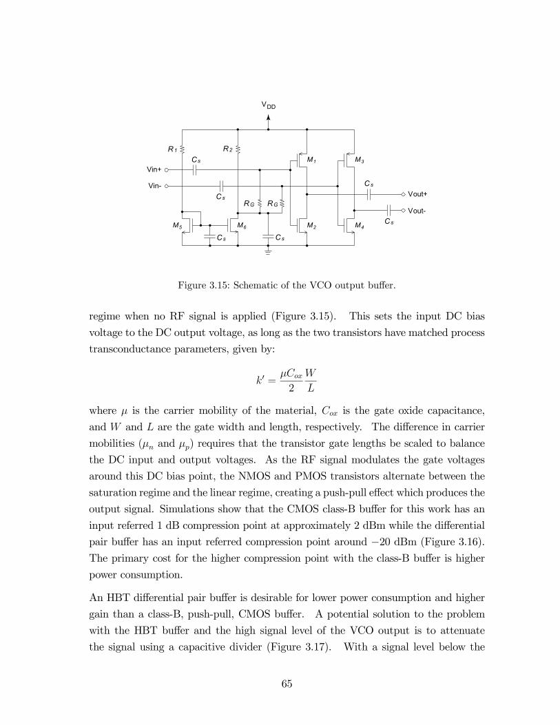
Vin+
Vin-Vout+
Vout-
5M 6M 2M
1M
4M
3M1R 2R
GR GR
sC
sC
sC
sC
sC
sC
VDD
Figure 3.15: Schematic of the VCO output buffer.
regime when no RF signal is applied (Figure 3.15). This sets the input DC bias
voltage to the DC output voltage, as long as the two transistors have matched process
transconductance parameters, given by:
k0 =µCox
2
W
L
where µ is the carrier mobility of the material, Cox is the gate oxide capacitance,
and W and L are the gate width and length, respectively. The difference in carrier
mobilities (µn and µp) requires that the transistor gate lengths be scaled to balance
the DC input and output voltages. As the RF signal modulates the gate voltages
around this DC bias point, the NMOS and PMOS transistors alternate between the
saturation regime and the linear regime, creating a push-pull effect which produces the
output signal. Simulations show that the CMOS class-B buffer for this work has an
input referred 1 dB compression point at approximately 2 dBm while the differential
pair buffer has an input referred compression point around −20 dBm (Figure 3.16).
The primary cost for the higher compression point with the class-B buffer is higher
power consumption.
An HBT differential pair buffer is desirable for lower power consumption and higher
gain than a class-B, push-pull, CMOS buffer. A potential solution to the problem
with the HBT buffer and the high signal level of the VCO output is to attenuate
the signal using a capacitive divider (Figure 3.17). With a signal level below the
65

1 dB compression point
-40
-30
-20
-10
0
10
20
30
-40 -30 -20 -10 0 10
Input Power (dBm)
Out
put P
ower
(dBm
)
HBT Differential PairCMOS Class-B Push-Pull
Figure 3.16: 1 dB compression curves of the HBT differential pair buffer and the class-B,push-pull CMOS buffer.
2C1C
inV outV
Figure 3.17: Capacitive divider that can be used to attentuate the VCO output before thebuffer.
compression point of the buffer, the signal can be fed to an HBT differential pair.
The output node in Figure 3.17 should be biased with a low-noise source, since any
noise at this node could couple back into the oscillator and increase the phase noise.
Though, in a sense, the generation of a high output power signal in the oscillator is
wasted by using the attenuator, a design with a high-gain, HBT differential pair buffer
can potentially consume less power than those with buffers with a higher compression
point. This allows the VCO core to be designed with a high amplitude output swing
for low-phase noise performance and the output buffer to be designed for low-power
consumption. Future revisions of the VCO in this work will utilize such a capacitive
divider topology.
66

Figure 3.18: Layout of the core VCO used in the symmetric and dual inductor VCOs. Diearea occupied is 190 µm × 192 µm.
3.5 VCO Layout
The two VCO designs are identical aside from the different tank inductor imple-
mentations. For proper comparison, both VCOs use the same layout for the −GM
circuit, bias circuit, and tank varactors. Figure 3.18 shows the layout of the VCO
core common to both designs. The layout is symmetric about the x-axis of the figure
to improve the differential performance of the VCO. The only exception to this sym-
metry is the current reference and base bias transistors located at the top of Figure
3.18. The outputs of the VCO are taken from the upper plates of the AC coupling
capacitors of the −GM transistors at the upper and lower right corners of the figure.
The wide diagonal traces on the right side of the figure connect the circuit with either
the symmetric or dual inductor in the final VCO layouts. The area of this portion
of the VCO is 190 µm × 192 µm.Figures 3.19 and 3.20 show the buffered, symmetric inductor and dual inductor VCO
layouts with pads, respectively. The V+ and V− output buffers are placed along either
side of the VCO core. These buffers have input and output DC blocking capacitors.
The input blocking capacitors allow the buffer to be biased for class-B operation while
67

Figure 3.19: Buffered symmetric inductor VCO with pads. The total die area (includingpads) is 1 mm × 0.76 mm.
Figure 3.20: Buffered dual inductor VCO with pads. The total die area (including pads)is 1.2 mm × 0.76 mm.
68
the output blocking capacitors are included to facilitate integration with a tunable
polyphase circuit (to be discussed in the Chapter 4). The only difference between
these two layouts is the tank inductor. All the pad locations except for the VV CO pin
are identical in both layouts. In the dual inductor VCO, the die must be stretched
to accommodate the larger area of the dual inductor, so the VV CO pin is located an
additional 150 µm further from the other pads compared to the symmetric inductor
VCO.
Four separate supply voltage pads exist for both layouts. The Vtail pad is connected
to the supply rail for the current mirror which provides the tail current of the VCO.
Both the Vbuf+ and Vbuf− pads are connected to the supply rails of the positive and
negative output buffers, respectively. The fourth power supply pad, VV CO, provides
power to the −GM cross-coupled differential pair through the tank inductor. On
the right side of the chip, the differential RF output bond pads (RF+ and RF−) and
interconnects from the output buffers are laid out symmetrically to provide the same
phase offset for both outputs. Moreover, the pads are located so that bond wires of
equal lengths can be extended from the pads to the package pins.
At the time this work was performed, the Motorola CDR1 design kit for Cadence
had limited support for parasitic extraction of the layout. Rather than alter the
design based on the results of a somewhat unreliable extraction tool, the design was
submitted based on the simulations presented in Section 3.3. Since these simulations
use the S -parameters from electromagnetic simulation of the inductor, the design
takes into account the parasitic capacitance and resistance of the inductor, but not
those of the interconnect routing in Figures 3.19 and 3.20.
3.6 Summary
This chapter has presented the design, simulation, and layout of two differential
VCOs. The VCOs are identical except that one uses the symmetric differential
inductor and the other uses the dual inductor, which were presented in Chapter 2.
Simulations of the symmetric inductor VCO predict a differential output amplitude
of 1.18 V compared to 1.09 V for the dual inductor VCO. Spectre PSS simulations
also predict that both VCOs will have a phase noise of −118 dBc/Hz at a 1 MHz
69

offset from the carrier for both VCOs (these results are not believed to be accurate).
The symmetric inductor VCO has a simulated tuning range from 4.64 to 6.31 GHz
for tuning voltages from 0.7 to 3.2 V. In comparison, the dual inductor VCO has
a simulated tuning range from 4.06 to 5.95 GHz over the same range of control
voltages. The symmetric VCO design is intended to be coupled with a tunable
polyphase circuit (presented in the next chapter) to realize a quadrature VCO with
phase tunable outputs.
70

Chapter 4
Tunable Polyphase Filter Design
This chapter presents the circuit design and layout of a tunable polyphase filter. As
described in Chapter 1, LO sources with tunable phase outputs can potentially be
used to improve image rejection in Weaver or Hartley architectures, or eliminate I/Q
phase error in direct conversion or low-IF receivers. The tunable polyphase design
presented here is subsequently integrated with the symmetric inductor VCO design
from Chapter 3 to realize a phase-tunable quadrature output VCO.
4.1 Polyphase Filters and RC -CR Networks
Polyphase filters are derived from the classical RC -CR phase-shift network shown in
Figure 4.1(a). This circuit has two voltage transfer functions, one for each output
referenced to the input. The V1,in to V1,out transfer function is:
F11 (ω) =V1,outV1,in
=1
1 + jωRC(4.1)
and the V1,in to V2,out voltage transfer function is:
F21 (ω) =V2,outV1,in
=−jωRC1 + jωRC
. (4.2)
A 90 difference in the two output phases exists for all input frequencies due to the
−j term in the numerator of equation 4.2. There is, however, only one frequency
71
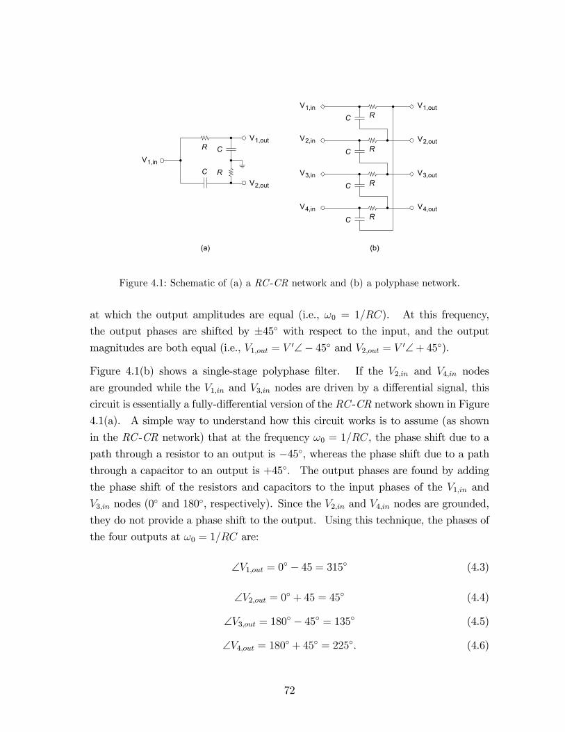
V1,in
V3,in
V2,out
V1,out
V4,out
V3,out
RC
RC
RC
RC
R C
RCV1,in
V2,out
V1,out
(a) (b)
V2,in
V4,in
Figure 4.1: Schematic of (a) a RC -CR network and (b) a polyphase network.
at which the output amplitudes are equal (i.e., ω0 = 1/RC). At this frequency,
the output phases are shifted by ±45 with respect to the input, and the outputmagnitudes are both equal (i.e., V1,out = V 0∠− 45 and V2,out = V 0∠+ 45).
Figure 4.1(b) shows a single-stage polyphase filter. If the V2,in and V4,in nodes
are grounded while the V1,in and V3,in nodes are driven by a differential signal, this
circuit is essentially a fully-differential version of the RC -CR network shown in Figure
4.1(a). A simple way to understand how this circuit works is to assume (as shown
in the RC -CR network) that at the frequency ω0 = 1/RC, the phase shift due to a
path through a resistor to an output is −45, whereas the phase shift due to a paththrough a capacitor to an output is +45. The output phases are found by adding
the phase shift of the resistors and capacitors to the input phases of the V1,in and
V3,in nodes (0 and 180, respectively). Since the V2,in and V4,in nodes are grounded,
they do not provide a phase shift to the output. Using this technique, the phases of
the four outputs at ω0 = 1/RC are:
∠V1,out = 0 − 45 = 315 (4.3)
∠V2,out = 0 + 45 = 45 (4.4)
∠V3,out = 180 − 45 = 135 (4.5)
∠V4,out = 180 + 45 = 225. (4.6)
72

= +
Input Sequence
Positive Sequence
Negative Sequence
V1,in
V3,in
V2,out V2,out
V3,out V3,out
V1,out
V4,out
V1,out
V4,out
Figure 4.2: Illustration of quadrature generation from a single differential input signal (after[70]).
Vin+
Vin-
VI-
VI+
VQ-
VQ+
RC
RC
RC
RCGND
Figure 4.3: Block diagram of a buffered single-stage polyphase filter.
For a more detailed discussion, Appendix B presents the frequency dependant equa-
tions for the output phase, based on the derivation of the voltage transfer function
matrix of the polyphase and RC -CR networks.
From equations 4.3 through 4.6, a single differential input signal is decomposed by
the polyphase into a positive and a negative rotating quadrature sequence (Figure
4.2). The polyphase network rejects the negative rotating sequence and passes the
positive sequence to the output if the input frequency is at the 1/RC pole. Thus,
in addition to quadrature signal generation, the polyphase filter can be used directly
for image rejection [70].
The polyphase network introduces frequency dependant loss, requiring the use of dif-
ferential buffer amplifiers to maintain signal strength (Figure 4.3). The nonlinearity
73
of the buffers can result in amplitude to phase distortion, limiting the exact quadra-
ture phase difference between output nodes to frequencies near ω0 = 1/RC. The
phase flatness versus frequency can be improved by using multiple polyphase stages
and staggering the 1/RC poles; however, adding such stages increases loss, so the gain
requirements and power consumption of the buffers will also increase [71]. If input
and output buffers are used, the gain can be distributed between them to reduce the
requirement from any individual buffer.
The input impedance of the filter also depends on the frequency. Both the shunt
capacitors and the series DC blocking capacitors before the buffers at the output give
the polyphase a highly capacitive input impedance. At the pole frequency, the input
impedance of one input reduces to R k (1/jωC). As a rule of thumb, the poles shouldbe placed such that the lowest impedance is at the input and the highest impedance
is at the output to reduce cascaded loss [70]. Since the polyphase input impedance
can be very low, a buffer serves to de-couple the input of the polyphase from the
driver circuit.
Another design issue for these networks is component mismatch in the four paths,
which can create gain and phase imbalance in the quadrature outputs. While com-
ponents with large areas decrease the impact of mismatch, the parasitic capacitance
and resistance can have a much larger effect on output imbalance. Minimization of
these parasitics requires careful attention to layout symmetry.
4.2 Tunable Phase Outputs
DC bias requirements at the inputs of the output buffers require that series blocking
capacitors be used at the output of the RC -CR network. The transfer function of
these series capacitors with an equivalent load resistance RL is:
G (ω) =jωRLCs
1 + jωRLCs. (4.7)
The phase angle of this transfer function is:
∠G (ω) = 90 − tan−1 (ωRLCs) . (4.8)
74

V1,in
GND
V3,in
V2,out
V1,out
V4,out
V3,out
R
C
R
C
R
C
R
C
1
1
1
1
1
1
1
1
R
C
R
C
R
C
R
C
2
2
2
2
2
2
2
2
R
C
R
C
R
C
R
C
3
3
3
3
3
3
3
3
Vtune0°
Vtune90°
Vtune180°
Vtune270°
C var C var
R ch
C var C var
R ch
C var C var
R ch
C var C var
R ch
Figure 4.4: Schematic of a three pole polyphase filter which can be used for tunable quadra-ture phase generation.
The transfer function of each output path of the polyphase is multiplied by equation
4.7 to give the overall transfer function. Typically, the value of Cs is adjusted during
the design of the filter so that the phase difference of the four outputs is exactly 90
at the center frequency of the polyphase.
If tunable capacitors (varactors) are used in the place of these series output capacitors,
the phase can be tuned in the circuit post-fabrication. Figure 4.4 shows a three-pole
polyphase filter with a series varactor at each of the four outputs. The capacitance
is tuned by four output phase control voltages (Vtune0, Vtune180, Vtune90, and Vtune270).
The resistors (Rch = 100 kΩ) in series with the phase control voltage nodes prevent
RF leakage into the DC supply path.
All four varactor control voltages can be tuned together using the same voltage in
order to adjust the frequency at which all the output phases differ by exactly 90.
Tuning the Vtune0 and Vtune180 control voltages to the same voltage while separately
tuning the Vtune90 and Vtune270 control voltages together to a different voltage changes
the I/Q phase balance of the outputs. Similarly, tuning all of the control voltages
75

(a) (b)
V0
V180
From Polyphase V0
From Polyphase
I+
I-
I+
I-
Figure 4.5: Alternate tunable phase configurations after the polyphase output buffers in-clude (a) series varactors and (b) parallel varactors.
independently allows relative phase tuning of the positive and negative outputs of
both the I and Q channels in addition to I/Q phase tuning.
Another possibility for tunable phase is to include the series varactors after the
polyphase output buffers [Figure 4.5(a)]. This approach exposes the varactors to
large signal swings, which may be desirable to smooth the tuning range of the output
phase [61]. The varactors can also be placed in parallel with the differential output
buffer [Figure 4.5(b)]. This implementation exposes the varactors to the full swing
of the output differential signal, as in the case of the varactors in the tank circuit of
the differential VCO in Figure 1.10. Simulations show that parallel varactors can
provide as much as twice the tuning range as the series equivalent. However, parallel
varactors do not allow the independent differential signal path tunability available in
the series varactor approaches.
4.3 Circuit Design and Simulation
4.3.1 Three-Stage Polyphase
The design of a tunable polyphase (as shown in Figure 4.4) consists of selecting the
frequencies of the three poles for optimal phase flatness across the band of interest
and selecting the appropriate varactor size to provide sufficient phase tuning range.
For multiple stage polyphase filters, it has been suggested that two of the poles
be placed at the edges of the frequency passband and the remaining poles should
76

be equally spaced along the logarithmic frequency axis [70]. This pole placement
essentially gives the filter an equiripple response. Therefore, a three-pole polyphase
designed for operation across all three of the U-NII bands should have poles located
at 5.15 GHz, 5.477 GHz, and 5.825 GHz. For the polyphase design in this thesis,
the capacitors C1, C2, and C3 were chosen to be 500 fF in order to set the size of
the resistors around 50 Ω. An advantage of using small resistance values is that the
Motorola CDR1 process has a low value resistor with a fairly large area, thereby
reducing component mismatch. The exact value of the resistors R1, R2, and R3 were
calculated using Rn = 1/ωnCn.
The maximum capacitance of the varactors, Cmax, is set by two factors: the desired
phase tuning range and the required area. The gate area was selected via simulation
to give the varactor a Cmax of 730 fF, in order to achieve ±4 of I/Q imbalance tuning.Larger varactors would provide a greater tuning range; however, ±4 is sufficient tocorrect for typical I/Q phase imbalances.
SpectreRF frequency domain simulations of the unbuffered polyphase show the gen-
eration of perfect quadrature phases at the outputs with all four output phase control
voltages set to zero (Figure 4.6). Taking the difference between the neighboring
curves in this plot shows the I/Q phase imbalance versus frequency (Figure 4.7).
Simulations predict that I/Q imbalance will vary less that 0.004 for frequencies from
5 to 6 GHz. It is not expected that the fabricated circuit will have the bandwidth
predicted by these simulations since parasitic resistances and capacitances are not
included. Moreover, the buffers will reduce the phase flatness bandwidth substan-
tially by converting amplitude imbalance to phase imbalance. The polyphase is
driven with 50 Ω sources and loaded with 1 kΩ resistors. With these input and
output impedances, the combined gain requirement for the input and output buffers
to overcome simulated loss in the polyphase filter is 11.5 dB.
Figure 4.8 shows the simulated tunable output phase of the 3-pole filter. The plot
shows the I/Q phase imbalance for various polyphase varactor output control voltages
up to 1.25 V. Beyond 1.25 V, the output phase changes negligibly due to the small-
signal tuning characteristic of the varactors (see Figure 3.3). If all four output
varactor control voltages are set to zero, the I/Q imbalance is zero (i.e., exactly 90
phase difference between I and Q channels). However, if the Q channel output
varactor control voltages are held constant at 0 V while the I channel output varactor
77

-200
-150
-100
-50
0
50
100
150
200
4.5 5 5.5 6 6.5
Frequency (GHz)
Phas
e (D
egre
es)
Q-Q+
I-I+
Figure 4.6: Simulated output phase versus frequency of the tunable three-pole polyphasefilter. The output phase control voltages are all set to 0 volts.
89.9992
89.9994
89.9996
89.9998
90.0000
90.0002
90.0004
90.0006
90.0008
4.5 5 5.5 6 6.5
Frequency (GHz)
Phas
e (D
egre
es)
(Q+)-(I+) (I-)-(Q+)
Figure 4.7: Simulated I/Q imbalance versus frequency for all output phase control voltagesset to 0 volts.
78

85
86
87
88
89
90
91
92
93
94
95
5 5.1 5.2 5.3 5.4 5.5 5.6 5.7 5.8 5.9 6
Frequency (GHz)
I/Q P
hase
Bal
ance
(I=0 V) (Q=1.25 V)
(I=0 V) (Q=0.2 V)
(I=0 V) (Q=0.1 V)
(I=0 V) (Q=0 V)
(I=1.25 V) (Q=0 V)
(I=0.2 V) (Q=0 V)
(I=0.1 V) (Q=0 V)
Figure 4.8: Simulated tunable I/Q imbalance versus frequency for several I and Q outputphase control voltages.
control voltages are increased, the phase error increases to a maximum of +4. In
contrast, the phase imbalance decreases to a minimum of −4 by holding the I channeloutput varactor control voltages constant at 0 V while increasing the Q channel
control voltages. This bidirectional phase tunability allows the polyphase network
to compensate for a total of 8 of phase imbalance.
4.3.2 Polyphase Output Buffers
Two circuits employing tunable polyphase filters were designed: a stand-alone polyphase
with integrated input and output buffers; and a symmetric inductor VCO integrated
with the buffered tunable polyphase. To facilitate characterization of the stand-alone
polyphase, the polyphase input buffers were chosen to be identical to the VCO output
buffers described in Section 3.4 (Figure 3.15). This allows the performance of the
stand-alone polyphase to be tested under similar conditions to the integrated VCO
and polyphase.
The polyphase output buffer is a HBT differential pair design (Figure 4.9). Low-
threshold voltage NMOS transistors bias the differential pair in order to increase
79

2Q1QVin+
Vin-
Vout+
Vout-
1M1M
3M
1R 2R
BR BR
sC
sC
sC
sC
sC
sC
3R3R
VCC
Figure 4.9: Schematic of the polyphase output buffer.
Power 1-dB Com- DC DCBuffer Gain (dB) pression (dBm) Current (mA) Power (mW)Input 13.76 2.21 16.0 40.4Output 11.47 −19.95 2.74 6.86
Table 4.1: Simulated characteristics of the input and output buffers for the three-polepolyphase filter.
headroom for the HBTs. Power consumption and device size were selected to com-
pensate for the predicted 11.5 dB of loss though the filter. Two instances of this
buffer are required since the polyphase has differential I and Q channel outputs.
Thus, small overall area and low power consumption are critical.
As with the VCO output buffer, Periodic Steady State (PSS) simulations in Spectre
are useful for this buffer to ensure a relatively clean sinusoidal output for the expected
drive level. The simulated results of both the input and output buffers for the
polyphase filter are given in Table 4.1. It should be noted that the input buffer
provides over 13 dB of power gain, but −2.02 dBV voltage loss. This occurs becauseof the impedance change from 1 kΩ single-ended at the buffer input to 50 Ω single-
ended at the output.
80

87.0
87.5
88.0
88.5
89.0
89.5
90.0
90.5
91.0
91.5
92.0
4.50 5.00 5.50 6.00 6.50
Frequency (GHz)
Phas
e D
iffer
ence
(deg
rees
)
(I-)-(Q+) (I+)-(Q-)(Q-)-(I-) (Q+)-(I+)
87.0
87.5
88.0
88.5
89.0
89.5
90.0
90.5
91.0
91.5
92.0
4.50 5.00 5.50 6.00 6.50
Frequency (GHz)
Phas
e D
iffer
ence
(deg
rees
)
(I-)-(Q+) (I+)-(Q-)(Q-)-(I-) (Q+)-(I+)
(a) (b)
Figure 4.10: (a) Simulated output phase differences of buffered polyphase with all the outputvaractor control voltages set to 0 V. (b) Simulated output phase differenceswith the polyphase output varactor control voltages optimized to minimizeI/Q imblance over the 5-6 GHz band.
Simulations of the buffered polyphase show the effect of amplitude to phase distortion
on the I/Q imbalance as described in Section 4.1. The phase imbalance and flatness
versus frequency are shown in Figure 4.10(a) for the case where all the output phase
control voltages are set to 0 V. The phase slope is substantially increased to +1.5
for Q channel phase errors and −2.5 for the I channel phase errors from 5.15 to
5.825 GHz. This phase error is quite large compared to the unbuffered polyphase
simulations shown in Figure 4.7. However, the tunable phase outputs can be used
to mitigate the I/Q imbalance of the polyphase. For example, Figure 4.10(b) shows
the reduction of the I/Q phase imbalance to less than ±1 over the band of interestby setting Vtune0 = 0 V, Vtune90 = 0.11 V, Vtune180 = 0 V, and Vtune270 = 0.2 V. The
difference in the Vtune90 and the Vtune270 control voltages tunes out the differential
imbalance of the Q channel outputs. The offset from 180 phase difference between
Q+ and Q− is most likely introduced by the two CMOS class-B input buffers, which
are not truly differential. A differential pair buffer at the input would reduce this
imbalance and allow more of the phase tuning range to be used toward balancing the
I/Q phase mismatch.
The same techniques used to reduce phase imbalance can be used to intentionally
create an imbalance at the polyphase output to match phase differences generated in
81

other sections of the RF system and at other frequencies. For example, as discussed
in Chapter 1, this induced imbalance can be used to improve the image rejection ratio
(IRR) of a Weaver architecture.
The simulated ±5 phase flatness bandwidth of the buffered polyphase filter is muchgreater than the 2 GHz band covered by the SpectreRF simulation [Figure 4.10(b)].
However, it is not likely that the fabricated polyphase will have such a large phase
flatness bandwidth. As with the VCO (see Chapter 3 Section 3.5), the polyphase
was not simulated with parasitic extraction due to limitations with the tools, so these
simulations are overly optimistic.
4.3.3 VCO and Tunable Polyphase Circuit
A quadrature VCO with tunable polyphase outputs was created by connecting the
output of the symmetric inductor VCO [Figure 2.7(b)] to the input of the three-stage
polyphase with output buffers. In this design, the output buffer of the VCO serves as
the input buffer for the polyphase. The primary purpose of the buffer is to prevent
the low input impedance of the polyphase from loading down the VCO output tank
circuit.
Figure 4.11 shows the simulated quadrature output waveforms of this polyphase VCO.
The simulated peak output is approximately 0.3 V lower in the VCO with polyphase
outputs than in the symmetric inductor VCO because the loss through the polyphase
is not completely compensated by the gain of the buffers. The simulated DC current
consumption of this VCOwith polyphase outputs is 23.98 mA, which is the sum of the
current from the symmetric inductor VCO, the input buffer, and two instances of the
output buffer. As with the symmetric and dual inductor VCOs, power consumption
could be reduced in this circuit by using a capacitive divider at the output of the
VCO followed by a differential pair buffer at the input of the polyphase.
82

-0.6
-0.5
-0.4
-0.3
-0.2
-0.1
0.0
0.1
0.2
0.3
0.4
0.5
0 50 100 150 200
Time (ps)
Diff
eren
tial V
olta
ge (V
)
I+ I-
Q+ Q- -1.0
-0.8
-0.6
-0.4
-0.2
0.0
0.2
0.4
0.6
0.8
1.0
0 50 100 150 200
Time (ps)
Sing
le-E
nded
Vol
tage
(V)
I
Q
Figure 4.11: Simulated (a) waveforms from the the four individual outputs of the polyphaseand (b) differential waveforms of the I and Q channels at output of the quadra-ture VCO with phase tunable outputs.
4.4 Circuit Layout
4.4.1 Three-Stage Polyphase
Parasitic resistances and capacitances in the polyphase layout will shift the poles of
the filter and degrade the phase flatness versus frequency. Conductor loss of the
interconnect metal creates parasitic resistance, and the dielectric between the traces
and the substrate or between two overlapping traces creates parasitic capacitance.
Parasitic extraction can be used to factor these resistances and capacitances into the
design and achieve the desired bandwidth. However, these parasitics will, neverthe-
less, create I/Q phase imbalance at the outputs if they are different for each path
through the circuit. Therefore, a layout which creates equal parasitics for each path
through the polyphase is necessary to minimize imbalance.
Figure 4.12 shows the layout for the three-pole polyphase filter with tunable outputs.
This layout emphasizes equalizing the parasitics for each path through the circuit. For
example, the input and output metal traces are intertwined with vias and underpass
metal so that each trace sees the same parasitic capacitance. The inner traces see
parasitic capacitance from the left and right, while the outer traces only see parasitic
capacitance from one side. Weaving the traces gives each path the same total distance
83

Figure 4.12: Layout for the three-pole polyphase filter. For reference, the location of C1and R1 from the V1,in node in Figure 4.4 is labeled. Die area occupied is 276µm × 161 µm.
spent as both an inner and an outer trace.
The resistors in Figure 4.4 are each doubled and implemented as a parallel combi-
nation to increase the layout area of each resistor, thereby decreasing the impact of
component mismatch. Unfortunately, this parallel combination increases the number
of traces required to connect the resistors and capacitors, making trace overlaps un-
avoidable. To equalize the parasitic effect of overlapping traces, a grid of vertical and
horizontal running interconnects is laid out. Vias connect the resistors to horizontal
traces which connect the resistors to the subsequent stage. Similarly, vertical traces
connect the two resistors in parallel. The grid presents an equal number of overlaps
for each of the traces connecting the resistors and capacitors of the stage.
The output varactors are located at the far right of Figure 4.12. Each of the output
pairs of varactors are connected at a center node where the DC tuning voltage is
applied (Figure 4.4). Large off-chip resistors are necessary to prevent RF signals
from leaking out the DC tuning voltage lines. Without these resistors, the RF signal
would shunt to ground through the DC supply rather than into the second series
varactor and on to the output buffers.
84

4.4.2 Tunable Polyphase
A stand-alone tunable polyphase was laid out for characterization purposes. Figure
4.13 shows the die layout, including the input and output buffers, the three-pole
polyphase filter, and the bonding pads, for this circuit. The two differential inputs
are located on the left side of the chip (labeled in+ and in−) and the quadrature
outputs are located on the right (labeled Q+, Q−, I+, and I−). These pads are
placed so as to minimize differences in bond wire lengths between the four output
paths, and between the differential input paths to pins of the package. The output
phase control voltage bond pads are located on the top and bottom of the chip (labeled
V0, V180, V90, and V270).
A ring of grounded substrate ties surrounds the polyphase filter. These ties help
maintain the substrate at a constant ground potential and limit noise currents from
propagating into the capacitors and interconnects of the polyphase filter.
4.4.3 VCO with Tunable Polyphase Outputs
The layout of the VCO with polyphase outputs is created by combining the layout of
the symmetric inductor VCO shown in Figure 3.19 and the layout of the standalone
polyphase shown in Figure 4.13, except that the input buffer of the polyphase is
omitted. Instead, the class-B output buffers of the VCO are routed directly to the
inputs of the polyphase.
The layout of the VCO with polyphase outputs is shown in Figure 4.14. For the
most part, the pad locations are maintained at the same locations in the VCO with
polyphase outputs as were used in the individual symmetric inductor VCO and the
tunable polyphase layouts. Where the two circuits are connected, the input buffer
bias pads from the stand-alone polyphase (labeled Vibuf in Figure 4.13) are eliminated.
The remaining pads from the polyphase filter layout maintain the same order, but
are shifted slightly to allow equal spacing between each pad.
85

Figure 4.13: Layout of the standalone polyphase filter with tunable outputs. The total diearea (including pads) is 920 µm × 755 µm.
Figure 4.14: Layout of the quadrature VCO combining the symmetric VCO and tunablepolyphase filter. The total die area (including pads) is 1.47 mm × 0.76 mm.
86

4.5 Summary
This chapter has presented the design and simulation of a tunable three-pole polyphase
filter. The simulated results of the unbuffered polyphase network predict that the
polyphase filter should be able compensate for a total I/Q imbalance of 8. This
tunability allows the buffered polyphase filter to achieve less than ±1 phase imbal-ance over the 5-6 GHz bandwidth of interest. In contrast, this tunability can also be
intentionally introduced to compensate for phase error in other sections and frequen-
cies of the RF system (e.g., the Weaver architecture). Furthermore, this chapter has
presented layout techniques used to equalize parasitics and reduce I/Q imbalance in
the polyphase filter. The polyphase design is used in a stand-alone polyphase filter
circuit, and in conjunction with the symmetric inductor VCO of Chapter 3 to create
a VCO with tunable polyphase outputs. Characterization of the fabricated circuits
(including the tunable polyphase filter) will be presented in the next chapter.
87
Chapter 5
Fabrication and Measurements
Four test circuits, representing the major circuit blocks described in Chapters 3 and 4,
were fabricated on one reticle of a Motorola 0.4 µm CDR1 SiGe BiCMOS fabrication
run: (1) symmetric inductor VCO (Figure 3.19), (2) dual inductor VCO (Figure 3.20),
(3) stand-alone tunable polyphase filter (Figure 4.13), and (4) quadrature VCO with
tunable polyphase outputs (Figure 4.14). This chapter will refer to the quadrature
VCO with tunable polyphase outputs as the “polyphase VCO.” In addition to these
four circuits, area on another die was set aside for stand-alone symmetric and dual
inductors with pads for characterization via on-wafer probing. This chapter covers
the packaging of the four circuits for test and measurement, measured data from on-
wafer probing of the inductor sites, and measured data from the packaged VCO and
polyphase parts.
5.1 Packaging and Test Boards
The four VCO and polyphase die were packaged in Amkor 4 mm × 4 mmMicroLead-Frame (MLF) packages with 2.3 mm × 2.3 mm die flags and either 12, 16, or 20 pins.Bond wire diagrams for each of the four parts were specified with equal bond wire
lengths for the RF inputs and outputs. Unfortunately, the lot of polyphase VCO
parts were irrecoverably damaged by the vendor during the packaging process. Ef-
forts are currently underway to recover some samples of this circuit from an unsawed
wafer section.
88

The initial packaging plans for the symmetric and dual inductor VCOs called for
smaller, eight-pin, 3 mm × 3 mm packages; however, it was subsequently determinedthat a larger 4 mm × 4 mm package was needed to accommodate the down bonds.
The larger package has a minimum of 12 pins, so the bond wire pinouts for the VCOs
were adjusted in process by the vendor. As a result, the differential outputs of the
symmetric and dual inductor VCO packaged parts unfortunately do not have the
equal bond wire lengths as was specified in the initial designs.
Figure 5.1 shows the final (vendor modified) bond wire diagrams of each of the four
packaged parts. The symmetric and dual inductor VCOs have identical pinouts and
bond wire lengths to facilitate comparison of the measured results. Likewise, the
bond wires of the RF outputs of the stand-alone polyphase filter and the polyphase
VCO are similar. However, since the polyphase VCO has five pins per side and the
polyphase filter has four pins per side, the spacing of the RF output bond wires differs
slightly for the two parts.
The test boards were fabricated through Motorola SPS on two layer material: a top
layer of 0.02 inch (0.508 mm) Rogers R4003 and a bottom layer of 0.034 inch (0.8636
mm) FR4. The board is plated with 1 oz. copper. Both the symmetric and dual
inductor VCOs have identical board layouts, so only three test board designs were
required for the four packaged parts (Figure 5.2). As with the RF input and output
bond wires, the RF output traces of the polyphase and polyphase VCO are identical
except for the pin spacing of the package. A through calibration standard for the RF
traces on each of these boards was made by directly connecting the RF+ and RF−
traces at the pin location. An S21 measurement of these standards allows the loss
from the boards to be deembedded from the measurements. The in+ and in− input
traces of the polyphase filter board are identical to the Q− and I+ output traces,
reducing the number of calibration standards required.
5.2 On-Wafer Inductor Characterization
The unsawed wafer section with symmetric and dual inductor structures (Figure 5.3)
was probed using two GSG RF probes. Appendix C contains the Matlab code based
on the development in Appendix A which was used in this work to calculate the
89

Figure 5.1: Bond wire diagrams of the (a) quadrature VCO with tunable polyphase outputs,(b) standalone tunable polyphase, (c) symmetric inductor VCO, and (d) dualinductor VCO.
90

Figure 5.2: Board designs for the (a) polyphase VCO and (b) the standalone, tunablepolyphase. The I/Q output traces are identical at the board level. (c) Boardlayout for the symmetric and dual inductor VCOs.
effective inductance and the differential Q factor from the two-port S -parameters of
each structure.
The probe pads add considerable loss to the measurements because they act as large
shunt capacitors coupling some of the RF signal into the lossy Si substrate. Un-
fortunately, due to space limitations, deembedding standards for the pads were not
included on the fabricated die. Therefore, to attempt to remove the effect of the pads
from the measured data, the S -parameters of open and short circuited pad standards
were simulated in Sonnet and then deembedded in Matlab. The shunt loss is deem-
bedded by subtracting the Y -parameters of the open pad structure from the total
91

Figure 5.3: Photo of the symmetric and dual inductor structures.
Ytotal
YDUT(open)Yopen ZDUT
Zshort(open)
(a) (c)
Yshort
Yshort(open)Yopen
(b)
ZDUT(open)
Figure 5.4: Procedure used for deembedding open and short pad standards. First, (a)the Y -parameters of the open standard are subtracted from the total measureddata, and (b) the Y -parameters of the open standard are subtracted from theY -parameters of the short standard. Second, (c) the Z -parameters of the open-corrected short standard are subtracted from the Z -parameters of the open-corrected device under test (DUT).
measured Y -parameters of the device under test (DUT) [Figure 5.4(a)]. In addition,
the Y -parameters of the open standard must be subtracted from the Y -parameters of
the short standard [Figure 5.4(b)]. After converting these results to Z -parameters, the
series loss of the pads is removed by subtracting the open-corrected Z -parameters of
the shorted pad structure from the open-corrected Z -parameters of the DUT [Figure
5.4(c)] [72].
Figure 5.5 shows the measured effective inductance and Q factor of seven symmetric
inductor sites with the pad parasitics deembedded. These seven measurements were
averaged and compared to the results of the Sonnet simulations from Chapter 2
(Figure 5.6). The self-resonant frequency (fsr) of the measured inductor is 17.2 GHz,
approximately 3 GHz lower than predicted by Sonnet [Figure 5.6(a)]. Therefore, the
92

0 5 10 15 20 25-3
-2
-1
0
1
2
3
4
5
Indu
ctan
ce (n
H)
Frequency (GHz)0 2 4 6 8 10 12 14 16 18
0
2
4
6
8
10
12
14
16
18
20
QFrequency (GHz)
(b)(a)
Figure 5.5: Measured (a) effective inductance and (b) Q factor versus frequency for theseven symmetric inductor sites.
-12.5
-10
-7.5
-5
-2.5
0
2.5
5
7.5
10
12.5
0 5 10 15 20 25 Frequency (GHz)
I ndu
c tanc
e (n
H)
Average measured symmetric Sonnet simulated symmetric
0
2
4
6
8
10
12
14
16
18
20
0 5 10 15 20 25Frequency (GHz)
Qua
lity
Fact
or
Average measured symmetric Sonnet simulated symmetric
(a) (b)
Figure 5.6: Comparison of the average measured and simulated (a) effective inductance and(b) Q factor versus frequency for the symmetric inductor.
93
fabricated inductor has more parasitic capacitance than what was predicted by the
simulation. Although the agreement between the effective inductance values below
self-resonance is quite good, it is expected that the higher parasitic capacitance of
the integrated inductor will result in a higher overall tank capacitance and a lower
VCO output frequency and tuning range. In addition to the lower fsr, another
effect of higher measured parasitic capacitance is lower Q factor at high frequencies.
The peak Q factor occurs very near the target frequency for the symmetric and dual
inductor VCO designs. While the measuredQ factor agrees well with simulation up to
approximately 4 GHz, it drops offmore sharply beyond the peakQ at 4.3 GHz [Figure
5.6(b)]. One source of error is the simulated open and short calibration standards,
which most likely underestimate the capacitive loss of the pads at high frequencies.
The measured results could, therefore, agree more closely with the simulated results
if the deembedded pad data had been obtained from measured structures rather than
electromagnetic simulation.
The deembedded effective inductance and Q factor of seven dual inductor sites were
also measured, averaged, and compared to the respective Sonnet simulated data in
Figure 5.7. Figure 5.7(a) shows that the measured and simulated effective inductance
differ by approximately 500 pH for frequencies below 10 GHz. This may be due to
the mutual inductance of the dual spiral structure being lower for the fabricated
inductor than predicted by simulation, thereby lowering the effective inductance of
the measured circuit. The measured and simulated Q factor curves follow the same
trends as those of the symmetric inductor. Again, beyond the peak at 4.3 GHz, the
measured Q factor drops off more sharply than predicted by simulations, although
the fsr is approximately the same. However, the correlation between the measured
and simulated Q values is excellent at lower frequencies. This is likely a result of
deembedding the pads with simulated data.
Figure 5.8 compares the averaged measured results of the dual and symmetric in-
ductors. The effective inductance of the symmetric inductor is approximately 300
pH lower than that of the dual inductor for frequencies below about 10 GHz [Figure
5.8(a)]. The higher inductance of the dual structure will lower the output frequency
of the VCO with the dual inductor tank circuit. Most importantly, measured results
in Figure 5.8(b) confirm a 48% improvement in Q factor at 5.25 GHz, from 10.4 for
the dual inductor to 15.4 for the symmetric inductor. The comparison is not ex-
94

-10
-7.5
-5
-2.5
0
2.5
5
7.5
10
12.5
0 5 10 15 20 25 Frequency (GHz)
Indu
ctan
ce(n
H)
Average measured dual Sonnet simulated dual
0
2
4
6
8
10
12
14
0 5 10 15 20 25Frequency (GHz)
Q ua
lity
F act
or
Average measured dual Sonnet simulated dual
(a) (b)
Figure 5.7: Comparison of the average measured and simulated (a) effective inductance and(b) Q factor versus frequency for the dual inductor.
act, however, since the measured effective inductance of the dual inductor is slightly
higher than that of the symmetric inductor.
5.3 VCO Measurements
Figure 5.9 shows the test setup for the VCO spectrum and tuning characteristic mea-
surements. The RF− output port of the VCO is terminated with a 50 Ω load, while
the RF+ output port is connected to the spectrum analyzer with a 50 Ω characteristic
input impedance. This single-ended measurement of the VCO spectrum results in an
output power that is 3 dB less than would be the case with a differential output.
However, phase noise measurements using a single-ended approach yield the same
results as those using a balun to take the difference of the VCO outputs prior to the
phase noise measurement system. This holds since phase noise is measured as a ratio
of noise (at a particular offset) to the signal amplitude (or dBc), both of which suffer
the same 3 dB drop due to the single-ended measurements.
A regulated battery supply is used to reduce externally induced phase noise [73]. The
supply board has two independently adjustable outputs, one for the output buffers
and a second for the tail current and −GM supply through the tank inductor. The
95

-3
-2
-1
0
1
2
3
4
5
6
0 5 10 15 20 25 Frequency (GHz)
Indu
ctan
ce(n
H)
Average measured dual Average measured symmetric
0
2
4
6
8
10
12
14
16
18
0 5 10 15 20 25Frequency (GHz)
Q ua
lity
F act
or
Average measured dual Average measured symmetric
(a) (b)
Figure 5.8: Comparison of the (a) effective inductance and (b) Q factor versus frequencyfor the average measured symmetric and dual inductors.
RF-
RF+ DC
BIA
S
VCO Test Board
50 Ω
50 Ω
GNDVvcoVbias
Vctrl
Battery SupplyHP 8563E Spectrum Analyzer
Vbuf+Vbuf- 2.5 V
3.3 V
Figure 5.9: Test equipment setup for VCO spectrum and tuning characteristic measure-ments (after [17]).
best results were obtained by setting the tail and −GM supply to 3.3 V, rather than
the 2.5 V rail used in simulation. In contrast, the complementary structure of the
output buffers performed best by using a 2.5 V supply, as used in simulation. All
the measured results presented in this section were taken using this biasing scheme.
5.3.1 Symmetric Inductor VCO
Figure 5.10 shows a die photo of the fabricated symmetric inductor VCO. The fabri-
cated symmetric inductor VCO circuit consumes 3.81 mA from a 3.3 V supply for the
VCO and 14.1 mA from a 2.5 V supply for the output buffer (47.8 mW total). The
buffer current is very high and could be improved with a different design (as discussed
96

in Section 3.4). Less current is consumed in the buffer than predicted by simulations.
However, increasing the supply voltage of the buffers to obtain the same current as
in the simulation actually results in a lower output power. This is a consequence of
the need to bias the gates of the class-B buffer PMOS and NMOS transistors at half
the supply voltage. Increasing the supply changes these gate bias operating points
from being at half the supply rail (see the schematic in Figure 3.15).
The measured output spectrum of the symmetric inductor VCO for a tank varactor
control voltage of 0 V is shown in Figure 5.11. The output frequency is 5.42 GHz,
which is approximately 1 GHz lower than predicted with SpectreRF simulations for
the same VCO control voltage (6.31 GHz). However, a lower output frequency was
expected, as discussed in Section 5.2, since the parasitic capacitances of the mea-
sured inductors are higher than predicted by electromagnetic simulations in Sonnet.
Furthermore, as discussed in Chapter 3, SpectreRF simulations were not performed
on the extracted layout, which would have included the parasitic capacitances of the
interconnects. Using equation 1.15 in conjunction with the simulated and measured
inductances of the symmetric inductor (2.4 nH and 2.2 nH, respectively), this change
in resonant frequency implies an additional equivalent parasitic capacitance of 127 fF
in the fabricated circuit. The differential output power is 1.17 dBm (3 dB higher
than the single-ended spectrum measurement shown in Figure 5.11).
The measured frequency tuning characteristic, obtained using the HP 8563E spectrum
analyzer, is shown in Figure 5.12. The tuning range of the symmetric inductor VCO
is 26% (4.19 to 5.45 GHz), which is 5% lower than predicted by simulations (31%). Kv
is calculated from the linear sloped region of Figure 5.12 (which occurs between about
2.7 and 3.1 V). This translates to a very highKv of 1.08 GHz/V (though slightly lower
than the Kv of 1.12 GHz/V predicted by SpectreRF simulations). In contrast, the
“DC” C -V curve of the varactors predicts a much higher VCO gain of 1.57 GHz/V
(see Figure 3.3). Thus, large-signal smoothing of the C -V curve effectively lowers
the VCO gain [61]. The linear region of the measured tuning characteristic occurs
at a higher voltage than in simulation because of the higher 3.3 V supply voltage
used. As discussed in Chapter 3, such a high Kv makes this VCO undesirable for
phase-locked loop applications, since very small changes in the control voltage (e.g.,
noise) can result in a dramatic change in frequency.
The phase noise was measured for various tank varactor control voltages using an
97
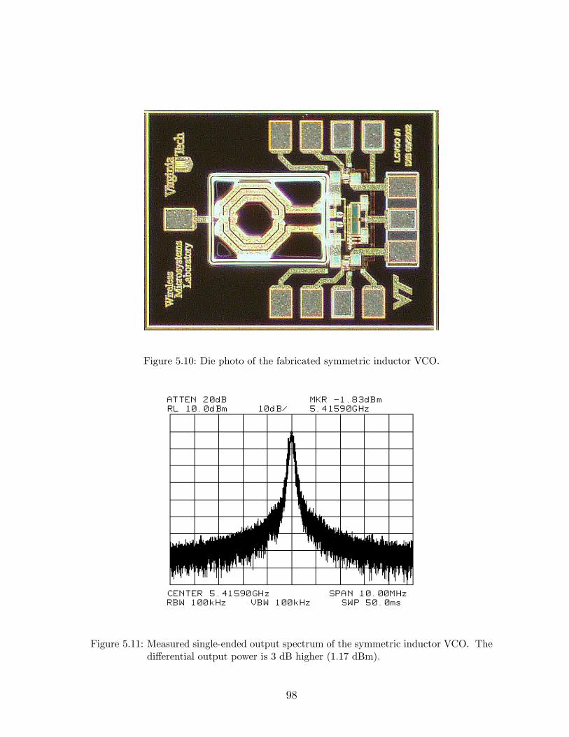
Figure 5.10: Die photo of the fabricated symmetric inductor VCO.
Figure 5.11: Measured single-ended output spectrum of the symmetric inductor VCO. Thedifferential output power is 3 dB higher (1.17 dBm).
98

4.1
4.3
4.5
4.7
4.9
5.1
5.3
5.5
1.5 2 2.5 3 3.5 4
Tuning Voltage (V)
Freq
uenc
y (G
Hz)
Figure 5.12: Measured frequency tuning characteristic of the symmetric inductor VCO.
Agilent E5500 phase noise measurement system. This phase noise system uses the
delay line method to downconvert the signal to baseband and measure the sideband
noise of the VCO [74]. Figure 5.13 shows the measured phase-noise spectrum of the
symmetric inductor VCO for a tank varactor control voltage of 0 V. At a 1 MHz
offset the measured phase noise is −112 dBc/Hz. This exceeds the −107 dBc/Hz ata 1 MHz offset specification for the IEEE 802.11a standard [20]. There appears to be
a spur in all the phase noise measurements of the symmetric inductor VCO at about
a 30 kHz offset, possibly from the measurement system or from an external interferer
coupling into the VCO. It is not believed that this bend in the phase noise is inherent
to the oscillator. Nevertheless, the results at a 1 MHz offset are not affected by this
apparent spur, and are, therefore, believed to be accurate.
However, the phase noise varies with different varactor control voltages. The mini-
mum phase noise of the symmetric inductor VCO (−115.5 dBc/Hz at a 1 MHz offset)occurs for a control voltage of 1.0 V (Figure 5.14). Figure 5.15 shows a plot of
the measured phase noise at a 1 MHz offset for varactor control voltages from 0 to 3
V. In general, the phase noise increases when the tuning characteristic of the tank
varactor is the sharpest. At this point the VCO has the highest tuning gain and is,
therefore, more susceptible to noise in the control voltage.
99

Figure 5.13: Measured phase noise spectrum of the symmetric inductor VCO with a tankcontrol voltage of 0 V.
Figure 5.14: The best measured phase noise spectrum of the symmetric inductor VCO. Thetank varactor control voltage is 1.0 V.
100
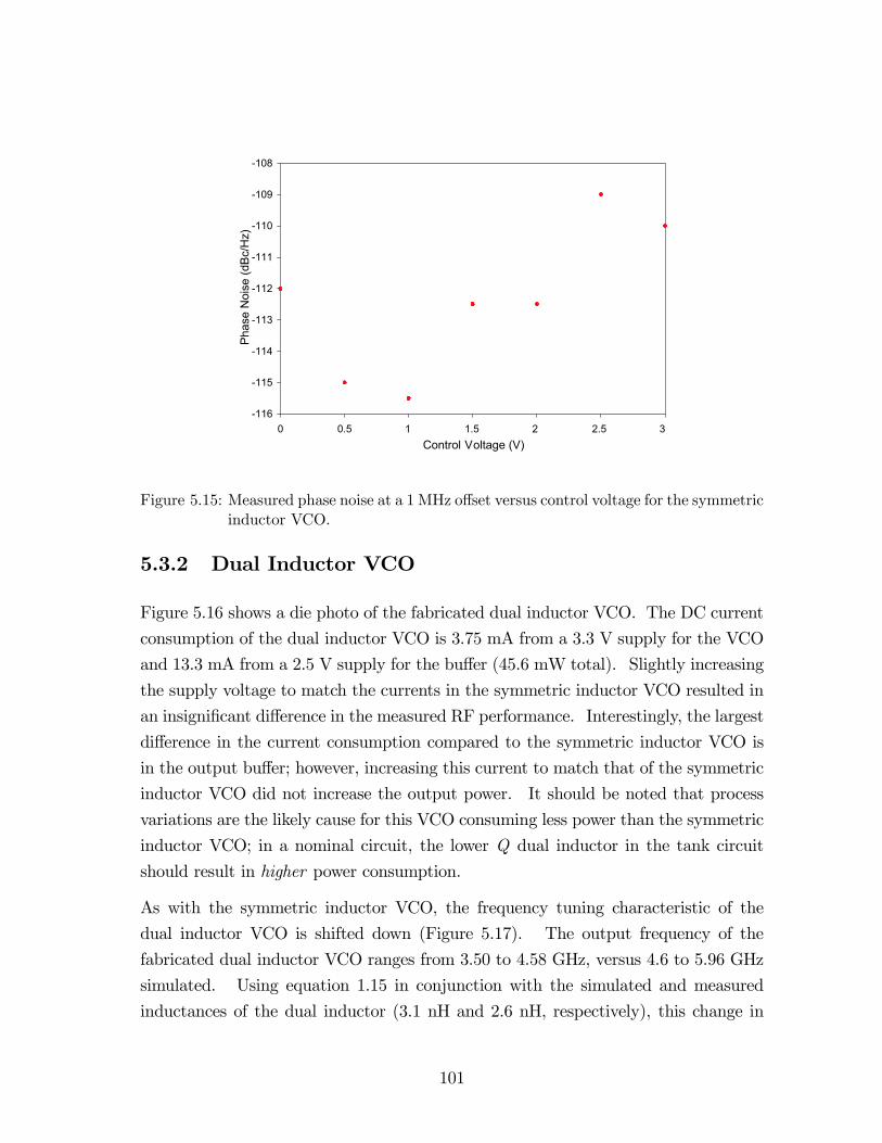
-116
-115
-114
-113
-112
-111
-110
-109
-108
0 0.5 1 1.5 2 2.5 3 Control Voltage (V)
P h a s
e N
o i s e
(d Bc
/Hz )
Figure 5.15: Measured phase noise at a 1 MHz offset versus control voltage for the symmetricinductor VCO.
5.3.2 Dual Inductor VCO
Figure 5.16 shows a die photo of the fabricated dual inductor VCO. The DC current
consumption of the dual inductor VCO is 3.75 mA from a 3.3 V supply for the VCO
and 13.3 mA from a 2.5 V supply for the buffer (45.6 mW total). Slightly increasing
the supply voltage to match the currents in the symmetric inductor VCO resulted in
an insignificant difference in the measured RF performance. Interestingly, the largest
difference in the current consumption compared to the symmetric inductor VCO is
in the output buffer; however, increasing this current to match that of the symmetric
inductor VCO did not increase the output power. It should be noted that process
variations are the likely cause for this VCO consuming less power than the symmetric
inductor VCO; in a nominal circuit, the lower Q dual inductor in the tank circuit
should result in higher power consumption.
As with the symmetric inductor VCO, the frequency tuning characteristic of the
dual inductor VCO is shifted down (Figure 5.17). The output frequency of the
fabricated dual inductor VCO ranges from 3.50 to 4.58 GHz, versus 4.6 to 5.96 GHz
simulated. Using equation 1.15 in conjunction with the simulated and measured
inductances of the dual inductor (3.1 nH and 2.6 nH, respectively), this change in
101
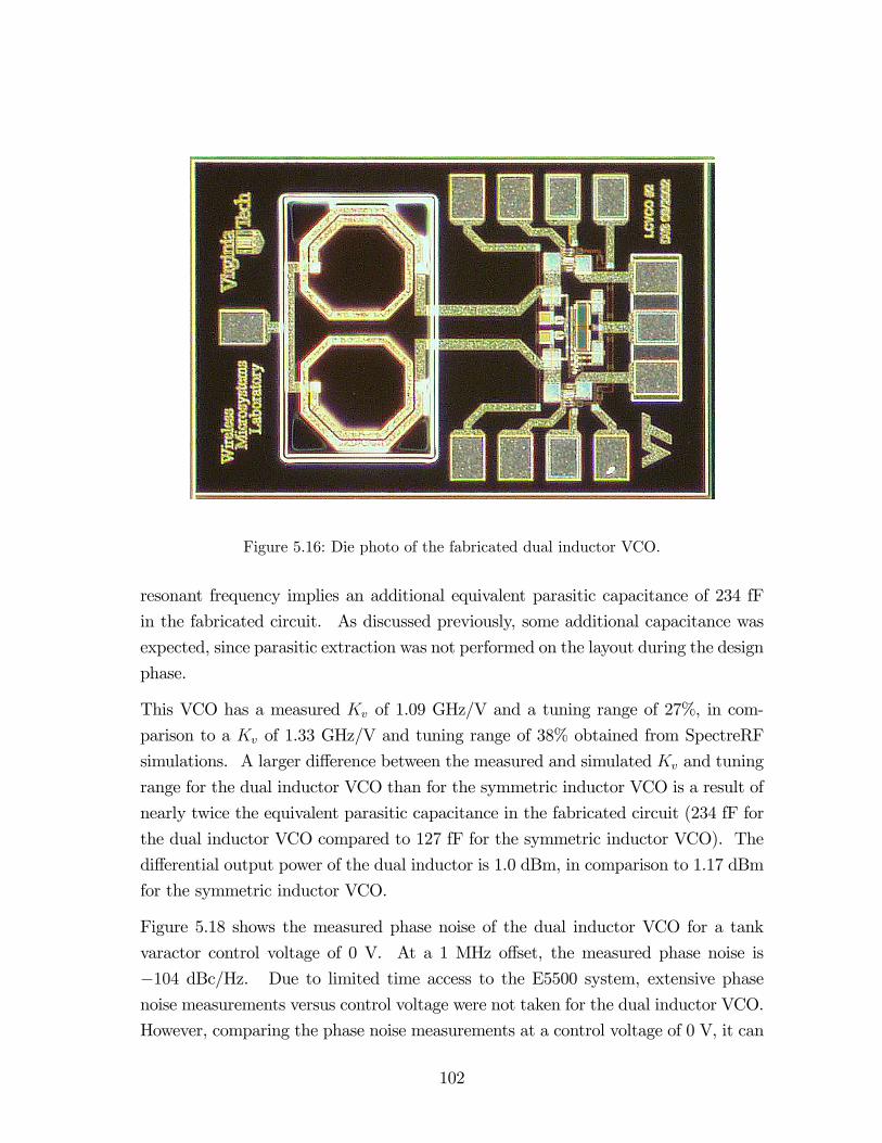
Figure 5.16: Die photo of the fabricated dual inductor VCO.
resonant frequency implies an additional equivalent parasitic capacitance of 234 fF
in the fabricated circuit. As discussed previously, some additional capacitance was
expected, since parasitic extraction was not performed on the layout during the design
phase.
This VCO has a measured Kv of 1.09 GHz/V and a tuning range of 27%, in com-
parison to a Kv of 1.33 GHz/V and tuning range of 38% obtained from SpectreRF
simulations. A larger difference between the measured and simulated Kv and tuning
range for the dual inductor VCO than for the symmetric inductor VCO is a result of
nearly twice the equivalent parasitic capacitance in the fabricated circuit (234 fF for
the dual inductor VCO compared to 127 fF for the symmetric inductor VCO). The
differential output power of the dual inductor is 1.0 dBm, in comparison to 1.17 dBm
for the symmetric inductor VCO.
Figure 5.18 shows the measured phase noise of the dual inductor VCO for a tank
varactor control voltage of 0 V. At a 1 MHz offset, the measured phase noise is
−104 dBc/Hz. Due to limited time access to the E5500 system, extensive phase
noise measurements versus control voltage were not taken for the dual inductor VCO.
However, comparing the phase noise measurements at a control voltage of 0 V, it can
102

3.4
3.6
3.8
4
4.2
4.4
4.6
4.8
1.5 2 2.5 3 3.5 4
Tuning Voltage (V)
Freq
uenc
y (G
Hz)
Figure 5.17: Measured frequency tuning characteristic of the dual inductor VCO.
Figure 5.18: Measured phase noise spectrum of the dual inductor VCO with a control volt-age of 0 V.
103

POUT IDC Phase Noise at RangeVCO (dBm) (mA) 1 MHz (dBc/Hz) (GHz)
Symmetric 1.17 3.81 −115.5 4.19− 5.45Dual 1.00 3.75 −104 3.50− 4.58
Table 5.1: Measured characteristics of the symmetric and dual VCOs. The DC currents arefor a supply of 3.3 V. The phase noise results are shown for tank varactor controlvoltages of 1.0 V for the symmetric inductor VCO and 0.0 V for the dual inductorVCO. The frequency tuning ranges are for tank varactor control voltages from1.5 to 4.0 V.
be seen that the dual inductor VCO has 8 dBc/Hz higher phase noise at a 1 MHz offset
then the symmetric inductor VCO (−112 dBc/Hz versus −104 dBc/Hz). The dualinductor VCO could potentially have a lower phase noise at higher control voltages
(as much as 3 dB lower), since the minimum phase noise of the symmetric inductor
VCO was measured at a control voltage of 1.0 V. Contrary to the SpectreRF PSS
simulations (Section 3.3), the measured phase noise results clearly show the benefit
of the higher Q tank circuit inductor in the symmetric inductor VCO. The measured
results of both the symmetric and dual inductor VCOs are summarized in Table 5.1.
5.4 Tunable Polyphase Measurements
The objective of the fabricated stand-alone tunable polyphase filter is a proof-of-
concept for the idea of using series output varactors to adjust the I/Q phase balance
of the polyphase outputs. In Chapter 4, the I/Q phase balance was specified by taking
the phase difference between neighboring curves in Figure 4.7. This results in four
phase balance terms, as illustrated in Figure 5.19(a). The tunable output polyphase
was introduced in Chapter 4 under the assumption that there was no differential phase
imbalance – in other words (I−)−(Q+) = (I+)−(Q−) and (Q−)−(I−) = (Q+)−(I+).Since this is a valid assumption for the unbuffered tunable polyphase, Section 4.3.1
refers to the I/Q phase errors as simply I and Q. However, it was shown later in
Chapter 4, that the input buffers introduce some differential phase imbalance to the
polyphase [Figure 5.19(b)]. Therefore, differential phase imbalance also exists in the
fabricated buffered polyphase. In this section, the four I/Q phase balance terms will
be expressed as (I−)− (Q+), (I+)− (Q−), (Q−)− (I−), and (Q+)− (I+).
104

I+I-
Q+
Q-
θ
θ
θ
θ
12
43
= (Q+) - (I+)
= (I+) - (Q-)
= (I-) - (Q+)
= (Q-) - (I-)
I-
I+
φ1
φ2
Q+
Q-
(a) (b)
Figure 5.19: Definition of (a) the four I/Q phase error angles and (b) the two differentialphase error angles.
During the design phase, the intended test setup for the polyphase incorporated a
balun between port 1 of the vector network analyzer (VNA) and the differential
input of the polyphase (Figure 5.20). Each of the outputs of the polyphase filter is
then sequentially connected to port 2 of the VNA, while the other three outputs are
terminated with DC blocks and 50 Ω loads. Thus, four separate S21 measurements
are required with this test setup to find the relative phase versus frequency at each
of the four polyphase outputs.
Unfortunately, the Anaren 30057 4-8 GHz balun used in this setup has an approximate
4 differential phase error over the 4.5 to 6.5 GHz bandwidth. This phase error
combines with the differential phase error in the input buffers to skew the relative
phase of the polyphase outputs. Without calibration, the effect of the differential
phase error from the input buffers of the polyphase and that of the balun itself are
indistinguishable.
The effect of the differential error at the input of the polyphase network on the output
phase is significant. Simulations of an ideal three-pole unbuffered polyphase filter
with a 0-176 differential input signal (i.e., −4 differential phase error) result in theoutput phase imbalance shown in Figure 5.21. While a perfectly balanced differential
input signal yields exact 0 I/Q phase error, the I/Q imbalance for a differential
105

HP 8510C Network Analyzer Display Module
HP8517B S-Parameter Test Set
3dB
3dB
50 Ω
Anaren 30057
HP 8510C Rack System
in-
in+
DC BIAS
Buffered Polyphase
Filter
DC Supply
I+
I-
Q+
Q-
50 Ω
50 Ω
50 Ω
DC block
DC block
DC block
DC block
Ref. Plane Ref. Plane
Σ
∆
Figure 5.20: Initial test setup of the stand alone polyphase using a balun at the input ofthe polyphase.
84
86
88
90
92
94
96
4.5 5 5.5 6 6.5 Frequency (GHz)
I /Q I m
b a l a
n c e
Im-Qp Ip-Qm Qm-Im Qp-Ip
Figure 5.21: Simulated I/Q phase imbalance of an ideal polyphase filter driven with a 0-176 differential signal (i.e., -4 differential phase error).
106

HP 8510C Network Analyzer Display Module
HP8517B S-Parameter Test Set
HP 8510C Rack System
50 Ω
in-
in+
DC BIAS
Buffered Polyphase
Filter
DC Supply
I+
I-
Q+
Q-
50 Ω
50 Ω
50 Ω
Ref. Plane Ref. Plane
DC block
DC block
DC block
DC block
Figure 5.22: “Single-ended” test setup for measurements of the standalone polyphase filtercircuit.
input phase error of 4 across the band from 4.5 to 6.5 GHz is approximately ±5.Accurately deembedding input phase error from the measurements can be done with
the measured S -parameter networks of the balun and polyphase filter. However,
since the differential input polyphase filter is actually a six-port S -parameter network,
deembedding the phase error from the test setup is far from trivial.
To avoid the problem with deembedding the phase error of the input balun, an alter-
nate test setup was used (shown in Figure 5.22). This test setup allows the polyphase
outputs to be effectively analyzed with a perfectly differential input signal. First,
four “single-ended” measurements are made with port 1 of the VNA connected to
the positive input of the polyphase and port 2 of the VNA connected to each one of
the four outputs sequentially. The negative input and the outputs of the polyphase
filter which are not connected to the VNA, are terminated with 50 Ω loads in order
to present the same terminations as the ports of the VNA. These four measure-
ments are repeated with port 1 of the VNA connected to the negative input of the
polyphase filter, and the positive input terminated in 50 Ω. Using superposition, the
effect of a perfectly differential signal is mathematically synthesized at the input of
107

Figure 5.23: Die photo of the fabricated standalone polyphase.
the polyphase by subtracting the phasor S21 measurements with port 1 of the VNA
connected to the negative input from the S21 measurements with port 1 of the VNA
connected to the positive input. The relative phases are obtained from the combined
S21 from these eight total measurements.
Figure 5.23 shows a die photo of the fabricated stand-alone polyphase. From a 2.5 V
supply, the polyphase input buffer consumes 13.74 mA (same as for the VCO output
buffers) and the output buffers consume 6.0 mA. The output buffers were designed
for a 1 kΩ termination, so the 50 Ω test equipment prevents the actual output power
of the polyphase from being measured correctly. However, the buffers prevent the
test equipment from loading down the polyphase itself, so the output phase tunability
can be accurately measured.
Measurements were taken for varactor control voltages ranging from 0 to 2.5 V. The
phase tunability is obtained by fixing two of the polyphase output varactor control
voltages (I or Q channel) while sweeping the other output varactor control voltages (Q
or I channel). For example, several measurements were taken by fixing the Vtune0 and
Vtune180 at 0 V and sweeping the Vtune90 and Vtune270 from 0 V to 2.5 V. The results
from one point in this sweep (Vtune0 = Vtune180 = 0 V and Vtune90 = Vtune270 = 2.5 V)
108

0
30
60
90
120
150
180
4.5 5 5.5 6 6.5
Frequency (GHz)
Phas
e Im
bala
nce
(I-)-(Q+) (I+)-(Q-)(Q-)-(I-) (Q+)-(I+)
Figure 5.24: Measured I/Q imbalance of the tunable polyphase for the case Vtune0 =Vtune180 = 0 V and Vtune90 = Vtune270 = 2.5 V.
are plotted in Figure 5.24 versus frequency. Recall that the polyphase was originally
designed to have poles at 5.15 GHz, 5.477 GHz, and 5.825 GHz. In the measurements
of this sample, it appears that the poles have been somewhat shifted up in frequency,
since the polyphase has a phase flatness from approximately 5.4 to 6.4 GHz, rather
than from 5.15 to 5.825 GHz. The upward shift in the poles could come as a result of
increased parasitic capacitance in the series combination of the output varactors and
the DC blocking capacitors at the input of the buffers. Decreased capacitance due
to series parasitics at the outputs could shift the pole frequencies upward. Process
variation in the capacitor dimensions could also be the cause for the shift in the phase
flatness bandwidth.
This sample of the stand-alone polyphase has an optimal measured ±5 phase flatnessbandwidth of 315 MHz, centered at 6.14 GHz (Figure 5.24). In simulation, the ±5phase flatness bandwidth is well over 2 GHz [Figure 4.10(b)]. However, a smaller
measured bandwidth is expected since parasitic resistances and capacitances of the
layout are not included in simulation. As previously shown in Figure 5.21, another
source of the limited bandwidth of the polyphase is differential imbalance in the
input buffers. It is likely that component mismatch in the input buffer introduces
109

(I+)-(I-)
160
165
170
175
180
185
190
195
5.1 5.3 5.5 5.7 5.9 6.1 6.3
Frequency (GHz)
Diff
eren
tial I
mba
lanc
e
I=0.0 Q=0.0
I=2.5 Q=0.0
I=0.0 Q=2.5I=2.5 Q=2.5I=0.5 Q=0.0
Figure 5.25: Measured differential phase error between the I+ and I− outputs of the tunablepolyphase.
differential error at the input of the polyphase, since the CMOS class-B buffer design
is not truly differential.
For the phase balance terms involving I+, there is a severe “kink” in the tuning
curves at approximately 5.65 GHz. The cause for this is seen by examining the
differential error in the I channel (Figure 5.25). At 5.65 GHz the difference between
the differential I+ and I− outputs has a similar kink. There are several potential
causes for this differential imbalance. First, the input buffers may be introducing
differential phase imbalance at the input of the polyphase that varies versus frequency.
The class-B CMOS buffer used at the polyphase input is not truly differential, so it
is more susceptible to component mismatch. However, one would not expect that
differential error at the input of the buffer alone would introduce a kink in the phase
in the I+ channel and not in any of the other channels. Second, there could be a
component mismatch or layout error within the polyphase filter itself that is only
affecting the poles of the I+ channel. Third, there could be a problem with the
I+ output bond wire, or other connections between the package and the network
analyzer, that is responsible for the kink in the phase around 5.65 GHz.
The tunability of the polyphase can be plotted at a fixed frequency versus the swept
110

82
84
86
88
90
92
94
96
98
0 0.5 1 1.5 2 2.5
Output Varactor Control Voltage (V)
I/Q Im
bala
nce
(I-)-(Q+) (I+)-(Q-)
(Q-)-(I-) (Q+)-(I+)
Figure 5.26: Measured I/Q imbalance at 6.14 GHz versus the output varactor control volt-age of Vtune90 and Vtune270. The Vtune0 and Vtune180 output varactor controlvoltages are fixed at 0 V.
output varactor control voltage. In Figure 5.24 it can be seen that the I/Q imbalances
all converge to 90 at approximately 6.14 GHz. I/Q imbalance data points at 6.14
GHz for a sweep of Vtune90 and Vtune270 from 0 V to 2.5 V are plotted in Figure 5.26.
At about 2.3 V, approximately 0 measured I/Q phase error for all four imbalance
terms is achieved. This plot also shows that the I/Q phase tunability is related to
the DC/small-signal C-V curve of the varactors.
A second sample of the stand-alone polyphase circuit was measured in order to inves-
tigate the cause for the kink in the I/Q phase angles and the frequency shift of the
poles observed in the first sample. The four measured I/Q phase imbalance angles of
the second sample are plotted at five distinct output varactor control voltage settings
and are overlaid in Figure 5.27. This figure shows the tunability of the phase flatness
bandwidth of the polyphase filter.
The kink at 5.65 GHz in the I/Q balance terms involving the I+ output of the first
sample does not occur within the bandwidth from 5.2 to 5.8 GHz for the second
sample. In general, the curves for this sample are much flatter within the bandwidth
specified by the design than the curves in Figure 5.24. The phase imbalance can
be tuned across approximately 15 for varactor control voltage settings from 0 to
111

(I-)-(Q+)
60
65
70
75
80
85
90
95
100
105
110
5.2 5.3 5.4 5.5 5.6 5.7 5.8 Frequency (GHz)
I /Q I m
b a l a
n c e
I=0.0 Q=2.5 I=0.5 Q=2.5 I=2.5 Q=2.5 I=2.5 Q=0.5 I=2.5 Q=0.0
(Q+)-(I+)
60
65
70
75
80
85
90
95
100
105
110
5.2 5.3 5.4 5.5 5.6 5.7 5.8Frequency (GHz)
I /Q I m
b a l a
n c e
I=0.0 Q=2.5 I=0.5 Q=2.5 I=2.5 Q=2.5 I=2.5 Q=0.5 I=2.5 Q=0.0
(I+)-(Q-)
70
75
80
85
90
95
100
105
110
115
120
5.2 5.3 5.4 5.5 5.6 5.7 5.8Frequency (GHz)
I /Q I m
b a l a
n c e
I=0.0 Q=2.5 I=0.5 Q=2.5 I=2.5 Q=2.5 I=2.5 Q=0.5 I=2.5 Q=0.0
(Q-)-(I-)
70
75
80
85
90
95
100
105
110
115
120
5.2 5.3 5.4 5.5 5.6 5.7 5.8 Frequency (GHz)
I /Q I m
b a l a
n c e
I=0.0 Q=2.5 I=0.5 Q=2.5 I=2.5 Q=2.5 I=2.5 Q=0.5 I=2.5 Q=0.0
(a) (b)
(c) (d)
Figure 5.27: Measured I/Q imbalance of the four output signals versus frequency and variousoutput varactor control voltages of a second polyphase circuit sample. Thefour I/Q phase imbalance terms are plotted separately: (a) (I−) − (Q+); (b)(Q+)− (I+); (c) (Q−)− (I−); and (I+)− (Q−).
112

2.5 V. Interestingly, the phase tunability in the fabricated circuit is nearly double
that predicted in simulation (15 measured versus 8 simulated). The cause for this
difference in measured and simulated data is still under investigation.
The upward frequency shift of the poles seen in Figure 5.24 is not present for this
sample. This implies that the shift of the poles in the first polyphase sample is
likely a result of a packaging error or smaller capacitor dimensions due to process
variations, rather than series parasitic capacitance, which would affect all the samples
in approximately the same way. However, a large (∼20), but relatively constant,differential error severely limits the ±5 phase flatness bandwidth of this sample. Toovercome this error, the four output varactor control voltages would need to be set
to four unique voltages. Due to the number of measurements and post-processing
mathematics required to determine I/Q phase balance, it would be very difficult to
optimize voltages with the current test setup. However, because of the flatness of
the curves, this sample offers the potential of having a ±5 phase flatness bandwidthof approximately 700 MHz, covering all three of the U-NII bands (5.15 to 5.825 GHz)
if the correct tuning voltages were found.
Extending the frequency range of Figure 5.27, a dramatic kink in the phase error
angles is observed at approximately 5.9 GHz, similar to the kink in band in the first
sample. Figure 5.28 shows this kink for the (I+)− (Q−) phase error angle. A similarkink occurs in all the other I/Q phase error angles at 5.9 GHz, as opposed to just
those involving the I+ output as in the first sample. Therefore, the source of the
kink in both samples is not likely to be an error in the design of the polyphase filter.
Process and/or packaging variations appear to have a large effect on what frequency
and range of phase error angles a kink may occur. Since the phase error introduced
by the buffers at the input of the polyphase cannot be measured independently, the
effect of phase imbalance in the buffers and shifted poles on the observed kink cannot
be specifically validated.
5.5 Summary
This chapter has presented measured data for the fabricated stand-alone inductor
test sites, symmetric inductor VCO, dual inductor VCO, and stand-alone tunable
113

(I+)-(Q-)
50
60
70
80
90
100
110
120
130
140
150
5.1 5.3 5.5 5.7 5.9 6.1 6.3
Frequency (GHz)
I/Q Im
bala
nce
I=0.0 Q=2.5I=0.5 Q=2.5I=2.5 Q=2.5I=2.5 Q=0.5I=2.5 Q=0.0
Figure 5.28: Measured (I+)−(Q−) imbalance over an extended frequency range to 6.3 GHz.
polyphase circuit. The symmetric inductor VCO core consumes 12.6 mW from a
3.3 V supply. Including buffers with a 2.5 V supply, the symmetric inductor VCO
consumes 47.8 mW, tunes from 4.19 to 5.45 GHz (Kv = 1.08 GHz/V in the linear
tuning region), and provides an output power of 1.17 dBm. From a 3.3 V supply,
the dual inductor VCO core consumes a comparable 12.4 mW. The buffered dual
inductor VCO consumes 45.6 mW, tunes from 3.50 to 4.58 GHz (Kv = 1.09 GHz/V
in the linear tuning region), and provides an output power of 1 dBm. For a tank
varactor control voltage of 1.0 V, the symmetric inductor VCO has a measured phase
noise of −115.5 dBc/Hz at a 1 MHz offset from the carrier. The dual inductor VCOhas a phase noise of −104 dBc/Hz at a 1 MHz offset for a control voltage of 0.0 V.The tunable polyphase consumes 13.74 mA in the input buffer and 6.29 mA in the
two output buffers from a 2.5 V supply (50.1 mW) and offers the potential for a
±5 phase flatness bandwidth of approximately 700 MHz centered at 5.5 GHz, if thecorrect output phase control voltages were obtained. Tunable output varactor control
voltages allow the fabricated circuit to tune through approximately 15 of I/Q phase
imbalance.
The combined symmetric inductor VCO with tunable polyphase outputs was dam-
114

aged by the vendor in the packaging process and has not yet been tested. Efforts are
underway to recover samples of this circuit from unsawed wafer sections. However,
the independently verified functionality of the VCO and tunable polyphase circuits
shows that the combined circuit would indeed result in a VCO with tunable polyphase
outputs. Incorporating tunable I/Q phase balance, therefore, requires only an addi-
tional 6 mA (for the polyphase output buffers) over what is required for the buffered
symmetric inductor VCO itself.
115

Chapter 6
Conclusions and Future Work
The primary objective of this work was to demonstrate the concept of a quadrature
LO source with analog tunable I/Q balance, which could potentially be used to im-
prove the bit-error-rate (BER) of an I/Q receiver or to improve the image rejection
ratio (IRR) of a Weaver receiver architecture. The independent demonstrations of
the symmetric inductor VCO and tunable polyphase presented in this thesis have ver-
ified the concept of a quadrature LO source with tunable I/Q phase balance. This
analog method to correct I/Q phase imbalance is the major contribution of this work,
and may have potential advantages in power consumption and speed compared to
DSP based solutions. In the course of this research, knowledge was gained in the de-
sign, modeling, and characterization of differential monolithic inductors, VCOs, and
polyphase circuits.
6.1 Conclusions
The I/Q balance tunability of a stand-alone polyphase filter was characterized in
terms of phase flatness bandwidth, phase tuning range, and power consumption.
First, the stand-alone polyphase offers the potential for a ±5 measured phase flat-ness bandwidth of 700 MHz versus a simulated bandwidth of over 2 GHz. The
smaller measured phase flatness bandwidth realized in practice is mainly a result of
the parasitic resistances and capacitances of the layout. These parasitics could not
be reliably extracted, so they were not accounted for in the design phase of this work.
116

Another source of the limited bandwidth of the polyphase is differential imbalance
in the input buffers, since the buffer design used was not truly differential. Any im-
balance at the input of the polyphase network reduces the phase flatness bandwidth
substantially. Also, the bandwidth of the fabricated polyphase is shifted upward
in frequency from the simulated design. Process variation resulting in smaller pole
capacitance or packaging variations in the stand-alone polyphase is the likely cause
for an upward frequency shift of the poles in the fabricated circuit, since the shift was
not consistently observed in every sample. Second, the measured phase tuning range
of the polyphase is approximately 15, though only 8 was predicted in simulation.
Though this phase tunability would be sufficient to attain ±5 phase flatness acrossthe 5.15 to 5.825 GHz bandwidth of the polyphase filter, the post-processing mathe-
matics required to determine the I/Q phase balance make it very difficult to determine
the appropriate output varactor control voltages. Finally, the phase tunability comes
at the expense of only approximately 6 mA additional current consumption (due to
the polyphase output buffers) over that consumed in the buffered VCO alone. The
combined VCO and polyphase current consumption is potentially much less than what
would be needed for I/Q phase correction using DSP-based techniques and possibly
avoids latency issues.
Based on the measured results of the phase flatness bandwidth, phase tuning range,
and power consumption for the fabricated circuit, the ability to tune I/Q balance
at RF is quite feasible, particularly if corrections are made to improve the design of
the polyphase network developed in this work. Efforts to improve differential phase
balance in the input buffers would increase the phase flatness bandwidth and allow
the tunable polyphase to correct for or introduce a greater range of I/Q phase imbal-
ance. Moreover, the overall current consumption could be decreased by improving
the output buffer of the VCO (input buffer of the polyphase).
Two differential inductors were designed and characterized in this work. The first
is an electrically symmetric inductor and the second is the classical dual inductor
structure. The inductors were measured with an on-wafer probe station to obtain the
differential effective inductance and Q factor. At 5.25 GHz, the symmetric inductor
has an effective inductance of 2.2 nH and Q factor of 15.4, whereas the dual inductor
has an effective inductance of 2.6 nH and a Q factor of 10.4. Thus, the electrically
symmetric inductor offers an approximate 48% improvement in Q factor over the dual
117

inductor structure at this frequency.
Several of the design goals for the symmetric inductor VCO obtained in simulation
were met in practice. The phase noise for all varactor control voltages exceeds the
phase noise specification for IEEE 802.11a of −107 dBc/Hz at a 1 MHz offset fromthe carrier. The best case phase noise measurement (−115.5 dBc/Hz at a 1 MHzoffset) occurs for a tank varactor control voltage of 1.0 V. In addition, the 4.19 to
5.45 GHz tuning range covers the lower U-NII bands from 5.15 to 5.35 GHz, making
the symmetric inductor VCO limitedly useful for direct conversion or low-IF receiver
applications in this frequency regime. This VCO is not desirable for PLL applications
due to a highKv; however, the intended application of this VCO is to drive the tunable
polyphase filter, which does not require low Kv. Another limitation of this VCO is
that it does not cover the upper 100 MHz band from 5.725 to 5.825 GHz; however,
this can be corrected by a revision which compensates for parasitics. The measured
output power of the symmetric inductor VCO 1.17 dBm.
In comparison, the measured phase noise of the dual inductor VCO is −104 dBc/Hzat a 1 MHz offset (at a varactor control voltage of 0.0 V) – approximately 8 dBc/Hz
worse than that of the symmetric inductor VCO at the same varactor control voltage
(−112 dBc/Hz). A 48% lower measured Q factor for the tank inductor in this VCO
compared to the symmetric inductor leads to the lower phase noise measurement. In
addition, the highest output frequency of the dual inductor VCO is 650 MHz below
the lower limit of the U-NII band (5.15 GHz). This makes the dual inductor VCO
(as realized) unusable for direct conversion and low-IF receivers in the U-NII bands,
though it provided a very useful comparison with the symmetric inductor VCO.
A widely accepted figure-of-merit (FOM) for VCOs is given by [75]:
FOM = L (∆ω)− 20 log³ ω0∆ω
´+ 10 log
µPdiss
1 mW
¶(6.1)
This FOM normalizes the phase noise at a given offset, the center frequency, and
the power consumption in milliwatts. The FOM of the symmetric inductor VCO is
−179.2 dBc/Hz, which compares well with the best reported VCO FOM in the 5 GHz
frequency regime of −183.6 dBc/Hz [76]. Figure 6.1 plots the FOMs of several com-parable 5 GHz VCOs over the past four years [77],[78],[79],[80],[81],[82],[83],[84],[85].
118

-185
-180
-175
-170
-165
-160
-155
1997 1998 1999 2000 2001 2002 2003 2004
Year
Figu
re-o
f-Mer
it (d
Bc/H
z)
[Symm]
[Dual]
[76]
[77][78]
[79]
[80]
[81][82]
[83]
[84]
[85]
Figure 6.1: Comparison of the figure-of-merit from several VCOs over the past four yearswith the VCOs of this work.
The advantage of the higher Q symmetric inductor is quantified by comparing the
FOM of the two VCO designs at the same varactor control voltage of 0 V. At this
tuning voltage, the dual inductor VCO FOM is −166.3 dBc/Hz compared to −175.7dBc/Hz for the symmetric inductor VCO – an improvement of about 10 dBc/Hz.
6.2 Improvements and Future Work
This section discusses several improvements that could be made in future revisions
the circuits of this work as well as potential future work that could be done in the
area of tunable I/Q LO sources.
• The inductor measurements could be improved by including open and shortstandards for the pads in any future revisions. It is expected that the measured
data agrees more closely to the full-wave electromagnetic simulations performed
than shown by the comparisons presented in Section 5.2, since simulated data
was used to deembed the probe pad parasitics. More accurate deembedding
standards would likely improve the correlation of measured Q factor with the
electromagnetic simulations at higher frequencies.
119

• Future revisions of the VCOs would benefit from redesigning the tank circuit toaccount for parasitic capacitance so that the output frequency range would cover
all three of the U-NII bands from 5.15 to 5.825 GHz. It should be noted that
first pass success of an RFIC requires accurate and reliable parasitic extraction
for the given process. A revised design could also include modifying the tank
circuit with fixed switched capacitance and smaller varactors in order to lower
the effective Kv of the VCOs. Both the VCO designs would benefit from lower
Kv so that they could be integrated into phase locked loops (PLLs).
• The VCO design could be improved, as discussed in Chapter 3, by using a
capacitive divider to attenuate the output of the VCO to avoid compressing
a classical differential pair buffer at the output. This would not affect VCO
phase noise, since the VCO core is allowed to operate with a high oscillation
amplitude – the attenuation would primarily improve power consumption in
the output buffers. However, if a differential pair were to be used, the input
impedance of the polyphase would need to be increased to prevent loading down
the output of the buffer and degrading the gain.
• Future work also includes testing the fabricated tunable polyphase VCO circuitsthat were damaged by the vendor in the packaging process. A die photo of
this polyphase VCO is shown in Figure 6.2. Efforts are currently underway to
package and test samples of this circuit from a previously unsawed wafer section.
When the circuits are available for testing, a different test setup will be required
than that used for the stand-alone polyphase filter. For example, the circuit
could be tested by mixing down the quadrature phase outputs to a frequency
that could be sampled by an oscilloscope in the time domain (e.g., less than
100 MHz) (see Figure 6.3). After downconversion, the output signals could
be analyzed for various varactor control voltages as in Section 5.4. However,
all the downconversion mixers would need to provide the same relative phase
shift to each of the IF outputs to the oscilloscope for this test setup, unless the
mixers were calibrated out of the measurements.
• The quadrature VCO with tunable polyphase outputs would benefit from a re-vision of the symmetric inductor VCO to increase its output frequency range.
A similar revision is needed to reduce the differential error introduced to the
120

Figure 6.2: Die photo of the polyphase VCO with tunable I/Q phase balance.
DC BIAS
Combination Polyphase
VCO
DC Supply
I+
I-
Q+
Q-
1 MΩ
DC block
DC block
DC block
DC block
1 MΩ 1 MΩ 1 MΩ
Agilent 54624A Oscilloscope
f LO
Figure 6.3: Potential test setup for the polyphase VCO circuit.
121

polyphase circuit by its input buffer (i.e., the VCO output buffer). Such a revi-
sion would need to increase the ±5 phase flatness bandwidth of the polyphasenetwork and simplify tuning the polyphase output varactor control voltages for
minimum phase error.
• Since the concept of a polyphase with tunable I/Q balance has been demon-
strated, a method to sense the output I/Q imbalance and automatically adjust
the output varactor control voltages is required in order to integrate a tunable
I/Q LO source into a receiver. Using the tunable polyphase in a Weaver ar-
chitecture would require sensing the required I/Q imbalance to intentionally
introduce the phase compensation at the outputs to improve image rejection.
To improve the BER of an I/Q receiver (e.g., direct conversion and low-IF re-
ceivers), a method to detect I/Q imbalance would be required. One potential
solution is to use a variation of a phase-locked loop with multiple phase detec-
tors to create control voltages for the polyphase output varactors. The feedback
required for any automatic control of the phase tunability would introduce la-
tency into the system, and this would need to be compared with the equivalent
delay for competing DSP-based solutions.
122

Appendix A
Derivation of Inductor Parameters
As discussed in Chapter 2, a monolithic inductor on lossy Si substrates can be modeled
by the lumped element network shown in Figure A.1. Furthermore, by assuming
that Y12 = Y21, the lumped elements can be combined into a π-equivalent circuit of
admittance blocks (Figure A.2).
Single-ended excitation requires that port 2 of the inductor be grounded. Thus, the
Y22 + Y12 element of Figure A.2(a) is shorted out, reducing the input impedance to:
R+ jX =1
Y11 + Y12 − Y12=
1
Y11(A.1)
Therefore, the single ended equivalent inductance and Q factor are given by:
L =X
2πf=
1
2πf· Im (1/Y11) (A.2)
and
Q =X
R=Im(1/Y11)
Re (1/Y11). (A.3)
However, if the inductor is to be used differentially, the floating impedance between
the two ports of the π-equivalent circuit in Figure A.2(b) must be used to calculate
the equivalent inductance and Q factor. By inspection, this floating impedance is
given as the parallel combination of the series admittance (−Y12) and the sum of thetwo shunt elements (Y11 + Y12 and Y22 + Y12) [51]. This floating impedance can be
123
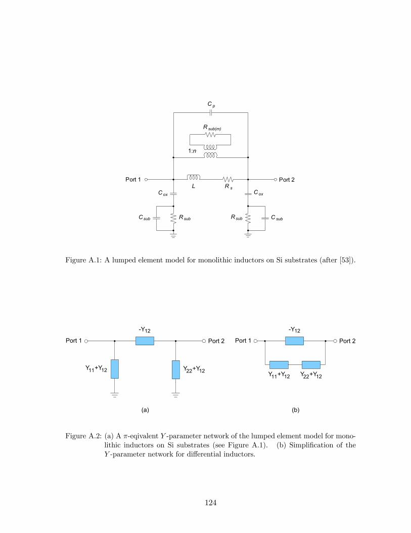
L RCox
C p
R sub(m)
Rsub C sub
Port 1 Port 2
RsubCsub
Coxs
1:n
Figure A.1: A lumped element model for monolithic inductors on Si substrates (after [53]).
-Y12
Y +Y 1211 Y +Y 1222
Port 1 Port 2
-Y12
Y +Y 1211 Y +Y 1222
Port 1 Port 2
(a) (b)
Figure A.2: (a) A π-eqivalent Y -parameter network of the lumped element model for mono-lithic inductors on Si substrates (see Figure A.1). (b) Simplification of theY -parameter network for differential inductors.
124

simplified in several steps:
R+ jX =
µ− 1
Y12
¶kµ
1
Y11 + Y12+
1
Y22 + Y12
¶(A.4a)
=− 1
Y12
³1
Y11+Y12+ 1
Y22+Y12
´− 1
Y12+ 1
Y11+Y12+ 1
Y22+Y12
(A.4b)
=
Y22+Y11+2Y12−Y12(Y11+Y12)(Y11+Y12)
(Y11+Y12)(Y22+Y12)−Y12(Y22+Y12)−Y12(Y11+Y12)−Y12(Y11+Y12)(Y11+Y12)
(A.4c)
=Y22 + Y11 + 2Y12
(Y11 + Y12) (Y22 + Y12)− Y12 (Y22 + Y12)− Y12 (Y11 + Y12)(A.4d)
=Y22 + Y11 + 2Y12
Y11Y22 + Y11Y12 + Y22Y12 + Y 212 − Y12Y22 − Y 2
12 − Y12Y11 − Y 212
(A.4e)
=Y22 + Y11 + 2Y12Y11Y22 − Y 2
12
. (A.4f)
This simplified equation can be used to calculate the differential equivalent inductance
and Q factor:
L =X
2πf=
µ1
2πf
¶·Im
µY11 + Y22 + 2Y12Y11Y22 − Y 2
12
¶¸(A.5)
and
Q =X
R=
hIm³Y11+Y22+2Y12Y11Y22−Y 212
´ihRe³Y11+Y22+2Y12Y11Y22−Y 212
´i . (A.6)
Equations A.5 and A.6 were used in this work to characterize the differential inductors
used in the symmetric and dual VCO tank circuits.
125

Appendix B
Derivation of the PolyphaseTransfer Function
Figure B.1(a) shows a single-stage RC -CR network. Using the V2,in node as the
reference, the V1,in to V1,out voltage transfer function is given by:
F11 (ω) =V1,outV1,in
=1
1 + jωRC(B.1)
and the V1,in to V2,out voltage transfer function is given by:
F21 (ω) =V2,outV1,in
=−jωRC1 + jωRC
. (B.2)
The phase angle of these two transfer functions are:
∠F11 (ω) = − tan−1 (ωRC) (B.3)
∠F21 (ω) = 90 − tan−1 (ωRC) . (B.4)
From these two equations, it follows that the two outputs always differ in phase by
90. In particular, when ω = 1/RC, the phase shift of V1,out is −45 and the phaseshift of V1,out is +45.
126

V2,in
V1,in
V4,in
V3,in
V2,out
V1,out
V4,out
V3,out
RC
RC
RC
RC
V2,in
V1,in
V2,out
V1,outRC
RC
(a) (b)
Figure B.1: Schematics of (a) a two-phase RC -CR network and (b) a four-phase RC -CRnetwork.
Using equations B.1 and B.2, the transfer matrix of this network is given by:"V1,out
V2,out
#=
1
1 + jωRC
"1 jωRC
−jωRC 1
#"V1,in
V2,in
#. (B.5)
The sign difference of the jωRC elements of the matrix is necessary because the
transfer equations depend on the polarity of the input signals with respect to the
output signals. The transfer matrix is circulant and, therefore, the network can be
classified as a Hilbert filter [86],[70],[87].
If a positive complex input signal is defined as Vin = V1,in + jV2,in (i.e., a +90
phase difference as in equations B.3 and B.4), the open-circuit transfer function of
the RC -CR circuit is given by:
G+ (ω) =1
2F11 (ω) +
1
2F22 (ω)− 1
2jF12 (ω) +
1
2jF21 (ω) =
1 + ωRC
1 + jωRC(B.6)
where the complex number (±j) included with F12(ω) and F21(ω) is necessary becauseof the polarity of the complex input signal. The factor of 1/2 is necessary to account
for the differential to single-ended conversion to find the transfer function. Similarly,
the open-circuit transfer function of the RC -CR circuit when Vin = V1,in − jV2,in (a
127

−90 phase difference or negative input sequence) is given by:
G− (ω) =1
2F11 (ω) +
1
2F22 (ω) +
1
2jF12 (ω)− 1
2jF21 (ω) =
1− ωRC
1 + jωRC(B.7)
Therefore, the phase response of the complex output depends on the polarity of the
input sequence, and is given by:
∠G+ (ω) = − tan−1 (ωRC) (B.8)
∠G− (ω) = −180 − tan−1 (ωRC) . (B.9)
A relationship between the complex output phase and the individual output phases
can be determined by comparing equations B.8 and B.9 with equations B.3 and B.4.
First, the output phase of the differential V1,out signal can be found using equation
B.8 or B.9, depending on the polarity of the input signal. Second, the output phase
of the differential V2,out signal can be found by adding 90 to equation B.8 or B.9.
The differential input and output signals of the polyphase network shown in Figure
B.1(b) can be defined as:
VI,in = V1,in − V3,in (B.10)
VQ,in = V2,in − V4,in (B.11)
VI,out = V1,out − V3,out (B.12)
VQ,out = V2,out − V4,out (B.13)
These differential signals allow the single stage polyphase network to be described
using the same transfer matrix as the RC -CR network given in equation B.5:"VI,out
VQ,out
#=
1
1 + jωRC
"1 jωRC
−jωRC 1
#"VI,in
VQ,in
#. (B.14)
As with the RC -CR network, for positive input sequences, the open-circuit transfer
function of a single-stage polyphase network is given by:
G+1 (ω) =
1 + ωRC
1 + jωRC. (B.15)
128

and for negative input sequences:
G−1 (ω) =1− ωRC
1 + jωRC. (B.16)
Similarly, the output phase response for differential complex positive and negative
sequences are again given by:
∠G+1 (ω) = − tan−1 (ωRC) (B.17)
∠G−1 (ω) = −180 − tan−1 (−ωRC) . (B.18)
However, for quadrature signal generation, the individual phases of the V1,out, V2,out,
V3,out, and V4,out nodes are of greater importance. Using equations B.3, B.4, and
B.17, the phase angles of V1,out and V2,out are:
∠V1,out = − tan−1 (ωRC) (B.19)
∠V2,out = 90 − tan−1 (ωRC) . (B.20)
From equations B.3, B.4, and B.18 the phase angles of V3,out and V4,out are:
∠V3,out = −180 − tan−1 (ωRC) (B.21)
∠V4,out = −90 − tan−1 (ωRC) . (B.22)
These four equations show the quadrature phase generation created by the polyphase
network from a differential input signal.
The transfer function of multiple stage networks are found by simplifying a series
connection of single-stage polyphase transfer functions (i.e., equation B.15). For
example, the transfer function of a three-pole polyphase network is given by [86]:
G3 (ω) = G+1,1 (ω)G
+1,2 (ω)G
+1,3 (ω) =
N3 (ω)
D3R (ω) + jD3I (ω)(B.23)
where
N3 (ω) = (1 + ωR1C1) (1 + ωR2C2) (1 + ωR3C3) (B.24)
129

D3R (ω) = 1− ω2[R1C1R2C2 +R2C2R3C3 +R1C1R3C3
+2R1C3 (R2C2 +R2C1 +R3C2)] (B.25)
D3I (ω) = ω [R1C1 +R2C2 +R3C3 + 2 (R1C2 +R2C3 +R1C3)]
−ω3R1C1R2C2R3C3. (B.26)
The polyphase designed in this thesis has a transfer function represented by equation
B.23. The gain and phase of this transfer function are given by [86]:
|G3 (ω)| = |N3 (ω)|q[D3R (ω)]
2 + [jD3I (ω)]2
(B.27)
∠G3 (ω) = − tan−1µD3I (ω)
D3R (ω)
¶(B.28)
130

Appendix C
Matlab Code for CalculatingDifferential Inductor Parameters
C.1 l_extract.m
function [f,Z,L,Q]=l_extract(sfile)
%l_extract imports the S-parameters from a real/imaginary touchstone
% formatted file, converts to Y-parameters and calculates the differential
% effective inductance and Quality (Q) factor.
% [f,Z,L,Q]=l_extract(sfile) where:
% sfile := the absolute or relative path to touchstone format input file
% f := a vector containing the frequency points
% Z := a vector of the impedance (complex numbers)
% L := a vector of the differential effective inductance (nH)
% Q := a vector of the differential Quality factor
%
% read all the data from comma separated ASCII files, real-imag format
[f,s11,s21,s12,s22]=readTouch(2,sfile);
% change units to GHz and nH
f=f/1e9;
%
fig=0;
131

%
% convert s-parameters to y-parameters
z0=50;
y0=z0^-1;
den=(1+s11).*(1+s22)-(s12.*s21);
y11=y0*(((1-s11).*(1+s22)+(s12.*s21))./den);
y22=y0*(((1+s11).*(1-s22)+(s12.*s21))./den);
y12=y0*((-2*s12)./den);
y21=y0*((-2*s21)./den);
%
% Calculate Inductor parameters
Z=(y11+y22+y12+y21)./(y11.*y22-y12.*y21);
L=imag((Z)./(2*pi*f));
L1=imag((1./-y12)./(2*pi*f));
Q=(imag(Z)./real(Z));
Q1=imag(1./-y12)./real(1./-y12);
%
% Plot Results
% Inductance
fig=fig+1;
figure(fig), plot(f,L,f,L1)
title(’Differential Inductance’);
ylabel(’Inductance’), xlabel(’frequency (Hz)’)
% Quality Factor
fig=fig+1;
figure(fig), plot(f,Q,f,Q1)
title(’Differential Quality Factor (Q)’);
ylabel(’Q’), xlabel(’frequency (Hz)’)
% Impedance
fig=fig+1;
figure(fig), plot(f,real(Z),f,imag(Z))
title(’Floating Impedance’);
ylabel(’impedance (ohms)’), xlabel(’frequency (Hz)’)
legend(’real’,’imaginary’)
132

C.2 readTouch.m
function [f,s11,s21,s12,s22]=readTouch(portnum,file1)
%readTouch imports S-parameters from a touchstone formatted file
% and outputs the frequency and S-parameters in separate vectors.
% [f,s11,s21,s12,s22]=readTouch(portnum,file1) where:
% portnum := number of ports (1 or 2)
% file1 := the absolute or relative path to touchstone format input file
% f := a vector containing the frequency points
% s11 := a vector containing s11 (complex numbers)
% s21 := a vector containing s21 (complex numbers)
% s12 := a vector containing s12 (complex numbers)
% s22 := a vector containing s22 (complex numbers)
%
% Open input file
sdata = fopen(file1,’r’); % Open input file
% Ignore comment lines
n=0;
freqUnit=1e9; % set default frequency unit to GHz
while n==0
s = fgetl(sdata);
P = sscanf(s,’%s’);
if P(1)==’!’
n=0;
elseif P(1)==’#’
% test for frequncy unit
if P(2)==’G’ | P(2)==’g’ % GHzfreqUnit=1e9;
elseif P(2)==’M’ | P(2)==’m’ % MHzfreqUnit=1e6;
elseif P(2)==’K’ | P(2)==’k’ % kHz
133

freqUnit=1e3;
else % Hz
freqUnit=1;
P(6)=P(5);
end
% test for complex number format
if P(6)==’M’ | P(6)==’m’n=1; % format is magnitude angle
else
n=2; % format is real imaginary
end
else
output=sprintf(’\n"%s" is not in Touchstone format.\n’,file1);disp(output);
n=2;
end
end
if n==1 % Magnitude angle file
notEOF=feof(sdata);
n=1;
while notEOF==0
deg2rad=pi/180;
s = fgetl(sdata);
notEOF=feof(sdata);
if (portnum==1)
% Read 3 columns of the next row to vector P
P = sscanf(s,’%s’)’;
if P(1)~=’!’
P = sscanf(s,’%g %g %g’)’;
f(n)=P(1)*freqUnit;
s11(n)=P(2)*cos(P(3)*deg2rad)+i*P(2)*sin(P(3)*deg2rad);
n=n+1;
end
elseif (portnum == 2)
134

% Read 9 columns of the next row to vector P
P = sscanf(s,’%s’)’;
if P(1)~=’!’
P = sscanf(s,’%g %g %g %g %g %g %g %g %g’)’;
f(n)=P(1)*freqUnit;
s11(n)=P(2)*cos(P(3)*deg2rad)+i*P(2)*sin(P(3)*deg2rad);
s21(n)=P(4)*cos(P(5)*deg2rad)+i*P(4)*sin(P(5)*deg2rad);
s12(n)=P(6)*cos(P(7)*deg2rad)+i*P(6)*sin(P(7)*deg2rad);
s22(n)=P(8)*cos(P(9)*deg2rad)+i*P(8)*sin(P(9)*deg2rad);
n=n+1;
end
else
output=sprintf(’\nOnly one or two port networks supported at this time.’);disp(output);
notEOF=2;
end % if portnum==1
end % while loop
end
if n==2 % Real Imaginary file
notEOF=feof(sdata);
n=1;
while notEOF==0
s = fgetl(sdata);
notEOF=feof(sdata);
if (portnum==1)
% Read 3 columns of the next row to vector P
P = sscanf(s,’%s’)’;
if P(1)~=’!’
P = sscanf(s,’%g %g %g’)’;
f(n)=P(1)*freqUnit;
s11(n)=P(2)+i*P(3);
n=n+1;
end
elseif (portnum == 2)
135

% Read 9 columns of the next row to vector P
P = sscanf(s,’%s’)’;
if P(1)~=’!’
P = sscanf(s,’%g %g %g %g %g %g %g %g %g’)’;
f(n)=P(1)*freqUnit;
s11(n)=P(2)+i*P(3);
s21(n)=P(4)+i*P(5);
s12(n)=P(6)+i*P(7);
s22(n)=P(8)+i*P(9);
n=n+1;
end
else
output=sprintf(’\nOnly one or two port networks supported at this time.’);disp(output);
notEOF=2;
end % if portnum==1
end % end while
end
fclose(sdata);
136

Bibliography
[1] W. Webb, “From ‘cellphone’ to ‘remote control on life’: How wireless communi-
cations will change the way we live over the next 20 years,” in 2002 IEEE RFIC
Symposium Digest, June 2002, pp. 7—11.
[2] G.E. Moore, “Cramming more circuits onto integrated circuits,” Proceedings of
the IEEE, vol. 86, no. 1, pp. 82—85, Jan. 1998.
[3] J. Crols and M.S.J. Steyaert, “Low-IF topologies for high-performance analog
front ends of fully integrated receivers,” IEEE Transactions on Circuits and
Systems—II: Analog and Digital Signal Processing, vol. 45, no. 3, pp. 269—282,
Mar. 1998.
[4] A. Mashhour, W. Domino, and N. Beamish, “On the direct conversion receiver
— a tutorial,” Microwave Journal, vol. 44, no. 6, pp. 114—128, June 2001.
[5] A. Loke and F. Ali, “Direct conversion radio for digital mobile phones — de-
sign issues, status, and trends,” IEEE Transactions on Microwave Theory and
Techniques, vol. 50, no. 11, pp. 2422—2435, Nov. 2002.
[6] A. Matsuzawa, “RF-SoC — expectations and required conditions,” IEEE Trans-
actions on Microwave Theory and Techniques, vol. 50, no. 1, pp. 245—253, Jan.
2002.
[7] R. Svitek, and S. Raman, “A SiGe active sub-harmonic front-end for 5-6 GHz
direct conversion receiver applications,” to be published in 2003 IEEE RFIC
Symposium Digest, June 2003.
[8] S. Chakraborty, S.K. Reynolds, T. Beukema, H. Ainspan, and J. Laskar, “Ar-
chitectural trade-offs for SiGe BiCMOS direct conversion receiver front-ends for
137

IEEE 802.11a,” in 2002 IEEE Gallium Arsenide Integrated Circuit (GaAs IC)
Symposium Digest, 2002, pp. 120—123.
[9] C.-W. Wu, M.-C. Su, P.-S Hsiao, K.-P. Lan, and K.Y.-J. Hsu, “A direct-
conversion CMOS receiver for 5 GHz wireless LAN,” in 2002 IEEE Asia-Pacific
Conference on ASIC Proceedings, 2002, pp. 311—314.
[10] B. Razavi, RF Microelectronics, Prentice-Hall, Englewood Cliffs, NJ, 1997.
[11] B. Razavi, “Design considerations for direct-conversion receivers,” IEEE Trans-
actions on Circuits and Systems—II: Analog and Digital Signal Processing, vol.
44, no. 6, pp. 428—435, June 1997.
[12] E. Cetin, I. Kale, and R.C.S. Morling, “On the performance of a blind source
separation based I/Q-corrector,” in 2002 IEEE Radio and Wireless Conference
(RAWCON), 2002, pp. 99—102.
[13] A. Schuchert, R. Hasholzner, and P. Antoine, “A novel IQ imbalance com-
pensation scheme for the reception of OFDM signals,” IEEE Transactions on
Consumer Electronics, vol. 47, no. 3, pp. 313—318, Aug. 2001.
[14] M. Valkama and M. Renfors, “Advanced DSP for I/Q imbalance compensation in
a low-IF receiver,” in 2000 IEEE International Conference on Communications,
June 2000, vol. 2, pp. 768—772.
[15] S. Haykin, Adaptive Filter Theory, Prentice-Hall, Englewood Cliffs, NJ, 2nd
edition, 1991.
[16] K.K. Clarke and D.T. Hess, Communication Circuits: Analysis and Design,
Kreiger Publishing Company, Malabar, FL, 1970.
[17] R.L. Bunch, “A fully monolithic 2.5 GHz LC voltage controlled oscillator in
0.35 µm CMOS technology,” M.S. thesis, Virginia Polytechnic Institute and
State University, 2001.
[18] P. Larsson, “Measurements and analysis of PLL jitter caused by digital switching
noise,” IEEE Journal of Solid-State Circuits, vol. 36, no. 7, pp. 1113—1119, July
2001.
138

[19] D.B. Leeson, “A simple model of feedback oscillator noise spectrum,” Proceedings
of the IEEE, vol. 54, pp. 329—330, Feb. 1966.
[20] J. Bhattacharjee, D. Mukherjee, E. Gebara, S. Nuttinck, and J. Laskar, “A 5.8
GHz fully integrated low power low phase noise CMOS LC VCO for WLAN
applications,” in 2002 IEEE RFIC Symposium Digest, June 2002, pp. 475—478.
[21] T.H. Lee and A. Hajimiri, “Oscillator phase noise: A tutorial,” IEEE Journal
of Solid-State Circuits, vol. 35, no. 3, pp. 326—336, Mar. 2000.
[22] A. Hajimiri and T.H. Lee, “A general theory of phase noise in electrical oscil-
lators,” IEEE Journal of Solid-State Circuits, vol. 33, no. 2, pp. 179—194, Feb.
1998.
[23] A. Hajimiri and T.H. Lee, “Design issues in CMOS differential LC oscillators,”
IEEE Journal of Solid-State Circuits, vol. 34, no. 5, pp. 717—724, May 1999.
[24] M.A. Margarit, J.L. Tham, R.G. Meyer, and M.J. Deen, “A low-noise, low-power
VCO with automatic amplitude control for wireless applications,” IEEE Journal
of Solid-State Circuits, vol. 34, no. 6, pp. 761—771, June 1999.
[25] P.-F. Lu, “Low-frequency noise in self-aligned bipolar transistors,” Journal of
Applied Physics, vol. 62, no. 4, pp. 1335—1339, Aug. 1987.
[26] S.T. Hsu, “Surface state related 1/f noise in p-n junctions,” Solid State Elec-
tronics, vol. 13, no. 6, pp. 843—855, June 1970.
[27] M.E. Kim, A.K. Oki, G.M. Gorman, D.K. Umemoto, and J.B. Camou, “GaAs
heterojunction bipolar transistor device and IC technology for high-performance
analog and microwave applications,” IEEE Transactions on Microwave Theory
and Techniques, vol. 37, no. 9, pp. 1424—1427, Sept. 1989.
[28] D. Greenberg, S. Sweeney, C. LaMothe, K. Jenkins, D. Friedman, B. Martin
Jr., G. Freeman, D. Ahlgren, S. Subbanna, and A. Joseph, “Noise perfor-
mance and considerations for integrated RF/analog/mixed-signal design in a
high-performance SiGe BiCMOS technology,” in 2001 IEEE International Elec-
tron Devices Meeting (IEDM) Technical Digest, 2001, pp. 22.1.1—22.1.4.
139

[29] E. Abou-Allam, T. Manku, M. Ting, and M.S. Obrecht, “Impact of technology
scaling on CMOS RF devices and circuits,” in 2000 IEEE Custom Integrated
Circuits Conference (CICC), May 2000, pp. 361—364.
[30] T.H. Ning, “History and future perspective of the modern silicon bipolar tran-
sistor,” IEEE Transactions on Electron Devices, vol. 48, no. 11, pp. 2485—2491,
Nov. 2001.
[31] J.-S. Rieh, B. Jagannathan, H. Chen, K.T. Schonenberg, D. Angell, A.
Chinthakindi, J. Florkey, F. Golan, D. Greenberg, S.-J. Jeng, M. Khater, F.
Pagette, C. Schnabel, P. Smith, A. Stricker, K. Vaed, R. Volant, D. Ahlgren, G.
Freeman, K. Stein, and Subbanna, “SiGe HBTs with cut-off frequency of 350
GHz,” in IEEE Electron Device Meeting (IEDM) Technical Digest, 2002, pp.
771—774.
[32] B. Jagannathan, M. Khater, F. Pagette, J.-S. Rieh, D. Angell, H. Chen, J.
Florkey, F. Golan, D.R. Greenburg, R. Groves, S.J. Jeng, J. Johnson, E.
Mengistu, K.T. Schonenberg, C.M. Schnabel, P. Smith, A. Stricker, D. Ahlgren,
G. Freeman, K. Stein, and S. Subbanna, “Self-aligned SiGe NPN transistors
with 285 GHz fMAX and 207 GHz fT in a manufacturable technology,” IEEE
Electron Device Letters, vol. 23, no. 5, pp. 258—260, May 2002.
[33] B. Jagannathan, M. Meghelli, A.V. Rylyakov, R.A. Groves, A.K. Chinthakindi,
C.M. Schnabel, D.A. Ahlgren, G.G. Freeman, K.J. Stein, and S. Subbanna, “A
4.2-ps ECL ring-oscillator in a 285-GHz fMAX SiGe technology,” IEEE Electron
Device Letters, vol. 23, no. 9, pp. 541—543, Sept. 2002.
[34] D. Greenberg, M. River, P. Girard, E. Bergeault, J. Moniz, D. Ahlgren, G. Free-
man, S. Subbanna, S.J. Jeng, K. Stein, D. Nguyen-Ngoc, K. Schonenberg, J.
Malinowski, D. Colavito, D.L. Harame, and B. Meyerson, “Large-signal per-
formance of high-BV CEO graded epi-base SiGe HBTs at wireless frequencies,”
in 1997 IEEE International Electron Devices Meeting (IEDM) Technical Digest,
1997, pp. 32.3.1—32.3.4.
[35] H. Kroemer, “Theory of a wide-gap emitter for transistors,” Proceedings of the
Institute of Radio Engineers (IRE), vol. 45, no. 11, pp. 1535—1537, Nov. 1957.
140

[36] H. Kroemer, “Heterostructure bipolar transistors and integrated circuits,” Pro-
ceedings of the IEEE, vol. 70, no. 1, pp. 13—25, Jan. 1982.
[37] K. Sakita, H. Endo, K. Ishii, H. Ohnishi, K. Yamashita, T. Ihara, H. Hamano, T.
Fujii, and N. Yokoyama, “AlGaAs/GaAs HBTs with high fMAX for high-speed
optical modulator driver circuit,” in 1993 Gallium Arsenide Integrated Circuit
(GaAs IC) Symposium Digest, 1993, pp. 307—310.
[38] B.G. Streetman, Solid State Electronic Devices, Prentice-Hall, Englewood Cliffs,
NJ, 1972.
[39] J.D. Cressler, “SiGe HBT technology: A new contender for Si-based RF and
microwave circuit applications,” IEEE Transactions on Microwave Theory and
Techniques, vol. 46, no. 5, pp. 572—589, May 1998.
[40] D.L. Harame, J.H. Comfort, J.D. Cressler, E.F. Crabbé, J.Y.-C. Sun, B.S. Mey-
erson, and T. Tice, “Si/SiGe epitaxial-base transistors — part II: Process inte-
gration and analog applications,” IEEE Transactions on Electron Devices, vol.
42, no. 3, pp. 469—482, Mar. 1995.
[41] G. Niu, Z. Jin, J.D. Cressler, S. Zhang, W.E. Ansley, C.S. Webster, and D.L.
Harame, “A unified approach to RF and microwave noise parameter modeling
in bipolar transistors,” IEEE Transactions on Electron Devices, vol. 48, no. 11,
pp. 2568—2574, Nov. 2001.
[42] D.L. Harame, J.H. Comfort, J.D. Cressler, E.F. Crabbé, J.Y.-C. Sun, B.S. Meyer-
son, and T. Tice, “Si/SiGe epitaxial-base transistors — part I: Materials, physics,
and circuits,” IEEE Transactions on Electron Devices, vol. 42, no. 3, pp. 455—
468, Mar. 1995.
[43] X. Wang, D. Wang, C. Masse, and P. Bacon, “Low phase noise SiGe voltage-
controlled oscillators for wireless applications,” Microwave Journal, vol. 45, no.
2, pp. 84—99, Feb. 2002.
[44] U. Konig, “Progress in SiGe heterostructure devices,” in 1999 IEE Colloquium
on Advances in Semiconductor Devices, Jan. 1999, pp. 6/1—6/6.
141

[45] D. Costa, M.N. Tutt, A. Khatibzadeh, and D. Pavlidis, “Tradeoff between 1/f
noise and microwave performance in AlGaAs/GaAs heterojunction bipolar tran-
sistors,” IEEE Transactions on Electron Devices, vol. 41, no. 8, pp. 1347—1350,
Aug. 1994.
[46] T.G.M. Kleinpenning and A.J. Holden, “1/f noise in n-p-n GaAs/AlGaAs het-
erojunction bipolar transistors: Impact of intrinsic transistor and parasitic series
resistances,” IEEE Transactions on Electron Devices, vol. 40, no. 6, pp. 1148—
1153, June 1993.
[47] J.A. Davis, R. Venkatesan, A. Kaloyeros, M. Beylansky, S.J. Souri, K. Banerjee,
K.C. Saraswat, A. Rahman, R. Reif, and J.D. Meindl, “Interconnect limits on
gigascale integration (GSI) in the 21st century,” Proceedings of the IEEE, vol.
89, no. 3, pp. 305—324, Mar. 2001.
[48] J.N. Burghartz, M. Soyuer, and K.A. Jenkins, “Microwave inductors and capac-
itors in standard multilevel interconnect silicon technology,” IEEE Transactions
on Microwave Theory and Techniques, vol. 44, no. 1, pp. 100—104, Jan. 1996.
[49] D. Kelly, and F. Wright, “Improvements to performance of spiral inductors on
insulators,” in 2002 IEEE RFIC Symposium Digest, June 2002, pp. 431—433.
[50] F.K. Chai, C. Kyono, V. Ilderem, M. Kaneshiro, D. Zupac, S. Bigelow, C.
Ramiah, P. Dahl, R. Braithwaite, D. Morgan, S. Hildreth, G. Grynkewich, “A
cost-effective 0.25 µm Leff BiCMOS technology featuring graded-channel CMOS
(GCMOS) and a quasi-self-aligned (QSA) NPN for RF wireless applications,” in
2000 IEEE Bipolar/BiCMOS Circuits and Technology Meeting (BCTM), Sept.
2000, pp. 110—113.
[51] R.L. Bunch, D.I. Sanderson, and S. Raman, “Quality factor and inductance in
differential IC implementations,” IEEE Microwave Magazine, vol. 3, no. 2, pp.
82—92, June 2002.
[52] J. Craninckx and M.S.J. Steyaert, “A 1.8-GHz low-phase-noise CMOS VCO
using optimized hollow spiral inductors,” IEEE Journal of Solid-State Circuits,
vol. 32, no. 5, pp. 572—589, May 1997.
142

[53] P. Arcioni, R. Castello, L. Perregrini, E. Sacchi, and F. Svelto, “An innovative
modelization of loss mechanism in silicon integrated inductors,” IEEE Transac-
tions on Circuits and Systems—II: Analog and Digital Signal Processing, vol. 46,
no. 12, pp. 1453—1460, Dec. 1999.
[54] M. Danesh and J.R. Long, “Differentially driven symmetric microstrip induc-
tors,” IEEE Transactions on Microwave Theory and Techniques, vol. 50, no. 1,
pp. 332—341, Jan. 2002.
[55] W. B. Kuhn, A. Elshabini-Riad, and F.W. Stephenson, “Centre-tapped spiral
inductors for monolithic bandpass filters,” Electronics Letters, vol. 31, no. 8, pp.
625—626, Apr. 1995.
[56] M. Danesh, J.R. Long, R.A. Hadaway, and D.L. Harame, “A Q-factor enhance-
ment technique for MMIC inductors,” in 1998 IEEE RFIC Symposium Digest,
June 1998, pp. 217—220.
[57] Sonnet Software, Inc., Sonnet em Suite: Release 8.52.001 Beta, Sonnet Software,
Inc., Liverpool, NY, 2002.
[58] J. Rautio, “A conformal mesh for efficient planar electromagnetic alanysis,” to
be published in IEEE Transactions on Microwave Theory and Techniques, 2003.
[59] Cadence Design Systems, Cadence Design Environment, Version 4.46, Cadence
Design Systems, San Jose, CA, 2000.
[60] P. Andreani and S. Mattisson, “On the use of MOS varactors in RF VCOs,”
IEEE Journal of Solid-State Circuits, vol. 35, no. 6, pp. 905—910, June 2000.
[61] R.L. Bunch, and S. Raman, “Large-signal analysis of MOS varactors in CMOS
−GM LC VCOs,” to be published in IEEE Journal of Solid-State Circuits, 2003.
[62] J.D. Cressler, L. Vempati, J.A. Babcock, R.C. Jaeger, and D.L. Harame, “Low-
frequency noise characteristics of UHV/CVD epitaxial Si- and SiGe-base bipolar
transistor,” IEEE Electron Device Letters, vol. 17, no. 1, pp. 13—15, Jan. 1996.
[63] L.S. Vempati, J.D. Cressler, J.A. Babcock, R.C. Jaeger, and D.L. Harame, “Low-
frequency noise characteristics of UHV/CVD epitaxial Si and SiGe bipolar tran-
sistor,” IEEE Journal of Solid-State Circuits, vol. 31, no. 10, pp. 1458—1467,
Oct. 1996.
143

[64] A.S. Sedra and K.C. Smith, Microelectronic Circuits, Oxford University Press,
New York, NY, 1998.
[65] A.K. Kirtania, M.B. Das, S. Chandrasekhar, L.M. Lunardi, G.J. Qua, R.A.
Hamm, and L.-W. Yang, “Measurement and comparison of 1/f noise and g-
r noise in silicon homojunction and III-V heterojunction bipolar transistors,”
IEEE Transactions on Electron Devices, vol. 43, no. 5, pp. 784—792, May 1996.
[66] P.R. Gray and R.G. Meyer, Analysis and Design of Analog Integrated Circuits,
John Wiley and Sons, New York, NY, 1993.
[67] Cadence Design Systems, Inc., Affirma RF Simulator (SpectreRF) Theory, Ca-
dence Design Systems, Inc., San Jose, CA, 4.4.6 edition, June 2000.
[68] K.S. Kundert, “Introduction to RF simulation and its application,” IEEE Jour-
nal of Solid-State Circuits, vol. 34, no. 9, pp. 1298—1319, Sept. 1999.
[69] Agilent Technologies, Advanced Design System, Version 2002C.400, Agilent
Technologies, Palo Alto, CA, 2002.
[70] F. Behbahani, Y. Kishigami, J. Leete, and A.A. Abidi, “CMOS mixers and
polyphase filters for large image rejection,” IEEE Journal of Solid-State Circuits,
vol. 36, no. 6, pp. 873—886, June 2001.
[71] S.H. Galal, H.F. Ragaie, and M.S. Tawfik, “RC sequence asymmetric networks
for RF integrated transceivers,” IEEE Transactions on Circuits and Systems—II:
Analog and Digital Signal Processing, vol. 47, no. 1, pp. 18—27, Jan. 2000.
[72] T.E. Kolding, O.K. Jensen, and T Larsen, “Ground-shielded measuring tech-
nique for accurate on-wafer characterization of RF CMOS devices,” in Pro-
ceedings of the 2000 International Conference on Microelectronic Test Structures
(ICMTS), Mar. 2000, pp. 246—251.
[73] D. Colin, “Externally induced VCO phase noise,” Microwave Journal, vol. 45,
no. 2, pp. 20—41, Feb. 2002.
[74] Agilent Technologies, Agilent E5500 Series Phase Noise Measurement Solutions
Product Overview, Agilent Technologies, Palo Alto, CA, July 2000, Available:
http://cp.literature.agilent.com/litweb/pdf/5965-7590E.pdf.
144

[75] P. Kinget, Integrated GHz Voltage Controlled Oscillators, Kluwer Academic
Publishers, New York, NY, 1999.
[76] J.W.M. Rogers and C. Plett, “A 5 GHz radio front-end with automatically Q
tuned notch filter,” in 2002 IEEE Bipolar/BiCMOS Circuits and Technology
Meeting (BCTM), 2002, pp. 69—72.
[77] S. Levantino, C. Samori, A. Bonfanti, S.L.J. Gierkink, A.L. Lacaita, and V. Boc-
cuzzi, “Frequency dependence on bias current in 5-GHz CMOS VCOs: Impact
on tuning range and flicker noise upconversion,” IEEE Journal of Solid-State
Circuits, vol. 37, no. 8, pp. 1003—1011, Aug. 2002.
[78] X. Yang, T. Wu, and J. McMacken, “A 5 GHz fast-switching CMOS frequency
synthesizer,” in 2002 IEEE RFIC Symposium Digest, June 2002, pp. 589—592.
[79] C. Samori, S. Levantino, and A.L. Lecaita, “Integrated LC oscillators for fre-
quency synthesis on wireless applications,” IEEE Communications Magazine,
vol. 40, no. 5, pp. 166—171, May 2002.
[80] A.H. Mostafa, M.N. El-Gamal, and R.A. Rafla, “A sub-1-V 4-GHz CMOS VCO
and a 12.5-GHz oscillator for low-voltage and high-frequency applications,” IEEE
Transactions on Circuits and Systems—II: Analog and Digital Signal Processing,
vol. 48, no. 10, pp. 919—926, Oct. 2001.
[81] M.A. Copeland, S.P. Voinigescu, D. Marchesan, P. Popescu, and M.C.
Maliepaard, “5-GHz SiGe HBT monolithic radio transceiver with tunable fil-
tering,” IEEE Transactions on Microwave Theory and Techniques, vol. 48, no.
2, pp. 170—181, Feb. 2000.
[82] J.-O. Plouchart, H. Ainspan, M. Soyuer, and A. Ruehli, “A fully-monolithic
SiGe differential voltage-controlled oscillator for 5 GHz wireless applications,”
in 2000 IEEE RFIC Symposium Digest, June 2000, pp. 57—60.
[83] G. Grau, U. Langmann, W. Winkler, D. Knoll, J. Osten, and K. Pressel, “A
current-folded up-conversion mixer and VCO with center-tapped inductor in a
SiGe-HBT technology for 5-GHz wireless LAN applications,” IEEE Journal of
Solid-State Circuits, vol. 35, no. 9, pp. 1345—1352, Sept. 2000.
145
[84] H. Ainspan and M. Soyuer, “A fully-integrated 5-GHz frequency sythesizer in
SiGe BiCMOS,” in 1999 IEEE Bipolar/BiCMOS Circuits and Technology Meet-
ing (BCTM), 1999, pp. 165—168.
[85] P. Kinget, “A fully integrated 2.7 V 0.35 µm CMOS VCO for 5 GHz wireless ap-
plications,” in 1998 IEEE International Solid-State Circuits Conference (ISSC)
Digest, Feb. 1998, pp. 475—478.
[86] H. Kobayashi, J. Kang, T. Kitahara, S. Takigami, and H. Sadamura, “Explicit
transfer function of RC polyphase filter for wireless transceiver analog front-
end,” in 2002 IEEE Asia-Pacific Conference on ASIC Proceedings, 2002, pp.
137—140.
[87] P.J. Davis, Circulant Matrices, John Wiley and Sons, New York, NY, 1979.
146

Vita
David Ivan Sanderson was born on August 18, 1976 in Heber City, Utah. After living
in Colorado, Georgia, Indiana, and northern California, he moved to Bakersfield,
California in 1989. He graduated in 1994 from Bakersfield High School and began
his college studies at the University of California, Davis as a physics major. After
one year of college he served a two-year, full-time mission for the Church of Jesus
Christ of Latter-day Saints in Barcelona, Spain. After returning from Spain, he
moved to Salt Lake City, Utah, where he attended the University of Utah, majoring
in Electrical Engineering. He received his Bachelors of Science, Magna Cum Laude,
in May 2001.
Two years of summer internships with Motorola, Wireless Infrastructure Systems
Division, sparked David’s interest in graduate research of wireless integrated circuits.
The autumn after receiving his Bachelor’s degree, he moved to Blacksburg, Virginia
to pursue a Master’s degree in Electrical Engineering at Virginia Tech.
David was married to his wife Tauna in 1998 in Salt Lake City, Utah. They have
one daughter, Sarah, who was born in the spring of 2001.
David will have completed the requirements for the degree of Masters of Science in
Electrical Engineering in May, 2003. After graduation, he will join IBM, Silicon
Research and Development Center, in Hopewell Junction, New York and work in the
AMS SiGe BiCMOS and RF CMOS Technologies Device Design group.
147