koasas.kaist.ac.kr › bitstream › 10203 › 173882 › 1 › ... · dual-rail nanobeam...
TRANSCRIPT
Dual-rail nanobeam microfiber-coupled resonator
Hee-Jin Lim,1 Chang-Min Lee,1 Byeong-Hyeon Ahn,1,* and Yong-Hee Lee1,2 1Department of Physics, KAIST, Daejeon 305-701, South Korea
2School of Nanoscience and Technology (WCU), KAIST, Daejeon 305-701, South Korea *[email protected]
Abstract: A microfiber-coupled dual-rail nanobeam resonator is proposed and demonstrated. The dual-rail scheme is employed to encourage the overlap between the light emitter and the air mode. The one-dimensional resonant cavity is formed by contacting a curved microfiber with the dual-rail nanobeam. The finite width of the dual-rail nanobeam turns out to be advantageous for both out-coupling with the microfiber and broader tuning of resonant wavelength. By employing InGaAsP quantum well gain medium, a simple and robust reconfigurable laser is created. Experimentally we measure a quality factor of 11,000 and out-coupling efficiency of 30%. The spontaneous emission factor (β) of the nanobeam laser is measured to be 0.16. Computationally we identified a resonant cavity with a quality factor over 6 × 10⁵ and out-coupling efficiency over 90%. ©2013 Optical Society of America OCIS codes: (140.3945) Microcavities; (140.5960) Semiconductor lasers; (160.5298) Photonic crystals.
References and links 1. K. Nozaki, T. Tanabe, A. Shinya, S. Matsuo, T. Sato, H. Taniyama, and M. Notomi, “Sub-femtojoule all-optical
switching using a photonic-crystal nanocavity,” Nat. Photonics 4(7), 477–483 (2010). 2. M. D. Birowosuto, H. Sumikura, S. Matsuo, H. Taniyama, P. J. van Veldhoven, R. Nötzel, and M. Notomi, “Fast
Purcell-enhanced single photon source in 1,550-nm telecom band from a resonant quantum dot-cavity coupling,” Sci. Rep. 2, (2012).
3. M. Notomi, A. Shinya, S. Mitsugi, G. Kira, E. Kuramochi, and T. Tanabe, “Optical bistable switching action of Si high-Q photonic-crystal nanocavities,” Opt. Express 13(7), 2678–2687 (2005).
4. T. Uesugi, B.-S. Song, T. Asano, and S. Noda, “Investigation of optical nonlinearities in an ultra-high-Q Si nanocavity in a two-dimensional photonic crystal slab,” Opt. Express 14(1), 377–386 (2006).
5. E. Weidner, S. Combrie, A. de Rossi, N.-V.-Q. Tran, and S. Cassette, “Nonlinear and bistable behavior of an ultrahigh-Q GaAs photonic crystal nanocavity,” Appl. Phys. Lett. 90(10), 101118 (2007).
6. L.-D. Haret, T. Tanabe, E. Kuramochi, and M. Notomi, “Extremely low power optical bistability in silicon demonstrated using 1D photonic crystal nanocavity,” Opt. Express 17(23), 21108–21117 (2009).
7. E. Stock, W. Unrau, A. Lochmann, J. A. Töfflinger, M. Öztürk, A. I. Toropov, A. K. Bakarov, V. A. Haisler, and D. Bimberg, “High-speed single-photon source based on self-organized quantum dots,” Semicond. Sci. Technol. 26(1), 014003 (2011).
8. Q. Quan, F. Vollmer, I. B. Burgess, P. B. Deotare, I. Frank, S. Tang, R. Illic, and M. Loncar, “Ultrasensitive On-Chip Photonic Crystal Nanobeam Sensor using Optical Bistability,” in Quantum Electronics and Laser Science Conference (Optical Society of America, 2011), paper QThH6.
9. M. Notomi, E. Kuramochi, and H. Taniyama, “Ultrahigh-Q nanocavity with 1D photonic gap,” Opt. Express 16(15), 11095–11102 (2008).
10. P. B. Deotare, M. W. McCutcheon, I. W. Frank, M. Khan, and M. Loncar, “High quality factor photonic crystal nanobeam cavities,” Appl. Phys. Lett. 94(12), 121106 (2009).
11. Q. Quan, P. B. Deotare, and M. Loncar, “Photonic crystal nanobeam cavity strongly coupled to the feeding waveguide,” Appl. Phys. Lett. 96(20), 203102 (2010).
12. B.-H. Ahn, J.-H. Kang, M.-K. Kim, J.-H. Song, B. Min, K. S. Kim, and Y.-H. Lee, “One-dimensional parabolic-beam photonic crystal laser,” Opt. Express 18(6), 5654–5660 (2010).
13. Y. Gong, B. Ellis, G. Shambat, T. Sarmiento, J. S. Harris, and J. Vučković, “Nanobeam photonic crystal cavity quantum dot laser,” Opt. Express 18(9), 8781–8789 (2010).
14. Y. Zhang, M. Khan, Y. Huang, J. Ryou, P. Deotare, R. Dupuis, and M. Loncar, “Photonic crystal nanobeam lasers,” Appl. Phys. Lett. 97(5), 051104 (2010).
15. M. Eichenfield, R. Camacho, J. Chan, K. J. Vahala, and O. Painter, “A picogram- and nanometre-scale photonic-crystal optomechanical cavity,” Nature 459(7246), 550–555 (2009).
16. M.-K. Kim, I.-K. Hwang, M.-K. Seo, and Y.-H. Lee, “Reconfigurable microfiber-coupled photonic crystal
#182511 - $15.00 USD Received 28 Dec 2012; revised 2 Mar 2013; accepted 4 Mar 2013; published 11 Mar 2013(C) 2013 OSA 25 March 2013 / Vol. 21, No. 6 / OPTICS EXPRESS 6724
resonator,” Opt. Express 15(25), 17241–17247 (2007). 17. J.-Y. Kim, M.-K. Kim, M.-K. Seo, S.-H. Kwon, J.-H. Shin, and Y.-H. Lee, “Two-dimensionally relocatable
microfiber-coupled photonic crystal resonator,” Opt. Express 17(15), 13009–13016 (2009). 18. M.-K. Kim, J.-Y. Kim, J.-H. Kang, B.-H. Ahn, and Y.-H. Lee, “On-demand photonic crystal resonators,” Laser
& Photon. Rev. 5(4), 479–495 (2011). 19. S. L. Chuang, Physics of Photonic Devices (John Wiley & Sons, 2009), Chap. 7. 20. B.-S. Song, S. Noda, T. Asano, and Y. Akahane, “Ultra-high-Q photonic double-heterostructure nanocavity,”
Nat. Mater. 4(3), 207–210 (2005). 21. B.-S. Song, T. Asano, and S. Noda, “Physical origin of the small modal volume of ultra-high- Q photonic
double-heterostructure nanocavities,” New J. Phys. 8(9), 209 (2006). 22. I. Karnadi, J.-Y. Kim, B.-H. Ahn, H.-J. Lim, and Y.-H. Lee, “Efficient photon collection from reconfigurable
photonic crystal slab resonator operating at short wavelengths,” J. Opt. Soc. Am. B 29(10), 2669 (2012). 23. J. J. Childs, K. An, R. R. Dasari, and M. S. Feld, “Single atom emission in an optical resonator,” in Cavity
Quantum Electrodynamics, P. R. Berman, ed. (Academic Press, 1994), pp. 325–379. 24. P. Borri, W. Langbein, S. Schneider, U. Woggon, R. L. Sellin, D. Ouyang, and D. Bimberg, “Ultralong
Dephasing Time in InGaAs Quantum Dots,” Phys. Rev. Lett. 87(15), 157401 (2001). 25. S. Kim, B.-H. Ahn, J.-Y. Kim, K.-Y. Jeong, K. S. Kim, and Y.-H. Lee, “Nanobeam photonic bandedge lasers,”
Opt. Express 19(24), 24055–24060 (2011). 26. H. Haus, Waves and Fields in Optoelectronics (Prentice-Hall, 1984). 27. I.-K. Hwang, S.-K. Kim, J.-K. Yang, S.-H. Kim, S. H. Lee, and Y.-H. Lee, “Curved-microfiber photon coupling
for photonic crystal light emitter,” Appl. Phys. Lett. 87(13), 131107 (2005). 28. L. A. Coldren, S. W. Corzine, and M. L. Mashanovitch, Diode Lasers and Photonic Integrated Circuits (John
Wiley & Sons, 2011). 29. S. Strauf, K. Hennessy, M. T. Rakher, Y. S. Choi, A. Badolato, L. C. Andreani, E. L. Hu, P. M. Petroff, and D.
Bouwmeester, “Self-tuned quantum dot gain in photonic crystal lasers,” Phys. Rev. Lett. 96(12), 127404 (2006). 30. H.-G. Park, J.-K. Hwang, J. Huh, H.-Y. Ryu, S.-H. Kim, J.-S. Kim, and Y.-H. Lee, “Characteristics of modified
single-defect two-dimensional photonic crystal lasers,” IEEE J. Quantum Electron. 38(10), 1353–1365 (2002). 31. H. Y. Ryu, M. Notomi, E. Kuramoti, and T. Segawa, “Large spontaneous emission factor (> 0.1) in the photonic
crystal monopole-mode laser,” Appl. Phys. Lett. 84(7), 1067–1069 (2004). 32. K. Nozaki, S. Kita, and T. Baba, “Room temperature continuous wave operation and controlled spontaneous
emission in ultrasmall photonic crystal nanolaser,” Opt. Express 15(12), 7506–7514 (2007).
1. Introduction
Photonic crystal (PhC) cavities with high quality factor (Q) and small mode volume (Vm≡ ∫UdV/Umax) have been widely studied and applied for switching devices and single photon sources [1–8]. Recently one dimensional (1D) nanobeam resonators drew attentions of community owing to their compactness and simplicity [9–12]. The 1D nanobeam structure has a large mode gap as well. Various nanolasers with low thresholds and large spontaneous emission factors (β) have been demonstrated [13,14]. These mechanically-interesting 1D ladder type resonators have also been employed widely as a platform to study opto-mechanical interactions between photons and phonons [15].
Integration of the nanobeam and a tapered microfiber can be advantageous for both pumping and photon collection. The contact of a curved microfiber perturbs the guided mode of the nanobeam and is known to generate a photonic well and resonant modes [16–18]. The resonant mode created by this way stems from the air mode in which photon energy is mostly concentrated in the air region rather than the dielectric medium. The overlap between the resonant mode of interest and the gain medium is generally poor. Therefore, one needs to find a better way to enhance this gain-mode-overlap in the nanobeam structure.
In this study, we investigate dual-rail nanobeam structures to enhance the overlap between the mode of interest and the gain medium. This dual-rail structure consists of a waveguide laterally-sandwiched between two 1D air-hole arrays. The effective refractive index of this dual-rail structure is found to be smaller than that of the conventional W1 waveguide and larger than that of the conventional nanobeam structure. In comparison to the conventional W1 photonic crystal waveguide, the k-vector mismatch between the guided mode and the microfiber is expected to be reduced. Consequently the better coupling to optical fiber and the wider spectral tuning of resonant wavelength are expected. In addition, the spatial reconfigurability of the cavity is a powerful option for single photon sources based on self-assembled quantum dots and the fiber-coupled structure of high Q/Vm is advantageous for optical switching applications.
#182511 - $15.00 USD Received 28 Dec 2012; revised 2 Mar 2013; accepted 4 Mar 2013; published 11 Mar 2013(C) 2013 OSA 25 March 2013 / Vol. 21, No. 6 / OPTICS EXPRESS 6725
2. Design and theoretical expectations
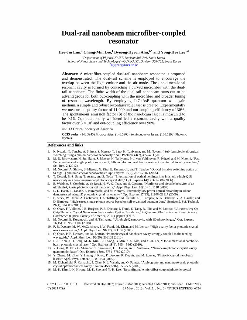
The proposed dual-rail nanobeam structure schematically shown in Fig. 1 is defined by six parameters. Lattice constant (a), thickness (t), radius (r), distance between rails (w) and beam width (b) are 480 nm, 220 nm, 0.35a, 1.2a, 2.7a, respectively. The refractive index of the dielectric material (n) is 3.2 for InGaAsP at room temperature. The dispersion of the dual-rail guided modes is shown in Fig. 1(a). It has three TE-like bands. The two lowest modes are dielectric bands, which are solid curves in Fig. 1(a). The red line shows the dispersion of an air band. A band-gap is present between the 2nd dieletric band and the air band. The dotted and dashed curves represent TM-like modes.
Fig. 1. (a) Dispersion characteristics of a dual-rail structure. a = 480 nm, t = 220 nm, r = 0.35a, w = 1.2a, b = 2.7a as defined in (b). The red solid line is for the air band. The blue and purple solid lines are for the 2nd and 1st dielectric band. (b) The dual-rail structure is defined by lattice constant a, radius of air holes r, spacing between rails w, and beam width b. (c)-(e) Ey field profile (left) and E-field energy density profile (right) of (c) the air band, (d) the 2nd dielectric band and (e) the 1st dielectric band, respectively.
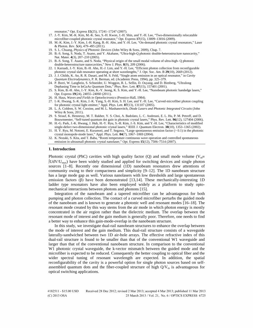
In the presence of a microfiber the effective refractive index of waveguide modes is known to increase. One can expect that evanescent coupling of the dual-rail guided mode with a curved microfiber would create bound modes in the neighborhood of a contact point. Figure 2(a) shows how an air-mode photonic well is formed by touching of a curved microfiber. Two resonant modes are generated in the photonic well that is surrounded by the bandgap.
#182511 - $15.00 USD Received 28 Dec 2012; revised 2 Mar 2013; accepted 4 Mar 2013; published 11 Mar 2013(C) 2013 OSA 25 March 2013 / Vol. 21, No. 6 / OPTICS EXPRESS 6726
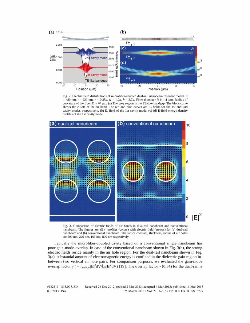
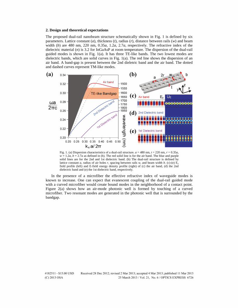
Fig. 2. Electric field distributions of microfiber-coupled dual-rail nanobeam resonant modes. a = 480 nm. t = 220 nm, r = 0.35a. w = 1.2a. b = 2.7a. Fiber diameter D is 1.1 µm. Radius of curvature of the fiber R is 70 µm. (a) The grey region is the TE-like bandgap. The black curve shows the cutoff of the air band. The red and blue curves are Ey fields for the 1st and 2nd cavity modes, respectively. (b) Ey field of the 1st cavity mode, (c)-(d) E-field energy density profiles of the 1st cavity mode.
Fig. 3. Comparison of electric fields of air bands in dual-rail nanobeam and conventional nanobeam. The figures are |(E)|2 profiles (colors) with electric field (arrows) for (a) dual-rail nanobeam and (b) conventional nanobeam. The lattice constant, thickness, radius of air holes are 500 nm, 220 nm, 165 nm, 800 nm respectively.
Typically the microfiber-coupled cavity based on a conventional single nanobeam has poor gain-mode-overlap. In case of the conventional nanobeam shown in Fig. 3(b), the strong electric fields reside mainly in the air hole region. For the dual-rail nanobeam shown in Fig. 3(a), substantial amount of electromagnetic energy is confined in the dielectric gain region in-between two vertical air hole pairs. For comparison purposes, we evaluated the gain-mode overlap factor γ ( = ∫medium|E|2dV/∫all|E|2dV) [19]. The overlap factor γ (0.54) for the dual-rail is
#182511 - $15.00 USD Received 28 Dec 2012; revised 2 Mar 2013; accepted 4 Mar 2013; published 11 Mar 2013(C) 2013 OSA 25 March 2013 / Vol. 21, No. 6 / OPTICS EXPRESS 6727
almost twice as large as that (0.28) of the conventional single nanobeam. Consequently, the dual rail structure is more advantageous for lasing operation.
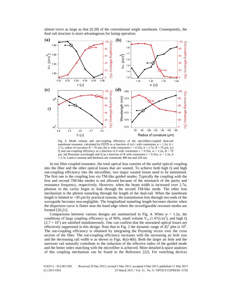
Fig. 4. Mode volume and out-coupling efficiency of the microfiber-coupled dual-rail nanobeam resonator, calculated by FDTD as a function of (a) r with constraints w = 1.2a, b = 2.7a, radius of curvature R = 70 µm, (b) w with constraints r = 0.35a, b = 2.7a, R = 70 µm. (c) Q and out-coupling efficiency as a function of b with constraints r = 0.35a, w = 1.2a, R = 70 µm. (d) Resonant wavelength and Q as a function of R with constraints r = 0.35a, w = 1.2a, b = 2.7a. Lattice constant and thickness are commonly 480 nm and 220 nm.
In our fiber-coupled resonator, the total optical loss consists of the useful optical coupling into the fiber and the other optical losses that are wasted. To achieve both high Q and high out-coupling efficiency into the microfiber, two major wasted losses need to be minimized. The first one is the coupling loss via TM-like guided modes. Typically the coupling with the first and second TM-like modes is not allowed because of the mismatch of the parity and resonance frequency, respectively. However, when the beam width is increased over 2.7a, photons in the cavity begin to leak through the second TM-like mode. The other loss mechanism is the photon tunneling through the length of the dual-rail. When the nanobeam length is limited to ~30 µm by practical reasons, the transmission loss through two ends of the waveguide becomes non-negligible. The longitudinal tunneling length becomes shorter when the dispersion curve is flatter near the band edge where the reconfigurable resonant modes are formed [20,21].
Comparisons between various designs are summarized in Fig. 4. When w = 1.2a, the conditions of large coupling efficiency ηf of 90%, small volume Vm (1.47(λ/n)3), and high Q (2.7 × 10⁷) are satisfied simultaneously. One can confirm that the unwanted optical losses are effectively suppressed in this design. Note that in Fig. 2 the dynamic range of |E|2 plot is 109. The out-coupling efficiency is obtained by integrating the Poynting vector over the cross section of the fiber. The out-coupling efficiency increases with the increasing air hole size and the decreasing rail width w as shown in Figs. 4(a)-4(b). Both the larger air hole and the narrower rail naturally contribute to the reduction of the effective index of the guided mode and the better index matching with the microfiber is achieved. More detailed k-space analyses of this coupling mechanism can be found in the Reference [22]. For switching devices
#182511 - $15.00 USD Received 28 Dec 2012; revised 2 Mar 2013; accepted 4 Mar 2013; published 11 Mar 2013(C) 2013 OSA 25 March 2013 / Vol. 21, No. 6 / OPTICS EXPRESS 6728
employing Kerr nonlinearities, the large Q/Vm is beneficial to obtain the high field intensity with lower incident power [1]. For a single photon source with quantum dot, the large Q/Vm is also advantageous for the high speed operation and the efficient funneling by the enhanced spontaneous emission [2,7]. However, a large Q is not always wanted for both types of devices [1]. The cavity should decay faster than the switching speed (~100 ps) and the de-phasing of QD (~1 ns) [23,24]. Therefore, we believe that a Q of ~105 could be acceptable for both applications.
The tuning characteristics of the reconfigurable mode are studied by varying the radius of curvature R. The 1st cavity mode blue-shifts by a total of 3.7 nm when R changes from 180 to 50 µm as shown in Fig. 4(d). This tuning range is broader than that of the W1 [16,18] photonic crystal waveguide, which can be attributed to the relatively small effective index of the dual-rail nanobeam [17]. In addition, the photonic well of the dual-rail nanobeam is found to be deeper than that of the W1. With increasing radius, the tunneling losses through the two band-gap end mirrors increase. The larger R expands the photonic well and makes the band gap mirror thinner and the out-coupling efficiency is degraded accordingly.
3. Experimental realization
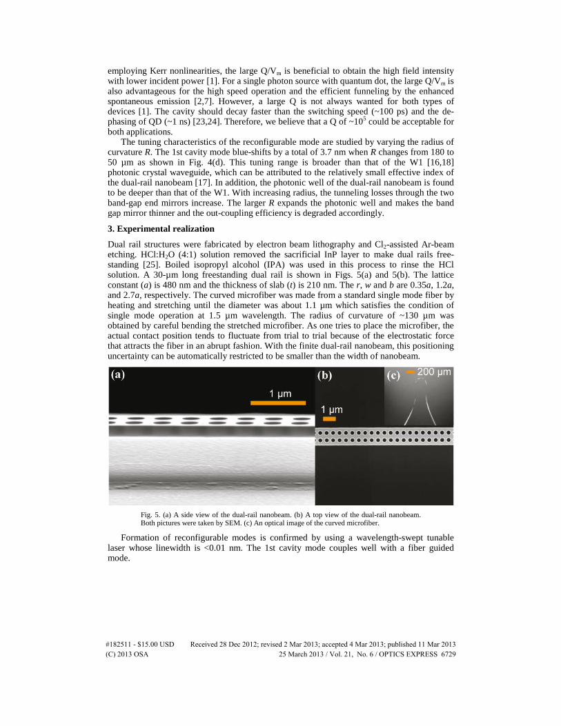
Dual rail structures were fabricated by electron beam lithography and Cl2-assisted Ar-beam etching. HCl:H2O (4:1) solution removed the sacrificial InP layer to make dual rails free-standing [25]. Boiled isopropyl alcohol (IPA) was used in this process to rinse the HCl solution. A 30-µm long freestanding dual rail is shown in Figs. 5(a) and 5(b). The lattice constant (a) is 480 nm and the thickness of slab (t) is 210 nm. The r, w and b are 0.35a, 1.2a, and 2.7a, respectively. The curved microfiber was made from a standard single mode fiber by heating and stretching until the diameter was about 1.1 µm which satisfies the condition of single mode operation at 1.5 µm wavelength. The radius of curvature of ~130 µm was obtained by careful bending the stretched microfiber. As one tries to place the microfiber, the actual contact position tends to fluctuate from trial to trial because of the electrostatic force that attracts the fiber in an abrupt fashion. With the finite dual-rail nanobeam, this positioning uncertainty can be automatically restricted to be smaller than the width of nanobeam.
Fig. 5. (a) A side view of the dual-rail nanobeam. (b) A top view of the dual-rail nanobeam. Both pictures were taken by SEM. (c) An optical image of the curved microfiber.
Formation of reconfigurable modes is confirmed by using a wavelength-swept tunable laser whose linewidth is <0.01 nm. The 1st cavity mode couples well with a fiber guided mode.
#182511 - $15.00 USD Received 28 Dec 2012; revised 2 Mar 2013; accepted 4 Mar 2013; published 11 Mar 2013(C) 2013 OSA 25 March 2013 / Vol. 21, No. 6 / OPTICS EXPRESS 6729
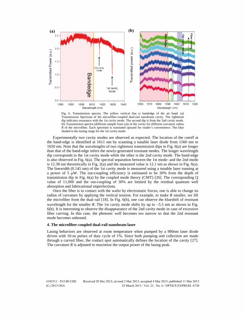
Fig. 6. Transmission spectra. The yellow vertical line is bandedge of the air band. (a) Transmission Spectrum of the microfiber-coupled dual-rail nanobeam cavity. The rightmost dip indicates resonance with the 1st cavity mode. The second dip is from the 2nd cavity mode. (b) Transmission spectra (different sample from (a)) of the cavity for different curvature radius R of the microfiber. Each spectrum is translated upward for reader’s convenience. The blue shaded is the tuning range for the 1st cavity mode.
Experimentally two cavity modes are observed as expected. The location of the cutoff at the band-edge is identified at 1611 nm by scanning a tunable laser diode from 1560 nm to 1650 nm. Note that the wavelengths of two rightmost transmission dips in Fig. 6(a) are longer than that of the band-edge infers the newly-generated resonant modes. The longer wavelength dip corresponds to the 1st cavity mode while the other is the 2nd cavity mode. The band-edge is also observed in Fig. 6(a). The spectral separation between the 1st mode- and the 2nd mode is 12.38 nm theoretically in Fig. 2(a) and the measured value is 12.1 nm as shown in Fig. 6(a). The linewidth (0.145 nm) of the 1st cavity mode is measured using a tunable laser running at a power of 5 µW. The out-coupling efficiency is estimated to be 30% from the depth of transmission dip in Fig. 6(a) by the coupled mode theory (CMT) [26]. The corresponding Q value of 11,000 and the out-coupling of 30% are limited by the residual quantum well absorption and fabricational imperfections.
Once the fiber is in contact with the wafer by electrostatic forces, one is able to change its radius of curvature by applying the vertical tension. For example, to make R smaller, we lift the microfiber from the dual rail [18]. In Fig. 6(b), one can observe the blueshift of resonant wavelength for the smaller R. The 1st cavity mode shifts by up to −5.5 nm as shown in Fig. 6(b). It is interesting to observe the disappearance of the 2nd cavity mode in case of excessive fiber curving. In this case, the photonic well becomes too narrow so that the 2nd resonant mode becomes unbound.
4. The microfiber-coupled dual-rail nanobeam laser
Lasing behaviors are observed at room temperature when pumped by a 980nm laser diode driven with 10-ns pulses of duty cycle of 1%. Since both pumping and collection are made through a curved fiber, the contact spot automatically defines the location of the cavity [27]. The curvature R is adjusted to maximize the output power of the lasing peak.
#182511 - $15.00 USD Received 28 Dec 2012; revised 2 Mar 2013; accepted 4 Mar 2013; published 11 Mar 2013(C) 2013 OSA 25 March 2013 / Vol. 21, No. 6 / OPTICS EXPRESS 6730
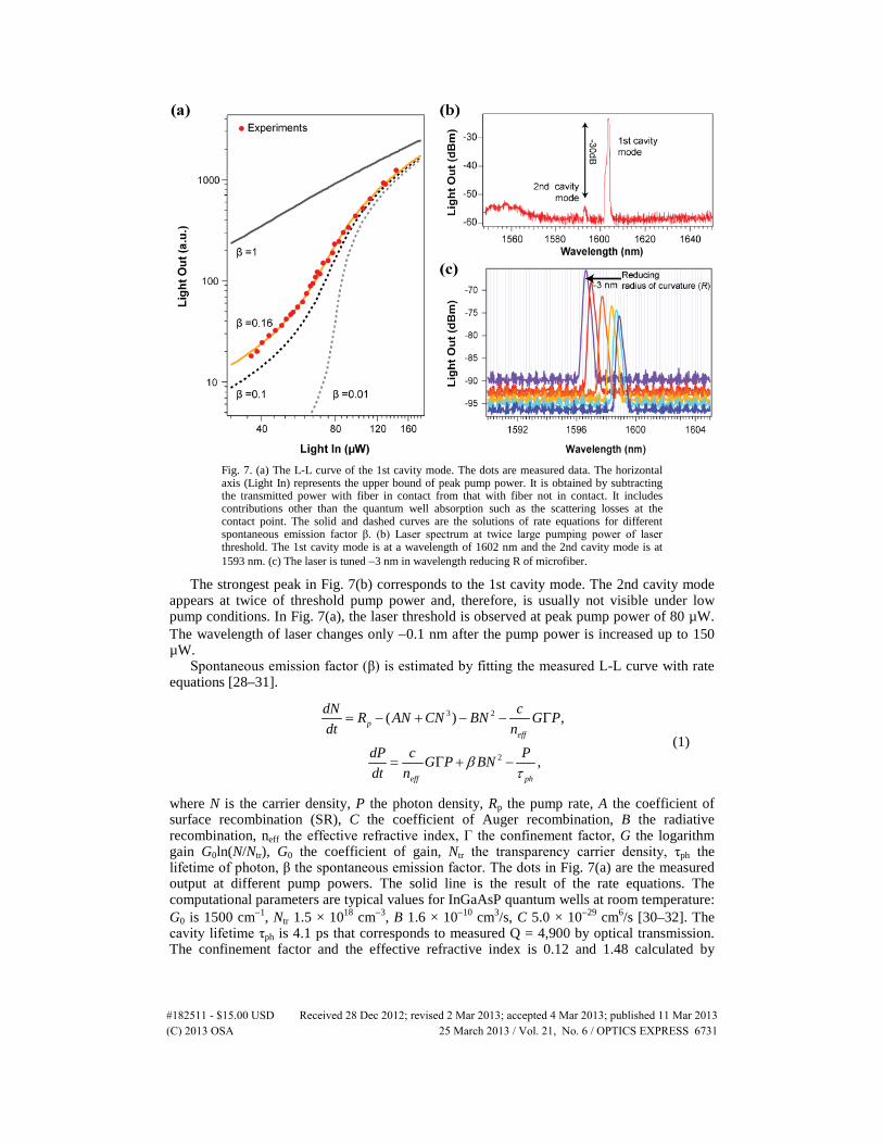
Fig. 7. (a) The L-L curve of the 1st cavity mode. The dots are measured data. The horizontal axis (Light In) represents the upper bound of peak pump power. It is obtained by subtracting the transmitted power with fiber in contact from that with fiber not in contact. It includes contributions other than the quantum well absorption such as the scattering losses at the contact point. The solid and dashed curves are the solutions of rate equations for different spontaneous emission factor β. (b) Laser spectrum at twice large pumping power of laser threshold. The 1st cavity mode is at a wavelength of 1602 nm and the 2nd cavity mode is at 1593 nm. (c) The laser is tuned −3 nm in wavelength reducing R of microfiber.
The strongest peak in Fig. 7(b) corresponds to the 1st cavity mode. The 2nd cavity mode appears at twice of threshold pump power and, therefore, is usually not visible under low pump conditions. In Fig. 7(a), the laser threshold is observed at peak pump power of 80 µW. The wavelength of laser changes only −0.1 nm after the pump power is increased up to 150 µW.
Spontaneous emission factor (β) is estimated by fitting the measured L-L curve with rate equations [28–31].
3 2
2
( ) ,
,
peff
eff ph
dN cR AN CN BN G Pdt n
dP c PG P BNdt n
βτ
= − + − − Γ
= Γ + − (1)
where N is the carrier density, P the photon density, Rp the pump rate, A the coefficient of surface recombination (SR), C the coefficient of Auger recombination, B the radiative recombination, neff the effective refractive index, Γ the confinement factor, G the logarithm gain G0ln(N/Ntr), G0 the coefficient of gain, Ntr the transparency carrier density, τph the lifetime of photon, β the spontaneous emission factor. The dots in Fig. 7(a) are the measured output at different pump powers. The solid line is the result of the rate equations. The computational parameters are typical values for InGaAsP quantum wells at room temperature: G0 is 1500 cm−1, Ntr 1.5 × 1018 cm−3, B 1.6 × 10⁻¹⁰ cm3/s, C 5.0 × 10⁻²⁹ cm6/s [30–32]. The cavity lifetime τph is 4.1 ps that corresponds to measured Q = 4,900 by optical transmission. The confinement factor and the effective refractive index is 0.12 and 1.48 calculated by
#182511 - $15.00 USD Received 28 Dec 2012; revised 2 Mar 2013; accepted 4 Mar 2013; published 11 Mar 2013(C) 2013 OSA 25 March 2013 / Vol. 21, No. 6 / OPTICS EXPRESS 6731
FDTD calculations. In the rate equation the surface recombination term is neglected. This approximation results in the lower bound of the spontaneous emission factor β = 0.16.
By reducing the radius of curvature of the microfiber, we are able to tune resonant wavelength by −3 nm as shown in Fig. 7(c). The observed tuning range maintaining uniform laser action is smaller than that of transmission measurements in Fig. 6(b) because the curvature change affects both the Q value and the coupling efficiency [18] as expected in Fig. 4(d).
5. Conclusion
We propose and demonstrate microfiber-coupled dual-rail nanobeam resonators that can be tuned up to 5.5 nm in wavelength. The fiber-coupled resonant cavity shows out-coupling efficiency of 30% and Q of 11,000 by transmission measurements. When operated as a reconfigurable microlaser, the spontaneous emission factor (β) of >0.16 is estimated from the rate equation analysis. The proposed microfiber-coupled dual-rail nanobeam resonator could be a promising candidate for an efficient single photon source. The high Q/V value of this configuration could also be advantageous for power-sensitive nonlinear devices.
Acknowledgment
H.-J. Lim would like to thank Dr. Ho-Seok Ee in Nano laser laboratory at Korea University and his FDTD tool named “ALiS”. B.-H. Ahn is supported by National Junior Research Fellowship which National Research Foundation of Korea conducts from 2010. This work was supported by the National Research Foundation of Korea (NRF) grant funded by the Korea government (MEST) (No. 2007-0093863, 2009-0087691, 2012-00087, R31-2008-000-10071-0).
#182511 - $15.00 USD Received 28 Dec 2012; revised 2 Mar 2013; accepted 4 Mar 2013; published 11 Mar 2013(C) 2013 OSA 25 March 2013 / Vol. 21, No. 6 / OPTICS EXPRESS 6732