a dna biosensor based interface states of a metal...
TRANSCRIPT
Vol. 121 (2012) ACTA PHYSICA POLONICA A No. 3
A DNA Biosensor Based Interface Statesof a Metal�Insulator�Semiconductor Diode
for Biotechnology ApplicationsA.A. Al-Ghamdia, O.A. Al-Hartomya,b, R. Guptac, F. El-Tantawyd, E. Taskane,
H. Hasare and F. Yakuphanogluf,∗
aDepartment of Physics, Faculty of Science, King Abdulaziz University, Jeddah, Saudi ArabiabDepartment of Physics, Faculty of Science, Tabuk University, Tabuk 71491, Saudi Arabia
cEngineering Research Center, North Carolina A & T State University, Greensboro, North Carolina 27411, USAdDepartment of Physics, Faculty of Science, Suez Canal University, Ismailia, Egypt
eDepartment of Environmental Engineering, Firat University, Elazi§, Turkey
Center for Biotechnology Research, Firat University, Elazig, TurkeyfDepartment of Physics, Faculty of Science, Firat University, Elazig, Turkey
(Received June 21, 2011; revised version December 2011; in �nal form January 2, 2012)
We studied how a DNA sensor based on the interface states of a conventional metal�insulator�semiconductordiode can be prepared for biotechnology applications. For this purpose, the p-type silicon/metal diodes wereprepared using SiO2 and DNA layers. The obtained results were analyzed and compared with interfaces of DNAand SiO2. It is seen that the ideality factor (1.82) of the Al/p-Si/SiO2/DNA/Ag diode is lower than that (3.31) ofthe Al/p-Si/SiO2/Ag diode. This indicates that the electronic performance of DNA/Si junction was better thanthat of SiO2/Si junction. The interface states of the Al/p-Si/SiO2/DNA/Ag and Al/p-Si/SiO2/Ag junctions wereanalyzed by conductance technique. The obtained Dit values indicate that the DNA layer is an e�ective parameterto control the interface states of the conventional Si based on metal/semiconductor contacts. Results exhibitedthat DNA based metal�insulator�semiconductor diode could be used as DNA sensor for biotechnology applications.
PACS: 73.40.Jn, 81.05.Fb, 73.30.+y
1. Introduction
The metal/semiconductor (MS) contacts are of greatimportance for the potential use in electronic and opto-electronic devices [1�4] and MS diodes have been studiedby many researchers using various organic semiconduct-ing materials [5�8]. It is well known that the electri-cal characteristics of metal/semiconductor contacts arecontrolled mainly by their surface properties [8�11]. AnMS diode possesses a thin interfacial native oxide layer,which has a big in�uence on electrical characteristics ofdiode [10]. The electrical properties of MS diode can becontrolled by adsorption of small organic compound onthe inorganic semiconductor surface. The deoxyribonu-cleic acid (DNA), which is central to every living organ-ism, is a subject of interest for its physical properties,and particularly for a great potential of application inphotonics and molecular electronics [12]. DNA can besynthesized arti�cially and extracted from living organ-isms in its purity. It is the most stable molecule evenunder high temperature conditions (90 ◦C) [13].DNA device with metal/semiconductor contacts are
still rare [14�16]. In recent years, there are some stud-ies on the electrical conduction of the DNA moleculeswhich reveal that they may act as either semiconductorwith nanosize dimensions or non-semiconductor materi-als (i.e., insulator or metal) [17�19].
∗ corresponding author; e-mail: [email protected]
In our previous study, we have fabricated a Al/p-Si/DNA/Ag diode for optical sensor applications, in whichwe have used DNA of band 15 at all microbial fuel cell(MFC) samples detected as Shewanella halitotis [20].In present study, we have used DNA of band 18 at all
microbial fuel cell (MFC) samples detected as Entero-coccus sp. and SiO2 layer to fabricate a Al/p-Si/SiO2/DNA/Ag diode. To best of our knowledge, no study onAl/p-Si/SiO2/DNA/Ag diode has been reported. Theaim of this study is to fabricate a DNA based MS diodefor electronic device applications. DNA puri�ed from anMFC operating in the environmental biotechnology areawas used to develop the biosensor. The current�voltageand capacitance�voltage measurements were performedto analyze the electrical properties of the DNA basedMS diode.
2. Experimental details
2.1. DNA protocol description
Total DNA was extracted from the MFC, whichproduces directly the electricity energy while treatingwastewater, at di�erent time intervals to reveal thechanges in the microbial communities over time usingdenaturing gradient gel electrophoresis (DGGE) analy-sis. DNA was extracted with PowerSoil DNA isolationkit according to manufacturer's instructions. ExtractedDNA samples were stored at −20 ◦C. The crude DNAsample including a mixed culture was used as a template
(673)
674 F. Yakuphanoglu et al.
for the polymerase chain reaction (PCR). Fragments cor-responding to nucleotide positions 341�534 of the Es-cherichia coli 16S rRNA gene sequence were ampli�edwith the forward primer GC-BacV3f (5-CCT ACG GGAGGC AGC AG-3) to which at the 5′ end a GC clampwas added to stabilize the melting behavior of the DNAfragments in the DGGE, and the reverse primer 534r (5′
� ATT ACC GCG GCT GCT GG-3′) [21]. PCR ampli-�cation was performed using Thermocycler TECHNE/TC-512 with the following program: initial denaturationat 95 ◦C for 5 min followed by 30 cycles of denaturationat 94 ◦C for 30 s, primer annealing at 50 ◦C for 1 min andprimer extension at 72 ◦C for 2 min, and �nal extensionat 72 ◦C for 10 min.The presence of PCR products was con�rmed by
1% (w/v) agarose gel electrophoresis and staining withethidium bromide prior to DGGE analysis. DGGE wasperformed with the INGENY phor U-2, Ingeny Interna-tional BV. PCR samples were loaded onto 8% (w/v) poly-acrylamide gel (acrylamide/bisacrylamide (37.5:1) stocksolution, Bio�Rad) in TAE (40 mM Tris, 20 mM aceticacid, 1 mM EDTA, pH 8.3) with denaturing gradientranging from 35% to 60% (100% denaturant contains 7 Murea and 40% formamide). The electrophoresis was runat 60 ◦C with 100 V for 18 h.
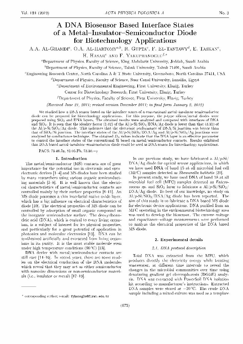
Fig. 1. (a) DGGE bands for �ve MFC conditions, (b)AFM image of the DNA thin �lm deposited on theSiO2/Si.
After electrophoresis, the gel was stained in a SYBRgold solution (100 mL/L in TAE) for 35 min and pho-tographed by a Gel Monitoring System (Vilberlourmat),as seen in Fig. 1a. Bands in DGGE gels were excised witha razor blade and placed in sterile 1 ml vials. DNA waseluted into 20 mL of water and frozen at −20 ◦C. Theeluted DNA was used as template in PCR reactions withthe primers BacV3f (without GC clamp) and 534r usingthe same PCR programs described above. The sequenc-ing of the puri�ed products was performed at DNA Se-quencing Facility, IONTEK �rm, Turkey. DGGE of 16SrRNA genes was applied to reveal successive changes inthe microbial communities of the MFC (Fig. 1a). In theDGGE analysis, 18 bands were numbered at di�erent op-erating conditions. Band 18 at all MFC samples was de-tected as Enterococcus sp. (Accession No. AY489118.1),which means dominant microorganism in MFC.
2.2. Fabrication of the diodes
For fabrication of the p-Si/SiO2 [20] and p-Si/SiO2/DNA diodes, a p-Si wafer was �rstly chemically cleanedusing the RCA cleaning procedure. After surface clean-ing, the Al metal was evaporated onto p-Si substrateusing a PVD-HANDY/2S-TE (Vaksis Company) vac-uum thermal evaporation. The native oxide on p-Silayer was removed in HF+10H2O solution and then wasrinsed in deionized water using an ultrasonic bath for10�15 min and �nally was chemically cleaned accordingto method based on successive baths of methanol andacetone. The Si substrates were used for the prepara-tion of the diodes. One of them was oxidized at roomtemperature for 2 days. Then, the DNA �lm was care-fully placed by deposition of 10 µ L DNA solution on thep-Si wafer by spin coating technique and slowly spreadon top of it and then, it was dried at room tempera-ture for 12 h. The thickness of the DNA �lm was ob-tained to be 360 ± 2.5 nm. The Schottky contact wasformed by Ag paint on the DNA organic layer. The pre-pared diodes are Al/p-Si/SiO2/DNA/Ag and Al/p-Si/SiO2/Ag [20] junctions. The diode contact area wascalculated to be 3.14 × 10⁻² cm2. The current�voltage(I�V ) and capacitance�voltage (C�V ) characteristics ofthe Al/p-Si/SiO2/DNA/Ag and Al/p-Si/SiO2/Ag junc-tions were measured with Keithley 4200 semiconductorcharacterization system.
3. Results and discussion
3.1. Structural properties and electrical characteristics
The AFM image of the DNA thin �lm deposited on theSiO2/Si is shown in Fig. 1b. As seen in Fig. 1b, the DNAmolecules are formed from the clusters. The roughnessof the �lm was determined to be 26.9 nm.In our previous study, we have fabricated an
Al/p-Si/Ag junction and we have analyzed its electri-cal characterization by I�V and C�V measurements [20].The obtained results indicated that the ideality factorof the Al/p-Si/Ag diode is higher than unity. Thus,in present study, we evaluated that Al/p-Si/Ag diodehas a metal�oxide�semiconductor structure as Al/p-Si/SiO2/Ag. The electrical characteristics of Al/p-Si/Agdiode (hereinafter �Al/p-Si/SiO2/Ag diode�) were usedto explain the e�ect of Enterococcus sp. DNA layer onthe electrical parameters of the Al/p-Si/Ag diode.The current�voltage characteristics of the Al/p-Si/
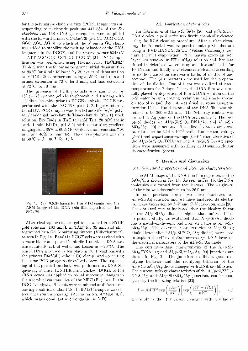
SiO2/DNA/Ag and Al/p-Si/SiO2/Ag [20] junctions areshown in Fig. 2. The junctions exhibit a good rec-tifying behavior and the rectifying behavior of theAl/p-Si/SiO2/Ag diode changes with DNA modi�cation.The current�voltage characteristics of the Al/p-Si/SiO2/DNA/Ag and Al/p-Si/SiO2/Ag junctions can be ana-lyzed by the following relation [22]:
I = AA∗T 2 exp
(qϕeff
kT
)[exp
(q(V − IRs)
nkT
)], (1)
where A∗ is the Richardson constant with a value of
A DNA Biosensor Based Interface States . . . 675
Fig. 2. Current�voltage characteristics of the Al/p-Si/SiO2/DNA/Ag and Al/p-Si/SiO2/Ag [20] junctions.
32 A cm−2K−2 for p-type silicon, Rs is the series resis-tance, V is the applied voltage, n is the ideality factor,k is the Boltzmann constant, T is the temperature andϕeff is the e�ective barrier given by [23, 24]:
qϕeff = qϕb + kTβl, (2)
where β is the structure-dependent attenuation factorthat depends on the tunneling mechanism, l is the �lmthickness of DNA �lm and the second term in Eq. (2)contributes to the e�ective barrier height of the interfa-cial layer.
As seen in Fig. 2, the I�V characteristics of the diodeare linear at lower forward voltages. The ideality fac-tors of the Al/p-Si/SiO2/DNA/Ag and Al/p-Si/SiO2/Agjunctions were obtained to be 1.82 ± 0.15 and 3.31 ±0.11, respectively. The ideality factor of the Al/p-Si/SiO2/DNA/Ag diode is lower than that of the Al/p-Si/SiO2/Ag. This indicates that the electronic performanceof DNA/Si junction is changed by DNA molecules. Thebarrier height values of the Al/p-Si/SiO2/DNA/Ag andAl/p-Si/SiO2/Ag diodes were obtained to be 0.76 eV and0.82 eV, respectively, and these values are higher thanthat of Ag/p-Si, Al/SiO2/p-Si Schottky barrier diodes,Al/tetraamide-I/p-Si diode, Ag/Zn(Phen)q/p-Si diode,Ag/FSS/p-Si diode [25�29]. The obtained barrier height(0.76 eV) of the Al/p-Si/SiO2/DNA/Ag is lower thanthat of Al/p-Si/SiO2/Ag diode (0.82 eV), whereas it ishigher than that of p-Si/DNA diode (0.56 eV) [20]. Thissuggests that the DNA organic layer modi�es the bar-rier height and DNA layer gives an excess barrier. Thestudies in literature have shown that e�ective Schottkybarrier could be either increased or decreased by usingorganic thin layer on inorganic semiconductor [30�34].
The decrease in the barrier height can result fromthe realignments between the lowest unoccupied molec-ular orbital (LUMO), highest occupied molecular orbital(HOMO) of the DNA layer and work function of themetal. The surface modi�cation of DNA layer leads to
the changes in the electronic properties of the metal�semiconductor devices due to the molecular tunability ofmetal/semiconductor diodes.
3.2. Interface state density properties
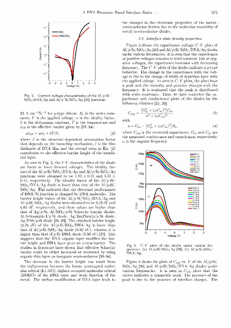
Figure 3 shows the capacitance�voltage C�V plots ofAl/p-Si/SiO2/Ag [20] and Al/p-Si/SiO2/DNA/Ag diodesunder various frequencies. It is seen that the capacitanceat positive voltages remains to tend constant, but at neg-ative voltages, the capacitance increases with decreasingfrequency. The C�V plots of the diodes indicate a p-typebehavior. The change in the capacitance with the volt-age is due to the change of width of depletion layer withthe applied voltage. As seen in C�V plots, the plots havea peak and the intensity and position changes with thefrequency. It is evaluated that the peak is distributedwith series resistance. Thus, we have corrected the ca-pacitance and conductance plots of the diodes by thefollowing relations [35, 36]:
Cadj =
[G2
m + (ωCm)2]Cm
a2 + (ωCm)2(3)
with
a = Gm −[G2
m + (ωCm)2]Rs, (4)
where Cadj is the corrected capacitance, Gm and Cm arethe measured conductance and capacitance, respectively,ω is the angular frequency.
Fig. 3. C�V plots of the diodes under various fre-quencies: (a) Al/p-Si/SiO2/Ag [20], (b) Al/p-Si/SiO2/DNA/Ag.
Figure 4 shows the plots of Cadj vs. V of the Al/p-Si/SiO2/Ag [20] and Al/p-Si/SiO2/DNA/Ag diodes undervarious frequencies. It is seen in Cadj plots that thecurves indicates a symmetric peak. The presence of thepeak is due to the presence of interface charges. The
676 F. Yakuphanoglu et al.
Fig. 4. Cadj�V plots of the diodes under various fre-quencies: (a) Al/p-Si/SiO2/Ag [20], (b) Al/p-Si/SiO2/DNA/Ag.
Fig. 5. Plots of Cadj�V of the diodes under various fre-quencies: (a) Al/p-Si/SiO2/Ag [20], (b) Al/p-Si/SiO2/DNA/Ag.
peak intensity decreases with increasing frequency. Theconductance�voltage plots of the diodes were correctedby the following relation [35, 36]:
Gadj =
[G2
m + (ωCm)2]a
a2 + (ωCm)2, (5)
where Gadj is the corrected conductance.
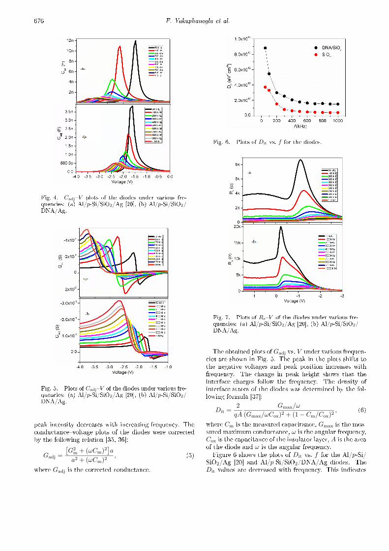
Fig. 6. Plots of Dit vs. f for the diodes.
Fig. 7. Plots of Rs�V of the diodes under various fre-quencies: (a) Al/p-Si/SiO2/Ag [20], (b) Al/p-Si/SiO2/DNA/Ag.
The obtained plots ofGadj vs. V under various frequen-cies are shown in Fig. 5. The peak in the plots shifts tothe negative voltages and peak position increases withfrequency. The change in peak height shows that theinterface charges follow the frequency. The density ofinterface states of the diodes was determined by the fol-lowing formula [37]:
Dit =2
qA
Gmax/ω
(Gmax/ωCox)2 + (1− Cm/Cox)2, (6)
where Cm is the measured capacitance, Gmax is the mea-sured maximum conductance, ω is the angular frequency,Cox is the capacitance of the insulator layer, A is the areaof the diode and ω is the angular frequency.Figure 6 shows the plots of Dit vs. f for the Al/p-Si/
SiO2/Ag [20] and Al/p-Si/SiO2/DNA/Ag diodes. TheDit values are decreased with frequency. This indicates

A DNA Biosensor Based Interface States . . . 677
that the interface charges follow the frequency of appliedvoltage. The width of peak in the Cadj�V curves withfrequency is related to the number of trapped carriercharges at interface. The Dit values of the Al/p-Si/SiO2/DNA/Ag are higher than that of Al/p-Si/SiO2/Ag junc-tion [20]. This indicates that the DNA layer changes theinterface states of Al/p-Si/SiO2/Ag junction.The series resistance plots of the diodes are shown in
Fig. 7. As seen in Fig. 7, the series resistance changeswith frequency and indicates a peak. The intensity andposition of the peak change with the frequency. The in-tensity of the peak decreases and disappears. The peakintensity for Al/p-Si/SiO2/DNA/Ag diode is higher thanthat of Al/p-Si/SiO2/Ag junction. This indicates thatAl/p-Si/SiO2/DNA/Ag diode has the higher Dit valuesthan Al/p-Si/SiO2/Ag junction.
4. Conclusions
We have fabricated Al/p-Si/SiO2/DNA/Ag andAl/p-Si/SiO2/Ag junctions. The electrical performancesof the diodes were determined by I�V and G�C�Vmeasurements. The junctions exhibit a good rectify-ing behavior and the rectifying behavior of the Al/p-Si/SiO2/Ag diode changes with DNA modi�cation. Thediodes indicate a metal�insulator�semiconductor struc-ture. It was found that the Dit values of the Al/p-Si/SiO2/DNA/Ag are higher than that of Al/p-Si/SiO2/Agjunction. This indicates that the DNA layer increasesthe interface states of the conventional Si based on MScontacts.
Acknowledgments
The present study is a result of an international col-laboration program between University of Tabuk, Tabuk,Saudi Arabia and Firat University, Elazig, Turkey. Theauthors gratefully acknowledge the �nancial supportfrom the University of Tabuk, project no. 4/1433.
References
[1] T. Maeda, S. Takagi, T. Ohnishi, M. Lippmaa,Mater.Sci. Semicond. Process. 9, 706 (2006).
[2] M. Shah, M.H. Sayyad, Kh.S. Karimov, M.M. Tahir,Physica B 405, 1188 (2010).
[3] M. Shah, M.H. Sayyad, Kh.S. Karimov, M.M. Tahir,Optoelectr. Adv. Mater. � Rapid Comm. (OAM-RC) 3, 831 (2009).
[4] F. Yakuphanoglu, Synth. Met. 158, 108 (2008).
[5] S. Aydogan, Ü. Incekara, A.R. Deniz, A. Türüt, Mi-croelectron. Eng. 87, 2525i (2010).
[6] J.S. Park, B.R. Lee, J.M. Lee, J.S. Kim, S.O. Kim,M.H. Song, Appl. Phys. Lett. 96, 243306 (2010).
[7] S. Aydogan, K. Çinar, H. Asil, C. Coskun, A. Türüt,J. Alloys Comp. 476, 913 (2009).
[8] P. Hanselaer, W.H. La�ére, R.L. Van Meirhaeghe,F. Cardon, Appl. Phys. A 39, 129 (1986).
[9] R.L. Van Meirhaeghe, W.H. La�ére, F. Cardon,J. Appl. Phys. 76, 403 (1994).
[10] P. Hanselaer, W.H. La�ére, R.L. Van Meirhaeghe,F. Cardon, Appl. Phys. 56, 2309 (1984).
[11] �. Aydo§an, M. Sa§lam, A. Türüt, Vacuum 77, 269(2005).
[12] V. Kazukauskas, M. Pranaitis, A. Arlauskas,O. Krupka, F. Kajzar, Z. Essaidi, B. Sahraoui, Opt.Mater. 32, 1629 (2010).
[13] R.K. Gupta, V. Saraf, Curr. Appl. Phys. 9, S149(2009).
[14] S. Okur, F. Yakuphanoglu, M. Ozsoz, P. Kara Ka-dayifcilar, Microelectron. Eng. 86, 2305 (2009).
[15] O. Gullu, A. Turut, J. Alloys Comp. 509, 571 (2011).
[16] O. Gullu, Microelectron. Eng. 87, 648 (2010).
[17] L. Cai, H. Tabata, T. Kawai, Appl. Phys. Lett. 77,3105 (2000).
[18] A.Y. Kasumov, M. Kociak, S. Gueron, B. Reulet,V.T. Volkov, D.V. Klinov, H. Bouchiat, Science 291,280 (2001).
[19] A.J. Storm, J. Van Noort, S. de Vries, C. Dekker,Appl. Phys. Lett. 79, 3881 (2001).
[20] R.K. Gupta, F. Yakuphanoglu, H. Hasar, A.A. al--Khedhairy, Synthetic Met. 161, 2011 (2011).
[21] G. Muyzer, E. De Waal, A.G. Uitterlinden, Appl. En-vironmen. Microbiol. 59, 695 (1993).
[22] E.H. Rhoderick, Metal�Semiconductor Contacts, Ox-ford University Press, Oxford 1978.
[23] Y. Selzer, A. Salomon, D. Cahen, J. Phys. Chem. B106, 10432 (2002).
[24] Y.J. Liu, H.Z. Yu, Chem. Phys. Chem. 3, 799 (2002).
[25] S. Acar, S. Karadeniz, N. Tu§luo§lu, A.B. Selçuk,M. Kasap, Appl. Surf. Sci. 233, 373 (2004).
[26] A. Tataro§lu, �. Alt�ndal, M.M. Bülbül, Nucl. In-strum. Methods Phys. Res. A 568, 863 (2006).
[27] T. K�l�coglu, M.E. Ayd�n, G. Topal, M.A. Ebeoglu,H. Sayg�l�, Synthetic Met. 157, 540 (2007).
[28] F. Yakuphanoglu, B.J. Lee, Physica B 390, 151(2007).
[29] M.E. Aydina, F. Yakuphanoglu, J. Phys. Chem.Solids 68, 1770 (2007).
[30] F. Yakuphanoglu, B.-J. Lee, Physica B 390, 151(2007).
[31] M.E. Aydin, F. Yakuphanoglu, Jae-Hoon Eom, Do--Hoon Hwang, Physica B 387, 306 (2007).
[32] M. Çakar, N. Y�ld�r�m, H. Do§an, A. Türüt, Appl.Surf. Sci. 252, 2209 (2006).
[33] �. Aydo§an, M. Sa§lam, A. Türüt, Polymer 46, 10982(2005).
[34] I.H. Campbell, S. Rubin, T.A. Zawodzinski,J.D. Kress, R.L. Martin, D.L. Smith, N.N. Barashkov,J.P. Ferraris, Phys. Rev. B 54, 14321 (1996).
[35] E.H. Nicollian, A. Goetzberger, Bell Syst. Technol. J.46, 1055 (1967).
[36] I. Dökme, �. Alt�ndal, T. Tunç, I. Uslu,Microelectron.Reliab. 50, 39 (2010).
[37] W.A. Hill, C.C. Coleman, Solid State Electron. 23,987 (1980).