a dsp-56001 software architecture for a radio and data...
TRANSCRIPT

National LiSrary of Canada
Bibliothttque nationate du Canada
Acquisitions and Direction des acquisitions et Bibliographic Services Branch des services bibtiographiques
395 Wellington Streer 395, rue Wellington Ottawa, Ontario Oflawa {Ontarioj K IA OIJ4 K I P ON4
?',?u< !t~e VGIW -&r'?r,?*
The quality of this heavily depen ent upon the t de la qualit6 quality of the originat thesis de !a thQse sou aea submitted Bsr microfilmin ous avons taut Every effort has been made to fait pour assures ensure the highest quality sf superieure de reproduction. reproduction possible.
If pages are missing, contact the anque ties pages, veuillem university which granted the uer avec I9universit& degree. qui a conf6r6 le grade.
Some pages may have indistinct La qualit@ d'impression de print especially if the original certaines pages peut laisser 6 pages were typed with a poor dhirer, surtout si les pages typewriter ribbon or if the originales ont @t tSf university sent us an inferior dactylographibes b i d e d'un photocopy. ruban us6 ou si 'I'universite nsus
a fait parvenir une phatoc~pie de qualit6 infbrieure.
Reproduction in dull or in part sf La reproduction, mgme partielk, this microform is governed by de cette microforme est sostrrrise the Canadian Copyright Act, a ta boi canadienne sur le droit R.S.C. 3970, c. C-30, and d'auteur, SRC 1970, c. C-30: et subsequent amendments. ses amendements subsequents.
A ESP-56001 SCET%'XRE ARCHITECTURE FOR A
RADIO AS3 DATA PACKET CONTROLLER
B.A.Sc., Tv'niversit;~ of British Columbia, 1984
PROJECT SUBMITTED I?;- PARTIAL FULFILLMENT OF
TFIE REQUIKEhlDElXSTS FOR THE DEGREE OF
MASTER OF EWGZPEERING
ZV THE SCHOOL OF ENGTNEERING SCIENCE
G LYillIam Chez-Foon Chong
SIhlON FRASER UNIVERSITY
Ail rights ressrved. This work may not be
reproduced in whole or in part, by photocopy or
other means, without permission of the author

BibIiolheque natiijnafe dit Canada
Acquisitions and Direction des acquisitions et Bibtiographic Servkes Branch des services Sibiiagraphiques
The author has granted an irrevocable non-exclusive licence allowing the National Library af Canada to reproduce, ioan, distribute or sell copies of his/her thesis by any means and in any form or dormat, making this thesis available to interested persons.
L'auteur a accord6 sne licence iaa6arocabte et now exclh~sive
ermeffanf 6 9a nationale du Canada de reproduire, prkter, distribuer ou
re des copies de sa these de quelque manigre et sous quelque forme que ce soit pour mettre des etcernphires be cette these B la disposition des personnes int6ress6es.
The author retains ownership of L'auteur conserve la proprietb du the copyright in his/her thesis. droit d'auteur qui protege sa Neither the thesis nor substantial these. Ni ta thhse nS des extraits extracts from it may be printed or substantieis de ceiie-ei ne otherwise reproduced without doivent &re imprimes ou his/her permission. autrernent reprodhiits sans son
autorisatisn.
DEGREE: Master of Engineering
TITLE OF PROJEC~'T: A DSP-56001 Software Architecture fur a Radio and Data Packet Controller
Dr. Shawn Stapleton Assistant Professor
Dr. Jacques Vaisey Assistant Professor
Mr. Peter McConneU External Examiner
DATE APPROVED: December 1 1, 199 1

PARTIAL COPYRIGHT LICENSE
I hereby grant to Simon Fraser University the right to tend
my thesis, project or extended essay (the title of which i s shown below)
to users of the Simon Fraser University Library, and to make partial or
single copies only for such users or in response to a request from the
library of any other university, or other educationai institution, on
its own behalf or for one of i t s users. I further agree that permission
for multiple copying of this work for scholarly purposes may be granted
by me or the Dean of Graduate Studies. It is understood that copying
or publication o f this work for financial gain snali not be allowed
without my written permission.
T i t l e of Thesis/Project/Extended Essay
- A DSP-56001 Software A r c h i t e c t u r e f o r a Radio an2
Data Packet Con t ro l l e r
Author:
Is i gnature)
12 D e c e m b e r 1 9 9 1
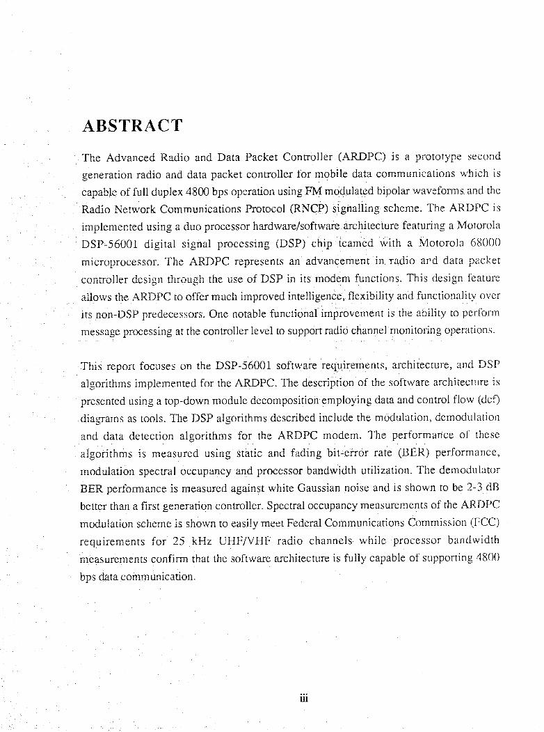
ABSTRACT
The Advanced Radio and Data Packet Controller (ARDPC) is a prototype second
generation radio and data packet controller for mobile data communications which is U
capable of full duplex 4800 bps operation using FM modulated bipolar waveforms and the
Radio Network Communications Protocol (RNCP) signalling scheme. The ARDPC is
impfemsnted using a duo processor hardware/software architecture featuring a Motorola
DSP-56001 digital signal processing (DSP) chip teamed with a Motorola 68000
microprocessor. The ARDPC represents an advancement in radio a d data packet
corn-ofler design through the use of DSP in its modem functions. This design feature
alotvs the ARDPC to offer much improved intelligence, flexibility and functionality over
its non-DSP predecessors, One notable functional improvement is the ability to perform
message processing at the controller level to support radio channel monitoring operations.
This report focuses on the DSP-56001 software requirements, architecture, and DSP
algorithms implemented for the ARDPC. The description of the software architecture is
presented using a top-down module decomposition employing data and control flow (dcf)
diagrans as took. The DSP algorithms described include the modulation, demodulation
and data detection algorithms for ths ARDPC modem. The performance of these
algorithms is measured using static and fading bit-error rate (BER) performance,
modulation spect~al occupancy and processor bandwidth utilization. The demodulator
BER performance is measured against white Gaussian noise and is shown to be 2-3 dB
better than a first generation controller. Spectral occupancy measurements of the ARDPC
modulation scheme Is shown to easily meet Federal Communications Commission (FCC)
requirements for 25 kHz UHF/VHF radio channels while processor bandwidth
measurements confirm that the software architecture is fully capable of supponing 4800
bps data communication.

TABLE of CONTENTS
............................................................................................... Approvd ii ... ............................................................................................... Abstract 111
.................................................................................... Table of Contents iv ... ..................................................................................... List of Tables WI
....................................................................................... List of Figures ix
.............................................................. List of Acronyms and Abbreviations xi
SECTION I: INTRODUCTION 2.1 Project Background ................................................................ 1
3 ................................................................ 1.2 Document Overview - SECTION 2: RNCP NETWORK OVERVIEW
2.1 Physical Link Descriphon ......................................................... 3
.................................................... 2.1.1 Mobile Data Terminals 6
............................................................. 2.1.2 Host Computer 6
2.1.3 Communications Controller .............................................. 6
2.1 -3 Radio and Data Packet Controller ........................................ 7
2.1.5 Channel Multiplexer ....................................................... 7
2.2 Data Link Description
...................................................... 2.2.1 Bit Level Description 8
2.2.2 Packet Structure ............................................................ 9
2.2.2.1 Message Symbols ............................................ 9
............................................ 2.2.2.2 Message Header 11
2.2.2.3 MessageTextBlocks ...................................... 11
2.2.2.4 Message Preamble ......................................... 13
2.2.2.5 Channel Contention Control .............................. 13
2.2.2.6 Network Synchronization ................................. 13
SECTION 3: ARD'PC OVERVIEW ........................................................ 3. 1 Functional Requirements 15
....................................................... 3.1.1 Modem Functions 16
..................................................... 3.1 -2 CC Communication 16
................................................ 3.1.3 Base Sire Radio Control 16
3.1.4 Radio Channel Access Control ........................................ 16
3.1 . 5 VMEbus capability ...................................................... 17
3.1.6 User Console Interface ....................... 0 1 7 Improved Diagnostics ............................
iv

.............................. 3.1.8 Lesel Adjustments from Local Console 17 ............................................ 3.1.9 E C Decoding of Messages 18
........................................... 3 . I . f Q Radio Channel Monitoring.. 18
........................................... 3.1.1 1 RNCP Message Monitoring 18
............................ 3-1-22 RF Alarms and RSSI Signal Monitoing i 8 ............................................................ 3.1.13 CUE) Output 19 ........................................................... 3.2 Hardware Architectmre 20
......................................... 3.2.1 Devices Under 68000 Control 22 ? 3 ................................... 3 2 . 2 Devices Under DSP-54001 Control --
........................................... 3.3 DSP-56001 Software Requirements 34 ........................................ 3.3.1 interl, rocessoz Communication 35
0 ....................................................... 3 .3.2 POST Diagnostics 26 - 0 - ....... 1.3.2 Full Duplex Modem Operations ............................ ... 26
3.3.4 Disc Data Sampling ................................................... 26 ...................................................... 3 - 3 5 Low Pass Filtering 27
..................................................... 3.3.6 DC Offset Removal 27 .................................................... 3.3 -7 Bit Timing Recovery 27
1 R .............................................................. 3 . 2 . Bit Decision 37
.................................. 3.3.9 Frame and Symbol Synchronization 27 nr) l ........................................... 3.3.10 Message Header Processing 28
................................................. 3.3.1 1 68000 Comlnucication 28 .......................................................... 3.3.12 Pulse Shaping 28
r) '3 1'7 ...................................................... 3.3. I 3 Busy Bit Insertion 29
................................................... 3.3. f 4 Preamble Generation 29
................................................. 3.3.1 5 Morse Code Station ID 29 ...................................................... 3.3.16 Idle ?'one Insertion 29
? 1 ................................................ 3.3 . 17 68000 Commufiications 29 1 3 ... 2.2.18 Console Atij jusstrnent of Sigilal Levels ......................... --- 30
............................. 3.3. f 9 RF A l m s and RSSI Signal Monitoring 30
SECTION 4: DSP-56001 SOFTNARE ARCHITECTURE ........................................................... 4-1 Context Overview 31
..................................................... 4.1.1 Sample Rae Clock 31
............................................................ 3.1.2 Bit Rate Clock 32 ................................ 4.1.3 68000 to DSP-56001 Communication 32
................................................... . . 4 f 4 RE A l m s and RSSI 32 . . . ........................................................ . 4.1 5 FM Drsmrnmator 32

7 '7 4.1 . 6 DSP-56001 to 68000 Communication ............................... 33
0 ................................................................. 4.1.7 Modulator 3-1 25 4.2 Level Zero Software Decomposition ........................................... I.d
........................................................ 4.3 Decomposition of BOOT 37
............................................................. 4.4 Decomposition of I 0 37
4.5 Decomposition of SC ............................................................ 39
......................................................... 4.5.1 SC-rnsg-server. 39
........................................................ 4.5.2 S G-rnorse-server 40
....................................................... 4.6 Decomposition of DIAGS 42
46.1 DIAGS-bus .............................................................. 42
.............................................................. 4.6.2 DIAGS-ram 42 4 "I ....................................................... 4.6.3 DIACS-checksum +->
4.6.4 DL4GS-filter ............................................................. 4-3
4.6.5 DUGS-adc8 ............................................................. 43
........................................................... 4.6.6 I)fAGS_adc12 43
........................................................ 4.7 Decomposition of MAIN 45
4.7.1 Level 1 Decomposition of MAIN ...................................... 45
4.7.1.1 hUIN-ctri .................................................. 46
4.7.1 . 2 MAIN-init .................................................. 36
4.7.1 . 3 MAIN-HI-rx ............................................... 37
4.7.2 Level 2 Decomposition of MAIN ...................................... $9
4.7.2.1 hrLAIN-cmd-ctrl ............................................ 49
4.7.2.2 MAIN-mword-ctrl ........................................ 49
4.7.2.3 MAIN-morse-ctrl .......................................... 50
3.7.2.4 MAIN-disc-proc ........................................... 52
4.7.2.5 MAIN-rfa-handler ......................................... 52 - 'l 4.7.3 Level 3 Decomposition of MAIN ...................................... 22
4.7.3.1 CMD-exec-cp-cmd ....................................... 53
4.7.3.2 CRtlD-send-queued-msg ................................ 54
4.7.3.3 Ch-ID-send-disc-data ..................................... 53 -~
4.7.3.4 CAD-cp-xmit .............................................. 56
4.7.3.5 DISC-PROC-dptl ......................................... 56
........................................ 4.7.3.6 DISC-PROC-align 57
4.7.3.7 DISC-PROC-busy ........................................ 58
4.7 .3.8 DISC-PR0Cbch.-dec .................................... 53
4.8 Data Dictionary .................................................................... 60
4.9
SECTION 5 . ?
SECTION
6.1
6.2
6.3
6.4
6.5
SECTION
F. ..................................................................... Sofrwxs iree 62
5: DSP ALGOWITMiWS
Demodulator Algorithm .......................................................... 63
5.1.1 SuSsampIinfligital Low Pass Filtering .............................. 63
5 . I . 2 High Pass Filtering.. .................................................... 70
5.1.3 Timing Recovery ........................................................ 72 - s . 1-4 Data Recovery ............................................................ 73
............................................................. Mociuiator Algorithm 75
Da& Dezction Algorithm ........................................................ 79
....................................... 5.3.1 Spectral Component Generation 80
5.3.2 Bandpass Filtering ....................................................... L7
5.3.3 Data Conditioning ....................................................... 89
................................................................... 5.3.4 Decision 89
5.3.5 Simulations to Test Algorithm Effectiveness ......................... 90
6: BEWFORMAKCE RESULTS BER Sensitivity Tests ............................................................ 93
............................................................. Bit Timing Recovery 97
Spectral Occupancy ............................................................... 98
.................................................................... Data Detection 100
............................................. DSP-50001 Processor Utilization 101
7: CONCLUSIONS ............................................................ 103
............................................................................ List of References I04

LIST of TABLES
............. Table 5- 1 DSP-56001 Assembler Code for a 4th Order Digital TfR Fiiter 66
Tablc 5-2 Modularor FIR Filter Coefficienrs .............................................. 77
Table 6-1 Bit Timing Recovery Test Results .............................................. 97
........................................... Table 6-2 Data Detection Timing Test ResuXts 100
.................................... Table 6-3 DSP-56001 Processor Utilization Resufrs Iff2

LIST of FIGURES
Figure 2- T a
Figure 2- 1 b
Figure 2-!c
Figure 2-2
Figure 2-3
Figure 2-4
Figure 2-5
Figure 3- 1
Figure 4- 1
Figure 4-2
Figure 4-3
Figure 4-4
Figure 4-5
Figure 4-6
Figtire 4-7
Figure 3-8
Figure - 4-9
Figure 5- i
Figure 5-2a
Figure 5-2b
Figure 5-33
Figurc 5-3b
Figure 5-3c
Figure 5-4
Figure 5-5
Figurc 5-6
Figtirc 5-7
Figure 5-8 Fig:re 5-9
Figure 5- 10
Figure 5-1 1
Figtrre 5- 12
Figure 5- 13
Co-focat-ed Cornpurer and Radio f ite RNCP h'etwork Cctnfigilrarior~ . . . . . . . 5
Remote Radio Sire RNCP Ketwork Configura~iuri ............................. 5
h/fultiple Transceiver Site RTYCP Network Configuration ..................... 5
Typical Sampled W C P Pulse Sequence ...................................... I0
................................. W C P Eye Diagam for Pseudorandom Data 10
..................................... General KNCP Message Packet Srrticture 12
RNCP Network Idle Tone ..................................................... 14
............................................. A'EtCPC Hardware Block Diagam 21
................................................... DSP-56W 1 Context Diagram 34
.......................................... Level Zero Software Decomposition 36
................................................... Data and Gonrrol Flow for I 0 38
................................... Data and Conoo! Flow for SCmsg_server 41
Data and Control Flow for SCrnorse-server ................................. 41
Leve! 1 Decomposition of MA1 N ............................................... 48
Levei 2 Decomposition of MAIN ............................................... 51
Level 3 Decomposition of MAIN (MAIN-cmd-ctrlj ...................... 55
Level 3 Decomposiiion of MAIN (h/lAIiZT_disc-prx) ....................... 59
.......................................... ARDPC Demodulator Block Diagram 6 4
Demodulator Low Pass Filter Biquadratic Sections .......................... 67
DSP-56051 Register Pointers for the De~nodulator Low Pass IIR Fi ltcr . . 67
Frequency Respor~se for Demodulator Low Pass Filter ..................... 68
Phase Response for Demodulator Low Pass Filter ........................... 68
Group Delay for Demod~rlritor L G ~ V Pass Filter ............................... 69
Transient Startup Condition for RNCP data .................................. 71
Frequency Response for Demodulator High Pass Filter . . . . . . . . . . . . . . . . . . . . . 7I
Early/Late Gate Timing Algorithm ............................................. 74
Earlybare Gate Timing Ambiguity ............................................. 74
Frequency Response of klodulator Low Pass Filter ......................... 78
!xipulse Resposse of ?;Zdu!at, =r L=w Pass Filter ............................ 7.\E
........................... ARDPC Data Detection Algorithm Block Diagram 81
Specmm of Absolute Valued 1/2 Rate Simulated RNCP Data . . . . . . . . . . . . . 8.3
Spectrum of Squared 1/2 Rate Simulated RNCP Data ....................... 83
Spectrum of T/2 f hifted arid Multiplied 112 Rate Simtdared RNCP Llatii . . 84
Figure 5- 15
Figure 5- 16
F ig~~re 5- T 7
Figure 5- 1 8
Figure 5- 19
Figure 5-20a
Figure 5-ZOb
Figure 5-20c
Figure 5-2 1 a
Figure 5-21 b
Figure 5-2 1 c
Figure 5-223
Figure 5-22b
Figure 5-23c
Figure 6- 1
Figure 6-2
Figure 6-3
Figure 6-4
Figure 6-5
Figure 6-6
Figure 6-7
Data ................................................................................. 8-4
. . . . . . . . . . . . . Spectrum of Absolute Vaiaed 114 Rate SimuIared RNCP Data 85
....................... Specmm of S q u a d 1!4 Rate Simulated K?GP Data 85
....... Spectrum of Ti2 Shifted Multiplied I/4 Rate Sirnu t sred RNCf3 Data X f i
Specmm of Rectangu!arized T/2 DelaylMultiply 1/4 Rxe Si!ii~I:~~cil I-? .U CY
Data ................................................................................. 36
Variation of Bandgass Fiirer Bandwidth with Parr~mem- 'it' . . . . . . . . . . . . . . . . 8%
Luw Noise Pata Set for Data Detecti~n Simulations ......................... 91
Qua! Noise Data Set for Data De~ection Simulations ........................ 91
High Noise Data Set for Dara Detection Sirnuiations ......................... 91
Spectmm of node A for Low Noise Data ...................................... 92
Spectrum of node A for Equal Noise Data ............................... ..... . 92
Spectrum of node A for High Koise Data ..................................... 0 2
Output of node B fur Low Noise Dara ........................................ 93
Output of n a k B fur Equai Noise Data ........................................ 93
Output, of node 3 for High Noise Data ....................................... 9.1
Block Diagram for BER Sensitivity Tesrs ..................................... 95
Static BER Peribnnaace of the ARDPC ....................................... 9ij
Fading BER Perfonniince of the ARDPG ..................................... Yh
Block D i a p m for Bit Timing Recovery Tests . . . . . . . . . . . . . . . . . . . . . . . . . . . . . . . 97
Block Diagram fur Specmi Occupancy Tes: .................................. 98
Spectral Occupancy Test Results .............................................. 99
B1rx:k Diagram ,For Data Derecrion Tests ...................................... I00

,%Ex2
ARDPC
BCH
BER
aps
c3 1
esm akm
D;iZ dB
K &f
DISC
fXX:
DS3L4
DSP
FCC
FEC
FT hi.
F;Lf F" r - - a
MRlljF
Hz q - * a r
ifR
m3 :* 1337-5
":
5KD

modem
msecs
hiOVR,4_%12
n S
POST
RAM
RNCP
IiOM
RF
RS
RSSI
SCC
S CI
SSI
SYNC
UHF
USART
modulator-demodulator
milliseconds
NOn-Volatile Random Access Memory
nanosecond
Power OR Self Tests
Random Access Memory
Radio Network Communications Protocol
Read Only Memory
Radio Frequency
Reed-Sol omon
Rack Signal Strength Indicator
Serial Commlrnicatio~~s Chip
Serial Communication Interface
Synchronous Serial Interface
Frame SYNChrofiization codewords
Ultra High Frequency
Universal Synchronous/Asynchronotis
ReceiverIrransrnitter
Voltage Standing Wave Ratio
UItraVioiet Erasable PROgammable Memor);
Very R g h Frequency
Very Large Scale integration

I . INTRODUCTION
1.1 PROJECT BACKGROUND
Radio and Data Packet Controllers (RDPCs) are a key component of an RNCP mobile data
network. The main function of the RDPG is to perform modem functions at a transceiver
site and to control radio channel access by mobile units. The first generation RDPCs
produced by a local communications company were implemented using analog circuitry
and custom Very Large Scale Tntegrated Circuits (VLSICs). These first generation
controllers were essentidly 'dumb' modems with specialized hardware functions. The
principal disadvantage of the first generation design was that it was not protocoi
independent, meaning there was no means to upgrade or adapt h e device to handle faster
or more reliable radio channel protocols as they became available. This posed a serious
problem for clients who became locked into a specific protocol upon purchasing the
RDPCs and for the company, which potentially had ta engineer a new RDPC each rime a
different protocol was intrcduced.
The ARDPC project was iindenaken to prototype an advmced state-of-the-art controller
which would be a candidate to replace the first generation design. The primary objective
for the development of the ARDPC was to overcome the shortcomings of the first
generation design by providing a universal hardware platform on which different radio
channel protocols could be based. A critical requirement for the ARDPC was that its
modem functions be protocol independent. This requirement led company designers to
consider the use of digital signal processing architectures and techniques to satisfy the
requirement. At the time of development, the latest trend in modem design involved the
use of single chip DSP processors which could implement DSP algorithms i n software.
This technique seemed to be ideal fur the ARDPC because of the advantages it offered i n
terms of system flexibility and the inherent ease and precision associated with processing
digital rarher than analog signals. The most attractive aspect of the technique was that a
modem function implemented in a DSP processor could be updated without hardware
changes, thus prolonging the useful life of a product. The eventual decision to adopt this tefi~-.-x. Llfil;YUe was also faciEtated by the remarkable increase in korsepower and decrease in
unit costs of DSP semiconductors over the preceding years.

After careful consideration of available single-chip DSP processors it was decided that
hifotorola's DSP-56001 sffered the best combination s_tf cost, performance and cqmbilities
for the ARDPC. The ARDPC was esrentually implemented using a DSP based
hardwarelsoftware architecture czploying boik a h/iotox-ola 68000 micrnprocessor and a
DSP-56001 digital signal processing chip. This duo prwcssor ciesigr; is in sharp contrast
to conventional modem designs -ich are ustlriily implemented using discrete analog and
digital components.
6 2 DOCUMENT OVERVIEW
The purpose of this report is to focus on the DSP-56001 software requirements,
architecture and key processing algorithms implemented for the ARDPC. Derails of rhe
hardware and the 68000 microprocessor are presented in summary fashion. The initial
sections of the report provides background information on the RNCP mobile data
network. This information is necessary in order to understand the basis for the software
architecture and some of the DSP algorithms implemented. After this background
information has been presented, the functional requirements for the ARDPC are examined
and the software architecture and implementation details used to satisfy the requirements
are discussed. Finally, performance test resuits are presented to verify the operatiorla1
capabilities of the ARDPC.
This report consists of seven sections:
Section 1 provides the introduction and document overview.
Section 2 presents an overview of the RNCP network physical and data iirnk layers.
Section 3 provides an overview of the ARDPC functional requirements, hardware
architecture and DSP-56001 software requirements.
Section 4 discusses the DSP-56E301 software architecture.
Section 5 describes the key DSP algorithms implemented. The discussion includes details
of the ARDPC demodulator and modulator algorithms. A data detection algorithm ~vhich is
used by the ARDP2 to detect the presence of a valid RNCP messages over rhe radio
channel is also described.

Section 6 presents rhe performance test results. Included in the discussion are graphs
showing the static 2nd fading bit error rates (BERs), the spectral occupancy of the RNCP
baseband wavefums and a measurement of the DSP-56001 processor bandwidth
utilization.
Section 7 presents the conclusions arid summary remarks.

2.0 RNCP NETWORK OVERVIEW
2.1 PHYSICAL LINK DESCRIPTION
An RNCP mobile data network is an example of a standalone UHF/VHF packet radio
network. The network may be configured to operate with data only, or w;th shared data
and voice, The network architecture may be organized in a simple manner to suppa rt a few
mobile units or be complex enough to support several hundred mobile units using multiple
transceiver sites. The network may also be configured to operate using ALOHA, CSMA
or DSM4 radio channel access. Only the latter two schemes provide a mechanism for
inhibiting a mobiie unit from transmitting until it senses that the radio channel is idle. In
the CSMA configuration, a mobile unit uses the radio carrier frequency to sense channel
activity while in the DSMA configuration a special channel activity bit is set and cleared in
outbound messages to indicate the status of the inbound radio channel of the base site. (A
message sent from the base site to a mobile unit is referred to as an "outbound" message
while a message sent from a mobile unit to the base site is known as an "inbortnd"
message). Further details of DSMA channel access control are described i n section
3 - 2 - 2 5 .
Base radio operation within the network can be configured for fui l duplex or ha'if duplex
operation with continuous, remote or local keying. The continilous keyed mode is most
suited for full duplex operation. In this mode, the radio carrier signal is always present so
that the radio never switches to an off state, In remote keying, the base radio is keyed on
under control of the communications controller which is usually detached from the base
site. Local keying retains radio control at the bass site under tie control of the RDPC.
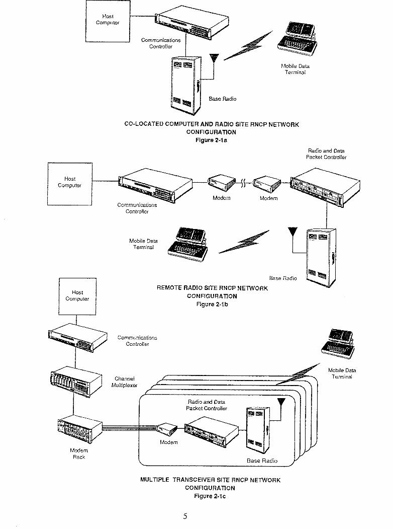
,4 diagam of some typical RXCP network topologies is shown in Figure 2- 1. Figure 2- 1 a
shows the simplest configuration which involves the host compuw and base radio being
ca-located at the same site. More complex configurations involving single or multiple
remote transceiver sites are shown in Figures 2-lb and 2-lc. From the dia, wims the
--A R N r P 7 -- neWmk is shown tr? cmsist of &i=; fdowing physical c0mponen:s:
Mobile Data Terminals (MDTs) (sec 2.1.1)
host compilter (see 2.1.2)
Communications Controller (CC) (sec 2.1-3)
Radio and Data Packet Controller (RDPC) (sec 2.1.4)
Host Computer
?nobile Data Teiminal
CO-LOCATED COMPUTER AND RADIO SlTE RNCP NETWORK CONFIGURATION
Figure 2-1 a
Radio and Data Packet Controller
IS-
Cammuniations
Mtibile Data Te:minal
Host Computer
&se Radio
REMOTE RADIO SUE RNCP NETWORK CONFlGURATTON
Figure 2-1 b
Ccrnmunications Cont-oi ter
Mobile Data Terminal
MULTIPLE TRANSCEIVER SlTE RNCP NETWORK CONFIGURATION
Figure 2-1 c
Channel Multiplexer (0 (sec 2-15)
The functions of each of the above units and their interactions with each other is discussed
in the reference subsections listed
2.1.1 MOBILE DATA TERMINALS (MDTs)
The MDTs are both the source of inbound messages to the host computer and the sink of
outbound messages originating from the host computer. The MDTs may be configured to
be mobile or portable. Each MDT is attached to a radio control unit capable of transmission
and reception of data. The data is transmitted in the form of formatted data packets, which
contain both text and c~ntrul information. Included in the conrrol information is an
identification field which allows an MDT to react only to messages addressed ro i t . A n
acknowledgement is generated by an MDT to a base radio for each error free message
received. All messages which are not acknowledged are re-transmitted by rhe
communications controller at the host site.
2.1.2 HOST COMPUTER
The host computer provides the interface to the user at the host site and is the declica~ed
centralized system controller for the mobile data communications network. From the host
computer, the user can format different classes of messages for specific mobile units. The
host computer is dircctly connected to the communications controller in the mobile d:m
network.
2.1.3 COMR/IUIVICATIONS CONTROLLER (CC)
The communications controller serves as the interface for the lMDTs to the host computer.
Attached to one end of the cornnlunications controller is the host computer and x the other
end the RDPC. The communirations controller is responsible for controlling mess ' i i g ere-
transmission and for generating acknowiedgements to inbound messages. The
communications controller performs radio control by instructing the RDPG to initiate
keying of radio transmitter sites closest to the mobile unit in a multi-transceiver
installation. The communications controller is also responsible for message formatting by
inserting forward error-correction ( E C ) to messages destined for h4DTs.

L1.4 RADIO AND DATA PACKET CONTROLLER (RDPC)
The RDPC commu~Licates via modem (leased line or dial-up) or microwave link to the CC.
Its main function is to serve as the interface to the CC for the MCTs. The RDPC performs
modulation and demodulation of inboundloutbound messages from host compuier to MDT
and vice-versa. The RDPC keys the radio transmitter at the base site under direct control
from the CC, The RDPC is also responsible for multiple access control of the radio
charms! by asserting the channel busy condition in the RNCP message protocol when
configured to operate using DSMA channel access.
2.1.5 CHANNEL MULTIPLEXER (CM)
In a compfex network requiring extended coverage, there may be multiple remote
transceiver sites which are linked together in a star configuration by a channel multiplexer
to the host computer. The channel multiplexer, in addition to providing a multiplexing
function also manages mnltiple copies of the same message received simultaneously from
the multiple trafisceiver sites by forwarding only the first error-free copy to the CC.

2.2 DATA LINK DESCRIPTION
The mobile data signal environment is characterized not only by free space losses
attributed to atmospheric propagation, but also by scattering and multi-path fading
resulting from terrestrial interaction. The phenomena of multi-path fading is the cumulative
result of reflected and scattered components of signals arriving at a receiver with varying
angles of incidence, time delay and amplitude. These parameters vary with both the speed
and location of a mobile unit and result in random phase and amplitude variations in the
received signal. Multi-path fading can result in the amplitude of a received signal varying
by up to 40 dE at a rate of 100 times per second for a vehicle travelling at 70 mph and at
radio frequency of 900 MHz. The implications of multi-path fading are that a mobile
voice or data signal suffers from high irreducible bit error rates and severe distortion in ;he
mobile environment.
Nowhere are the effects of fading more evident than in the cornrnunicarkxi between a
mobile unit and an RDPC, since signalling must be performed essentially at ground level
where a multitude of local scatterers can exist. The design of a successful mobile data
message protocol must address the effects of fading and signal distortion by employing
techniques such as data interleaving, data redundancy and forward error-correcting codes
to combat fading in the mobile environment.
The Radio Network Communications Protocol (RNCP) is m example o f a succsssftil
4800 bps mobile message protocol which has been in commercial use for several >,ears.
The RNCP protocol is used both for formatting and flow control of messages from 2 host
computer and mobile units.
2.2.1 BIT LEVEL DESCRIPTION
The RNCP protocol transmits data at 4300 bps using differential-encoded bipolar-
signalling of low pass filtered rectangular pulses. These pulses are frequency modulated
(!?-Mi by the base radio for transmission to mobile units. Differential encoded b~pcdar
signalling is pseudo-ternary taking on the values -1: 0 and +l at the symbol centre. A
binary value of 0 is represented by a zero DC level while a binary value of I is represented
by alternating positive and negative pulses. The use of alternating positive and r1egriri1.e
pulses to represent a b i n q 1 provides a built in single bit-error detection capabi1it.y since a
receiver detection error which violates the alternating pulse rule can readily be detected.
The basic RNCP waveform is a !ow-pass rectangu1a.r pulse which satisfies the firs!
Nyquist criterion for inter-symbol interference. A typical sequence of RNCP pulses is
shown in Figure 2-2, while the eye diagram for pseudorandom RNCP data is shown in
Figure 2-3. It can be seen that the noiseless RNCP pulse possesses high symmetry and is
essentially sinusoidai (2400 Hz) for consecutive values of binary 1's.
PACKET STRUCTURE
The mTCP protocol is a packet-radio message protocol. Bits are packaged into message
symbols, which are in turn arranged into RNCP messages. The RNCP protocol supplies
network and channel control information via the packetized messages in addition to text
information. The main highlights of the RNCP packet structure are listed below and are
described in folIowing sections:
mandatory message header with variable number (0-8) of text blocks
* 7 bit =;tessage symbols using 6 bit ASCII characters
Channel access control bit in the 7th bit of every symbol
* Triplicated header structure (14 RNCP symbols per copyj
BCH encoded header symbols
Reed Solomon (63,451 encoded text blocks
* Net~vork synchronization provided via special messages and tones
The general RNCP Packet strmure is shown in Figwe 2-4.
2.2.2.1 MESSAGE SYMBOLS
The bits of the RNCP protocol are used to form message symbols. Each symbol is made
up of 7 bits, of which the least significant 6 bi:s are used for the actual ASCII symbol. The
7th or mos? significant bit is used for channel access control and will he discussed later o n
ix the &script,i.=i? far channel concen&m c c n ~ d . Message symbols are transmitted itnd
received stating with the least significant bit,

Sampled W4CP data sequcnce
50 100 150 209 250 300 350 3<X) 450 503
Sample Xurnher
Figure 2-2 Typical Sampled RNCP Pulse Sequence
L e v e l
E?. 9 9.5 5 . Ei 1.5 2.0
Normalized Symbol Number
Figure 2-3 Eye Diagram for Pseudorandom RNCP Data

2.2.2.2 M E S S AGE EEADER
Each RNCP message contains a mandatory triplicated header, which is majority voted by a
receiver. The multiple copies of the header are used to provide protection during fading. A
worst case Pide duration of 20 milliseconds (one header duration) is tolerated as long as
the remaining 2 header copies are received error free.
The RKCP message header is used to provide frame synchronizatior? and conml
information to a target mobile unit. A copy of the RNCP message header is fixed length
a d is comprised of 4 symbols (28 bits) of frame SYNC codewords and 10 symbols (70
bits} of control information. The SYNC codeword symbols differ from the control
information symbols in that they do not have a channel contention control bit (7th bit o f a
symbol). The control information in the header includes the mobile !D field, a rneswge
length, nessage priority field and BCH parity check bits.
The header mobile ID field aliows a mobile unit ro react only to messages addressed to i t ,
while the message priority field allows the network to attach priority to messages. The
parity check bits are used for error detection. Each copy cf a RNCP header is encoded
with a systematic BCH error-detection code, which can detect up to 7 bit errors. .A rtczivcr
can compare received parity bits with the parity bits generared using h e rectived header
bits to determine if bit errors have occurred.
2.5.2.3 MESSAGE TEXT BLOCKS
An RSCP text block consists of 63 symbols of which 45 are actual text symbols iind the
r~mainder are Reed-Solomon (RS) parity check bits. An RNCP message can have
anywhere from a miiiimum of 0 to a max;mum of 8 text blocks. The symbols i n a test
block are norrnalfy 6 bit ASCII symbols which have been encrypted to pro~~icle a rne;rsrirt:
of security over rhe radio channel. Each text block is encoded with a (63,451 RS forward
error correction code. The (63,45) RS code can detect v errors and s erasure fills which
satisfy the equation 2v + s < 18. The Reed-Solomon code is used since i t is shoitfn to be
tffectivs for burs: enors which are chwacteris~ic of the fading mobile environment.

Message Preamble
Header (Frame Sync + 1Ox65il. symbols )
BCH encoded
Text Black 1 (63 x 6 bit symboisf
Bit 7 0
I Frame SYNC f ripiicaied (4 symbols)
-lp
I Tex? Bhck 8 (Ei3 x 6 bit symbols)
R S (63,45)
Figure 2-4 General RSCP Message Packet Structure

A sirnusoidat preamSk noomaiiy precedes the header of every RSCP rnesssse. The
prembte is esseritidfy a 2300 Hz sinusoid and is used to aifow rhz riming recovery
a'lgctr'i&rn of s receiver m q-fichmnize to incoming message md to fill in the transient
p"v,'ld on rhe radio zhmnei rvher, the 3ase r~dio is first keyed up to when i t achieves ti
steady stare ( h e trzrrsien~ s t , ~ ~ - u p me of a base radio is the order of 10-20 r - n s x ) .
Messag: preamble is nomzily nos required in systems where :tie radio is conrinuously
keysa 02.
2.3.2.5 CHASSEL COSTENTION CONTROL
The 7th bil of eye;? hzzde; 2rid rer: syraibo!, ivirh the exceprior! of the header SYNC
codewords, ronrainr a channei conrention contfo! bit or channel 'BUSY' bit. This bit is
used for contendon cizmoi r'or Digird-Sense-?tluItipIe-Access (DS-MA) channel protocols.
The busy bit is i g i o ~ d far ALOHA E CCShIX channel radio chznnei access protcxols.

Figure 2-5 RKCP Network Idle Tone

3. ARDPC OVERVIEW
3.1 FUNCTIONAL REQUIREMENTS
The functional requirements for the AlRDPC may be class ;ified as being eit :her core or
extended functional requirements. The core functions are required in order to maintain
compatibility with the first generation design and are considered to be essentiai for the
operation of an RDPC. The extended functions represent desirable but non-essential
featwes. The extended functions in general represent convenience improvements over the
first generation design. Some extended functions are derived from first-hand field
experience with the first generation units, while others are the result of the need to
ar,iicipe Fdiure reqiiirernenrs.
T'ne i i h * ~ r ' functional requirements for the AEiDPZ are summarized h i o w . The description
for a hs~ed requiremenr is given in rhe reference subsection indicated:
CORE FUNCTIOXS
1, mduIatior4idemodt;ia~ofi of RXCP message data toffrom mobile units (sec 3-1.1)
2. communications with tIIe CC via modern link (sec 3,1.2)
3. control of the transceiver sire radio (sec 3.1.3)
3. C O ~ E O ~ of radio channel access for mobile units (sec 3.1.4)
EXTEXDED FCKCTIOSS
1 . tWEbus capabi!i:y
2. s i f ~ p ~ f t fur a user in~erface lo a local consoie '3 3. improved user diagnostics
4, adjusmcnt of modem sign& !eveis from a k a ! console
5. FEC decoding of messages
6. genemion of radio chmnei e m r statistics
7. RYCP message monirosng capzbili:y
8. RF a T m s and RSSf signal monitoring
9. output of rnorse coded stabon id (CWID)
(sec 3.1.5)
(see 3.1.6)
jsec 3.1.7)
(sec 3.1.8)
(sec 3. ! .9)
(sec 3.1.10)
jsec 3.1.11)
(see 3.1.12)
(sec 3.1.13)
3.1.1 MODEM FUNCTIONS
An RDPC's primary function is to provide modem capabilities at a rransceiver site for
packet-radio mobile data communications. The RDPC is responsible for demodulating
inbound messages from mobile units a ~ d modulating outbound messages originating from
the host computer or CC. Demodulation involves recovery of transmitted data clock,
transmitted data and frame synchronization. Modulation involves convening a s e d bit
stream into analog pulses for transmission over the radio link.
The CC is the source of acknowledgements to messages received at :he host computer sire
and is the preprocessor for outbound messages generated from the host computer. In most
cases, a transceiver site is situated away from the host computer site and the nerwork may
consist of many transceiver sites, each with its own bass radio. In such a case, each
RDPC is connected in a star network conf gtiration to the CC via a GM. Each RDPC in the
network must then communicate remotely with the host computer site via rhe CC using a
leased-line or dial-up mudem l ink
3.1.3 TRANSCEIVER SITE RADIO CONTROL
The RDPC is responsible for radio controf at the transceiver site. The controller keys the
base radio under remare control from the host site or under local conm! ar the trailsceiver
site. The keying of the bass radio coincides wirh outbound messages, which nwsr be
transmitted from a particular transceiver site.
3.1.4 RADIO CWANKEL ACCESS CONTROL
The R3PC is responsible for chmnei xccss control for DSMA based contention schemes.
In DS-MA based systems, the RDPC is responsible for setting and cIearing :he inbound
chmnd busy bit ia the R-ZCI? mersa~t: v pm!ocoT. A mobile wit u s i ~ g DCMA ctlanne!
access senses the state of the bit before attempting to transmit a message inbound 10 the
host computer. A mobile unit is inhibited from transmitting until the channel access bir is
cleared, Channel contention control is desirable for minimizing the number of corrupted
messages that result when multiple mobife units access a common radio channel

simultaneously. iMinimizing the number of corrupted messages increases the channel
throughput by reducing the number of re-transmissions over the network.
3.13 VMEbus CAPABILITY
The A,'IDPC motherboard is required to have the capability to operate from an industry
srtlndard VMEbus. This function allows the ARDPC to be rack mounted and integrated
with other comrnunicatkms devices using a VhEbus.
3.1.6 USER CONSOLE INTERFACE
The ARDPC is required to provide user access to all critical operaring and channeI status
paranwters from a local console, All critical ARDPC operating parameters should be
adjusrtible from the user console. Afi operating information and channel status information
should be available for a repon display onto the user consofe. The user consok interface
function represents a significant improvement over the first generation RDPC, which
codd only pass operating state information via front panel LEDs.
The first generation controfler had only front panel LEDs to reflect hardware fault
cofidirions. The ARDPC is required to provide better and more intelligent diagnostics for
rhs hardwzre platform. The diagnostic tests should include loopback tests of the CG and
RF data links and should be initiated on user demand from the console interface.
3-1-8 LEVEL ADJUSTMENTS FROM LOCAL CONSOLE
The f ~ s s generation RDPC's inpar and output signal levels were adjusted by physically
accessing po:en:iometers on rhe controller board. As a convenience feature the ARDPC
AZOD, DISC and 3IORSE code signal level adjustments are to be made from a Iocal
cwrnie rather than frnm &e hardware, This avoids &_he chore nf opening the chassis and
accessing adjustment porentiome~ers to tweak the hardware. This feature is possible only
because of DSP being used to process input and output signals,

3,1,9 FEC DECODING OF MESSAGES
The first generation controllers were essentially dumb modems which lacked the
intelligence to perform message processing at the controller level. This resulted in ail
received inbound messages being passed to the CC regardless of condition, thus placing
an unnecessary load on the CC. The ARDPC is required to perform message processing
using FEC decoding to filter out corrupted messages and to generate error statistics.
Message filtering helps to minimize unnecessary message traffic to the CC thus reducing
the processing load on the CC.
3.i.10 RADIO CHANNEL MONiTORING
The ARDPC is required to generate and log error statistics for RNCP messages
transmitted and received. Generation of bit and packet error-statistics are useful i n
analyzing and tuning an RDPC within a network. The earlier RDPCs provided no
indication of the number of messages rejected or received or the number of errors
occurring in the inbound message text-blocks.
3.1.11 RNCP MESSAGE MONITORING
A means of echoing or dumping messagcs rlowing through the ARDPC is a convenience
feature which is valuable in analyzing a network. This feature is made possible by
introducing message processing at the ARDPC level, which previously did not exist. The
messages monitored must include aH messages received from the CC for output onto the
radio channel and all messages received demodulated from the radio link.
3.1.12 R F ALARMS AND RSSI SIGNAL MONITORING
The ARDPC is required ro sample and log the RF atm signals if available. A base statior!
radio may have outputs for RF a l m s , which provide an indication of the VSWR (Voltage
Standing Wave Ratio) on the radio channel and hence provides information on the quality
of the radio and antenna system

3.1.13 CWID OUTPUT
Each RDPC in fieid operation is required to transmit station identification for regu!atory
agencies such as the FCC in the U.S. or DOC in Canada. This station identification can be
in the form of' voice or Morse coded call letters which conform to FCC regulation 90.425.
The A D P C wiii use morse code of a single tone frequency to generate the station
idenrificarion suing.

3.2 HARDWARE ARCHITECTURE
The improved inteiiigence required for the ARDPC made it necessary to base a large
degree of the functionality in software rather than hardware, A software design is
inherently flexible and is better suited for the complex processing required for supporting
the extended functions presented in section 3.1. The use of a microprocessor in the
hardware design is fundamental for the implementation of an embedded software
architecture. To address the need to support different modulation/demodulation schemes as
detailed in the requirements and also facilitate the fast number crunching required for
digital modem functions, it was decided to aIso incorporate a DSP processor for the
modem functions.
A DSP processor with ADCs and DACs is able to convert functions previously
implemented with analog circuitry, such as filtering, to be replaced with digital operations.
The use of digital rather than analog operations retains the full benefits associated with
digital circuitry, namely stability, precision and testability. A software based DSP modern
provides a significant advantage because a change in the moduIation/dernodulation scheme
can be implemented in software, without a change to the basic hardware. A single platform
is thus able to support many different protocols, which provides a cost savings in design
effort. DSP processing is also able to perform operations not possible in the analog
domain. For example, analog level adjustments with a DSP processor can be made using
sofrware employing a user interface to a local consoie.
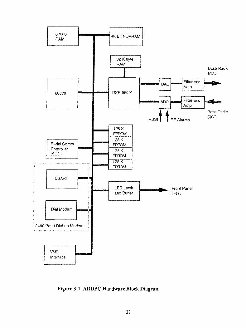
The final ARDPC hardware block diagram is shown in Figure 3-1. From the figure, it can
be seen that the ARDPC features a duo-processor design utilizing a Motorola 58000 32 bit
microprocessor and a Motorola DSP-56001 processor. The main function of the DSP
processor is to perform the modem functions for the ARDPC. The DSP-56001 is slaved
to the 68000 microprocessor which serves as the central control processor.
Communication between the two processors is conducted via the 24-bit wide Host
Interface port of the DSP-56001. The Host Interface port is a peripheral device within the
DSP-56001 and appears as a memory mapped device lo the 65000 micrcprocessor. The
Host Interface port is equipped with a variety of control logic to allow the two processors
to transfer data using interrupt or pofling contrd.
Controller
Dial Modem D 2400 Baud Dial-up Modem
4K Bit NOVRAM
Base Radio bwD
Base Radio
RSSl t f RF Alarms DISC
LED Latch Front Panel and Buffer EDs
Figure 3-1 ARDPC Hardware Block Diagram

3.2-1 DEVICES UNDER 68009 CONTROL
The 68000 microprocessor controls 512K of UVEPROM which is used as storage for
both 6 8 0 and DSP-56901 code. It also accesses a battery backed RAM and 4K-bit non-
volatile RAM (NOVRAM) which is used for storing data that must be involatile such as
the ARDPC configuration or database parameters.
The 68000 communicates with the user console via a SCC chip or dial-up modem which
allows remote access to the ARDPC. The 68000 microprocessor is interfaced to the dial-
up modem via a USART chip which is under control of the 68000 control processor. The
68000 also controls a bank of fiont-panel Light-Emirting Diode (LEDsj indicators which
may be used to signal different states or conditions of the ARDPC
A VME interface chip is provided to provide expansion capabilities fcr the circuit board or
alIow the card to be inserted into a VMEbus device. This chip is used to satisfy the
auxiliary requirement for W b u s capability.
3.2.2 DEVICES UNDER DSP-56001 CONTKOL
The DSP-56001 processor is independently progrzmnable and has access to 32K of
external 1 wait state RAM for executing DSP programs. The actual DSP-5g001 executable
load is stored alongside the 68000 microprocessor software lozd in the 512K of
UVEPROM. This memory is accessible only to the 68000. The DSP software must be
transfened by the 68000 microprocessor from UVEPROM memory to the DSP-56001
processor R4M via the Host Interface port during a bootstrap load,
The DSP-56001 duectly accesses one digital to analog converter PAC) and two analog to
digital converters (ADCs). One of the two ADCs is 8 bits wide and is multiplexd to
sample the RF alarm channels and the RSSI signal from the base radio. The remaining
ADC and the DAC form a set of 12 bit ports for the transfer of demodtilauon/modcllation
data samples to/from the DSP processor. The demodulationlmodulation ADCDAC pair is
clwked by the DSP processor to input or output data at a sarnpk rats of 7 6.8 kHz. This
pair of convemrs yields a dynamic range of 72 dB.

The analog demodulation/moduiation signals entering or leaving the ARDPC are low
passed filtered by a front-end 4 pole analog Butterworth filter with a cut-off frequency of
9.5 kHz. This cut-off frequency was chosen to accommodate poieiiiial trpgiades to a 9.5
kbps data protocol. However, the analog cutoff frequency implies that the DSP processor
must provide additional digital filtering for a 4.8 kHz data protocol such as the RNCP
protocol,

3.3 DSP-56001 SOFTWARE REQUIREMENTS
The question as to which processor is responsible for what function natwalty arises in a
multi-processor design. The A m P C software functionality that was eventually assigned
to the 68000 microprocessor or the DSP-56001 processor was determined largely by
considering which processor was best suited for a particular task. In some instances, bctfi
prmessors were equally suited for a particular function and the decision was arbitrary in
assigning the function.
In the ARDPC, the 63000 microprocessor was assigned a master processor role simply
because it was best suited for managing data and for making decisions. The 68000 was
also best suited to implement a user interface from a local console because of the on-chip
serial devices available. The DSP-56001 was assigned a slave-processor status in order to
free it to become an arithmetic processing engine. This subordinate role allowed the
ARDPC to take advantage of the superior arithmetic capabilities of the DSP-56001
processor. Consequently the DSP-56001 processor was assigned computationally
intensive operations such as modulation and demodulation of data and generation of tones
for continuous-wave identification (CWD) output.
The software requirements for ~ l e DSP-50001 are grouped using the following categories:
General Operational Requirements
Inbound inessage processing
Outbound message processing
* Console adjustments
RF alarm and RSSI signal monitoring.
The sofhvare requirements assigned to the DSP-56001 are Iisted below. A description for
each requirement may be found in the listed subsection.
GENERAL OPERATIONAL REQUIREMENTS
1. Inter-processor communication with the 68000
2. POST diagnostics
3. Full duplex modem operation


The DSP-56001 must provide a basic set of "power on self test" {POST) diagnosdcs for
detection of haf&hiare faults on startup. The foliowilg standad rests should be included:
* RAIV test
checksum of DSP-56001 c d e
Intempt clock rate test
ADC diagnostic
Andog filter diagnossc
A read/w&e/verify diagnostic rzf $1 internal and external static RAM should bc performed
prior to downloading DSP-56001 code. A running checksum should be ptrfolmed or; all
DSP-56901 inswtcdons :~.itlen 10 p r o g m memory to verify the inlcirfitv - a of the code.
Diagnostics need to be provided for verifying the rate of 3 2 Iniermpt ckxks, the accuracy
of the various ADCs m d the cccuraey of the analog low pass filter.
The POST diagnostics shodd be iniGated by the 68000 using the HI porr message
interface. Any failwe of POST diagn~srics should be reponed to :he 6800 using rhc same
interface.
3.3.3 FULL DUPLEX MOT?ET\I CfPERATfOW
The ARDPC ausr be able ro perform full duplex 4800 bps operarion using the RSCP
message protocol. Bow of messages to from the radio chmnef must be limited by
the radio channel and not the RDPC In full ditpkx operation. The ARDPC ivil1 be
configured for fuff or half duplex operation &om the user console,
The DISC line of the base radio stippiies ;he baseband signal from rhe base radio
discriminasor. The DSP processor is responsible for sampliflg rhe DISC fioz of he bast.
radio. Tne data is sampled at 76.8 kHz by the hardware to provide an oversampiing rario
of 16 to I . The sampling insrances are determined by a sampling cluck whose signs1 is
used to genzrare inrenupts to &e DSP prcxessor.

3.3.5 LOW PASS FfLTERIlVG
The smpled DISC signal must be low pass filtered by the DSP prucessor to reduce out of
band noise in the f ~ q t e n c p range 2.d - 9.6 H z , Frequencies above 9.4 kHz are filtered
by the front-end analog Euttenvofi~ filter in the ARDPC hardware. The cutoff frequency
of the analog filter is chosen so that a 9.6 kbps data rate can be supported by the ARDPC.
3.3.5 DC OFFSET REMOVAL
The A W P C is AC coupled ard therefore possesses a finite recovery time for a DC step-
input. Such a step input is present under normal op-ating conditions when the base radio
encounters the stmup of a carrier signal on the radio channel. The preseme of DC in the
DISC signal has adverse effects on dgoridms which rely on fixed DC thresholds for
operation. Some fom of DC-offset recovery must be implemented for such algorithms.
3.3.7 BIT TIMING RECOVERY
The DSP-56001 must self-synchonize to the data and the algorithm chosen must be able
to adjxt for jitter in the timing signal once a lock has been established on the symbol
centers of the bit stream, The ESP-56001 must buffer samples of the bit stream in order
for the timing recovery dgorithm to sesrch for the the besr decision sample within the
available samples.
3.3.8 BIT DECISION
The received data birs are elements in the domain f - i ,O , f 3 because of the pseudo-ternary
n a m e or" the RXCP baseband signal. The data recoveqr algorithm musr differentially
decode the ~ s s m i n d bit sequence and map ire bits into the domain f 0,1)
The DSP processor rnusr deremine message boundaries from the serial bit strehm by
scmning the received bit smm %'or the SYYC bit pattern in rhe RNCP message protocol.
The SYNC pattern is zip!ica~ed in a RNCP messzge header and consists of 28 consecutive
Sits uniquely defined for the RNCP protocol. A condition of message SYNC is
established if a rnajoriry vote of a sequence of scanned bits are equivalent to the SYNC

bits. Once the SYNC codewords are located, the symbol boundaries are known and the
bits of the message header arid text blocks may be grouped into 7 bit RSCP symbols. The
extracted symbols rnusr be buffered by the DSP-56001 for post-processing.
3.3.10 MESSAGE HEADER PROCESSING
The DSP-56001 is required to perform BCH decoding on each extracted message header
to determine if the message header contains bit errors, The RNCP message header is
received in triplicated fom and msst be de-triplicated by using najority voting before
BCH decoding can be performed. A message header will be labelled 'good' if the
operation of BCH decoding results in no errors otherwise the header will be marked 'bad'.
The text portion of a message with a bad heder will be discarded and oniy the header wiH
be forwarded to t'ne 65000 microprocessor.
The DSP-56001 is required to nansmit a recavered RNCP message in header and text
block segments to the 68MXI. Each header or text block will be fkamed with a sequence of
bytes in the form of a 680013 message to identify the start and end of a header or text block
segment. The extracted header of all messages will be ~ansmitted to the 68000 but no text
is to be sent with a message with a bad header.
3.3.12 PULSE SHAPING
The DSP-56001, upon command from the 68000, will receive outbound RTCP messages
in header and text blvck segments for generation of pulses for output onto the radio
channel. The messages appear to the DSP-56001 as a serial bir stream packetized on by re a hn* boundaries and on header and text block segments. A distinction must be madL trL~ween
header or text data because all symbo!s of a RNCP message have busy bit information
svith h e exception of the SYNC codewords of the RNGP hezder.
Each output pulse for a bit will be oversampled by a facror of 16 (i.e. 16 modulation
samp!es per puke). Each RNCP symboi will be received on a byte boundary from the
68336 wit'rr only rhe least significant 7 bits being part of the symboi. The bits of each
symbcrl will be modafated starting with the least significant bit and progressing towards
the most significant bit,
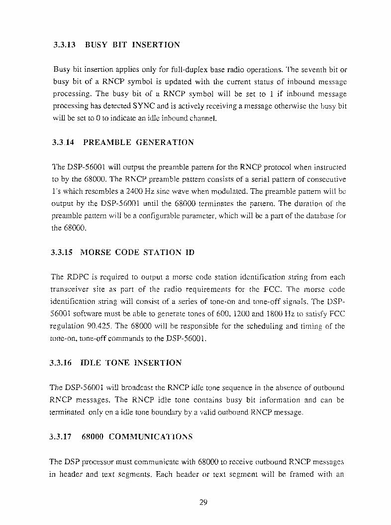
3.3.13 BVSY BIT INSERTION
Busy bit Lisertion applies only for full-duplex base radio operations. The seventh bit or
busy bit of a RWCP symbol is updated with the current status of inbound message
processing. The busy bit of a RNCP symbol will be set to 1 if inbound message
processing has detected SYNC and is actively receiving a message otherwise the busy bit
iiiill be sst 10 0 to indicate m idle inbound channel.
3.3.14 PREAMBLE GENERATION
The DSP-56001 will output the preamble pattern for the RNCP protocol when instructed
to by the 68000. The RNCP preamble pattern consists of a serial pattern of consecutive
1's which resembles a 2400 Hz sine wave when modulated. The preamble pattern will be
ourput by t5e Df P-5OOOf. until the 58000 terminates the pattern. The duration of the
preamble partem will be a configurable parameter, which will be a part of the database for
the 68000.
3.3.115 MORSE CODE STATlON 1D
The D P C is required to ouput a morse code station identification string from each
~ransceiver site as part of the radio requirements for the FCC. The morse code
identification string will consist of a series of tone-on and tone-off signals. The DSP-
56001 software nust be able to generate tones of 600, 1200 and 1800 Hz to satisfy FCC
regulation 90.425. The 68000 will be responsible for the scheduiing and timing of the
me-on, tone-off commands to the DSP-5600 1.
3.3.16 IDLE TONE INSERTION
The DSP-50001 will broadcast the RXCP idle rune sequence in the absence of outbound
RSCP messages. The RNCP Idle tone contains busy bit information and can be
terminated only on a idle tone boundary by a valid outbound RNCP message.
The 35P processor must cornmanicate with 68000 to receive outbound RNCP messages
in header and text segments. Each header or text segment will be framed with an

identification string to identify each segment, The DSP processor will acknowledge the
completion of the rnodulatim of message. The DSP processor will warn the 680QO of an
modulation data undermn condition with an undermn message to the HI interface.
3.3.H CONSOLE ADJUSTMENT OF SIGNAL LEVELS
A desired improvement of the ARDPC was to make the adjusrment of critical levels
possible from the user console instead of having to tweak a potentiometer on the actgal
hardware. This feature is made possible by the use DSP in the modem because analog
output levels are directly related to the digital levels input to the DACs. The MOD and
DISC levels can be adjusted by simply applying a gain value to the MOD and DISC
processing algorithms. This gain can be specified by a user from the user console and can
be transferred to the DSP processor by the 68000.
3.3.19 RF ALARM AND WSSf SIGNAL MONITORING
The DSP-56001 is responsible for periodically sampling and processing various RF
alarms and the RSSf signal from the base radio. The RF alarms provide an i::ciication of
the volage standing wave ratio on the rauic channel and provides information on the
quality of the radio and antenna system. The DSP-56001 must buffer the current samples
taken and be able to provide the values on demand to the 68000.
The Radio Signal Strength Indicator (RSSI) provides infonnaricn on the relative stsength
of the received radio signal. The level of this signal is useful for applying antenna chversity
and for quantifying the quality of tFle received dzta

4.0 DSP-56001 SOFTWARE ARCHITECTURE
4.1 CONTEXT BVERVfEfV
The context diagram far the DSP-56001 processor is shown in Figure 4-1. From the
d i a p m ?he foifowing inputs and outputs are identified:
INPUTS
1. control signal from the sample rate (76.8 Hz) clock
2. control signal from thc bit rate (4.8 kHz) clock
3. dam and conoc! infomation from the 6800C
4. data from RF alarms and RSSI signal
5. data from the DISC output of the base radio
OUTPUTS
6. data and control information to the 68000
7. data to the MCID input of the base station radio.
(sec 4.1.1)
(sec 4.1.2)
(sec 4.1.3)
(sec 4.1 -4)
(ssc 3 . 1 3
(sec 4.1.6)
(sec 4.1.7)
A description of each of the above inputs and outputs is provided in the reference sub-
section provided.
4 . SAMPLE RATE CLOCK (75.8 kHz)
The sample rate clock signal is used by the DSP-56001 to control the sampling of inbound
and otrtbound radio channel dxa. This clock signal provides intempts to the DSP-56001
ar a numinal rate of 76.8 kHz. The DSP-56001 intempt service routine tisr) for the
sample clock interrupt inputs samples from the DISC output of the base radio and/or
outputs sanples of the baseband modu1a;ion waveform to the MOD input of the biisc
radio.

4.1.2 BIT RATE CLOCK (4.8 kHz)
The bit rate ctnck signal is prr?vi&d to synchrwize activities which must be cornplc~ed a: a
symbol or bit time. This clock signal is used to generate interrupts in the DSP-50001 at a
nominal rate of 4.8 kWz and is derived from the sample rate clock sigm!. The DSP-56001
intenupf service routine (isr) for the bit rate clock performs operations which are critical at
the bit rate. These activities include generation of samples for the baseband modu!ation
waveform and maintenance of the internal DSP software clock.
The control processor (68000) supplies control and data information to rhe DSP
processor. All communication between the two prucessors is asynchronously rranxicted
via the Host Interface (HI) port of the DSP-56001. The HI port contains double-buffered
full duplex data registers with different handshake protocols to facilitate the ~ransfer of
information between the 68000 and DSP proc, P ~ ~ ~ r s .
Control information transacted from the 68000 is in the fom of coded message directives
formatted in packets of 24 bits. Data transferred frorn the 68000 includes header and rest
block segments of RNCP messages received by the 68000 from the cornrnilnic?t' i, inns
controller.
4.1.4 R F ALARMS AND RSSI
The DSP-56001 is required to sample the RF alarms and RSSI signals periodicaliji. The
RF alarms provide an indication of the Voltage Standing Wave Ratio (VSWR) on the radio
channel and hence provides information on the quality of rhe radio and antenna sFsrern.
The RSSI provides informztion regarding the relative strength of an inbound radio signal.
43.5 FM DISCRIMINATOR
The FM discriminam (DISC) stlpplies the znahg: baseband RNGP data signal whefi data
is being received. The DISC signal is filtered by an analog low pass filter bzfore being
sampled by ?he DSP-56001. Each received inbound pulse representing a bit is converted
by sampling into a sequence of 16 digital samples by the ADC connected to the DSP-
.%OOl.

The DSP processor supplies data and control information to the 68000 via the HI port.
The control information is in the form of processiiig siaius and response messages to
commands initiated by the 68000. The data transferred includes demodulated RNCP
messages in header and text block segments. The RNCP headers are left in triplicated
format and are BCH decoded before being passed to the 68000.
3.1.7 MODULATOR
The DSY-56001 writes the. MOD DAC with modulation samples which are converted to
analo~; ... waveforms and are senr to the MOD input of the base site radio. The base radio
then frequency shif~s the spectrum of the data to the desired carrier frequency.

ToiFion Conmi Frocesso: via HI ?on
Sample R a e Clock (76.8 Wz!
Figure 4-1 DSP-56001 Context Diagram

4.2 LEVEL ZERO SOFTWARE DECOMPOSITXON
The DSP-56001 software at the highest level consists of 5 essentially independent
routines; two of which are interrupt driven. The data and control flow diagram for the level
zero modules is shown in Figure 4-2. The following modules are identified:
LEVEL ZERO MODULES
I . BOOT (Bootstrap Loader) (sec 4.3)
2. I 0 (Sample Rate isr) (sec 4.4)
3. SC (Bit Rate isr) (see 4.5)
4. DIAGS @iagnostics I-landler) (sec 4.6)
5. MAIN (Main Back~ound Processor) (sec 4.7)
BOOT is the bootstrzp loader for the OW-56001 software and executes only afier a m e t
or power on condition m transfer code to the DSP-56001 memory. 10 services the 76.8
kHz sample rate intempt to transfer data toiffom the modulator DAC and the discriminator
ADC, SC services the 4.6 kHz bit rate intempt and performs the processing which need
ro synchronized at the symbol rate. DIAGS performs a set of user specified hardware
diagnostics for the ARDPC. MAIN is a main backgsound processing task which performs
the processing which is not time critical in the DSP-56001.
The fonnai decamposi~ion of the level zero modules is provided in the reference sub-
section ifidicated. A description of the data stores in Figure 4-2 is provided in section 4.8
which describes the data dictionary.

- Daia30w
.... . . ..... . . . . ... . . . .. . ..... . .... . Contro! Flow
Figure 4-2 Level Zero Software Decomposition

The decomposition of BOOT consists of a single level only.
BOOT is an mdependent program which executes only after a power-on or hardware
RESET condition. The main function of BOOT is to perform power on self-test (POST)
diagnostics and the loading of the DSP-56001 main application code into external DSP
RAM.
The DSP-56001 enters into a special bootsnap mode of operation upon power-up or reset.
An intrinsic ROM based bootstrap program executes within the DSP-56001 while in the
bootstrap mode. This resident program polls the HI port continuously for data from the
68000 processor and transfers any data received from the port into DSP-56001 internal
memory. The 68000 processor is responsible in bmtstrzp mode for retrieving BOOT code
from the UVEPROM and for transferring it to the DSP-56001 via the HI port using the
intrinsic bootstrap loader. The transferred BOOT code automatically begins execution at
the DSP-56001 starting address of $40 hex upon the completion of the BOOT code
transfer.
BOOT executes by initially performing POST diagnostics to determine if i t is safe to start
the transfer of the DSP-56001 main application code from the 68000. The main application
code is transferred from the 68000 into external DSP-56001 RAM by BOOT if the POST
diagnostics pass otherwise a fatal error condition is communicated to the 68000. The final
operation by BOOT is to branch to the main application code which ne-~er again executes
BOOT.
4.4 DECOMPOSITION OF I 0
The mcdule 10 consists of a single level only. The data and control flow diagram fix 10 is
shown in Figure 4-3.
fO services thc 76.8 kHz sample interrupt in the DSP-56001. I 0 takes advantage of the
fast intempt capability of the DSP-56001 and consists of 2 instructions. One of the
insuucrions is used to read a sample from the DISC ADC and transfer i t to the input data
queue fIhTFQj while the second instruction writes the MOD DAC with a sample from the
modulation data queue (MODSQ). In order to facilitate the use of the DSP-56001 fast

interrupt, a pair of hardware registers are permanently dedicated to INPQ and MODSQ to
serve as input and output pointers respectiveiy.
Sample Rate Ciock
NPQ
-b Data Fciw
I.... . ....................... ... >:>:.:... Cornrol r low
Figure 4-3 Data and ZontroE FZow for 10

4 5 DECOMPOSITION OF SC
SC services the 4.8 H z bit rate ktemp: and is responsible for generating the modulation
data samples for output to the MOD DAC. SC is decomposed into 2 routines which are
specific to the type of modulation data being processed. The 2 routines are
SC-msg-server and SC-morse-server. SC-msg-server is responsible for generating
modulation samples for the idle tone, message preamble and RKCP message data.
SC-morse-server is responsible for generating the pure tone signal for the morse code
station id. Only one SC routine executes at any one time. The vectored address for the bit
rate clock isr is wrirren with the address of either SC-msg-sewer or SC-morse-server.
Which address is written is determined by the modufe MAIN which interprets comrnmd
messages and performs modulation data management. During normal processing
SC-rnsg-server wil: be senicing the symbol clock interrupt. SC-morse-server will
senlice the symbol isr when the 68000 schedules the output of the morse station id.
4.5.1 SC - msg - server
The data and control flow diagram for SC-msg-server is shown in Figure 4-4.
SC-rnsg-server communicaces with the background software via the S CTRAN S data
store. This data store is under the control of the background routine MAIN-rnword-crrl
which 4s responsible for scheduling and managing the data which is to be modulated by
SC. SC-TUNS contains both data and eonirot information for SC-msg-server.
The CONFIG and CTRL-FLAGS data stores contain the essential DSP-56001
configuration infomation for the ARDPC. The CONFIG and CTRL-FLAGS data s w e s
supplies the modulation gain and the state of the channel busy bit for SC-msg-sener.
Xoduiation sarnpies generaced by SC-msg-server are initially pfaced in the
SC-SERVERQ which contains 16 samples (1 bit time) of data. The procesbing in
SC-msg-server is pipelined so thaf it mnsfers a buffer of samples from SC-SERVERQ
ro the mdularion data buffer (MODSQ) 2nd also refreshes SC-SERVERQ each time it is
emptied.

4.5.2 SC - rnorse - server
The data and cnnm: flow biagam fsr SC-zorse-server is shown i n Fizute .... 1-5.
SC-morse-server communicates with the background via the MORSECMD common
section. MORSEChID is under the contrd of t x backgo~nd routine hlAIN-rnnrse-c:f
which is respoilsibie for scheduling and controlling the rnorse code paltern to be oarptlt by
SC-morse-server.
The ,M0RSESMP data store is anaiogcms to SCSERVERQ in SC-msg-senw tihile rhe
CO3'FIG %id CTRL-FLAGS serge &e same purpose for SC-mttrsz-ssnm- as they do for
S C-msgserver.

Figure 1-4 Data and Control Flow for SC msg server - -
Figure 3-5 Data and Controf Flow for SC rnorse sewer - -
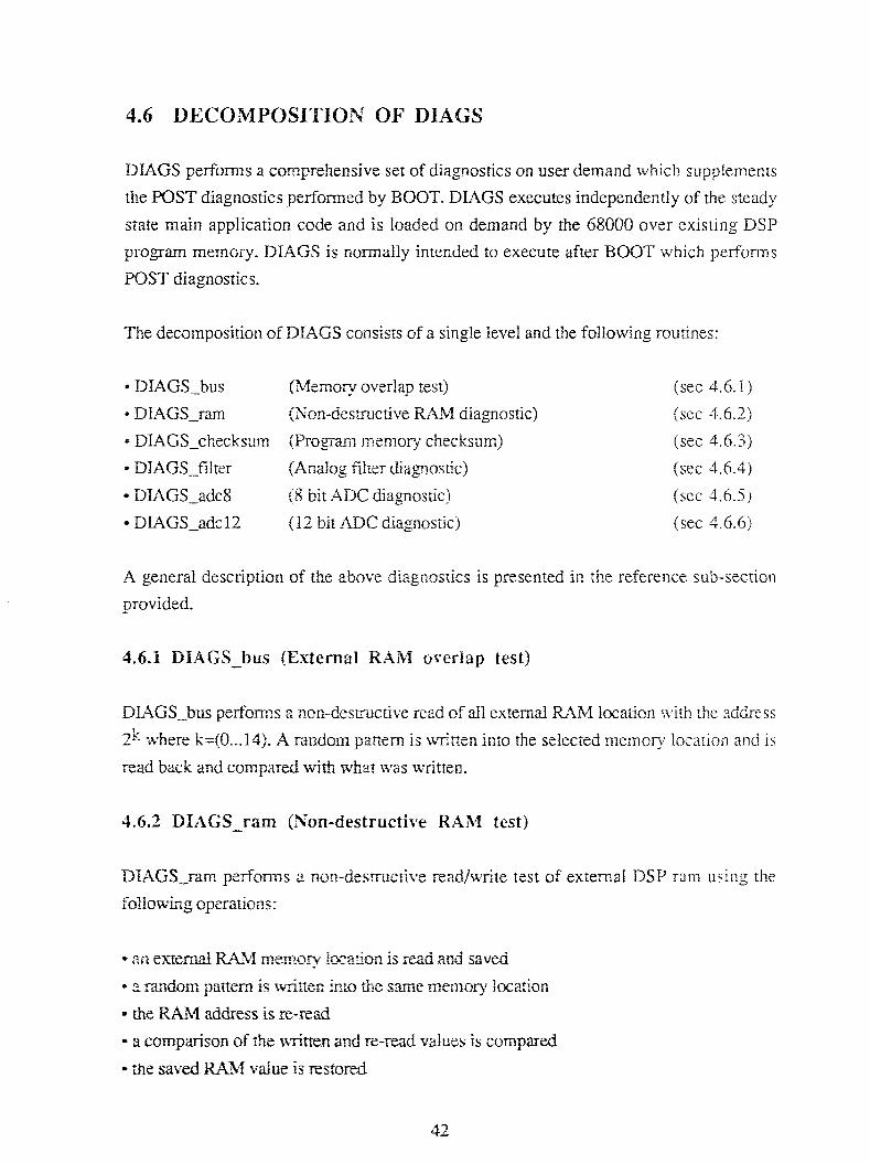
4.6 DECOMPOSITION OF D U G S
DIACS performs a comprehensive set of diagnosacs or! user demand which supp!ernents
the POST diagnostics performed by BOOT. DIAGS executes independently of the steady
state main applicaeon code and is loaded on demand by the 68000 over existing DSP
program memcry. DUGS is normally intended to execute after BOOT which pzI-iComs
POST diagnostics,
The decomposition of DLAGS consists of a single level and the ijIloiving routines:
DIAGS-bus (h4crnory overlap test)
DIAGSrm (Son-desmctive RAM diagnostic)
* DIAGS-checksum i'Propxi memory checksurn)
DfAGS-filter (Amlog f i l ter &agnostic j
DfiZGS-adc& (8 bir ADC diagnostic j
DUGS-adc 12 (12 bir ;V)C diagnostic)
fsec 4.6.1)
(sec 4.62)
(sec 4.6.3)
(see 1.6.4j
(sec 1.6.5)
(see 4.6.6)
A general dsscripticln of the above diagizosdcs is presenred ir, the reference subsection
provided.
4.6.2 D fAGS - ram (Nan-destructive RXhf test j

4.6.3 DIAGS - checksum (Program checksum diagmstie)
DIAGS-checksum performs a checksum of DIAGS software by slamming all program
words modulo 24 hits. The grand total is then added to a value supplied via a command
message from the 68000 and if the resultant sum is zero the test passes otherwise it fails.
4.6-4 DIAGS - filter (Analog filter diagnostic)
DIAGS -filter tesrs the quality of the analog low pass (9.6 kHz) filter of the ARDPC. A
series of pure test tones u e generated above and below the cut-off frequency of the analog
;ow pass filter. These tones are generated with the aid of the internal SINE RQM table of
rhe DSP-56001 a d are r?orninatly set at 6982, 7680, 85333, 9600, 10971, 12800 and
15360 Hz (based on SIXE RUM table skip factors of 11, 10, 9, 8, 7, 6 and 5
respzctively).
Samples of each tone are sent to MOD and the signal is looped back to the DISC line of the
ARDPC. The pe& vafce ourput from the filter for each tone is found and compared
agains~ rckrence values based on h e filter components,
46.5 DIAGS - a d d (8 bit ADC linearity test)
The 8 bit ADCs of ~'ne ARJPC are ~ s e d for inputting analog RF and RSSf values into the
DSP-SCiOOl. DTACS-add3 tests the integrity of the 8 bit ADC by looping back a reference
tone through the ADG and comparing the read digital values with reference values. A
pass/I"aii co~dition is returned to h e 68000.
4.6.6 DlAGS - adel'? (12 bit ADClDAC diagnostic)
The 12 bit ADC and DAC of the ARDPC are used for sampling MOD ar.d DISC data for
inpur and ourput data onto the radio channel. DIAGS-adcl2 tests the integrity of the ADC
and DAC pair by generating a 300 Hz waveform with the aid of the DSP-55.001 SINE
ROM, ourpur~ing the samples to the MOD DAC, looping back the MOD signal through
DISC and reading back the samples from the DISC ADC of the ARDPC. The digital

values written to MOD DAC are compared against the digital values read back from DISC
Af>C and a passlfaif condition is resumed to ~ + e 68000.

MAIN performs the processing which is not time ciirical in the DSP-55001. This includes
the following:
* responding to 68000 commafids via the HI port
receiving and preparing RNCP data received from the 680UO for the outbound channel
a processing iaput DISC samples
* processing channel state information
transfer of extracted inbound RNCP data io Ihe 68000
f YNC bstec~on and majority voting of bYCP message data
alignment of inbound RNCP data bit stream onto byte boundxies
BCH decoding of inbound header data
At any time some or all of the above rasks wi!l be waiting to be performed. The logic i n
h'fAIN polls the number of tasks waiting to be performed and distributes the processing
rime evenly amongst the tasks to avoid any single task from monopolizing the available
processing bandwidth. Operations perhrmed by MAIN are interrupted regularly by both
SC and 10. Both isrs transfers conzol to M A N upon completing execution. . .
The decomposirion of AIAfiu' consists of 3 levels which are discussed in sections 4.7.i to
4.7.3 .
3.7.1 LEVEL 1 DIECOMPOSITIOX OF MAIN
The Ievel 1 data and comoi flow diagram for MAIN is shown in Figurc 4-6. From the
diagram it can be seen that MAIN is decornpused into the follclwing level 1 modules:
1. &MIX-ctd (kIA4fN con trot routins ) (sec 4.7.1.1)
2. Pc4AIN-init (DSP-56001 global initialization routine) (sec 4.7.1.2)
3. MAIS-HInc (HI port receive data manager) (sec 4.7.1.3)
These m~dt?!es a e discnssed i~ rhe reference subsections provided.

4.7.1.1 MAIN - cerf (MAIN control routine)
-MIN-ctrl coordinates all background processing activities which execute when the
sample and symbol isrs are not active. These activities include the following:
DISC data processing - 68000 command processing
RF dann and RSSI signal sampling
* Morse c d e and RNCP Modulation data management
All :he above activities execute sequenf ally with equal priority in an in5nite processing
loop within MAIN-ctrl. Processing is arranged so that each activity is executed fully or
partially in a single pass of the loop. No single activity is allowed to monopolize rhe
processing in MAIN-ctfl.
4.7.1.2 MAIN - init (Initialization routine for the DSP-56801)
MAIN-init is responsibk for initializing the DSP software in general and specifically
performs the following tasks:
- Initialization of all global buffers and variabks
Initialization of vectored intempts
* Initialization of the SCI, SSf and HI communication ports
The DSP-56001 begins execution at MAIN-init immediately after the main application
DSP code has been successfully ported from the 68000 by the module BOOT. MAIS-init
initializes the DSP software and enters an indefinite wait state after completion of the
initialization. This wait state is exited only upon receiving a 'GO' message directive from
the 68000. The 'GO' message allows the 65000 to synchronize the power-on start up
activities and also contains configuration infonnation which is extracted by hifAIS-kit and
inserted into the CONFIG data store. MAIN-init transfers control to iLIAIX-ctrl afier i t
f i~ishes execution.
iVAIN-HI-rx is an isr which responds to the Host Receive Data Full (HRDF) HI port
interrupt which is generated whenever the 63000 writes the HI port and the HRDF
intempt bit is enabled by the DSP-56001. The HI port contains either 68000 commands
or RNC? message header or text block data when the in tempt is triggered. 68000
commands received at the f-FI port are left unread by MAIN-HI-fx and are processed at a
later time by MAIX-ctrf. RNCP message data is stored by MAIN-HI-rx i n the
modulation data buffers ItIODBLiFf or MODBUF2. Which buffer is used is dependent on
the buffer control information in the modulation data buffer control blocks MODCTRL1
and MODCTRL2. MAIN-HI-rx uses the information in the buffer control blocks to
search for and determine whether a buffer is currently in use or not.

Figure 4-6 Level 1 Decomposition of MAIN
4.7.2 LEVEL 2 DECOMPOSITION OF MAIN
The level 2 decomposition of the module MAIN consists of the further decomposition of
MAIN-ctrl. There Is no further decomposition of the other level 1 routines &TATN-init and
MA IN-HI-rx.
The data flow and control diagram for MAIN-ctrl is shown in Figure 4-7. From the
diagram it can be seen that MAIN-ctrl is further decomposed into the following lower
level routines:
X4AIN-cmd-ctr! (68000 command handler) (sec 4.7.2.1)
* MAIN-mword-ctrl (Modulation data manager ) jsec 4.7.2.2)
* MAIN-morse-ctri (Morse code data manager) (sec 4.7.2.3)
iMALW-disc-proc (DISC data processor) (sec 4.7.2.4)
hk4E'4-rf.ddfiandler (RF d m manager) (sec 4,725)
These routines are discussed in the reference subsections provided
4.7.2.1 MAIN - cmd - ctrl - (68000 command handier)
MAIN-cmd-ctri is responsible for processing command messages to and from the 68000.
MAIN-cmd-ctrl perfoms such tasks as responding to 68000 commands and transferring
inbound message data to the 68000. Response messages to the 68000 which cannot be
transmitted while MAIN-cmd-ctrl is executing is placed onto a backlog message queue for
delayed transmission. MAIN-cmd-ctrl is responsible for maintenance of the backlog
message queue.
4.7.2.2 !MAIN - nzword - ctrl - (Modulation data manager for idle tone,
preamble and RNCP message)
MAIN - mwrd-cn! is respmsible f a - schedufinm a&a t b & sV fill*llt ""by"b fif V a!! mdulaiior, dara with the
exception of morse code &:a The data types handled by MAIN-mword-crrl include the
idfe tone, message preamble and RNCP message data. The idle tone is the default data
type and is alwzys output in the absence of RNCP message data or morse code station id.
Message preambie precedes the actual message data in RF signalling schemes where the
base radio is not constantly keyed. The preamble provides a synchronization sequence for
receiving mobile units and its duration is dependent on the 'transmitter turn on' time of the
base radio. Message preamble can be terminated directly by the 68000 or indirectly by the
presence of outbound RNCP message data.
RNCP message data received by the DSP-56001 for output is sent 3 symbols at at time
!i.e. 21 bits) to the modulation task SC-msg-server via the SC-TRANS data store.
MAIN-mword-ctrl is responsible for retrieving the data from the modulation bard buffers
MODBUFl and MODRUF2 using control information in the buffer control blttcks
MODCTRLl and MODCTRL2. MAIN-mword-ctrl sends an acknowledgement message
to the 68000 upon successful modulation of each RNCP message. The acknowledga ,merit
message contains a sequence number which identifies each message.
4.7.2.3 MAIN - morse - ctri - (Morse code modulation data manager)
MAIN-morse-ctrl is responsible for switching the bit rate isr to produce pure tones for
generation of the morse code station identification string. MAIN-morse-ctrl is invoked
when the 68000 requests the output of morse code data. MAIN-morse-ctrl writes the
address of SGmorse-server Into the interrupt vector location for the bit rate intei~upt in
response to the 68000 request,
Morse code signal output is perfamed using a series of 'tone on' or 'tone off commands
from the 68000. These commands are processed by MAIN-cmd-crrl and are
communicated to MAIN-morse-ctrl which then forwards the ii~formation to
SC-morse-server via the MORSEClMD data store.
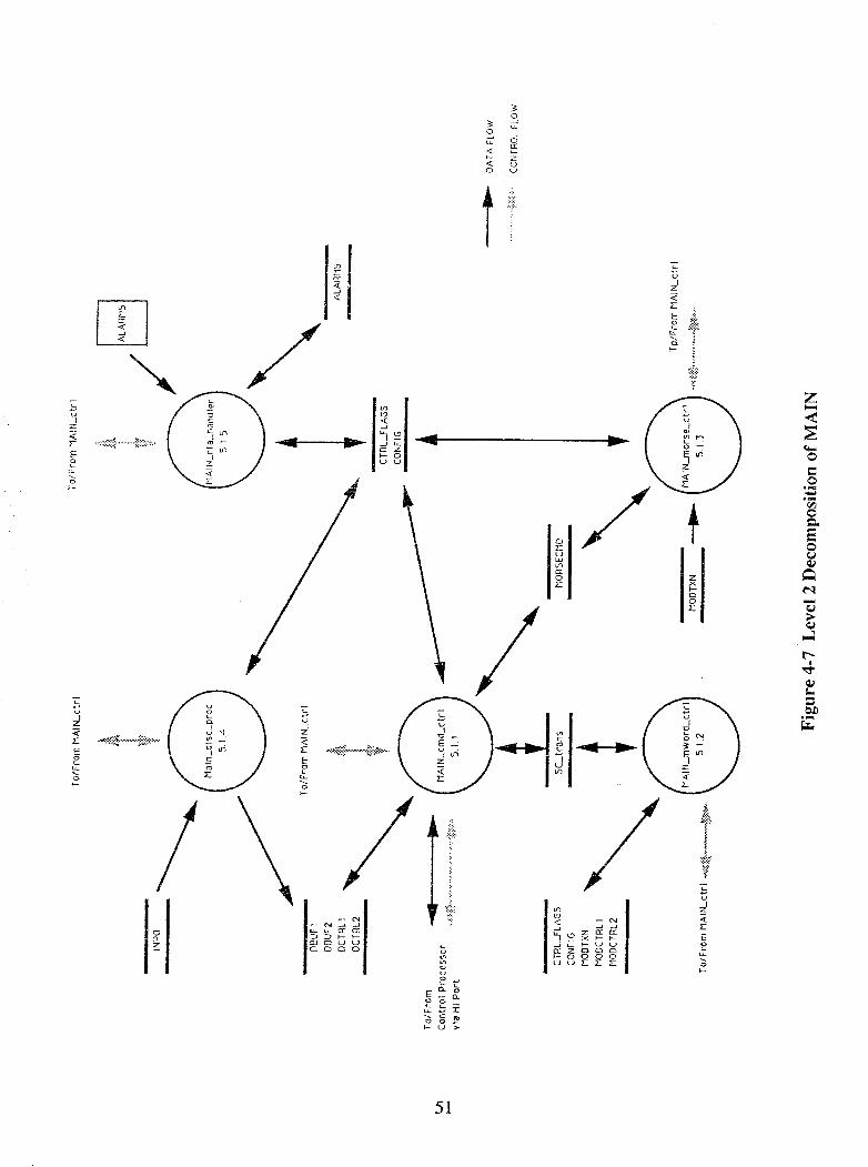
CT
RL
SL
AG
S
CO
N7 l
G
BO
OTX
N
NODC
TRL.
I
f10D
CTR
t.2
m-
CT
RL
JLA
GS
CO
NF l G
--
DA
TA
FLO
W
.,. . .
. . . , . , . .
. . , . .. ..
,. .,., .
.....
...,
.
CO
NTR
OL
FLO
W
Fig
ure
4-7
'~e
ve
l2
Dec
ompo
sitio
n of
MA
IN
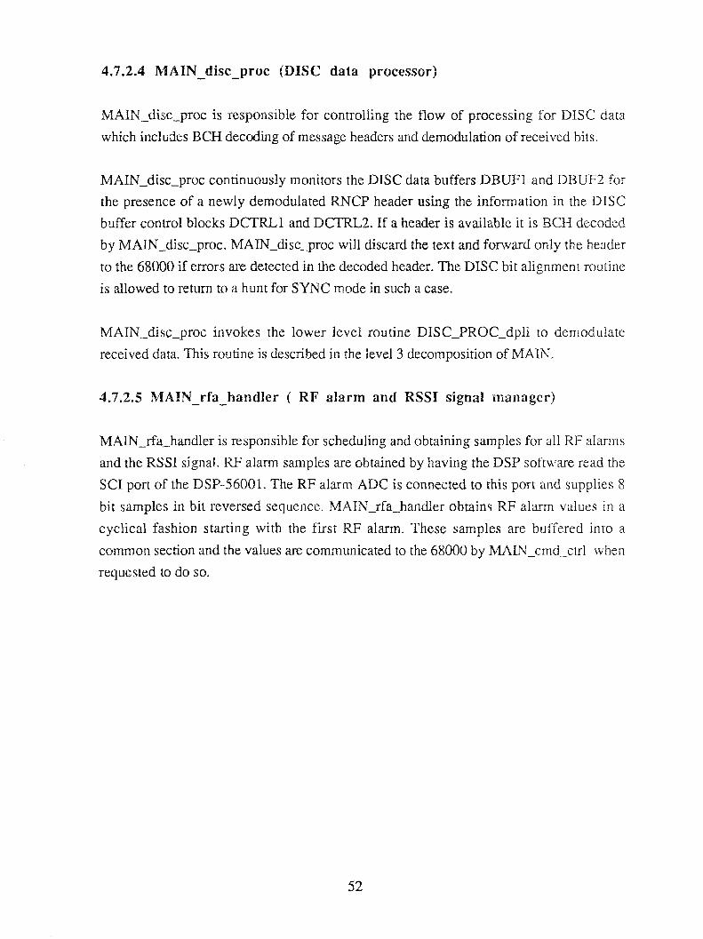
4.7.2.4 MAIN - disc - proc (DISC data processor)
MAIN-disc-mc is responsible for controi!ing the flow of processing for DTSC data
which incfndes BCH decoding of message headers and demodulation of received bits.
MAIN-disc-proc continuously monitors the DISC data buffers DBUFl and DBUF2 for
the presence of a newly demodulated RNCP header using the information in the DISC
buffer control blocks DCTRLl and DCTRL2. If a header is available it is BCH decoded
by MAINdisc-proc. MAIN_disc-proc will discard the text and forward only the header
to the 68000 if errors are detected in the decoded header. The DISC bit alignment routine
is allowed to return to a hunt for SYNC mode in such a case.
MAIN-disc-proc invokes rhe lower level routine DISC-PROC-dplf to demodulate
received data. This routine is described in the level 3 decomposition of MAIN.
4.7.2.5 1MAfN - rira - handfer ( RF alarm and RSSI signal manager)
MAIN-rFd-handler is responsible for scheduling and obtaining samples for all RF alarms
and the RSSI signal. RF alarm samples are obtained by having the DSP software rcad the
SCI port of the DSP-56001. The RF alarrri ADC is connected to this port and supplies 8
bit samples in bit reversed sequence. MAIN-rfa-handier obtains RF alarm vaiues ii; a
cyclical fashion starting with the first RF alarm. These samples are buffered into a
common section and the values are communicated to the 68000 by MAIN-cmdctrl when
requested to do so.

4.7.3 LEVEL 3 DECOMPOSITION OF MAIN
The kve1 3 deccmposi th of MAIN consists of further decomposition to the !eve1 2
routines MAIN-cmd-ctrl and MAIl4-disc-proc. The decompositions for these level 3
modules are described in sections 4.7.3.1 and 4.7.3.2 respef lively.
The data flow and control diagaii of MAIN-cmd-ctrl is shown in Figure 4-8. From this
diagram it can. be seen that XiAfN-cmd-ctrf is further decomposed into the following
lower level modules:
CMD-exec-cp-cmd (Execute 68000 comn~ands) (sec 4.7.3.1)
CiliID-send-queued-msg (Send qtleued message to the 68000) (sec 4.7.3.2)
CMD-send-disc-data (Fetch message data from DISC data buffers)(sec 4.7.3.3)
C3lD_cp_xmit (Transmi: data or commands to the 68000) (sec 4.7.3.4)
These modules are cfiscussed in the reference subsections indicated
MAIN - disc - proc (DISC data processor)
3L4I~disc-proc is responsible for coordinating the processing of DISC dsttt. This
processing involves rhe foliowi~g operations:
Detection of inbound data for asserting ch,annel multiple access protocols
Recovery of transmined data clock
* Recovery of data bits
Alignment of data bits into RNCP symbols
* Alignment of RNCP symbols inro header and text blocks
- BCH decoding of message hzaders
Figwe 4-9 shows &e -&ta :low a d conmf diagiarrt of M&ffG-&sc_prm i ~ h i ~ h carries our
the above processing. From the diagram it can be seer; that MAIN-disc-proc is
decomposed into the following secondary modules:

DISC-PRRO-dpl (Phase Iocked loop for timing recovery) (sec 4.7.3.5)
DIS C-PROC-aiign (Bit aIimment ) (see 3.7.3.6)
DISC-PROCbusy @am detection) (sec 4.7.3.7,l
DISC-PROC_bch-dez (BCH decoder for RNGP message headers) (sec 3.7.3.8 j
The lowe. level mutines of NfAm-disc-proc are discussed in the subseeti~ns indicated.
4.7.3.1 CMD - exec - el; - cmd (Execute 68000 commandsj
CMD-exec-cp-cmd serves as the gateway for ail 5801X) comnrands. CkD-exec-cp-cmd
is responsible for updating processing conditions and informatiori in response to
commands received over the HI pori. ClIILD-exec-cp-cmd ini,iates a desired 68OIXf action
directly by performing the action or indkectly by setting up the appropriate global common .. --- - areas for execution by othsr routines.
47.3.2 CMI) - send - queued - msg (Send queued DSP to 68000 messages)
CMD-send-queued-msg is responsible for transmitting messages from the
BACKLOG-MSG-Q to the 68000. The BACKLOG-MSG-Q contains messages which
previously could not be namrnitted to the 68000 due to blocking at the 68000 side of the
HT port, A message is removed from the backlog message queue if
CMD-send-queued-msg is able to transmit the queued message o:herwiss there is no
change to BACKLOG-XfSG-Q.
4.7.3.3 ChgD send disc data (Send DISC data to the 68000) - - -
CMD-send-disc-data is responsible for transferring packetized dern~dufared inbound
RXCP message data ro :he 58000. CMD-send-disc-dm will! oansmit only the header
portio:: of a received message if the message header has enors detected in it. The rransfer
of message data from a DISC dam buffer begins upon successful recep~ion of s message
header. The transfer of dam from a DISC data buffer may be preempted by the prernarure
detection of a SYR'C condition durirlg &P operation nf hii alignment (i-e. anor her SY Y C
pattern detected b t t f o ~ rhe cumnt message has been completely transfened). i n such a
case the message m s f e r in proegress will be terminated and a end of data message wili be
issued. Processing will continue with the new message.
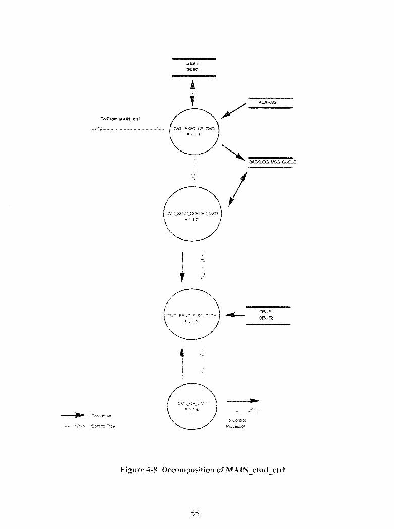

4 , 7 3 4 CMD - cp - xmit (Write data/commands ia the Hf port)
CMD-cp-xmit is respctnsible for wriiing dala or commands to the HI port using the
eransfer p r o t ~ o i s in the 68CW arrd DSP-56WT interface _rtro"otocr_ti, A message fmrn the
DSP-SSOOI to 68000 will be queued to BACKLOGcC;hISG-Q if the HI port contains
unread data when ChD-cp-xmit is ready to write the HI port, All messages inserted into
[Ire backlog message queue zrre rescheduled for rransmission at a later time.
4,7325 DISC - PROC - dpff (Phase locked h a p for timing recotery)
DlSCPROC-dpil is responsible for processing izbound DISC data arid for recovering the
received bit sequence. The demodulation algorithm used is a version of a yeif-
syncbmxizing digital phase iocked loop ivkich is described in greater dstsit in section 5-1.
The operations perfom& by the de;izdi;ia:ion algorithm include:
Data for DISC-PROcdpil is rmd frmm th t i n p t data buffer KPQ and are subsainplrd
by a factor of 2 so thaz only 8 rrts of $6 available savples we prizcsssed. (This i b done to
reduce rke processing iosd OK 'Jit DSP-S6Wl since DIf C-PROC-apfl is a critical rourxe
which Z U S i execare e%;sry bit t h e . Shuizl isn studies perfomed hake showin rhar i t i s
~ a s s i b k ;a ri=t$liii the same 12;.s! 05 demodti;!a;ion peri'crmance with onill 8 in:-read of f G
samples,). These sampies x e 13w passed Ekered with a 4th order digitai mter a d then + -
analyzed fm timine i- eno;. E ~ X S !a riming are adj jasred for by Xhmcifig or retm2ing rile
pmcesslng poiuter ro S P Q . Data decision is pesfomed using a zbxeshold cornparimn of
&e szmpk in &;re rpliddk of rhz bit windm zgzinst: fixed threshofds. Each dsc~riunsd bir is

passed by DISCPRQC-dpU to the bit aiignmenr routine DISC-PROC-align to search for
frame synchonization or data packing.
4.7.3.5 DISC - PROC - align (Align bits into words)
DISCPROG-dign is responsible for detecting the start I valid iWCP messages using
the decisioned bits from DISC-PROC-dpil. DISC-proc-align is also responsible for
aligning bits onto the correct symbol boundaries once an RNGP message boundary has
been located. Each aligned RNCP symbol is packaged into the least :&Lint 7 bits of a
byts, ?%e individual RKCP symbols are then packaged 3 per 24 bit DSP-56001 word in
prepsarion for traznsl'er ro he 68mO.
DISC-PRROC-align detecls the start of a valid PNGP message by scanning the decisioned b;' ., sq--- . ,am for the frame synchronization (SYNC) codewords of the RNCP message
protocol. DISC-PROG-align perfoms majority voting on demodulated bits before testing
for the presence of SYKC. hlzjm5ty voting mast be performed on all bits of a KNCP
header wen after SYSC has been detected in order to properly extract he message header
cmtertis, Majority voring is not required for processing the bits for the text blocks.
DISC-PROC-align PXtraCES the number of rext blocks for a message from the majority
vo;ed header. This informa$ion is used to determine the end of a message. A current
message ans sac ti or? will be aborted if a SYNC condition is detected prior to the end of a
message 2s determined by rhe text block count field in the header. In such a case
DISCPROCalign is ailowed ro return to SYXC hmt mode to start the search for ihe
next message boundary.
DiSC-PROC-busy is responsibie for perfuming data detection for tile purpose of
asening ~ h f : channl busy Sir in DSMA based multipk access prorocoi;, The algorithm
used by Elf SG-PROC-busy is described in detail in section 5-3. The algorirhm works by
sekcriveiy bandpass f i l t ehg a spec~af component at 48W Hz which is generared by
p e t f ~ ~ ~ ~ i ~ g a non-linez nwr~rinn -Y-----=- nq -= the re~ek-ed data; A comp&~n of the energy level
of ihe 4800 Hz spscnai component is compared against fixed decision thresholds ro
detz-mine whether valid d a a is presem or nor.

DISC-PROC-busy executes using the !ow pass filtered data processed by
DISC-PROC-dpll. DISC-PROC-busy performs a further daa reduction and processes
only half the data (113 the sampling rate ) that DISC-IDROC-dpll processes in order to
keep tile processing in DISC-PROC-busy at a minimum.
4.7.3.8 DISC PROC - bch - dec (BCR decoder for message header)
DISC-PROC-Schhdee is responsible for performing error detection on extracted inbound
message headers using BCH decoding 2na for determining the radio channel protocol
when the ARDPC is configured to handle both standard and extended message headers
Standard headers of the RNCP protocol family have 12 bit MID fields and 24 BCH parity
bits appended to the header while extended header has an 18 bit MID field and 18 BCH
parity bits appended. When the ARDPC is configured to handle both standard and
extended headers, an extracted header is BCH decoded twice using BCH rou~ines specific
for the standard and extended message headers. The BCH routine returning a successful
decoding is declared to be be promcol type. A header with a detected error is labelled with
a decoding failure and will be aznsferred by MAIN-ctrl to the 68000 but any rexr
associated with a failed header is discarded.

Dait f low
... .... _... ....... ................ Control Flaw ...
Figure 4-9 Decompcisition of MAIN-disc - proc

4.8 DATA DICTIONARY
ALARMS - Buffer for W a l m s and RSSI samples
BACKLOGMSG-QUEUE
- Stores 68000 response messages which initially could no; be
tfmsmit?ed to the 48000 via the HI port
CONFIG - Contains DSP-56001 configuration infomation
CTRL-FLAGS - Contains current processor state information and busy bit
information
DBUFl
DBUF2 - Buffers for demodulated and packetized DISC data
D m 1
DCTRL2 - Control bIock for DBUFl and DEW2
DEh40DDBIT - Data store for ckmodulzted bits
FLTQUE - Buffer for filtered DTSC data samples
INPQ - Buffer for rzw DISC samples
MODBUFI
TvrODBW2 - Buffers for packetized RNCP msssagcs received from he 68000
for modulation on the outbound channel
MORSEC&iCI - Common secrion used for transfer of data and conrroi beriveen
MAfl~morss-cnl and SC-morse-server

- Temporary sample queue for SC-morse-server to store i bii time
of Cara
- Buffter for modulation data samples
- Common section used to communicate between
CMD-exec-cp-cmd and MAIN-mword-ctrl 2nd
L W - m o m - c nl
- Storage for 1 bit time w r t h of modulation data samples
- Corr;mon section used far transfer of data and control between
X$ALV-mworrl_cd and SC-msg-sewer

4.9 SOFTWARE TREE
RIAIN h4l4BY-ini t
MAIN-Hl_rx
h-ULN-c trf
MAIN-c rnd-ctfl ChIDIDexecCq-cmd
CkD-send-queued-msg
CiliID-send-discdata
ChD-cp-mi$
%t4 N-m worQ ~1
h WIX-m ~rse-c irl
MAEV-disc_proc
Df 1, C-PROC-dpll -Tn-
UJ st-mut-dip
DISC-PROCbusy
DIS CPROC-kh-dec
MA IN-rfii-handler
(sec 3.7.1 2)
(sec 4.7.1.3)
(sec 4.7-1, i j
(sec 4-7.2.1)
(sec 4.7.3.1 j
(sec 4.7.3.2)
(sec 4.7.3.3)
(sec 4.7.3.4)
(ssi: 4.7.2.2)
(sec 4.7.2.3)
fsec 4.7.2.4)
(see 1.7.3.5) * - - .
(sec 4. /.J.o)
(sec 4-73?)
(sec 4.7.3.8)
fsec 4-7-25) '

This section discusses in detail the key DS? algorithms iizplemented in the ARDPC
software architecture. The algorithms described include the demodulator, modulator and
the datzl detection algorithms. The description of the demodulator algorithm provides the
details for bit timing and data recovery of received RNCP data. The discussion of the
modulator algorithn: provides details for RNCP waveform generation, while the
&scussion of the data detedon algorithm derails the technique used by the DSP-56001 to
sense the presence of inbound data over the radio chamel.
The main purpose of the ARDPC demodulator is to recover received data from a noisy
baseband signal silppiied by the base station radio discriminator, The algorithm used is an
implementation of a self-synchronizing digiral phase latked loop which executes every bit
rime as previcus'!y discussed in the scfiware afchitecture.
The block diagram for the demodulator algorithm is shown in Figure 5- 1. The following
key opemions are identif ed from the figure:
Subsampling of the sampied DISC signal
Digiraf low pass f Itering
* Digid high pass filtering
Bit Timtrg Recovery - Data Recovsrj
Tie details of these operations are provided in the remainder of secrion 5.1.
The analog DISC signal input to the ARDPC before digital conversion is low pass filtered
udng a 4 pale analog Burrei7i.imh filter wirh a cut-off frequency of 9.6 kHz. The cu{-off CL, 11,quency was chosen to pm>*ide the fiexibiiiry to accommodate future upgrades of the
ARDPC to faster data protocols. Unfortunately the choice of cut-off frequency also places
a requirement on the DSP-56Wl software to digitally low pass filter the sampled DISC
&ta to reduce out of band coise in the range of 2.4 kHz to 9.6 kHz.


The DSP-56001 samples the filtered analog DISC data at 76.8 H z , which provides 16
samples per bit for processing. The sampled data is further subsarnpfed (by a factor of 2)
by the demodulator algorithm so that only 8 of the 16 available samples per bit are actually
processed. This subsampling is performed ro halve the potential processing bandwidth
consumed by [he demodulation algorithm.
The subsampled DISC data is digitally low pass filtered to reduce out of band noise using
a fourth order elliptic Infinite Impulse Response (IIR) filter. (The filter was designed using
a cut-off frequency of 3 kHz and a sampling frequency of 38.4 kHz). An elliptic filter was
chosen because this class of ER filter provided the steepest roll-off and greatest stop-band
attenuation for a given filter order. However, the superior magnitude response
performance of the elliptic filter comes at the expense of greater non-linearity in the phase
response.
The tranfer function for the low pass elliptic IIR filter is shown in equation 5.1.
Equation 5-1 was implemented using a pair of cascaded biquadratic sections u Xi 24 bit
arithmetic. These biquadratic sections are shown in Figure 5-2a. The equations used to
irnplexent the filrer are shown in equations 5-2 through 5-5. The actual DSP-56001 code
segment =sed to implement the filter is shown i~ Table 5-1. Figure 5-2b diagrams the
register map of the DSP-56001 l~sed in implementing the filter. The code in Table 5- I can
casily be converted to be generd for an Nth order IIR filter.
The frequency and phase response of the impfemented filter is shown in Figures 5.321 and
5.37 respectively. The group delay characteristic of the filter is shown in Figure 5 3 . I t

can be seen from Figure 5.3b that with the design parameters chosen, the filter
approximates a linear phase response in the critical region 0 to 2.4 kHz . (A linear phase
response in this region is desirable to maintain constant p u p delay for the data.)
Table 5-1 DSP-56001 Assembler Code for a 4th Qrder DigitaI f iR Filter
move y:disc_gain,x I
do HTIVE-SANIPLES ,en&fil ter
move y:(r7)+n,yO
mpy yO,xl,a x: (r3)+,xO
rnac -xO,yO,a
macr -xO,y l ,a
rnac xO,y!,b
macr xO,yO,b
move bl ,a
end-cell
move a,x:(r4)+
move x:(r5)-,a
e~d-PJzx
; Gee the disc gain
; Get an input sample
; scale input sample
; x0 = a1212, yO=wl(n-2)
; xO=bf02, push wl(n) to wl(n- I )
; b=bi0*wi(n)+bil*wi(n- I)+
; Si2*wi(n-2)
; xO = a22, yO =~2(i1-2)
; a=y(nj/2
; save 2 * y(n)
; rcset r3 and r5 for the nest cycle

Figure 5-2a Demodulator Low Pass IXR Filter Biquadratic Sections
tniermeciiak Filter Coefficients Output Daia Pointer Filter States
Figtare 5-2b DSP-50001 Register Pointers for the Low Pass f fR FIlter

Frequency Response of Deifiocf LPF (Fc= 3.0 ki_iiz)
2 c r
Figure 5-32 Frequency Response of Demodulator t o w Pass f l R Filter-
Frequency f1;Hz)
Figure 5-3b Phase Response of Demodulator LOK Pass IIR Filter

Figure 5-3c Group Deie? Characteristics of Demodulator Low Pass Filter
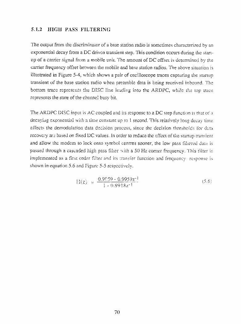

Figure 5-4 Transient Startup Candftittn of RNCP Data
Figure 5-5 Freqnenc? Response of Demodulatar High Pass Filter

5.1.3 TiMPNG RECOVERY
The block diagram for the timing recovery algorithm can be seen in boxed area of Figure
5-1. Tfie dgorithi is based on an exly-late gate dgosithrn which exploits the symmetry in
the pulses of the baseband RNCP signal to lock onto symbol centres and adjust to riming . . p e r . The input to the timing recovery aigorkhrn Is the filtered data sil.mpies generated after
low and high pass filtering. A window of 8 samples is available for use by the timing
recovery aigorithm evcy bit time.
The t h i n g recovery algorithm is based on geometric arguments and z description of :he
basic RNCP pulse replica is tisefiri in ui;derstan&ng t h t rationde behind it. A sequence of
RNCP pulses are shown ii; Figure 2-2. The wavef~rms are pseudo-ternary with 3 valid
levels at the symbol certrer iramely - i ,O and i-i. From Figure 2-2 it can be seen iha l the
basic pulse replica is sintlssldal in namre and possesses high symmecq. The demiidulator
riming recovery algorithm, when locked, establishes its dming cenne at the ctnxe of a
pu3se and calculates an imegral to the fefi (late gate) an& to the rig2-i: (park gate) of the - . dming cenne based on &e samples :&en. 1 i:~s is shown in Figure 5-6 v w h - e f ie data from
points C to D form the early gate and ~ o i a r s D to E ibm the late gate. The difference
bemeen the early and fate gate ir?,:ec~a!s - is Q when rhe pulse is symmetric and the timing
centre is correct. A timing error or non-zem differe~ce between early and !are gate integl-a!s . . results when the rrrnmg centre is ixorrecr. This timing en-ar is used io dtrermine rhe
direction and amount of t i m i ~ g adjustmenr to pe&m i;3. an a t t emp to lock onm the
received syrnbd cenoes.
- The timing &, error is $:Irered ~xirh a low pass Gher (250 Hz Brrrtenvurth) ro derive a
smoothed signaf which rtdkcts both the magnitrrde and sign of the riming exor. X phase . . kick in a direcrian to correct [he Emma .-- error is applied when [he 5frered error signal
exceeds esrabiished ~bresholds. A phase kick is implernenied by adjusting ~ h e d m pincer
ro the raw DISC data queue for";t-zrds or backv,wds by the appropriate number of d m
sampfes.
- <tares of the timing exor d t e r are zerxd whenever a phase correction is applied to prevent - s over correction due to filter delay. The action of the timing recovery filter is akin to that of
~q midog ia~egate and dump filler.
A &awbacl; of the riming recovery algorithm is that it suffers from a timing ambiguity
condition as shoivn in Figure 5-7. This f i p r e depicts a situation where a zero sariy/!ate
gate intcgzf difference is possible with rn i x o r ~ e c t timing censs. If the timing centre is "
established as showi;, &e a1gor;irhm ill be f~oled into belisving hat It has !ocked en ro
the correct timing centre. This is an undesirable condition because it will resulr in large - - - - * number of bit errors. F~fisnateiy the situation shown in Figure 3- l 1s unstable because a
p h e kick in any direction miif eventually migrate the timing centre back tc irs correct
gmsiiion, The simplest a ay ttc coftlpsnsate for this timing ambiguity condi~ion is to check
.tiit: s i p a d miigniuk of thz ettirlyfiare gate integrals when the timing enor is small. If the
ktteorais C arc litrl~e d and of rhe same sign, thm the correct timing cenm has been found. If
the integrals sire Isrg:: and of i3~pGre sign then the timing embigzit:; condition is found
a d a corsctive phase Kick mest be applied ro correct this sirnation.
Figure 5-6 EarfyiLate Gate Timing Recover?
Figure 5-5 EarfyiLate Gate Timing Ambiguity

As discussed in section 2.2.1, RNCP modulation consists of differential encoded bipolar
signalfing of low pass filtered rectangular pulses. In bipolar signalling, a zero is
represented by the zere dc level whiie 1's are represented as alternating positive and
negatiric puIses. Tne effeer of alternating positive and negative pulses to represent 1's is to
remove :he dc component in the -transmission of binary data while conserving bandwidth.
The basic RNCP waveform satisfies the first Nyquist criterion for inter-symbol ,-,
inrcrference. The side lobes of ;he puke decay a: a rate of lh3 coapxed to 1h for a sinc
pulse. The Iow pass filter used ro generare the pulse is a four& order digital elliptic filter
whose coefficiens are given in equarion 5.7 and are based on the switched capacitor filters
used Irz, the first generarim &sign.
An a1tema;ii.c szheme using a tapped ilebay line (FIR I'ilter) to generate rhe pulse directly
was impkmented in the XRDPC in an attempt to reducs the computariona'l load on the
DSP-56CIf processor dui-Ias - modulation. This technique initially required filccring a
rtctan:ufz pulse i l 6 samples widej md coflecring the response. The coefficients for the

pulse shaping FIR filter were then obtained by ~wncating and scding the pulse response
over a pe~ctff of 3T or 48 samples. 'vi'induwing of the FIR coefficients was not deemed
necessary since the filtered response was essentially finite over a period of 3T. The find
FIR coefficients are shown in Table 5-2.
Dwing modulation, the inpilt to :he FIR filter consists of a 4800 Hz impulse train whose
non-zero vaiues are + I. Computarionally speaking, a single sample for a RNCP pulse is
then obtained by adding or subtracting FIR filter coefficients separated by 16 samples. A
buffer consisgng of the ctimnt bit and the previous 2 bits is necessay for ihe computar-ion
of the current sample point since the filter is 48 samples wide. In ger?.mil, ihe FIR
algorithm for modulation required only 3 instructions per output sample (i.e. 3
muftipfications) ccrnpared to 40-t ins~rirctions for the direct filtered approach, r h u
realizing a substantid saving in processing bandwidth.
Table 5-2 h3odtrlation FIR Filter Coefficients

Frequency hzsponse of Mod LFF 23
Figure 5-8 Frequency Zespome of 4lodulato; Low Pass Filter
Figure 5-9 Zmpe~lse Response of Modulator Low Pass Fitter
7 8

5 . 3 DATA DETECTION ALGORITHhT
The data detection algorithm is used by the AW3PC to sense the presence of valid RNCP
messages over thz radio cfimnef i;"i a DUMA configuration. The ARDPC sets the busy bit
(of the RNCP proroco!) in subsequent outbound message symbols if a valid inbound
message is detected. Mobile unirs other rhan the current sender with messages to send will
sense that the busy bir is set aid will follow a random back off afgorihrn bef~re attempring
to transrr,Ir. The ARDPC \.;ill clear the busy bit- to indicate that the radio ch.anne! is free
when fhe current sender has completed its inbound message.
- 1 here are some characteristics desirable in a data detection algorithm. A d ~ t a deteciion
algorirhrn should possess a fast attack time for detecting the transition from random noise
:o data and vice-versa on the rsdio chanaei. The former condition is known as the "busy
-;tack time" rind the iaiter is known as t k "busy hang rime". The throughput for the radio
channef will be adversely affected if :he busy hang time is excessively long since the
available radio channel idle time ?>/ill e reduced (i.e. mobile units waiting with messages
to transmit will be biocked fro= doing so until the base station's data detection algorithm
can mike i h ~ ans sit ion from dasa to noise on the radio channel). The data detection * . zlgozi-irhm must also shmv stattli:ty during the pericd that a message is being msrnittsd on
the channe!. If the a!gori:l?m is ifnztabk then fdse windows of Idle channel time will be . &
opened, %%;hich will al1o.s a uamng rncbik to begin message transmission before the
c*menr s e x i e r has k e n complsted, ;bus resui59.; C in a colfisian and subsequent loss of
borh messaees. G

The data detection algorithm designed for the AiiDEC satisfies all the above requirements
and is simple in concept. The block diagram for the algorithm is shown in Figure 5-10.
The steps involved in the afgorithm are surfimxized as f o l i j . ~ ~ :
* the baseband RKCP signal is conve~ed into a rectanptar version of itself
using hysteresis threshofding.
a non-finear OF: ation i~ the form of a T/2 delay and multiply operation is applied to the
rectangilar signal with h e resuh that a strong spectral peak at the c l x k frequency is
generated at the output of the delay and multiply block.
* the delay and multiply ourput is bandpassed fikzred using a nmow digital bandpass filter
to isolate the clock fi-equsncy spectral ccmponent.
the absolute value of ;he bandpass filter oiiqxit is $Am, smoothed with a 250 Hz
Butternoah low pass find thsr; rhreshoided to determine the przszncefabsence of data.
Hysrerzsis is applied ro i k decision prcxess for debouncing purposes.
The theoretical spectrum of a bipolz ssignai 6oes not contain a discrete componenr at any
frequency. However, a strmg spxna i component at r h ~ , oansmirter clock frequency can
be generated with the applicadm af a non-iinear operation to rhe basebarid signal. \The
theory behind this result can be found be in rei'=rences 121 and [ I 11). Such rzlevanr non-
finear operations incliidz: abssi~te ;.due; squaring or delay and mzlripl;:. The effects c ~ f
these operatiam on simulated RXCP data were studied. The data sets used inclcded dara
and preamble segments and ivere generared ro be represenrativs of :,he ourpui of rhe
demodttfatian process, tvhich implies hat the ciam has been filrsred and subsampled 30 that
there zre 8 samples to a bii. The signaf to noise ratio of the data sets varied from ~ I I C
7 carresponding to a BER of I&- to essenfid'ty noise-free data.


using a Tf2 delay and multiply operation. (Beiays other than T!2 were also used b ~ t
resuited in a reduced c i ~ k frequency spectral component),
III the ARDPC, a window cf 8 samples of digitally r"iitered DISC data is available every bit
tine. %is data is genexi& b-j :he &modula~on algorithm for bit synchmnizarion and dara
recovery. I! was convenient fc havc the dara detection algorithn; execute at every bit riine
immediately after the demdutaciion algorithm, since bot'l atgoritkrns e m share the sarne \c=t
of input data sarnpks ',Led raw DISC samples which have Seen low passed filtered ;c
reduce noise and high ~ a s s e d E l m to reduce effects of DC offset ). Howeter. this
approach imposed an arlditicnal load on DISC Zata prxessing which, combined with
dernodtllation, could curtstrme more than Of)% of the processclr bandwidth at csmin
stages, This prompted an1 Investigation in reducing the mount ~f &ta processed for daia
detection,
Amther series of sirnuiations were performed using data which was further subsampied
by additional fzctor of 2 to determine ~ + e effects of further data rcducdofi. data used
EO generzte Figures 5-1 i &rough 5-14 was subjected to further srxbsampting and the sarne
non-linear operations cfrmspondhg to Figures 5-1 1 through 5-14 were reapplied and ihe
resuIts are shown in Figures 5-15 through 5-1 8. Overall, the sirnulatioils show that r h w
is very fittie degradation in the final resuits by processing 1,'8 rate data over 1/2 rate data.
An i~teresting resulr is shown in Figure 5-18 where the data was converted :o a
rectanguiar pulse train before being; operaied on using a Ti2 delay and multiply operation.
Figure 5-13 shows that all the multiples of the the 2400 Hz spectral component are
eliininated with the exceptiofi of the 4800 Hz component. This was a desireable p w p e q
because it provided geater flexibiiiry in [he design of the bandpass filter, which must be
used to emact the clock frequency component. Therefore this technique was adopted over
:he orhers to generate the clock frequency component for &he data detection a!?xithrn
Figure 5-11
Figure 5-12
83

Figure 5-13
Frequency kAzj
Figure 5-14
84
Figure 5-15
Frequency (Wzj
Figure 5-16
85
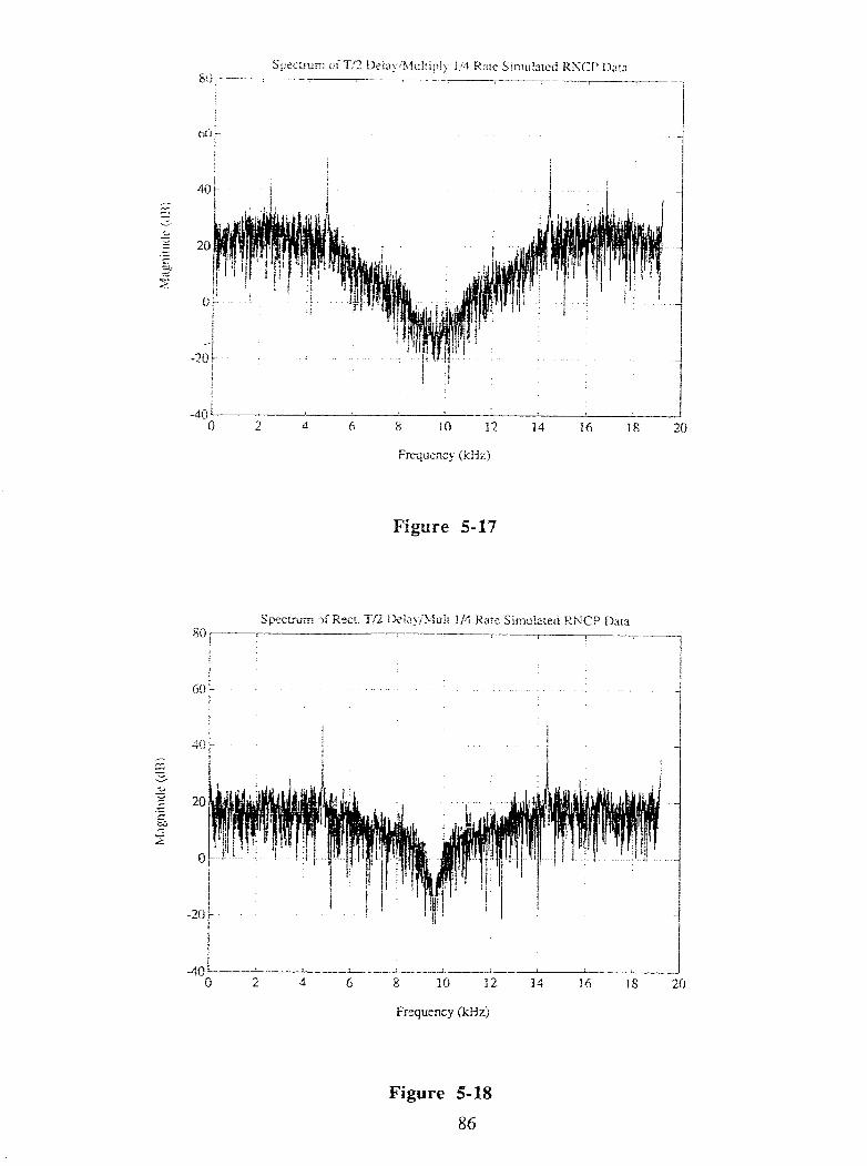
Figure 5-17
Frequency (kHz)
Figure 5-18
86

5.3.2 BANDPASS FILTERING
The spectrum of the num~t r- of the delay and mu!tiply opera~on impfan--* t. i L I I L ~ U A ---*-:-- LUJlLal i l3 a
smng discrete component at the data clock frequency (4.8 Hz). The magnitude of this
component is data dependent and is greatest when the 2.4 Mfz RNCP message preambk
is received and is we&est when a fong suing of 0's are being received. The dock
frequency spectral camponenr can be isoiated using a narrow digital banQass-filter
centred at the clock frsqt;er,cy. The bandpass filter implemented was a second order all-
pol2 filter whose poks were h a t e d on h e radial line joining the clock frequency on the
unit circle with the oiigiln;. H i g h orifsf fi!xes were attempted and produced better results,
but proved to be cornputationally expensive.
The Z uansform for thc bsridpass iilier used is given by :
Equation 5.10 reduces to the following form for 114 rrte dam:
The parameter a determines rhe width sf the f i lm passband. As with analog filters the
narrower the filter passbad (i.e. higher the Q value) the greater the delay of energy to
pass through the filter. On [he other hand increasing the filter passband width allows more
energy from adjacent frequencies to leak th-uugh resufting in a less smooth resulr.
A series of simulations were performed with different values of a. These are sho~iw in
Figure 5-19. As a increases (i.e. approaches the unit circle) it can be seen ihat the
bandpass results increase in smoothness due to gream selectivity in passing the clock
frequency component but with the drawback of greater delay in the clock frstjtiency
component achieving its maximum v a k . From the simulations it was decided :hat the best
combination of attacki&~qg rime response m d stability was for r = 0.994.

Frequency Response versus the Paraniercr "a"
F i g ~ r e 5-19 Variation of Bandpass Filter Bandwidth with Parameter 'a'

5.3.3 DATA CONDTTIONING
Three operations were used to prepare the data for decision on whether data was present
on the radio channe!. These operatio~s include the following:
rectificaGon
smootlling
geometric peak decay
The time domain ouyut of the bandpass filter include sinusoids in the neighbourhttoi; of
4800 Hz with a varying amplitude envelope. The sinusoids are strongest in the cime
domain when the 2.4 kHz RNCP rnessags preamble is presenr and varies with rhe
contents of the data streaz. It was decided to rectify this signal in order to simply ;he
decision process. This rectification was accomplished by taking the absoiute value of the
baiidpass filier oulpur.
The rectified filter oitqwt is further srnuothed with a 250 Hz Buttenwrih low pass filter to
remove rapid var;,ation in the filtered rectified octput amplitude.
The geometric decay operation is us-zd as a computationally inexpensive pe& holder to
prevent rapid variation in the filtered rectified signal when a EVCP data stream wit5 a
majority of zeroes is present. The geometric decay serves as a debouncing mechanism.
which will hold a peak level and then geometrically decay it over time when the peak le\,ei
is falling. Without the geometric peak decay, a data stream sparse in 1's: has the potential
to cause data detect faking (i-e. data misrsken for noise) by allowing the smoothed
rectified output to rapidly dzcreass in amplitude.
53.4 DECISION
The decision block in Figtre 5-10 decides on whether noise or d m is present i n the DISC
data. The decision is made by comparing the output of the conditioned signal amplitlide
against hysteresis thresholds. Hyrrercsi is used becawx an occasion, the arnp!lide of the
EilteredrectLfied result can actually dip below the noise floor even with the geometric peak
decay operation. These dropouts more or less rule out the use of single decision level,
since excessive falsing may occur, Instead a two-level hysteresis decision scheme was
implemented to debounce potential falsing which occurs when data is mistaken for noise
and viceversa. In the hysteresis decision schcrns, a data and noise floor was dstennined
using a combination of stmufation and experinents. A decision for "data present" was
made if the conditioned signal amplitude exceeded the data floor. Once "data present" was
decided, a decision for noise cnuid no: be made until the conditioned signal amplitude fell
below tile noise floor.
5.3.5 SIMULATIONS TO TEST ALGORITHM EFFECTIVENESS
A set of end to znd sirnu!stium were performed to measure the effectiveness of the data
detccdon algorithm once ail the building blocks shown in Figurc 5-10 were assembled. ' P 1 1 nree data sets distinguiskd only by the level of random noise preceding and foliowing
the RNCP preamble and data respectively were used in the tests. The data sets are shown
in Figures 5-20a thro~gh 5-20c. The normally disrributed random noise occupied sample
locations 1 through 1034 and 4046 through 5144 in all data sets. The data in locations
1025 through 3072 contaiiied i024 sampies of preamble. The RNCP data and preamble
were sixulated to be representative data for a worse case bit error rate of 10-2. The
spectrums appearing at node X in Figure 5-10 is shown in Figures 5-21a through 5-2lc.
Tfie only real difference kweer , rhe three spectral results is the magnitude of the spectrum
for frequencies gleam thm 4800 Hz.
The resulr appearing at noae 3 in Figure 5-10 is shown for d l data sets in Figures 5-21 a
rhough 5-21c. The results at node B are used to decide whether the inbound channel is
busy of not. Figcres 5-21a through 5-21c show that a noise floor threshold of 0.02 and
dam floor of 0.03 is sufficient for the data detection algorithm to have a reasonable attack
time and hang time without excessive data faking. It should be noted that there is no
definitive way to select the vafues for the hysteresis decision thresholds. The decision for
rhe value of the thresholds mist be based on the tradeoffs, which must be made between
faking and busy arm& and hang rimes. Figures 5-21 show that if rhe data floor threshold
is reduced then the busy attack dme is improved but the risk of busy falsing in increased
ready since the threshold is closer to the zvsrage value of the noise. By the same token if - the noise floor threshofid is raised then the busy hang time is improved but risk of busy
rlropout-s is increased.

Equal ioi~ibe Data , I . ? _
-(j.S ' ! 0 :i"W ?Ci 3000 a@.?> 5DKl Id kh!
Sample Nurnhr
Figure 5-20c

Spectnm of node A for L o i v Noise Data 60 i----7-
! I 1
Frequency !kHz)
Figure 52Ia
Frequency (kfizj
-" I J
O 2 6 8 I0 12 14 16 13 20
Frequency @Hz)
Figure 5-21c
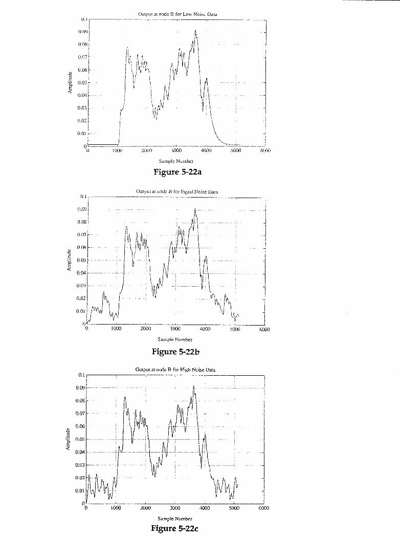
0urpt:r a: n<cdiie B for i o w hloise Data il. I --
I
Sample Number
F i p e 5-22a
Ourput a: node B for Equal h'oire Data 0. l r
i
Sample N i m k r
Figure 5-22b
Chrput ai ncdc B i ~ r High Noise Data 0.1 *
I
Sample Number
F i p e 5-22c

RESULTS
The performance of rhc ARDPC modulation, demodulation and data detection algorithms
were chzracrerized using a series of tests with a typical transmitter and receiver
combination. The emphasis was on the testing and characterization of the modem
performance and nor on the ammi rzdio used. For example the static BER sensitivity of the
modern is specified in te~ms of EbBo rather than absolure carrier level, which implies that
the tests will be repeatable using radios of different sensitivities. (Conversion from Eb/No
to zanier Iwel can be peribmed provided the noise figure and equivalent noise power
bandwidth of the radio is known.)
The demodulator performance is chardcicterized using borh static and fading BER sensitivity
r e s ~ and a bit h i n g recovery test, which measures the time to acquire tl. lock on a 3400
Hz tons. Tie modulator perilommice is characterized by measuring the specmi occupancy
and comparing the bandwidth occupied against a standard FCC spectral emission mask.
Tne data detection perfoAmance is characterized by the measurement of the busy attack and
the busy hang times. The busy attack time is the time taken from the start of an inbound
message packet to the time that the channel busy bit is actually set. The busy hang time is
~e time from the end of a message packet to the time that the channel busy bit is released.
73s processing bandwidth of the ARDPG is chmcterized by measuring the number of
instr~ctions used to perform functions.
6.1 BER SENSITIVITY TESTS
The BER ssnsiti-~ity tests characterizes the raw bit-enor performance of the modem
demodulation algorithm, The block diagram for the test is shown in Figure 6-1. Two
ARDPCs were used in the test; one to perform modulation and the other to perform
demodulation. The DSP-5E;OOi software was modified to work in conjunction with a
protocol analyzer to gznerate RXCP data representative for a pseudorandom bit strexm of
pattern length 2017 and CCITT compatible block length. The output of the modulation
AliDPC was upconverted to 800 M H i using a signal generator. The upconverted signal . . was convcrtsd to Dasebacd us i r .~ - an 800 -Vhz radio and the DISC cutput of the radio was
fed to the demodulation ARDPC. A wideband noise source was used to supply additive
white Gaussian noise. A Rayleigh fading simulator was used to simulate &ding on the
radio channel for Doppler frequency fade rates representative for vehicle speeds of 5: 20,
50 and 80 km fnr.

s -- The graphs fix rhe static ad fading BER m t s are shown ;n Pigures 6-2 2nd 6-3. The
static BER graph also includes a pior of the p d o r m a n c e of the first genn- atior; ROPC
under &e s m e test conditions. Tihis curve is provided to give a relative comparison of the
performance of the dt3rnodoIation algorithms far the first and second generation RDPCs.
From Figure 6-2 it c a t be see2 that the ARDPC with the DSP based software archiiectt~re
yields a static BER performance 2-3 dB better than the first generatictn design. The
differences in part can be attributed io the bandwidth of the low-pass filters used in the
DSP based ARDPC. (The first generation design used switched capacitor filters u i r h a
o w pass cut-off fiequexy of 5 kf!z rompx-ed :o &e PlRDPC whicl: inlp!ei;.,ented ; di&i
low-pass fiIter with a cut-off f~eqrrency of 3 kfiz)
Figure 6-1 Block Diagram for BERT Sensitivity Tests

Figure 6-2 Static BER Ferforrnance of the ARDPC
A Z D K Fadkg Performance
Figure 6-3 Fading BER Performance of the ARDPC

- 2 BIT TIMING RECOVERY
The bit timing recovery test measures the speed at which the ARBPC timing recovery
algorithm is able to adjust its symbol sampling point to the centre of the received eye
pattern. The block diagram for the test is shown in Figure 6-4.
The tests involved measuring the error in the timing recovery algorithm when receiving a
2400 Hz tone. Worst case signal to noise ratios of the tone signal were transmitted to an
800 MHz radio, whose DiSC signal was connected to the DISC line of the ARDPC. The
DSP-56001 software was modified to output the error in the timing recovery algorithm to
hardware bits, which could be monitored by a digital storage oscilloscope (DSO). The
time taken to lock (i.e. zero timing error) was determined directly from the oscilloscope
trace of tone signal and the error signal.
The results for the test is below in Table 61
Table 4-1 Bit Timing Recovery Test ResuZts
Mean time to lock @ < 10-5 static BER 4.2 msec
.,- * 90% confidence level 5.7 rnsec
Mean time to lock @ 10-2 scatic BER 5.5 msec
* 90% confidence Ievet 6.5 rnsec
These results in Table 6-1 are typically better then the first generation controlter which
averaged a mean lock time greater &an 10 msec.
Figure 6-11 Block Diagram for Bit Timing Recovery Tests
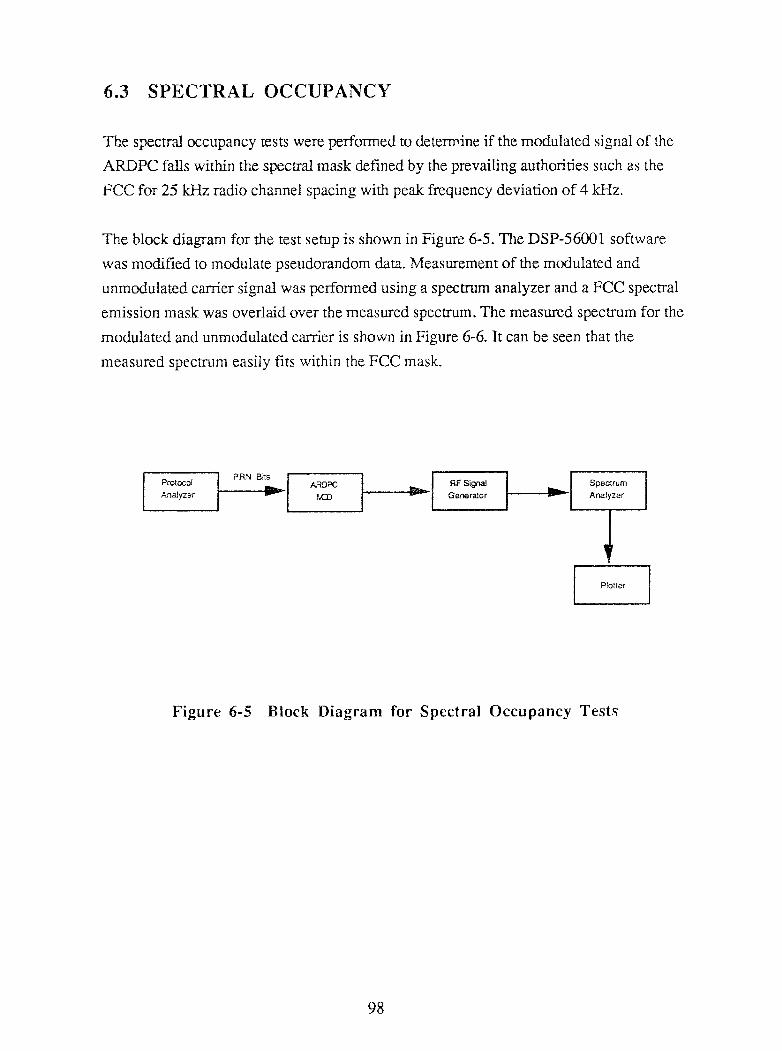
5.3 SPECTRAL OCCUPANCY
The spectral occupancy w t s were performed to determine if the modulated signal of the
ARDPC falls within the spectral mask defined by the prevailifig authorities such as the
FCC for 25 Mlz radio channel spacing with peak frequency deviation of 4 Hz.
The block diagram for the test setup is shown in Figure 6-5. The DSP-56001 softwars
was modified to modulate pseudorandom data. h4easurement of the modulated and
unrnodulated carrier signal was performed using a spectrum analyzer and a FCC spectral
emission mask was overlaid over the measured spectrum. The measured spectrum for the
modulated and unmodulaied carrier is shown in Figure 6-6. It can be seen that the
measured specirim easily fits within the FCC mask.
Analyzer Generafor
Figure 6-5 Biock Diagram for Spectral Occupancy Tests

FCC Spsct:al Enc'sston !?ask, Rug 21/90, i kHz PK Oov.
RES BU 333 Hz
1 I f SPRN 108.8 kHz . - , +$A 1la kiiz S W 3C0 msec
13.00 i(hz/Dlv
Figure 6-6 Spectral Occupancy Test Results
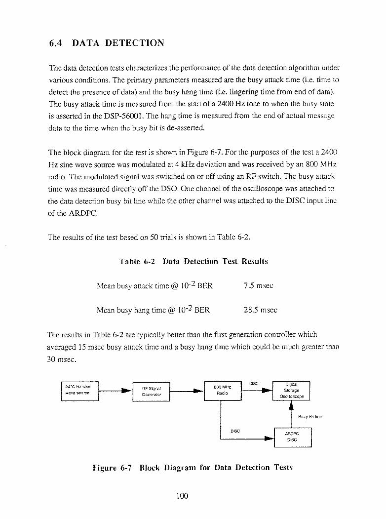
4.4 DATA DETECTION
The data detection tests characterizes the performance of the data detection algorithm under
various conditions. The primary parameters measured are the busy attack time (ix. timc to
detect h e presence of data) and the busy hang time (i.e. lingering time from end of data).
The busy artack time is measured from the start of a 2400 Hz tom to when the busy stare
is asserted in the DSP-55001. The hang time is measured from the end of acftal message
data to the time when the busy bit is de-asserted
The block diagrxn for &e test is shown in Figure 6-7. For the purposes of the test a 2400
Hz sine wave source was modulated at 4 kHz deviation and was received by an 800 MHz
radio. The modulated signai was switched on or off using an RF switch. The busy attack
time was measured directfy off the DSO. One channel of the oscilloscope was attached to
the data derection busy bit line while the other channel was attached to the DIf C input line
of the ARDPC.
The results of the test based on 50 trials is shown in Table 6-2.
Table 6-2 Data Detection Test Results
Mean busy attack time @ lom2 BER 7.5 msec
Mean busy hang time @ BER 28.5 msec
The results in Table 6-2. are rq.pica!ly better than the first generation controller which
averaged 35 msec busy attack time and a busy hang time which could be much greater than
30 met..
Figure 6-7 Block Diagram for Data Detection Tests
6-5 DSB-56001 PROCESSOR UTILIZATION
DSP-56001 processor utilization measures r'ne average number of instrmions used by the
DSP-56001 software for performing various tasks. All measurements were referewed to a
bit time. ( m e ARDPC provided a 25 MHz clock signal to the DSP-56OO!, which yielded
an 80 ns instruction time. This provided approximately 2600 instrucsions available per bit
time.) The instruction count was measured using a logic analyzer and is presented in Table
6-3.
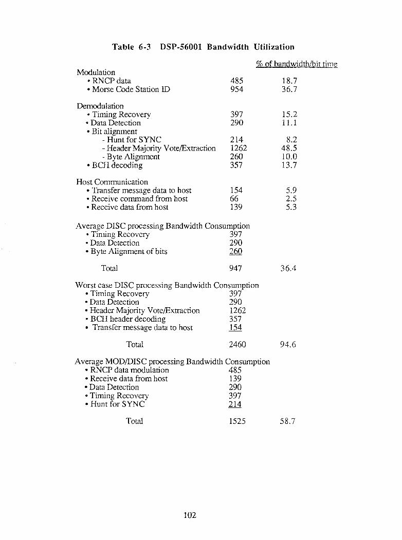
Table 6-3 DSP-56001 Bandwidth Utilizztion
% of bandwidth/bir ti1712
Modulation * RNCP data 485 18.7
Morse Code Station ID 954 36.7
Demodulation * Timing Recovery 397 15.2 - Data Detection 290 11.1
Bit alignment - Hunt for SYNC 214 8.2 - I-leader Majority VoteiExtraction 1262 48.5 - Byte Alignment 260 10.0
BCH decodi~g 357 13.7
Host Communication Transfer message data to host 154 5.9
* Receive command from host 66 2.5 Receive data from host 139 5.3
Average DISC processing Bandwidth Consumption * Timing Recovery 397 - Data Detection 290 Byte Alignment of bits 260
Total 947 36.4
case DISC processing Bandwidth Consumption Timing Recovery 397
* Data &i~ t i on 290 Header Majority VoteExnaction 1262 BCH header decoding 357 Transfer message data to host 154
Average MODDISC processing Bandwidth Consumption RNCP data modulation 485 Receive data from host 139 Data Detection 290
* Timing Recovery 397 Hunt for SYNC 214

7.0 CONCLUSIONS
Is this thesis, a DSP-56001 software requirements analysis was performed and a
proposed software achitecture alcng with accompanying DSP dgorithms was established
fcr a 4800 bps mobile data communications radio and data packet controller. The
performance of the software architecture and algorithms was proven to work successfully
through various performance tests. Overall, the performance of the DSP based modem
algorithms exceeded those of an earlier RDPC which was based on a custorr, VLSI
communications chip. The static BER performance of the DSP based controller is berter by
2-3 dB than the eslier bsc. The data detection attack and lingering times are better by up to
50% ihm the previous design.
The implemented DSP-56001 software architecture is general enough so that it can serve
as the core for any low speed duo-processor modem design. However, the archiiecture
still suffers from the constraints present in real-time applications such as processing
bandwidth, memory availability and functional requirements. A close examination of these
factors as well as a well-defined partitioning of functions is of utmost importance when
working with the DSP-56001 in particulzir and with DSP chips in general. The ftmctiona:
partitioning in a duo-processor design such as the one used for the ARDPC must take into
account the special capabilities of each processor. The DSP-56001, for example, can
perform many microprocessor control functions but it would be a waste for it to do so
since it is not optimized for the type of data manipulation that a microprocessor is capable
of. Ln the development of the ARDPC, it was a design goal to minimize the control
functions in the DSP-56001 and free i t to become an arithmetic processing engine for the
modem functions.

LIST OF REFERENCES
Tu~, William Z.Y., Mobile Commrrrricaiions Engineering, I"vfcGraw Hill
Book Company, 1982.
Spilker Jr, James J., Digital Communications by Satellite, Prentice-Hall,
1977.
Lathi, B.P., Modern Digital and Analog Communications System, Holt,
Rir!shart and Winston, 1983.
Oppenheim, Alan V. and Scahfer Ronald W., Digital Signal Processing,
-Rentice- Hall, 1875.
Handbook of Digital Signal Processing Engineering Applications,
Douglas F. Elliot ediror, Academic Press Inc., 1987.
h4ichelson Arnold M. and Levesque Allen H., Error-Control Techniques for
Digital Communications, John Wiley and Sons, 1985
Kloker, Kevin L., "The Motorola DSP56000 Digital Signal Processor", IEEE
Micro vol. 6, no. 5, pp 29-58, December 1986.
DSP 56000f56001 Digital Signal Processor User's Manual, DSP56000UhWAD
Rev 2, Motorola.
Bateman A., and Martin P.M., "A DSP-based Generic Modem for Mobile Data
Communications", Proceedmgs of Digital Signal Processing of Signals in
Communications: Loughborough, vol20-23, pp 85-87, September 1988.
Hughes, P.M., and Millar P.C., "Design of Digital Filters for Use in Frequency
Shift Keyed Modems", Proceedings of Digital Signal Processing of Signals in
Communications, Loughborough, vol22-26, pp - - 269-276, April 1985.

1 I . Gill W.J. and Spilker Jr. J.J., "An Interesting Decomposition Property for the
Self-Products of Random or Pseudorandom Binary Sequences", IEEE
Transactions on Comm:micadons Systems, pp 246-247, June 1963