a family of three-level dc-dc converters - ivo...
TRANSCRIPT
A FAMILY OF THREE-LEVEL DC-DC CONVERTERS
Antonio José Bento Bottion, Ivo BarbiFederal University of Santa Catarina - UFSC, Power Electronics Institute - INEP
PO box 5119, ZIP code 88040-970, Florianópolis, SC, [email protected], [email protected]
Abstract—This paper presents the study of a nonisolated family of dc-dc three-level converters generatedfrom a commutation cell with two diodes, two active powerswitches and one inductor. With the proposed commuta-tion cell, the basic dc-dc converter topologies, namely,Buck, Boost and Buck-Boost are obtained. Principle ofoperation, mathematical analysis, and design example areincluded in the paper, along with experimental resultstaken from a laboratory prototype rated in 500 W and50 kHz. It is demonstrated that the proposed converterfamily subjects the active power switches to lower voltage,in comparison with the conventional dc-dc non isolatedconverters, as predicted by analysis.
Keywords—Non isolated, dc-dc converters, three-level.
I. INTRODUCTION
A family of converters presented in [1] has a basic cellsimilar to that presented in this work, but the components indifferent position makes the cell in [1] unable to provide vol-tage reduction on the switch, resulting in different operationfor the respective converters.
In order to reduce the voltage switch stress of conventionaldc-dc non isolated converters many studies have been develo-ped about three-level topologies.
A study of a boost three-level topology is presented in [2].A buck three-level topology study is showed in [3].A discussion about three-level dc-dc converters employing
others topologies and modulation technics is presented in [4].This work is presented in its entirety in [5].The commutation cell proposed to reduce the voltage stress
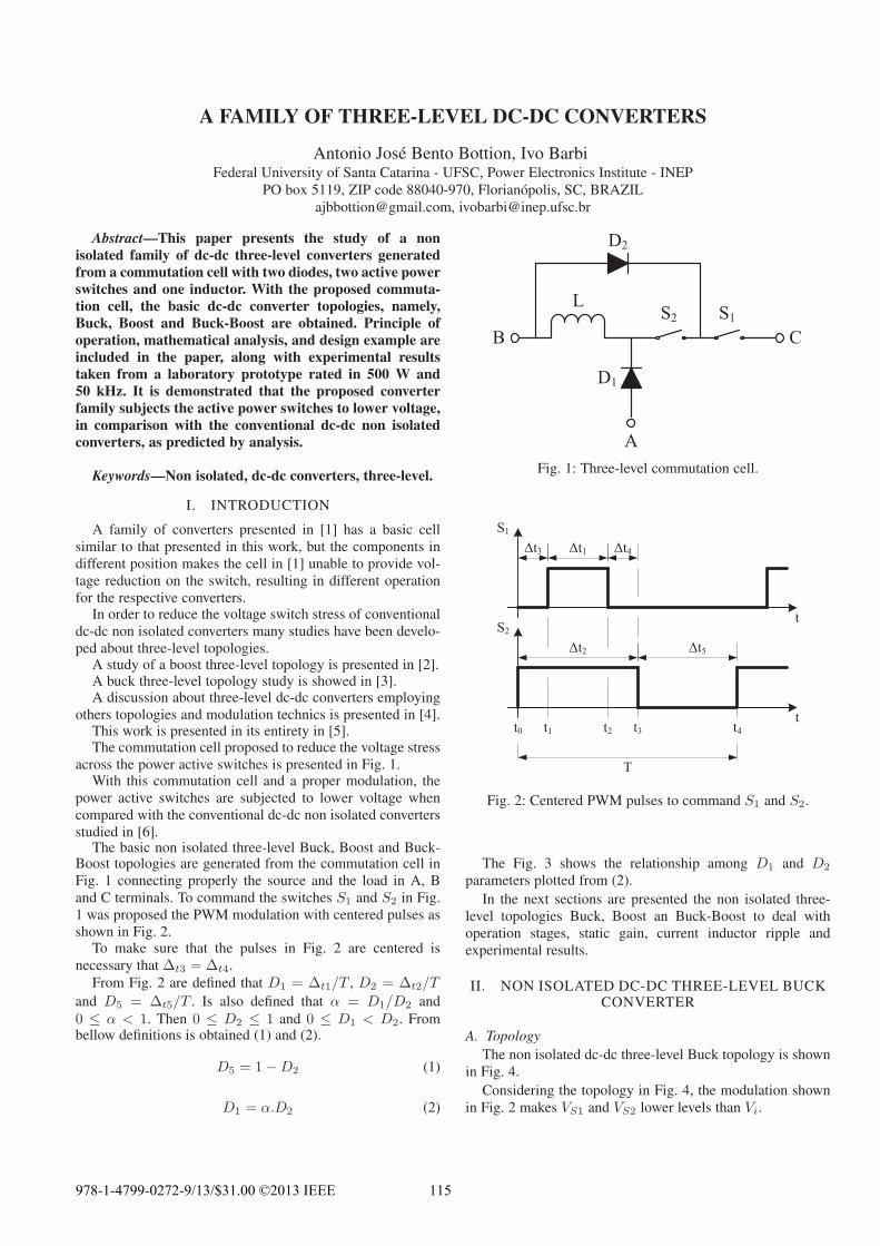
across the power active switches is presented in Fig. 1.With this commutation cell and a proper modulation, the
power active switches are subjected to lower voltage whencompared with the conventional dc-dc non isolated convertersstudied in [6].
The basic non isolated three-level Buck, Boost and Buck-Boost topologies are generated from the commutation cell inFig. 1 connecting properly the source and the load in A, Band C terminals. To command the switches S1 and S2 in Fig.1 was proposed the PWM modulation with centered pulses asshown in Fig. 2.
To make sure that the pulses in Fig. 2 are centered isnecessary that Δt3 = Δt4.
From Fig. 2 are defined that D1 = Δt1/T , D2 = Δt2/T
and D5 = Δt5/T . Is also defined that α = D1/D2 and
0 ≤ α < 1. Then 0 ≤ D2 ≤ 1 and 0 ≤ D1 < D2. Frombellow definitions is obtained (1) and (2).
D5 = 1−D2 (1)
D1 = α.D2 (2)
L
A
B C
D1
D2
S1S2
Fig. 1: Three-level commutation cell.
S1
S2
T
t
Δt1
Δt2
Δt3 Δt4
Δt5
t0 t1 t2 t3 t4t
Fig. 2: Centered PWM pulses to command S1 and S2.
The Fig. 3 shows the relationship among D1 and D2
parameters plotted from (2).
In the next sections are presented the non isolated three-level topologies Buck, Boost an Buck-Boost to deal withoperation stages, static gain, current inductor ripple andexperimental results.
II. NON ISOLATED DC-DC THREE-LEVEL BUCKCONVERTER
A. TopologyThe non isolated dc-dc three-level Buck topology is shown
in Fig. 4.
Considering the topology in Fig. 4, the modulation shownin Fig. 2 makes VS1 and VS2 lower levels than Vi.
978-1-4799-0272-9/13/$31.00 ©2013 IEEE 115

0 0.1 0.2 0.3 0.4 0.5 0.6 0.7 0.8 0.9 10
0.1
0.2
0.3
0.4
0.5
0.6
0.7
0.8
0.9
1
D2
D1
α = 0.2α = 0.4α = 0.6α = 0.8α = 1
Fig. 3: Relationship among D1 and D2 for each fixed α value.
S1 S2
D2
Vi D1
L
Vo
VS1 VS2 VL
VD1
VD2
io
iL
Fig. 4: Non isolated dc-dc three levels Buck topologyconverter.
B. Operation StagesThe non isolated dc-dc three-level Buck converter has
four operation stages considering operation in continuousconduction mode (CCM) as shown in Fig. 5.
S1
Vi D1 Vo
D2
LS2
Vi-Vo
Vo
iL
S1
Vi D1 Vo
D2
LS2
Vi-Vo
Vi
iL
S1
Vi D1 Vo
D2
LS2
Vi-Vo
Vo
iL
S1
Vi D1 Vo
D2
LS2
iL
0 V
(a) (b)
(c) (d)
Vi-Vo Vo
Fig. 5: Operation stages in continuous conduction mode(CCM).
Stage 1 [t0, t1] [Refer Fig. 5(a)]: At t0 the switch S2 isturned on and iL stay in branch L.S2.D2. The voltage acrossS1 is Vi − Vo. This stage ends when switch S1 is turned on att1.
Stage 2 [t1, t2] [Refer Fig. 5(b)]: At t1 the switch S1 is
turned on and iL increases linearly with (Vi − Vo)/L rate.
This stage ends when S1 is turned off at t2.Stage 3 [t2, t3] [Refer Fig. 5(c)]: At t2 the switch S1 is
turned off and iL stay in branch L.S2.D2 again. The voltageacross S1 is Vi − Vo like the stage 1. This stage ends whenswitch S2 is turned off at t3.
Stage 4 [t3, t4] [Refer Fig. 5(d)]: At t3 the switch S2 isturned off and both switches are off. The diode D1 conductsand iL decreases linearly with Vo/L rate. The voltage on the
switch S1 remains Vi − Vo, so the voltage at switch S2 isequal to Vo. This voltage distribution in the switches dependson its drain-source off-resistance and its intrinsic drain-sourcecapacitors. This stage ends when switch S2 is turned on at t4starting a new operation period.
C. Principal WaveformsThe principal waveforms considering operation on conti-
nuous conduction mode (CCM) are shown in Fig. 6. In thisfigure its clear that the maximum voltage across each activeswitch is always lower than input voltage, that is the highestvoltage involved in conversion.
io
tt0 t1 t2 t3 t4
IM
Im
ii
t
IM
Im
iS2
t
IM
Im
vS2
Vo
t
iS1
t
IM
Im
vS1
t
Vi-Vo
iL
t
IM
Im
Fig. 6: Principal waveforms considering operation on conti-nuous conduction mode (CCM).
116

D. Voltage static gainFrom mathematical analysis, considering operation on
continuous conduction mode (CCM), the voltage static gainis given by (3) as a function of D1 and by (4) as a function ofD2.
q =Vo
Vi=
α.D1
α.(D1 + 1)−D1(3)
q =Vo
Vi=
α.D2
1 +D2.(α− 1)(4)
The voltage static gain on discontinuous conduction mode(DCM), is given by (5) as a function of D2.
q =Vo
Vi= 1− Vo.(1−D2)
2
2.Io.L.f(5)
E. L Inductor rippleFrom theoretical analysis considering operation on con-
tinuous conduction mode (CCM) the lowest (Im) and thehighest (IM ) current levels on inductor L is given by (6) and(7) respectively.
Im =Io
D1 + 1−D2− Vo.(1−D2)
2.L.f(6)
IM =Io
D1 + 1−D2+
Vo.(1−D2)
2.L.f(7)
Where:
Io - Load current.f - Switching frequency.
F. External CharacteristicIn order to plot the three-level Buck external characteristic
the load current was parameterized as given by (8).
Io =2.Io.L.f
Vo(8)
The Fig. 7 shows three-level Buck external characteristicfor α = 1, α = 0.8, α = 0.6 and α = 0.4.
G. Experimental resultsThe specifications for a prototype project are presented in
Tab. I.
TABLE I: Buck specifications
Parameter Value UnitVi 300 V
Vo 200 V
Po 500 W
f 50 kHz
α 0.7
Fig. 8 shows the voltage waveform on switches S1 and S2.
In Fig. 9 are shown the input voltage and output voltagewaveform.
Fig. 7: Three-level Buck external characteristic.
Fig. 8: Voltage waveform on switches S1 and S2.
Fig. 9: Input voltage and output voltage waveform.
117

III. NON ISOLATED DC-DC THREE-LEVELBOOST CONVERTER
A. TopologyThe topology of non isolated dc-dc three-level Boost
converter is shown in Fig. 10.
Vi
Vo
VS1
VS2
VLVD1
VD2
io
iL
L
S1
D2
S2
D1
Fig. 10: Non isolated dc-dc three-level Boost convertertopology.
Considering the topology in Fig. 10, the modulation shownin Fig. 2 makes VS1 and VS2 lower levels than Vo.
B. Operation StagesConsidering operation on continuous conduction mode
(CCM), the non isolated dc-dc three-level Boost converterhas four operation stages as shown in Fig. 11.
Vi
Vo
iL
(a) (b)
(c) (d)
L
D2
0V
D1
S1
S2
ViVi
Vo
iL
L
D2
D1
S1
S2
Vi
Vo-Vi
Vi
Vo
iL
L
D2
D1
S1
S2
Vi
Vo-Vi
Vi
Vo
iL
L
D2
Vi
D1
S1
S2
Vo-Vi
Vo-Vi
Fig. 11: Operation stages on continuous conduction mode(CCM).
Stage 1 [t0, t1] [Refer Fig. 11(a)]: At t0 the switch S2 isturned on and iL stay in branch L.S2.D2. The voltage acrossS1 is Vi. This stage ends when switch S1 is turned on at t1.
Stage 2 [t1, t2] [Refer Fig. 11(b)]: At t1 the switch S1 is
turned on and iL increases linearly with Vi/L rate. This stage
ends when S1 is turned off at t2.Stage 3 [t2, t3] [Refer Fig. 11(c)]: At t2 the switch S1 is
turned off and iL stay in branch L.S2.D2 again. The voltage
across S1 is Vi like the stage 1. This stage ends when switchS2 is turned off at t3.
Stage 4 [t3, t4] [Refer Fig. 11(d)]: At t3 the switch S2 isturned off and both switches are off. The diode D1 conductsand iL decreases linearly with (Vo − Vi)/L rate. The voltage
on the switch S1 remains Vi, so the voltage at switch S2 isequal to Vo − Vi. This voltage distribution in the switchesdepends on its drain-source off-resistance and its intrinsicdrain-source capacitors. This stage ends when switch S2 isturned on at t4 starting a new operation period.
C. Principal WaveformsThe principal waveforms for operation in continuous
conduction mode (CCM) are shown in Fig. 12. In this figureits clear that the maximum voltage across each active switchis always lower than output voltage, that is the highest voltageinvolved in conversion.
io
tt0 t1 t2 t3 t4
IM
Im
ii
t
IM
Im
iS2
t
IM
Im
vS2
t
iS1
t
IM
Im
vS1
Vo-Vi
t
Vi
iL
t
IM
Im
Fig. 12: Principal waveforms for operation on continuousconduction mode (CCM).
D. Voltage static gainFrom mathematical analysis, considering operation on
continuous conduction mode (CCM), the voltage static gainis given by (9) as a function of D1 and by (10) as a functionof D2.
Vo
Vi=
α+D1.(α− 1)
α−D1(9)
118

Vo
Vi=
1 +D2.(α− 1)
1−D2(10)
The voltage static gain on discontinuous conduction mode(DCM), is given by (11) as a function of D1.
q =Vo
Vi= 1 +
Vi.(D1)2
2.Io.L.f(11)
E. L Inductor rippleFrom theoretical analysis, considering operation in conti-
nuous conduction mode (CCM), the lowest and the highestcurrent levels on inductor L is given by (12) and (13)respectively.
Im =Io
1−D2− Vi.D1
2.L.f(12)
IM =Io
1−D2+
Vi.D1
2.L.f(13)
F. External CharacteristicIn order to plot the three-level Boost external characteristic
the load current was parameterized as given by (14).
Io =2.Io.L.f
Vi(14)
The Fig. 13 shows three-level Boost external characteristicfor α = 1, α = 0.8, α = 0.6 and α = 0.4.
Fig. 13: Three-level Boost external characteristic.
G. Experimental resultsThe specifications for a prototype project are presented in
Tab. II.Fig. 14 shows the voltage waveform on switches S1 and
S2.In Fig. 15 are shown the input voltage and output voltage
waveform.
TABLE II: Boost specifications
Parameter Value UnitVi 300 V
Vo 500 V
Po 500 W
f 50 kHz
α 0.77
Fig. 14: Voltage waveform on switches S1 and S2.
Fig. 15: Input voltage and output voltage waveform.
IV. NON ISOLATED DC-DC THREE-LEVELBUCK-BOOST CONVERTER
A. TopologyThe topology of non isolated dc-dc three-level Buck-Boost
converter is shown in Fig. 16.
Considering the topology in Fig. 16, the modulation shownin Fig. 2 makes VS1 and VS2 lower levels than Vi + Vo.
B. Operation StagesConsidering operation on continuous conduction mode
(CCM), the non isolated dc-dc three-level Buck-Boost con-verter has four operation stages as shown in Fig. 17.
119

Vi Vo
VS1 VS2
VL
VD1
VD2
ioiL
D2
D1
L
S1 S2
Fig. 16: Non isolated dc-dc three-level Buck-Boost convertertopology.
Vi Vo
Vi VoiL
(a) (b)
(c) (d)
S2S1
LD2
D1
Vi Vo
Vi VoiL
S2S1
LD2
D1
Vi VoVi
Vi+VoiL
S2S1
LD2
D1
Vi Vo
iL
S2S1
LD2
D1
Vi Vo
0V
Fig. 17: Operation stages on continuous conduction mode(CCM).
Stage 1 [t0, t1] [Refer Fig. 17(a)]: At t0 the switch S2 isturned on and iL stay in branch L.S2.D2. The voltage acrossS1 is Vi. This stage ends when switch S1 is turned on at t1.
Stage 2 [t1, t2] [Refer Fig. 17(b)]: At t1 the switch S1 is
turned on and iL increases linearly with Vi/L rate. This stage
ends when S1 is turned off at t2.Stage 3 [t2, t3] [Refer Fig. 17(c)]: At t2 the switch S1 is
turned off and iL stay in branch L.S2.D2 again. The voltageacross S1 is Vi like the stage 1. This stage ends when switchS2 is turned off at t3.
Stage 4 [t3, t4] [Refer Fig. 17(d)]: At t3 the switch S2 isturned off and both switches are off. The diode D1 conductsand iL decreases linearly with Vo/L rate. The voltage on the
switch S1 remains Vi, so the voltage at switch S2 is equalto Vo. This voltage distribution in the switches depends onits drain-source off-resistance and its intrinsic drain-sourcecapacitors. This stage ends when switch S2 is turned on at t4starting a new operation period.
C. Principal WaveformsThe principal waveforms considering operation on conti-
nuous conduction mode (CCM) are shown in Fig. 18. In thisfigure its clear that the maximum voltage across each switchis always lower than the sum the input and output voltage.
D. Voltage static gainFrom mathematical analysis, considering operation on
continuous conduction mode (CCM), the voltage static gainis given by (15) as a function of D1 and by (16) as a functionof D2.
io
tt0 t1 t2 t3 t4
IM
Im
ii
t
IM
Im
iS2
t
IM
Im
vS2
t
iS1
t
IM
Im
vS1
t
Vi
iL
t
IM
Im
Vo
Fig. 18: Principal waveforms for operation on continuousconduction mode (CCM).
Vo
Vi=
α.D1
α−D1(15)
Vo
Vi=
α.D2
1−D2(16)
The voltage static gain on discontinuous conduction mode(DCM), is given by (17).
q =Vo
Vi= D1.
√Ro
2.L.f= α.D2.
√Ro
2.L.f(17)
E. L Inductor rippleFrom theoretical analysis, considering operation on conti-
nuous conduction mode (CCM) the lowest and the highestcurrent levels on inductor L is given by (18) and (19)respectively.
Im =Io
1−D2− Vi.D1
2.L.f(18)
IM =Io
1−D2+
Vi.D1
2.L.f(19)
120

F. External CharacteristicIn order to plot the three-level Buck-Boost external
characteristic the load resistor was parameterized as givenby (20).
Ro =
√Ro
2.L.f(20)
The Fig. 19 shows three-level Buck-Boost external charac-teristic for α = 1, α = 0.8, α = 0.6 and α = 0.4.
Fig. 19: Three-level Buck-Boost external characteristic.
G. Experimental resultsThe specifications for a prototype project are presented in
Tab. III.
TABLE III: Buck-Boost specifications
Parameter Value UnitVi 300 V
Vo 300 V
Po 500 W
f 50 kHz
α 0.8
Fig. 20 shows the voltage waveform on switches S1 andS2.
In Fig. 21 is shown the input voltage and output voltagewaveform.
V. CONCLUSION
From the theoretical and experimental studies presented inthe paper, we can draw the conclusions as follows.
1) The power semiconductor are subjected to lowervoltages, in comparison with the conventional twolevel dc-dc converters;
2) In opposition to the conventional converter, the newconverter family has two input variables, that canbe use not only to control the power transferred to
Fig. 20: Voltage waveform on switches S1 and S2.
Fig. 21: Input voltage and output voltage waveform.
the load, but also to improve static and dynamicperformance of the converters;
3) The operation and the quantitative analysis resultshave been validated in the laboratory;
4) It is the author’s opinion that the proposed converterfamily is appropriate to substitute the conventionalnon isolated dc-dc converters in applications wherethe voltages exceed the rated voltage of commercialpower switches, in low and medium power.
REFERENCES
[1] C. A. Bissochi Jr., F. R. S. Vicenzi, V. J. Farias, J. B.Vieira Jr., and L. C. Freitas, “Uma nova família deconversores eie,” in Congresso Brasileiro de Automática,2002, pp. 531–537.
[2] K. Viswanathan, R. Oruganti, and D. Srinivasan, “Anovel tri-state boost converter with fast dynamics,” IEEETransactions on Power Electronics, vol. 17, no. 5, pp.677–683, 2002.
121

[3] V. Yousefzadeh, E. Alarcon, and D. Maksimovic, “Three-level buck converter for envelope tracking applications,”IEEE Transactions on Power Electronics, vol. 21, no. 2,pp. 549–552, 2006.
[4] X. Ruan, B. Li, Q. Chen, S.-C. Tan, and C. Tse, “Fun-damental considerations of three-level dc-dc converters:Topologies, analyses, and control,” IEEE Transactions onCircuits and Systems I: Regular Papers, vol. 55, no. 11,pp. 3733–3743, 2008.
[5] A. Bottion, “Conversores cc-cc básicos não isoladosde três níveis,” Master’s thesis, Federal Universityof Santa Catarina, 2005. [Online]. Available:http://www.ivobarbi.com/PDF/dissertacoes/2005antoniobottion.pdf
[6] I. Barbi and D. C. Martins, Conversores CC-CC básicosnão isolados. Authors edition, 2000.
122