a look inside nanotechnology - infohouseinfohouse.p2ric.org/ref/32/31601.pdf · a look inside...
TRANSCRIPT

DOD Researchers
Provide
A Look Inside
Nanotechnology
Special
Issue
QUARTERLYVolume 6, Number 1
A M P T I AC is a DOD Informa tion Analys is Center Adm inis te red by the De fen se Info rma tion Sys tems Age n c y, De fen se Te chnical In fo rmation Cent er and Opera ted by I IT Re s e a rch Inst i t u te
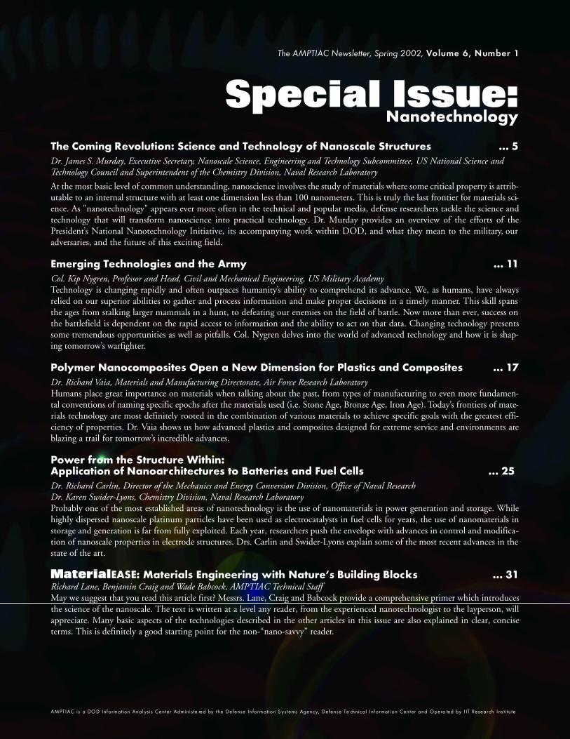
Special Issue: Nanotechnology
The Coming Revolution: Science and Technology of Nanoscale Structures … 5
Dr. James S. Murday, Executive Secretary, Nanoscale Science, Engineering and Technology Subcommittee, US National Science andTechnology Council and Superintendent of the Chemistry Division, Naval Research Laboratory
At the most basic level of common understanding, nanoscience involves the study of materials where some critical property is attrib-utable to an internal structure with at least one dimension less than 100 nanometers. This is truly the last frontier for materials sci-ence. As "nanotechnology" appears ever more often in the technical and popular media, defense researchers tackle the science andtechnology that will transform nanoscience into practical technology. Dr. Murday provides an overview of the efforts of thePresident’s National Nanotechnology Initiative, its accompanying work within DOD, and what they mean to the military, ouradversaries, and the future of this exciting field.
Emerging Technologies and the Army … 11
Col. Kip Nygren, Professor and Head, Civil and Mechanical Engineering, US Military AcademyTechnology is changing rapidly and often outpaces humanity’s ability to comprehend its advance. We, as humans, have alwaysrelied on our superior abilities to gather and process information and make proper decisions in a timely manner. This skill spansthe ages from stalking larger mammals in a hunt, to defeating our enemies on the field of battle. Now more than ever, success onthe battlefield is dependent on the rapid access to information and the ability to act on that data. Changing technology presentssome tremendous opportunities as well as pitfalls. Col. Nygren delves into the world of advanced technology and how it is shap-ing tomorrow’s warfighter.
Polymer Nanocomposites Open a New Dimension for Plastics and Composites … 17
Dr. Richard Vaia, Materials and Manufacturing Directorate, Air Force Research LaboratoryHumans place great importance on materials when talking about the past, from types of manufacturing to even more fundamen-tal conventions of naming specific epochs after the materials used (i.e. Stone Age, Bronze Age, Iron Age). Today’s frontiers of mate-rials technology are most definitely rooted in the combination of various materials to achieve specific goals with the greatest effi-ciency of properties. Dr. Vaia shows us how advanced plastics and composites designed for extreme service and environments areblazing a trail for tomorrow’s incredible advances.
Power from the Structure Within: Application of Nanoarchitectures to Batteries and Fuel Cells … 25
Dr. Richard Carlin, Director of the Mechanics and Energy Conversion Division, Office of Naval ResearchDr. Karen Swider-Lyons, Chemistry Division, Naval Research LaboratoryProbably one of the most established areas of nanotechnology is the use of nanomaterials in power generation and storage. Whilehighly dispersed nanoscale platinum particles have been used as electrocatalysts in fuel cells for years, the use of nanomaterials instorage and generation is far from fully exploited. Each year, researchers push the envelope with advances in control and modifica-tion of nanoscale properties in electrode structures. Drs. Carlin and Swider-Lyons explain some of the most recent advances in thestate of the art.
MaterialEASE: Materials Engineering with Nature’s Building Blocks … 31Richard Lane, Benjamin Craig and Wade Babcock, AMPTIAC Technical StaffMay we suggest that you read this article first? Messrs. Lane, Craig and Babcock provide a comprehensive primer which introducesthe science of the nanoscale. The text is written at a level any reader, from the experienced nanotechnologist to the layperson, willappreciate. Many basic aspects of the technologies described in the other articles in this issue are also explained in clear, conciseterms. This is definitely a good starting point for the non-“nano-savvy” reader.
The AMPTIAC Newsletter, Spring 2002, Volume 6, Number 1
A M P T I AC is a DO D Inform at ion Anal ysis C enter Adminis te red by the Defense In form at ion S ystems Age n c y, Defense Te chnical Inf ormat ion Center and Opera ted by I IT Re s e a rch Ins t i t u te

Nanoceramic Coatings Exhibit Much Higher Toughness and Wear Resistance than Conventional Coatings … 37
Dr. Lawrence Kabacoff, Materials Science and Technology Division, Office of Naval ResearchMost military and commercial applications re q u i re surface coatings which can resist wear and corrosion. Often taken for granted,these coatings can dramatically affect the standard service intervals for machinery, useful life of large components, and overall re a d i-ness of vital systems. While most ceramic coatings do wear ve ry slow l y, they usually fail from a lack of toughness and not a lack ofwear resistance. Dr. Kabacoff describes an innova t i ve processing method which utilizes traditional equipment to deposit films ofi n t e r m i xed nano- and microscale grains which stand up to we a r, but provide significant improvements in toughness and durability.
Nanoenergetics: An Emerging Technology Area of National Importance … 43
Dr. Andrzej Miziolek, Weapons and Materials Research Directorate, Army Research LaboratoryFrom the first experiments with gunpowder and fireworks to the latest ammonium nitrate and powdered aluminum high explo-sives, man has sought to unleash the force of chemical explosives in more powerful and controlled ways. Nanotechnology allowsresearchers to bridge the gap between pure chemical evaluation and microstructural analysis, and better understand the phenome-na which make energetics work. Dr. Miziolek presents a guided tour of some of the most groundbreaking work going on today inenergetics and how nanoscience is improving our understanding of one of our oldest weapons of war.
The Army Pushes the Boundaries of Sensor Performance Through Nanotechnology … 49
Drs. Paul Amirtharaj, John Little, Gary Wood, Alma Wickenden and Doran Smith, Sensors and Electron Devices Directorate, Army Research LaboratoryThe battlefield is a place where too much information is rarely a problem. Our soldiers need every bit of data that can be collect-ed and the field of available sensors and sensing systems is growing every day. An elite team of ARL researchers present some of thelatest thinking in sensor technology and describe how nanotechnology is changing the way sensors are designed, powered, deployedand utilized in the battlespace.
Fabricating the Next Generation of Electronics from Molecular Structures … 57
Dr. Christie Marrian, Microsystems Technology Office, Defense Advanced Research Projects AgencyComputers today are fabricated primarily from silicon, its oxides and nitrides, and thin films of metals, all deposited with pat-terning technologies that are quickly approaching a physical limit of resolution. What if the next paradigm of computing was basednot on the solid, electron conducting paths of silicon and metal compounds, but on molecules and the very atomic structures thatmake up our own brains? Dr. Marrian takes us to the limits of molecular-based computing with healthy doses of science-fact andpractical evaluation of components and systems that may very well be the next revolution in computing.
Engineering the Future of Nanophotonics … 63Dr. Bob Guenther, Physics Department, Duke UniversityDr. Henry Everitt, Associate Director of the Physics Division, Army Research OfficeOptical components are already established as the foundation for tomorrow’s telecommunications systems, and are quickly becom-ing de rigueur in next generation computing technology. In order for this to move from the world of science to technological appli-cation, new ways of controlling, transmitting and conveying photonic information will be developed. Drs. Guenther and Everittexamine the world of nanophotonics and show some of the systems that will transmit, generate, and indeed compute with light.
The AMPTIAC Newsletter is published quarterly by the Advanced Materials and Processes TechnologyInformation Analysis Center (AMPTIAC). AMPTIAC is a DOD sponsored Information Analysis Center,operated by IIT Research Institute and administratively managed by the Defense Information Systems Agency(DISA), Defense Technical Information Center (DTIC). The AMPTIAC Newsletter is distributed to morethan 25,000 materials professionals around the world.
Inquiries about AMPTIAC capabilities, products and services may be addressed to Dav id H. RoseDirector, A MPTIAC3 1 5 - 3 3 9 - 7 0 2 3E M A I L : a mp t i a c @ i i t ri . o rg
U R L : h t t p :/ / a mp t i a c . i i t ri . o rg
We welcome your input! To submit your related articles, photos, notices, or ideas for future issues, please contact:
AMPTIACATTN: CHRISTIAN E. GRETHLEIN, P.E.201 Mill StreetRome, New York 13440
PHON E: 315 .339 .700 9FA X: 315 .339 .710 7
E M A I L : a mp t i a c _ n e w s @ i i t ri . o rg
Editor-in-ChiefChristian E. Grethlein, P.E.
Technical Content ManagerWade Babcock
Creative Director Greg McKinneyWord and Image
Information ProcessingJudy E. TallarinoPatricia McQuinn
Inquiry ServicesDavid J. Brumbaugh
Product SalesGina Nash
Training CoordinatorChristian E. Grethlein, P.E.

Introduction
The term “Nanoscience” is appearing in the technical literatureat an increasing frequency and each reference offers its own def-inition, some of which are better than others. At the most basiclevel of common understanding, nanoscience involves materi-als where some critical property is attributable to an internalstructure with at least one dimension limited to between 1 –100 nanometers. Below that size, the disciplines of chemistryand atomic/molecular physics have already provided detailedscientific understanding. Above that size scale, the last 50 yearsof condensed matter physics and materials science have provid-ed a detailed scientific understanding of microstructures. So, insome respects, one might consider the nanoscale to be the last“size” frontier for materials science.
The interest in nanostructures extends beyond their individ-ual properties. We have learned to exploit the natural self-assembly of atoms/molecules into crystals. The directed self-assembly of nanostructures (one, two and three dimensioned)into more complex, hierarchical systems is also an important
1980 1985 1990 1995 2000
Year
Figure 3. Nanoscience
Literature Citation Counts
Dr. James S. MurdaySuperintendent, Chemistry Division, Naval Research Laboratory
Executive Secretary, National Science and Technology Council’s Subcommittee on Nanoscale Science, Engineering and Technology
Figure 1. Paleontology
of Nanostructures
The AMPTIAC Newsletter, Volume 6, Number 1 5
Empiric Epoch Surface Epoch Nano Epoch
1960 1990
Nanolayer
Nanofilaments
Nanodots
Scanning Tunnelling Microscopy/Atomic Force Microscopy
Nanolithography (x10)
Self Assembly (x10)
Nanostructure (x10)
10000
9000
8000
7000
6000
5000
4000
3000
2000
1000
0
Figure 2. Superlattice
Devices Formed through
One-Dimensional Nano-
Technology Processing
High Electron Mobility
Transistor (HEMT)
High frequency receiver/
transmitter receiver
Quantum Cascade (QC)
Laser Gas Sensor
Vertical Cavity Surface
Emitting Laser (VCSEL)
Fiberoptic data commu-
nications, optical sen-
sors, encoder, range
finderHoneywell VCSEL
NRL InAs/AlSb HEMT
Lucent Technologies
goal. Without direct self-assembly, manufacturing costs wouldseverely limit the impact of nanotechnology.
While a scientific understanding of nanostructures is incom-plete, their use in technology dates back at least two thousandyears. The Lycurgis cup, a Roman artifact pictured in the lowerleft of Figure 1, utilized nanosized gold clusters to provide dif-ferent colors depending on front or back lighting. The Romanartisans knew how to achieve the effect, but were unaware of its
nanocluster basis. In the 20th century, nanos-tructures contributed to many significant tech-nologies. Examples of these include the additionof nanosized carbon particles to rubber forimproved mechanical properties (tires), the use ofnanosized particles for catalysis in the petro-chemical industries, and the nucleation of nano-sized silver clusters during photographic filmexposure. As depicted in Figure 1, one mightassign these examples to an empiric epoch in thecontinuing evolution of nanotechnology.
Empirically-based technology, withoutg reater scientific understanding, is usually diffi-cult to extend or control. The scientific founda-tion of nanostru c t u res re c e i ved a quantuma d vance when surface science enjoyed a re n a i s-sance, starting in the 1960s. Su rface science con-strained one material dimension into thenanometer size scale. Events catalyzing that re n-aissance we re the development of new surf a c e -s e n s i t i ve analytical tools, the ready availability ofultra-high vacuum (a by - p roduct of the space
race), and the maturity of solid-state physics (surfaces re p re-senting a controlled lattice defect – termination of re p e a t i n gunit cells). The principal economic driving force was the elec-t ronics industry, but surfaces we re also re c o g n i zed to play anessential role in many “re l i a b i l i t i e s” – adhesives, corrosion pro-tection, friction, we a r, fracture, etc. From 1960 to the pre s e n t ,s u rface science has pro g ressed from “clean, flat and cold” intothin films (two or more nanoscale interfaces) and film pro c e s s-
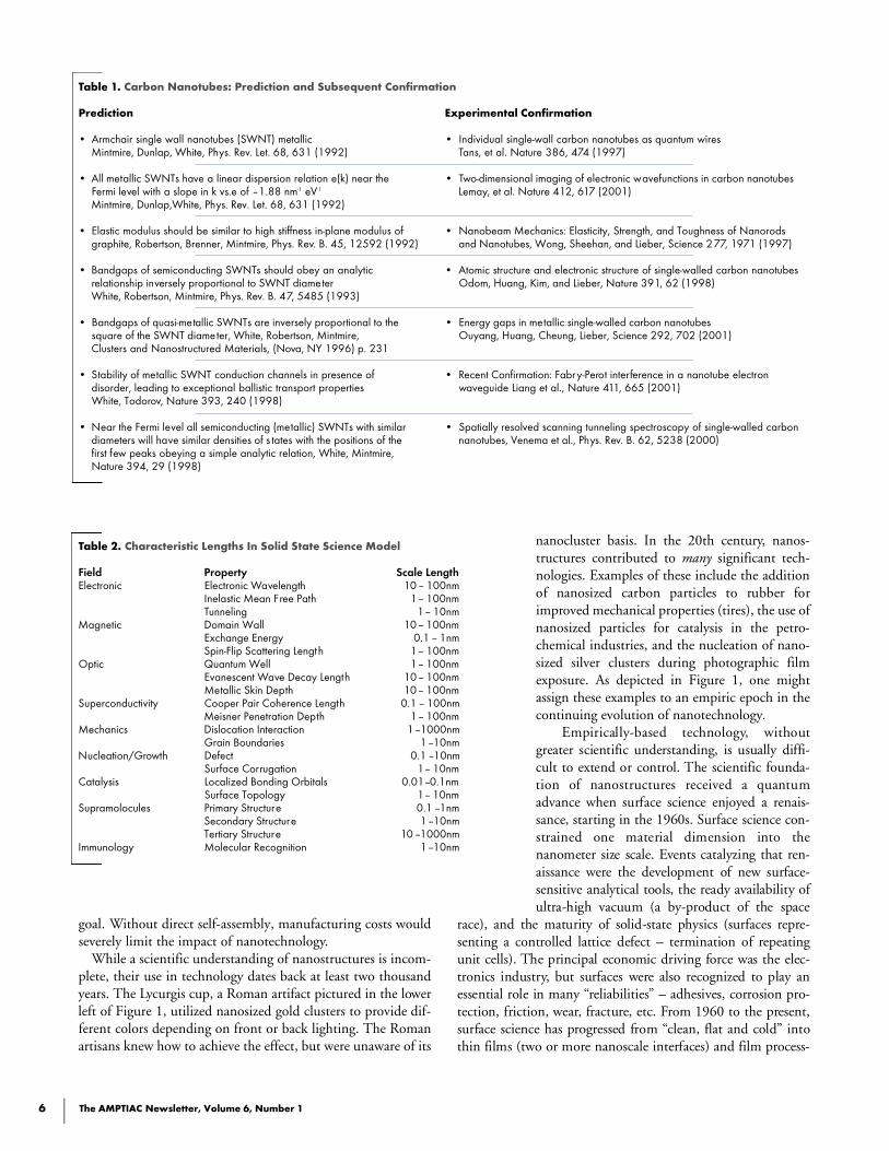
Table 2. Characteristic Lengths In Solid State Science Model
Field Property Scale Length
Electronic Electronic Wavelength 10.-- 100nm
Inelastic Mean Free Path 1.-- 100nm
Tunneling 1.-- 10nm
Magnetic Domain Wall 10.-- 100nm
Exchange Energy 0.1 -- 1nm
Spin-Flip Scattering Length 1.-- 100nm
Optic Quantum Well 1.-- 100nm
Evanescent Wave Decay Length 10.-- 100nm
Metallic Skin Depth 10.-- 100nm
Superconductivity Cooper Pair Coherence Length 0.1 -- 100nm
Meisner Penetration Depth 1.-- 100nm
Mechanics Dislocation Interaction 1.--1000nm
Grain Boundaries 1.--10nm
Nucleation/Growth Defect 0.1 --10nm
Surface Corrugation 1.-- 10nm
Catalysis Localized Bonding Orbitals 0.01 --0.1nm
Surface Topology 1.-- 10nm
Supramolocules Primary Structure 0.1 --1nm
Secondary Structure 1.--10nm
Tertiary Structure 10.--1000nm
Immunology Molecular Recognition 1.--10nm
Table 1. Carbon Nanotubes: Prediction and Subsequent Confirmation
Prediction Experimental Confirmation
• Armchair single wall nanotubes (SWNT) metallic • Individual single-wall carbon nanotubes as quantum wires
Mintmire, Dunlap, White, Phys. Rev. Let. 68, 631 (1992) Tans, et al. Nature 386, 474 (1997)
• All metallic SWNTs have a linear dispersion relation e(k) near the • Two-dimensional imaging of electronic wavefunctions in carbon nanotubes
Fermi level with a slope in k vs.e of –1.88 nm-1 eV-1 Lemay, et al. Nature 412, 617 (2001)
Mintmire, Dunlap,White, Phys. Rev. Let. 68, 631 (1992)
• Elastic modulus should be similar to high stiffness in-plane modulus of • Nanobeam Mechanics: Elasticity, Strength, and Toughness of Nanorods
graphite, Robertson, Brenner, Mintmire, Phys. Rev. B. 45, 12592 (1992) and Nanotubes, Wong, Sheehan, and Lieber, Science 277, 1971 (1997)
• Bandgaps of semiconducting SWNTs should obey an analytic • Atomic structure and electronic structure of single-walled carbon nanotubes
relationship inversely proportional to SWNT diameter Odom, Huang, Kim, and Lieber, Nature 391, 62 (1998)
White, Robertson, Mintmire, Phys. Rev. B. 47, 5485 (1993)
• Bandgaps of quasi-metallic SWNTs are inversely proportional to the • Energy gaps in metallic single-walled carbon nanotubes
square of the SWNT diameter, White, Robertson, Mintmire, Ouyang, Huang, Cheung, Lieber, Science 292, 702 (2001)
Clusters and Nanostructured Materials, (Nova, NY 1996) p. 231
• Stability of metallic SWNT conduction channels in presence of • Recent Confirmation: Fabry-Perot interference in a nanotube electron
disorder, leading to exceptional ballistic transport properties waveguide Liang et al., Nature 411, 665 (2001)
White, Todorov, Nature 393, 240 (1998)
• Near the Fermi level all semiconducting (metallic) SWNTs with similar • Spatially resolved scanning tunneling spectroscopy of single-walled carbon
diameters will have similar densities of s tates with the positions of the nanotubes, Venema et al., Phys. Rev. B. 62, 5238 (2000)
first few peaks obeying a simple analytic relation, White, Mintmire,
Nature 394, 29 (1998)
The AMPTIAC Newsletter, Volume 6, Number 16

ing. Su rface science has provided the scientific underpinningthat enabled a key aspect of “Mo o re’s Law” – the rapid minia-turization of thin film electronics technologies. Su p e r l a t t i c edevices (see Fi g u re 2) are a manifestation of the rapidly grow i n gt e c h n o l o g y, where the individual layers are nanometers in thick-ness and the interfaces are controlled with atomic pre c i s i o n .
So, if nanotechnology has been around so long, why is it onlyn ow the current rage? The 1990s nanoscience renaissance hasclose parallels to the 1960 surface science renaissance. Fi r s t ,beginning in 1980, the discove ry and development of prox i m a lp robes, such as scanning tunneling micro s c o p y / s p e c t ro s c o p y,atomic force micro s c o p y / s p e c t ro s c o p y, and near-field micro-s c o p y / s p e c t roscopy have all provided tools for measurement andmanipulation of individual nanosized stru c t u res. It took 10-15years for reliable commercial instruments to come onto the mar-ket which then led to a rapid increase in re f e reed nanosciencepublications beginning in the early 1990s. Fi g u re 3 highlightsthese increases for several subject areas. The pro p e rties of indi-vidual nanostru c t u res can now be observed, rather than re l y i n gon ensemble-averaged values. In turn, those pro p e rties can bedefined in terms of composition and/or stru c t u res, and withsuch an understanding comes the possibility for contro l .
Second, in addition to the new experimental measurementcapabilities, computer technology is now sufficiently advanced(speed and memory capacity) such that accurate predictions,even based on first principles (see AMPTIAC newsletter Vol. 5,#2, page 1), are enabled for the number of atoms incorporatedin a nanostructure (see Table 1). Analytic predictions, madeyears before experimental measurements could confirm their
validity, are now being proven true by direct experimentation.There is no doubt that modeling and simulation will play aleading role in the nanotechnology race.
Third, the disciplines of biology, chemistry, materials, andphysics have all reached a point where nanostructures are ofinterest – chemistry building up from simpler molecules,physics/materials working down from microstructures, andbiology sorting out from very complex systems into simplersubsystems. If one expected to simply extrapolate the propertiesof nanostructures from the size scales above or below, thent h e re would be little reason for the current interest innanoscience or nanotechnology.
There are three reasons why nanostructured materials behavevery differently than their adjacent scales. 1) Large surface-to-volume or interface-to-volume ratios, 2) size effects (wherecooperative phenomena like ferromagnetism are compromisedby the limited number of atoms/molecules), and 3) quantumeffects. Many of the models for materials properties at themicron and larger sizes have characteristic length scales ofnanometers (see Table 2). When the size of the structure is inthe nanometer range, those parameters are no longer adequateto model/predict the property. As such, one can expect “sur-prises,” resulting in new materials behavior that may be tech-nologically exploitable.
Finally, there are several economic engines driving the inter-est in nanotechnology, with information technology (electron-ics), biotechnology (pharmaceuticals and healthcare), andmaterials being the most likely beneficiaries (see Table 3).
With these substantial scientific and economic opportuni-ties, it’s not surprising to find strong global interest in fosteringnanoscience, with the intent of accelerating scientific discoveryinto innovative commercial products. Table 4 compares esti-mated governmental funding in nanosciences around theglobe. From estimates of FY02 budgets, it is anticipated thatover $1.5B will be invested in nanoscale science and technolo-gy (S&T) in 2002. Care should be taken when comparing
Table 3. Potential Global Economic Impact
of Nanotechnology in 15-20 Years [1]
Materials; Materials Processing $340B
Information Technology Devices $300B
Pharmaceuticals/Biotechnology $180B
Chemical Manufacturing, Catalysis $100B
Aerospace $70B
Tools, Automation, Life Cycle Costs $20B
Healthcare - Diagnostics, Prosthetics $30B
Sustainability - Agriculture, Water, Energy $45B
Total ~$1T
Table 4. “Nanotechnology” Research Program Investment ($M)
1997 2000 2001 2002
USA 115 270 420 600
Japan 120 245 500 900
Western Europe 125 200 250 300
Other Countries
(FSU, China, Australia, others) 70 110 200 400
Total 430 825 1,400 >2,200
Table 5. US National Nanotechnology Initiative Program ($M)
(Funding Breakdown)
Category Lead FY00 FY01 FY02
“Fundamental” Research 87 140 *
Grand Challenges 71 125 *
Nanostructured Materials by Design NSF
Nanoelectronics, Optoelectronics, Magnetics DOD
Advanced Healthcare/Therapeutics NIH
Environmental Improvements EPA
Energy Conversion/Storage DOE
Transportation DOT
Microcraft and Robotics NASA
Instrumentation & Metrology NIST new
Manufacturing Science NSF new
CBRE Protection/Detection DOD new
Centers/Networks 47 66 *
Infrastructure 50 77 *
Ethical/Social Implications 15 21 *
Totals (est.) 270 429 600
* Figures not available at press
The AMPTIAC Newsletter, Volume 6, Number 1 7

funding levels between different countries. For instance, oneestimate of nanotechnology investment in China is around$25M/year; however, the manpower costs in China are signifi-cantly less than in the US, therefore, their investment is not assmall as it might otherwise seem.
US National Nanotechnology Initiative
The US response to the nanoscale scientific and economicopportunities is the National Nanotechnology Initiative (NNI)[2]. The funding categories for the NNI are provided in theNational Nanotechnology In i t i a t i ve supplement to thePresident’s FY2001 Budget [3]. The annual investment levels innanoscience are presented in Table 5. It would be fair to saythat all of the S&T funded under the NNI is fundamentalresearch. On the other hand, the S&T activity designated as“fundamental” in Table 5 corresponds to NSF investmentwhere the principal motivation is the generic knowledge baseand education.
In the ‘Grand Challenges’ section of Table 5, the fundamen-tal research investments listed are selected with technologicalramifications in mind. The lead agency has the responsibilityfor surveying the investment in the designated Gr a n dChallenge and for identifying investment opportunities/short-falls. There are three new grand challenges in FY02; the last,‘C h e m i c a l / Bi o l o g i c a l / R a d i o l o g i c a l / Ex p l o s i ve (CBRE) forDetection/Protection’, seeks to enable the considerable oppor-tunities for nanostructures to impact homeland defense. Aswith any rapidly changing technology, there is some anxietyover potential economic, environmental and social disruptionby nanotechnology. In response, NSF has sponsored a work-shop to address these issues [4].
It is expected that nanoscience/nanotechnology will enablemany important advances at the boundaries between tradition-al disciplines. Interdisciplinary research must be fostered toaccelerate that expectation. Cutting edge research will alsore q u i re expensive instrumentation for measurement andmanipulation of nanostructures. The Centers/Networks and
In f r a s t ru c t u re categories aremeant to address these twopoints. Table 6 shows newCenters initiated under theNNI. The DOE Centers will be user facilities available to allscientists/engineers in a waysimilar to the DOE synchro t ro nradiation facilities.
The NNI focuses on nano-science as the enabler of nano-t e c h n o l o g y. Experience hass h own that it takes 10-20 ye a r sfor a scientific discove ry to leadto a commercial product. How-ever, among the surface science-stimulated technologies, thereare a number of products nowentering the market. T h e s eproducts are mostly the nano-
dots and nanowires that are the building blocks for systems, butthere are also composite materials. A representative listing ofthose products is shown in Table 7.
DOD Contributions to the NNI
The DOD has been investing in fundamental nanoscienceresearch for over 20 years. One of the early programs datingback to the 1980s was Ultra-submicron Electronics Research(USER). In 1997, the DOD identified several S&T topics withthe potential for significant impact on military technology.Nanoscience was selected as one of several special research area(SRA) topics. A website [5] and coordinating committee wereestablished. Its current membership is comprised of Drs.Gernot Po m renke (Air Fo rce), John Pazik (Navy), BobGuenther (Army), and Christie Marrian (DARPA). Further,each Service has a coordinating group to guide its nanoscienceprogram (see Table 8). There are many potential areas wherenanoscience/nanotechnology may significantly impact DODmissions. A selected listing is provided in Table 9.
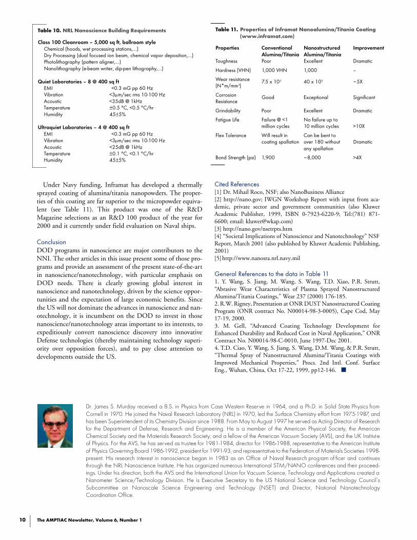
Each Service has its own laboratory nanoscience programs(see www.nanosra.nrl.navy.mil). The Army efforts in nanoelec-tronics, nanooptics, organic light emitting diodes (OLEDs)and displays, sensors, and NanoElectromechanical Systems(NEMS) are centered at ARL Adelphi; the work on organicnanomaterials is largely at ARL Aberdeen. The Air Force nano-materials program is largely centered at Wright Patterson AFBin Dayton. This work is focusing on nanocomposites, inorgan-ic nanoclusters, nanophase metals and ceramics, nanotribology,nanobiomimetics and nanoelectronics. The Navy program iscentered at the Naval Research Laboratory in Washington, DC.NRL has just created a Nanoscience Institute with the goal offostering interdisciplinary research that cuts across the NRLorganizational structures (http://nanoscience.nrl.navy.mil/). Anew Nanoscience Building at NRL has been specially designedto minimize those noise sources that would limit measurementand manipulation precision. The new building will open in2003 (see Table 10). NRL is interested in collaborative projects
Table 6. Nanotechnology Centers
Center Title Investigator Institution
National Science Foundation
Nanoscale Systems in Information Technologies Buhrman Cornell
Center for Nanoscience in Biological & Environmental Engineering Smalley Rice
Nanoscale S&E Center for Integ rated Nanopatterning & Detection Mirkin Northwestern
Center for Electronic Transport in Molecular Nanostructures Yardley Columbia
Nanoscale Systems and their Device Applications Westervelt Harvard
Center for Directed Assembly of Nanostructures Siegel RPI
DOE
Integrated NanoSystems Michalske Sandia/Los Alamos
Nanostructured Materials Lowndes Oak Ridge
Molecular Foundry Alivisatos Lawrence Berkeley
NASA
Bio/Nano/Information Technology Fusion TBD in 02
Bio-Nanotechnology Materials and Structures for Aerospace Vehicles TBD in 02
Nanoelectronics Computing and Electronics TBD in 02
DOD
Institute for Soldier Nanotechnologies TBD in 02
The AMPTIAC Newsletter, Volume 6, Number 18
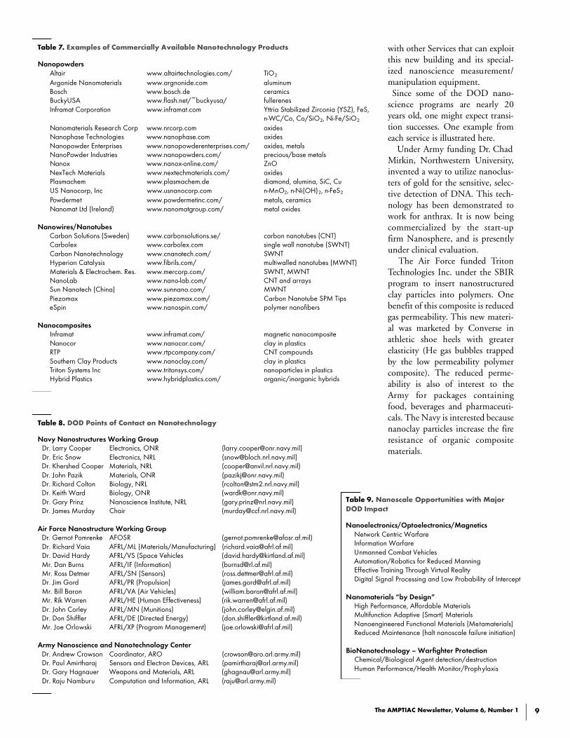
with other Services that can exploitthis new building and its special-i zed nanoscience measure m e n t /manipulation equipment.Since some of the DOD nano-
science programs are nearly 20years old, one might expect transi-tion successes. One example fro meach service is illustrated here .
Under Army funding Dr. ChadMirkin, Northwestern University,invented a way to utilize nanoclus-ters of gold for the sensitive, selec-tive detection of DNA. This tech-nology has been demonstrated towork for anthrax. It is now beingc o m m e rc i a l i zed by the start - u pfirm Nanosphere, and is presentlyunder clinical evaluation.
The Air Force funded TritonTechnologies Inc. under the SBIRprogram to insert nanostructuredclay particles into polymers. Onebenefit of this composite is reducedgas permeability. This new materi-al was marketed by Converse inathletic shoe heels with gre a t e relasticity (He gas bubbles trappedby the low permeability polymercomposite). The reduced perme-ability is also of interest to theArmy for packages containingfood, beverages and pharmaceuti-cals. The Navy is interested becausenanoclay particles increase the fireresistance of organic compositematerials.
Table 7. Examples of Commercially Available Nanotechnology Products
Nanopowders
Altair www.altairtechnologies.com/ TiO2
Argonide Nanomaterials www.argnonide.com aluminum
Bosch www.bosch.de ceramics
BuckyUSA www.flash.net/~buckyusa/ fullerenes
Inframat Corporation www.inframat.com Yttria Stabilized Zirconia (YSZ), FeS,
n-WC/Co, Co/SiO2, Ni-Fe/SiO2
Nanomaterials Research Corp www.nrcorp.com oxides
Nanophase Technologies www.nanophase.com oxides
Nanopowder Enterprises www.nanopowderenterprises.com/ oxides, metals
NanoPowder Industries www.nanopowders.com/ precious/base metals
Nanox www.nanox-online.com/ ZnO
NexTech Materials www.nextechmaterials.com/ oxides
Plasmachem www.plasmachem.de diamond, alumina, SiC, Cu
US Nanocorp, Inc www.usnanocorp.com n-MnO2, n-Ni(OH)2, n-FeS2
Powdermet www.powdermetinc.com/ metals, ceramics
Nanomat Ltd (Ireland) www.nanomatgroup.com/ metal oxides
Nanowires/Nanotubes
Carbon Solutions (Sweden) www.carbonsolutions.se/ carbon nanotubes (CNT)
Carbolex www.carbolex.com single wall nanotube (SWNT)
Carbon Nanotechnology www.cnanotech.com/ SWNT
Hyperion Catalysis www.fibrils.com/ multiwalled nanotubes (MWNT)
Materials & Electrochem. Res. www.mercorp.com/ SWNT, MWNT
NanoLab www.nano-lab.com/ CNT and arrays
Sun Nanotech (China) www.sunnano.com/ MWNT
Piezomax www.piezomax.com/ Carbon Nanotube SPM Tips
eSpin www.nanospin.com/ polymer nanofibers
Nanocomposites
Inframat www.inframat.com/ magnetic nanocomposite
Nanocor www.nanocor.com/ clay in plastics
RTP www.rtpcompany.com/ CNT compounds
Southern Clay Products www.nanoclay.com/ clay in plastics
Triton Systems Inc www.tritonsys.com/ nanoparticles in plastics
Hybrid Plastics www.hybridplastics.com/ organic/inorganic hybrids
Table 8. DOD Points of Contact on Nanotechnology
Navy Nanostructures Working Group
Dr. Larry Cooper Electronics, ONR ([email protected])
Dr. Eric Snow Electronics, NRL ([email protected])
Dr. Khershed Cooper Materials, NRL ([email protected])
Dr. John Pazik Materials, ONR ([email protected])
Dr. Richard Colton Biology, NRL ([email protected])
Dr. Keith Ward Biology, ONR ([email protected])
Dr. Gary Prinz Nanoscience Institute, NRL ([email protected])
Dr. James Murday Chair ([email protected])
Air Force Nanostructure Working Group
Dr. Gernot Pomrenke AFOSR ([email protected])
Dr. Richard Vaia AFRL/ML (Materials/Manufacturing) ([email protected])
Dr. David Hardy AFRL/VS (Space Vehicles ([email protected])
Mr. Dan Burns AFRL/IF (Information) ([email protected])
Mr. Ross Detmer AFRL/SN (Sensors) ([email protected])
Dr. Jim Gord AFRL/PR (Propulsion) ([email protected])
Mr. Bill Baron AFRL/VA (Air Vehicles) ([email protected])
Mr. Rik Warren AFRL/HE (Human Effectiveness) ([email protected])
Dr. John Corley AFRL/MN (Munitions) ([email protected])
Dr. Don Shiffler AFRL/DE (Directed Energy) ([email protected])
Mr. Joe Orlowski AFRL/XP (Program Management) ([email protected])
Army Nanoscience and Nanotechnology Center
Dr. Andrew Crowson Coordinator, ARO ([email protected])
Dr. Paul Amirtharaj Sensors and Electron Devices, ARL ([email protected])
Dr. Gary Hagnauer Weapons and Materials, ARL ([email protected])
Dr. Raju Namburu Computation and Information, ARL ([email protected])
The AMPTIAC Newsletter, Volume 6, Number 1 9
Table 9. Nanoscale Opportunities with Major
DOD Impact
Nanoelectronics/Optoelectronics/Magnetics
Network Centric Warfare
Information Warfare
Unmanned Combat Vehicles
Automation/Robotics for Reduced Manning
Effective Training Through Virtual Reality
Digital Signal Processing and Low Probability of Intercept
Nanomaterials “by Design”
High Performance, Affordable Materials
Multifunction Adaptive (Smart) Materials
Nanoengineered Functional Materials (Metamaterials)
Reduced Maintenance (halt nanoscale failure initiation)
BioNanotechnology – Warfighter Protection
Chemical/Biological Agent detection/destruction
Human Performance/Health Monitor/Prophylaxis
10
Under Navy funding, Inframat has developed a thermallysprayed coating of alumina/titania nanopowders. The proper-ties of this coating are far superior to the micropowder equiva-lent (see Table 11). This product was one of the R&DMagazine selections as an R&D 100 product of the year for2000 and it currently under field evaluation on Naval ships.
Conclusion
DOD programs in nanoscience are major contributors to theNNI. The other articles in this issue present some of those pro-grams and provide an assessment of the present state-of-the-artin nanoscience/nanotechnology, with particular emphasis onDOD needs. T h e re is clearly growing global interest innanoscience and nanotechnology, driven by the science oppor-tunities and the expectation of large economic benefits. Sincethe US will not dominate the advances in nanoscience and nan-otechnology, it is incumbent on the DOD to invest in thosenanoscience/nanotechnology areas important to its interests, toexpeditiously convert nanoscience discovery into innovativeDefense technologies (thereby maintaining technology superi-ority over opposition forces), and to pay close attention todevelopments outside the US.
Cited References
[1] Dr. Mihail Roco, NSF; also NanoBusiness Alliance[2] http://nano.gov; IWGN Workshop Report with input from aca-demic, private sector and government communities (also KluwerAcademic Publisher, 1999, ISBN 0-7923-6220-9; Tel:(781) 871-6600; email: [email protected])[3] http://nano.gov/nsetrpts.htm[4] “Societal Implications of Nanoscience and Nanotechnology” NSFReport, March 2001 (also published by Kluwer Academic Publishing,2001)[5] http://www.nanosra.nrl.navy.mil
General References to the data in Table 11
1. Y. Wang, S. Jiang, M. Wang, S. Wang, T.D. Xiao, P.R. Strutt,“Abrasive Wear Characteristics of Plasma Sprayed NanostructuredAlumina/Titania Coatings,” Wear 237 (2000) 176-185.2. R.W. Rigney, Presentation at ONR DUST Nanostructured CoatingProgram (ONR contract No. N00014-98-3-0005), Cape Cod, May17-19, 2000.3. M. Gell, “Ad vanced Coating Technology De velopment forEnhanced Durability and Reduced Cost in Naval Application,” ONRContract No. N00014-98-C-0010, June 1997-Dec 2001.4. T.D. Ciao, Y. Wang, S. Jiang, S. Wang, D.M. Wang, & P.R. Strutt,“Thermal Spray of Nanostructured Alumina/Titania Coatings withImproved Mechanical Properties,” Procs. 2nd Intl. Conf. SurfaceEng., Wuhan, China, Oct 17-22, 1999, pp12-146. ■
Dr. James S. Murday received a B.S. in Physics from Case Western Reserve in 1964, and a Ph.D. in Solid State Physics from
Cornell in 1970. He joined the Naval Research Laboratory (NRL) in 1970, led the Surface Chemistry effort from 1975-1987, and
has been Superintendent of its Chemistry Division since 1988. From May to August 1997 he served as Acting Director of Research
for the Department of Defense, Research and Engineering. He is a member of the American Physical Society, the American
Chemical Society and the Materials Research Society; and a fellow of the American Vacuum Society (AVS), and the UK Institute
of Physics. For the AVS, he has served as trustee for 1981-1984, director for 1986-1988, representative to the American Institute
of Physics Governing Board 1986-1992, president for 1991-93, and representative to the Federation of Materials Societies 1998-
present. His research interest in nanoscience began in 1983 as an Office of Naval Research program of ficer and continues
through the NRL Nanoscience Institute. He has organized numerous International STM/NANO conferences and their proceed-
ings. Under his direction, both the AVS and the International Union for Vacuum Science, Technology and Applications created a
Nanometer Science/Technology Division. He is Executive Secretary to the US National Science and Technology Council’s
S u b c o m m i t tee on Nanoscale Science Engineering and Te chnology (NSET) and Dire c to r, National Na n ote ch n o l o g y
Coordination Office.
Table 11. Properties of Inframat Nanoalumina/Titania Coating
(www.inframat.com)
Properties Conventional Nanostructured Improvement
Alumina/Titania Alumina/Titania
Toughness Poor Excellent Dramatic
Hardness (VHN) 1,000 VHN 1,000 –
Wear resistance
(N*m/mm3)7.5 x 103 40 x 103
~5X
Corrosion
ResistanceGood Exceptional Significant
Grindability Poor Excellent Dramatic
Fatigue Life Failure @ <1 No failure up to
million cycles 10 million cycles >10X
Flex Tolerance Will result in Can be bent to
coating spallation over 180 without Dramatic
any spallation
Bond Strength (psi) 1,900 ~8,000 >4X
Table 10. NRL Nanoscience Building Requirements
Class 100 Cleanroom – 5,000 sq ft, ballroom style
Chemical (hoods, wet processing stations,…)
Dry Processing (dual focused ion beam, chemical vapor deposition,…)
Photolithography (pattern aligner,…)
Nanolithography (e-beam writer, dip-pen lithography,…)
Quiet Laboratories – 8 @ 400 sq ft
EMI <0.3 mG pp 60 Hz
Vibration <3µm/sec rms 10-100 Hz
Acoustic <35dB @ 1kHz
Temperature ±0.5 °C, <0.5 °C/hr
Humidity 45±5%
Ultraquiet Laboratories – 4 @ 400 sq ft
EMI <0.3 mG pp 60 Hz
Vibration <3µm/sec rms 10-100 Hz
Acoustic <25dB @ 1kHz
Temperature ±0.1 °C, <0.1 °C/hr
Humidity 45±5%
The AMPTIAC Newsletter, Volume 6, Number 1

The AMPTIAC Newsletter, Volume 6, Number 1 67
AMPTIAC Directory
G ove rnment Pe rs o n n e l IITRI Pe rs o n n e l
TE CH N I CA L MA NAG E R/ COT R
Dr. Lewis E. Sloter IIStaff Specialist, Materials & StructuresODUSD(S&T)/Weapons Systems1777 North Kent St., Suite 9030Arlington, VA 22209-2110(703) 588-7418, Fax: (703) 588-7560Email: [email protected]
AS S O C I AT E COT RS
CERAMICS, CERAMIC COMPOSITES
Dr. S. Carlos SandayNaval Research Laboratory4555 Overlook Ave., S.W. Code 6303Washington, DC 20375-5343(202) 767-2264, Fax: (202) 404-8009Email: [email protected]
ORGANIC STRUCTURAL MATERIALS &ORGANIC MATRIX COMPOSITES
Roger GriswoldDivision ChiefUS Air ForceAFRL/MLS2179 Twelfth St., Bldg. 652Wright-Patterson AFB, OH 45433-7702(937) 656-6052, Fax: (937) 255-2945Email: [email protected]
METALS, METAL MATRIX COMPOSITES
Dr. Joe WellsArmy Research LaboratoryWeapons & Materials Research DirectorateAMSRL-WM-MCAPG, MD 21005-5069(410) 306-0752, Fax: (410) 306-0736Email: [email protected]
ELECTRONICS, ELECTRO-OPTICS, PHOTONICS
Robert L. DenisonAFRL/MLPO, Bldg. 6513005 P Street, STE 6Wright-Patterson AFB, OH 45433-7707(937) 255-4474 x3250, Fax: (937) 255-4913Email: [email protected]
ENVIRONMENTAL PROTECTION
& SPECIAL FUNCTION MATERIALS
Dr. James MurdayNaval Research Laboratory4555 Overlook Ave., S.W. Code 6100Washington, DC 20375-5320(202) 767-3026, Fax: (202) 404-7139Email: [email protected]
DEFENSE TECHNICAL INFORMATION CENTER
(DTIC) POCMelinda Rozga, DTIC-AI8725 John J. Kingman Road, STE 0944Ft. Belvoir, VA 22060-6218(703) 767-9120, Fax: (703) 767-9119Email: [email protected]
DI R E C TO R, AMPTIAC
David Rose201 Mill StreetRome, NY 13440-6916(315) 339-7023, Fax: (315) 339-7107Email: [email protected]
DE P U TY DI R E C TO R, AMPTIAC
Christian E. Grethlein, P.E.201 Mill StreetRome, NY 13440-6916(315)-339-7009, Fax: (315) 339-7107Email: [email protected]
TE CH N I CA L DI R E C TO R S
METALS, ALLOYS, METAL MATRIX
COMPOSITES (ACTING)Jeffrey Guthrie201 Mill StreetRome, NY 13440(315) 339-7058, Fax: (315) 339-7107Email: [email protected]
CERAMICS, CERAMIC COMPOSITES
Dr. Lynn Neergaard215 Wynn Drive, Suite 101Huntsville, AL 35805(256) 382-4773, Fax: (256) 382-4701Email: [email protected]
ORGANIC STRUCTURAL MATERIALS &ORGANIC MATRIX COMPOSITES
Jeffrey Guthrie201 Mill StreetRome, NY 13440(315) 339-7058, Fax: (315) 339-7107Email: [email protected]
ELECTRONICS, ELECTRO-OPTICS,PHOTONICS
Kent Kogler3146 Presidential DriveFairborn, OH 45324(937) 431-9322, Fax: (937) 431-9325Email: [email protected]
ENVIRONMENTAL PROTECTION
& SPECIAL FUNCTION MATERIALS (ACTING)Bruce E. SchulteIIT Research Institute2251 San Diego Ave., Suite A218San Diego, CA 92110-2926(619) 260-6080, Fax: (619) 260-6084Email: [email protected]
AMPTIAC Needs Your Help to Keep Our Mailing List Current!
The AMPTIAC Newsletter is currently mailed free of charge to about
25,000 subscribers. It is our policy to provide this free subscription to
anyone who would like to receive it, but we would also prefer not to send
copies to people who have no use for, or interest in, our publication.
Maintaining a current list of subscribers for a free publication is a daunt-
ing task – since we do not charge for a subscription, we have no direct
avenue for feedback from our subscribers. This is where you come in – to
keep our mailing list current, we need your help. If any of the following
situations apply, we’d like to hear from you:
• If you are reading a borrowed copy and would like your own free subscription, please ask us for one.
• If you receive the newsletter and have no use for it, please ask us toremove your name from our list of subscribers.
• If you are getting a copy under the wrong name or wrong address,please provide us with a correction.
• If you see that copies of the AMPTIAC newsletter are arriving for persons no longer working in your organization, please let us know,so we may update or delete them from our list.
We greatly appreciate your help in keeping our records current. Your
updates allow us to continue providing our readership with the best
possible source of valuable materials news and information. Additions,
deletions and corrections may be sent by email to [email protected],
telephoned to (315) 339-7092, faxed to (315) 339-7107, or mailed to
AMPTIAC, 201 Mill St., Rome, NY 13440-6916. ■