a microchip pic10-series compatible ip core design and ... · 3.2.15. pic10_alu ... into the...
TRANSCRIPT
Professional Windows Systems Programming
A Microchip PIC-Compatible RISC CPU IP Core Design and Verilog Implementation. 1
26895 Aliso Creek Rd. Suite B504 Aliso Viejo, CA 92656-5301 Phone: (877) 839-2543, Fax: (877) 349-1818 E-mail [email protected] Web http://www.SummitSoftConsulting.com
A Microchip PIC-Compatible RISC CPU IP Core Design and Verilog Implementation.

Professional Windows Systems Programming
A Microchip PIC-Compatible RISC CPU IP Core Design and Verilog Implementation. 2
26895 Aliso Creek Rd. Suite B504 Aliso Viejo, CA 92656-5301 Phone: (877) 839-2543, Fax: (877) 349-1818 E-mail [email protected] Web http://www.SummitSoftConsulting.com
Document Revision Information
Date - Version Author Comment 4/7/2007 – Version 1 By John Gulbrandsen, Summit Soft Consulting
[email protected] Initial version.

Professional Windows Systems Programming
A Microchip PIC-Compatible RISC CPU IP Core Design and Verilog Implementation. 3
26895 Aliso Creek Rd. Suite B504 Aliso Viejo, CA 92656-5301 Phone: (877) 839-2543, Fax: (877) 349-1818 E-mail [email protected] Web http://www.SummitSoftConsulting.com
Table of Contents
1. INTRODUCTION.................................................................................................................................. 6 1.1. PROJECT BACKGROUND .................................................................................................................. 6 1.2. HARDWARE AND SOFTWARE COMPATIBILITY ................................................................................. 6
2. CPU ARCHITECTURE......................................................................................................................... 8 2.1. CPU ARCHITECTURE OVERVIEW .................................................................................................... 8 2.2. DATAPATH ARCHITECTURE............................................................................................................. 9
2.2.1. Instruction Fetching ............................................................................................................... 9 2.2.2. Reset Sequence ..................................................................................................................... 11 2.2.3. Minimal Datapath required to execute simple Instructions.................................................. 12 2.2.4. The PIC10 Datapath Architecture........................................................................................ 14 2.2.5. ALU Datapath (pic10_alu_datapath)................................................................................... 17 2.2.6. Special Function Register Datapath (pic10_sfr_datapath) .................................................. 17 2.2.7. Program Counter Datapath (pic10_pc_datapath) ............................................................... 19 2.2.8. Status Register module (pic10_status_reg) .......................................................................... 22 2.2.9. Tri-State GPIO Port module (pic10_tri_state_port) ............................................................ 22 2.2.10. SFR Data Multiplexer module (pic10_sfr_data_mux).......................................................... 24 2.2.11. Program Bus Multiplexer module (pic10_program_mux).................................................... 24
2.3. CONTROLLER ARCHITECTURE....................................................................................................... 26 2.3.1. ADDWF ................................................................................................................................ 27 2.3.2. ANDWF ................................................................................................................................ 28 2.3.3. CLRF .................................................................................................................................... 29 2.3.4. CLRW ................................................................................................................................... 30 2.3.5. COMF................................................................................................................................... 31 2.3.6. DECF.................................................................................................................................... 32 2.3.7. DECFSZ ............................................................................................................................... 33 2.3.8. INCF..................................................................................................................................... 34 2.3.9. INCFSZ................................................................................................................................. 35 2.3.10. IORWF.................................................................................................................................. 36 2.3.11. MOVF................................................................................................................................... 37 2.3.12. MOVWF................................................................................................................................ 38 2.3.13. NOP ...................................................................................................................................... 39 2.3.14. RLF....................................................................................................................................... 40 2.3.15. RRF....................................................................................................................................... 41 2.3.16. SUBWF ................................................................................................................................. 42 2.3.17. SWAPF ................................................................................................................................. 43 2.3.18. XORWF................................................................................................................................. 44 2.3.19. BCF....................................................................................................................................... 45 2.3.20. BSF ....................................................................................................................................... 46 2.3.21. BTFSC .................................................................................................................................. 47 2.3.22. BTFSS................................................................................................................................... 48 2.3.23. ANDLW................................................................................................................................. 49 2.3.24. CALL..................................................................................................................................... 50 2.3.25. CLRWDT .............................................................................................................................. 51 2.3.26. GOTO ................................................................................................................................... 51 2.3.27. IORLW.................................................................................................................................. 52 2.3.28. MOVLW................................................................................................................................ 53 2.3.29. OPTION................................................................................................................................ 53 2.3.30. RETLW ................................................................................................................................. 54

Professional Windows Systems Programming
A Microchip PIC-Compatible RISC CPU IP Core Design and Verilog Implementation. 4
26895 Aliso Creek Rd. Suite B504 Aliso Viejo, CA 92656-5301 Phone: (877) 839-2543, Fax: (877) 349-1818 E-mail [email protected] Web http://www.SummitSoftConsulting.com
2.3.31. SLEEP................................................................................................................................... 55 2.3.32. TRIS ...................................................................................................................................... 55 2.3.33. XORLW................................................................................................................................. 56
3. APPENDIX A: VERILOG SOURCE CODE - PIC10 IP CORE........................................................ 57 3.1. TOP-LEVEL CPU VERILOG MODULES (CPU.V)............................................................................... 57 U
3.1.1. pic10_cpu ............................................................................................................................. 57 3.2. DATAPATH VERILOG MODULES (DATAPATH.V) ............................................................................ 61
3.2.1. pic10_datapath ..................................................................................................................... 61 3.2.2. pic10_alu_datapath .............................................................................................................. 68 3.2.3. pic10_sfr_datapath............................................................................................................... 69 3.2.4. pic10_pc_datapath ............................................................................................................... 71 3.2.5. pic10_stack ........................................................................................................................... 72 3.2.6. pic10_pc_mux....................................................................................................................... 73 3.2.7. pic10_pc ............................................................................................................................... 74 3.2.8. pic10_ir................................................................................................................................. 74 3.2.9. pic10_fsr ............................................................................................................................... 75 3.2.10. pic10_status_reg................................................................................................................... 75 3.2.11. pic10_sfr_data_mux ............................................................................................................. 76 3.2.12. pic10_register_address_mux................................................................................................ 77 3.2.13. pic10_ram_registers ............................................................................................................. 77 3.2.14. pic10_alu_mux...................................................................................................................... 78 3.2.15. pic10_alu .............................................................................................................................. 79 3.2.16. pic10_w_reg ......................................................................................................................... 89 3.2.17. pic10_tri_state_port ............................................................................................................. 90 3.2.18. pic10_program_mux............................................................................................................. 91
3.3. CONTROLLER VERILOG MODULES (CONTROLLER.V)..................................................................... 91 3.3.1. pic10_controller ................................................................................................................... 91
3.4. PROGRAM STORE VERILOG MODULES (PROGRAM_STORE.V) ...................................................... 106 3.4.1. pic10_program_store ......................................................................................................... 106
4. APPENDIX B: VERILOG SOURCE CODE - TEST BENCHES.................................................... 115 4.1. CPU_TESTBENCH.V ...................................................................................................................... 115 U
4.1.1. test_pic10_cpu .................................................................................................................... 115 4.2. DATAPATH_TESTBENCHES.V........................................................................................................ 116
4.2.1. test_pic10_tri_state_port.................................................................................................... 116 4.2.2. test_pic10_w_reg................................................................................................................ 117 4.2.3. test_pic10_alu_mux ............................................................................................................ 118 4.2.4. test_pic10_ram_registers ................................................................................................... 119 4.2.5. test_pic10_register_address_mux ...................................................................................... 120 4.2.6. test_pic10_sfr_data_mux.................................................................................................... 121 4.2.7. test_pic10_status_reg ......................................................................................................... 122 4.2.8. test_pic10_alu..................................................................................................................... 123 4.2.9. test_pic10_fsr...................................................................................................................... 134 4.2.10. test_pic10_ir ....................................................................................................................... 135 4.2.11. test_pic10_pc...................................................................................................................... 136 4.2.12. test_pic10_pc_mux ............................................................................................................. 137 4.2.13. test_pic10_stack.................................................................................................................. 137 4.2.14. test_pic10_pc_datapath...................................................................................................... 139 4.2.15. test_pic10_sfr_datapath ..................................................................................................... 141 4.2.16. test_pic10_alu_datapath..................................................................................................... 143 4.2.17. test_pic10_datapath............................................................................................................ 146

Professional Windows Systems Programming
A Microchip PIC-Compatible RISC CPU IP Core Design and Verilog Implementation. 5
26895 Aliso Creek Rd. Suite B504 Aliso Viejo, CA 92656-5301 Phone: (877) 839-2543, Fax: (877) 349-1818 E-mail [email protected] Web http://www.SummitSoftConsulting.com
Table of Figures
FIGURE 1. THE PIC10 CPU IP CORE CONTAINS THE DATAPATH AND CONTROLLER WHILE THE PROGRAM
STORE IS LOCATED OUTSIDE THE CPU CORE........................................................................................... 9 FIGURE 2. THE PROGRAM WORD FETCH LOGIC. ............................................................................................ 10 FIGURE 3. THE PIC10 CPU IP CORE STARTS EXECUTING CODE AS SOON AS THE ‘RESET’ SIGNAL IS DE-
ASSERTED.............................................................................................................................................. 11 FIGURE 4. A SIMPLIFIED DATA PATH REQUIRED FOR THE IMPLEMENTATION OF THE ADDWF INSTRUCTION.
.............................................................................................................................................................. 12 FIGURE 5. THE HIGHEST-LEVEL VERILOG MODULES INSIDE THE PIC10_DATAPATH MODULE. ....................... 14 FIGURE 6. THE CONTENTS OF THE ‘PIC10_ALU_DATAPATH’ MODULE. THE MODULE CONTAINS A DATAPATH
THAT FEEDS OPERANDS TO THE ALU AND THAT OUTPUTS THE RESULT AND STATUS BITS................ 17 FIGURE 7. THE ‘PIC10_SFR_DATAPATH’ MODULE CONTAINS THE LOGIC WHICH GENERATES THE
ADDRESSES TO THE RAM REGISTERS AND THE SFR REGISTERS. ................................................... 18 FIGURE 8. THE ‘PIC10_PC_DATAPATH’ MODULE CONTAINS THE LOGIC REQUIRED TO INTERACT WITH THE
PROGRAM COUNTER REGISTER........................................................................................................... 19 FIGURE 9. THE ALU UPDATES THE STATUS REGISTER FLAGS VIA THE STATUS_BUS BUS AND THE
LOAD_C, LOAD_DC AND LOAD_Z SIGNALS. .......................................................................................... 22 FIGURE 10. THE ‘PIC10_TRI_STATE_PORT’ MODULE CONTAINS THE 8-BIT BI-DIRECTIONAL I/O PORT LOGIC.
.............................................................................................................................................................. 23 FIGURE 11. THE GATE-LEVEL IMPLEMENTATION OF A SINGLE BI-DIRECTIONAL I/O PORT PIN. .................... 23 FIGURE 12. THE ‘PIC10_SFR_DATA_MUX’ MODULE SELECTS ONE OF THE SFR REGISTER OUTPUTS TO BE
ROUTED TO THE ALU MULTIPLEXER AS A SOURCE OPERAND. ........................................................... 24 FIGURE 13. THE ‘PIC10_PROGRAM_MUX’ MODULE IS USED TO FORCE A NOP INSTRUCTION TO BE LOADED
INTO THE IR REGISTER AS THE CONSEQUENCE OF THE PREVIOUS INSTRUCTION BEING A ‘SKIP’-INSTRUCTION. ....................................................................................................................................... 25
FIGURE 14. THE INPUT AND OUTPUT SIGNALS ON THE CONTROLLER MODULE. ............................................. 26

Professional Windows Systems Programming
A Microchip PIC-Compatible RISC CPU IP Core Design and Verilog Implementation. 6
26895 Aliso Creek Rd. Suite B504 Aliso Viejo, CA 92656-5301 Phone: (877) 839-2543, Fax: (877) 349-1818 E-mail [email protected] Web http://www.SummitSoftConsulting.com
1. Introduction This document describes a Verilog implementation of a Microchip PIC10-Compatible RISC IP Core intended to run in a small CPLD or FPGA. Full technical information that covers the microcontroller’s datapath and controller design is available in this document. The program instructions for the PIC10 CPU Core are designed to be run from an on-chip RAM for maximum execution speed 1 . Verilog source code and test benches are included for all modules. This allows the PIC10 IP Core to be executed in a Verilog simulator or programmed into a CPLD and FPGA.
1.1. Project Background The PIC10-compatible microcontroller core was implemented as part of a client project where a small PIC-compatible microprocessor IP Core was needed to be integrated into a CPLD or FPGA. This allowed extremely fast but yet simple firmware programming of an embedded system that did not contain a dedicated microcontroller. The CPU PIC10 CPU IP Core was modeled after the Microchip PIC10F200/ 202/204/206 series single-chip microcontroller.
When choosing a microcontroller to use as base for our CPU IP core we wanted one that was widely available and therefore had good, professional development tools available. We settled for the PIC10 microcontroller because we had no need for a 16-bit CPU core, the RISC-based PIC10 core was reasonably simple to implement and the development tools were freely available on Microchip’s web site. Microchip also has the free-standing MPASM assembler available that can be used.
The PIC10-series microcontroller has only 33 instructions which we considered important because this made the PIC10 CPU IP Core a manageable project. The PIC10-series 512 instructions deep program memory is also small enough to fit in a CPLD or FPGA-based implementation but yet large enough to be useful.
We considered implementing the “MPLAB ICD2” protocol which is used by the original PIC10 CPUs to allow remote debugging of PIC10 code using MPLAB. Unfortunately, the ICD2 protocol is not documented by Microchip so we could not add this feature. Instead the MPLAB simulator must be used to test the code. Once debugged, the code can be compiled into the verilog code and programmed into the CPLD or FPGA together with the PIC10 CPU IP Core.
1.2. Hardware and Software Compatibility The PIC10 CPU IP Core is instruction-compatible with the Microchip PIC10F20x-series microcontrollers. All instructions are executed in a single cycle except for the function call related functions which takes two or three cycles to execute2. No pipelining is implemented in order to keep the complexity and required gate count down 3 . The program instructions executed by the PIC10 IP Core are located on-chip in the CPLD or FPGA itself so no slow external memory accesses are needed. This allows the PIC10 IP Core to execute up to 50 times faster than the original PIC10F200x series4. To keep the size of the PIC10 IP Core
1 The Program Store can also be located off-chip but additional external control signals need to be implemented. 2 The RETLW instruction takes three cycles in our implementation while the original PIC10F20x microcontroller implements the instruction in two cycles. 3 The higher clock speed of an FPGA-implementation will compensate for the non pipelined design. 4 200 MHz internal FPGA clock vs. the original 4 MHz PIC10F20x CPU clock.

Professional Windows Systems Programming
A Microchip PIC-Compatible RISC CPU IP Core Design and Verilog Implementation. 7
26895 Aliso Creek Rd. Suite B504 Aliso Viejo, CA 92656-5301 Phone: (877) 839-2543, Fax: (877) 349-1818 E-mail [email protected] Web http://www.SummitSoftConsulting.com
down, no other on-chip peripherals except I/O ports were implemented. Instead, the OSCCAL and CMCON0 registers were replaced by two additional 8-bits I/O ports that were used in the target system to communicate with the rest of the embedded system.
The original PIC10F20x-series microcontroller only contains a single 4-bit I/O port while we have implemented three full 8-bit I/O ports. Not implementing the OSCCAL and CMCON0 registers freed up Special Function Register addresses 5 and 7 which we used for the two extra GPIO ports. Note that GPIO port 6 has all eight bits implemented while the original PIC10F20x-series microcontroller only has four bits implemented (due to lack of physical pins on the IC package).
The following registers were required to be implemented in order to achieve instruction compatibility with the Microchip PIC10F20x-series of microcontrollers:
STATUS (the Z, C and DC status bits)
PC (Program Counter)
GPIO (I/O Port for external communication)
The following instructions are peripheral and power management related functions that are not required to execute any of the instructions so we chose to not to implement them:
OPTION (various chip configuration not needed in our implementation)
OSCCAL (Oscillator calibration register not needed by us)
TMR0 (Timer/watchdog register – not needed in our implementation)
Table 1 below shows the register file map used in the PIC10 CPU IP Core. This is identical to the PIC10F202/206 Register File Map shown in the Microchip PIC10F200/202/204/206 Data Sheet with the exception of GPIO registers 5 and 7 that replaces the original OSCCAL and CMCON0 registers.
File Address Register Name Comment 00h INDF Used for indirect addressing via the SFR register. See
section 4.9 in the Microchip PIC10F200/ 202/204/206 Data Sheet.
01h TMR0 - NOT IMPLEMENTED
Timer 0 is not implemented. This register location can be used for other purposes.
02h PCL The lowest 8 bits of the PC register can be read and written via the PCL register.
03h STATUS See the previous section 2.1.8 for information about the STATUS register.
04h FSR Contains the address of the register to read or write when using indirect address read or writes via the INDF register. See section 4.9 in the Microchip PIC10F200/ 202/204/206 Data Sheet.
05h GPIO5 Controls the I/O pins of I/O port 5. Bits in this register are ignored if the corresponding I/O port pins are configured as inputs via the TRIS instruction. The Microchip implementation contains the OSCCAL register at this address.
06h GPIO6 Controls the I/O pins of I/O port 6. Bits in this register are ignored if the corresponding I/O port pins are configured as inputs via the TRIS instruction.

Professional Windows Systems Programming
A Microchip PIC-Compatible RISC CPU IP Core Design and Verilog Implementation. 8
26895 Aliso Creek Rd. Suite B504 Aliso Viejo, CA 92656-5301 Phone: (877) 839-2543, Fax: (877) 349-1818 E-mail [email protected] Web http://www.SummitSoftConsulting.com
07h GPIO7 Controls the I/O pins of I/O port 7. Bits in this register are ignored if the corresponding I/O port pins are configured as inputs via the TRIS instruction. The Microchip implementation contains the CMCON0 register at this address.
08h – 1Fh General Purpose RAM Registers
General variable storage register locations.
Table 1. The register file map of the PIC10 CPU IP Core.
The PIC10 IP Core is software compatible with the Microchip PIC10F20x microcontroller series. The Free Microchip ‘MPLAB’ Integrated Development Environment can be used to produce assembly code for the PIC10 IP Core. The MPLAB Integrated Development Environment contains a full-featured simulator where assembly code can be fully tested. Once the program is assembled, the resulting output hex file can be converted into Verilog code and compiled into the final image which is programmed into the CPLD/FPGA.
Using a C compiler will in theory work but since the PIC10 Microcontroller series doesn’t have any execution stack where function parameters can be passed, the PIC10F20x microcontroller series is not suited for higher-level programming languages. Because we will be executing inside a CPLD/FPGA it is also important to keep the code size down due to the limited number of available RAM cells. The PIC10 Microcontroller series can address up to 512 12-bit instruction words which requires at most 6 Kbit of on-chip RAM cells.
2. CPU Architecture The PIC10 CPU IP Core was designed as a classical Controller-Datapath architecture. This allowed the datapath to be designed, implemented and debugged separately from the controller. The datapath and the required control signals gradually materialized as we on paper “executed” one instruction at a time to see what datapaths were required to route the data between the various registers, ALU and I/O ports.
We will in this design document, one instruction at a time, in detail explain how the datapath was implemented and what control signals needed to be asserted to make sure that the data on the various buses is clocked into the correct registers dictated by the executed instructions.
While following the design documentation that describes the datapath implementation, it is recommended that you get a copy of the “PIC10F200/202/204/206 Data Sheet” which is available on Microchip’s web site. The PIC10F20x datasheet should be studied carefully so that you are familiar with the instruction set and registers available or else it may be difficult to understand the details of the datapath implementation.
2.1. CPU Architecture Overview The PIC10 IP Core is divided into the following three major components:
The Controller (pic10_controller) The Datapath (pic10_datapath) The Program Store (pic10_program_store)
Figure 1 below shows the interconnections between the Datapath, Controller and the Program Store in the PIC10 IP Core. Note that the Program Store is located outside the PIC10 CPU module which allows it to be located off-chip if needed. In our implementation we have located the Program Store on-chip in the top-level design as shown below in Figure 1.

Professional Windows Systems Programming
A Microchip PIC-Compatible RISC CPU IP Core Design and Verilog Implementation. 9
26895 Aliso Creek Rd. Suite B504 Aliso Viejo, CA 92656-5301 Phone: (877) 839-2543, Fax: (877) 349-1818 E-mail [email protected] Web http://www.SummitSoftConsulting.com
Figure 1. The PIC10 CPU IP Core contains the Datapath and Controller while the Program Store is located outside the CPU Core.
As can be seen above in Figure 1, the external I/O signals, reset and clock signals are connected to the PIC10 CPU module which in turn routes the signals to the Controller and Datapath modules. The Program Store buses are routed directly to the Datapath via the PIC10 CPU module. The controller receives information from the datapath regarding what instruction is currently executing and the controller will assert the correct control signal combinations to control the datapath so that the instructions are executed correctly.
2.2. Datapath Architecture We will in this section describe the datapath architecture implementation piece by piece as needed to route the data from the source registers, through the ALU and into the destination register. First we will explain how the 12-bit instruction words are being fetched from the program store and placed into the Instruction Register (IR). Then we will cover how a simple instruction is executed by routing data from the source to the destination registers via the ALU.
2.2.1. Instruction Fetching The Instruction Register (IR) contains the currently executing instruction. All instructions are 12-bits wide in the PIC10 architecture. As shown in table 10-2 on page 52 in the Microchip PIC10F200/202/204/206 Data Sheet, the 12-bit instruction word has the source register, operation and target register all encoded in the instruction word. This enables an instruction to be executed in a single clock cycle because no extra operands need to be fetched from memory.
The PIC10 architecture has a Program Counter (PC) register that is incremented as instructions are executed (see Figure 2 below). The PC register can also be parallel loaded when a CALL, GOTO or RETLW instruction is executed. This enables subroutine calls and jumps to take place in the executed program.

Professional Windows Systems Programming
A Microchip PIC-Compatible RISC CPU IP Core Design and Verilog Implementation. 10
26895 Aliso Creek Rd. Suite B504 Aliso Viejo, CA 92656-5301 Phone: (877) 839-2543, Fax: (877) 349-1818 E-mail [email protected] Web http://www.SummitSoftConsulting.com
The PC Register is reset to 000h when the CPU is reset and then incremented for each clock cycle 5 . Since the Program Store is directly addressed by the PC, the data bus from the ‘program_bus’ will always contain the currently addressed program word. When the ‘load_ir_reg’ signal is asserted, the currently addressed instruction is clocked into the Instruction Register.
Figure 2. The Program Word fetch logic.
5 Unless a jump instruction is executed in which case the PC Register is parallel loaded with the destination address.

Professional Windows Systems Programming
A Microchip PIC-Compatible RISC CPU IP Core Design and Verilog Implementation. 11
26895 Aliso Creek Rd. Suite B504 Aliso Viejo, CA 92656-5301 Phone: (877) 839-2543, Fax: (877) 349-1818 E-mail [email protected] Web http://www.SummitSoftConsulting.com
2.2.2. Reset Sequence The reset sequence of the PIC10 IP core is the following:
1) The ‘reset’ signal is asserted on an outside pin. This causes all registers to assume their default values6. Most importantly, the Program Counter register is cleared which causes the Program Store to output the instruction word stored at address 000h.
2) When the ‘reset’ signal is de-asserted, the controller logic in the PIC10 CPU IP Core has already asserted the ‘load_ir_reg’ signal which causes the instruction word on the ‘program_bus’ to be loaded into the Instruction Register on the next rising edge of the clock signal. The Instruction Register will output the clocked in instruction word until the next rising clock edge when the next instruction will be clocked in.
3) The controller is also asserting the ‘inc_pc_reg’ signal upon ‘reset’ de-assertion which causes the Program Store address to be incremented every rising clock edge.
Note that both the ‘inc_pc_reg’ and ‘load_ir_reg’ signals in effect are continuously asserted. This causes the CPU core to load both the Program Counter and Instruction Registers on every rising clock edge. Because the Instruction Register is one flip-flop after the Program Counter in the datapath, the Instruction Register will contain the Instruction the Program Counter addressed in the previous clock cycle (see Figure 3 below)7.
Also note in Figure 3 that the control signals change state on falling edges of ‘clk’ while the data transfers are made on rising edges of ‘clk’.
Figure 3. The PIC10 CPU IP Core starts executing code as soon as the ‘reset’ signal is de-asserted.
As Figure 3 shows, the first instruction in our example program is the ‘MOVLW’ instruction. The ‘MOVLW’ instruction loads the W register with an 8-bit constant that is encoded in the instruction word:
Syntax: ‘MOVLW k’ 12-bit Op-Code: 1100 kkkk kkkk
In our example program in Figure 3, the Program Store contains the instruction ‘MOVLW 44h’ at address 000h. This results in the ‘program_bus’ to output the Op-Code c44h on the
6 All registers are cleared upon reset with the exception of the TRIS registers which are reset to FFh. 7 In , ‘CurrentInstruction’ is the content in the IR Register and ‘NextInstruction’ is the data on the ‘program_bus’. Note that ‘NextInstruction’ lags ‘CurrentInstruction’ by one cycle.
Figure 3

Professional Windows Systems Programming
A Microchip PIC-Compatible RISC CPU IP Core Design and Verilog Implementation. 12
26895 Aliso Creek Rd. Suite B504 Aliso Viejo, CA 92656-5301 Phone: (877) 839-2543, Fax: (877) 349-1818 E-mail [email protected] Web http://www.SummitSoftConsulting.com
first rising edge of ‘clock’. Note in Figure 3 that the Program Counter (‘pc_bus’) is not incremented on the positive clock edge until ‘reset’ is de-asserted and that the Instruction Register (‘ir_reg_bus’) is not loaded until the first positive edge of ‘clock’ after ‘reset’ is de-asserted.
2.2.3. Minimal Datapath Required to Execute Simple Instructions We use the ‘ADDWF’ instruction to illustrate how a typical instruction uses the datapath in the PIC10 architecture. The ADDWF instruction moves data from the W register into either the W register or into one of the ‘f’ registers (normally the latter because moving the data back into the W register does nothing except updates the STATUS register flags).
2.2.3.1. Datapath for the ADDWF Instruction This is the syntax and instruction encoding of the ADDWF instruction:
Syntax: “ADDWF f, d” 12-bit Op-code: 0001 01df ffff
The ADDWF instruction adds the content of the ‘W’ register with the contents of the ‘f’ register specified in the instruction. The result of the operation is either placed back into the ‘W’ register (if d == 0) or into the specified ‘f’ register (if d == 1). Since there are five ‘f’ bits the maximum number of registers that can be addressed in the PIC10 architecture are 31. To have the ALU add the ‘W’ register with any of the ‘f’ registers, the data path shown below in Figure 4 need to exist. Note that the data path will later be more complex as other instructions require refinements to the initial simplified design. Because of this, some of the names of buses and signals shown in Figure 4 will have changed in the final Verilog code8. Note that the clock and reset signals are not shown in any of the data path architecture pictures.
Figure 4. A simplified data path required for the implementation of the ADDWF instruction.
As can be seen in the data path diagram in Figure 4, the first operand (the left) to the ALU is the ‘W’ register and the second operand (the right) is the currently addressed RAM Register. Note that in this simplified datapath, Figure 4 shows the second operand input of the ALU being fed by the RAM Register output bus (ram_reg_bus) while the actual implementation includes a multiplexer before the second ALU operand input in order to allow the second
8 See Appendix A for the final Verilog code.

Professional Windows Systems Programming
A Microchip PIC-Compatible RISC CPU IP Core Design and Verilog Implementation. 13
26895 Aliso Creek Rd. Suite B504 Aliso Viejo, CA 92656-5301 Phone: (877) 839-2543, Fax: (877) 349-1818 E-mail [email protected] Web http://www.SummitSoftConsulting.com
operand to come from either one of the Special Function Registers (which have addresses 0..7) or from one of the RAM Registers (which have addresses 8..31). I.e. the SFR Registers are not shown in Figure 4.
The ADDWF instruction word in the Instruction Register is output onto ir_reg_bus. The ir_reg_bus contains the ‘f’ register operand address encoded in bits [4:0] (see the ‘fffff’ bits in the op-code). The instruction word is clocked into the Instruction Register (IR) as each instruction is fetched from the program bus9. The five ‘fffff’ SFR address bits in the ADDWF instruction word directly addresses the RAM Registers that will output the second ALU operand onto ‘ram_reg_bus’. The ALU will know from the instruction word on ‘ir_reg_bus’ that the operation is ADDWF so it will output the sum of the first and second operands onto ‘alu_bus’. The controller will know from the instruction word on ‘ir_reg_bus’ to load the result on ‘alu_bus’ into either the ‘W’ register or the addressed SFR (the‘d’ bit chooses whether the ALU result is stored in the ‘W’ or ‘f’ register).
Table 10-2 (‘Instruction Set Summary’) in the PIC10F200 datasheet shows that all non-bit-oriented and literal instructions (i.e. the ones in the top section) have virtually the same instruction encoding for the lowest six bits (dfffff). Only the CLRW and NOP instructions have a fundamentally different encoding. By making the instruction encoding so similar, much of the controller and datapath logic in the PIC10 CPU can be made common which results in a very low gate count in the implemented CPU.
2.2.3.2. Clock and control signal timing As previously mentioned, the controller sets up the data path on the falling edge of the clock signal and the data path clocks in the data on the next rising edge of the clock signal. Therefore, all signals are stable at least ½ clock cycle before the data is clocked in which results in a maximum settlement time for the various signals in the data path.
This is the execution sequence of the ADDWF instruction10:
1) Negative edge of clock: The controller asserts the correct load_xxx signal based on the ‘d’ and ‘fffff’ fields in the instruction word in the Instruction Register. Note that the SFR registers are continuously addressed directly from ir_reg_bus[4:0] so the controller doesn’t have to set up the source and destination register data path, it only loads the result into the correct target register (‘W’ or one of the SFRs).
2) Positive edge of clock: The target register is loaded with the ALU output from ‘alu_bus’.
As an example, let’s assume that we are executing an ADDWF instruction that adds the content of the W register into RAM register 10 (decimal address). The syntax and instruction encoding will therefore be:
Syntax: “ADDWF 10, 1” 12-bit Op-code: 0001 0110 1010
As soon as the op-code appears on ‘ir_reg_bus’11 the ALU will immediately output the sum of the W register and the currently addressed RAM register12. On the next falling clock edge
9 The program bus contains the currently addressed program store instruction. 10 Also see section 2.3.1 for complete details of the datapath signals asserted for the ADDWF instruction.
ADDWF
11 The Instruction Register is loaded from ‘program_bus’ when the load_ir_reg signal is asserted on a rising edge of the clock signal.

Professional Windows Systems Programming
A Microchip PIC-Compatible RISC CPU IP Core Design and Verilog Implementation. 14
26895 Aliso Creek Rd. Suite B504 Aliso Viejo, CA 92656-5301 Phone: (877) 839-2543, Fax: (877) 349-1818 E-mail [email protected] Web http://www.SummitSoftConsulting.com
lock. the controller will assert the ‘load_xxx_reg’ signal which causes the target register to be loaded on the next rising edge of the c
2.2.4. The PIC10 Datapath Architecture This chapter in detail explains the various modules in the actual implementation of the PIC10 IP Core Datapath. The architecture will be explained in a top-down fashion where we start with the complete PIC10 Datapath module and work our way down to the lower-level details. Figure 5 below shows the block diagram over the ‘pic10_datapath’ module. The modules listed in parenthesis are sub-modules used inside the modules shown. The sub-modules will be explained in later sections.
pic10_datapath
pic10_alu_datapath(contains pic10_alu_mux,
pic10_alu, and pic10_w_reg modules)
pic10_sfr_datapath(contains pic10_ir, pic10_fsr, pic10_register_address_mux
and pic10_ram_registers modules)
pic10_pc_datapath(contains pic10_stack,
pic10_pc_mux, and pic10_pc modules)
pic10_tri_state_port
pic10_program_mux
pic10_sfr_data_mux
pic10_status_reg
Figure 5. The highest-level Verilog modules inside the pic10_datapath module.
12 The RAM register to address is determined by the ‘fffff’ field in the instruction word – ‘01010’ binary or 10 hexadecimal for the ADDWF instruction).

Professional Windows Systems Programming
A Microchip PIC-Compatible RISC CPU IP Core Design and Verilog Implementation. 15
26895 Aliso Creek Rd. Suite B504 Aliso Viejo, CA 92656-5301 Phone: (877) 839-2543, Fax: (877) 349-1818 E-mail [email protected] Web http://www.SummitSoftConsulting.com
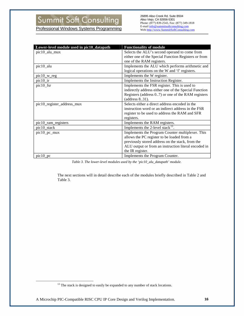
Table 2 below shows the highest-level modules used in the pic10_datapath module implementation. Table 3 shows the lower-level modules used (shown in parenthesis in Figure 5).
Highest-level module used in pic10_datapath Functionality of module pic10_alu_datapath Contains the ALU, W register as well as the ALU
multiplexer. The ALU multiplexer allows the ALU’s second operand to come from either the currently addressed RAM register or from the currently addressed SFR register.
pic10_sfr_datapath Contains the IR register, the FSR register, the RAM registers as well as a register address multiplexer. The Register Address Multiplexer allows the SFR/RAM registers to be addressed either via a literal in the instruction word or via the FSR register.
pic10_pc_datapath Contains the stack, the PC register as well as the PC Multiplexer. The PC Multiplexer allows the PC register to be either loaded from the stack, from the ALU output or from a literal in the instruction word.
pic10_status_reg Implements the STATUS register. Can either be parallel loaded from the ALU bus or individual bits can be set via the ‘status_bus’, ‘load_c’, ‘load_dc’ or ‘load_z’ inputs.
pic10_tri_state_port Implements bidirectional GPIO ports. Contains the TRIS and GPIO registers.
pic10_sfr_data_mux Selects data from one of the eight SFR registers and outputs it to the ‘sfr_data_bus’ which is connected to the ALU’s second operand multiplexer.
pic10_program_mux Allows either the actual next program instruction word or a hard coded NOP instruction word to be loaded into the IR register. This is used to ‘skip’ the next instruction (used by the DECFSZ, INCFSZ, BTFSC and BTFSS instructions).
Table 2. The highest-level modules used by the ‘pic10_alu_datapath’ module.
Professional Windows Systems Programming
A Microchip PIC-Compatible RISC CPU IP Core Design and Verilog Implementation. 16
26895 Aliso Creek Rd. Suite B504 Aliso Viejo, CA 92656-5301 Phone: (877) 839-2543, Fax: (877) 349-1818 E-mail [email protected] Web http://www.SummitSoftConsulting.com
Lower-level module used in pic10_datapath Functionality of module pic10_alu_mux Selects the ALU’s second operand to come from
either one of the Special Function Registers or from one of the RAM registers.
pic10_alu Implements the ALU which performs arithmetic and logical operations on the W and ‘f’ registers.
pic10_w_reg Implements the W register. pic10_ir Implements the Instruction Register. pic10_fsr Implements the FSR register. This is used to
indirectly address either one of the Special Function Registers (address 0..7) or one of the RAM registers (address 8..31).
pic10_register_address_mux Selects either a direct address encoded in the instruction word or an indirect address in the FSR register to be used to address the RAM and SFR registers.
pic10_ram_registers Implements the RAM registers. pic10_stack Implements the 2-level stack13. pic10_pc_mux Implements the Program Counter multiplexer. This
allows the PC register to be loaded from a previously stored address on the stack, from the ALU output or from an instruction literal encoded in the IR register.
pic10_pc Implements the Program Counter. Table 3. The lower-level modules used by the ‘pic10_alu_datapath’ module.
The next sections will in detail describe each of the modules briefly described in Table 2 and Table 3.
13 The stack is designed to easily be expanded to any number of stack locations.

Professional Windows Systems Programming
A Microchip PIC-Compatible RISC CPU IP Core Design and Verilog Implementation. 17
26895 Aliso Creek Rd. Suite B504 Aliso Viejo, CA 92656-5301 Phone: (877) 839-2543, Fax: (877) 349-1818 E-mail [email protected] Web http://www.SummitSoftConsulting.com
2.2.5. ALU Datapath (pic10_alu_datapath) Figure 6 below shows the internal architecture of the ‘pic10_alu_datapath’ module.
Figure 6. The contents of the ‘pic10_alu_datapath’ module. The module contains a datapath that feeds operands to the ALU and that outputs the result and status bits.
As shown in Figure 6, the ‘pic10_alu_datapath’ module contains the datapath logic required to route data to and from the ALU. The first operand of the ALU always comes from the W register. The second ALU operand comes from either the currently addressed RAM register (‘f’ register 0..7) or from the currently addressed Special Function Register (‘f’ register 8..31). The ‘pic10_datapath’ module will assert the ‘alu_mux_sel’ input whenever an ‘f’ register with address 8..31 is the source of destination of an instruction (i.e. when a RAM register is addressed).
The ALU knows which operation to perform from the instruction word input on ‘ir_reg_bus’. The ‘carry_bit’ input comes from the ‘C’ bit in the STATUS register and it is used as carry-in in Addition and Subtraction operations. The ‘status_bus’, ‘load_c’, ‘load_dc’ and ‘load_z’ outputs are used to update the status register flags based on the result of the ALU operation. The ‘status_bus’ carry the actual status bits and the ‘load_x’ signals tell the STATUS register which status bits to actually load (the different instructions update different status register bits).
The ‘alu_bus’ output is routed to all registers that can be the target of instructions. Note that the ALU only uses combinatorial logic. I.e. the ALU outputs changes immediately whenever any of the input signals change without waiting for the clock signal. Since all inputs change on the falling edge of ‘clock’ and the output signals are clocked in on the rising edge there will not be any race conditions resulting from the combinational ALU logic.
2.2.6. Special Function Register Datapath (pic10_sfr_datapath) The PIC10 architecture allows the ‘f’ registers to be addressed either directly via the 5-bit literal ‘fffff’ fields in the instruction word or indirectly via the value in the FSR register. This means that we need datapath logic to use either the ‘fffff’ field in the IR register or the value

Professional Windows Systems Programming
A Microchip PIC-Compatible RISC CPU IP Core Design and Verilog Implementation. 18
26895 Aliso Creek Rd. Suite B504 Aliso Viejo, CA 92656-5301 Phone: (877) 839-2543, Fax: (877) 349-1818 E-mail [email protected] Web http://www.SummitSoftConsulting.com
in the SFR register as address to the RAM registers and SFR registers. This is the purpose of the ‘pic10_sfr_datapath’ shown below in Figure 7.
Figure 7. The ‘pic10_sfr_datapath’ module contains the logic which generates the addresses to the RAM registers and the SFR Registers.
As can be seen in Figure 7, the Register Address Multiplexer passes through either the ‘fffff’ field in the instruction word (bits 4:0) or the value in the SFR register. The ‘reg_addr_mux_sel’ signal14 determines which source bus to route to ‘reg_addr_bus’.
The ‘program_mux_bus’ input15 bus allows the IR register to be loaded with the currently addressed instruction word when the ‘load_ir_reg’ signal is asserted. The ‘load_ram_reg’ signal will cause the data on ‘alu_bus’ to be loaded into the currently addressed16 RAM register. The RAM Register is constantly outputting its currently addressed register data onto ‘ram_data_bus’. The RAM registers were placed inside the ‘pic10_sfr_datapath’ module to enable the testing of the register addressing, i.e. that data can be written and read back from the RAM registers by using both the direct and indirect addressing modes in the ‘pic10_sfr_datapath.
Note that the ‘fsr_reg_bus’ output bus is connected to the controller in the higher-level ‘pic10_datapath’ module. This enables the controller to know which indirect address is used and therefore the controller will be able to assert the ‘load’ signal of the target ‘f’ register. Also note that all ‘load’ signals are asserted on the negative edge of the clock signal while all registers clock in data on the positive edge of ‘clock’.
14 Asserted when SFR register 0 is the source or destination ‘f’ register. 15 See section 2.1.11 for more information about the ‘program_mux_bus’ bus. 16 Via ir_reg_bus[4:0] or fsr_reg_bus[4:0].
Professional Windows Systems Programming
A Microchip PIC-Compatible RISC CPU IP Core Design and Verilog Implementation. 19
26895 Aliso Creek Rd. Suite B504 Aliso Viejo, CA 92656-5301 Phone: (877) 839-2543, Fax: (877) 349-1818 E-mail [email protected] Web http://www.SummitSoftConsulting.com
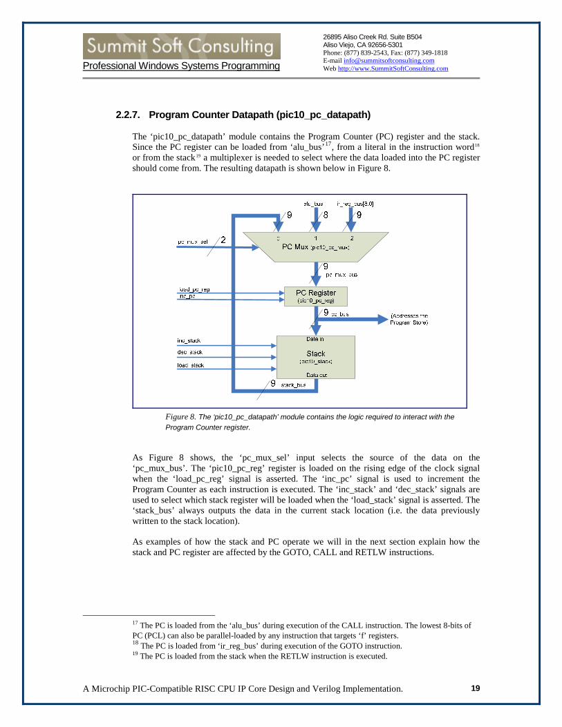
2.2.7. Program Counter Datapath (pic10_pc_datapath) The ‘pic10_pc_datapath’ module contains the Program Counter (PC) register and the stack. Since the PC register can be loaded from ‘alu_bus’17, from a literal in the instruction word18 or from the stack19 a multiplexer is needed to select where the data loaded into the PC register should come from. The resulting datapath is shown below in Figure 8.
Figure 8. The ‘pic10_pc_datapath’ module contains the logic required to interact with the Program Counter register.
As Figure 8 shows, the ‘pc_mux_sel’ input selects the source of the data on the ‘pc_mux_bus’. The ‘pic10_pc_reg’ register is loaded on the rising edge of the clock signal when the ‘load_pc_reg’ signal is asserted. The ‘inc_pc’ signal is used to increment the Program Counter as each instruction is executed. The ‘inc_stack’ and ‘dec_stack’ signals are used to select which stack register will be loaded when the ‘load_stack’ signal is asserted. The ‘stack_bus’ always outputs the data in the current stack location (i.e. the data previously written to the stack location).
As examples of how the stack and PC operate we will in the next section explain how the stack and PC register are affected by the GOTO, CALL and RETLW instructions.
17 The PC is loaded from the ‘alu_bus’ during execution of the CALL instruction. The lowest 8-bits of PC (PCL) can also be parallel-loaded by any instruction that targets ‘f’ registers. 18 The PC is loaded from ‘ir_reg_bus’ during execution of the GOTO instruction. 19 The PC is loaded from the stack when the RETLW instruction is executed.

Professional Windows Systems Programming
A Microchip PIC-Compatible RISC CPU IP Core Design and Verilog Implementation. 20
26895 Aliso Creek Rd. Suite B504 Aliso Viejo, CA 92656-5301 Phone: (877) 839-2543, Fax: (877) 349-1818 E-mail [email protected] Web http://www.SummitSoftConsulting.com
2.2.7.1. The GOTO instruction’s effect on the Stack and Program Counter The GOTO instruction jumps to the target program address by loading the 9-bit ‘kkkkkkkkk’ instruction word literal into the PC Register (see the instruction encoding in the Microchip PIC10F20x Data Sheet). This causes the target address to be output on the ‘pc_bus’ bus which in turn will cause the instruction at the target address to be output from the Program Store on the ‘program_bus’ bus. The Controller then loads the PC register with the 9-bit literal value by selecting input 2 on the PC Multiplexer and asserting ‘load_pc_reg’. No return address is stored on the stack by the GOTO instruction so the stack is never modified. The GOTO instruction is a two-cycle instruction because one cycle is needed to load the PC Register with the target address while a second cycle is needed to load the IR register with the target instruction. See Table 4 below for the signals asserted in the ‘pic10_pc_datapath’ module during the execution of the GOTO instruction.
Cycle Signal value Comment 1 pc_mux_sel = 2 pc_mux_bus = ir_reg_bus[8:0]. Note that the
target address is coming from the lowest 9-bits of the instruction word. Also note that 9 bits are being loaded which allows a jump to anywhere in the 9-bit address space.
1 load_pc_reg = 1 The PC Register is loaded with the 8-bit target address on the next rising clock edge.
2 load_ir_reg = 1 Loads the target instruction into the IR register.
Table 4. The stack and PC related signals asserted during a GOTO instruction.
2.2.7.2. The CALL instruction’s effect on the Stack and Program Counter Unlike the GOTO instruction, the CALL instruction saves the return address on the stack before loading the PC with the target address. Like the GOTO instruction, the CALL instruction is a two cycle instruction. See Table 5 below for the signals asserted in the ‘pic10_pc_datapath’ module during the execution of the CALL instruction20.
20 The same signals are asserted as for the GOTO instruction with the addition of the stack-related signals.

Professional Windows Systems Programming
A Microchip PIC-Compatible RISC CPU IP Core Design and Verilog Implementation. 21
26895 Aliso Creek Rd. Suite B504 Aliso Viejo, CA 92656-5301 Phone: (877) 839-2543, Fax: (877) 349-1818 E-mail [email protected] Web http://www.SummitSoftConsulting.com
Cycle Signal value Comment 1 pc_mux_sel = 1 pc_mux_bus = alu_bus. Note that only 8-bits
are being loaded which limits calls to the first 255 instruction words. Also note that the 8-bit target address is output by the ALU via ‘alu_bus’ and not via ir_reg_bus[8:0] like in the case of the GOTO instruction.
1 load_pc_reg = 1 The PC Register is loaded with the 8-bit target address on the next rising clock edge.
1 load_stack=1 The PC is saved onto the stack. Note that the PC contains the program address of the next instruction21.
2 load_ir_reg = 1 Loads the target instruction into the IR register.
2 dec_stack = 1 Decrements the stack to the next free stack location22.
Table 5. The stack and PC related signals asserted during a CALL instruction.
2.2.7.3. The RETLW instruction’s effect on the Stack and Program Counter The RETLW instruction is used to return to the previous execution location after a subroutine jumped to via the CALL instruction has been completed. The RETLW instruction loads the 8-bit literal encoded in the instruction word into the W register and pops the saved return address off the stack into the PC. The execution then continues where it left off when the CALL instruction previously was executed. Table 6 below shows the signals asserted during the execution of the RETLW instruction.
Cycle Signal value Comment 1 dec_stack = 1 Decrement the stack pointer so the previously
stored return address is output on 'stack_bus'. 2 pc_mux_sel = 0 Route ‘stack_bus’ to pc_mux_bus’ from
where the PC can load the return address. 2 load_pc_reg = 1 Load PC with the previously saved return
address on ‘stack_bus’. 3 load_ir_reg = 1 Loads the return instruction into the IR
register. Table 6. The stack and PC related signals asserted during a RETLW instruction.
Note that our implementation of the RETLW instruction takes three cycles while the Microchip PIC10 implementation takes two cycles. A three-cycle implementation was chosen because this enabled us to create a generic stack where the stack depth easily can be increased to a level more than two like in the original PIC10 Microchip architecture.
21 Recall from figure 1 that the Instruction Register contains the current instruction while the Program Counter contains the address of the next instruction to be executed. 22 The stack is by default 2-levels deep. The stack depth can be increased by changing the STACK_DEPTH definition at the top of the datapath.v Verilog file.

Professional Windows Systems Programming
A Microchip PIC-Compatible RISC CPU IP Core Design and Verilog Implementation. 22
26895 Aliso Creek Rd. Suite B504 Aliso Viejo, CA 92656-5301 Phone: (877) 839-2543, Fax: (877) 349-1818 E-mail [email protected] Web http://www.SummitSoftConsulting.com
Note: The RETLW instruction also loads an 8-bit constant into the W register in cycle 3 by asserting the ‘load_w_reg’ signal. The constant is routed from the IR register, via the ALU and into the W register.
2.2.8. Status Register module (pic10_status_reg) Since the ALU needs to update the C, DC and Z flags in the STATUS register, we require an additional 3-bit output bus called ‘status_bus’ between the ALU and the STATUS register (shown below in Figure 9). The STATUS register then updates the required status bits depending on which of the ‘load_c’, ‘load_dc’ and ‘load_z’ are asserted.
Figure 9. The ALU updates the STATUS register flags via the status_bus bus and the load_c, load_dc and load_z signals.
Also note in Figure 9 that the STATUS register can be parallel loaded with data from ‘alu_bus’ by any instruction that has an ‘f’ register as potential target. This means that the STATUS register can potentially be loaded at the same time from the ‘status_bus’ and ‘alu_bus’ inputs. This happens when the STATUS register, which is accessible as Special Function Register 3, is the target of an operation that also modifies the STATUS register flags (virtually all instructions in table 10-2 ‘Instruction Set Summary’ in the Microchip PIC10F200 Datasheet). As pointed out in the Microchip PIC10F100 datasheet, the C, DC and Z bits in the STATUS register are not written if the instruction executed is also updating the status bits. This is handled in the STATUS register implementation by ignoring the ‘load_c’, ‘load_dc’ and ‘load_z’ input in case the ‘load_status_reg’ input is also asserted.
2.2.9. Tri-State GPIO Port module (pic10_tri_state_port) The PIC10 CPU IP Core contains three bidirectional 8-bit I/O ports while the Microchip PIC10F20x architecture only has a single GPIO register (where only 4 bits are implemented due to lack of pins on the package). The I/O port bits can individually be programmed as input or output via the TRIS instruction. The output data (for output ports) is programmed into GPIO registers 5, 6 and 7 (where GPIO registers 5 and 7 replaces the not implemented OSCCAL and CMCON0 registers).

Professional Windows Systems Programming
A Microchip PIC-Compatible RISC CPU IP Core Design and Verilog Implementation. 23
26895 Aliso Creek Rd. Suite B504 Aliso Viejo, CA 92656-5301 Phone: (877) 839-2543, Fax: (877) 349-1818 E-mail [email protected] Web http://www.SummitSoftConsulting.com
Figure 10 below shows the internal architecture of the ‘pic10_tri_state_port’ module. As can be seen, the ‘alu_bus’ input allows the TRIS and GPIO 8-bit registers to be loaded from ‘alu_bus. A TRIS registers (5, 6 or 7) is loaded from ‘alu_bus’ when a TRIS instruction is executed. A GPIO register (5, 6 or 7) is loaded when Special Function Registers 5, 6 or 7 is the write target of an instruction (i.e. MOVWF).
Figure 10. The ‘pic10_tri_state_port’ module contains the 8-bit bi-directional I/O port logic.
Figure 10 doesn’t show the gate-level details of how the tri-state port is implemented so Figure 11 below shows a more detailed view of the implementation for a single I/O bit.
Figure 11. The gate-level implementation of a single bi-directional I/O port pin.
As can be seen in Figure 11, the GPIO register bit ‘gpio_reg’ is gated via a tri-state buffer that is controlled via the TRIS register bit ‘tris_reg’. The result is that the output pin ‘gpio_pin_bus’ will only be driven from the GPIO register bit if the corresponding TRIS register bit is 0. In order to be able to read from an input pin, the ‘gpio_pin_bus’ signal is gated via another tri-state buffer onto the ‘triport_bus’ output which is the actual bus routed to the ALU when GPIO register 5, 6 or 7 is read. Note that the upper tri-state buffer lets the GPIO register bit through when the corresponding TRIS register bit is clear while the lower tri-state buffer lets the ‘gpio_pin_bus’ through when the corresponding TRIS register is low. The TRIS register bits are all set to FFh at reset so all I/O bits will by default be input bits.
For a different perspective of the pic10_tri_state_port implementation please also see the Verilog source code in section 3.2.17.

Professional Windows Systems Programming
A Microchip PIC-Compatible RISC CPU IP Core Design and Verilog Implementation. 24
26895 Aliso Creek Rd. Suite B504 Aliso Viejo, CA 92656-5301 Phone: (877) 839-2543, Fax: (877) 349-1818 E-mail [email protected] Web http://www.SummitSoftConsulting.com
2.2.10. SFR Data Multiplexer module (pic10_sfr_data_mux) The SFR Data Multiplexer is used to route the output of the currently addressed SFR register (‘f’ register 0..7) to the ALU Multiplexer’s second operand. Since all SFR registers are 8-bits wide the SFR Multiplexer is an 8-1 8-bit multiplexer. Figure 12 below shows the inputs and outputs of the SFR multiplexer.
Figure 12. The ‘pic10_sfr_data_mux’ module selects one of the SFR register outputs to be routed to the ALU Multiplexer as a source operand.
Note that inputs 0 (INDF) and 1 (TMR0) both read as 00h because these registers are not implemented. A read from the INDF register will cause the data to be supplied by one of the other SFR registers23. See Figure 6 (ALU datapath) too see how the ‘sfr_mux_bus’ output is connected to the ALU datapath.
2.2.11. Program Bus Multiplexer module (pic10_program_mux) Certain instructions in the PIC10’s instruction set results in the next instruction to be treated as a NOP under certain conditions. These instructions are the DECFSZ, INCFSZ, BTFSC and BTFSS instructions. See the Microchip PIC10F200/202/204/206 Data Sheet for details under which conditions these instructions will cause the next instruction to be interpreted as a NOP.
When an instruction should be treated as a NOP, the Program Bus Multiplexer will select a hard-coded NOP instruction (000h) to be loaded into the IR register instead of the actually addressed instruction in the Program Store. Figure 13 below shows the inputs and outputs of the Program Bus Multiplexer.
23 This is indirect addressing. See section 4.9 in the Microchip PIC10F20x datasheet.

Professional Windows Systems Programming
A Microchip PIC-Compatible RISC CPU IP Core Design and Verilog Implementation. 25
26895 Aliso Creek Rd. Suite B504 Aliso Viejo, CA 92656-5301 Phone: (877) 839-2543, Fax: (877) 349-1818 E-mail [email protected] Web http://www.SummitSoftConsulting.com
Figure 13. The ‘pic10_program_mux’ module is used to force a NOP instruction to be loaded into the IR register as the consequence of the previous instruction being a ‘skip’-instruction.
The controller will during load of the IR register assert the ‘program_mux_sel’ input if the previous instruction should cause the current instruction to be treated as a NOP. This causes the ‘nop_bus’ input in Figure 13 to be routed to the ‘program_mux_bus’ output. See Figure 7 for an illustration of where the ‘program_mux_bus’ output is routed to.

Professional Windows Systems Programming
A Microchip PIC-Compatible RISC CPU IP Core Design and Verilog Implementation. 26
26895 Aliso Creek Rd. Suite B504 Aliso Viejo, CA 92656-5301 Phone: (877) 839-2543, Fax: (877) 349-1818 E-mail [email protected] Web http://www.SummitSoftConsulting.com
2.3. Controller Architecture As shown in Figure 1 on page 9, the ‘pic10_controller’ module is connected via a number of inputs and outputs to the ‘pic10_datapath’ module. The controller is responsible for decoding the current instruction in the IR register and set up the datapath control signals so that the data is correctly routed from the source to the destination register accordingly to the semantics of the instruction. As the instruction in the IR changes so does the functionality of the Controller. The Controller is essentially a simple state machine that asserts a pre-determined number of signals for the various instructions. Figure 14 below shows the inputs and outputs of the ‘pic10_controller’ module.
Figure 14. The input and output signals on the Controller module.
The following sections describe the datapath control signals that need to be asserted for each instruction. The path the data is routed from the source to the destination register will be illustrated via the block diagrams earlier in this chapter as well as via pseudo Verilog code. Please refer to the Microchip PIC10F200/202/204/206 data sheet for the detailed syntax and description of the various instructions.
Professional Windows Systems Programming
A Microchip PIC-Compatible RISC CPU IP Core Design and Verilog Implementation. 27
26895 Aliso Creek Rd. Suite B504 Aliso Viejo, CA 92656-5301 Phone: (877) 839-2543, Fax: (877) 349-1818 E-mail [email protected] Web http://www.SummitSoftConsulting.com
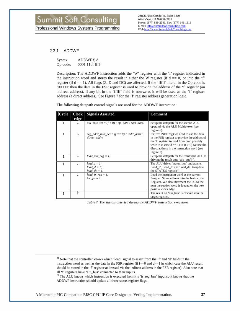
2.3.1. ADDWF Syntax: ADDWF f, d Op-code: 0001 11df ffff Description: The ADDWF instruction adds the ‘W’ register with the ‘f’ register indicated in the instruction word and stores the result in either the W register (if d == 0) or into the ‘f’ register (if d == 1). All flags (Z, D and DC) are affected. If the ‘fffff’ literal in the Op-code is ‘00000’ then the data in the FSR register is used to provide the address of the ‘f’ register (an indirect address). If any bit in the ‘fffff’ field is non-zero, it will be used as the ‘f’ register address (a direct address). See Figure 7 for the ‘f’ register address generation logic.
The following datapath control signals are used for the ADDWF instruction:
Cycle Clock edge
Signals Asserted Comment
1 ↓ alu_mux_sel = (f < 8) ? sfr_data : ram_data;
Setup the datapath for the second ALU operand via the ALU Multiplexer (see Figure 6).
1 ↓ reg_addr_mux_sel = (f == 0) ? indir_addr : direct_addr;
If (f == INDF reg) we need to use the data in the FSR register to provide the address of the ‘f’ register to read from (and possibly write to in case d == 1). If (f > 0) we use the direct address in the instruction word (see Figure 7).
1 ↓ load_xxx_reg = 1; Setup the datapath for the result (the ALU is driving the result onto ‘alu_bus’)24.
1 ↓ load_z = 1; load_d = 1; load_dc = 1;
The ALU drives ‘status_bus’ and asserts ‘load_z’, ‘load_d’ and ‘load_dc’ to update the STATUS register25.
1 ↓ load_ir_reg = 1; inc_pc = 1;
Load the instruction word at the current Program Store address into the Instruction Register. We also increment the PC so the next instruction word is loaded on the next positive clock edge.
1 ↑ The result on ‘alu_bus’ is clocked into the target register.
Table 7. The signals asserted during the ADDWF instruction execution.
24 Note that the controller knows which ‘load’ signal to assert from the ‘f’ and ‘d’ fields in the instruction word as well as the data in the FSR register (if f==0 and d==1 in which case the ALU result should be stored in the ‘f’ register addressed via the indirect address in the FSR register). Also note that all ‘f’ registers have ‘alu_bus’ connected to their inputs. 25 The ALU knows which instruction is executed from it’s ‘ir_reg_bus’ input so it knows that the ADDWF instruction should update all three status register flags.
Professional Windows Systems Programming
A Microchip PIC-Compatible RISC CPU IP Core Design and Verilog Implementation. 28
26895 Aliso Creek Rd. Suite B504 Aliso Viejo, CA 92656-5301 Phone: (877) 839-2543, Fax: (877) 349-1818 E-mail [email protected] Web http://www.SummitSoftConsulting.com
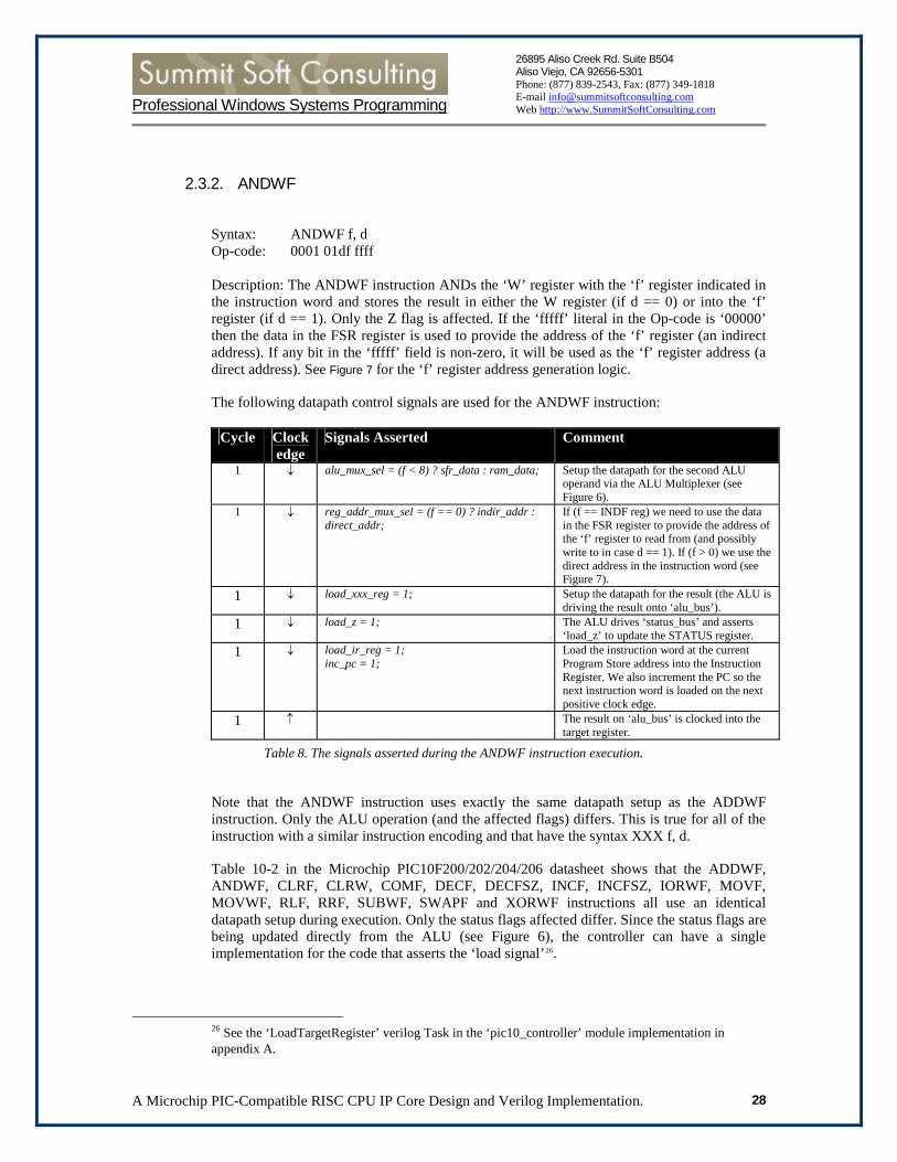
2.3.2. ANDWF
Syntax: ANDWF f, d Op-code: 0001 01df ffff Description: The ANDWF instruction ANDs the ‘W’ register with the ‘f’ register indicated in the instruction word and stores the result in either the W register (if d == 0) or into the ‘f’ register (if d == 1). Only the Z flag is affected. If the ‘fffff’ literal in the Op-code is ‘00000’ then the data in the FSR register is used to provide the address of the ‘f’ register (an indirect address). If any bit in the ‘fffff’ field is non-zero, it will be used as the ‘f’ register address (a direct address). See Figure 7 for the ‘f’ register address generation logic.
The following datapath control signals are used for the ANDWF instruction:
Cycle Clock edge
Signals Asserted Comment
1 ↓ alu_mux_sel = (f < 8) ? sfr_data : ram_data;
Setup the datapath for the second ALU operand via the ALU Multiplexer (see Figure 6).
1 ↓ reg_addr_mux_sel = (f == 0) ? indir_addr : direct_addr;
If (f == INDF reg) we need to use the data in the FSR register to provide the address of the ‘f’ register to read from (and possibly write to in case d == 1). If (f > 0) we use the direct address in the instruction word (see Figure 7).
1 ↓ load_xxx_reg = 1; Setup the datapath for the result (the ALU is driving the result onto ‘alu_bus’).
1 ↓ load_z = 1; The ALU drives ‘status_bus’ and asserts ‘load_z’ to update the STATUS register.
1 ↓ load_ir_reg = 1; inc_pc = 1;
Load the instruction word at the current Program Store address into the Instruction Register. We also increment the PC so the next instruction word is loaded on the next positive clock edge.
1 ↑ The result on ‘alu_bus’ is clocked into the target register.
Table 8. The signals asserted during the ANDWF instruction execution.
Note that the ANDWF instruction uses exactly the same datapath setup as the ADDWF instruction. Only the ALU operation (and the affected flags) differs. This is true for all of the instruction with a similar instruction encoding and that have the syntax XXX f, d.
Table 10-2 in the Microchip PIC10F200/202/204/206 datasheet shows that the ADDWF, ANDWF, CLRF, CLRW, COMF, DECF, DECFSZ, INCF, INCFSZ, IORWF, MOVF, MOVWF, RLF, RRF, SUBWF, SWAPF and XORWF instructions all use an identical datapath setup during execution. Only the status flags affected differ. Since the status flags are being updated directly from the ALU (see Figure 6), the controller can have a single implementation for the code that asserts the ‘load signal’26.
26 See the ‘LoadTargetRegister’ verilog Task in the ‘pic10_controller’ module implementation in appendix A.

Professional Windows Systems Programming
A Microchip PIC-Compatible RISC CPU IP Core Design and Verilog Implementation. 29
26895 Aliso Creek Rd. Suite B504 Aliso Viejo, CA 92656-5301 Phone: (877) 839-2543, Fax: (877) 349-1818 E-mail [email protected] Web http://www.SummitSoftConsulting.com
2.3.3. CLRF
Syntax: CLRF Op-code: 0000 011f ffff Description: The CLRF instruction loads 00h into the ‘f’ register indicated in the instruction word. Only the Z flag is affected27. If the ‘fffff’ literal in the Op-code is ‘00000’ then the data in the FSR register is used to provide the address of the ‘f’ register (an indirect address). If any bit in the ‘fffff’ field is non-zero, it will be used as the ‘f’ register address (a direct address). See Figure 7 for the ‘f’ register address generation logic.
The following datapath control signals are used for the CLRF instruction:
Cycle Clock edge
Signals Asserted Comment
1 ↓ alu_mux_sel = (f < 8) ? sfr_data : ram_data;
Setup the datapath for the second ALU operand via the ALU Multiplexer (see Figure 6).
1 ↓ reg_addr_mux_sel = (f == 0) ? indir_addr : direct_addr;
If (f == INDF reg) we need to use the data in the FSR register to provide the address of the ‘f’ register to clear. If (f > 0) we use the direct address in the instruction word (see Figure 7).
1 ↓ load_xxx_reg = 1; Setup the datapath for the result (the ALU is driving the result onto ‘alu_bus’).
1 ↓ load_z = 1; The ALU drives ‘status_bus’ and asserts ‘load_z’ to update the STATUS register.
1 ↓ load_ir_reg = 1; inc_pc = 1;
Load the instruction word at the current Program Store address into the Instruction Register. We also increment the PC so the next instruction word is loaded on the next positive clock edge.
1 ↑ The result on ‘alu_bus’ is clocked into the target register.
Table 9. The signals asserted during the CLRF instruction execution.
Note that the CLRF instruction uses exactly the same datapath setup as the ADDWF instruction. Only the ALU operation (and the affected flags) differs. On first look, the CLRF instruction appears to be different from the other instructions with the ‘XXX f, d’ instruction syntax. On closer examination of the Op-code, it is in fact using the same format as the other ‘XXX f, d’ instruction but the ‘d’ bit has been hard-coded to 1 (with the result that the ALU output – 00h in this case – will be loaded into the addressed ‘f’ register) 28 . The CLRW instruction is used to clear the ‘W’ register.
27 Note that the Z flag is always set since the target register is cleared. 28 Therefore, the controller uses the same ‘LoadTargetRegister’ Task to assert the ‘load_xxx_reg’ signal for the CLRF instruction as for all other instructions with the ‘XXX f, d’ syntax.

Professional Windows Systems Programming
A Microchip PIC-Compatible RISC CPU IP Core Design and Verilog Implementation. 30
26895 Aliso Creek Rd. Suite B504 Aliso Viejo, CA 92656-5301 Phone: (877) 839-2543, Fax: (877) 349-1818 E-mail [email protected] Web http://www.SummitSoftConsulting.com
2.3.4. CLRW
Syntax: CLRW Op-code: 0000 0100 0000 Description: The CLRW instruction loads 00h into the ‘W’ register. Only the Z flag is affected29.
The following datapath control signals are used for the CLRW instruction:
Cycle Clock edge
Signals Asserted Comment
1 ↓ load_w_reg = 1; Setup the datapath for the result (the ALU is driving the result onto ‘alu_bus’).
1 ↓ load_z = 1; The ALU drives ‘status_bus’ and asserts ‘load_z’ to update the STATUS register.
1 ↓ load_ir_reg = 1; inc_pc = 1;
Load the instruction word at the current Program Store address into the Instruction Register. We also increment the PC so the next instruction word is loaded on the next positive clock edge.
1 ↑ The result on ‘alu_bus’ is clocked into the ‘W’ register.
Table 10. The signals asserted during the CLRW instruction execution.
Note that the CLRW instruction uses a simpler datapath setup than the instructions with the ‘XXX f, d’ syntax. This is because the ALU directly outputs 00h and since the ‘W’ register directly is connected to the ALU only the ‘load_w_reg’ signal needs to be asserted to load the target register.
On first look, the CLRW instruction appears to be different from the other instructions with the ‘XXX f, d’ instruction syntax. On closer examination of the Op-code, it is in fact using the same format as the other ‘XXX f, d’ instruction but the ‘d’ bit has been hard-coded to 0 (with the result that the ALU output – 00h in this case – will be loaded into the ‘W’ register30.
29 Note that the Z flag is always set since the target register is cleared. 30 Therefore, the controller uses the same ‘LoadTargetRegister’ Task to assert the ‘load_wxxx_reg’ signal (in this case ‘load_w_reg’) for the CLRW instruction as for all other instructions with the ‘XXX f, d’ syntax.

Professional Windows Systems Programming
A Microchip PIC-Compatible RISC CPU IP Core Design and Verilog Implementation. 31
26895 Aliso Creek Rd. Suite B504 Aliso Viejo, CA 92656-5301 Phone: (877) 839-2543, Fax: (877) 349-1818 E-mail [email protected] Web http://www.SummitSoftConsulting.com
2.3.5. COMF
Syntax: COMF f, d Op-code: 0010 01df ffff Description: The COMF instruction complement31 the ‘f’ register indicated in the instruction word and stores the result in either the W register (if d == 0) or into the ‘f’ register (if d == 1). Only the Z flag is affected. If the ‘fffff’ literal in the Op-code is ‘00000’ then the data in the FSR register is used to provide the address of the ‘f’ register (an indirect address). If any bit in the ‘fffff’ field is non-zero, it will be used as the ‘f’ register address (a direct address). See Figure 7 for the ‘f’ register address generation logic.
The following datapath control signals are used for the COMF instruction:
Cycle Clock edge
Signals Asserted Comment
1 ↓ alu_mux_sel = (f < 8) ? sfr_data : ram_data;
Setup the datapath for the second ALU operand via the ALU Multiplexer (see Figure 6).
1 ↓ reg_addr_mux_sel = (f == 0) ? indir_addr : direct_addr;
If (f == INDF reg) we need to use the data in the FSR register to provide the address of the ‘f’ register to read from (and possibly write to in case d == 1). If (f > 0) we use the direct address in the instruction word (see Figure 7).
1 ↓ load_xxx_reg = 1; Setup the datapath for the result (the ALU is driving the result onto ‘alu_bus’).
1 ↓ load_z = 1; The ALU drives ‘status_bus’ and asserts ‘load_z’ to update the STATUS register.
1 ↓ load_ir_reg = 1; inc_pc = 1;
Load the instruction word at the current Program Store address into the Instruction Register. We also increment the PC so the next instruction word is loaded on the next positive clock edge.
1 ↑ The result on ‘alu_bus’ is clocked into the target register.
Table 11. The signals asserted during the COMF instruction execution.
Note that the COMF instruction uses exactly the same datapath setup as the ADDWF instruction. Only the ALU operation and the affected status register flags differ32.
31 Inverts all bits. 32 See the ADDWF and ANDWF instructions earlier in this chapter for more details regarding common instruction field encoding.

Professional Windows Systems Programming
A Microchip PIC-Compatible RISC CPU IP Core Design and Verilog Implementation. 32
26895 Aliso Creek Rd. Suite B504 Aliso Viejo, CA 92656-5301 Phone: (877) 839-2543, Fax: (877) 349-1818 E-mail [email protected] Web http://www.SummitSoftConsulting.com
2.3.6. DECF
Syntax: DECF f, d Op-code: 0000 11df ffff Description: The DECF instruction decrements the ‘f’ register indicated in the instruction word and stores the result in either the W register (if d == 0) or into the ‘f’ register (if d == 1). Only the Z flag is affected. If the ‘fffff’ literal in the Op-code is ‘00000’ then the data in the FSR register is used to provide the address of the ‘f’ register (an indirect address). If any bit in the ‘fffff’ field is non-zero, it will be used as the ‘f’ register address (a direct address). See Figure 7 for the ‘f’ register address generation logic.
The following datapath control signals are used for the DECF instruction:
Cycle Clock
edge Signals Asserted Comment
1 ↓ alu_mux_sel = (f < 8) ? sfr_data : ram_data;
Setup the datapath for the second ALU operand via the ALU Multiplexer (see Figure 6).
1 ↓ reg_addr_mux_sel = (f == 0) ? indir_addr : direct_addr;
If (f == INDF reg) we need to use the data in the FSR register to provide the address of the ‘f’ register to read from (and possibly write to in case d == 1). If (f > 0) we use the direct address in the instruction word (see Figure 7).
1 ↓ load_xxx_reg = 1; Setup the datapath for the result (the ALU is driving the result onto ‘alu_bus’).
1 ↓ load_z = 1; The ALU drives ‘status_bus’ and asserts ‘load_z’ to update the STATUS register.
1 ↓ load_ir_reg = 1; inc_pc = 1;
Load the instruction word at the current Program Store address into the Instruction Register. We also increment the PC so the next instruction word is loaded on the next positive clock edge.
1 ↑ The result on ‘alu_bus’ is clocked into the target register.
Table 12. The signals asserted during the DECF instruction execution.
Note that the DECF instruction uses exactly the same datapath setup as the ADDWF instruction. Only the ALU operation and the affected status register flags differ33.
33 See the ADDWF and ANDWF instructions earlier in this chapter for more details regarding common instruction field encoding.
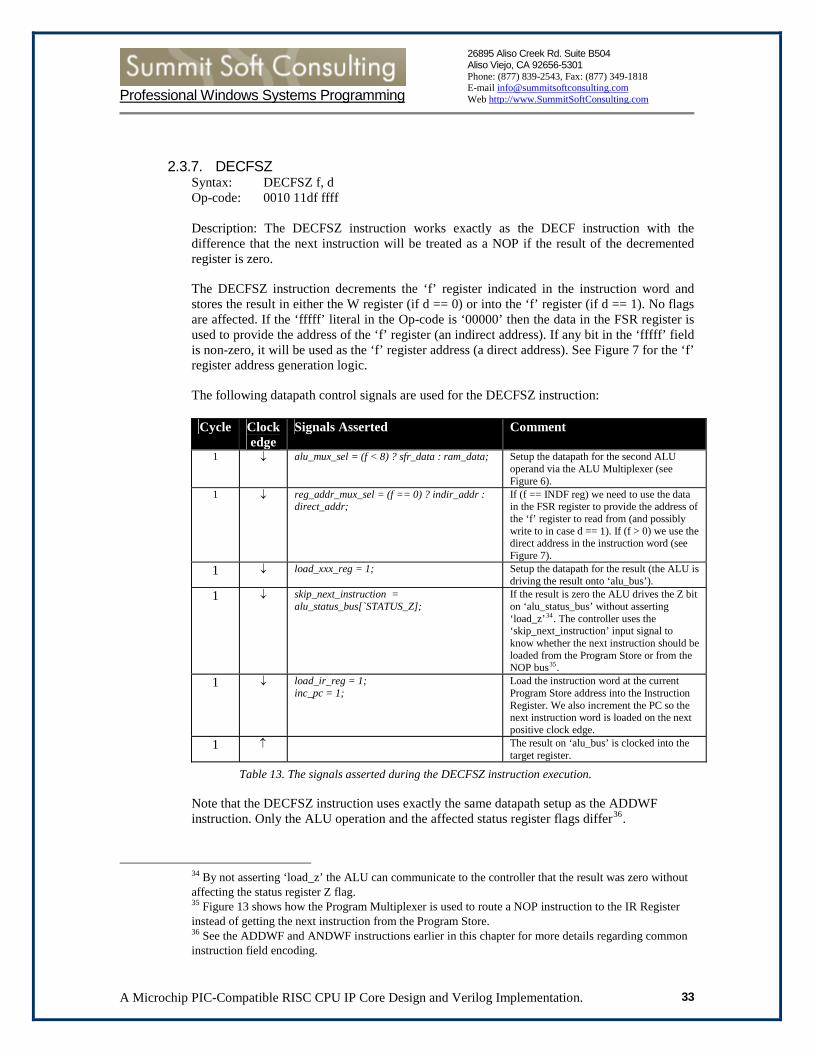
Professional Windows Systems Programming
A Microchip PIC-Compatible RISC CPU IP Core Design and Verilog Implementation. 33
26895 Aliso Creek Rd. Suite B504 Aliso Viejo, CA 92656-5301 Phone: (877) 839-2543, Fax: (877) 349-1818 E-mail [email protected] Web http://www.SummitSoftConsulting.com
2.3.7. DECFSZ Syntax: DECFSZ f, d Op-code: 0010 11df ffff Description: The DECFSZ instruction works exactly as the DECF instruction with the difference that the next instruction will be treated as a NOP if the result of the decremented register is zero.
The DECFSZ instruction decrements the ‘f’ register indicated in the instruction word and stores the result in either the W register (if d == 0) or into the ‘f’ register (if d == 1). No flags are affected. If the ‘fffff’ literal in the Op-code is ‘00000’ then the data in the FSR register is used to provide the address of the ‘f’ register (an indirect address). If any bit in the ‘fffff’ field is non-zero, it will be used as the ‘f’ register address (a direct address). See Figure 7 for the ‘f’ register address generation logic.
The following datapath control signals are used for the DECFSZ instruction:
Cycle Clock edge
Signals Asserted Comment
1 ↓ alu_mux_sel = (f < 8) ? sfr_data : ram_data;
Setup the datapath for the second ALU operand via the ALU Multiplexer (see Figure 6).
1 ↓ reg_addr_mux_sel = (f == 0) ? indir_addr : direct_addr;
If (f == INDF reg) we need to use the data in the FSR register to provide the address of the ‘f’ register to read from (and possibly write to in case d == 1). If (f > 0) we use the direct address in the instruction word (see Figure 7).
1 ↓ load_xxx_reg = 1; Setup the datapath for the result (the ALU is driving the result onto ‘alu_bus’).
1 ↓ skip_next_instruction = alu_status_bus[`STATUS_Z];
If the result is zero the ALU drives the Z bit on ‘alu_status_bus’ without asserting ‘load_z’34. The controller uses the ‘skip_next_instruction’ input signal to know whether the next instruction should be loaded from the Program Store or from the NOP bus35.
1 ↓ load_ir_reg = 1; inc_pc = 1;
Load the instruction word at the current Program Store address into the Instruction Register. We also increment the PC so the next instruction word is loaded on the next positive clock edge.
1 ↑ The result on ‘alu_bus’ is clocked into the target register.
Table 13. The signals asserted during the DECFSZ instruction execution.
Note that the DECFSZ instruction uses exactly the same datapath setup as the ADDWF instruction. Only the ALU operation and the affected status register flags differ36.
34 By not asserting ‘load_z’ the ALU can communicate to the controller that the result was zero without affecting the status register Z flag. 35 Fig shows how the Program Multiplexer is used to route a NOP instruction to the IR Register instead of getting the next instruction from the Program Store.
ure 13
36 See the ADDWF and ANDWF instructions earlier in this chapter for more details regarding common instruction field encoding.

Professional Windows Systems Programming
A Microchip PIC-Compatible RISC CPU IP Core Design and Verilog Implementation. 34
26895 Aliso Creek Rd. Suite B504 Aliso Viejo, CA 92656-5301 Phone: (877) 839-2543, Fax: (877) 349-1818 E-mail [email protected] Web http://www.SummitSoftConsulting.com
2.3.8. INCF
Syntax: INCF f, d Op-code: 0010 10df ffff Description: The INCF instruction increments the ‘f’ register indicated in the instruction word and stores the result in either the W register (if d == 0) or into the ‘f’ register (if d == 1). Only the Z flag is affected. If the ‘fffff’ literal in the Op-code is ‘00000’ then the data in the FSR register is used to provide the address of the ‘f’ register (an indirect address). If any bit in the ‘fffff’ field is non-zero, it will be used as the ‘f’ register address (a direct address). See Figure 7 for the ‘f’ register address generation logic.
The following datapath control signals are used for the INCF instruction:
Cycle Clock edge
Signals Asserted Comment
1 ↓ alu_mux_sel = (f < 8) ? sfr_data : ram_data;
Setup the datapath for the second ALU operand via the ALU Multiplexer (see Figure 6).
1 ↓ reg_addr_mux_sel = (f == 0) ? indir_addr : direct_addr;
If (f == INDF reg) we need to use the data in the FSR register to provide the address of the ‘f’ register to read from (and possibly write to in case d == 1). If (f > 0) we use the direct address in the instruction word (see Figure 7).
1 ↓ load_xxx_reg = 1; Setup the datapath for the result (the ALU is driving the result onto ‘alu_bus’).
1 ↓ load_z = 1; The ALU drives ‘status_bus’ and asserts ‘load_z’ to update the STATUS register.
1 ↓ load_ir_reg = 1; inc_pc = 1;
Load the instruction word at the current Program Store address into the Instruction Register. We also increment the PC so the next instruction word is loaded on the next positive clock edge.
1 ↑ The result on ‘alu_bus’ is clocked into the target register.
Table 14. The signals asserted during the INCF instruction execution.
Note that the INCF instruction uses exactly the same datapath setup as the ADDWF instruction. Only the ALU operation and the affected status register flags differ37.
37 See the ADDWF and ANDWF instructions earlier in this chapter for more details regarding common instruction field encoding.

Professional Windows Systems Programming
A Microchip PIC-Compatible RISC CPU IP Core Design and Verilog Implementation. 35
26895 Aliso Creek Rd. Suite B504 Aliso Viejo, CA 92656-5301 Phone: (877) 839-2543, Fax: (877) 349-1818 E-mail [email protected] Web http://www.SummitSoftConsulting.com
2.3.9. INCFSZ Syntax: INCFSZ f, d Op-code: 0011 11df ffff Description: The INCFSZ instruction works exactly as the INCF instruction with the difference that the next instruction will be treated as a NOP if the result of the incremented register is zero.
The INCFSZ instruction increments the ‘f’ register indicated in the instruction word and stores the result in either the W register (if d == 0) or into the ‘f’ register (if d == 1). No flags are affected. If the ‘fffff’ literal in the Op-code is ‘00000’ then the data in the FSR register is used to provide the address of the ‘f’ register (an indirect address). If any bit in the ‘fffff’ field is non-zero, it will be used as the ‘f’ register address (a direct address). See Figure 7 for the ‘f’ register address generation logic.
The following datapath control signals are used for the INCFSZ instruction:
Cycle Clock edge
Signals Asserted Comment
1 ↓ alu_mux_sel = (f < 8) ? sfr_data : ram_data;
Setup the datapath for the second ALU operand via the ALU Multiplexer (see Figure 6).
1 ↓ reg_addr_mux_sel = (f == 0) ? indir_addr : direct_addr;
If (f == INDF reg) we need to use the data in the FSR register to provide the address of the ‘f’ register to read from (and possibly write to in case d == 1). If (f > 0) we use the direct address in the instruction word (see Figure 7).
1 ↓ load_xxx_reg = 1; Setup the datapath for the result (the ALU is driving the result onto ‘alu_bus’).
1 ↓ skip_next_instruction = alu_status_bus[`STATUS_Z];
If the result is zero the ALU drives the Z bit on ‘alu_status_bus’ without asserting ‘load_z’38. The controller uses the ‘skip_next_instruction’ input signal to know whether the next instruction should be loaded from the Program Store or from the NOP bus39.
1 ↓ load_ir_reg = 1; inc_pc = 1;
Load the instruction word at the current Program Store address into the Instruction Register. We also increment the PC so the next instruction word is loaded on the next positive clock edge.
1 ↑ The result on ‘alu_bus’ is clocked into the target register.
Table 15. The signals asserted during the INCFSZ instruction execution.
Note that the INCFSZ instruction uses exactly the same datapath setup as the ADDWF instruction. Only the ALU operation and the affected status register flags differ40.
38 By not asserting ‘load_z’ the ALU can communicate to the controller that the result was zero without affecting the status register Z flag. 39 Fig shows how the Program Multiplexer is used to route a NOP instruction to the IR Register instead of getting the next instruction from the Program Store.
ure 13
40 See the ADDWF and ANDWF instructions earlier in this chapter for more details regarding common instruction field encoding.
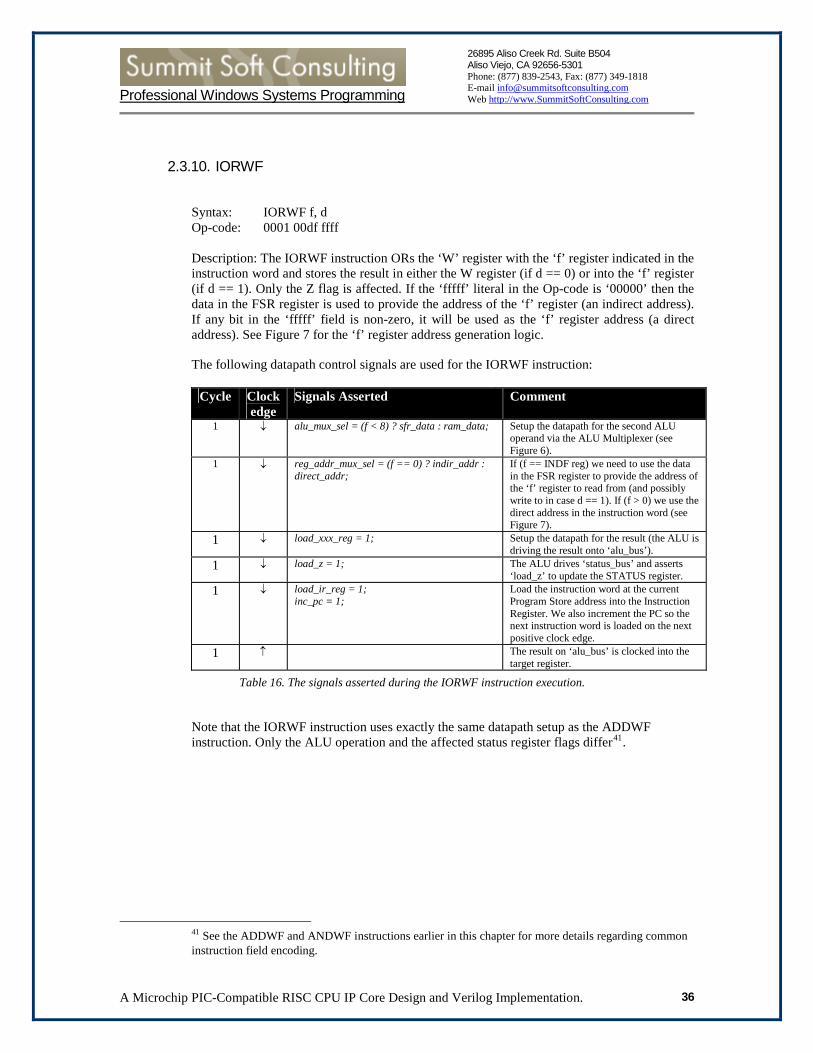
Professional Windows Systems Programming
A Microchip PIC-Compatible RISC CPU IP Core Design and Verilog Implementation. 36
26895 Aliso Creek Rd. Suite B504 Aliso Viejo, CA 92656-5301 Phone: (877) 839-2543, Fax: (877) 349-1818 E-mail [email protected] Web http://www.SummitSoftConsulting.com
2.3.10. IORWF
Syntax: IORWF f, d Op-code: 0001 00df ffff Description: The IORWF instruction ORs the ‘W’ register with the ‘f’ register indicated in the instruction word and stores the result in either the W register (if d == 0) or into the ‘f’ register (if d == 1). Only the Z flag is affected. If the ‘fffff’ literal in the Op-code is ‘00000’ then the data in the FSR register is used to provide the address of the ‘f’ register (an indirect address). If any bit in the ‘fffff’ field is non-zero, it will be used as the ‘f’ register address (a direct address). See Figure 7 for the ‘f’ register address generation logic.
The following datapath control signals are used for the IORWF instruction:
Cycle Clock edge
Signals Asserted Comment
1 ↓ alu_mux_sel = (f < 8) ? sfr_data : ram_data;
Setup the datapath for the second ALU operand via the ALU Multiplexer (see Figure 6).
1 ↓ reg_addr_mux_sel = (f == 0) ? indir_addr : direct_addr;
If (f == INDF reg) we need to use the data in the FSR register to provide the address of the ‘f’ register to read from (and possibly write to in case d == 1). If (f > 0) we use the direct address in the instruction word (see Figure 7).
1 ↓ load_xxx_reg = 1; Setup the datapath for the result (the ALU is driving the result onto ‘alu_bus’).
1 ↓ load_z = 1; The ALU drives ‘status_bus’ and asserts ‘load_z’ to update the STATUS register.
1 ↓ load_ir_reg = 1; inc_pc = 1;
Load the instruction word at the current Program Store address into the Instruction Register. We also increment the PC so the next instruction word is loaded on the next positive clock edge.
1 ↑ The result on ‘alu_bus’ is clocked into the target register.
Table 16. The signals asserted during the IORWF instruction execution.
Note that the IORWF instruction uses exactly the same datapath setup as the ADDWF instruction. Only the ALU operation and the affected status register flags differ41.
41 See the ADDWF and ANDWF instructions earlier in this chapter for more details regarding common instruction field encoding.

Professional Windows Systems Programming
A Microchip PIC-Compatible RISC CPU IP Core Design and Verilog Implementation. 37
26895 Aliso Creek Rd. Suite B504 Aliso Viejo, CA 92656-5301 Phone: (877) 839-2543, Fax: (877) 349-1818 E-mail [email protected] Web http://www.SummitSoftConsulting.com
2.3.11. MOVF
Syntax: MOVF f, d Op-code: 0010 00df ffff Description: The MOVF instruction moves the ‘f’ register indicated in the instruction word into either the W register (if d == 0) or back42 into the ‘f’ register (if d == 1). Only the Z flag is affected. If the ‘fffff’ literal in the Op-code is ‘00000’ then the data in the FSR register is used to provide the address of the ‘f’ register (an indirect address). If any bit in the ‘fffff’ field is non-zero, it will be used as the ‘f’ register address (a direct address). See Figure 7 for the ‘f’ register address generation logic.
The following datapath control signals are used for the MOVF instruction:
Cycle Clock edge
Signals Asserted Comment
1 ↓ alu_mux_sel = (f < 8) ? sfr_data : ram_data;
Setup the datapath for the second ALU operand via the ALU Multiplexer (see Figure 6).
1 ↓ reg_addr_mux_sel = (f == 0) ? indir_addr : direct_addr;
If (f == INDF reg) we need to use the data in the FSR register to provide the address of the ‘f’ register to read from (and possibly write to in case d == 1). If (f > 0) we use the direct address in the instruction word (see Figure 7).
1 ↓ load_xxx_reg = 1; Setup the datapath for the result (the ALU is driving the result onto ‘alu_bus’).
1 ↓ load_z = 1; The ALU drives ‘status_bus’ and asserts ‘load_z’ to update the STATUS register.
1 ↓ load_ir_reg = 1; inc_pc = 1;
Load the instruction word at the current Program Store address into the Instruction Register. We also increment the PC so the next instruction word is loaded on the next positive clock edge.
1 ↑ The result on ‘alu_bus’ is clocked into the target register.
Table 17. The signals asserted during the MOVF instruction execution.
Note that the MOVF instruction uses exactly the same datapath setup as the ADDWF instruction. Only the ALU operation and the affected status register flags differ43.
42 Moving an ‘f’ register to the same ‘f’ register has the effect of updating the Z flag. 43 See the ADDWF and ANDWF instructions earlier in this chapter for more details regarding common instruction field encoding.

Professional Windows Systems Programming
A Microchip PIC-Compatible RISC CPU IP Core Design and Verilog Implementation. 38
26895 Aliso Creek Rd. Suite B504 Aliso Viejo, CA 92656-5301 Phone: (877) 839-2543, Fax: (877) 349-1818 E-mail [email protected] Web http://www.SummitSoftConsulting.com
2.3.12. MOVWF
Syntax: MOVWF f, d Op-code: 0000 001f ffff Description: The MOVWF instruction moves the ‘W’ register to the ‘f’ register indicated in the instruction word. Only the Z flag is affected. If the ‘fffff’ literal in the Op-code is ‘00000’ then the data in the FSR register is used to provide the address of the ‘f’ register (an indirect address). If any bit in the ‘fffff’ field is non-zero, it will be used as the ‘f’ register address (a direct address). See Figure 7 for the ‘f’ register address generation logic.
The following datapath control signals are used for the MOVWF instruction:
Cycle Clock edge
Signals Asserted Comment
1 ↓ alu_mux_sel = (f < 8) ? sfr_data : ram_data;
Setup the datapath for the second ALU operand via the ALU Multiplexer (see Figure 6).
1 ↓ reg_addr_mux_sel = (f == 0) ? indir_addr : direct_addr;
If (f == INDF reg) we need to use the data in the FSR register to provide the address of the ‘f’ register to read from (and possibly write to in case d == 1). If (f > 0) we use the direct address in the instruction word (see Figure 7).
1 ↓ load_xxx_reg = 1; Setup the datapath for the result (the ALU is driving the result onto ‘alu_bus’).
1 ↓ load_z = 1; The ALU drives ‘status_bus’ and asserts ‘load_z’ to update the STATUS register.
1 ↓ load_ir_reg = 1; inc_pc = 1;
Load the instruction word at the current Program Store address into the Instruction Register. We also increment the PC so the next instruction word is loaded on the next positive clock edge.
1 ↑ The result on ‘alu_bus’ is clocked into the target register.
Table 18. The signals asserted during the MOVWF instruction execution.
Note that the MOVWF instruction uses exactly the same datapath setup as the ADDWF instruction. Only the ALU operation and the affected status register flags differ44.
44 See the ADDWF and ANDWF instructions earlier in this chapter for more details regarding common instruction field encoding.

Professional Windows Systems Programming
A Microchip PIC-Compatible RISC CPU IP Core Design and Verilog Implementation. 39
26895 Aliso Creek Rd. Suite B504 Aliso Viejo, CA 92656-5301 Phone: (877) 839-2543, Fax: (877) 349-1818 E-mail [email protected] Web http://www.SummitSoftConsulting.com
2.3.13. NOP
Syntax: NOP Op-code: 0000 0000 0000 Description: The NOP instruction does nothing but consume one clock cycle. No datapath signals are asserted by the NOP instruction. No status flags are affected.

Professional Windows Systems Programming
A Microchip PIC-Compatible RISC CPU IP Core Design and Verilog Implementation. 40
26895 Aliso Creek Rd. Suite B504 Aliso Viejo, CA 92656-5301 Phone: (877) 839-2543, Fax: (877) 349-1818 E-mail [email protected] Web http://www.SummitSoftConsulting.com
2.3.14. RLF Syntax: RLF f, d Op-code: 0011 01df ffff Description: The RLF instruction rotates the contents of the ‘f’ register indicated in the instruction word left through the carry bit and stores the result in either the W register (if d == 0) or into the ‘f’ register (if d == 1). Only the C flag is affected. If the ‘fffff’ literal in the Op-code is ‘00000’ then the data in the FSR register is used to provide the address of the ‘f’ register (an indirect address). If any bit in the ‘fffff’ field is non-zero, it will be used as the ‘f’ register address (a direct address). See Figure 7 for the ‘f’ register address generation logic.
The following datapath control signals are used for the RLF instruction:
Cycle Clock edge
Signals Asserted Comment
1 ↓ alu_mux_sel = (f < 8) ? sfr_data : ram_data;
Setup the datapath for the second ALU operand via the ALU Multiplexer (see Figure 6).
1 ↓ reg_addr_mux_sel = (f == 0) ? indir_addr : direct_addr;
If (f == INDF reg) we need to use the data in the FSR register to provide the address of the ‘f’ register to read from (and possibly write to in case d == 1). If (f > 0) we use the direct address in the instruction word (see Figure 7).
1 ↓ load_xxx_reg = 1; Setup the datapath for the result (the ALU is driving the result onto ‘alu_bus’).
1 ↓ load_c = 1; The ALU drives ‘status_bus’ and asserts ‘load_c’ to update the STATUS register.
1 ↓ load_ir_reg = 1; inc_pc = 1;
Load the instruction word at the current Program Store address into the Instruction Register. We also increment the PC so the next instruction word is loaded on the next positive clock edge.
1 ↑ The result on ‘alu_bus’ is clocked into the target register.
Table 19. The signals asserted during the RLF instruction execution.
The rotation of the ‘f’ register bits is made in the ALU. The carry bit is input via the ALUs ‘carry_bit’ input and the second ALU operand from the addressed ‘f’ register45. Note that the RLF instruction uses exactly the same datapath setup as the ADDWF instruction. Only the ALU operation and the affected status register flags differ46.
45 The rotation is done in the ‘pic10_alu’ module’s ‘rlf’ task via the following Verilog code: {alu_status_bus[`STATUS_C], alu_bus} = {alu_mux_bus, carry_bit}; 46 See the ADDWF and ANDWF instructions earlier in this chapter for more details regarding common instruction field encoding.

Professional Windows Systems Programming
A Microchip PIC-Compatible RISC CPU IP Core Design and Verilog Implementation. 41
26895 Aliso Creek Rd. Suite B504 Aliso Viejo, CA 92656-5301 Phone: (877) 839-2543, Fax: (877) 349-1818 E-mail [email protected] Web http://www.SummitSoftConsulting.com
2.3.15. RRF
Syntax: RRF f, d Op-code: 0011 00df ffff Description: The RRF instruction rotates the contents of the ‘f’ register indicated in the instruction word right through the carry bit and stores the result in either the W register (if d == 0) or into the ‘f’ register (if d == 1). Only the C flag is affected. If the ‘fffff’ literal in the Op-code is ‘00000’ then the data in the FSR register is used to provide the address of the ‘f’ register (an indirect address). If any bit in the ‘fffff’ field is non-zero, it will be used as the ‘f’ register address (a direct address). See Figure 7 for the ‘f’ register address generation logic.
The following datapath control signals are used for the RRF instruction:
Cycle Clock edge
Signals Asserted Comment
1 ↓ alu_mux_sel = (f < 8) ? sfr_data : ram_data;
Setup the datapath for the second ALU operand via the ALU Multiplexer (see Figure 6).
1 ↓ reg_addr_mux_sel = (f == 0) ? indir_addr : direct_addr;
If (f == INDF reg) we need to use the data in the FSR register to provide the address of the ‘f’ register to read from (and possibly write to in case d == 1). If (f > 0) we use the direct address in the instruction word (see Figure 7).
1 ↓ load_xxx_reg = 1; Setup the datapath for the result (the ALU is driving the result onto ‘alu_bus’).
1 ↓ load_c = 1; The ALU drives ‘status_bus’ and asserts ‘load_c’ to update the STATUS register.
1 ↓ load_ir_reg = 1; inc_pc = 1;
Load the instruction word at the current Program Store address into the Instruction Register. We also increment the PC so the next instruction word is loaded on the next positive clock edge.
1 ↑ The result on ‘alu_bus’ is clocked into the target register.
Table 20. The signals asserted during the RRF instruction execution.
The rotation of the ‘f’ register bits is made in the ALU. The carry bit is input via the ALUs ‘carry_bit’ input and the second ALU operand from the addressed ‘f’ register47. Note that the RRF instruction uses exactly the same datapath setup as the ADDWF instruction. Only the ALU operation and the affected status register flags differ48.
47 The rotation is done in the ‘pic10_alu’ module’s ‘rrf’ task via the following Verilog code: {alu_bus, alu_status_bus[`STATUS_C]} = {carry_bit, alu_mux_bus}; 48 See the ADDWF and ANDWF instructions earlier in this chapter for more details regarding common instruction field encoding.

Professional Windows Systems Programming
A Microchip PIC-Compatible RISC CPU IP Core Design and Verilog Implementation. 42
26895 Aliso Creek Rd. Suite B504 Aliso Viejo, CA 92656-5301 Phone: (877) 839-2543, Fax: (877) 349-1818 E-mail [email protected] Web http://www.SummitSoftConsulting.com
2.3.16. SUBWF
Syntax: SUBWF f, d Op-code: 0000 10df ffff Description: The SUBWF instruction subtracts the ‘W’ register from the ‘f’ register indicated in the instruction word and stores the result in either the W register (if d == 0) or into the ‘f’ register (if d == 1). All status register flags are updated. If the ‘fffff’ literal in the Op-code is ‘00000’ then the data in the FSR register is used to provide the address of the ‘f’ register (an indirect address). If any bit in the ‘fffff’ field is non-zero, it will be used as the ‘f’ register address (a direct address). See Figure 7 for the ‘f’ register address generation logic.
The following datapath control signals are used for the SUBWF instruction:
Cycle Clock edge
Signals Asserted Comment
1 ↓ alu_mux_sel = (f < 8) ? sfr_data : ram_data;
Setup the datapath for the second ALU operand via the ALU Multiplexer (see Figure 6).
1 ↓ reg_addr_mux_sel = (f == 0) ? indir_addr : direct_addr;
If (f == INDF reg) we need to use the data in the FSR register to provide the address of the ‘f’ register to read from (and possibly write to in case d == 1). If (f > 0) we use the direct address in the instruction word (see Figure 7).
1 ↓ load_xxx_reg = 1; Setup the datapath for the result (the ALU is driving the result onto ‘alu_bus’).
1 ↓ load_z = 1; load_d = 1; load_dc = 1;
The ALU drives ‘status_bus’ and asserts ‘load_z’, ‘load_c’ and ‘load_dc’ to update the STATUS register.
1 ↓ load_ir_reg = 1; inc_pc = 1;
Load the instruction word at the current Program Store address into the Instruction Register. We also increment the PC so the next instruction word is loaded on the next positive clock edge.
1 ↑ The result on ‘alu_bus’ is clocked into the target register.
Table 21. The signals asserted during the SUBWF instruction execution.
Note that the SUBWF instruction uses exactly the same datapath setup as the ADDWF instruction. Only the ALU operation and the affected status register flags differ49.
49 See the ADDWF and ANDWF instructions earlier in this chapter for more details regarding common instruction field encoding.

Professional Windows Systems Programming
A Microchip PIC-Compatible RISC CPU IP Core Design and Verilog Implementation. 43
26895 Aliso Creek Rd. Suite B504 Aliso Viejo, CA 92656-5301 Phone: (877) 839-2543, Fax: (877) 349-1818 E-mail [email protected] Web http://www.SummitSoftConsulting.com
2.3.17. SWAPF
Syntax: SWAPF f, d Op-code: 0011 10df ffff Description: The SWAPF instruction swaps the high and low nibble in the ‘f’ register indicated in the instruction word and stores the result in either the W register (if d == 0) or into the ‘f’ register (if d == 1). No STATUS register flags are updated. If the ‘fffff’ literal in the Op-code is ‘00000’ then the data in the FSR register is used to provide the address of the ‘f’ register (an indirect address). If any bit in the ‘fffff’ field is non-zero, it will be used as the ‘f’ register address (a direct address). See Figure 7 for the ‘f’ register address generation logic.
The following datapath control signals are used for the SWAPF instruction:
Cycle Clock edge
Signals Asserted Comment
1 ↓ alu_mux_sel = (f < 8) ? sfr_data : ram_data;
Setup the datapath for the second ALU operand via the ALU Multiplexer (see Figure 6).
1 ↓ reg_addr_mux_sel = (f == 0) ? indir_addr : direct_addr;
If (f == INDF reg) we need to use the data in the FSR register to provide the address of the ‘f’ register to read from (and possibly write to in case d == 1). If (f > 0) we use the direct address in the instruction word (see Figure 7).
1 ↓ load_xxx_reg = 1; Setup the datapath for the result (the ALU is driving the result onto ‘alu_bus’).
1 ↓ load_ir_reg = 1; inc_pc = 1;
Load the instruction word at the current Program Store address into the Instruction Register. We also increment the PC so the next instruction word is loaded on the next positive clock edge.
1 ↑ The result on ‘alu_bus’ is clocked into the target register.
Table 22. The signals asserted during the SWAPF instruction execution.
Note that the SWAPF instruction uses exactly the same datapath setup as the ADDWF instruction. Only the ALU operation and the affected status register flags differ50.
50 See the ADDWF and ANDWF instructions earlier in this chapter for more details regarding common instruction field encoding.
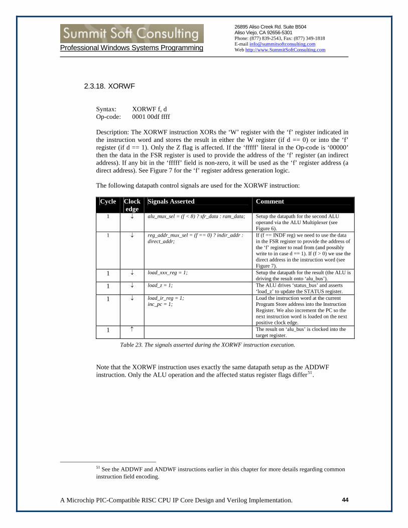
Professional Windows Systems Programming
A Microchip PIC-Compatible RISC CPU IP Core Design and Verilog Implementation. 44
26895 Aliso Creek Rd. Suite B504 Aliso Viejo, CA 92656-5301 Phone: (877) 839-2543, Fax: (877) 349-1818 E-mail [email protected] Web http://www.SummitSoftConsulting.com
2.3.18. XORWF
Syntax: XORWF f, d Op-code: 0001 00df ffff Description: The XORWF instruction XORs the ‘W’ register with the ‘f’ register indicated in the instruction word and stores the result in either the W register (if d == 0) or into the ‘f’ register (if d == 1). Only the Z flag is affected. If the ‘fffff’ literal in the Op-code is ‘00000’ then the data in the FSR register is used to provide the address of the ‘f’ register (an indirect address). If any bit in the ‘fffff’ field is non-zero, it will be used as the ‘f’ register address (a direct address). See Figure 7 for the ‘f’ register address generation logic.
The following datapath control signals are used for the XORWF instruction:
Cycle Clock edge
Signals Asserted Comment
1 ↓ alu_mux_sel = (f < 8) ? sfr_data : ram_data;
Setup the datapath for the second ALU operand via the ALU Multiplexer (see Figure 6).
1 ↓ reg_addr_mux_sel = (f == 0) ? indir_addr : direct_addr;
If (f == INDF reg) we need to use the data in the FSR register to provide the address of the ‘f’ register to read from (and possibly write to in case d == 1). If (f > 0) we use the direct address in the instruction word (see Figure 7).
1 ↓ load_xxx_reg = 1; Setup the datapath for the result (the ALU is driving the result onto ‘alu_bus’).
1 ↓ load_z = 1; The ALU drives ‘status_bus’ and asserts ‘load_z’ to update the STATUS register.
1 ↓ load_ir_reg = 1; inc_pc = 1;
Load the instruction word at the current Program Store address into the Instruction Register. We also increment the PC so the next instruction word is loaded on the next positive clock edge.
1 ↑ The result on ‘alu_bus’ is clocked into the target register.
Table 23. The signals asserted during the XORWF instruction execution.
Note that the XORWF instruction uses exactly the same datapath setup as the ADDWF instruction. Only the ALU operation and the affected status register flags differ51.
51 See the ADDWF and ANDWF instructions earlier in this chapter for more details regarding common instruction field encoding.

Professional Windows Systems Programming
A Microchip PIC-Compatible RISC CPU IP Core Design and Verilog Implementation. 45
26895 Aliso Creek Rd. Suite B504 Aliso Viejo, CA 92656-5301 Phone: (877) 839-2543, Fax: (877) 349-1818 E-mail [email protected] Web http://www.SummitSoftConsulting.com
2.3.19. BCF
Syntax: BCF f, b Op-code: 0100 bbbf ffff Description: The BCF instruction clears bit b of the ‘f’ register indicated in the instruction word and stores the result back into the ‘f’ register. No flags are affected. If the ‘fffff’ literal in the Op-code is ‘00000’ then the data in the FSR register is used to provide the address of the ‘f’ register (an indirect address). If any bit in the ‘fffff’ field is non-zero, it will be used as the ‘f’ register address (a direct address). See Figure 7 for the ‘f’ register address generation logic.
The following datapath control signals are used for the BCF instruction:
Cycle Clock edge
Signals Asserted Comment
1 ↓ alu_mux_sel = (f < 8) ? sfr_data : ram_data;
Setup the datapath for the second ALU operand via the ALU Multiplexer (see Figure 6).
1 ↓ reg_addr_mux_sel = (f == 0) ? indir_addr : direct_addr;
If (f == INDF reg) we need to use the data in the FSR register to provide the address of the ‘f’ register to modify. If (f > 0) we use the direct address in the instruction word (see Figure 7).
1 ↓ load_xxx_reg = 1; Setup the datapath for the result (the ALU is driving the result onto ‘alu_bus’).
1 ↓ load_ir_reg = 1; inc_pc = 1;
Load the instruction word at the current Program Store address into the Instruction Register. We also increment the PC so the next instruction word is loaded on the next positive clock edge.
1 ↑ The result on ‘alu_bus’ is clocked into the target register.
Table 24. The signals asserted during the BCF instruction execution.
Note that the BCF instruction uses exactly the same datapath setup as the ADDWF instruction. Only the ALU operation and the affected status register flags differ52.
52 See the ADDWF and ANDWF instructions earlier in this chapter for more details regarding common instruction field encoding.

Professional Windows Systems Programming
A Microchip PIC-Compatible RISC CPU IP Core Design and Verilog Implementation. 46
26895 Aliso Creek Rd. Suite B504 Aliso Viejo, CA 92656-5301 Phone: (877) 839-2543, Fax: (877) 349-1818 E-mail [email protected] Web http://www.SummitSoftConsulting.com
2.3.20. BSF
Syntax: BSF f, b Op-code: 0101 bbbf ffff Description: The BSF instruction sets bit b of the ‘f’ register indicated in the instruction word and stores the result back into the ‘f’ register. No flags are affected. If the ‘fffff’ literal in the Op-code is ‘00000’ then the data in the FSR register is used to provide the address of the ‘f’ register (an indirect address). If any bit in the ‘fffff’ field is non-zero, it will be used as the ‘f’ register address (a direct address). See Figure 7 for the ‘f’ register address generation logic.
The following datapath control signals are used for the BSF instruction:
Cycle Clock edge
Signals Asserted Comment
1 ↓ alu_mux_sel = (f < 8) ? sfr_data : ram_data;
Setup the datapath for the second ALU operand via the ALU Multiplexer (see Figure 6).
1 ↓ reg_addr_mux_sel = (f == 0) ? indir_addr : direct_addr;
If (f == INDF reg) we need to use the data in the FSR register to provide the address of the ‘f’ register to modify. If (f > 0) we use the direct address in the instruction word (see Figure 7).
1 ↓ load_xxx_reg = 1; Setup the datapath for the result (the ALU is driving the result onto ‘alu_bus’).
1 ↓ load_ir_reg = 1; inc_pc = 1;
Load the instruction word at the current Program Store address into the Instruction Register. We also increment the PC so the next instruction word is loaded on the next positive clock edge.
1 ↑ The result on ‘alu_bus’ is clocked into the target register.
Table 25. The signals asserted during the BSF instruction execution.
Note that the BSF instruction uses exactly the same datapath setup as the ADDWF instruction. Only the ALU operation and the affected status register flags differ53.
53 See the ADDWF and ANDWF instructions earlier in this chapter for more details regarding common instruction field encoding.

Professional Windows Systems Programming
A Microchip PIC-Compatible RISC CPU IP Core Design and Verilog Implementation. 47
26895 Aliso Creek Rd. Suite B504 Aliso Viejo, CA 92656-5301 Phone: (877) 839-2543, Fax: (877) 349-1818 E-mail [email protected] Web http://www.SummitSoftConsulting.com
2.3.21. BTFSC
Syntax: BTFSC f, b Op-code: 0110 bbbf ffff Description: The BTFSC instruction tests if bit b of the ‘f’ register indicated in the instruction word is cleared. If bit b is cleared then the next instruction in the Program Store will be treated as a NOP (i.e. skipped). No flags are affected. If the ‘fffff’ literal in the Op-code is ‘00000’ then the data in the FSR register is used to provide the address of the ‘f’ register (an indirect address). If any bit in the ‘fffff’ field is non-zero, it will be used as the ‘f’ register address (a direct address). See Figure 7 for the ‘f’ register address generation logic.
The following datapath control signals are used for the BTFSC instruction:
Cycle Clock edge
Signals Asserted Comment
1 ↓ alu_mux_sel = (f < 8) ? sfr_data : ram_data;
Setup the datapath for the second ALU operand via the ALU Multiplexer (see Figure 6).
1 ↓ reg_addr_mux_sel = (f == 0) ? indir_addr : direct_addr;
If (f == INDF reg) we need to use the data in the FSR register to provide the address of the ‘f’ register to read from. If (f > 0) we use the direct address in the instruction word (see Figure 7).
1 ↓ load_xxx_reg = 1; Setup the datapath for the result (the ALU is driving the result onto ‘alu_bus’).
1 ↓ load_ir_reg = 1; inc_pc = 1;
Load the instruction word at the current Program Store address into the Instruction Register. We also increment the PC so the next instruction word is loaded on the next positive clock edge.
1 ↑ The result on ‘alu_bus’ is clocked into the target register.
Table 26. The signals asserted during the BTFSC instruction execution.
Note that the BTFSC instruction uses exactly the same datapath setup as the ADDWF instruction. Only the ALU operation and the affected status register flags differ54.
54 See the ADDWF and ANDWF instructions earlier in this chapter for more details regarding common instruction field encoding.
Professional Windows Systems Programming
A Microchip PIC-Compatible RISC CPU IP Core Design and Verilog Implementation. 48
26895 Aliso Creek Rd. Suite B504 Aliso Viejo, CA 92656-5301 Phone: (877) 839-2543, Fax: (877) 349-1818 E-mail [email protected] Web http://www.SummitSoftConsulting.com
2.3.22. BTFSS
Syntax: BTFSS f, b Op-code: 0110 bbbf ffff Description: The BTFSS instruction tests if bit b of the ‘f’ register indicated in the instruction word is set. If bit b is set then the next instruction in the Program Store will be treated as a NOP (i.e. skipped). No flags are affected. If the ‘fffff’ literal in the Op-code is ‘00000’ then the data in the FSR register is used to provide the address of the ‘f’ register (an indirect address). If any bit in the ‘fffff’ field is non-zero, it will be used as the ‘f’ register address (a direct address). See Figure 7 for the ‘f’ register address generation logic.
The following datapath control signals are used for the BTFSS instruction:
Cycle Clock edge
Signals Asserted Comment
1 ↓ alu_mux_sel = (f < 8) ? sfr_data : ram_data;
Setup the datapath for the second ALU operand via the ALU Multiplexer (see Figure 6).
1 ↓ reg_addr_mux_sel = (f == 0) ? indir_addr : direct_addr;
If (f == INDF reg) we need to use the data in the FSR register to provide the address of the ‘f’ register to read from. If (f > 0) we use the direct address in the instruction word (see Figure 7).
1 ↓ load_xxx_reg = 1; Setup the datapath for the result (the ALU is driving the result onto ‘alu_bus’).
1 ↓ load_ir_reg = 1; inc_pc = 1;
Load the instruction word at the current Program Store address into the Instruction Register. We also increment the PC so the next instruction word is loaded on the next positive clock edge.
1 ↑ The result on ‘alu_bus’ is clocked into the target register.
Table 27. The signals asserted during the BTFSS instruction execution.
Note that the BTFSS instruction uses exactly the same datapath setup as the ADDWF instruction. Only the ALU operation and the affected status register flags differ55.
55 See the ADDWF and ANDWF instructions earlier in this chapter for more details regarding common instruction field encoding.

Professional Windows Systems Programming
A Microchip PIC-Compatible RISC CPU IP Core Design and Verilog Implementation. 49
26895 Aliso Creek Rd. Suite B504 Aliso Viejo, CA 92656-5301 Phone: (877) 839-2543, Fax: (877) 349-1818 E-mail [email protected] Web http://www.SummitSoftConsulting.com
2.3.23. ANDLW
Syntax: ANDLW k Op-code: 1110 kkkk kkkk Description: The ANDLW instruction ANDs the ‘W’ register with the literal ‘kkkk kkkk’ encoded in the instruction word. Only the Z flag is affected. The following datapath control signals are used for the ANDLW instruction:
Cycle Clock edge
Signals Asserted Comment
1 ↓ load_w_reg = 1; Setup the datapath for the result (the ALU is driving the result onto ‘alu_bus’).
1 ↓ load_z = 1; The ALU drives ‘status_bus’ and asserts ‘load_z’ to update the STATUS register.
1 ↓ load_ir_reg = 1; inc_pc = 1;
Load the instruction word at the current Program Store address into the Instruction Register. We also increment the PC so the next instruction word is loaded on the next positive clock edge.
1 ↑ The result on ‘alu_bus’ is clocked into the target register.
Table 28. The signals asserted during the ANDLW instruction execution.
Note that the ANDLW instruction uses the ‘W’ register as both source and destination register so no SFR register datapaths need to be set up56.
56 See Fig on page 17. The ALU inputs the source operand from w_reg_bus, ANDs with the literal in ir_reg_bus[7:0] and outputs the result onto alu_bus from where the ‘W’ register loads the result.
ure 6

Professional Windows Systems Programming
A Microchip PIC-Compatible RISC CPU IP Core Design and Verilog Implementation. 50
26895 Aliso Creek Rd. Suite B504 Aliso Viejo, CA 92656-5301 Phone: (877) 839-2543, Fax: (877) 349-1818 E-mail [email protected] Web http://www.SummitSoftConsulting.com
2.3.24. CALL
Syntax: CALL k Op-code: 1001 kkkk kkkk Description: The CALL instruction pushes the address of the next instruction onto the stack and then loads PCL57 with the ‘kkkk kkkk’ literal encoded in the instruction word. This causes the execution to continue at address ‘kkkk kkkk’. No STATUS register flags are affected. This instruction is a 2-cycle instruction.
The following datapath control signals are used for the CALL instruction:
Cycle Clock edge
Signals Asserted Comment
1 ↓ pc_mux_sel = 1; load_pc_reg = 1;
Setup the datapath to load the PC register with the 8-bit call address from 'alu_bus'.
1 ↓ load_stack = 1; Push PC onto the stack.
1 ↓ load_ir_reg = 1; inc_pc = 1;
Load the instruction word at the current Program Store address into the Instruction Register. We also increment the PC so the next instruction word is loaded on the next positive clock edge.
1 ↑ The Program Counter (PC) clocks in the new address to jump to. The PC value is loaded into the current stack location.
2 ↓ load_pc_reg = 0; load_stack = 0;
Deassert the 'load' control signals that were asserted in the first cycle of this instruction.
2 ↓ inc_stack = 1; Increment the current stack location on the second clock cycle.
2 ↑ The main instruction execution loop will at the next rising edge of clock load the IR with the currently addressed instruction word. Since we above updated the PC with the address we should jump to, the IR will be loaded with the target instruction. The execution will therefore continue at the jumped to instruction58.
Table 29. The signals asserted during the CALL instruction execution.
57 PCL is the lowest eight bits of the 9-bit PC register. This means that the CALL instruction can only jump to an absolute address in the first 256-byte memory space. The GOTO instruction must be used to jump to addresses over 255. 58 For detailed information about the implementation of the CALL instruction, see the actual Verilog code in the ‘call’ task in the pic10_controller module in section 3.3.1. pic10_controller.

Professional Windows Systems Programming
A Microchip PIC-Compatible RISC CPU IP Core Design and Verilog Implementation. 51
26895 Aliso Creek Rd. Suite B504 Aliso Viejo, CA 92656-5301 Phone: (877) 839-2543, Fax: (877) 349-1818 E-mail [email protected] Web http://www.SummitSoftConsulting.com
2.3.25. CLRWDT
This instruction is not implemented because the Watchdog Timer register is not implemented.
2.3.26. GOTO
Syntax: GOTO k Op-code: 101k kkkk kkkk Description: The GOTO instruction loads the PC with the ‘k kkkk kkkk’ literal encoded in the instruction word. This causes the execution to continue at address ‘k kkkk kkkk’. No STATUS register flags are affected. This instruction is a 2-cycle instruction.
The following datapath control signals are used for the GOTO instruction:
Cycle Clock edge
Signals Asserted Comment
1 ↓ pc_mux_sel = 2; load_pc_reg = 1;
Setup the datapath to load the PC register with the 9-bit literal from the instruction word.
1 ↓ load_ir_reg = 1; inc_pc = 1;
Load the instruction word at the current Program Store address into the Instruction Register. We also increment the PC so the next instruction word is loaded on the next positive clock edge.
1 ↑ The Program Counter (PC) clocks in the new address.
2 ↓ load_pc_reg = 0; Deassert the 'load' control signals asserted in the first phase of this instruction.
2 ↑ The main instruction execution loop will at the next rising edge of clock load the IR with the currently addressed instruction word. Since we above updated the PC with the address we should jump to, the IR will be loaded with the target instruction. The execution will therefore continue at the jumped to instruction59.
Table 30. The signals asserted during the GOTO instruction execution.
59 For detailed information about the implementation of the GOTO instruction, see the actual Verilog code in the ‘goto’ task in the pic10_controller module in section 3.3.1. pic10_controller.

Professional Windows Systems Programming
A Microchip PIC-Compatible RISC CPU IP Core Design and Verilog Implementation. 52
26895 Aliso Creek Rd. Suite B504 Aliso Viejo, CA 92656-5301 Phone: (877) 839-2543, Fax: (877) 349-1818 E-mail [email protected] Web http://www.SummitSoftConsulting.com
2.3.27. IORLW
Syntax: IORLW k Op-code: 1101 kkkk kkkk Description: The IORLW instruction ORs the ‘W’ register with the literal ‘kkkk kkkk’ encoded in the instruction word. Only the Z flag is affected. The following datapath control signals are used for the IORLW instruction:
Cycle Clock edge
Signals Asserted Comment
1 ↓ load_w_reg = 1; Setup the datapath for the result (the ALU is driving the result onto ‘alu_bus’).
1 ↓ load_z = 1; The ALU drives ‘status_bus’ and asserts ‘load_z’ to update the STATUS register.
1 ↓ load_ir_reg = 1; inc_pc = 1;
Load the instruction word at the current Program Store address into the Instruction Register. We also increment the PC so the next instruction word is loaded on the next positive clock edge.
1 ↑ The result on ‘alu_bus’ is clocked into the target register.
Table 31. The signals asserted during the IORLW instruction execution.
Note that the IORLW instruction uses the ‘W’ register as both source and destination register so no SFR register datapaths need to be set up60. Also note that the datapath setup is identical to the ANDLW instruction.
60 See Fig on page 17. The ALU inputs the source operand from w_reg_bus, ORs with the literal in ir_reg_bus[7:0] and outputs the result onto alu_bus from where the ‘W’ register loads the result.
ure 6

Professional Windows Systems Programming
A Microchip PIC-Compatible RISC CPU IP Core Design and Verilog Implementation. 53
26895 Aliso Creek Rd. Suite B504 Aliso Viejo, CA 92656-5301 Phone: (877) 839-2543, Fax: (877) 349-1818 E-mail [email protected] Web http://www.SummitSoftConsulting.com
2.3.28. MOVLW
Syntax: MOVLW k Op-code: 1100 kkkk kkkk Description: The MOVLW instruction moves the literal ‘kkkk kkkk’ encoded in the instruction word into the ‘W’ register. No status register flag are affected. The following datapath control signals are used for the MOVLW instruction:
Cycle Clock edge
Signals Asserted Comment
1 ↓ load_w_reg = 1; Setup the datapath for the result (the ALU is driving the result onto ‘alu_bus’).
1 ↓ load_ir_reg = 1; inc_pc = 1;
Load the instruction word at the current Program Store address into the Instruction Register. We also increment the PC so the next instruction word is loaded on the next positive clock edge.
1 ↑ The result on ‘alu_bus’ is clocked into the target register.
Table 32. The signals asserted during the MOVLW instruction execution.
Note that the ALU routes the ‘kkkk kkkk’ literal from its ir_reg_bus input to its alu_bus output. The ‘W’ register then loads the data from ‘alu_bus’.
2.3.29. OPTION
This instruction is not implemented because the OPTION register is not implemented.

Professional Windows Systems Programming
A Microchip PIC-Compatible RISC CPU IP Core Design and Verilog Implementation. 54
26895 Aliso Creek Rd. Suite B504 Aliso Viejo, CA 92656-5301 Phone: (877) 839-2543, Fax: (877) 349-1818 E-mail [email protected] Web http://www.SummitSoftConsulting.com
2.3.30. RETLW
Syntax: RETLW k Op-code: 1000 kkkk kkkk Description: This instruction is used to return from a previous function call made via the CALL instruction. The RETLW instruction pops the return address from the stack and loads it into the PCL61 register. The ‘kkkk kkkk’ literal encoded in the instruction word is then loaded into the ‘W’ register62. This causes the execution to continue at the address that was popped from the stack and a return value to be passed back to the calling function. No STATUS register flags are affected. This instruction is a 3-cycle instruction63.
The following datapath control signals are used for the RETLW instruction:
Cycle Clock edge
Signals Asserted Comment
1 ↓ dec_stack = 1; Decrement the stack pointer so the previously stored return address is output on 'pc_bus'.
1 ↓ load_ir_reg = 1; inc_pc = 1;
Load the instruction word at the current Program Store address into the Instruction Register. We also increment the PC so the next instruction word is loaded on the next positive clock edge.
1 ↑ The stack is decremented on the next rising clock edge. This causes the return address to become available on ‘stack_bus’64.
2 ↓ dec_stack = 0; Deassert the dec_stack control signal that was asserted in the first cycle of this instruction.
2 ↓ pc_mux_sel = 0; load_pc_reg = 1;
Load PCL with the previous saved return address on the stack.
2 ↑ The PCL register is loaded with the return address on the next rising edge of clock.
3 ↓ load_pc_reg = 0; Deassert the ‘load_pc_reg’ signal asserted in the previous cycle.
3 ↓ load_ir_reg = 1; load_w_reg = 1;
Load the 'IR' register with the instruction addressed by PC. Load the 'W' register with the 8-bit literal from the RETLW instruction word.
3 ↑ The IR and W registers will be loaded on the next rising clock edge.
Table 33. The signals asserted during the RETLW instruction execution.
61 PCL is the lowest eight bits of the 9-bit PC register. This means that the CALL instruction can only jump to an absolute address in the first 256-byte memory space. The GOTO instruction must be used to jump to addresses over 255. 62 The ‘kkkk kkkk’ literal is used as the return value from the called function. 63 Note that the original Microchip PIC10F20x microcontroller implements the RETLW instruction in two clock cycles. 64 See Fig on page 19. ure 8

Professional Windows Systems Programming
A Microchip PIC-Compatible RISC CPU IP Core Design and Verilog Implementation. 55
26895 Aliso Creek Rd. Suite B504 Aliso Viejo, CA 92656-5301 Phone: (877) 839-2543, Fax: (877) 349-1818 E-mail [email protected] Web http://www.SummitSoftConsulting.com
ted.
2.3.31. SLEEP
This instruction is not implemented because the PIC10 IP Core doesn’t contain any power-management functionality.
2.3.32. TRIS
Syntax: TRIS f Op-code: 0000 0000 0fff Description: The TRIS instruction loads the ‘W’ register into the TRIS register65 with the ‘f’ register address encoded in the instruction word. The TRIS registers 5, 6 or 7 are used to configure the individual bits of I/O ports 5, 6 and 7 as inputs or outputs66. If the ‘fffff’ literal in the Op-code is ‘00000’ then the data in the FSR register is used to provide the address of the ‘f’ register (an indirect address). If any bit in the ‘fffff’ field is non-zero, it will be used as the ‘f’ register address (a direct address). See Figure 7 for the ‘f’ register address generation logic. No status register flag are affec
The following datapath control signals are used for the TRIS instruction:
Cycle Clock edge
Signals Asserted Comment
1 ↓ load_trisx_reg = 1 The ALU outputs the contents of the 'W' register onto 'alu_bus so all we have to do is to assert the correct load_trisx_reg signal67.
1 ↓ load_ir_reg = 1; inc_pc = 1;
Load the instruction word at the current Program Store address into the Instruction Register. We also increment the PC so the next instruction word is loaded on the next positive clock edge.
1 ↑ The result on ‘alu_bus’ is clocked into the target register.
Table 34. The signals asserted during the TRIS instruction execution.
65 See section 2.2.9 Tri-State GPIO Port module (pic10_tri_state_port) on page 22 for more information about the TRIS register implementation. 66 A ‘1’ in the TRIS register configures the corresponding port bit as input. 67 The original Microchip PIC10F20x microcontroller only implements TRIS register 5 while we implement TRIS registers 5, 6 and 7.

Professional Windows Systems Programming
A Microchip PIC-Compatible RISC CPU IP Core Design and Verilog Implementation. 56
26895 Aliso Creek Rd. Suite B504 Aliso Viejo, CA 92656-5301 Phone: (877) 839-2543, Fax: (877) 349-1818 E-mail [email protected] Web http://www.SummitSoftConsulting.com
2.3.33. XORLW Syntax: XORLW k Op-code: 1111 kkkk kkkk Description: The XORLW instruction XORs the ‘W’ register with the literal ‘kkkk kkkk’ encoded in the instruction word. Only the Z flag is affected. The following datapath control signals are used for the XORLW instruction:
Cycle Clock edge
Signals Asserted Comment
1 ↓ load_w_reg = 1; Setup the datapath for the result (the ALU is driving the result onto ‘alu_bus’).
1 ↓ load_z = 1; The ALU drives ‘status_bus’ and asserts ‘load_z’ to update the STATUS register.
1 ↓ load_ir_reg = 1; inc_pc = 1;
Load the instruction word at the current Program Store address into the Instruction Register. We also increment the PC so the next instruction word is loaded on the next positive clock edge.
1 ↑ The result on ‘alu_bus’ is clocked into the target register.
Table 35. The signals asserted during the XORLW instruction execution.
Note that the XORLW instruction uses the ‘W’ register as both source and destination register so no SFR register datapaths need to be set up68. Also note that the datapath setup is identical to the ANDLW instruction.
68 See Fig on page 17. The ALU inputs the source operand from w_reg_bus, XORs with the literal in ir_reg_bus[7:0] and outputs the result onto alu_bus from where the ‘W’ register loads the result.
ure 6

Professional Windows Systems Programming
A Microchip PIC-Compatible RISC CPU IP Core Design and Verilog Implementation. 57
26895 Aliso Creek Rd. Suite B504 Aliso Viejo, CA 92656-5301 Phone: (877) 839-2543, Fax: (877) 349-1818 E-mail [email protected] Web http://www.SummitSoftConsulting.com
3. Appendix A: Verilog Source Code - PIC10 IP Core The following sections list the Verilog source code the PIC10 IP Core. The source code modules are listed in a top-down fashion, starting with the ‘pic10_datapath’ module and ending with the ‘pic10_controller’ module.
3.1. Top-level CPU Verilog Modules (cpu.v)
3.1.1. pic10_cpu
/**************************************************************************** * * By [email protected], 1/17/2007. * * This file contains the top-level 'pic10_cpu' module for the PIC10 RISC Core. * It contains the controller and datapath modules. * The program store is external. * ****************************************************************************/ module pic10_cpu( /////////////////////////////////////////////////////////////// /////////////////////////// Inouts //////////////////////////// /////////////////////////////////////////////////////////////// inout [7:0] gpio5_pin_bus, // Inout: Port 5 pins connected to the outside world. inout [7:0] gpio6_pin_bus, // Inout: Port 6 pins connected to the outside world. inout [7:0] gpio7_pin_bus, // Inout: Port 7 pins connected to the outside world. /////////////////////////////////////////////////////////////// /////////////////////////// Inputs //////////////////////////// /////////////////////////////////////////////////////////////// input reset, // System reset. input clk // System clock. ); /////////////////////////////////////////////////////////////// ///////////////////Internal Wires and buses /////////////////// /////////////////////////////////////////////////////////////// wire zero_result; // Lets the controller know the state of Z-flag // updates so it knows when to increment the PC // during execution of the DECFSZ, INCFSZ, BTFSZ // and BTFSS instructions. wire [4:0] reg_addr_bus; // Used by the controller so it knows which // load_XXX_reg signal to assert when writing to // a register via a direct or indirect address. wire [11:0] ir_reg_bus; // Passes the current instruction code to the // controller so it knows how to direct the // datapath to execute the instruction. wire [8:0] pc_bus; // The program memory address. Will result in // program instructions to be received on the // 'program_bus' bus. wire load_status_reg; // Loads the alu_bus into STATUS register on next // posedge(clk).

Professional Windows Systems Programming
A Microchip PIC-Compatible RISC CPU IP Core Design and Verilog Implementation. 58
26895 Aliso Creek Rd. Suite B504 Aliso Viejo, CA 92656-5301 Phone: (877) 839-2543, Fax: (877) 349-1818 E-mail [email protected] Web http://www.SummitSoftConsulting.com
wire alu_mux_sel; // Selects the 2nd operand to ALU to be // sft_data_bus (0) or ram_data_bus(1). wire load_w_reg; // Loads alu_bus into W register on next // posedge(clk). wire load_fsr_reg; // Loads alu_bus into FSR register on next // posedge(clk). wire load_ram_reg; // Loads alu_bus into the addressed general purpose // register on next posedge(clk). wire reg_addr_mux_sel; // Input: Selects the register address to be used when // reading or writing a register. Can either be a direct // address (0) or an indirect address (1). wire load_tris5_reg; // Used to load the TRIS registers. A '1' in a wire load_tris6_reg; // bit position makes the corresponding bit in wire load_tris7_reg; // the related GPIO register tri-stated (inputs). // The TRIS registers are reset as FFh (inputs). wire load_gpio5_reg; // Used to load the GPIO registers. Output data wire load_gpio6_reg; // is only driven out on the I/O pin if the wire load_gpio7_reg; // corresponding TRIS bit is '0' (output). wire inc_stack; // Increments or decrements the stack pointer on wire dec_stack; // next posedge(clk). wire load_stack; // Loads the current stack location with the // data on the pc_bus (used by the CALL instruction // to store the return address onto the stack). wire load_pc_reg; // loads PC register from pc_mux_bus (used by // the CALL instruction to load the jump address // or used to directly load a new value into PCL // when PCL is used as the target register). wire inc_pc; // Increments the program counter (PC). Used // after instruction fetch as well as in 'skip' // instructions (DECFSZ, INCFSZ, BTFSC and BTFSS). wire [1:0] pc_mux_sel; // Chooses whether the load data to PC should come // from the stack_bus (0), alu_bus (1) or // ir_reg_bus (2). wire load_ir_reg; // Loads IR with the contents of the program // memory word currently being addressed by PC. wire [11:0] program_bus; // Current instruction from the program memory at // the address output at pc_bus. wire skip_next_instruction; ///////////////////////////////////////////////////////////////// // This is the datapath module. ///////////////////////////////////////////////////////////////// pic10_datapath datapath( /////////////////////////// Inouts //////////////////////////// gpio5_pin_bus, // Inout: Port 5 pins connected to the outside world. gpio6_pin_bus, // Inout: Port 6 pins connected to the outside world. gpio7_pin_bus, // Inout: Port 7 pins connected to the outside world. /////////////////////////// Outputs ///////////////////////////

Professional Windows Systems Programming
A Microchip PIC-Compatible RISC CPU IP Core Design and Verilog Implementation. 59
26895 Aliso Creek Rd. Suite B504 Aliso Viejo, CA 92656-5301 Phone: (877) 839-2543, Fax: (877) 349-1818 E-mail [email protected] Web http://www.SummitSoftConsulting.com
zero_result, // Lets the controller know the state of Z-flag // updates so it knows when to increment the PC // during execution of the DECFSZ, INCFSZ, BTFSZ // and BTFSS instructions. reg_addr_bus, // Used by the controller so it knows which // load_XXX_reg signal to assert when writing to // a register via a direct or indirect address. ir_reg_bus, // Passes the current instruction code to the // controller so it knows how to direct the // datapath to execute the instruction. pc_bus, // The program memory address. Will result in // program instructions to be received on the // 'program_bus' bus. /////////////////////////// Inputs //////////////////////////// load_status_reg, // Loads the alu_bus into STATUS register on next // posedge(clk). alu_mux_sel, // Selects the 2nd operand to ALU to be // sft_data_bus (0) or ram_data_bus(1). load_w_reg, // Loads alu_bus into W register on next // posedge(clk). load_fsr_reg, // Loads alu_bus into FSR register on next // posedge(clk). load_ram_reg, // Loads alu_bus into the addressed general purpose // register on next posedge(clk). reg_addr_mux_sel, // Input: Selects the register address to be used when // reading or writing a register. Can either be a direct // address (0) or an indirect address (1). load_tris5_reg, // Used to load the TRIS registers. A '1' in a load_tris6_reg, // bit position makes the corresponding bit in load_tris7_reg, // the related GPIO register tri-stated (inputs). // The TRIS registers are reset as FFh (inputs). load_gpio5_reg, // Used to load the GPIO registers. Output data load_gpio6_reg, // is only driven out on the I/O pin if the load_gpio7_reg, // corresponding TRIS bit is '0' (output). inc_stack, // Increments or decrements the stack pointer on dec_stack, // next posedge(clk). load_stack, // Loads the current stack location with the // data on the pc_bus (used by the CALL instruction // to store the return address onto the stack). load_pc_reg, // loads PC register from pc_mux_bus (used by // the CALL instruction to load the jump address // or used to directly load a new value into PCL // when PCL is used as the target register). inc_pc, // Increments the program counter (PC). Used // after instruction fetch as well as in 'skip' // instructions (DECFSZ, INCFSZ, BTFSC and BTFSS). pc_mux_sel, // Chooses whether the load data to PC should come // from the stack_bus (0), alu_bus (1) or // ir_reg_bus (2).
Professional Windows Systems Programming
A Microchip PIC-Compatible RISC CPU IP Core Design and Verilog Implementation. 60
26895 Aliso Creek Rd. Suite B504 Aliso Viejo, CA 92656-5301 Phone: (877) 839-2543, Fax: (877) 349-1818 E-mail [email protected] Web http://www.SummitSoftConsulting.com
load_ir_reg, // Loads IR with the contents of the program // memory word currently being addressed by PC. program_bus, // Current instruction from the program memory at // the address output at pc_bus. skip_next_instruction, // If the previous instruction was DECFSZ, INCFSZ, // BTFSC or BTFSS and the result was zero we should // not execute the next instruction (i.e. we should // treat the next instruction as a NOP). reset, // System reset. clk); // System clock. ///////////////////////////////////////////////////////////////// // This is the controller module. ///////////////////////////////////////////////////////////////// pic10_controller controller( /////////////////////////// Outputs /////////////////////////// load_status_reg, // Loads the alu_bus into STATUS register on next // posedge(clk). alu_mux_sel, // Selects the 2nd operand to ALU to be // sft_data_bus (0) or ram_data_bus(1). load_w_reg, // Loads alu_bus into W register on next // posedge(clk). load_fsr_reg, // Loads alu_bus into FSR register on next // posedge(clk). load_ram_reg, // Loads alu_bus into the addressed general purpose // register on next posedge(clk). reg_addr_mux_sel, // Selects the register address to be used when reading // or writing a register. Can either be a direct address // (0) or an indirect address (1). load_tris5_reg, // Used to load the TRIS registers. A '1' in a load_tris6_reg, // bit position makes the corresponding bit in load_tris7_reg, // the related GPIO register tri-stated (inputs). // The TRIS registers are reset as FFh (inputs). load_gpio5_reg, // Used to load the GPIO registers. Output data load_gpio6_reg, // is only driven out on the I/O pin if the load_gpio7_reg, // corresponding TRIS bit is '0' (output). inc_stack, // Increments or decrements the stack pointer on dec_stack, // next posedge(clk). load_stack, // Loads the current stack location with the // data on the pc_bus (used by the CALL instruction // to store the return address onto the stack). load_pc_reg, // loads PC register from pc_mux_bus (used by // the CALL instruction to load the jump address // or used to directly load a new value into PCL // when PCL is used as the target register). inc_pc, // Increments the program counter (PC). Used // after instruction fetch as well as in 'skip' // instructions (DECFSZ, INCFSZ, BTFSC and BTFSS). pc_mux_sel[1:0], // Chooses whether the load data to PC should come // from the stack_bus (0), alu_bus (1) or

Professional Windows Systems Programming
A Microchip PIC-Compatible RISC CPU IP Core Design and Verilog Implementation. 61
26895 Aliso Creek Rd. Suite B504 Aliso Viejo, CA 92656-5301 Phone: (877) 839-2543, Fax: (877) 349-1818 E-mail [email protected] Web http://www.SummitSoftConsulting.com
// ir_reg_bus (2). load_ir_reg, // Loads IR with the contents of the program // memory word currently being addressed by PC. skip_next_instruction, // If the previous instruction was DECFSZ, INCFSZ, // BTFSC or BTFSS and the result was zero we should // not execute the next instruction (i.e. we should // treat the next instruction as a NOP). /////////////////////////// Inputs //////////////////////////// zero_result, // Lets the controller know the state of Z-flag // updates so it knows when to increment the PC // during execution of the DECFSZ, INCFSZ, BTFSZ // and BTFSS instructions. reg_addr_bus[4:0], // Used by the controller so it knows which // load_XXX_reg signal to assert when writing to // a register via a direct or indirect address. ir_reg_bus[11:0], // Passes the current instruction code to the // controller so it knows how to direct the // datapath to execute the instruction. reset, // System reset. clk // System clock. ); ///////////////////////////////////////////////////////////////// // This is the program store module. ///////////////////////////////////////////////////////////////// pic10_program_store program_store( /////////////////////////// Outputs /////////////////////////// program_bus[11:0], // Current instruction from the program memory at // the address input at pc_bus. /////////////////////////// Inputs //////////////////////////// pc_bus[8:0], // The program memory address. Will result in // program instructions to be received on the // 'program_bus' bus. ); endmodule
3.2. Datapath Verilog Modules (datapath.v)
3.2.1. pic10_datapath
/**************************************************************************** * * By [email protected], 1/17/2007. * * This file contains all the modules used by the datapath in the PIC10 RISC * CPU core. * * The datapath is software compatible with the PIC10F100 microcontroller

Professional Windows Systems Programming
A Microchip PIC-Compatible RISC CPU IP Core Design and Verilog Implementation. 62
26895 Aliso Creek Rd. Suite B504 Aliso Viejo, CA 92656-5301 Phone: (877) 839-2543, Fax: (877) 349-1818 E-mail [email protected] Web http://www.SummitSoftConsulting.com
* series from Microchip. Note that the datapath is not cycle-accurate * because this implementation is not pipelined in order to keep the imple- * mentation small. The higher clock frequency of a CPLD/FPGA will more than * compensate for this. * * Register differences: TMR0 is not implemented. OSCCAL and CMCON0 registers * have been replaced by two more GPIO registers. PC is 9-bits (no banking * support in the PIC10F100-series so there's no need to implement more bits). * ****************************************************************************/ // These constants determine the signals on the status_bus (output from ALU) // as well as on the status_reg_bus (output from STATUS register). `define STATUS_C 0 `define STATUS_DC 1 `define STATUS_Z 2 // This constant defines the number of stack positions. `define STACK_DEPTH 2 module pic10_datapath( /////////////////////////////////////////////////////////////// /////////////////////////// Inouts //////////////////////////// /////////////////////////////////////////////////////////////// inout [7:0] gpio5_pin_bus, // Inout: Port 5 pins connected to the outside world. inout [7:0] gpio6_pin_bus, // Inout: Port 6 pins connected to the outside world. inout [7:0] gpio7_pin_bus, // Inout: Port 7 pins connected to the outside world. /////////////////////////////////////////////////////////////// /////////////////////////// Outputs /////////////////////////// /////////////////////////////////////////////////////////////// output zero_result, // Lets the controller know the state of Z-flag // updates so it knows when to increment the PC // during execution of the DECFSZ, INCFSZ, BTFSZ // and BTFSS instructions. output [4:0] reg_addr_bus, // Used by the controller so it knows which // load_XXX_reg signal to assert when writing to // a register via a direct or indirect address. output [11:0] ir_reg_bus, // Passes the current instruction code to the // controller so it knows how to direct the // datapath to execute the instruction. output [8:0] pc_bus, // The program memory address. Will result in // program instructions to be received on the // 'program_bus' bus. /////////////////////////////////////////////////////////////// /////////////////////////// Inputs //////////////////////////// /////////////////////////////////////////////////////////////// input load_status_reg, // Loads the alu_bus into STATUS register on next // posedge(clk). input alu_mux_sel, // Selects the 2nd operand to ALU to be // sft_data_bus (0) or ram_data_bus(1). input load_w_reg, // Loads alu_bus into W register on next // posedge(clk). input load_fsr_reg, // Loads alu_bus into FSR register on next // posedge(clk).

Professional Windows Systems Programming
A Microchip PIC-Compatible RISC CPU IP Core Design and Verilog Implementation. 63
26895 Aliso Creek Rd. Suite B504 Aliso Viejo, CA 92656-5301 Phone: (877) 839-2543, Fax: (877) 349-1818 E-mail [email protected] Web http://www.SummitSoftConsulting.com
input load_ram_reg, // Loads alu_bus into the addressed general purpose // register on next posedge(clk). input reg_addr_mux_sel, // Selects the register address to be used when reading or writing a // register. Can either be a direct address (0) or an indirect address (1). input load_tris5_reg, // Used to load the TRIS registers. A '1' in a input load_tris6_reg, // bit position makes the corresponding bit in input load_tris7_reg, // the related GPIO register tri-stated (inputs). // The TRIS registers are reset as FFh (inputs). input load_gpio5_reg, // Used to load the GPIO registers. Output data input load_gpio6_reg, // is only driven out on the I/O pin if the input load_gpio7_reg, // corresponding TRIS bit is '0' (output). input inc_stack, // Increments or decrements the stack pointer on input dec_stack, // next posedge(clk). input load_stack, // Loads the current stack location with the // data on the pc_bus (used by the CALL instruction // to store the return address onto the stack). input load_pc_reg, // loads PC register from pc_mux_bus (used by // the CALL instruction to load the jump address // or used to directly load a new value into PCL // when PCL is used as the target register). input inc_pc, // Increments the program counter (PC). Used // after instruction fetch as well as in 'skip' // instructions (DECFSZ, INCFSZ, BTFSC and BTFSS). input [1:0] pc_mux_sel, // Chooses whether the load data to PC should come // from the stack_bus (0), alu_bus (1) or // ir_reg_bus (2). input load_ir_reg, // Loads IR with the contents of the program // memory word currently being addressed by PC. input [11:0] program_bus, // Current instruction from the program memory at // the address output at pc_bus. input skip_next_instruction,// If the previous instruction was DECFSZ, INCFSZ, // BTFSC or BTFSS and the result was zero we should // not execute the next instruction (i.e. we should // treat the next instruction as a NOP). input reset, // System reset. input clk // System clock. ); /////////////////////////////////////////////////////////////// ///////////////////Internal Wires and buses /////////////////// /////////////////////////////////////////////////////////////// wire [7:0] status_reg_bus; // The output from the STATUS register. wire [7:0] alu_bus; // The output result from the ALU. wire [2:0] alu_status_bus; // The status output from the ALU. wire [7:0] sfr_data_bus; // The output from the SFR Data Mux. wire [7:0] fsr_reg_bus; // The output from the FSR register. wire [7:0] triport5_bus; // The value read from GPIO port 5. wire [7:0] triport6_bus; // The value read from GPIO port 6. wire [7:0] triport7_bus; // The value read from GPIO port 7. wire [7:0] ram_data_bus; // The output from the General Purpose RAM. wire [11:0] program_mux_bus; // The output from the Program Mux.

Professional Windows Systems Programming
A Microchip PIC-Compatible RISC CPU IP Core Design and Verilog Implementation. 64
26895 Aliso Creek Rd. Suite B504 Aliso Viejo, CA 92656-5301 Phone: (877) 839-2543, Fax: (877) 349-1818 E-mail [email protected] Web http://www.SummitSoftConsulting.com
/////////////////////////////////////////////////////////////// /////////////////////// Implementation //////////////////////// /////////////////////////////////////////////////////////////// // The 'zero_result' output is tied to the Z bit in the ALU's status_bus. assign zero_result = alu_status_bus[`STATUS_Z]; // This is the status register. It is loaded from alu_bus. // The ALU can also individually set/clear the Z, C and DC bits. pic10_status_reg status_reg( status_reg_bus[7:0], // Output: The current status is always driven. carry_bit, // Output: The carry bit from the STATUS register. alu_bus[7:0], // Input: Data to be loaded when asserting // 'load_status_reg'. load_status_reg, // Input: Loads alu_bus into register at next // posedge(clk). alu_status_bus[2:0], // Input: Z, C and DC status bits. Driven by ALU. load_z, // Input: Changes Z bit accordingly to alu_status_bus.z. load_c, // Input: Changes C bit accordingly to alu_status_bus.c. load_dc, // Input: Changes DC bit accordingly to alu_status_bus.dc. reset, // System reset. clk); // System clock. // This is the SFR Data Mux. It is used to select one of the SFR registers as // ALUs 2nd operand. Note that there is yet another mux inbetween the SFR Data // Mux and the ALU (the ALU Mux) which selects between the SFR Data and General- // Purpose RAM data outputs. reg [7:0] null_bus = 8'b0; // Used to drive 00h on the not implemented INDF // and TMR0 buses. pic10_sfr_data_mux sfr_data_mux( sfr_data_bus, // Output: Operand data from the special function // registers 0..7. reg_addr_bus[2:0], // Input: This is the currently selected register // address (either a direct address or an indirect // address selected by the Register Address Mux). // The SFR Data Mux only uses the three lowest bits. null_bus[7:0], // Input: INDF returns 00h when read. null_bus[7:0], // Input: TMR0 returns 00h when read (not implemented). pc_bus[7:0], // Input: PCL (the lowest 8 bits of the 9-bit PC). status_reg_bus[7:0], // Input: The STATUS register's output. fsr_reg_bus[7:0], // Input: The FSR register's output. triport5_bus[7:0], // Input: The value read from GPIO port 5. // Replaces OSCCAL register. triport6_bus[7:0], // Input: The value read from GPIO port 6. triport7_bus[7:0]); // Input: The value read from GPIO port 7. // Replaces CMCON0 register. // This is the ALU datapath. It contains the ALU, the ALU MUX that selects ALU // operand data from either the sfr_data_bus or ram_data_bus. In addition, this module // contains the W register. Packaging these modules into the ALU Datapath module makes // the ALU Core easy to test separately. pic10_alu_datapath alu_datapath( alu_bus[7:0], // Output: The output from the ALU. This can either be // an unmodified, passed-through operand (W or register), // a literal (constant) from the instruction word or // the result from an arithmetic or logical operation // or some combination of the W reg, registers and a // literal. alu_status_bus[2:0], // Output: Z, C and DC status bits. Driven by ALU when
// an ALU operation affects any of the flags. The load_XXX // outputs will determine which of the alu_status_bus // signals are valid (and should be loaded into the status // register).

Professional Windows Systems Programming
A Microchip PIC-Compatible RISC CPU IP Core Design and Verilog Implementation. 65
26895 Aliso Creek Rd. Suite B504 Aliso Viejo, CA 92656-5301 Phone: (877) 839-2543, Fax: (877) 349-1818 E-mail [email protected] Web http://www.SummitSoftConsulting.com
load_z, // Output: The alu_status_bus.z bit is valid. load_c, // Output: The alu_status_bus.c bit is valid. load_dc, // Output: The alu_status_bus.dc bit is valid. sfr_data_bus[7:0], // Input: Operand data from the special function // registers 0..7. ram_data_bus[7:0], // Input: Operand data from the general-purpose RAM // registers. ir_reg_bus[11:0], // Input: This is the current instruction loaded into the // instruction register. The ALU uses the 'literal' // operand fields in the instruction word. alu_mux_sel, // Input: Selects the ALU's 2nd operand to be either the // data on the sfr_data_bus (0) or the data on the // ram_data_bus (1). load_w_reg, // Input: Loads the data on the alu_bus into the W // register. carry_bit, // Input: The carry bit from the STATUS register. reset, // System reset. clk); // System clock. // This 12-bit multiplexer allows us to replace the next instruction with a NOP. // It is used by the controller to skip over the next actual instruction when // one of the 'skip'-instructions results in a skip of the next instruction. reg [11:0] nop_bus = 12'h000; pic10_program_mux program_mux( program_mux_bus, // Output: This is the bus that drives the ALUs 2nd // operand. program_bus, // Input: Operand data from the program_bus (currently // addressed instruction). nop_bus, // Input: A NOP instruction Op-code (000h). skip_next_instruction); // Input: When asserted, passes through the NOP Op-code. // This is the SFR datapath. It contains the Instruction Register (IR), the FSR // register, the Register Address Mux as well as the General-purpose RAM registers. // Packaging these modules into the 'SFR Datapath' module allows us to more easily // test the functionality of the direct and indirect addressing modes to access RAM. pic10_sfr_datapath sfr_datapath( fsr_reg_bus[7:0], // Output: Contains the indirect register address in the // FSR register. Used by the controller to determine which // load_XXX_reg signal to assert when writing to a SFR or // general-purpose RAM register. ir_reg_bus[11:0], // Output: Contains the instruction word in the // Instruction Register. Used by the controller to // determine which combinational signals to assert to // execute the instruction. Also used by the ALU which // needs to know the 'literal' constant operands (which // some instructions have encoded as part of the // instruction). ram_data_bus[7:0], // Output: The output from the currently addressed // general-purpose RAM register. The address can either be // a direct or indirect address (determined by the // Register Address Mux). reg_addr_bus[4:0], // Output: This is the currently selected register // address (either a direct address or an indirect address // selected by the Register Address Mux). Note that we // only pass in a part-select of the bus. program_mux_bus[11:0], // Input: Carries the program word to load into the

Professional Windows Systems Programming
A Microchip PIC-Compatible RISC CPU IP Core Design and Verilog Implementation. 66
26895 Aliso Creek Rd. Suite B504 Aliso Viejo, CA 92656-5301 Phone: (877) 839-2543, Fax: (877) 349-1818 E-mail [email protected] Web http://www.SummitSoftConsulting.com
// Instruction Register (IR) when 'load_ir_reg' is // asserted. alu_bus[7:0], // Input: The output from the ALU. Loaded into a register // when one of the load_XXX_reg signals are asserted. load_ir_reg, // Input: Loads alu_bus into IR on the next posedge(clk). load_fsr_reg, // Input: Loads alu_bus into FSR on the next posedge(clk). load_ram_reg, // Input: Loads alu_bus into a General-purpose RAM // register with the address driven on reg_addr_bus. The // data is clocked in on the next posedge(clk). reg_addr_mux_sel, // Input: Selects the register address to be used when // reading or writing a register. Can either be a direct // address (0) or an indirect address (1). reset, // System reset. clk); // System clock. // This is the 'PC Datapath'. It contains the Program Counter (PC), the stack and the // PC Mux which allows the PC to be loaded with data from the stack, alu_bus or // ir_reg_bus buses. By putting these modules into the 'PC Datapath' module we can // test the PC push and pop operations. pic10_pc_datapath pc_datapath( pc_bus[8:0], // Output: Drives the current value in the Program // Counter. alu_bus[7:0], // Input: Used to load register values into PC. ir_reg_bus[8:0], // Input: Used to load literal values (constants in // instructions) into PC. pc_mux_sel[1:0], // Input: Allows the PC to be loaded with data from the // internal stack bus (0), // alu_bus (1) or ir_reg_bus (2). load_pc_reg, // Input: Loads the PC from the input bus currently // selected via pc_mux_sel. inc_pc, // Input: Increments the program counter. inc_stack, // Input: Increments the stack pointer. dec_stack, // Input: Decrements the stack pointer. load_stack, // Input: Loads the stack from the current PC value. reset, // System reset. clk); // System clock. // This is the tri-state register number 5. It combines the GPIO and TRIS register 5. pic10_tri_state_port tri_state_port5( gpio5_pin_bus[7:0], // Inout: This is the port bus connected to the outside // world. triport5_bus[7:0], // Output: The value read from GPIO port 5. Replaces // OSCCAL register. alu_bus[7:0], // Input: Used to load register values into the TRIS or // GPIO port (the register to load is determined by // asserting either the load_tris5_reg or the // load_gpio5_reg signal). load_tris5_reg, // Used to load the TRIS register. load_gpio5_reg, // Used to load the GPIO register. reset, // Input: System reset. clk); // Input: System clock. // This is the tri-state register number 6. It combines the GPIO and TRIS register 6. pic10_tri_state_port tri_state_port6( gpio6_pin_bus[7:0], // Inout: This is the port bus connected to the outside // world. triport6_bus[7:0], // Output: The value read from GPIO port 6. alu_bus[7:0], // Input: Used to load register values into the TRIS or // GPIO port (the register to load is determined by // asserting either the load_tris6_reg or the // load_gpio6_reg signal). load_tris6_reg, // Used to load the TRIS register.

Professional Windows Systems Programming
A Microchip PIC-Compatible RISC CPU IP Core Design and Verilog Implementation. 67
26895 Aliso Creek Rd. Suite B504 Aliso Viejo, CA 92656-5301 Phone: (877) 839-2543, Fax: (877) 349-1818 E-mail [email protected] Web http://www.SummitSoftConsulting.com
load_gpio6_reg, // Used to load the GPIO register. reset, // Input: System reset. clk); // Input: System clock. // This is the tri-state register number 7. It combines the GPIO and TRIS register 7. pic10_tri_state_port tri_state_port7( gpio7_pin_bus[7:0], // Inout: This is the port bus connected to the outside // world. triport7_bus[7:0], // Output: The value read from GPIO port 7. Replaces // CMCON0 register. alu_bus[7:0], // Input: Used to load register values into the TRIS or // GPIO port (the register to load is determined by // asserting either the load_tris7_reg or the // load_gpio7_reg signal). load_tris7_reg, // Used to load the TRIS register. load_gpio7_reg, // Used to load the GPIO register. reset, // Input: System reset. clk); // Input: System clock. endmodule

Professional Windows Systems Programming
A Microchip PIC-Compatible RISC CPU IP Core Design and Verilog Implementation. 68
26895 Aliso Creek Rd. Suite B504 Aliso Viejo, CA 92656-5301 Phone: (877) 839-2543, Fax: (877) 349-1818 E-mail [email protected] Web http://www.SummitSoftConsulting.com
3.2.2. pic10_alu_datapath
///////////////////////////////////////////////////////////////// // module pic10_alu_datapath // Tested OK 2/14/07 with testbench 'test_pic10_alu_datapath'. ///////////////////////////////////////////////////////////////// module pic10_alu_datapath( output [7:0] alu_bus, // Output: The output from the ALU. This can either be // an unmodified, passed-through operand (W or register), // a literal (constant) from the instruction word or // the result from an arithmetic or logical operation // or some combination of the W reg, registers and a // literal. output [2:0] alu_status_bus,// Output: Z, C and DC status bits. Driven by ALU // when an ALU operation affects any of the flags. The // load_XXX outputs will determine which of the // alu_status_bus signals are valid (and should be loaded // into the status register). output load_z, // Output: The alu_status_bus.z bit is valid. output load_c, // Output: The alu_status_bus.c bit is valid. output load_dc, // Output: The alu_status_bus.dc bit is valid. input [7:0]sfr_data_bus,// Input: Operand data from the special function // registers 0..7. input [7:0]ram_data_bus,// Input: Operand data from the general-purpose RAM // registers. input [11:0] ir_reg_bus,// Input: This is the current instruction loaded into the // instruction register. The ALU uses the 'literal' // operand fields in the instruction word. input alu_mux_sel, // Input: Selects the ALU's 2nd operand to be either the // data on the sfr_data_bus (0) or the data on the // ram_data_bus (1). input load_w_reg, // Input: Loads the data on the alu_bus into the W // register. input carry_bit, // Input: The carry bit from the STATUS register. input reset, // System reset. input clk); // System clock. /////////////////////////////////////////////////////////////// ///////////////// Internal Wires and Buses //////////////////// /////////////////////////////////////////////////////////////// wire [7:0] alu_mux_bus; wire [7:0] w_reg_bus; /////////////////////////////////////////////////////////////// /////////////////////// Implementation //////////////////////// /////////////////////////////////////////////////////////////// // This is the ALU Mux that selects the 2nd ALU operand to be either // the SFR or the currently addressed general-purpose RAM register. pic10_alu_mux alu_mux( alu_mux_bus[7:0], // Output: This is the bus that drives the ALUs 2nd // operand. sfr_data_bus[7:0], // Input: Operand data from the special function // registers 0..7. ram_data_bus[7:0], // Input: Operand data from the general-purpose RAM // registers. alu_mux_sel); // Input: Selects the ALU's 2nd operand to be either // the data on the sfr_data_bus (0) or the data on the // ram_data_bus (1).

Professional Windows Systems Programming
A Microchip PIC-Compatible RISC CPU IP Core Design and Verilog Implementation. 69
26895 Aliso Creek Rd. Suite B504 Aliso Viejo, CA 92656-5301 Phone: (877) 839-2543, Fax: (877) 349-1818 E-mail [email protected] Web http://www.SummitSoftConsulting.com
// This is the ALU. pic10_alu alu( alu_bus[7:0], // Output: The output from the ALU. This can either be // an unmodified, passed-through operand (W or register), // a literal (constant) from the instruction word or // the result from an arithmetic or logical operation // or some combination of the W reg, registers and a // literal. load_z, // Output: The ALU will set this signal when the Z bit is // affected by an ALU operation. The Z bit itself is part // of the alu_status_bus. load_c, // Output: The ALU will set this signal when the C bit is // affected by an ALU operation. The C bit itself is part // of the alu_status_bus. load_dc, // Output: The ALU will set this signal when the DC bit // is affected by an ALU operation. The DC bit itself is // part of the alu_status_bus. alu_status_bus[2:0], // Output: The ALU drives the Z, C and/or DC status bits // if affected by the ALU operation input on the // ir_reg_bus input. w_reg_bus[7:0], // Input: The output from the W register. Used as 1st ALU // operand. alu_mux_bus[7:0], // Input: This is the bus that drives the ALUs 2nd // operand. ir_reg_bus[11:0], // Input: The ALU retrieves the opcode and literal // operands from this bus. carry_bit); // Input: The carry bit from the STATUS register. // This is the W register. pic10_w_reg w_reg( w_reg_bus[7:0], // Output: The output from the W register. Used as 1st // ALU operand. alu_bus[7:0], // Input: The output from the ALU. This can either be // an unmodified, passed-through operand (W or register), // a literal (constant) from the instruction word or // the result from an arithmetic or logical operation // or some combination of the W reg, registers and a // literal. load_w_reg, // Input: Loads the data on the alu_bus into the W // register. reset, // System reset. clk); // System clock. endmodule
3.2.3. pic10_sfr_datapath
///////////////////////////////////////////////////////////////// // module pic10_sfr_datapath // Tested OK 1/22/07 with testbench 'test_pic10_sfr_datapath'. ///////////////////////////////////////////////////////////////// module pic10_sfr_datapath( output [7:0] fsr_reg_bus, // Output: Contains the indirect register address in the // FSR register. // Used by the controller to determine which load_XXX_reg // signal to assert when writing to a SFR or general- // purpose RAM register. output [11:0] ir_reg_bus, // Output: Contains the instruction word in the // Instruction Register. // Used by the controller to determine which

Professional Windows Systems Programming
A Microchip PIC-Compatible RISC CPU IP Core Design and Verilog Implementation. 70
26895 Aliso Creek Rd. Suite B504 Aliso Viejo, CA 92656-5301 Phone: (877) 839-2543, Fax: (877) 349-1818 E-mail [email protected] Web http://www.SummitSoftConsulting.com
// combinational signals to assert to execute the // instruction. Also used by the ALU which needs to know // the 'literal' constant operands (which some // instructions have encoded as part of the instruction). output [7:0] ram_data_bus, // Output: The output from the currently addressed // general-purpose RAM register. The address can either be // a direct or indirect address (determined by the // Register Address Mux). output [4:0] reg_addr_bus, // Output: This is the currently selected register // address (either a direct address or an indirect address // selected by the Register Address Mux). Used as select // signal for the SFR Data Mux. The SFR Data Mux selects // the SFR data to be used as the 2nd ALU operand. NOTE // that the 2nd ALU operand is further qualified by the // ALU Mux which selects between the output from the SFR // Data Mux and the output from the General Purpose RAM // Registers. input [11:0] program_mux_bus,// Input: Carries the program word to load into the // Instruction Register (IR) when 'load_ir_reg' is // asserted. input [7:0] alu_bus, // Input: The output from the ALU. Loaded into a register // when one of the load_XXX_reg signals are asserted. input load_ir_reg, // Input: Loads program_mux_bus into IR on the next // posedge(clk). input load_fsr_reg, // Input: Loads alu_bus into FSR on the next posedge(clk). input load_ram_reg, // Input: Loads alu_bus into a General-purpose RAM // register with the address driven on reg_addr_bus. The // data is clocked in on next posedge(clk). input reg_addr_mux_sel, // Input: Selects the register address to be used when // reading or writing a register. Can either be a direct // address (0) or an indirect address (1). input reset, // System reset. input clk); // System clock. /////////////////////////////////////////////////////////////// /////////////////////// Implementation //////////////////////// /////////////////////////////////////////////////////////////// // This is the Instruction Register (IR). It holds the // current instruction while it is being executed. pic10_ir ir( ir_reg_bus[11:0], // Output: Contains the instruction word in the // Instruction Register. program_mux_bus[11:0], // Input: Carries the program word to load into the // Instruction Register (IR) when 'load_ir_reg' is // asserted. load_ir_reg, // Input: Loads program_mux_bus into IR on the next // posedge(clk). reset, // System reset. clk); // System clock. // This is the FSR register. The value loaded into the FSR register is used as the // indirect register address when an instruction reads a register via the INDF // register. pic10_fsr fsr( fsr_reg_bus[7:0], // Output: Contains the indirect register address in the // FSR register. alu_bus[7:0], // Input: The output from the ALU. Loaded into the FSR // register when the load_fsr_reg signals is asserted at

Professional Windows Systems Programming
A Microchip PIC-Compatible RISC CPU IP Core Design and Verilog Implementation. 71
26895 Aliso Creek Rd. Suite B504 Aliso Viejo, CA 92656-5301 Phone: (877) 839-2543, Fax: (877) 349-1818 E-mail [email protected] Web http://www.SummitSoftConsulting.com
// the next posedge(clk). load_fsr_reg, // Input: Loads alu_bus into FSR on the next posedge(clk). reset, // System reset. clk); // System clock. // This is the Register Address Mux. It is used to select between // a direct or indirect address when addressing a register. pic10_register_address_mux register_address_mux( reg_addr_bus[4:0], // Output: This is the currently selected register // address (either a direct address or an indirect address // selected by the Register Address Mux). ir_reg_bus[4:0], // Input: This part-select of the complete instruction // word contains a 'literal' constant specifying the // direct address used to access a register (note: only // for selected data-moving instructions). fsr_reg_bus[4:0], // Input: Contains the indirect register address in the // FSR register. // The indirect address is only used when accessing a // register via the FSR register. reg_addr_mux_sel); // Input: Selects the register address to be used when // reading or writing a register. Can either be a direct // address (0) or an indirect address (1). // This is the General Purpose Registers (RAM). pic10_ram_registers ram_registers( ram_data_bus[7:0], // Output: Always outputs the data in the addressed // register. alu_bus[7:0], // Input: The output from the ALU. Loaded into the // register when the load_ram_reg signal is asserted. load_ram_reg, // Input: Loads alu_bus into a General-purpose RAM // register with the address driven on reg_addr_bus. The // data is clocked in on the next posedge(clk). reg_addr_bus[4:0], // Input: This is the currently selected register address // (either a direct address or an indirect address // selected by the Register Address Mux). Note: The first // RAM register is at address 8 because the Special // Function Registers have addresses 0..7. reset, // System reset. clk); // System clock. endmodule
3.2.4. pic10_pc_datapath
///////////////////////////////////////////////////////////////// // module pic10_pc_datapath // Tested OK 1/27/07 with testbench 'test_pic10_pc_datapath'. ///////////////////////////////////////////////////////////////// module pic10_pc_datapath( output [8:0] pc_bus, // Output: Drives the current value in the Program // Counter. input [7:0] alu_bus, // Input: Used to load register values into PC. input [8:0] ir_reg_bus, // Input: Used to load literal values (constants in // instructions) into PC. input [1:0] pc_mux_sel, // Input: Allows the PC to be loaded with data from // the internal stack bus (0), // alu_bus (1) or ir_reg_bus (2). input load_pc_reg, // Input: Loads the PC from the input bus currently // selected via pc_mux_sel. input inc_pc, // Input: Increments the program counter. input inc_stack, // Input: Increments the stack pointer. input dec_stack, // Input: Decrements the stack pointer. input load_stack, // Input: Loads the stack from the current PC value. input reset, // System reset.

Professional Windows Systems Programming
A Microchip PIC-Compatible RISC CPU IP Core Design and Verilog Implementation. 72
26895 Aliso Creek Rd. Suite B504 Aliso Viejo, CA 92656-5301 Phone: (877) 839-2543, Fax: (877) 349-1818 E-mail [email protected] Web http://www.SummitSoftConsulting.com
input clk); // System clock. /////////////////////////////////////////////////////////////// /////////////////////// Implementation //////////////////////// /////////////////////////////////////////////////////////////// // This is the n-level stack. The default stack depth is 2 but it // can be expended by modifying the 'pic10_stack' module. wire [8:0] stack_bus; pic10_stack stack( stack_bus[8:0], // Output: Current stack location data. pc_bus[8:0], // Input: Data to be loaded when asserting load_stack. load_stack, // Input: Loads the stack from the current PC value. inc_stack, // Input: Increments the current stack location. dec_stack, // Input: Decrements the current stack location. reset, // Input: System reset. clk); // Input: System clock. // This is the PC Mux. It allows the PC to be loaded with data from // either the stack_bus (0), alu_bus (1) or the ir_reg_bus (2). wire [8:0] pc_mux_bus; pic10_pc_mux pc_mux( pc_mux_bus[8:0], // Output: The PC will be loaded from this bus. stack_bus[8:0], // Input: Used to load stacked values into PC. alu_bus[7:0], // Input: Used to load register values into PC. ir_reg_bus[8:0], // Input: Used to load literal values (constants in // instructions) into PC. pc_mux_sel[1:0]); // Input: allows the PC to be loaded with data from the // internal stack bus (0), // alu_bus (1) or ir_reg_bus (2). // This is the program counter. pic10_pc pc( pc_bus[8:0], // Output: Drives the current value in the Program // Counter. pc_mux_bus[8:0], // Input: Data to be loaded into PC when 'load_pc_reg' is // asserted. load_pc_reg, // Input: Loads the PC from the input bus currently // selected via pc_mux_sel. inc_pc, // Input: Increments the program counter. reset, // Input: System reset. clk); // Input: System clock. endmodule
3.2.5. pic10_stack
///////////////////////////////////////////////////////////////// // module pic10_stack // Tested OK 1/27/07 with testbench 'test_pic10_stack'. ///////////////////////////////////////////////////////////////// module pic10_stack( output [8:0] stack_bus, // Output: Current stack location data. input [8:0] pc_bus, // Input: Data to be loaded when asserting load_stack. input load_stack, // Input: Loads the stack from the current PC value. input inc_stack, // Input: Increments the current stack location. input dec_stack, // Input: Decrements the current stack location. input reset, // Input: System reset. input clk); // Input: System clock. /////////////////////////////////////////////////////////////// /////////////////////// Implementation ////////////////////////

Professional Windows Systems Programming
A Microchip PIC-Compatible RISC CPU IP Core Design and Verilog Implementation. 73
26895 Aliso Creek Rd. Suite B504 Aliso Viejo, CA 92656-5301 Phone: (877) 839-2543, Fax: (877) 349-1818 E-mail [email protected] Web http://www.SummitSoftConsulting.com
/////////////////////////////////////////////////////////////// // This is the stack storage. reg [8:0] stack_regs[`STACK_DEPTH]; // This is the internal stack pointer. It is updated // by the inc_stack and dec_stack signals. reg sp; always @(posedge clk) begin if(reset) sp <= 0; else if(load_stack) stack_regs[sp] <= pc_bus; else if(inc_stack) sp <= sp + 1; else if(dec_stack) sp <= sp - 1; end assign stack_bus = stack_regs[sp]; endmodule
3.2.6. pic10_pc_mux
///////////////////////////////////////////////////////////////// // module pic10_pc_mux // Tested OK 1/27/07 with testbench 'test_pic10_pc_mux'. ///////////////////////////////////////////////////////////////// module pic10_pc_mux( output reg [8:0] pc_mux_bus,// Output: The PC will be loaded from this bus. input [8:0] stack_bus, // Input: Used to load stacked values into PC. input [7:0] alu_bus, // Input: Used to load register values into PC. input [8:0] ir_reg_bus, // Input: Used to load literal values (constants // in instructions) into PC. input [1:0] pc_mux_sel); // Input: allows the PC to be loaded with data from // the internal stack bus (0), alu_bus (1) or // ir_reg_bus (2). /////////////////////////////////////////////////////////////// /////////////////////// Implementation //////////////////////// /////////////////////////////////////////////////////////////// reg [8:0] null_bus = 0; always @(stack_bus, alu_bus, ir_reg_bus, pc_mux_sel) begin case(pc_mux_sel) 2'd0: pc_mux_bus = stack_bus; 2'd1: pc_mux_bus = {1'b0, alu_bus}; 2'd2: pc_mux_bus = ir_reg_bus; default: pc_mux_bus = null_bus; endcase end endmodule

Professional Windows Systems Programming
A Microchip PIC-Compatible RISC CPU IP Core Design and Verilog Implementation. 74
26895 Aliso Creek Rd. Suite B504 Aliso Viejo, CA 92656-5301 Phone: (877) 839-2543, Fax: (877) 349-1818 E-mail [email protected] Web http://www.SummitSoftConsulting.com
3.2.7. pic10_pc
///////////////////////////////////////////////////////////////// // module pic10_pc // Tested OK 1/27/07 with testbench 'test_pic10_pc'. ///////////////////////////////////////////////////////////////// module pic10_pc( output reg [8:0] pc_bus, // Output: Drives the current value in the Program // Counter. input [8:0] pc_mux_bus, // Input: Data to be loaded into PC when 'load_pc_reg' // is asserted. input load_pc_reg, // Input: Loads the PC from the input bus currently // selected via pc_mux_sel. input inc_pc, // Input: Increments the program counter. input reset, // Input: System reset. input clk); // Input: System clock. /////////////////////////////////////////////////////////////// /////////////////////// Implementation //////////////////////// /////////////////////////////////////////////////////////////// always @(posedge clk) begin // 'reset' takes precedence over other inputs. if(reset) pc_bus <= 0; else if(load_pc_reg) pc_bus <= pc_mux_bus; else if(inc_pc) pc_bus <= pc_bus + 1; end endmodule
3.2.8. pic10_ir
///////////////////////////////////////////////////////////////// // module pic10_ir // Tested OK 1/27/07 with testbench 'test_pic10_ir'. ///////////////////////////////////////////////////////////////// module pic10_ir( output reg [11:0] ir_reg_bus, // Output: Contains the instruction word in the // Instruction Register. input [11:0] program_mux_bus, // Input: Carries the program word to load into the // Instruction Register // (IR) when 'load_ir_reg' is asserted. input load_ir_reg, // Input: Loads program_mux_bus into IR on the next // posedge(clk). input reset, // Input: System reset. input clk); // Input: System clock. /////////////////////////////////////////////////////////////// /////////////////////// Implementation //////////////////////// /////////////////////////////////////////////////////////////// always @(posedge clk) begin // 'reset' takes precedence over other inputs. if(reset)

Professional Windows Systems Programming
A Microchip PIC-Compatible RISC CPU IP Core Design and Verilog Implementation. 75
26895 Aliso Creek Rd. Suite B504 Aliso Viejo, CA 92656-5301 Phone: (877) 839-2543, Fax: (877) 349-1818 E-mail [email protected] Web http://www.SummitSoftConsulting.com
ir_reg_bus <= 0; else if(load_ir_reg) ir_reg_bus <= program_mux_bus; end endmodule
3.2.9. pic10_fsr
///////////////////////////////////////////////////////////////// // module pic10_fsr // Tested OK 1/27/07 with testbench 'test_pic10_fsr'. ///////////////////////////////////////////////////////////////// module pic10_fsr( output reg [7:0] fsr_reg_bus, // Output: Contains the indirect register address // in the FSR register. input [7:0] alu_bus, // Input: The output from the ALU. Loaded into the FSR // register when the load_fsr_reg signals is asserted at // the next posedge(clk). input load_fsr_reg, // Input: Loads alu_bus into FSR on the next posedge(clk). input reset, // Input: System reset. input clk); // Input: System clock. /////////////////////////////////////////////////////////////// /////////////////////// Implementation //////////////////////// /////////////////////////////////////////////////////////////// always @(posedge clk) begin // 'reset' takes precedence over other inputs. if(reset) fsr_reg_bus <= 0; else if(load_fsr_reg) fsr_reg_bus <= alu_bus; end endmodule
3.2.10. pic10_status_reg
///////////////////////////////////////////////////////////////// // module pic10_status_reg // Tested OK 1/22/07 with testbench 'test_pic10_status_reg'. ///////////////////////////////////////////////////////////////// module pic10_status_reg( output reg [7:0] status_reg_bus,// Output: The current status is always driven. output carry_bit, // Output: The carry bit from the STATUS register. input [7:0] alu_bus, // Input: Data to be loaded when asserting // 'load_status_reg'. input load_status_reg, // Input: Loads alu_bus into register at next // posedge(clk). input [2:0] alu_status_bus, // Input: Z, C and DC status bits. Driven by ALU. input load_z, // Input: Changes Z bit accordingly to // alu_status_bus.z. input load_c, // Input: Changes C bit accordingly to // alu_status_bus.c. input load_dc, // Input: Changes DC bit accordingly to // alu_status_bus.dc.

Professional Windows Systems Programming
A Microchip PIC-Compatible RISC CPU IP Core Design and Verilog Implementation. 76
26895 Aliso Creek Rd. Suite B504 Aliso Viejo, CA 92656-5301 Phone: (877) 839-2543, Fax: (877) 349-1818 E-mail [email protected] Web http://www.SummitSoftConsulting.com
input reset, // Input: System reset. input clk); // Input: System clock. /////////////////////////////////////////////////////////////// /////////////////////// Implementation //////////////////////// /////////////////////////////////////////////////////////////// always @(posedge clk) begin // 'reset' takes precedence over other inputs. if(reset) status_reg_bus <= 0; else begin if(load_status_reg) begin // If ANY of the status bits are being updated by 'status_bus' we do // not allow a write to these bits by the parallel loaded data. if(load_z || load_c || load_dc) status_reg_bus[7:3] <= alu_bus[7:3]; else status_reg_bus <= alu_bus; end if(load_z) status_reg_bus[`STATUS_Z] = alu_status_bus[`STATUS_Z]; if(load_c) status_reg_bus[`STATUS_C] = alu_status_bus[`STATUS_C]; if(load_dc) status_reg_bus[`STATUS_DC] = alu_status_bus[`STATUS_DC]; end end assign carry_bit = status_reg_bus[`STATUS_C]; endmodule
3.2.11. pic10_sfr_data_mux
///////////////////////////////////////////////////////////////// // module pic10_sfr_data_mux // Tested OK 1/22/07 with testbench 'test_pic10_sfr_data_mux'. ///////////////////////////////////////////////////////////////// module pic10_sfr_data_mux( output reg [7:0] sfr_data_bus, // Output: Operand data from the special function // registers 0..7. input [2:0] sfr_data_mux_sel, // Input: This is the currently selected register // address (either a direct address or an indirect // address selected by the Register Address Mux). The // SFR Data Mux only uses the three lowest bits. input [7:0] indf_reg_bus, // Input: The INDF register's output. input [7:0] tmr0_reg_bus, // Input: The TMR0 register's output. input [7:0] pcl_reg_bus, // Input: The PCL register's output (the lowest 8 // bits of the 9-bit PC). input [7:0] status_reg_bus, // Input: The STATUS register's output. input [7:0] fsr_reg_bus, // Input: The FSR register's output. input [7:0] triport5_bus, // Input: The value read from GPIO port 5 (replaces // OSCCAL register). input [7:0] triport6_bus, // Input: The value read from GPIO port 6. input [7:0] triport7_bus); // Input: The value read from GPIO port 7 (replaces // CMCON0 register).

Professional Windows Systems Programming
A Microchip PIC-Compatible RISC CPU IP Core Design and Verilog Implementation. 77
26895 Aliso Creek Rd. Suite B504 Aliso Viejo, CA 92656-5301 Phone: (877) 839-2543, Fax: (877) 349-1818 E-mail [email protected] Web http://www.SummitSoftConsulting.com
/////////////////////////////////////////////////////////////// /////////////////////// Implementation //////////////////////// /////////////////////////////////////////////////////////////// always @(sfr_data_mux_sel, indf_reg_bus, tmr0_reg_bus, pcl_reg_bus, status_reg_bus, fsr_reg_bus, triport5_bus, triport6_bus, triport7_bus) begin case(sfr_data_mux_sel) 3'd0: sfr_data_bus = indf_reg_bus; 3'd1: sfr_data_bus = tmr0_reg_bus; 3'd2: sfr_data_bus = pcl_reg_bus; 3'd3: sfr_data_bus = status_reg_bus; 3'd4: sfr_data_bus = fsr_reg_bus; 3'd5: sfr_data_bus = triport5_bus; 3'd6: sfr_data_bus = triport6_bus; 3'd7: sfr_data_bus = triport7_bus; endcase end endmodule
3.2.12. pic10_register_address_mux
///////////////////////////////////////////////////////////////// // module pic10_register_address_mux // Tested OK 1/22/07 with testbench 'test_pic10_register_address_mux'. ///////////////////////////////////////////////////////////////// module pic10_register_address_mux( output [4:0] reg_addr_bus, // Output: This is the currently selected register // address (either a direct address or an indirect // address selected by the Register Address Mux). input [4:0] ir_reg_bus, // Input: This part-select of the complete // instruction word contains a 'literal' constant // specifying the direct address used to access // a register (note: only for selected data-moving // instructions). input [4:0] fsr_reg_bus, // Input: Contains the indirect register address in // the FSR register. The indirect address is only used // when accessing a register via the FSR register. input reg_addr_mux_sel); // Input: Selects the register address to be used // when reading or writing a register. Can either be a // direct address (0) or an indirect address (1). /////////////////////////////////////////////////////////////// /////////////////////// Implementation //////////////////////// /////////////////////////////////////////////////////////////// assign reg_addr_bus = reg_addr_mux_sel ? fsr_reg_bus : ir_reg_bus; endmodule
3.2.13. pic10_ram_registers
///////////////////////////////////////////////////////////////// // module pic10_ram_registers // Tested OK 1/21/07 with testbench 'test_pic10_ram_registers'. /////////////////////////////////////////////////////////////////

Professional Windows Systems Programming
A Microchip PIC-Compatible RISC CPU IP Core Design and Verilog Implementation. 78
26895 Aliso Creek Rd. Suite B504 Aliso Viejo, CA 92656-5301 Phone: (877) 839-2543, Fax: (877) 349-1818 E-mail [email protected] Web http://www.SummitSoftConsulting.com
module pic10_ram_registers( output [7:0] ram_data_bus, // Output: Always outputs the data in the addressed // register. input [7:0] alu_bus, // Input: The output from the ALU. Loaded into the // register when the load_ram_reg signal is asserted. input load_ram_reg, // Input: Loads alu_bus into a General-purpose RAM // register with the address driven on reg_addr_bus. The // data is clocked in on the next posedge(clk). input [4:0] reg_addr_bus, // Input: This is the currently selected register address // (either a direct address or an indirect address // selected by the Register Address Mux). Note: The first // RAM register is at address 8 because the Special // Function Registers have addresses 0..7. input reset, // Input: System reset. input clk); // Input: System clock. /////////////////////////////////////////////////////////////// /////////////////////// Implementation //////////////////////// /////////////////////////////////////////////////////////////// // This is the RAM register storage (24 8-bit registers). reg [7:0] ram_regs[24]; // This is a loop variable used during reset to initialize the RAM. integer i; always @(posedge clk) begin if(reset) begin // Clear all RAM registers. for(i=0; i<24; i=i+1) ram_regs[i] <= 0; end else if(load_ram_reg) begin ram_regs[reg_addr_bus - 8] <= alu_bus; end end // The RAM registers always output the addressed register. // NOTE: Output 00h for addresses we don't decode (our first // RAM register starts at address 8). // NOTE: Subtract 8 because address 0..7 addresses the SFR registers. assign ram_data_bus = reg_addr_bus >= 5'd8 ? ram_regs[reg_addr_bus - 8] : 0; endmodule
3.2.14. pic10_alu_mux
///////////////////////////////////////////////////////////////// // module pic10_alu_mux // Tested OK 1/20/07 with testbench 'test_pic10_alu_mux'. ///////////////////////////////////////////////////////////////// module pic10_alu_mux( output [7:0] alu_mux_bus, // Output: This is the bus that drives the ALUs 2nd // operand. input [7:0] sfr_data_bus, // Input: Operand data from the special function // registers 0..7. input [7:0] ram_data_bus, // Input: Operand data from the general-purpose RAM // registers. input alu_mux_sel); // Input: Selects the ALU's 2nd operand to be either // the data on the sfr_data_bus (0) or the data on the // ram_data_bus (1).

Professional Windows Systems Programming
A Microchip PIC-Compatible RISC CPU IP Core Design and Verilog Implementation. 79
26895 Aliso Creek Rd. Suite B504 Aliso Viejo, CA 92656-5301 Phone: (877) 839-2543, Fax: (877) 349-1818 E-mail [email protected] Web http://www.SummitSoftConsulting.com
/////////////////////////////////////////////////////////////// /////////////////////// Implementation //////////////////////// /////////////////////////////////////////////////////////////// assign alu_mux_bus = alu_mux_sel ? ram_data_bus : sfr_data_bus; endmodule
3.2.15. pic10_alu
module pic10_alu( output reg [7:0] alu_bus, // Output: The output from the ALU. This can either be // an unmodified, passed-through operand (W or register), // a literal (constant) from the instruction word or // the result from an arithmetic or logical operation // or some combination of the W reg, registers and a // literal. output reg load_z, // Output: The ALU will set this signal when the Z bit // is affected by an ALU operation. The Z bit itself is // part of the alu_status_bus. output reg load_c, // Output: The ALU will set this signal when the C bit is // affected by an ALU operation. The C bit itself is part // of the alu_status_bus. output reg load_dc, // Output: The ALU will set this signal when the DC bit // is affected by an ALU operation. The DC bit itself is // part of the alu_status_bus. output reg [2:0] alu_status_bus,// Output: The ALU drives the Z, C and/or DC status // bits if affected by the ALU operation input on the // ir_reg_bus input. input [7:0] w_reg_bus, // Input: The output from the W register. Used as 1st // ALU operand. input [7:0] alu_mux_bus, // Input: This is the bus that drives the ALUs 2nd // operand. input [11:0] ir_reg_bus, // Input: The ALU retrieves the opcode and literal // operands from this bus. input carry_bit); // Input: The carry bit from the STATUS register. /////////////////////////////////////////////////////////////// /////////////////////// Implementation //////////////////////// /////////////////////////////////////////////////////////////// always @(w_reg_bus, alu_mux_bus, ir_reg_bus, carry_bit) begin // Clear the old status. It will be updated by the below ALU operations. alu_status_bus = 0; load_z = 0; load_c = 0; load_dc = 0; casex(ir_reg_bus) // Mnemonic Operands Description Cycles 12-Bit Opcode Status // Affected // ADDWF f, d Add W and f 1 0001 11df ffff C,DC,Z 12'b0001_11xx_xxxx: addwf(); // ANDWF f, d AND W with f 1 0001 01df ffff Z 12'b0001_01xx_xxxx: andwf(); // CLRF f Clear f 1 0000 011f ffff Z 12'b0000_011x_xxxx: crlf();
Professional Windows Systems Programming
A Microchip PIC-Compatible RISC CPU IP Core Design and Verilog Implementation. 80
26895 Aliso Creek Rd. Suite B504 Aliso Viejo, CA 92656-5301 Phone: (877) 839-2543, Fax: (877) 349-1818 E-mail [email protected] Web http://www.SummitSoftConsulting.com
// CLRW ? Clear W 1 0000 0100 0000 Z 12'b0000_0100_0000: clrw(); // COMF f, d Complement f 1 0010 01df ffff Z 12'b0010_01xx_xxxx: comf(); // MOVWF f Move W to f 1 0000 001f ffff None 12'b0000_001x_xxxx: movwf(); // OPTION ? Load OPTION register 1 0000 0000 0010 None 12'b0000_0000_0010: option(); // DECF f, d Decrement f 1 0000 11df ffff Z 12'b0000_11xx_xxxx: decf(); // DECFSZ f, d Decrement f, Skip if 0 1(2) 0010 11df ffff None 12'b0010_11xx_xxxx: decfsz(); // INCF f, d Increment f 1 0010 10df ffff Z 12'b0010_10xx_xxxx: incf(); // INCFSZ f, d Increment f, Skip if 0 1(2) 0011 11df ffff None 12'b0011_11xx_xxxx: incfsz(); // IORWF f, d Inclusive OR W with f 1 0001 00df ffff Z 12'b0001_00xx_xxxx: iorwf(); // MOVF f, d Move f 1 0010 00df ffff Z 12'b0010_00xx_xxxx: movf(); // NOP ? No Operation 1 0000 0000 0000 None // NOTE: No ALU operation needed. // RLF f, d Rotate left f 1 0011 01df ffff C // through Carry 12'b0011_01xx_xxxx: rlf(); // RRF f, d Rotate right f 1 0011 00df ffff C // through Carry 12'b0011_00xx_xxxx: rrf(); // SUBWF f, d Subtract W from f 1 0000 10df ffff C,DC,Z 12'b0000_10xx_xxxx: subwf(); // SWAPF f, d Swap f 1 0011 10df ffff None 12'b0011_10xx_xxxx: swapf(); // XORWF f, d Exclusive OR W with f 1 0001 10df ffff Z 12'b0001_10xx_xxxx: xorwf(); // BCF f, b Bit Clear f 1 0100 bbbf ffff None 12'b0100_xxxx_xxxx: bcf(); // BSF f, b Bit Set f 1 0101 bbbf ffff None 12'b0101_xxxx_xxxx: bsf(); // BTFSC f, b Bit Test f, 1(2) 0110 bbbf ffff None // Skip if Clear 12'b0110_xxxx_xxxx: bittest(); // NOTE: Common implementation for BTFSC // and BTFSS. // BTFSS f, b Bit Test f, 1(2) 0111 bbbf ffff None // Skip if Set 12'b0111_xxxx_xxxx: bittest(); // NOTE: Common implementation for BTFSC // and BTFSS. // ANDLW k AND literal with W 1 1110 kkkk kkkk Z

Professional Windows Systems Programming
A Microchip PIC-Compatible RISC CPU IP Core Design and Verilog Implementation. 81
26895 Aliso Creek Rd. Suite B504 Aliso Viejo, CA 92656-5301 Phone: (877) 839-2543, Fax: (877) 349-1818 E-mail [email protected] Web http://www.SummitSoftConsulting.com
12'b1110_xxxx_xxxx: andlw(); // CALL k Call Subroutine 2 1001 kkkk kkkk None 12'b1001_xxxx_xxxx: call(); // CLRWDT - Clear Watchdog Timer 1 0000 0000 0100 // NOTE: Not implemented instruction. // GOTO k Unconditional branch 2 101k kkkk kkkk None // NOTE: No ALU operation needed. The controller will // load the 9-bit literal directly from the ir_reg_bus. // IORLW k Inclusive OR literal 1 1101 kkkk kkkk Z // with W 12'b1101_xxxx_xxxx: iorlw(); // MOVLW k Move literal to W 1 1100 kkkk kkkk None 12'b1100_xxxx_xxxx: movlw(); // RETLW k Return, place Literal 2 1000 kkkk kkkk None // in W 12'b1000_xxxx_xxxx: retlw(); // TRIS f Load TRIS register 1 0000 0000 0fff None 3 12'b0000_0000_0101: tris(); // Load TRIS5 12'b0000_0000_0110: tris(); // Load TRIS6 12'b0000_0000_0111: tris(); // Load TRIS7 // SLEEP ? Go into Standby mode 1 0000 0000 0011 // NOTE: Not implemented instruction. // XORLW k Exclusive OR literal 1 1111 kkkk kkkk Z // to W 12'b1111_xxxx_xxxx: xorlw(); endcase end task addwf(); reg 3:0] dummy_result_nybble; [ begin $display("pic10_alu: addwf"); // The controller has already set up the datapath to the operands. // Add the two operands, set the ALU output and update the status bus. // The result and carry flag are calculated in one operation. {alu_status_bus[`STATUS_C], alu_bus} = w_reg_bus + alu_mux_bus; // The Digit Carry (DC) flag reflects a carry from the lower nybble // just like only the lower nybble had been added. {alu_status_bus[`STATUS_DC], dummy_result_nybble} = w_reg_bus[3:0] + alu_mux_bus[3:0]; // The Z flag is set if the result is zero. alu_status_bus[`STATUS_Z] = (alu_bus == 8'b0); // The ADDWF affects all three STATUS register flags. load_z = 1; load_c = 1; load_dc = 1; end endtask task andwf();

Professional Windows Systems Programming
A Microchip PIC-Compatible RISC CPU IP Core Design and Verilog Implementation. 82
26895 Aliso Creek Rd. Suite B504 Aliso Viejo, CA 92656-5301 Phone: (877) 839-2543, Fax: (877) 349-1818 E-mail [email protected] Web http://www.SummitSoftConsulting.com
begin $display("pic10_alu: andwf"); // The controller has already set up the datapath to the operands. // AND the two operands, set the ALU output and update the status bus. // AND the two operands and set the ALU output. alu_bus = w_reg_bus & alu_mux_bus; // Update the status bus. The Z flag is set if the result is zero. alu_status_bus[`STATUS_Z] = (alu_bus == 8'b0); // The ANDWF instruction affects the Z STATUS register flag. load_z = 1; end endtask task crlf(); begin $display("pic10_alu: crlf"); // There are no ALU operands, we simply output 00h. // The controller will load the ALU output into the // 'f' register indicated in the instruction word. alu_bus = 8'b0; // Update the status bus. The Z flag is always set since the result is zero. alu_status_bus[`STATUS_Z] = 1; // The CLRF instruction affects the Z STATUS register flag. load_z = 1; end endtask task clrw(); begin $display("pic10_alu: clrw"); // There are no ALU operands, we simply output 00h. // The controller will load the ALU output into the // 'W' register. alu_bus = 8'b0; // Update the status bus. The Z flag is always set since the result is zero. alu_status_bus[`STATUS_Z] = 1; // The CLRW instruction affects the Z STATUS register flag. load_z = 1; end endtask task comf(); begin $display("pic10_alu: comf"); // The controller has already set up the datapath to the operands. // Complement the 2nd operand, set the ALU output and update the status bus. // Complement the 2nd operand and set the ALU output. alu_bus = ~alu_mux_bus;

Professional Windows Systems Programming
A Microchip PIC-Compatible RISC CPU IP Core Design and Verilog Implementation. 83
26895 Aliso Creek Rd. Suite B504 Aliso Viejo, CA 92656-5301 Phone: (877) 839-2543, Fax: (877) 349-1818 E-mail [email protected] Web http://www.SummitSoftConsulting.com
// Update the status bus. The Z flag is set if the result is zero. alu_status_bus[`STATUS_Z] = (alu_bus == 8'b0); // The COMF instruction affects the Z STATUS register flag. load_z = 1; end endtask task decf(); begin $display("pic10_alu: decf"); // The controller has already set up the datapath to the operands. // Decrement the 2nd operand, set the ALU output and update the status bus. // Decrement the 2nd operand and set the ALU output. alu_bus = alu_mux_bus - 1; // Update the status bus. The Z flag is set if the result is zero. alu_status_bus[`STATUS_Z] = (alu_bus == 8'b0); // The DECF instruction affects the Z STATUS register flag. load_z = 1; end endtask task decfsz(); begin $display("pic10_alu: decfsz"); // The controller has already set up the datapath to the operands. // Decrement the 2nd operand. NOTE that no status flags are updated. // Decrement the 2nd operand and set the ALU output. alu_bus = alu_mux_bus - 1; // Update the status bus. The Z flag is set if the result is zero. // NOTE that the 'load_z' signal is never asserted. The controller // needs to know if we have a zero result in order to skip over the // next instruction. alu_status_bus[`STATUS_Z] = (alu_bus == 8'b0); end endtask task incf(); begin $display("pic10_alu: incf"); // The controller has already set up the datapath to the operands. // Increment the 2nd operand, set the ALU output and update the status bus. // Increment the 2nd operand and set the ALU output. alu_bus = alu_mux_bus + 1; // Update the status bus. The Z flag is set if the result is zero. alu_status_bus[`STATUS_Z] = (alu_bus == 8'b0); // The INCF instruction affects the Z STATUS register flag. load_z = 1; end endtask

Professional Windows Systems Programming
A Microchip PIC-Compatible RISC CPU IP Core Design and Verilog Implementation. 84
26895 Aliso Creek Rd. Suite B504 Aliso Viejo, CA 92656-5301 Phone: (877) 839-2543, Fax: (877) 349-1818 E-mail [email protected] Web http://www.SummitSoftConsulting.com
task incfsz(); begin $display("pic10_alu: incfsz"); // The controller has already set up the datapath to the operands. // Increment the 2nd operand. NOTE that no status flags are updated. // Increment the 2nd operand and set the ALU output. alu_bus = alu_mux_bus + 1; // Update the status bus. The Z flag is set if the result is zero. // NOTE that the 'load_z' signal is never asserted. The controller // needs to know if we have a zero result in order to skip over the // next instruction. alu_status_bus[`STATUS_Z] = (alu_bus == 8'b0); end endtask task iorwf(); begin $display("pic10_alu: iorwf"); // The controller has already set up the datapath to the operands. // OR the two operands, set the ALU output and update the status bus. // OR the two operands and set the ALU output. alu_bus = w_reg_bus | alu_mux_bus; // Update the status bus. The Z flag is set if the result is zero. alu_status_bus[`STATUS_Z] = (alu_bus == 8'b0); // The IORWF instruction affects the Z STATUS register flag. load_z = 1; end endtask task movf(); begin $display("pic10_alu: movf"); // The controller has already set up the datapath to the operands. // Simply pass through the 2nd 'f' operand. alu_bus = alu_mux_bus; // Update the status bus. The Z flag is set if the result is zero. alu_status_bus[`STATUS_Z] = (alu_bus == 8'b0); // The instruction affects the Z STATUS register flag. load_z = 1; end endtask task movwf(); begin $display("pic10_alu: movwf"); // The controller has already set up the datapath to the operands. // Simply pass through the 1st 'W' operand. No flags are affected. alu_bus = w_reg_bus;

Professional Windows Systems Programming
A Microchip PIC-Compatible RISC CPU IP Core Design and Verilog Implementation. 85
26895 Aliso Creek Rd. Suite B504 Aliso Viejo, CA 92656-5301 Phone: (877) 839-2543, Fax: (877) 349-1818 E-mail [email protected] Web http://www.SummitSoftConsulting.com
end endtask task rlf(); begin $display("pic10_alu: rlf"); // The controller has already set up the datapath to the operands. // Rotate the 2nd ALU operand left one bit through the Carry bit. {alu_status_bus[`STATUS_C], alu_bus} = {alu_mux_bus, carry_bit}; // The RLF instruction affects the C STATUS register flag. load_c = 1; end endtask task rrf(); begin $display("pic10_alu: rrf"); // The controller has already set up the datapath to the operands. // Rotate the 2nd ALU operand right one bit through the Carry bit. {alu_bus, alu_status_bus[`STATUS_C]} = {carry_bit, alu_mux_bus}; // The RRF instruction affects the C STATUS register flag. load_c = 1; end endtask task subwf(); begin $display("pic10_alu: subwf"); // The controller has already set up the datapath to the operands. // Subtract W from f, set the ALU output and update the status bus. // Subtract W from f. alu_bus = alu_mux_bus - w_reg_bus; // The Carry flag (C) is cleared if borrow occured. // Borrow occurs (C=0) if the 2nd operand is larger than the 1st operand. // More conveniently, Borrow does not occur (C=1) if the 1st op >= 2nd op. alu_status_bus[`STATUS_C] = alu_mux_bus >= w_reg_bus; // The Digit Carry (DC) flag works the same way as the C flag but it // only deals with the 4 lower bits of the operands and result. alu_status_bus[`STATUS_DC] = alu_mux_bus[3:0] >= w_reg_bus[3:0]; // The Z flag is set if the result is zero. alu_status_bus[`STATUS_Z] = (alu_bus == 8'b0); // The SUBWF instruction affects all three STATUS register flags. load_z = 1; load_c = 1; load_dc = 1; end endtask task swapf(); begin

Professional Windows Systems Programming
A Microchip PIC-Compatible RISC CPU IP Core Design and Verilog Implementation. 86
26895 Aliso Creek Rd. Suite B504 Aliso Viejo, CA 92656-5301 Phone: (877) 839-2543, Fax: (877) 349-1818 E-mail [email protected] Web http://www.SummitSoftConsulting.com
$display("pic10_alu: swapf"); // The controller has already set up the datapath to the operands. // Simply swap the nybbles of 'f', no flags are updated. alu_bus = {alu_mux_bus[3:0], alu_mux_bus[7:4]}; end endtask task xorwf(); begin $display("pic10_alu: xorwf"); // The controller has already set up the datapath to the operands. // XOR the two operands, set the ALU output and update the status bus. // XOR the two operands and set the ALU output. alu_bus = w_reg_bus ^ alu_mux_bus; // Update the status bus. The Z flag is set if the result is zero. alu_status_bus[`STATUS_Z] = (alu_bus == 8'b0); // The XORWF instruction affects the Z STATUS register flag. load_z = 1; end endtask task bcf(); reg [2:0] b; reg [7:0] mask; begin $display("pic10_alu: bcf"); // The controller has already set up the datapath to the operands. // Clear bit 'b' of register 'f', no flags are updated. // The bit index resides in bits [7:5] of the instruction word. b = ir_reg_bus[7:5]; // Create a bit mask with bit 'b' cleared. mask = ~(1<<b); // Clear bit 'b' by AND'ing 'f' with the mask. alu_bus = alu_mux_bus & mask; end endtask task bsf(); reg [2:0] b; reg [7:0] mask; begin $display("pic10_alu: bsf"); // The controller has already set up the datapath to the operands. // Set bit 'b' of register 'f', no flags are updated. // The bit index resides in bits [7:5] of the instruction word. b = ir_reg_bus[7:5]; // Create a bit mask with bit 'b' set. mask = (1<<b); // Set bit 'b' by OR'ing 'f' with the mask.
Professional Windows Systems Programming
A Microchip PIC-Compatible RISC CPU IP Core Design and Verilog Implementation. 87
26895 Aliso Creek Rd. Suite B504 Aliso Viejo, CA 92656-5301 Phone: (877) 839-2543, Fax: (877) 349-1818 E-mail [email protected] Web http://www.SummitSoftConsulting.com
alu_bus = alu_mux_bus | mask; end endtask task bittest(); reg [2:0] b; reg bitset; reg [7:0] mask; begin $display("pic10_alu: bittest"); // The controller has already set up the datapath to the operands. // If bit 'b' of register 'f' is clear we set the Z flag. This // will notify the controller whether the next instruction should be // skipped (i.e. the PC is incremented). // The bit index resides in bits [7:5] of the instruction word. b = ir_reg_bus[7:5]; // Prepare a mask that has the indicated bit set. mask = (1<<b); // Find out if bit 'b' in the 'f' operand is set. bitset = ((alu_mux_bus & mask) == mask); // Update the status bus. NOTE: The Z flag on the bus will NOT be // loaded into the status register (load_z will not be asserted) // but the controller will look at the Z bit to determine whether // the next instruction should be skipped. alu_status_bus[`STATUS_Z] = !bitset; // Drive the ALU bus with arbitrary data (not used). alu_bus = 8'b0; end endtask task andlw(); begin $display("pic10_alu: andlw"); // The controller has already set up the datapath to the operands. // AND 'W' with the literal (constant) in the instruction word, // set the ALU output and update the status bus Z flag. // AND 'W' with the literal (bits [7:0] of the instruction word. alu_bus = w_reg_bus & ir_reg_bus[7:0]; // Update the status bus. The Z flag is set if the result is zero. alu_status_bus[`STATUS_Z] = (alu_bus == 8'b0); // This instruction only affects the Z STATUS register flag. load_z = 1; end endtask task call(); begin $display("pic10_alu: call"); // The controller has already set up the datapath to the operands. // Pass through the 8-bit literal to the output bus. The controller

Professional Windows Systems Programming
A Microchip PIC-Compatible RISC CPU IP Core Design and Verilog Implementation. 88
26895 Aliso Creek Rd. Suite B504 Aliso Viejo, CA 92656-5301 Phone: (877) 839-2543, Fax: (877) 349-1818 E-mail [email protected] Web http://www.SummitSoftConsulting.com
// will load it into the PCL register. alu_bus = ir_reg_bus[7:0]; end endtask task iorlw(); begin $display("pic10_alu: iorlw"); // The controller has already set up the datapath to the operands. // OR 'W' with the literal (constant) in the instruction word, // set the ALU output and update the status bus Z flag. // OR 'W' with the literal (bits [7:0] of the instruction word. alu_bus = w_reg_bus | ir_reg_bus[7:0]; // Update the status bus. The Z flag is set if the result is zero. alu_status_bus[`STATUS_Z] = (alu_bus == 8'b0); // This instruction only affects the Z STATUS register flag. load_z = 1; end endtask task movlw(); begin $display("pic10_alu: movlw"); // The controller has already set up the datapath to the operands. // Pass through the literal to the output. The controller will load // it into the W register. No flags are updated by this instruction. alu_bus = ir_reg_bus[7:0]; end endtask task option(); begin $display("pic10_alu: option"); // The controller has already set up the datapath to the operands. // Pass through the W register to the output. The controller will load // it into the OPTION register. No flags are updated by this instruction. alu_bus = w_reg_bus; end endtask task retlw(); begin $display("pic10_alu: retlw"); // The controller has already set up the datapath to the operands. // Pass through the 8-bit literal to our output bus. The controller // will load the data into the W register. No flags are updated. alu_bus = ir_reg_bus[7:0]; end endtask

Professional Windows Systems Programming
A Microchip PIC-Compatible RISC CPU IP Core Design and Verilog Implementation. 89
26895 Aliso Creek Rd. Suite B504 Aliso Viejo, CA 92656-5301 Phone: (877) 839-2543, Fax: (877) 349-1818 E-mail [email protected] Web http://www.SummitSoftConsulting.com
task tris(); begin $display("pic10_alu: tris"); // The controller has already set up the datapath to the operands. // Pass through the W register to the output. The controller will load // it into the TRIS register. No flags are updated by this instruction. alu_bus = w_reg_bus; end endtask task xorlw(); begin $display("pic10_alu: xorlw"); // The controller has already set up the datapath to the operands. // XOR 'W' with the literal (constant) in the instruction word, // set the ALU output and update the status bus Z flag. // XOR 'W' with the literal (bits [7:0] of the instruction word. alu_bus = w_reg_bus ^ ir_reg_bus[7:0]; // Update the status bus. The Z flag is set if the result is zero. alu_status_bus[`STATUS_Z] = (alu_bus == 8'b0); // This instruction only affects the Z STATUS register flag. load_z = 1; end endtask endmodule
3.2.16. pic10_w_reg
///////////////////////////////////////////////////////////////// // module pic10_w_reg // Tested OK 1/20/07 with testbench 'test_pic10_w_reg'. ///////////////////////////////////////////////////////////////// module pic10_w_reg( output reg [7:0] w_reg_bus, // Output: The output from the W register. // Used as 1st ALU operand. input [7:0] alu_bus, // Input: The output from the ALU. This can either be // an unmodified, passed-through operand (W or register), // a literal (constant) from the instruction word or // the result from an arithmetic or logical operation // or some combination of the W reg, registers and a // literal. input load_w_reg, // Input: Loads the data on the alu_bus into the W // register. input reset, // Input: System reset. input clk); // Input: System clock. /////////////////////// Implementation //////////////////////// always @(posedge clk) begin if(reset) w_reg_bus <= 0;

Professional Windows Systems Programming
A Microchip PIC-Compatible RISC CPU IP Core Design and Verilog Implementation. 90
26895 Aliso Creek Rd. Suite B504 Aliso Viejo, CA 92656-5301 Phone: (877) 839-2543, Fax: (877) 349-1818 E-mail [email protected] Web http://www.SummitSoftConsulting.com
else if (load_w_reg) w_reg_bus <= alu_bus; end endmodule
3.2.17. pic10_tri_state_port
///////////////////////////////////////////////////////////////// // module pic10_tri_state_port // Tested OK 1/20/07 with testbench 'test_pic10_tri_state_port'. ///////////////////////////////////////////////////////////////// module pic10_tri_state_port( inout [7:0] gpio_pin_bus, // Inout: This is the port bus connected to the outside // world. output [7:0] triport_bus, // Output: The value read from GPIO port. Replaces OSCCAL // register. input [7:0] alu_bus, // Input: Used to load register values into the TRIS or // GPIO port (the register to load is determined by // asserting either the load_tris_reg // or the load_gpio_reg signal). input load_tris_reg, // Input: Used to load the TRIS register. input load_gpio_reg, // Input: Used to load the GPIO register. input reset, // Input: System reset. input clk); // Input: System clock. /////////////////////// Implementation //////////////////////// // This is the GPIO and TRIS register storage for this port. reg [7:0] gpio_reg; reg [7:0] tris_reg; always @(posedge clk) begin // We initialize the port as input (FFh) when reset. if(reset) begin gpio_reg <= 8'b0; tris_reg <= 8'hFF; end else if(load_tris_reg) tris_reg <= alu_bus; else if(load_gpio_reg) gpio_reg <= alu_bus; end // These combinational expressions will implement the inout bus. If a TRIS register // bit is '1' then the corresponding port bit will be an input bit. If a TRIS register // bit is '0' then the corresponding GPIO register bit will be driven out on the gpio // port pin. The triport_bus will always reflect the signals on the inout gpio_pin_bus // (either the driven data for output pins or the external data for input pins). assign gpio_pin_bus[7] = tris_reg[7] ? 1'bz : gpio_reg[7]; assign triport_bus[7] = tris_reg[7] ? gpio_pin_bus[7] : gpio_reg[7]; assign gpio_pin_bus[6] = tris_reg[6] ? 1'bz : gpio_reg[6]; assign triport_bus[6] = tris_reg[6] ? gpio_pin_bus[6] : gpio_reg[6]; assign gpio_pin_bus[5] = tris_reg[5] ? 1'bz : gpio_reg[5]; assign triport_bus[5] = tris_reg[5] ? gpio_pin_bus[5] : gpio_reg[5]; assign gpio_pin_bus[4] = tris_reg[4] ? 1'bz : gpio_reg[4]; assign triport_bus[4] = tris_reg[4] ? gpio_pin_bus[4] : gpio_reg[4];

Professional Windows Systems Programming
A Microchip PIC-Compatible RISC CPU IP Core Design and Verilog Implementation. 91
26895 Aliso Creek Rd. Suite B504 Aliso Viejo, CA 92656-5301 Phone: (877) 839-2543, Fax: (877) 349-1818 E-mail [email protected] Web http://www.SummitSoftConsulting.com
assign gpio_pin_bus[3] = tris_reg[3] ? 1'bz : gpio_reg[3]; assign triport_bus[3] = tris_reg[3] ? gpio_pin_bus[3] : gpio_reg[3]; assign gpio_pin_bus[2] = tris_reg[2] ? 1'bz : gpio_reg[2]; assign triport_bus[2] = tris_reg[2] ? gpio_pin_bus[2] : gpio_reg[2]; assign gpio_pin_bus[1] = tris_reg[1] ? 1'bz : gpio_reg[1]; assign triport_bus[1] = tris_reg[1] ? gpio_pin_bus[1] : gpio_reg[1]; assign gpio_pin_bus[0] = tris_reg[0] ? 1'bz : gpio_reg[0]; assign triport_bus[0] = tris_reg[0] ? gpio_pin_bus[0] : gpio_reg[0]; endmodule
3.2.18. pic10_program_mux
///////////////////////////////////////////////////////////////// // module pic10_program_mux ///////////////////////////////////////////////////////////////// module pic10_program_mux( output [11:0] program_mux_bus, // Output: This is the bus that drives the ALUs // 2nd operand. input [11:0] program_bus, // Input: Operand data from the program_bus // (currently addressed instruction). input [11:0] nop_bus, // Input: A NOP instruction Op-code (000h). input program_mux_sel); // Input: When asserted will select the NOP op-code // instead of the real op-code. This is used by the // 'skip' instructions to have the datapath execute // a NOP instead of the actual instruction on the // program bus. /////////////////////////////////////////////////////////////// /////////////////////// Implementation //////////////////////// /////////////////////////////////////////////////////////////// assign program_mux_bus = program_mux_sel ? nop_bus : program_bus; endmodule
3.3. Controller Verilog Modules (controller.v)
3.3.1. pic10_controller
/**************************************************************************** * * By [email protected], 2/26/2007. * * This file contains the controller used in the PIC10 RISC CPU core. * * The controller is software compatible with the PIC10F100 microcontroller * series from Microchip. Note that the controller is not cycle-accurate * because this implementation is not pipelined in order to keep the imple- * mentation small. The higher clock frequency of a CPLD/FPGA will more than * compensate for this. * * Register differences: TMR0 is not implemented. OSCCAL and CMCON0 registers * have been replaced by two more GPIO registers. PC is 9-bits (no banking * support in the PIC10F100-series so there's no need to implement more bits). *

Professional Windows Systems Programming
A Microchip PIC-Compatible RISC CPU IP Core Design and Verilog Implementation. 92
26895 Aliso Creek Rd. Suite B504 Aliso Viejo, CA 92656-5301 Phone: (877) 839-2543, Fax: (877) 349-1818 E-mail [email protected] Web http://www.SummitSoftConsulting.com
****************************************************************************/ module pic10_controller( /////////////////////////////////////////////////////////////// /////////////////////////// Outputs /////////////////////////// /////////////////////////////////////////////////////////////// output reg load_status_reg, // Loads the alu_bus into STATUS register on next // posedge(clk). output wire alu_mux_sel, // Selects the 2nd operand to ALU to be // sft_data_bus (0) or ram_data_bus(1). output reg load_w_reg, // Loads alu_bus into W register on next // posedge(clk). output reg load_fsr_reg, // Loads alu_bus into FSR register on next // posedge(clk). output reg load_ram_reg, // Loads alu_bus into the addressed general purpose // register on next posedge(clk). output wire reg_addr_mux_sel,// Selects the register address to be used when reading // or writing a register. Can either be a direct address // (0) or an indirect address (1). output reg load_tris5_reg, // Used to load the TRIS registers. A '1' in a output reg load_tris6_reg, // bit position makes the corresponding bit in output reg load_tris7_reg, // the related GPIO register tri-stated (inputs). // The TRIS registers are reset as FFh (inputs). output reg load_gpio5_reg, // Used to load the GPIO registers. Output data output reg load_gpio6_reg, // is only driven out on the I/O pin if the output reg load_gpio7_reg, // corresponding TRIS bit is '0' (output). output reg inc_stack, // Increments or decrements the stack pointer on output reg dec_stack, // next posedge(clk). output reg load_stack, // Loads the current stack location with the // data on the pc_bus (used by the CALL instruction // to store the return address onto the stack). output reg load_pc_reg, // loads PC register from pc_mux_bus (used by // the CALL instruction to load the jump address // or used to directly load a new value into PCL // when PCL is used as the target register). output reg inc_pc, // Increments the program counter (PC). Used // after instruction fetch as well as in 'skip' // instructions (DECFSZ, INCFSZ, BTFSC and BTFSS). output reg [1:0] pc_mux_sel,// Chooses whether the load data to PC should come // from the stack_bus (0), alu_bus (1) or // ir_reg_bus (2). output reg load_ir_reg, // Loads IR with the contents of the program // memory word currently being addressed by PC. output reg skip_next_instruction, // If the previous instruction was DECFSZ, INCFSZ, // BTFSC or BTFSS and the result was zero we should // not execute the next instruction (i.e. we should // treat the next instruction as a NOP). /////////////////////////////////////////////////////////////// /////////////////////////// Inputs //////////////////////////// ///////////////////////////////////////////////////////////////
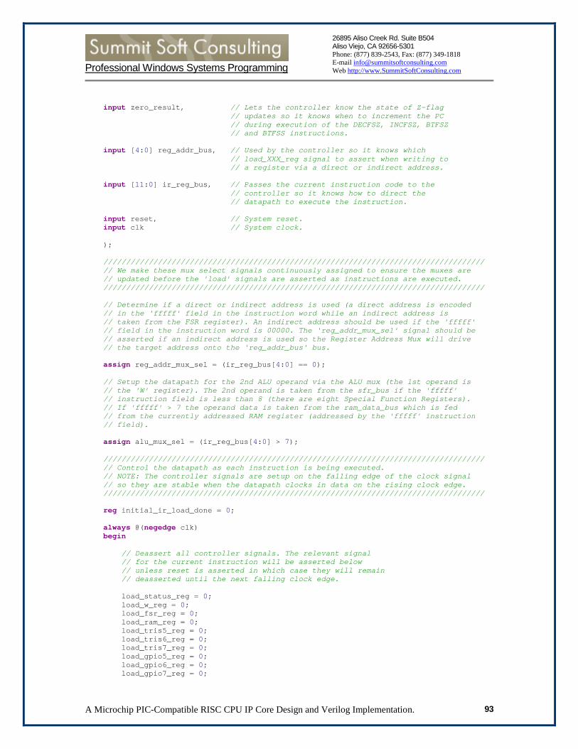
Professional Windows Systems Programming
A Microchip PIC-Compatible RISC CPU IP Core Design and Verilog Implementation. 93
26895 Aliso Creek Rd. Suite B504 Aliso Viejo, CA 92656-5301 Phone: (877) 839-2543, Fax: (877) 349-1818 E-mail [email protected] Web http://www.SummitSoftConsulting.com
input zero_result, // Lets the controller know the state of Z-flag // updates so it knows when to increment the PC // during execution of the DECFSZ, INCFSZ, BTFSZ // and BTFSS instructions. input [4:0] reg_addr_bus, // Used by the controller so it knows which // load_XXX_reg signal to assert when writing to // a register via a direct or indirect address. input [11:0] ir_reg_bus, // Passes the current instruction code to the // controller so it knows how to direct the // datapath to execute the instruction. input reset, // System reset. input clk // System clock. ); //////////////////////////////////////////////////////////////////////////////////// // We make these mux select signals continuously assigned to ensure the muxes are // updated before the 'load' signals are asserted as instructions are executed. //////////////////////////////////////////////////////////////////////////////////// // Determine if a direct or indirect address is used (a direct address is encoded // in the 'fffff' field in the instruction word while an indirect address is // taken from the FSR register). An indirect address should be used if the 'fffff' // field in the instruction word is 00000. The 'reg_addr_mux_sel' signal should be // asserted if an indirect address is used so the Register Address Mux will drive // the target address onto the 'reg_addr_bus' bus. assign reg_addr_mux_sel = (ir_reg_bus[4:0] == 0); // Setup the datapath for the 2nd ALU operand via the ALU mux (the 1st operand is // the 'W' register). The 2nd operand is taken from the sfr_bus if the 'fffff' // instruction field is less than 8 (there are eight Special Function Registers). // If 'fffff' > 7 the operand data is taken from the ram_data_bus which is fed // from the currently addressed RAM register (addressed by the 'fffff' instruction // field). assign alu_mux_sel = (ir_reg_bus[4:0] > 7); //////////////////////////////////////////////////////////////////////////////////// // Control the datapath as each instruction is being executed. // NOTE: The controller signals are setup on the falling edge of the clock signal // so they are stable when the datapath clocks in data on the rising clock edge. //////////////////////////////////////////////////////////////////////////////////// reg initial_ir_load_done = 0; always @(negedge clk) begin // Deassert all controller signals. The relevant signal // for the current instruction will be asserted below // unless reset is asserted in which case they will remain // deasserted until the next falling clock edge. load_status_reg = 0; load_w_reg = 0; load_fsr_reg = 0; load_ram_reg = 0; load_tris5_reg = 0; load_tris6_reg = 0; load_tris7_reg = 0; load_gpio5_reg = 0; load_gpio6_reg = 0; load_gpio7_reg = 0;

Professional Windows Systems Programming
A Microchip PIC-Compatible RISC CPU IP Core Design and Verilog Implementation. 94
26895 Aliso Creek Rd. Suite B504 Aliso Viejo, CA 92656-5301 Phone: (877) 839-2543, Fax: (877) 349-1818 E-mail [email protected] Web http://www.SummitSoftConsulting.com
inc_stack = 0; dec_stack = 0; load_stack = 0; load_pc_reg = 0; inc_pc = 0; pc_mux_sel = 0; load_ir_reg = 0; skip_next_instruction = 0; if(reset == 0 && initial_ir_load_done == 0) begin // Load the instruction word at the current address into the Instruction // Register. NOTE: We also increment the PC so the next instruction word is // loaded while the current instruction is being executed. load_ir_reg = 1; inc_pc = 1; // The initial 'IR' Register load will be done on the next positive edge of // clock. @(posedge clk); initial_ir_load_done = 1; end else begin // Assert the control signals accordingly to the instruction in the // Instruction Register. casex(ir_reg_bus) // Mnemonic Operands Description Cycles 12-Bit Opcode Status Affected // ADDWF f, d Add W and f 1 0001 11df ffff C, DC, Z 12'b0001_11xx_xxxx: addwf(); // ANDWF f, d AND W with f 1 0001 01df ffff Z 12'b0001_01xx_xxxx: andwf(); // CLRF f Clear f 1 0000 011f ffff Z 12'b0000_011x_xxxx: crlf(); // CLRW ? Clear W 1 0000 0100 0000 Z 12'b0000_0100_0000: clrw(); // COMF f, d Complement f 1 0010 01df ffff Z 12'b0010_01xx_xxxx: comf(); // MOVWF f Move W to f 1 0000 001f ffff None 12'b0000_001x_xxxx: movwf(); // OPTION ? Load OPTION register 1 0000 0000 0010 None 12'b0000_0000_0010: option(); // DECF f, d Decrement f 1 0000 11df ffff Z 12'b0000_11xx_xxxx: decf(); // DECFSZ f, d Decrement f, Skip if 0 1(2) 0010 11df ffff None 12'b0010_11xx_xxxx: decfsz(); // INCF f, d Increment f 1 0010 10df ffff Z 12'b0010_10xx_xxxx: incf(); // INCFSZ f, d Increment f, Skip if 0 1(2) 0011 11df ffff None 12'b0011_11xx_xxxx: incfsz(); // IORWF f, d Inclusive OR W with f 1 0001 00df ffff Z 12'b0001_00xx_xxxx: iorwf();
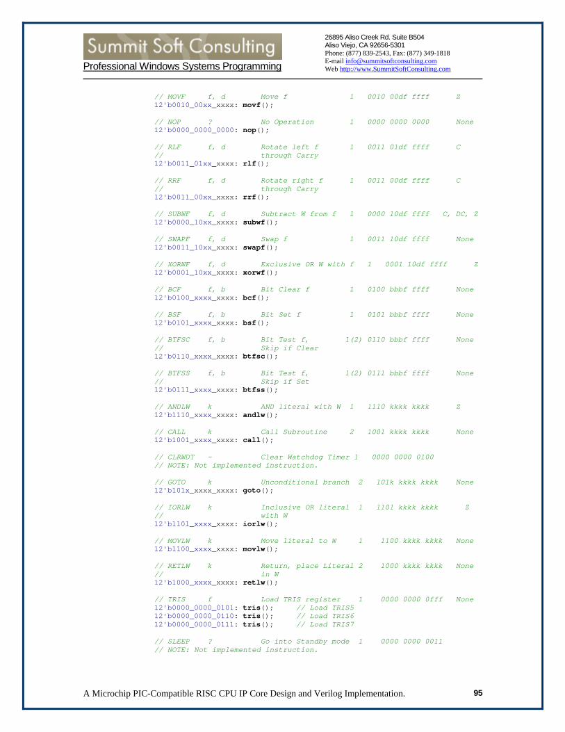
Professional Windows Systems Programming
A Microchip PIC-Compatible RISC CPU IP Core Design and Verilog Implementation. 95
26895 Aliso Creek Rd. Suite B504 Aliso Viejo, CA 92656-5301 Phone: (877) 839-2543, Fax: (877) 349-1818 E-mail [email protected] Web http://www.SummitSoftConsulting.com
// MOVF f, d Move f 1 0010 00df ffff Z 12'b0010_00xx_xxxx: movf(); // NOP ? No Operation 1 0000 0000 0000 None 12'b0000_0000_0000: nop(); // RLF f, d Rotate left f 1 0011 01df ffff C // through Carry 12'b0011_01xx_xxxx: rlf(); // RRF f, d Rotate right f 1 0011 00df ffff C // through Carry 12'b0011_00xx_xxxx: rrf(); // SUBWF f, d Subtract W from f 1 0000 10df ffff C, DC, Z 12'b0000_10xx_xxxx: subwf(); // SWAPF f, d Swap f 1 0011 10df ffff None 12'b0011_10xx_xxxx: swapf(); // XORWF f, d Exclusive OR W with f 1 0001 10df ffff Z 12'b0001_10xx_xxxx: xorwf(); // BCF f, b Bit Clear f 1 0100 bbbf ffff None 12'b0100_xxxx_xxxx: bcf(); // BSF f, b Bit Set f 1 0101 bbbf ffff None 12'b0101_xxxx_xxxx: bsf(); // BTFSC f, b Bit Test f, 1(2) 0110 bbbf ffff None // Skip if Clear 12'b0110_xxxx_xxxx: btfsc(); // BTFSS f, b Bit Test f, 1(2) 0111 bbbf ffff None // Skip if Set 12'b0111_xxxx_xxxx: btfss(); // ANDLW k AND literal with W 1 1110 kkkk kkkk Z 12'b1110_xxxx_xxxx: andlw(); // CALL k Call Subroutine 2 1001 kkkk kkkk None 12'b1001_xxxx_xxxx: call(); // CLRWDT - Clear Watchdog Timer 1 0000 0000 0100 // NOTE: Not implemented instruction. // GOTO k Unconditional branch 2 101k kkkk kkkk None 12'b101x_xxxx_xxxx: goto(); // IORLW k Inclusive OR literal 1 1101 kkkk kkkk Z // with W 12'b1101_xxxx_xxxx: iorlw(); // MOVLW k Move literal to W 1 1100 kkkk kkkk None 12'b1100_xxxx_xxxx: movlw(); // RETLW k Return, place Literal 2 1000 kkkk kkkk None // in W 12'b1000_xxxx_xxxx: retlw(); // TRIS f Load TRIS register 1 0000 0000 0fff None 12'b0000_0000_0101: tris(); // Load TRIS5 12'b0000_0000_0110: tris(); // Load TRIS6 12'b0000_0000_0111: tris(); // Load TRIS7 // SLEEP ? Go into Standby mode 1 0000 0000 0011 // NOTE: Not implemented instruction.

Professional Windows Systems Programming
A Microchip PIC-Compatible RISC CPU IP Core Design and Verilog Implementation. 96
26895 Aliso Creek Rd. Suite B504 Aliso Viejo, CA 92656-5301 Phone: (877) 839-2543, Fax: (877) 349-1818 E-mail [email protected] Web http://www.SummitSoftConsulting.com
// XORLW k Exclusive OR literal 1 1111 kkkk kkkk Z // to W 12'b1111_xxxx_xxxx: xorlw(); endcase // Load the next instruction into IR by asserting the 'load_ir_reg' signal. load_ir_reg = 1; // Increment the PC on the next posedge(clk) by asserting the 'inc_pc' signal. inc_pc = 1; // Wait for the datapath to clock in the data. @(posedge clk); end end task LoadTargetRegister(); begin // The ALU is driving the result of the instruction onto the alu_bus. // We need to assert the correct load_XXX_register to store the result into // either the 'W' register (d == 0), into a SFR (f < 8) or into a RAM Register // (f > 7) by using an indirect address in FSR (f == 0) or into a SFR or // RAM register by using a direct address encoded into the instruction word. // If (d == 0) we store the result back in the 'W' register. if(ir_reg_bus[5] == 0) load_w_reg = 1; else begin // The result should be stored back into an 'f' register. LoadTargetFRegister(); end end endtask task LoadTargetFRegister(); begin // The ALU is driving the result of the instruction onto the alu_bus. // We need to assert the correct load_XXX_register to store the result into // a SFR (f < 8) or into a RAM Register (f > 7) by using an indirect address // in FSR (f == 0) or into a SFR or RAM register by using a direct address // encoded into the instruction word. // Assert the target 'f' register's load signal. case(reg_addr_bus) 5'd0: // INDF. Do Nothing since INDF is not writable. ; 5'd1: // TMR0. Do Nothing since TMR0 is not implemented. ; 5'd2: // PCL. Load PC[7:0] from alu_bus. PC[8] will be cleared. begin pc_mux_sel = 0; load_pc_reg = 1; end 5'd3: // STATUS. Load STATUS register from alu_bus on next posedge(clk). load_status_reg = 1; 5'd4: // FSR. Load FSR register from alu_bus on next posedge(clk). load_fsr_reg = 1; 5'd5: // GPIO5. Load GPIO5 register from alu_bus on next posedge(clk).

Professional Windows Systems Programming
A Microchip PIC-Compatible RISC CPU IP Core Design and Verilog Implementation. 97
26895 Aliso Creek Rd. Suite B504 Aliso Viejo, CA 92656-5301 Phone: (877) 839-2543, Fax: (877) 349-1818 E-mail [email protected] Web http://www.SummitSoftConsulting.com
load_gpio5_reg = 1; 5'd6: // GPIO6. Load GPIO6 register from alu_bus on next posedge(clk). load_gpio6_reg = 1; 5'd7: // GPIO7. Load GPIO7 register from alu_bus on next posedge(clk). load_gpio7_reg = 1; default: // RAM Register. load_ram_reg = 1; endcase end endtask task addwf(); begin //////////////////////////////////////////////////////////////////////////////// // Execute the 'ADDWF f,d' instruction. This instruction adds the content in the // 'W' register with the content of the register indicated by 'f'. The result // goes into the register specified by 'd' in the instruction word (0=>W, 1=>f). // The instruction format is: 0001_11df_ffff. //////////////////////////////////////////////////////////////////////////////// $display("pic10_controller: addwf"); // Load the target register from the alu_bus. LoadTargetRegister(); end endtask task andwf(); begin ///////////////////////////////////////////////////////////////////////////////// // Execute the 'ANDWF f,d' instruction. This instruction ANDs the content in the // 'W' register with the content of the register indicated by 'f'. The result // goes into the register specified by 'd' in the instruction word (0=>W, 1=>f). // The instruction format is: 0001_01df_ffff. ///////////////////////////////////////////////////////////////////////////////// $display("pic10_controller: andwf"); // Load the target register from the alu_bus. LoadTargetRegister(); end endtask task crlf(); begin
/////////////////////////////////////////////////////////////////////////////////
// Execute the 'CLRF f' instruction. This instruction clears the content of the // 'f' register by loading 00h from the alu_bus. // The instruction format is: 0000_011f_ffff.
///////////////////////////////////////////////////////////////////////////////// $display("pic10_controller: crlf"); // Load the target register from the alu_bus. LoadTargetRegister(); end endtask
Professional Windows Systems Programming
A Microchip PIC-Compatible RISC CPU IP Core Design and Verilog Implementation. 98
26895 Aliso Creek Rd. Suite B504 Aliso Viejo, CA 92656-5301 Phone: (877) 839-2543, Fax: (877) 349-1818 E-mail [email protected] Web http://www.SummitSoftConsulting.com
task clrw(); begin
/////////////////////////////////////////////////////////////////////////////////
// Execute the 'CLRW' instruction. This instruction clears the content of the // 'W' register by loading 00h from the alu_bus. // The instruction format is: 0000_0100_0000. ///////////////////////////////////////////////////////////////////////////////// $display("pic10_controller: clrw"); // Load the target register from the alu_bus. LoadTargetRegister(); end endtask task comf(); begin
///////////////////////////////////////////////////////////////////////////////// // COMF f, d: Complements the 'f' register and stores the result in either // the same 'f' register (if d==1) or to the 'W' register (if d==0). // The instruction format is: 0010_01df_ffff.
///////////////////////////////////////////////////////////////////////////////// $display("pic10_controller: comf"); // Load the target register from the alu_bus. LoadTargetRegister(); end endtask task decf(); begin
///////////////////////////////////////////////////////////////////////////////
// DECF f, d: Decrement register 'f' and store result in either // the 'f' register (if d==1) or in the 'W' register (if d==0). // The instruction format is: 0000_11df_ffff. //////////////////////////////////////////////////////////////////////////////// $display("pic10_controller: decf"); // Load the target register from the alu_bus. LoadTargetRegister(); end endtask task decfsz(); begin
/////////////////////////////////////////////////////////////////////////////////
// DECFSZ f, d: Decrement register 'f' and store result in either // the 'f' register (if d==1) or in the 'W' register (if d==0). // Skip the next instruction if the result is 00h. // The instruction format is: 0010 11df ffff.
///////////////////////////////////////////////////////////////////////////////// $display("pic10_controller: decfsz"); // If the result of the DECFSZ instruction // is zero we skip the next instruction.

Professional Windows Systems Programming
A Microchip PIC-Compatible RISC CPU IP Core Design and Verilog Implementation. 99
26895 Aliso Creek Rd. Suite B504 Aliso Viejo, CA 92656-5301 Phone: (877) 839-2543, Fax: (877) 349-1818 E-mail [email protected] Web http://www.SummitSoftConsulting.com
skip_next_instruction = zero_result; // Load the target register from the alu_bus. LoadTargetRegister(); end endtask task incf(); begin
/////////////////////////////////////////////////////////////////////////////////
// INCF f, d: Increment register 'f' and store result in either // the 'f' register (if d==1) or in the 'W' register (if d==0). // The instruction format is: 0010 10df ffff. ///////////////////////////////////////////////////////////////////////////////// $display("pic10_controller: incf"); // Load the target register from the alu_bus. LoadTargetRegister(); end endtask task incfsz(); begin
/////////////////////////////////////////////////////////////////////////////////
// INCFSZ f, d: Increment register 'f' and store the result in either // the 'f' register (if d==1) or in the 'W' register (if d==0). // Skip the next instruction if the result is 00h. // The instruction format is: 0011 11df ffff.
///////////////////////////////////////////////////////////////////////////////// $display("pic10_controller: incfsz"); // If the result of the INCFSZ instruction // is zero we skip the next instruction. skip_next_instruction = zero_result; // Load the target register from the alu_bus. LoadTargetRegister(); end endtask task iorwf(); begin
/////////////////////////////////////////////////////////////////////////////////
// Execute the 'IORWF f,d' instruction. This instruction ORs the content in the // 'W' register with the content of the register indicated by 'f'. The result // goes into the register specified by 'd' in the instruction word (0=>W, 1=>f). // The instruction format is: 0001_00df_ffff. ///////////////////////////////////////////////////////////////////////////////// $display("pic10_controller: iorwf"); // Load the target register from the alu_bus. LoadTargetRegister(); end endtask

Professional Windows Systems Programming
A Microchip PIC-Compatible RISC CPU IP Core Design and Verilog Implementation. 100
26895 Aliso Creek Rd. Suite B504 Aliso Viejo, CA 92656-5301 Phone: (877) 839-2543, Fax: (877) 349-1818 E-mail [email protected] Web http://www.SummitSoftConsulting.com
task movf(); begin
/////////////////////////////////////////////////////////////////////////////////
// Execute the 'MOVF f,d' instruction. This instruction Moves the 'f' register to // either the same 'f' register (if d==1) or to the 'W' register (if d==0). // The instruction format is: 0010_00df_ffff. ///////////////////////////////////////////////////////////////////////////////// $display("pic10_controller: movf"); // Load the target register from the alu_bus. LoadTargetRegister(); end endtask task nop(); begin $display("pic10_controller: nop"); end endtask task movwf(); begin
/////////////////////////////////////////////////////////////////////////////////
// Execute the 'MOVWF f,d' instruction. This instruction Moves the 'W' register // to either an 'f' register (if d==1) or to the 'W' register (if d==0). // The instruction format is: 0000_001f_ffff. ///////////////////////////////////////////////////////////////////////////////// $display("pic10_controller: movf"); // Load the target register from the alu_bus. LoadTargetRegister(); end endtask task rlf(); begin
/////////////////////////////////////////////////////////////////////////////////
// Execute the 'RLF f,d' instruction. This instruction rotates 'f' left through // the carry bit. The result is either stored back to the same 'f' register // (if d==1) or to the 'W' register (if d==0). // The instruction format is: 0011 01df ffff. ///////////////////////////////////////////////////////////////////////////////// $display("pic10_controller: rlf"); // Load the target register from the alu_bus. LoadTargetRegister(); end endtask task rrf(); begin

Professional Windows Systems Programming
A Microchip PIC-Compatible RISC CPU IP Core Design and Verilog Implementation. 101
26895 Aliso Creek Rd. Suite B504 Aliso Viejo, CA 92656-5301 Phone: (877) 839-2543, Fax: (877) 349-1818 E-mail [email protected] Web http://www.SummitSoftConsulting.com
/////////////////////////////////////////////////////////////////////////////////
// Execute the 'RRF f,d' instruction. This instruction rotates 'f' right through // the carry bit. The result is either stored back to the same 'f' register // (if d==1) or to the 'W' register (if d==0). // The instruction format is: 0011 00df ffff. ///////////////////////////////////////////////////////////////////////////////// $display("pic10_controller: rrf"); // Load the target register from the alu_bus. LoadTargetRegister(); end endtask task subwf(); begin
/////////////////////////////////////////////////////////////////////////////////
// Execute the 'SUBWF f,d' instruction. This instruction subtracts 'W' from 'f'. // The result is either stored back to the same 'f' register (if d==1) or to the // 'W' register (if d==0). All flags are affected by this instruction. // The instruction format is: 0000 10df ffff. ///////////////////////////////////////////////////////////////////////////////// $display("pic10_controller: subwf"); // Load the target register from the alu_bus. LoadTargetRegister(); end endtask task swapf(); begin
/////////////////////////////////////////////////////////////////////////////////
// Execute the 'SWAPF f,d' instruction. This instruction swaps the nybbles in 'f'. // The result is either stored back to the same 'f' register (if d==1) or to the // 'W' register (if d==0). No flags are affected by this instruction. // The instruction format is: 0011 10df ffff. ///////////////////////////////////////////////////////////////////////////////// $display("pic10_controller: swapf"); // Load the target register from the alu_bus. LoadTargetRegister(); end endtask task xorwf(); begin
/////////////////////////////////////////////////////////////////////////////////
// Execute the 'XORWF f,d' instruction. This XOR's the 'W' register with the 'f' // register. The result is either stored back to the same 'f' register (if d==1) // or to the 'W' register (if d==0). The 'Z' flag is affected by this instruction. // The instruction format is: 0001 10df ffff. ///////////////////////////////////////////////////////////////////////////////// $display("pic10_controller: xorwf"); // Load the target register from the alu_bus.

Professional Windows Systems Programming
A Microchip PIC-Compatible RISC CPU IP Core Design and Verilog Implementation. 102
26895 Aliso Creek Rd. Suite B504 Aliso Viejo, CA 92656-5301 Phone: (877) 839-2543, Fax: (877) 349-1818 E-mail [email protected] Web http://www.SummitSoftConsulting.com
LoadTargetRegister(); end endtask task bcf(); begin
/////////////////////////////////////////////////////////////////////////////////
// Execute the 'BCF f, b' instruction. This instruction clears bit 'b' in // register 'f'. The result is stored back to the same 'f' register. No flags are // affected. The instruction format is: 0100 bbbf ffff. ///////////////////////////////////////////////////////////////////////////////// $display("pic10_controller: bcf"); // Load the target register from the alu_bus. LoadTargetFRegister(); end endtask task bsf(); begin
//////////////////////////////////////////////////////////////////////////////////
// Execute the 'BSF f, b' instruction. This instruction sets bit 'b' in register // 'f'. The result is stored back to the same 'f' register. No flags are affected. // The instruction format is: 0101 bbbf ffff. ///////////////////////////////////////////////////////////////////////////////// $display("pic10_controller: bsf"); // Load the target register from the alu_bus. LoadTargetFRegister(); end endtask task btfsc(); begin
/////////////////////////////////////////////////////////////////////////////////
// Execute the 'BTFSC f, b' instruction. This instruction tests bit 'b' in // register 'f'. If the bit is clear the next instruction is treated as a NOP. // The instruction format is: 0110 bbbf ffff. ///////////////////////////////////////////////////////////////////////////////// $display("pic10_controller: btfsc"); // If the tested bit is cleared we skip the next instruction. skip_next_instruction = zero_result; // NOTE: No register is modified by this instruction // so we do not assert any load_xxx_reg signal. end endtask task btfss(); begin
/////////////////////////////////////////////////////////////////////////////////
// Execute the 'BTFSS f, b' instruction. This instruction tests bit 'b' in

Professional Windows Systems Programming
A Microchip PIC-Compatible RISC CPU IP Core Design and Verilog Implementation. 103
26895 Aliso Creek Rd. Suite B504 Aliso Viejo, CA 92656-5301 Phone: (877) 839-2543, Fax: (877) 349-1818 E-mail [email protected] Web http://www.SummitSoftConsulting.com
// register 'f'. If the bit is set the next instruction is treated as a NOP. // The instruction format is: 0111 bbbf ffff. ///////////////////////////////////////////////////////////////////////////////// $display("pic10_controller: btfss"); // If the tested bit is set we skip the next instruction. skip_next_instruction = !zero_result; // NOTE: No register is modified by this instruction // so we do not assert any load_xxx_reg signal. end endtask task andlw(); begin
/////////////////////////////////////////////////////////////////////////////////
// Execute the 'ANDLW k' instruction. This instruction ANDs the 'W' register with // the literal 'k' which is encoded in the instruction word. The result is stored // back into the 'W' register. // The instruction format is: 1110 kkkk kkkk. ///////////////////////////////////////////////////////////////////////////////// $display("pic10_controller: andlw"); // The ALU outputs the result on 'alu_bus' so we only need to load // the result of the AND operation back into the 'W' register. load_w_reg = 1; end endtask task call(); begin
/////////////////////////////////////////////////////////////////////////////////
// Execute the 'CALL' instruction. This is a 2-cycle instruction because two // separate tasks need to be done in sequence: 1) The current stack location is // loaded with the current Program Counter (PC) contents. Note that PC contains // the address of THE NEXT instruction to be executed. The PC is then loaded with // the address of the instruction being jumped to. 2) The IR is loaded with the // instruction word addressed by the (newly updated) updated PC. The stack pointer // is also updated in the second clock cycle. // The instruction format is: 1001 kkkk kkkk. ///////////////////////////////////////////////////////////////////////////////// $display("pic10_controller: call"); // Setup the datapath to load the PC register with // the 8-bit call address from the 'alu_bus'. pc_mux_sel = 1; load_pc_reg = 1; // Also push PC onto the stack. load_stack = 1; // Wait for the Program Counter (PC) to clock in the new address to jump to. // The OLD PC value will also be loaded into the current stack location. // NOTE: We continue the controller execution on the NEXT falling edge of clk. // By doing this we have executed a complete cycle in this routine. @(negedge clk); // Deassert the 'load' control signals asserted in the first phase of this // instruction.

Professional Windows Systems Programming
A Microchip PIC-Compatible RISC CPU IP Core Design and Verilog Implementation. 104
26895 Aliso Creek Rd. Suite B504 Aliso Viejo, CA 92656-5301 Phone: (877) 839-2543, Fax: (877) 349-1818 E-mail [email protected] Web http://www.SummitSoftConsulting.com
load_pc_reg = 0; load_stack = 0; // Increment the current stack location on the second clock cycle. inc_stack = 1; // NOTE: The main instruction execution loop will at the next rising edge of // clock load the IR with the currently addressed instruction word. Since we above // updated the PC with the address we should jump to the IR will be loaded with // the instruction being jumped to. The execution will therefore continue at the // jumped to instruction. end endtask task goto(); begin
/////////////////////////////////////////////////////////////////////////////////
// Execute the 'GOTO' instruction. This is a 2-cycle instruction because two // separate tasks need to be done in sequence: 1) The PC is loaded with the // address of the instruction being jumped to. 2) The IR is loaded with the // instruction word addressed by the (newly updated) updated PC. // The instruction format is: 101k kkkk kkkk. ///////////////////////////////////////////////////////////////////////////////// $display("pic10_controller: goto"); // Setup the datapath to load the PC register with // the 9-bit literal from the instruction word. pc_mux_sel = 2; load_pc_reg = 1; // Wait for the Program Counter (PC) to clock in the new address to jump to. // NOTE: We continue the controller execution on the NEXT falling edge of clk. // By doing this we have executed a complete cycle in this routine. @(negedge clk); // Deassert the 'load' control signals asserted in the first phase of this // instruction. load_pc_reg = 0; // NOTE: The main instruction execution loop will at the next rising edge of // clock load the IR with the currently addressed instruction word. Since we above // updated the PC with the address we should jump to the IR will be loaded with // the instruction being jumped to. The execution will therefore continue at the // jumped to instruction. end endtask task iorlw(); begin
/////////////////////////////////////////////////////////////////////////////////
// Execute the 'IORLW k' instruction. This instruction ORs the 'W' register with // the literal 'k' which is encoded in the instruction word. The result is stored // back into the 'W' register. // The instruction format is: 1101 kkkk kkkk. ///////////////////////////////////////////////////////////////////////////////// $display("pic10_controller: iorlw"); // The ALU outputs the result on 'alu_bus' so we only need to load // the result of the AND operation back into the 'W' register. load_w_reg = 1;

Professional Windows Systems Programming
A Microchip PIC-Compatible RISC CPU IP Core Design and Verilog Implementation. 105
26895 Aliso Creek Rd. Suite B504 Aliso Viejo, CA 92656-5301 Phone: (877) 839-2543, Fax: (877) 349-1818 E-mail [email protected] Web http://www.SummitSoftConsulting.com
end endtask task movlw(); begin
/////////////////////////////////////////////////////////////////////////////////
// Execute the 'MOVLW k' instruction. The constant ('literal') to load into the // 'W' Register is encoded in the 8 least significant bits of the instruction. ///////////////////////////////////////////////////////////////////////////////// $display("pic10_controller: movlw"); // The ALU knows (from the instruction word) to pass through the literal to the // alu_bus so all we need to do to load the literal into the 'W' Register is to // assert the load signal. load_w_reg = 1; end endtask task option(); begin $display("pic10_controller: option - NOT IMPLEMENTED"); // NOTE: We don't implement the option register because we currently do not // support any of the features controlled by the option register bits. end endtask task retlw(); begin
/////////////////////////////////////////////////////////////////////////////////
// Execute the "RETLW k" instruction. This instruction is implemented as a 3- // cycle instruction because it needs to perform the following tasks sequencially: // 1) Decrement the stack pointer so the previously stored return address is // output on 'pc_bus'. 2) Load PC with the previous saved return address on the // stack. 3) Load the 'IR' register with the instruction addressed by PC. Load the // 'W' register with the 8-bit literal from the RETLW instruction word. NOTE that // the original PIC CPU implements the RETLW instruction in 2-cycles, likely due // to a more complex stack implementation. It was decided to keep things simple so // we settled for a 3-cycle instruction. The much higher speed of a CPLD/FPGA // implementation more than compensates for the extra execution cycle. ///////////////////////////////////////////////////////////////////////////////// $display("pic10_controller: retlw"); // Cycle 1: Decrement the stack pointer so the previously stored return address // is output on 'pc_bus'. dec_stack = 1; @(negedge clk); // Cycle 2: Load PC with the previous saved return address on the stack. dec_stack = 0; // Deassert - was asserted in Cycle 1. pc_mux_sel = 0; load_pc_reg = 1; @(negedge clk); // Cycle 3: Load the 'IR' register with the instruction addressed by PC. // NOTE: 'load_ir_reg' is asserted by the main always block. // Load the 'W' register with the 8-bit literal from the RETLW instruction word. load_pc_reg = 0; // Deassert - was asserted in Cycle 2.

Professional Windows Systems Programming
A Microchip PIC-Compatible RISC CPU IP Core Design and Verilog Implementation. 106
26895 Aliso Creek Rd. Suite B504 Aliso Viejo, CA 92656-5301 Phone: (877) 839-2543, Fax: (877) 349-1818 E-mail [email protected] Web http://www.SummitSoftConsulting.com
load_w_reg = 1; // NOTE: The main always block will wait until posedge(clk). end endtask task tris(); begin $display("pic10_controller: tris");
//////////////////////////////////////////////////////////////////////////////////
// Execute the 'TRIS f' instruction. The 'W' register is loaded into the TRIS // register indicated by 'f' (where f is 5, 6 or 7). No flags are updated. ///////////////////////////////////////////////////////////////////////////////// // The ALU outputs the contents of the 'W' register onto 'alu_bus // so all we have to do is to assert the correct load_trisX_reg signal. // We get the TRIS register index from bits 2:0 of the instruction word // on the 'ir_reg_bus'. case(ir_reg_bus[2:0]) 3'd5: load_tris5_reg = 1; 3'd6: load_tris6_reg = 1; 7: load_tris7_reg = 1; 3'd endcase end endtask task xorlw(); begin
/////////////////////////////////////////////////////////////////////////////////
// Execute the 'XORLW k' instruction. This instruction XORs the 'W' register with // the literal 'k' which is encoded in the instruction word. The result is stored // back into the 'W' register. // The instruction format is: 1111 kkkk kkkk.
/////////////////////////////////////////////////////////////////////////////////
$display("pic10_controller: xorlw"); // The ALU outputs the result on 'alu_bus' so we only need to load // the result of the AND operation back into the 'W' register. load_w_reg = 1; end endtask endmodule
3.4. Program Store Verilog Modules (program_store.v)
3.4.1. pic10_program_store
/**************************************************************************** * * By [email protected], 2/27/2007. * * This file contains the program store used by the PIC10 RISC CPU core.

Professional Windows Systems Programming
A Microchip PIC-Compatible RISC CPU IP Core Design and Verilog Implementation. 107
26895 Aliso Creek Rd. Suite B504 Aliso Viejo, CA 92656-5301 Phone: (877) 839-2543, Fax: (877) 349-1818 E-mail [email protected] Web http://www.SummitSoftConsulting.com
* ****************************************************************************/ module pic10_program_store( /////////////////////////////////////////////////////////////// /////////////////////////// Outputs /////////////////////////// /////////////////////////////////////////////////////////////// output [11:0] program_bus, // Current instruction from the program memory at // the address input at pc_bus. /////////////////////////////////////////////////////////////// /////////////////////////// Inputs //////////////////////////// /////////////////////////////////////////////////////////////// input [8:0] pc_bus, // The program memory address. Will result in // program instructions to be received on the // 'program_bus' bus. ); //////////////////////////////////////////////////////////////////////////////////// // Hook up the Program Store. //////////////////////////////////////////////////////////////////////////////////// // The encoded instructions are stored here. reg [11:0] ProgramStore [512]; // Wire up the Program Store. assign program_bus = ProgramStore[pc_bus]; // The instructions are stored here in string format. This is so we can display the // current instructions and operands in the Wave window while debugging the code. // We here declare storage for 512 20-byte strings. reg [20*7:0] ProgramStoreText [512]; //////////////////////////////////////////////////////////////////////////////////// // Initialize the program store with instructions to be executed. //////////////////////////////////////////////////////////////////////////////////// initial begin // Address 000h: Load an operand into the 'W' Register with the MOVLW Instruction. ProgramStore[0] = 12'b1100_0100_0100; // C44h. Format 1100_kkkk_kkkk. ProgramStoreText[0] = "MOVLW 44h"; // Address 001h: Move the 'W' register into an 'f' register with the "MOVWF f" // instruction. This is needed so that we later can add the 'W' register with the // 'f' register. We choose to use 'f' register 8 which is the first RAM register. // NOTE that we are using a direct address to address the target register. ProgramStore[1] = 12'b0000_0010_1000; // 028h. Format 0000_001f_ffff. ProgramStoreText[1] = "MOVWF 8h"; // Address 002h: ADDWF: Add the 'W' register (data: 44h) with 'f' register 8 // (data: 44h) NOTE: The 'd' and 'fffff' fields determine the source and // destination registers. We store the result (88h) in the 'W' register since // d == 0. ProgramStore[2] = 12'b0001_1100_1000; // 1C8h. Format 0001_11df_ffff. ProgramStoreText[2] = "ADDWF 8, d"; // Address 004h: NOP. No 'load' signals should be asserted. ProgramStore[3] = 12'b000_0000_0000; ProgramStoreText[3] = "NOP"; // Address 004h: ANDWF: AND the 'W' register (data: 88h) with 'f' register 8 // (data: 44h). NOTE: The 'd' and 'fffff' fields determine the source and // destination registers. We store the result (00h) in the 'W' register since // d == 0.

Professional Windows Systems Programming
A Microchip PIC-Compatible RISC CPU IP Core Design and Verilog Implementation. 108
26895 Aliso Creek Rd. Suite B504 Aliso Viejo, CA 92656-5301 Phone: (877) 839-2543, Fax: (877) 349-1818 E-mail [email protected] Web http://www.SummitSoftConsulting.com
ProgramStore[4] = 12'b0001_0100_1000; // 148h. Format 0001_01df_ffff. ProgramStoreText[4] = "ANDWF 8, d"; // Address 005h: IORWF: OR the 'W' register (data: 00h) with 'f' register 8 // (data: 44h). NOTE: The 'd' and 'fffff' fields determine the source and // destination registers. // We store the result (44h) in the 'W' register since d == 0. ProgramStore[5] = 12'b0001_0000_1000; // 108h. Format 0001_00df_ffff. ProgramStoreText[5] = "IORWF 8, d"; // Address 006h: CLRF: Clear the 'f' register (data: 44h => 00h). ProgramStore[6] = 12'b0000_0110_1000; // 068h. Format 0000 011f ffff. ProgramStoreText[6] = "CLRF 8"; // Address 007h: MOVF f, d: Moves the 'f' register (data: 00h) to // either the same 'f' register (if d==1) or to the 'W' register // (if d==0). We move f=>W. 'W' should change from 44h to 00h. ProgramStore[7] = 12'b0010_0000_1000; // 208h. Format 0010_00df_ffff. ProgramStoreText[7] = "MOVF 8, d"; // Address 008h: COMF f, d: Complements the 'f' register 4 (data: 00h) and // stores the result in either the same 'f' register (if d==1) or to the // 'W' register (if d==0). We here store the result in 'W'. 'W' should // change from 00h to FFh since 'f' register number 4 is cleared (never // touched since reset). Note that 'f' register 4 is the FSR register. ProgramStore[8] = 12'b0010_0100_0100; // 244h. Format 0010_01df_ffff. ProgramStoreText[8] = "COMF 4, d"; // Address 009h: CLRW: Clears the 'W' register (FFh => 00h) ProgramStore[9] = 12'b0000_0100_0000; // 040h. Format 0000_0100_0000. ProgramStoreText[9] = "CLRW"; // Address 00Ah: DECF f, d: Decrement register 'f' and store result in // either the 'f' register (d==1) or in the 'W' register (d==0). We // here decrement the FSR register ('f' register 4) and store the result // back into the FSR register. FSR should change from 00h to ffh. ProgramStore[12'h00A] = 12'b0000_1110_0100; // 0E4h. Format 0000_11df_ffff. ProgramStoreText[12'h00A] = "DECF FSR, f"; //////////////////////////////////////////////////////////////////////////// // Test code to validate the incf instruction. // These instructions loads 01h into 'f' register 8 and then decrements the // register. Since the result is 00h the "MOVLW 55h" should be skipped over and // the "MOVLW AAh" instruction should instead be executed. //////////////////////////////////////////////////////////////////////////// ProgramStore[12'h00B] = 12'b1100_0000_0001; // C01h. Format: 1100 kkkk kkkk. ProgramStoreText[12'h00B] = "MOVLW 1"; ProgramStore[12'h00C] = 12'b0000_0010_1000; // 028h. Format: 0000 001f ffff ProgramStoreText[12'h00C] = "MOVWF 8"; ProgramStore[12'h00D] = 12'b0010_1110_1000; // 1E8h. Format: 0010 11df ffff ProgramStoreText[12'h00D] = "DECFSZ 8, f"; ProgramStore[12'h00E] = 12'b1100_0101_0101; // C55h. Format: 1100 kkkk kkkk. ProgramStoreText[12'h00E] = "MOVLW 55h"; ProgramStore[12'h00F] = 12'b1100_1010_1010; // CAAh. Format: 1100 kkkk kkkk. ProgramStoreText[12'h00F] = "MOVLW AAh";
/////////////////////////////////////////////////////////////////////////////////
// Test code to validate the INCF instruction. // These instructions loads FFh into 'f' register 4 (FSR) and then increments the // register. The resulting FSE should be 00h and the Z flag should be set in the // STATUS register. /////////////////////////////////////////////////////////////////////////////////

Professional Windows Systems Programming
A Microchip PIC-Compatible RISC CPU IP Core Design and Verilog Implementation. 109
26895 Aliso Creek Rd. Suite B504 Aliso Viejo, CA 92656-5301 Phone: (877) 839-2543, Fax: (877) 349-1818 E-mail [email protected] Web http://www.SummitSoftConsulting.com
ProgramStore[12'h010] = 12'b1100_1111_1111; // CFFh. Format: 1100 kkkk kkkk. ProgramStoreText[12'h010] = "MOVLW FF"; ProgramStore[12'h011] = 12'b0000_0010_0100; // 024h. Format: 0000 001f ffff ProgramStoreText[12'h011] = "MOVWF 4"; ProgramStore[12'h012] = 12'b0010_1010_0100; // 2A4h. Format: 0010 10df ffff ProgramStoreText[12'h012] = "INCF 4, f"; /////////////////////////////////////////////////////////////////////////////////
// Test code to validate the INCFSZ instruction. // These instructions loads FFh into 'f' register 31 and then increments the // register. Since the result is 00h the "MOVLW 55h" should be skipped over and // the "MOVLW AAh" instruction should instead be executed. ///////////////////////////////////////////////////////////////////////////////// ProgramStore[12'h013] = 12'b1100_1111_1111; // C01h. Format: 1100 kkkk kkkk. ProgramStoreText[12'h013] = "MOVLW FFh"; ProgramStore[12'h014] = 12'b0000_0011_1111; // 03Fh. Format: 0000 001f ffff ProgramStoreText[12'h014] = "MOVWF 1Fh"; ProgramStore[12'h015] = 12'b0011_1111_1111; // 3FFh. Format: 0011 11df ffff ProgramStoreText[12'h015] = "INCFSZ 1Fh, f"; ProgramStore[12'h016] = 12'b1100_0101_0101; // C55h. Format: 1100 kkkk kkkk. ProgramStoreText[12'h016] = "MOVLW 55h"; ProgramStore[12'h017] = 12'b1100_1010_1010; // CAAh. Format: 1100 kkkk kkkk. ProgramStoreText[12'h017] = "MOVLW AAh"; ///////////////////////////////////////////////////////////////////////////////// // Test code to validate the RLF instruction (Rotate Left 'f' through carry). // These instructions load 80h into 'f' register A and rotates it left twice. // Register A should contain 00h with Carry set after the first RLF instruction. // Register A should contain 01h with Carry clear after the second RLF // instruction. ///////////////////////////////////////////////////////////////////////////////// ProgramStore[12'h018] = 12'b1100_1000_0000; // C80h. Format: 1100 kkkk kkkk. ProgramStoreText[12'h018] = "MOVLW 80h"; ProgramStore[12'h019] = 12'b0000_0010_1010; // 02Ah. Format: 0000 001f ffff ProgramStoreText[12'h019] = "MOVWF Ah"; ProgramStore[12'h01A] = 12'b0011_0110_1010; // 36Ah. Format: 0011 01df ffff ProgramStoreText[12'h01A] = "RLF Ah, f"; // 'f' register A should contain 00h, // C should be set. ProgramStore[12'h01B] = 12'b0011_0110_1010; // 36Ah. Format: 0011 01df ffff ProgramStoreText[12'h01B] = "RLF Ah, f"; // 'f' register A should contain 01h, // C should be clear. ///////////////////////////////////////////////////////////////////////////////// // Test code to validate the RRF instruction (Rotate Right 'f' through carry). // These instructions load 01h into 'f' register A and rotates it right twice. // Register A should contain 00h with Carry set after the first RRF instruction. // Register A should contain 10h with Carry clear after the second RRF // instruction. ///////////////////////////////////////////////////////////////////////////////// ProgramStore[12'h01C] = 12'b1100_0000_0001; // C01h. Format: 1100 kkkk kkkk. ProgramStoreText[12'h01C] = "MOVLW 01h"; ProgramStore[12'h01D] = 12'b0000_0010_1010; // 02Ah. Format: 0000 001f ffff

Professional Windows Systems Programming
A Microchip PIC-Compatible RISC CPU IP Core Design and Verilog Implementation. 110
26895 Aliso Creek Rd. Suite B504 Aliso Viejo, CA 92656-5301 Phone: (877) 839-2543, Fax: (877) 349-1818 E-mail [email protected] Web http://www.SummitSoftConsulting.com
ProgramStoreText[12'h01D] = "MOVWF Ah"; ProgramStore[12'h01E] = 12'b0011_0010_1010; // 32Ah. Format: 0011 00df ffff ProgramStoreText[12'h01E] = "RRF Ah, f"; // 'f' register A should contain 00h, // C should be set. ProgramStore[12'h01F] = 12'b0011_0010_1010; // 32Ah. Format: 0011 00df ffff ProgramStoreText[12'h01F] = "RRF Ah, f"; // 'f' register A should contain 01h, // C should be clear. ///////////////////////////////////////////////////////////////////////////////// // Test code to validate the SUBWF instruction (subtract 'W' from 'f'). // These instructions loads 88h into 'f' register Fh, 44h into the 'W' register // and then subtracts the 'W' register from 'f' register Fh. The result (44h) is // stored into the 'W' register. ///////////////////////////////////////////////////////////////////////////////// ProgramStore[12'h020] = 12'b1100_0100_0100; // C44h. Format: 1100 kkkk kkkk. ProgramStoreText[12'h020] = "MOVLW 44h"; ProgramStore[12'h021] = 12'b0000_0010_1111; // 02Fh. Format: 0000 001f ffff ProgramStoreText[12'h021] = "MOVWF Fh"; ProgramStore[12'h022] = 12'b0011_0110_1111; // 36Ah. Format: 0011 01df ffff ProgramStoreText[12'h022] = "RLF Fh, f"; // Multiply by 2 to put 88h into f. ProgramStore[12'h023] = 12'b0000_1000_1111; // 08Fh. Format: 0000 10df ffff ProgramStoreText[12'h023] = "SUBWF Fh, w"; // W = f - W = 44h ///////////////////////////////////////////////////////////////////////////////// // Test code to validate the SWAPF instruction (swap nybbles in 'f'). // These instructions loads 5Ah into 'f' register Ch and then swaps the nybbles // in the 'f' register. The result (A5h) is stored back into 'f' register Ch. ///////////////////////////////////////////////////////////////////////////////// ProgramStore[12'h024] = 12'b1100_0101_1010; // C5Ah. Format: 1100 kkkk kkkk. ProgramStoreText[12'h024] = "MOVLW 5Ah"; ProgramStore[12'h025] = 12'b0000_0010_1100; // 02Ch. Format: 0000 001f ffff ProgramStoreText[12'h025] = "MOVWF Ch"; ProgramStore[12'h026] = 12'b0011_1010_1100; // 3ACh. Format: 0011 10df ffff ProgramStoreText[12'h026] = "SWAPF Ch, f"; // Swap nybbles of 'f' register Ch. ///////////////////////////////////////////////////////////////////////////////// // Test code to validate the XORWF instruction (XOR 'W' with 'f'). // These instructions loads 55h into 'f' register Ch, F0h into the 'W' register // and then XOR's 'W' with 'f' register Ch. The result (A5h) is stored into // the 'W' register. ///////////////////////////////////////////////////////////////////////////////// ProgramStore[12'h027] = 12'b1100_0101_0101; // C55h. Format: 1100 kkkk kkkk. ProgramStoreText[12'h027] = "MOVLW 55h"; ProgramStore[12'h028] = 12'b0000_0010_1100; // 02Ch. Format: 0000 001f ffff ProgramStoreText[12'h028] = "MOVWF Ch"; ProgramStore[12'h029] = 12'b1100_1111_0000; // CF0h. Format: 1100 kkkk kkkk. ProgramStoreText[12'h029] = "MOVLW F0h"; ProgramStore[12'h02A] = 12'b0001_1000_1100; // 18Ch. Format: 0001 10df ffff ProgramStoreText[12'h02A] = "XORWF Ch, w"; // 'W' = 'W' XOR 'f' = A5h. /////////////////////////////////////////////////////////////////////////////////

Professional Windows Systems Programming
A Microchip PIC-Compatible RISC CPU IP Core Design and Verilog Implementation. 111
26895 Aliso Creek Rd. Suite B504 Aliso Viejo, CA 92656-5301 Phone: (877) 839-2543, Fax: (877) 349-1818 E-mail [email protected] Web http://www.SummitSoftConsulting.com
// Test code to validate the BCF instruction (clear bit 'b' in register 'f'). // These instructions load FFh into 'f' register 8 and then clears bit 7 in // register 'f'. The result (7F5h) is stored back into the 'f' register. NOTE that // we are using the 'FSR' register to generate an INDIRECT address to address the // 'f' register. ///////////////////////////////////////////////////////////////////////////////// ProgramStore[12'h02B] = 12'b1100_0000_1000; // C08h. Format: 1100 kkkk kkkk. ProgramStoreText[12'h02B] = "MOVLW 8"; // Prepare to load FSR with 8. ProgramStore[12'h02C] = 12'b0000_0010_0100; // 024h. Format: 0000 001f ffff ProgramStoreText[12'h02C] = "MOVWF 4h"; // Load FSR with 8. ProgramStore[12'h02D] = 12'b1100_1111_1111; // CFFh. Format: 1100 kkkk kkkk. ProgramStoreText[12'h02D] = "MOVLW FFh"; // Prepare to load register 8 with // FFh. ProgramStore[12'h02E] = 12'b0000_0010_0000; // 020h. Format: 0000 001f ffff ProgramStoreText[12'h02E] = "MOVWF 0"; // Load register 8 with FFh by using // indirect address in FSR. ProgramStore[12'h02F] = 12'b0100_1110_1000; // 4E8h. Format: 0100 bbbf ffff ProgramStoreText[12'h02F] = "BCF 0, 7"; // Clear bit 7 of register 8 by using // indirect address in FSR. ///////////////////////////////////////////////////////////////////////////////// // Test code to validate the BSF instruction (clear bit 'b' in register 'f'). // This instruction sets the same bit (7) in 'f' register 8 that was cleared // above. ///////////////////////////////////////////////////////////////////////////////// ProgramStore[12'h030] = 12'b0101_1110_1000; // 5E8h. Format: 0101 bbbf ffff ProgramStoreText[12'h030] = "BSF 8, 7"; // Set bit 7 of register 8. // Note: Now using direct address. ///////////////////////////////////////////////////////////////////////////////// // Test code to validate the BTFSC instruction (test bit 'b' in 'f', skip next // instruction if bit is clear). These instructions load FFh into 'f' register Dh // and then executes the BTFSC instruction to check if bit 6 is clear in 'f' // register Dh. Since we just loaded FFh into 'f' register Dh the bit is not clear // so the next instruction is NOT skipped). We then clear bit 6 in 'f' register D // and execute the same BTFSC instruction again. This time bit 6 is clear so the // next instruction is skipped. We have put an DECF instruction at the end of the // instruction sequence to verify that the next instruction (DECF in this case) is // really skipped. By 'skipping' an instruction we mean that the datapath will // execute a NOP instruction instead of the instruction currently on the Program // Bus. ///////////////////////////////////////////////////////////////////////////////// ProgramStore[12'h031] = 12'b1100_1111_1111; // CFFh. Format: 1100 kkkk kkkk. ProgramStoreText[12'h031] = "MOVLW FFh"; // Constant to below load into 'f' // register Dh. ProgramStore[12'h032] = 12'b0000_0010_1101; // 02Dh. Format: 0000 001f ffff ProgramStoreText[12'h032] = "MOVWF Dh"; // Store the FFh constant in 'f' // register Dh. ProgramStore[12'h033] = 12'b0110_1100_1101; // 6CDh. Format: 0110 bbbf ffff ProgramStoreText[12'h033] = "BTFSC Dh, 6"; // Will NOT skip next instruction // since SFR[Dh].6 is 1. ProgramStore[12'h034] = 12'b0100_1100_1101; // 4CDh. Format: 0100 bbbf ffff ProgramStoreText[12'h034] = "BCF Dh, 6"; // Clear bit 6 of register Dh. ProgramStore[12'h035] = 12'b0110_1100_1101; // 6CDh. Format: 0110 bbbf ffff ProgramStoreText[12'h035] = "BTFSC Dh, 6"; // WILL skip next instruction since

Professional Windows Systems Programming
A Microchip PIC-Compatible RISC CPU IP Core Design and Verilog Implementation. 112
26895 Aliso Creek Rd. Suite B504 Aliso Viejo, CA 92656-5301 Phone: (877) 839-2543, Fax: (877) 349-1818 E-mail [email protected] Web http://www.SummitSoftConsulting.com
// SFR[Dh].6 is now 0. ProgramStore[12'h036] = 12'b0000_1110_1101; // 0EDh. Format 0000_11df_ffff. ProgramStoreText[12'h036] = "DECF Dh, f"; // Dummy instruction that should be // replaced by NOP. ///////////////////////////////////////////////////////////////////////////////// // Test code to validate the BTFSS instruction (test bit 'b' in 'f', skip next // instruction if bit is set). These instructions load FEh into 'f' register Dh // and then executes the BTFSS instruction to check if bit 0 is set in 'f' // register Dh. Since we just loaded FEh into 'f' register Dh the bit is not set // so the next instruction is NOT skipped). We then set bit 0 in 'f' register D // and execute the same BTFSS instruction again. This time bit 0 is set so the // next instruction is skipped. We have put an DECF instruction at the end of the // instruction sequence to verify that the next instruction (DECF in this case) is // really skipped. By 'skipping' an instruction we mean that the datapath will // execute a NOP instructioninstead of the instruction currently on the Program // Bus. ///////////////////////////////////////////////////////////////////////////////// ProgramStore[12'h037] = 12'b1100_1111_1110; // CFEh. Format: 1100 kkkk kkkk. ProgramStoreText[12'h037] = "MOVLW FEh"; // Constant to below load into 'f' // register Dh. ProgramStore[12'h038] = 12'b0000_0010_1101; // 02Dh. Format: 0000 001f ffff ProgramStoreText[12'h038] = "MOVWF Dh"; // Store the FEh constant in 'f' // register Dh. ProgramStore[12'h039] = 12'b0111_0000_1101; // 70Dh. Format: 0111 bbbf ffff ProgramStoreText[12'h039] = "BTFSS Dh, 0"; // Will NOT skip next instruction // since SFR[Dh].0 is 0. ProgramStore[12'h03A] = 12'b0101_0000_1101; // 50Dh. Format: 0101 bbbf ffff ProgramStoreText[12'h03A] = "BSF Dh, 0"; // Set bit 6 of register Dh. ProgramStore[12'h03B] = 12'b0111_0000_1101; // 70Dh. Format: 0111 bbbf ffff ProgramStoreText[12'h03B] = "BTFSS Dh, 0"; // WILL skip next instruction since // SFR[Dh].0 is now 1. ProgramStore[12'h03C] = 12'b0000_1110_1101; // 0EDh. Format 0000_11df_ffff. ProgramStoreText[12'h03C] = "DECF Dh, f"; // Dummy instruction that should be // replaced by NOP. ///////////////////////////////////////////////////////////////////////////////// // Code to validate the 'ANDLW k' instruction. ///////////////////////////////////////////////////////////////////////////////// ProgramStore[12'h03D] = 12'b1100_1010_1111; // CFEh. Format: 1100 kkkk kkkk. ProgramStoreText[12'h03D] = "MOVLW AFh"; // 'W' = AFh. ProgramStore[12'h03E] = 12'b1110_0101_0101; // E55h. Format: 1110 kkkk kkkk. ProgramStoreText[12'h03E] = "ANDLW 55h"; // 'W' = 'W' & 55h = AFh & 55F = 05h. ///////////////////////////////////////////////////////////////////////////////// // Code to validate the 'IORLW k' instruction. ///////////////////////////////////////////////////////////////////////////////// ProgramStore[12'h03F] = 12'b1100_1010_1010; // CAAh. Format: 1100 kkkk kkkk. ProgramStoreText[12'h03F] = "MOVLW AAh"; // 'W' = AAh. ProgramStore[12'h040] = 12'b1101_0101_0101; // D55h. Format: 1101 kkkk kkkk. ProgramStoreText[12'h040] = "IORLW 55h"; // 'W' = 'W' | 55h = AAh | 55h = FFh.

Professional Windows Systems Programming
A Microchip PIC-Compatible RISC CPU IP Core Design and Verilog Implementation. 113
26895 Aliso Creek Rd. Suite B504 Aliso Viejo, CA 92656-5301 Phone: (877) 839-2543, Fax: (877) 349-1818 E-mail [email protected] Web http://www.SummitSoftConsulting.com
///////////////////////////////////////////////////////////////////////////////// // Code to validate the 'XORLW k' instruction. ///////////////////////////////////////////////////////////////////////////////// ProgramStore[12'h041] = 12'b1100_1010_0101; // CA5h. Format: 1100 kkkk kkkk. ProgramStoreText[12'h041] = "MOVLW A5h"; // 'W' = A5h. ProgramStore[12'h042] = 12'b1111_1111_1111; // FFFh. Format: 1111 kkkk kkkk. ProgramStoreText[12'h042] = "XORLW FFh"; // 'W' = 'W' ^ FFh = A5h | FFh = 5Ah. ///////////////////////////////////////////////////////////////////////////////// // Code to validate the 'GOTO' instruction. We simply jump forward to the next // instruction sequence. ///////////////////////////////////////////////////////////////////////////////// ProgramStore[12'h043] = 12'b1010_0100_0110; // A46h. Format: 101k kkkk kkkk. ProgramStoreText[12'h043] = "GOTO 046h"; ProgramStore[12'h044] = 12'b000_0000_0000; ProgramStoreText[12'h044] = "NOP"; // This should never be executed. ///////////////////////////////////////////////////////////////////////////////// // This is a subroutine used to validate the CALL instruction in the next // instruction sequence. It simply returns to the called with 55h placed into the // 'W' register. ///////////////////////////////////////////////////////////////////////////////// ProgramStore[12'h045] = 12'b1000_0101_0101; // 855h. Format: 1000 kkkk kkkk. ProgramStoreText[12'h045] = "RETLW 55h"; ///////////////////////////////////////////////////////////////////////////////// // Code to validate the 'CALL' instruction. This code sequence should result in // a call to the subroutine at address 045h. After the subroutine returns we // should continue the execution at address 047h after this instruction. ///////////////////////////////////////////////////////////////////////////////// ProgramStore[12'h046] = 12'b1001_0100_0101; // 945h. Format: 1001 kkkk kkkk. ProgramStoreText[12'h046] = "CALL 045h"; ///////////////////////////////////////////////////////////////////////////////// // Code to validate the 'TRIS f' instruction. This code sequence should result in // the TRIS5 register being loaded with 55h, the TRIS6 register being loaded with // AAh and the TRIS7 register being loaded with 5Ah. NOTE that the standard PIC // only has a single I/O port (6) while we implement two more (5, 7) because we // don'timplement the SFR registers 5 and 7 (OSCCAL and CMCON0 registers // respectively). ///////////////////////////////////////////////////////////////////////////////// ProgramStore[12'h047] = 12'b1100_0101_0101; // C55h. Format: 1100 kkkk kkkk. ProgramStoreText[12'h047] = "MOVLW 55h"; // Prepare to load TRIS5. ProgramStore[12'h048] = 12'b0000_0000_0101; // 005h. Format: 0000 0000 0fff. ProgramStoreText[12'h048] = "TRIS 5h"; // Load TRIS5. ProgramStore[12'h049] = 12'b1100_1010_1010; // CAAh. Format: 1100 kkkk kkkk. ProgramStoreText[12'h049] = "MOVLW AAh"; // Prepare to load TRIS6. ProgramStore[12'h04A] = 12'b0000_0000_0110; // 006h. Format: 0000 0000 0fff. ProgramStoreText[12'h04A] = "TRIS 6h"; // Load TRIS6. ProgramStore[12'h04B] = 12'b1100_0101_1010; // C5Ah. Format: 1100 kkkk kkkk. ProgramStoreText[12'h04B] = "MOVLW 5Ah"; // Prepare to load TRIS7.

Professional Windows Systems Programming
A Microchip PIC-Compatible RISC CPU IP Core Design and Verilog Implementation. 114
26895 Aliso Creek Rd. Suite B504 Aliso Viejo, CA 92656-5301 Phone: (877) 839-2543, Fax: (877) 349-1818 E-mail [email protected] Web http://www.SummitSoftConsulting.com
ProgramStore[12'h04C] = 12'b0000_0000_0111; // 007h. Format: 0000 0000 0fff. ProgramStoreText[12'h04C] = "TRIS 7h"; // Load TRIS7. ///////////////////////////////////////////////////////////////////////////////// // End of simulation: Hang in a loop. ///////////////////////////////////////////////////////////////////////////////// ProgramStore[12'h04D] = 12'b1010_0100_1101; // A4Dh. Format: 101k kkkk kkkk. ProgramStoreText[12'h04D] = "GOTO 04Dh"; end endmodule

Professional Windows Systems Programming
A Microchip PIC-Compatible RISC CPU IP Core Design and Verilog Implementation. 115
26895 Aliso Creek Rd. Suite B504 Aliso Viejo, CA 92656-5301 Phone: (877) 839-2543, Fax: (877) 349-1818 E-mail [email protected] Web http://www.SummitSoftConsulting.com
4. Appendix B: Verilog Source Code - Test Benches The following sections contain the test benches used to test out all the features of the PIC10 IP Core. The Verilog source code is well commented so no further explanation of the code will be done.
4.1. cpu_testbench.v
4.1.1. test_pic10_cpu
/**************************************************************************** * * By [email protected], 1/17/2007. * * This file contains the top-level test bench for the 'pic10_cpu' module. * ****************************************************************************/ module test_pic10_cpu; /////////////////////////////////////////////////////////////// // These are the 'pic10' module inout ports. /////////////////////////////////////////////////////////////// wire [7:0] gpio5_pin_bus; // Inout: Port 5 pins connected to the outside world. wire [7:0] gpio6_pin_bus; // Inout: Port 6 pins connected to the outside world. wire [7:0] gpio7_pin_bus; // Inout: Port 7 pins connected to the outside world. /////////////////////////////////////////////////////////////// // These are the 'pic10' module inputs. /////////////////////////////////////////////////////////////// reg reset = 1; // System reset. reg clk = 0; // System clock. //////////////////////////////////////////////////////////// // Put pull-up resistors on all GPIO pins. //////////////////////////////////////////////////////////// pullup p5 [7:0] (gpio5_pin_bus); pullup p6 [7:0] (gpio6_pin_bus); pullup p7 [7:0] (gpio7_pin_bus); //////////////////////////////////////////////////////////// // This is debugging variables we use to monitor // various signals in the waveform window. //////////////////////////////////////////////////////////// reg [20*7:0] CurrentInstruction; wire [20*7:0] NextInstruction; // Wire up the current and next instruction debug strings. always @(posedge clk) begin if(cpu.load_ir_reg) CurrentInstruction = cpu.program_store.ProgramStoreText[cpu.pc_bus]; end assign NextInstruction = cpu.program_store.ProgramStoreText[cpu.pc_bus]; //////////////////////////////////////////////////////////////////////////////////// // Generate clock and reset. ////////////////////////////////////////////////////////////////////////////////////

Professional Windows Systems Programming
A Microchip PIC-Compatible RISC CPU IP Core Design and Verilog Implementation. 116
26895 Aliso Creek Rd. Suite B504 Aliso Viejo, CA 92656-5301 Phone: (877) 839-2543, Fax: (877) 349-1818 E-mail [email protected] Web http://www.SummitSoftConsulting.com
// Generate the clock signal. always #1 clk = ~clk; // Keep the CPU in reset until t=5. initial begin reset <= #5 0; end /////////////////////////////////////////////////////////////// // This is the Device Under Test. /////////////////////////////////////////////////////////////// pic10_cpu cpu( /////////////////////////// Inouts //////////////////////////// gpio5_pin_bus[7:0], // Inout: Port 5 pins connected to the outside world. gpio6_pin_bus[7:0], // Inout: Port 6 pins connected to the outside world. gpio7_pin_bus[7:0], // Inout: Port 7 pins connected to the outside world. /////////////////////////// Inputs //////////////////////////// reset, // System reset. clk // System clock. ); endmodule
4.2. datapath_testbenches.v
4.2.1. test_pic10_tri_state_port
/**************************************************************************** * * By [email protected], 1/17/2007. * * This file contains testbenches for the modules used in the PIC10 datapath. * ****************************************************************************/ // These constants determine the signals on the status_bus (output from ALU) // as well as on the status_reg_bus (output from STATUS register). `define STATUS_C 0 `define STATUS_DC 1 `define STATUS_Z 2 // NOTE: VERIFIED OK. module test_pic10_tri_state_port; // These are the output signals from the Device Under Test: tri1 [7:0] gpio_pin_bus; // This is the port bus connected to the outside world. // NOTE: We have pull-ups on tall port pins so all inputs // will read '1'. wire [7:0] triport_bus; // The value read from GPIO port. // These are the input signals to the Device Under Test: reg [7:0] alu_bus; // Input: Used to load register values into the TRIS or // GPIO port (the register to load is determined by // asserting either the load_tris_reg or the load_gpio_reg // signal).
Professional Windows Systems Programming
A Microchip PIC-Compatible RISC CPU IP Core Design and Verilog Implementation. 117
26895 Aliso Creek Rd. Suite B504 Aliso Viejo, CA 92656-5301 Phone: (877) 839-2543, Fax: (877) 349-1818 E-mail [email protected] Web http://www.SummitSoftConsulting.com
reg load_tris_reg; // Input: Used to load the TRIS register. reg load_gpio_reg; // Input: Used to load the GPIO register. reg reset; // Input: System reset. reg clk; // Input: System clock. // This is the Device Under Test. pic10_tri_state_port m1( gpio_pin_bus, // Inout: This is the port bus connected to the outside // world. triport_bus, // Output: The value read from GPIO port. Replaces OSCCAL // register. alu_bus, // Input: Used to load register values into the TRIS or // GPIO port (the register to load is determined by // asserting either the load_tris_reg or the load_gpio_reg // signal). load_tris_reg, // Input: Used to load the TRIS register. load_gpio_reg, // Input: Used to load the GPIO register. reset, // Input: System reset. clk); // Generate the clock signal. initial clk = 0; always #1 clk = ~clk; // Assert reset from t=5 to t=10. After reset all input pins // should be inputs and the triport_bus should read FFh. initial begin reset <= #5 1; reset <= #15 0; end // Configure every other port bit as input at t=20. // Since the gpio registers are reset as 00h the // triport_bus should now read 55h. initial begin alu_bus <= #20 8'h55; load_tris_reg <= #20 1; load_tris_reg <= #25 0; end // Write F0h to the GPIO register at t=30. // The triport_bus should now read F5h. initial begin alu_bus <= #30 8'hF0; load_gpio_reg <= #30 1; load_gpio_reg <= #35 0; end endmodule
4.2.2. test_pic10_w_reg
// NOTE: VERIFIED OK. module test_pic10_w_reg; // These are the output signals from the Device Under Test: wire [7:0] w_reg_bus; // Output: The output from the W register. // Used as 1st ALU operand. // These are the input signals to the Device Under Test: reg [7:0] alu_bus; // Input: The output from the ALU. This can either be

Professional Windows Systems Programming
A Microchip PIC-Compatible RISC CPU IP Core Design and Verilog Implementation. 118
26895 Aliso Creek Rd. Suite B504 Aliso Viejo, CA 92656-5301 Phone: (877) 839-2543, Fax: (877) 349-1818 E-mail [email protected] Web http://www.SummitSoftConsulting.com
// an unmodified, passed-through operand (W or register), // a literal (constant) from the instruction word or // the result from an arithmetic or logical operation // or some combination of the W reg, registers and a // literal. reg load_w_reg; // Input: Loads the data on the alu_bus into the W register. reg reset; // Input: System reset. reg clk; // Input: System clock. // This is the Device Under Test. pic10_w_reg m1( w_reg_bus, // Output: The output from the W register. // Used as 1st ALU operand. alu_bus, // Input: The output from the ALU. This can either be // an unmodified, passed-through operand (W or register), // a literal (constant) from the instruction word or // the result from an arithmetic or logical operation // or some combination of the W reg, registers and a // literal. load_w_reg, // Input: Loads the data on the alu_bus into the W register. reset, // Input: System reset. clk); // Input: System clock. // Generate the clock signal. initial clk = 0; always #1 clk = ~clk; // Assert reset from t=5 to t=10. After reset the register // should be cleared and the w_reg_bus should read 00h. initial begin reset <= #5 1; reset <= #15 0; end // Load 55h into the register at t=20; initial begin alu_bus <= #20 8'h55; load_w_reg <= #20 1; load_w_reg <= #25 0; end // Load AAh into the register at t=30; initial begin alu_bus <= #30 8'hAA; load_w_reg <= #30 1; load_w_reg <= #35 0; end endmodule
4.2.3. test_pic10_alu_mux
// NOTE: VERIFIED OK. module test_pic10_alu_mux; // These are the output signals from the Device Under Test: wire [7:0] alu_mux_bus; // Output: This is the bus that drives the ALUs // 2nd operand. // These are the input signals to the Device Under Test: reg [7:0] sfr_data_bus = 8'h55; // Input: Operand data from the special function

Professional Windows Systems Programming
A Microchip PIC-Compatible RISC CPU IP Core Design and Verilog Implementation. 119
26895 Aliso Creek Rd. Suite B504 Aliso Viejo, CA 92656-5301 Phone: (877) 839-2543, Fax: (877) 349-1818 E-mail [email protected] Web http://www.SummitSoftConsulting.com
// registers 0..7. reg [7:0] ram_data_bus = 8'hAA; // Input: Operand data from the general-purpose RAM // registers. reg alu_mux_sel = 0; // Input: Selects the ALU's 2nd operand to be either // the data on the sfr_data_bus (0) or the data on the // ram_data_bus (1). // This is the Device Under Test. pic10_alu_mux m1( alu_mux_bus, // Output: This is the bus that drives the ALUs 2nd // operand. sfr_data_bus, // Input: Operand data from the special function // registers 0..7. ram_data_bus, // Input: Operand data from the general-purpose RAM // registers. alu_mux_sel); // Input: Selects the ALU's 2nd operand to be either // the data on the sfr_data_bus (0) or the data on the // ram_data_bus (1). // Toggle the mux select input every 10 time units. always #10 alu_mux_sel = ~alu_mux_sel; endmodule
4.2.4. test_pic10_ram_registers
// NOTE: VERIFIED OK. module test_pic10_ram_registers; // These are the output signals from the Device Under Test: wire [7:0] ram_data_bus;// Output: Always outputs the data in the addressed register. // These are the input signals to the Device Under Test: reg [7:0] alu_bus=0; // Input: The output from the ALU. Loaded into the // register when the load_ram_reg signal is asserted. reg load_ram_reg=0; // Input: Loads alu_bus into a General-purpose RAM register // with the address driven on reg_addr_bus. The data is // clocked in on the next posedge(clk). reg [4:0] reg_addr_bus=0;// Input: This is the currently selected register address // (either a direct address or an indirect address selected // by the Register Address Mux). Note: The first RAM register // is at address 8 because the Special Function Registers // have addresses 0..7. reg reset=0; // Input: System reset. reg clk=0; // Input: System clock. // This is the Device Under Test. pic10_ram_registers m1( ram_data_bus, // Output: Always outputs the data in the addressed register. alu_bus, // Input: The output from the ALU. Loaded into the register // when the load_ram_reg signal is asserted. load_ram_reg, // Input: Loads alu_bus into a General-purpose RAM register // with the address driven on reg_addr_bus. The data is // clocked in on the next posedge(clk). reg_addr_bus, // Input: This is the currently selected register address // (either a direct address or an indirect address selected // by the Register Address Mux). Note: The first RAM register // is at address 8 because the Special Function Registers // have addresses 0..7. reset, // Input: System reset. clk); // Generate the clock signal. always #1 clk = ~clk;

Professional Windows Systems Programming
A Microchip PIC-Compatible RISC CPU IP Core Design and Verilog Implementation. 120
26895 Aliso Creek Rd. Suite B504 Aliso Viejo, CA 92656-5301 Phone: (877) 839-2543, Fax: (877) 349-1818 E-mail [email protected] Web http://www.SummitSoftConsulting.com
// Assert reset from t=5 to t=8. After reset the registers // should be cleared and the ram_data_bus should read 00h // for all addresses (8..31). initial begin reset <= #5 1; reset <= #8 0; end // Generate known data that we'll load into the RAM registers. always #1 alu_bus = alu_bus + 1; initial begin // Start loading the RAM registers at t=12. load_ram_reg <= #12 1; // Stop loading the RAM registers at t=64. load_ram_reg <= #64 0; end // Increment the address every clock cycle so we // clock in unique data in each register RAM location. always begin:load_block #2 reg_addr_bus <= reg_addr_bus + 1; if(reg_addr_bus == 5'd31) disable load_block; end endmodule
4.2.5. test_pic10_register_address_mux
// NOTE: VERIFIED OK. module test_pic10_register_address_mux; // These are the output signals from the Device Under Test: wire [4:0] reg_addr_bus; // Output: This is the currently selected register // address (either a direct address or an indirect address // selected by the Register Address Mux). // These are the input signals to the Device Under Test: reg [4:0] ir_reg_bus=5'b01010; // Input: This part-select of the complete // instruction word contains a 'literal' constant // specifying the direct address used to access // a register (note: only for selected data-moving // instructions). reg [4:0] fsr_reg_bus=5'b10101; // Input: Contains the indirect register address in // the FSR register. The indirect address is only used // when accessing a register via the FSR register. reg reg_addr_mux_sel=0; // Input: Selects the register address to be used when // reading or writing a register. Can either be a direct // address (0) or an indirect address (1). // This is the Device Under Test. pic10_register_address_mux m1( reg_addr_bus, // Output: This is the currently selected register // address (either a direct address or an indirect address // selected by the Register Address Mux). ir_reg_bus, // Input: This part-select of the complete instruction // word contains a 'literal' constant specifying the

Professional Windows Systems Programming
A Microchip PIC-Compatible RISC CPU IP Core Design and Verilog Implementation. 121
26895 Aliso Creek Rd. Suite B504 Aliso Viejo, CA 92656-5301 Phone: (877) 839-2543, Fax: (877) 349-1818 E-mail [email protected] Web http://www.SummitSoftConsulting.com
// direct address used to access a register (note: only // for selected data-moving instructions). fsr_reg_bus, // Input: Contains the indirect register address in the // FSR register. The indirect address is only used when // accessing a register via the FSR register. reg_addr_mux_sel); // Input: Selects the register address to be used when // reading or writing a register. Can either be a direct // address (0) or an indirect address (1). // Toggle the mux select input every time unit. always #1 reg_addr_mux_sel = ~reg_addr_mux_sel; endmodule
4.2.6. test_pic10_sfr_data_mux
// NOTE: VERIFIED OK: module test_pic10_sfr_data_mux; // These are the output signals from the Device Under Test: wire [7:0] sfr_data_bus; // Output: Operand data from the special function registers 0..7. // These are the input signals to the Device Under Test: reg [2:0] sfr_data_mux_sel = 0; // Input: This is the currently selected register // address (either a direct address or an // indirect address selected by the Register // Address Mux). The SFR Data Mux only uses the // three lowest bits. reg [7:0] indf_reg_bus = 8'h00; // Input: The INDF register's output. reg [7:0] tmr0_reg_bus = 8'h11; // Input: The TMR0 register's output. reg [7:0] pcl_reg_bus = 8'h22; // Input: The PCL register's output (the lowest // 8 bits of the 9-bit PC). reg [7:0] status_reg_bus = 8'h33; // Input: The STATUS register's output. reg [7:0] fsr_reg_bus = 8'h44; // Input: The FSR register's output. reg [7:0] triport5_bus = 8'h55; // Input: The value read from GPIO port 5 // (replaces OSCCAL register). reg [7:0] triport6_bus = 8'h66; // Input: The value read from GPIO port 6. reg [7:0] triport7_bus = 8'h77; // Input: The value read from GPIO port 7 // (replaces CMCON0 register). // This is the Device Under Test. pic10_sfr_data_mux m1( sfr_data_bus, // Output: Operand data from the special function // registers 0..7. sfr_data_mux_sel, // Input: This is the currently selected register address // (either a direct address or an indirect address // selected by the Register Address Mux). The SFR Data Mux // only uses the three lowest bits. indf_reg_bus, // Input: INDF returns 00h when read. tmr0_reg_bus, // Input: TMR0 returns 00h when read (not implemented). pcl_reg_bus, // Input: PCL (the lowest 8 bits of the 9-bit PC). status_reg_bus, // Input: The STATUS register's output. fsr_reg_bus, // Input: The FSR register's output. triport5_bus, // Input: The value read from GPIO port 5. // Replaces OSCCAL register. triport6_bus, // Input: The value read from GPIO port 6. triport7_bus); // Input: The value read from GPIO port 7. // Replaces CMCON0 register. // Increment the mux select every 10 clock cycles. always #10 sfr_data_mux_sel = sfr_data_mux_sel + 1; endmodule

Professional Windows Systems Programming
A Microchip PIC-Compatible RISC CPU IP Core Design and Verilog Implementation. 122
26895 Aliso Creek Rd. Suite B504 Aliso Viejo, CA 92656-5301 Phone: (877) 839-2543, Fax: (877) 349-1818 E-mail [email protected] Web http://www.SummitSoftConsulting.com
4.2.7. test_pic10_status_reg
// NOTE: VERIFIED OK: module test_pic10_status_reg; // These are the output signals from the Device Under Test: wire [7:0] status_reg_bus; // Output: The current status is always driven. wire carry_bit; // Output: The carry bit from the STATUS register. // These are the input signals to the Device Under Test: reg [7:0] alu_bus; // Input: Data to be loaded when asserting 'load_status_reg'. reg load_status_reg; // Input: Loads alu_bus into register at next posedge(clk). reg [2:0] alu_status_bus; // Input: Z, C and DC status bits. Driven by ALU. reg load_z = 0; // Input: Changes Z bit accordingly to alu_status_bus.z. reg load_c = 0; // Input: Changes C bit accordingly to alu_status_bus.c. reg load_dc = 0; // Input: Changes DC bit accordingly to alu_status_bus.dc. reg reset = 0; // Input: System reset. reg clk = 0; // Input: System clock. // This is the Device Under Test. pic10_status_reg m1( status_reg_bus, // Output: The current status is always driven. carry_bit, // Output: The carry bit from the STATUS register. alu_bus, // Input: Data to be loaded when asserting 'load_status_reg'. load_status_reg, // Input: Loads alu_bus into register at next posedge(clk). alu_status_bus, // Input: Z, C and DC status bits. Driven by ALU. load_z, // Input: Changes Z bit accordingly to alu_status_bus.z. load_c, // Input: Changes C bit accordingly to alu_status_bus.c. load_dc, // Input: Changes DC bit accordingly to alu_status_bus.dc. reset, // System reset. clk); // System clock. // Generate the clock signal. always #1 clk = ~clk; // Assert reset from t=3 to t=5. // status_reg_bus should now be 00h. initial begin reset <= #3 1; reset <= #5 0; end // Set the Z flag at t=10. initial begin alu_status_bus[`STATUS_Z] <= #10 1; load_z <= #10 1; load_z <= #12 0; end // Set the C flag at t=15. initial begin alu_status_bus[`STATUS_C] <= #15 1; load_c <= #15 1; load_c <= #17 0; end // Set the DC flag at t=20. initial begin alu_status_bus[`STATUS_DC] <= #20 1;

Professional Windows Systems Programming
A Microchip PIC-Compatible RISC CPU IP Core Design and Verilog Implementation. 123
26895 Aliso Creek Rd. Suite B504 Aliso Viejo, CA 92656-5301 Phone: (877) 839-2543, Fax: (877) 349-1818 E-mail [email protected] Web http://www.SummitSoftConsulting.com
load_dc <= #20 1; load_dc <= #22 0; end // Parallel load the register at t=30. initial begin alu_bus <= #30 8'h55; load_status_reg <= #30 1; load_status_reg <= #32 0; end endmodule
4.2.8. test_pic10_alu
// NOTE: VERIFIED OK: module test_pic10_alu; // These are the output signals from the Device Under Test: wire [7:0] alu_bus; // Output: The output from the ALU. This can either be // an unmodified, passed-through operand (W or register), // a literal (constant) from the instruction word or // the result from an arithmetic or logical operation // or some combination of the W reg, registers and a // literal. wire load_z; // Output: The ALU will set this signal when the Z bit is // affected by an ALU operation. The Z bit itself is part // of the alu_status_bus. wire load_c; // Output: The ALU will set this signal when the C bit is // affected by an ALU operation. The C bit itself is part // of the alu_status_bus. wire load_dc; // Output: The ALU will set this signal when the DC bit // is affected by an ALU operation. The DC bit itself is // part of the alu_status_bus. wire [2:0] alu_status_bus; // Output: The ALU drives the Z, C and/or DC status bits // if affected by the ALU operation input on the // ir_reg_bus input. // These are the input signals to the Device Under Test: reg [7:0] w_reg_bus; // Input: The output from the W register. Used as 1st ALU // operand. reg [7:0] alu_mux_bus; // Input: This is the bus that drives the ALUs 2nd // operand. reg [11:0] ir_reg_bus; // Input: The ALU retrieves the opcode and literal // operands from this bus. reg carry_bit=0; // Input: The carry bit from the STATUS register. // This is the Device Under Test. pic10_alu m1( alu_bus, // Output: The output from the ALU. This can either be // an unmodified, passed-through operand (W or register), // a literal (constant) from the instruction word or // the result from an arithmetic or logical operation // or some combination of the W reg, registers and a // literal. load_z, // Output: The ALU will set this signal when the Z bit is // affected by an ALU operation. The Z bit itself is part // of the alu_status_bus. load_c, // Output: The ALU will set this signal when the C bit is // affected by an ALU operation. The C bit itself is part // of the alu_status_bus. load_dc, // Output: The ALU will set this signal when the DC bit // is affected by an ALU operation. The DC bit itself is // part of the alu_status_bus. alu_status_bus, // Output: The ALU drives the Z, C and/or DC status bits

Professional Windows Systems Programming
A Microchip PIC-Compatible RISC CPU IP Core Design and Verilog Implementation. 124
26895 Aliso Creek Rd. Suite B504 Aliso Viejo, CA 92656-5301 Phone: (877) 839-2543, Fax: (877) 349-1818 E-mail [email protected] Web http://www.SummitSoftConsulting.com
// if affected by the ALU operation input on the // ir_reg_bus input. w_reg_bus, // Input: The output from the W register. // Used as 1st ALU operand. alu_mux_bus, // Input: This is the bus that drives the ALUs 2nd // operand. ir_reg_bus, // Input: The ALU retrieves the opcode and literal // operands from this bus. carry_bit); // Input: The carry bit from the STATUS register. // Test the instructions. initial begin TestAddwf(); TestAndwf(); TestCrlf(); TestClrw(); TestComf(); TestDecf(); TestIncf(); TestIorwf(); TestMovf(); TestMovwf(); TestRlf(); TestRrf(); TestSubwf(); TestSwapf(); TestXorwf(); TestBcf(); TestBsf(); TestBittest(); TestAndlw(); TestCall(); TestIorlw(); TestMovlw(); TestOption(); TestRetlw(); TestTris(); TestXorlw(); end task TestAddwf(); // Tested OK 1/22/07. begin $display("TestAddwf"); // Set up the instruction word. Note that we clear out the source and destination // register fields in the instruction word since that information is used by the // controller to set up the datapath. The ALU doesn't care where the data is // coming from or where it is going. ir_reg_bus = 12'b0001_1100_0000; // Let's add F0h and 16h. This should result in the result 06h with a 1 in the // carry. w_reg_bus = 8'hF0; alu_mux_bus = 8'h16; #5; // Then let's add 0Fh and 01h. This should result in the DC flag being set. w_reg_bus = 8'h0F; alu_mux_bus = 8'h01; #5; // Then let's add FFh and 01h. This should result in the C, DC and Z flags being // set. w_reg_bus = 8'hFF; alu_mux_bus = 8'h01;

Professional Windows Systems Programming
A Microchip PIC-Compatible RISC CPU IP Core Design and Verilog Implementation. 125
26895 Aliso Creek Rd. Suite B504 Aliso Viejo, CA 92656-5301 Phone: (877) 839-2543, Fax: (877) 349-1818 E-mail [email protected] Web http://www.SummitSoftConsulting.com
#5; end endtask task TestAndwf(); // Tested OK 1/23/07. begin $display("TestAndwf"); // Set up the instruction word. Note that we clear out the source and destination // register fields in the instruction word since that information is used by the // controller to set up the datapath. The ALU doesn't care where the data is // coming from or where it is going. ir_reg_bus = 12'b0001_0100_0000; // Let's AND FFh and 55h. This should result in the result 55h and a clear Z flag. w_reg_bus = 8'hFF; alu_mux_bus = 8'h55; #5; // Then let's AND AAh and 55h. This should result in the result 00h and a set Z // flag. w_reg_bus = 8'hAA; alu_mux_bus = 8'h55; #5; end endtask task TestCrlf(); // Tested OK 1/23/07. begin $display("TestCrlf"); // Set up the instruction word. Note that we clear out the source and destination // register fields in the instruction word since that information is used by the // controller to set up the datapath. The ALU doesn't care where the data is // coming from or where it is going. ir_reg_bus = 12'b0000_0110_0000; // This ALU op does not take any operands. It simply drives 00h on alu_bus and // sets the Z flag. #5; end endtask task TestClrw(); // Tested OK 1/23/07. begin $display("TestClrw"); // Set up the instruction word. Note that we clear out the source and destination // register fields in the instruction word since that information is used by the // controller to set up the datapath. The ALU doesn't care where the data is // coming from or where it is going. ir_reg_bus = 12'b0000_0100_0000; // This ALU op does not take any operands. It simply drives 00h on alu_bus and // sets the Z flag. #5;

Professional Windows Systems Programming
A Microchip PIC-Compatible RISC CPU IP Core Design and Verilog Implementation. 126
26895 Aliso Creek Rd. Suite B504 Aliso Viejo, CA 92656-5301 Phone: (877) 839-2543, Fax: (877) 349-1818 E-mail [email protected] Web http://www.SummitSoftConsulting.com
end endtask task TestComf(); // Tested OK 1/23/07. begin $display("TestComf"); // Set up the instruction word. Note that we clear out the source and destination // register fields in the instruction word since that information is used by the // controller to set up the datapath. The ALU doesn't care where the data is // coming from or where it is going. ir_reg_bus = 12'b0010_0100_0000; // The ALU should output the 1's complement of the alu_mux_bus input. // The 'W' input should not affect the output. The Z flag should not be set. w_reg_bus = 8'hFF; alu_mux_bus = 8'h55; #5; // Let's cause the ALU output to be 00h. This should set the Z flag. w_reg_bus = 8'hAA; alu_mux_bus = 8'hFF; #5; end endtask task TestDecf(); // Tested OK 1/23/07. begin $display("TestDecf"); // Set up the instruction word. Note that we clear out the source and destination // register fields in the instruction word since that information is used by the // controller to set up the datapath. The ALU doesn't care where the data is // coming from or where it is going. ir_reg_bus = 12'b0000_1100_0000; // The ALU should output alu_mux_bus - 1 = 54. // The 'W' input should not affect the output. The Z flag should not be set. w_reg_bus = 8'hAA; alu_mux_bus = 8'h55; #5; // Let's cause the ALU output to be 00h. This should set the Z flag. w_reg_bus = 8'hDD; alu_mux_bus = 8'h01; #5; end endtask task TestIncf(); // Tested OK 1/23/07. begin $display("TestIncf"); // Set up the instruction word. Note that we clear out the source and destination // register fields in the instruction word since that information is used by the // controller to set up the datapath. The ALU doesn't care where the data is // coming from or where it is going. ir_reg_bus = 12'b0010_1000_0000;

Professional Windows Systems Programming
A Microchip PIC-Compatible RISC CPU IP Core Design and Verilog Implementation. 127
26895 Aliso Creek Rd. Suite B504 Aliso Viejo, CA 92656-5301 Phone: (877) 839-2543, Fax: (877) 349-1818 E-mail [email protected] Web http://www.SummitSoftConsulting.com
// The ALU should output alu_mux_bus + 1 = 56. // The 'W' input should not affect the output. The Z flag should not be set. w_reg_bus = 8'hAA; alu_mux_bus = 8'h55; #5; // Let's cause the ALU output to be 00h. This should set the Z flag. w_reg_bus = 8'hDD; alu_mux_bus = 8'hFF; #5; end endtask task TestIorwf(); // Tested OK 1/23/07. begin $display("TestIorwf"); // Set up the instruction word. Note that we clear out the source and destination // register fields in the instruction word since that information is used by the // controller to set up the datapath. The ALU doesn't care where the data is // coming from or where it is going. ir_reg_bus = 12'b0001_0000_0000; // The ALU should output w_reg_bus OR alu_mux_bus = FFh. // The Z flag should not be set. w_reg_bus = 8'hAA; alu_mux_bus = 8'h55; #5; // Let's cause the ALU output to be 00h. This should set the Z flag. w_reg_bus = 8'h00; alu_mux_bus = 8'h00; #5; end endtask task TestMovf(); // Tested OK 1/23/07. begin $display("TestMovf"); // Set up the instruction word. Note that we clear out the source and destination // register fields in the instruction word since that information is used by the // controller to set up the datapath. The ALU doesn't care where the data is // coming from or where it is going. ir_reg_bus = 12'b0010_0000_0000; // This ALU operation simply passes through the 'f' operand // and sets the Z flag if the 'f' operand is 00h. The 'W' // operand should not affect the output. w_reg_bus = 8'hAA; alu_mux_bus = 8'h11; #5; // Let's cause the ALU output to be 00h. This should set the Z flag. w_reg_bus = 8'hBB; alu_mux_bus = 8'h00; #5;

Professional Windows Systems Programming
A Microchip PIC-Compatible RISC CPU IP Core Design and Verilog Implementation. 128
26895 Aliso Creek Rd. Suite B504 Aliso Viejo, CA 92656-5301 Phone: (877) 839-2543, Fax: (877) 349-1818 E-mail [email protected] Web http://www.SummitSoftConsulting.com
end endtask task TestMovwf(); // Tested OK 1/24/07. begin $display("TestMovwf"); // Set up the instruction word. Note that we clear out the source and destination // register fields in the instruction word since that information is used by the // controller to set up the datapath. The ALU doesn't care where the data is // coming from or where it is going. ir_reg_bus = 12'b0000_0010_0000; // This ALU operation simply passes through the 'W' operand. // The 'f' operand should not affect the output. // No flags are updated by this ALU Operation. w_reg_bus = 8'h55; alu_mux_bus = 8'h33; #5; end endtask task TestRlf(); // Tested OK 1/24/07. begin $display("TestRlf"); // Set up the instruction word. Note that we clear out the source and destination // register fields in the instruction word since that information is used by the // controller to set up the datapath. The ALU doesn't care where the data is // coming from or where it is going. ir_reg_bus = 12'b0011_0100_0000; // This ALU operation rotates left 'f' through the carry flag. // No other flags than C are affected by this instruction. alu_mux_bus = 8'hAA; // This should set C #5; alu_mux_bus = 8'h55; // This should clear C #5; // This should shift in a '1' in the least significant bit of the output. carry_bit = 1; #5; end endtask task TestRrf(); // Tested OK 1/24/07. begin $display("TestRrf"); // Set up the instruction word. Note that we clear out the source and destination // register fields in the instruction word since that information is used by the // controller to set up the datapath. The ALU doesn't care where the data is // coming from or where it is going. ir_reg_bus = 12'b0011_0000_0000; // This ALU operation rotates right 'f' through the carry flag. // No other flags than C are affected by this instruction. alu_mux_bus = 8'hAA;

Professional Windows Systems Programming
A Microchip PIC-Compatible RISC CPU IP Core Design and Verilog Implementation. 129
26895 Aliso Creek Rd. Suite B504 Aliso Viejo, CA 92656-5301 Phone: (877) 839-2543, Fax: (877) 349-1818 E-mail [email protected] Web http://www.SummitSoftConsulting.com
#5; alu_mux_bus = 8'h55; #5; // This should shift in a '1' in the least significant bit of the output. carry_bit = 0; #5; end endtask task TestSubwf(); // Tested OK 1/24/07. begin $display("TestSubwf"); // Set up the instruction word. Note that we clear out the source and destination // register fields in the instruction word since that information is used by the // controller to set up the datapath. The ALU doesn't care where the data is // coming from or where it is going. ir_reg_bus = 12'b0000_1000_0000; // This ALU operation Subtracts W from f. // All flags are affected by this instruction. // The Carry flag (C) is cleared if borrow occured. // Borrow occurs (C=0) if the 2nd operand is larger than the 1st operand. // More conveniently, Borrow does not occur (C=1) if the 1st op >= 2nd op. // These operands will set both the C and DC flags // because both f > W and f[3:0] > W[3:0]. alu_mux_bus = 8'hff; // 'f' w_reg_bus = 8'h11; // 'W' #5; // These operands will clear the DC flag // because borrow occured in the lower nybble // (W[3:0] > f[3:0]). alu_mux_bus = 8'hf0; // 'f' w_reg_bus = 8'h15; // 'W' #5; // These operands will clear both the C and DC flags // because both W > f and W[3:0] > f[3:0]. I.e. // borrow occured both in the overall byte as well as // in the lower nybble. alu_mux_bus = 8'h11; // 'f' w_reg_bus = 8'hff; // 'W' #5; // These operands will set the Z flag because the result is 0. alu_mux_bus = 8'h33; // 'f' w_reg_bus = 8'h33; // 'W' #5; end endtask task TestSwapf(); // Tested OK 1/24/07. begin $display("TestSwapf");

Professional Windows Systems Programming
A Microchip PIC-Compatible RISC CPU IP Core Design and Verilog Implementation. 130
26895 Aliso Creek Rd. Suite B504 Aliso Viejo, CA 92656-5301 Phone: (877) 839-2543, Fax: (877) 349-1818 E-mail [email protected] Web http://www.SummitSoftConsulting.com
// Set up the instruction word. Note that we clear out the source and destination // register fields in the instruction word since that information is used by the // controller to set up the datapath. The ALU doesn't care where the data is // coming from or where it is going. ir_reg_bus = 12'b0011_1000_0000; // The ALU should swap the two nybbles and output 5Ah. // The 'W' input should not affect the output. // No flags should be affected. w_reg_bus = 8'hAC; alu_mux_bus = 8'hA5; #5; end endtask task TestXorwf(); // Tested OK 1/24/07. begin $display("TestXorwf"); // Set up the instruction word. Note that we clear out the source and destination // register fields in the instruction word since that information is used by the // controller to set up the datapath. The ALU doesn't care where the data is // coming from or where it is going. ir_reg_bus = 12'b0001_1000_0000; // The ALU should XOR 'W' and 'f'. // Only the Z flag is affected. // This should result in 00h, Z flag set. w_reg_bus = 8'h55; alu_mux_bus = 8'h55; #5; // This should result in AAh, Z flag cleared. w_reg_bus = 8'hFF; alu_mux_bus = 8'h55; #5; end endtask task TestBcf(); // Tested OK 1/24/07. begin $display("TestBcf"); // Set up the instruction word. Note that we clear out the source and destination // register fields in the instruction word since that information is used by the // controller to set up the datapath. The ALU doesn't care where the data is // coming from or where it is going. We DO specify which bit to be cleared in the // ALU output (Instruction format: 0100 bbbf ffff, 'bbb' indicates the bit to // clear). ir_reg_bus = 12'b0100_0100_0000; // This clears bit 2. // This should result in FDh, no flags are affected by this ALU op. w_reg_bus = 8'h55; alu_mux_bus = 8'hFF; #5; // This should clear bit 7. ir_reg_bus = 12'b0100_1110_0000;

Professional Windows Systems Programming
A Microchip PIC-Compatible RISC CPU IP Core Design and Verilog Implementation. 131
26895 Aliso Creek Rd. Suite B504 Aliso Viejo, CA 92656-5301 Phone: (877) 839-2543, Fax: (877) 349-1818 E-mail [email protected] Web http://www.SummitSoftConsulting.com
#5; end endtask task TestBsf(); // Tested OK 1/24/07. begin $display("TestBsf"); // Set up the instruction word. Note that we clear out the source and destination // register fields in the instruction word since that information is used by the // controller to set up the datapath. The ALU doesn't care where the data is // coming from or where it is going. We DO specify which bit to be set in the // ALU output (Instruction format: 0101 bbbf ffff, 'bbb' indicates the bit to // set). ir_reg_bus = 12'b0101_0100_0000; // This sets bit 2. // This should result in 04h, no flags are affected by this ALU op. w_reg_bus = 8'h55; alu_mux_bus = 8'h00; #5; // This should set bit 7. ir_reg_bus = 12'b0101_1110_0000; #5; end endtask task TestBittest(); // Tested OK 1/24/07. begin $display("TestBittest"); // Set up the instruction word. Note that we clear out the source and destination // register fields in the instruction word since that information is used by the // controller to set up the datapath. The ALU doesn't care where the data is // coming from or where it is going. We DO specify which bit to be tested in the // 'f' input (Instruction format: 0110 bbbf ffff, 'bbb' indicates the bit to // test). ir_reg_bus = 12'b0110_0100_0000; // This tests bit 2. // NOTE: This ALU operation does not update any status register flags. The ALU // however DOES use the Z-bit in the status_bus to notify the controller if // the result is zero. Since the ALU never sets the load_z signal the // Z status_bus flag will never be loaded into the STATUS register. // This should result in Z=0 (bit 2 is non-zero). // The 'W' operand should not be used. w_reg_bus = 8'hAA; alu_mux_bus = 8'b00000100; #5; // This should result in Z=1 (bit 2 is zero). alu_mux_bus = 8'b11111011; #5; end endtask task TestAndlw(); // Tested OK 1/25/07. begin

Professional Windows Systems Programming
A Microchip PIC-Compatible RISC CPU IP Core Design and Verilog Implementation. 132
26895 Aliso Creek Rd. Suite B504 Aliso Viejo, CA 92656-5301 Phone: (877) 839-2543, Fax: (877) 349-1818 E-mail [email protected] Web http://www.SummitSoftConsulting.com
$display("TestAndlw"); // Set up the instruction word. Note that we specify the literal to be AND'ed // with the 'W' register (Instruction format: 1110 kkkk kkkk, where 'kkkk kkkk' // indicates the binary constant to AND the 'W' register with). ir_reg_bus = 12'b1110_0101_0101; // AND 'W' with 55h. // This should result in Z=0 (result is non-zero). w_reg_bus = 8'h0F; // The result should be 05h alu_mux_bus = 8'h00; // The 'f' operand should not be used. #5; // This should result in Z=0 (result is non-zero). w_reg_bus = 8'hF0; // The result should be 50h #5; // This should result in Z=1 (result is zero). w_reg_bus = 8'hAA; // The result should be 00h #5; end endtask task TestCall(); // Tested OK 1/25/07. begin $display("TestCall"); // Set up the instruction word. Note that we specify the 8-bit call address in // the instruction word (Instruction format: 1001 kkkk kkkk, where 'kkkk kkkk' // indicates the binary call address). The ALU simply passes through the literal. ir_reg_bus = 12'b1001_0110_0110; // Call address 66h. No flags are affected. #5; end endtask task TestIorlw(); // Tested OK 1/25/07. begin $display("TestIorlw"); // Set up the instruction word. Note that we specify the literal to be OR'ed // with the 'W' register (Instruction format: 1101 kkkk kkkk, where 'kkkk kkkk' // indicates the binary constant to OR the 'W' register with). ir_reg_bus = 12'b1101_0101_0101; // OR 'W' with 55h. // This should result in Z=0 (result is non-zero). w_reg_bus = 8'hAA; // The result should be FFh alu_mux_bus = 8'h44; // The 'f' operand should not be used. #5; // This should result in Z=0 (result is zero). w_reg_bus = 8'h00; // The result should be 55h #5; end endtask task TestMovlw(); // Tested OK 1/25/07. begin

Professional Windows Systems Programming
A Microchip PIC-Compatible RISC CPU IP Core Design and Verilog Implementation. 133
26895 Aliso Creek Rd. Suite B504 Aliso Viejo, CA 92656-5301 Phone: (877) 839-2543, Fax: (877) 349-1818 E-mail [email protected] Web http://www.SummitSoftConsulting.com
$display("TestMovlw"); // Set up the instruction word. Note that we specify the literal to be passed // through by the ALU in the instruction word (Instruction format: 1100 kkkk kkkk, // where 'kkkk kkkk' indicates the binary constant the ALU will pass through to // its output). ir_reg_bus = 12'b1100_1001_1001; // Pass through 99h. // No flags should be affected by this ALU operation. w_reg_bus = 8'hBB; // The 'W' operand should not be used. alu_mux_bus = 8'hCC; // The 'f' operand should not be used. #5; ir_reg_bus = 12'b1100_0110_0110; // Pass through 66h. #5; end endtask task TestOption(); // Tested OK 1/25/07. begin $display("TestOption"); // Set up the instruction word. ir_reg_bus = 12'b0000_0000_0010; // The ALU should output the 'W' operand. No flags should be affected. w_reg_bus = 8'h55; alu_mux_bus = 8'hAA; // The 'f' operand should not be used. #5; end endtask task TestRetlw(); // Tested OK 1/25/07. begin $display("TestRetlw"); // Set up the instruction word. Note that we specify the literal to be passed // through by the ALU in the instruction word (Instruction format: 1000 kkkk kkkk, // where 'kkkk kkkk' indicates the binary constant the ALU will pass through to // its output). ir_reg_bus = 12'b1000_1110_1110; // Pass through EEh. // No flags should be affected by this ALU operation. w_reg_bus = 8'h33; // The 'W' operand should not be used. alu_mux_bus = 8'h77; // The 'f' operand should not be used. #5; ir_reg_bus = 12'b1000_1100_1100; // Pass through CCh. #5; end endtask task TestTris(); // Tested OK 1/25/07. begin $display("TestTris"); // Set up the instruction word. Note that the literal in the instruction word
Professional Windows Systems Programming
A Microchip PIC-Compatible RISC CPU IP Core Design and Verilog Implementation. 134
26895 Aliso Creek Rd. Suite B504 Aliso Viejo, CA 92656-5301 Phone: (877) 839-2543, Fax: (877) 349-1818 E-mail [email protected] Web http://www.SummitSoftConsulting.com
// specifies by the ALU in the instruction word (Instruction format: 0000 0000 // 0ffff, where 'fff' indicates the index of the TRIS register to load: 5, 6 or 7). // NOTE that the op-code is the same as for the OPTION instruction but since fff // is always non-zero the instruction decoder will always be able to tell the // difference between TRIS and OPTION. ir_reg_bus = 12'b0000_0000_0111; // Load TRIS register 7. // This ALU op simply passes through the 'W' register. // No flags should be affected by this ALU operation. w_reg_bus = 8'h77; #5; w_reg_bus = 8'h88; // Pass through 88h. #5; end endtask task TestXorlw(); // Tested OK 1/25/07. begin $display("TestXorlw"); // Set up the instruction word. Note that we specify the literal to be XOR'ed // with the 'W' register (Instruction format: 1111 kkkk kkkk, where 'kkkk kkkk' // indicates the binary constant to XOR the 'W' register with). ir_reg_bus = 12'b1111_0101_0101; // XOR 'W' with 55h. // This should result in Z=0 (result is non-zero). w_reg_bus = 8'hAA; // The result should be FFh alu_mux_bus = 8'h44; // The 'f' operand should not be used. #5; // This should result in Z=0 (result is zero). w_reg_bus = 8'h55; // The result should be 00h #5; end endtask endmodule
4.2.9. test_pic10_fsr
// NOTE: VERIFIED OK. module test_pic10_fsr; // These are the output signals from the Device Under Test: wire [7:0] fsr_reg_bus; // Output: Contains the indirect register address in the // FSR register. // These are the input signals to the Device Under Test: reg [7:0] alu_bus; // Input: The output from the ALU. Loaded into the // FSR register when the load_fsr_reg signals is asserted at // the next posedge(clk). reg load_fsr_reg; // Input: Loads alu_bus into FSR on the next posedge(clk). reg reset; // Input: System reset. reg clk; // Input: System clock. // This is the Device Under Test.

Professional Windows Systems Programming
A Microchip PIC-Compatible RISC CPU IP Core Design and Verilog Implementation. 135
26895 Aliso Creek Rd. Suite B504 Aliso Viejo, CA 92656-5301 Phone: (877) 839-2543, Fax: (877) 349-1818 E-mail [email protected] Web http://www.SummitSoftConsulting.com
pic10_fsr fsr( fsr_reg_bus, // Output: Contains the indirect register address in the // FSR register. alu_bus, // Input: The output from the ALU. Loaded into the FSR // register when the load_fsr_reg signals is asserted at the // next posedge(clk). load_fsr_reg, // Input: Loads alu_bus into FSR on the next posedge(clk). reset, // Input: System reset. clk); // Input: System clock. // Generate the clock signal. initial clk = 0; always #1 clk = ~clk; // Assert reset from t=5 to t=10. The 'fsr_reg_bus' should // output 00h from the next positive edge of clk. initial begin reset <= #5 1; reset <= #10 0; end // Load a known value into the register at t=20. // The known value should be output on 'fsr_reg_bus' // at the next posedge(clk). initial begin alu_bus <= #20 8'hAA; load_fsr_reg <= #20 1; load_fsr_reg <= #22 0; end endmodule
4.2.10. test_pic10_ir
// NOTE: VERIFIED OK. module test_pic10_ir; // These are the output signals from the Device Under Test: wire [11:0] ir_reg_bus; // Output: Contains the instruction word in the // Instruction Register. // These are the input signals to the Device Under Test: reg [11:0] program_mux_bus; // Input: Carries the program word to load into // the Instruction Register (IR) when 'load_ir_reg' is // asserted. reg load_ir_reg; // Input: Loads program_mux_bus into IR on the next // posedge(clk). reg reset; // Input: System reset. reg clk; // Input: System clock. // This is the Device Under Test. pic10_ir ir( ir_reg_bus, // Output: Contains the instruction word in the Instruction // Register. program_mux_bus, // Input: Carries the program word to load into the // Instruction Register (IR) when 'load_ir_reg' is asserted. load_ir_reg, // Input: Loads program_mux_bus into IR on the next // posedge(clk). reset, // Input: System reset. clk); // Input: System clock. // Generate the clock signal.

Professional Windows Systems Programming
A Microchip PIC-Compatible RISC CPU IP Core Design and Verilog Implementation. 136
26895 Aliso Creek Rd. Suite B504 Aliso Viejo, CA 92656-5301 Phone: (877) 839-2543, Fax: (877) 349-1818 E-mail [email protected] Web http://www.SummitSoftConsulting.com
initial clk = 0; always #1 clk = ~clk; // Assert reset from t=5 to t=10. The 'ir_reg_bus' should // output 000h from the next positive edge of clk. initial begin reset <= #5 1; reset <= #10 0; end // Load a known value into the register at t=20. // The known value should be output on 'ir_reg_bus' // at the next posedge(clk). initial begin program_mux_bus <= #20 12'hABC; load_ir_reg <= #20 1; load_ir_reg <= #22 0; end endmodule
4.2.11. test_pic10_pc
// NOTE: VERIFIED OK. module test_pic10_pc; // These are the output signals from the Device Under Test: wire [8:0] pc_bus; // Output: Drives the current value in the Program Counter. // These are the input signals to the Device Under Test: reg [8:0] pc_mux_bus=0; // Input: Data to be loaded into PC when 'load_pc_reg' is // asserted. reg load_pc_reg = 0; // Input: Loads the PC from the input bus currently selected // via pc_mux_sel. reg inc_pc = 0; // Input: Increments the program counter. reg reset = 0; // Input: System reset. reg clk = 0; // Input: System clock. // This is the Device Under Test. pic10_pc pc( pc_bus, // Output: Drives the current value in the Program Counter. pc_mux_bus, // Input: Data to be loaded into PC when 'load_pc_reg' is // asserted. load_pc_reg, // Input: Loads the PC from the input bus currently selected // via pc_mux_sel. inc_pc, // Input: Increments the program counter. reset, // Input: System reset. clk); // Input: System clock. // Generate the clock signal. always #1 clk = ~clk; // Assert reset from t=5 to t=10. The 'pc_bus' should // output 9'b0 from the next positive edge of clk. initial begin reset <= #5 1; reset <= #10 0; end // Load a known value into the register at t=20. // The known value should be output on 'pc_bus'

Professional Windows Systems Programming
A Microchip PIC-Compatible RISC CPU IP Core Design and Verilog Implementation. 137
26895 Aliso Creek Rd. Suite B504 Aliso Viejo, CA 92656-5301 Phone: (877) 839-2543, Fax: (877) 349-1818 E-mail [email protected] Web http://www.SummitSoftConsulting.com
// at the next posedge(clk). initial begin pc_mux_bus <= #20 9'h123; load_pc_reg <= #20 1; load_pc_reg <= #22 0; end // Increment the PC at t=30. initial begin inc_pc <= #30 1; inc_pc <= #32 0; end endmodule
4.2.12. test_pic10_pc_mux
// NOTE: VERIFIED OK. module test_pic10_pc_mux; // These are the output signals from the Device Under Test: wire [8:0] pc_mux_bus; // Output: The PC will be loaded from this bus. // These are the input signals to the Device Under Test: reg [8:0] stack_bus = 9'h111; // Input: Used to load stacked values into PC. reg [7:0] alu_bus = 8'h22; // Input: Used to load register values into PC. reg [8:0] ir_reg_bus = 9'h133; // Input: Used to load literal values (constants in // instructions) into PC. reg [1:0] pc_mux_sel; // Input: allows the PC to be loaded with data from // the alu_bus, // This is the Device Under Test. pic10_pc_mux pc_mux( pc_mux_bus, // Output: The PC will be loaded from this bus. stack_bus, // Input: Used to load stacked values into PC. alu_bus, // Input: Used to load register values into PC. ir_reg_bus, // Input: Used to load literal values (constants in // instructions) into PC. pc_mux_sel); // Input: allows the PC to be loaded with data from the // alu_bus, ir_reg_bus or internal stack buses. // Increment the mux select input every 10 time units. initial pc_mux_sel = 0; always #10 pc_mux_sel = pc_mux_sel + 1; endmodule
4.2.13. test_pic10_stack
// NOTE: VERIFIED OK. module test_pic10_stack; // These are the output signals from the Device Under Test: wire [8:0] stack_bus; // Output: Current stack location data. // These are the input signals to the Device Under Test: reg [8:0] pc_bus = 0; // Input: Data to be loaded when asserting load_stack. reg load_stack = 0; // Input: Loads the stack from the current PC value.

Professional Windows Systems Programming
A Microchip PIC-Compatible RISC CPU IP Core Design and Verilog Implementation. 138
26895 Aliso Creek Rd. Suite B504 Aliso Viejo, CA 92656-5301 Phone: (877) 839-2543, Fax: (877) 349-1818 E-mail [email protected] Web http://www.SummitSoftConsulting.com
reg inc_stack = 0; // Input: Increments the current stack location. reg dec_stack = 0; // Input: Decrements the current stack location. reg reset = 0; // Input: System reset. reg clk = 0; // Input: System clock. // This is the Device Under Test. pic10_stack stack( stack_bus, // Output: Current stack location data. pc_bus, // Input: Data to be loaded when asserting load_stack. load_stack, // Input: Loads the stack from the current PC value. inc_stack, // Input: Increments the current stack location. dec_stack, // Input: Decrements the current stack location. reset, // Input: System reset. clk); // Input: System clock. // ir_reg_bus or internal stack buses. // Generate the clock signal. always #1 clk = ~clk; // Assert reset from t=5 to t=10. The 'stack_bus' should // have an UNDEFINED value because only the stack location // is reset, the stack content is NOT reset. initial begin reset <= #5 1; reset <= #10 0; end // Load the stack location (0) with data at t=20. The 'stack_bus' should // output the same data on the next rising edge of clk. initial begin pc_bus <= #20 9'h123; load_stack <= #20 1; load_stack <= #22 0; end // Increment the stack location at t=30. The 'stack_bus' output should once // again be undefined since this stack location (1) has not yet been loaded. initial begin inc_stack <= #30 1; inc_stack <= #32 0; end // Load the stack location (1) with data at t=40. The 'stack_bus' should // output the same data on the next rising edge of clk. initial begin pc_bus <= #40 9'h145; load_stack <= #40 1; load_stack <= #42 0; end // Decrement the stack at t=50. The data loaded into this stack // location (0) should become available on the 'stack_bus' output. initial begin dec_stack <= #50 1; dec_stack <= #52 0; end endmodule

Professional Windows Systems Programming
A Microchip PIC-Compatible RISC CPU IP Core Design and Verilog Implementation. 139
26895 Aliso Creek Rd. Suite B504 Aliso Viejo, CA 92656-5301 Phone: (877) 839-2543, Fax: (877) 349-1818 E-mail [email protected] Web http://www.SummitSoftConsulting.com
4.2.14. test_pic10_pc_datapath
// NOTE: VERIFIED OK. module test_pic10_pc_datapath; // These are the output signals from the Device Under Test: wire [8:0] pc_bus; // Output: Drives the current value in the Program Counter. // These are the input signals to the Device Under Test: reg [7:0] alu_bus=0; // Input: Used to load register values into PC. reg [8:0] ir_reg_bus=0; // Input: Used to load literal values (constants in // instructions) into PC. reg [1:0] pc_mux_sel=0; // Input: Allows the PC to be loaded with data from the // internal stack bus (0), alu_bus (1) or ir_reg_bus (2). reg load_pc_reg=0; // Input: Loads the PC from the input bus currently selected // via pc_mux_sel. reg inc_pc=0; // Input: Increments the program counter. reg inc_stack=0; // Input: Increments the stack pointer. reg dec_stack=0; // Input: Decrements the stack pointer. reg load_stack=0; // Input: Loads the stack from the current PC value. reg reset=0; // System reset. reg clk=0; // System clock. // This is the Device Under Test. pic10_pc_datapath pc_datapath( pc_bus, // Output: Drives the current value in the Program Counter. alu_bus, // Input: Used to load register values into PC. ir_reg_bus, // Input: Used to load literal values (constants in // instructions) into PC. pc_mux_sel, // Input: Allows the PC to be loaded with data from the // internal stack bus (0), alu_bus (1) or ir_reg_bus (2). load_pc_reg, // Input: Loads the PC from the input bus currently selected // via pc_mux_sel. inc_pc, // Input: Increments the program counter. inc_stack, // Input: Increments the stack pointer. dec_stack, // Input: Decrements the stack pointer. load_stack, // Input: Loads the stack from the current PC value. reset, // System reset. clk); // System clock. // Generate the clock signal. always #1 clk = ~clk; // Assert reset from t=5 to t=10. The 'pc_bus' should // become 9'h000 at the next posedge(clk). initial begin reset <= #5 1; reset <= #10 0; end // Load a known value into PC at t=20 (simulate an instruction fetch load). // The 'pc_bus' output should become 9'h123 at the next posedge(clk). initial begin ir_reg_bus <= #20 9'h123; pc_mux_sel <= #20 2; // 2 = ir_reg_bus. load_pc_reg <= #20 1; load_pc_reg <= #22 0; end // Push PC onto the stack at t=30 (stack position 0). NOTE that we first // increment the stack location and then load the stack. This simulates // the stack-related operations of a CALL instruction. The 'pc_bus' // output should be unchanged (9'h0AA). initial

Professional Windows Systems Programming
A Microchip PIC-Compatible RISC CPU IP Core Design and Verilog Implementation. 140
26895 Aliso Creek Rd. Suite B504 Aliso Viejo, CA 92656-5301 Phone: (877) 839-2543, Fax: (877) 349-1818 E-mail [email protected] Web http://www.SummitSoftConsulting.com
begin inc_stack <= #30 1; inc_stack <= #32 0; load_stack <= #32 1; load_stack <= #34 0; end // Load a known value into PC via the 'alu_bus' at t=40 (simulates the // PC-related operations of the CALL instruction). The 'pc_bus' output // should change to 9'h0AA. initial begin alu_bus <= #40 8'hAA; pc_mux_sel <= #40 1; // 1 = alu_bus. load_pc_reg <= #40 1; load_pc_reg <= #42 0; end // Push PC onto the stack at t=50 (stack position 1). NOTE that we first // increment the stack location and then load the stack. This simulates // the stack-related operations of a CALL instruction. The 'pc_bus' // output should be unchanged (9'h0AA). initial begin inc_stack <= #50 1; inc_stack <= #52 0; load_stack <= #52 1; load_stack <= #54 0; end // Load a known value into PC via the 'alu_bus' at t=60 (simulates the // PC-related operations of the CALL instruction). The 'pc_bus' output // should change to 9'h055. initial begin ir_reg_bus <= #60 9'h055; pc_mux_sel <= #60 2; // 2 = ir_reg_bus. load_pc_reg <= #60 1; load_pc_reg <= #62 0; end // Increment the PC at t=70. The 'pc_bus' output should change to 9'h056. initial begin inc_pc <= #70 1; inc_pc <= #72 0; end // Pop PC from stack location 1 at t=80. NOTE that we must first read out the value // and then decrement the stack location. This simulates the RETLW instruction. // The 'pc_bus' output should change back to 9'h0AA. initial begin pc_mux_sel <= #80 0; // 0 = stack_bus. load_pc_reg <= #80 1; load_pc_reg <= #82 0; dec_stack <= #82 1; dec_stack <= #84 0; end // Pop PC from stack location 0 at t=90. NOTE that we must first read out the value // and then decrement the stack location. This simulates the RETLW instruction. // The 'pc_bus' output should change back to 9'h123. initial begin

Professional Windows Systems Programming
A Microchip PIC-Compatible RISC CPU IP Core Design and Verilog Implementation. 141
26895 Aliso Creek Rd. Suite B504 Aliso Viejo, CA 92656-5301 Phone: (877) 839-2543, Fax: (877) 349-1818 E-mail [email protected] Web http://www.SummitSoftConsulting.com
pc_mux_sel <= #90 0; // 0 = stack_bus. load_pc_reg <= #90 1; load_pc_reg <= #92 0; dec_stack <= #92 1; dec_stack <= #94 0; end endmodule
4.2.15. test_pic10_sfr_datapath
// NOTE: VERIFIED OK. module test_pic10_sfr_datapath; // These are the output signals from the Device Under Test: wire [7:0] fsr_reg_bus; // Output: Contains the indirect register address in the // FSR register. Used by the controller to determine which // load_XXX_reg signal to assert when writing to a SFR or // general-purpose RAM register. wire [11:0] ir_reg_bus; // Output: Contains the instruction word in the // Instruction Register. Used by the controller to // determine which combinational signals to assert to // execute the instruction. Also used by the ALU which // needs to know the 'literal' constant operands (which // some instructions have encoded as part of the // instruction). wire [7:0] ram_data_bus; // Output: The output from the currently addressed // general-purpose RAM register. The address can either be // a direct or indirect address (determined by the // Register Address Mux). wire [2:0] reg_addr_bus; // Output: This is the currently selected register // address (either a direct address or an indirect address // selected by the Register Address Mux). Used as select // signal for the SFR Data Mux. Note that a part-select of // the reg_addr_bus is used. The SFR Data Mux selects the // SFR data to be used as the 2nd ALU operand. NOTE that // the 2nd ALU operand is further qualified by the ALU // Mux which selects between the output from the SFR Data // Mux and the output from the General Purpose RAM // Registers. // These are the input signals to the Device Under Test: reg [11:0] program_mux_bus = 0; // Input: Carries the program word to load into the // Instruction Register (IR) when 'load_ir_reg' is // asserted. reg [7:0] alu_bus = 0; // Input: The output from the ALU. Loaded into a register // when one of the load_XXX_reg signals are asserted. reg load_ir_reg = 0; // Input: Loads program_mux_bus into IR on the next // posedge(clk). reg load_fsr_reg = 0; // Input: Loads alu_bus into FSR on the next posedge(clk). reg load_ram_reg = 0; // Input: Loads alu_bus into a General-purpose RAM // register with the address driven on reg_addr_bus. The // data is clocked in on next posedge(clk). reg reg_addr_mux_sel = 0; // Input: Selects the register address to be used when // reading or writing a register. Can either be a direct // address (0) or an indirect address (1).

Professional Windows Systems Programming
A Microchip PIC-Compatible RISC CPU IP Core Design and Verilog Implementation. 142
26895 Aliso Creek Rd. Suite B504 Aliso Viejo, CA 92656-5301 Phone: (877) 839-2543, Fax: (877) 349-1818 E-mail [email protected] Web http://www.SummitSoftConsulting.com
reg reset = 0; // System reset. reg clk = 0; // System clock. // This is the Device Under Test. pic10_sfr_datapath sfr_datapath( fsr_reg_bus, // Output: Contains the indirect register address in the // FSR register. Used by the controller to determine which // load_XXX_reg signal to assert when writing to a SFR or // general-purpose RAM register. ir_reg_bus, // Output: Contains the instruction word in the // Instruction Register. Used by the controller to // determine which combinational signals to assert to // execute the instruction. Also used by the ALU which // needs to know the 'literal' constant operands (which // some instructions have encoded as part of the // instruction). ram_data_bus, // Output: The output from the currently addressed // general-purpose RAM register. The address can either be // a direct or indirect address (determined by the // Register Address Mux). reg_addr_bus, // Output: This is the currently selected register // address (either a direct address or an indirect address // selected by the Register Address Mux). Used as select // signal for the SFR Data Mux. Note that a part-select of // the reg_addr_bus is used. The SFR Data Mux selects the // SFR data to be used as the 2nd ALU operand. NOTE that // the 2nd ALU operand is further qualified by the ALU // Mux which selects between the output from the SFR Data // Mux and the output from the General Purpose RAM // Registers. program_mux_bus, // Input: Carries the program word to load into the // Instruction Register (IR) when 'load_ir_reg' is // asserted. alu_bus, // Input: The output from the ALU. Loaded into a register // when one of the load_XXX_reg signals are asserted. load_ir_reg, // Input: Loads program_mux_bus into IR on the next // posedge(clk). load_fsr_reg, // Input: Loads alu_bus into FSR on the next posedge(clk). load_ram_reg, // Input: Loads alu_bus into a General-purpose RAM // register with the address driven on reg_addr_bus. The // data is clocked in on next posedge(clk). reg_addr_mux_sel, // Input: Selects the register address to be used when // reading or writing a register. Can either be a direct // address (0) or an indirect address (1). reset, // System reset. clk); // System clock. // Generate the clock signal. always #1 clk = ~clk; // Assert reset from t=5 to t=10. All bus outputs should become 0. initial begin reset <= #5 1; reset <= #10 0; end //////////////////////////////////////////////////////////////////////////

Professional Windows Systems Programming
A Microchip PIC-Compatible RISC CPU IP Core Design and Verilog Implementation. 143
26895 Aliso Creek Rd. Suite B504 Aliso Viejo, CA 92656-5301 Phone: (877) 839-2543, Fax: (877) 349-1818 E-mail [email protected] Web http://www.SummitSoftConsulting.com
// Test the IR, FSR and Register Address Mux bus and control signal routing. ////////////////////////////////////////////////////////////////////////// // Load the IR at t=20. The 'ir_reg_bus' output should reflect the loaded value. initial begin program_mux_bus <= #20 12'hABC; load_ir_reg <= #20 1; load_ir_reg <= #22 0; end // Load the FSR at t=30. The 'fsr_reg_bus' output should reflect the loaded value. initial begin alu_bus <= #30 12'hDEF; load_fsr_reg <= #30 1; load_fsr_reg <= #32 0; end // Assert the 'reg_addr_mux_sel' at t=40. This will result in the current SFR and // General-purpose register address to be taken from the FSR instead of from the IR. initial begin reg_addr_mux_sel <= #40 1; end ////////////////////////////////////////////////////////////////////////// // Test the General-purpose register address and control signal routing. ////////////////////////////////////////////////////////////////////////// // Load the FSR with a valid General-Purpose Register address (8..31) at t=50. initial begin alu_bus <= #50 8'd10; load_fsr_reg <= #50 1; load_fsr_reg <= #52 0; end // Load the addressed RAM register with data from the alu_bus at t=60. // The data loaded should be output at 'ram_reg_bus' as long as the // FSR and Register Address Mux control input are unchanged. initial begin alu_bus <= #60 8'h55; load_ram_reg <= #60 1; load_ram_reg <= #62 0; end endmodule
4.2.16. test_pic10_alu_datapath
// NOTE: VERIFIED OK. module test_pic10_alu_datapath; // These are the output signals from the Device Under Test: wire [7:0] alu_bus; // Output: The output from the ALU. This can either be // an unmodified, passed-through operand (W or register), // a literal (constant) from the instruction word or // the result from an arithmetic or logical operation // or some combination of the W reg, registers and a // literal. wire [2:0] alu_status_bus; // Output: Z, C and DC status bits. Driven by ALU when // an ALU operation affects any of the flags. The

Professional Windows Systems Programming
A Microchip PIC-Compatible RISC CPU IP Core Design and Verilog Implementation. 144
26895 Aliso Creek Rd. Suite B504 Aliso Viejo, CA 92656-5301 Phone: (877) 839-2543, Fax: (877) 349-1818 E-mail [email protected] Web http://www.SummitSoftConsulting.com
// load_XXX outputs will determine which of the // alu_status_bus signals are valid (and should be loaded // into the status register). wire load_z; // Output: The alu_status_bus.z bit is valid. wire load_c; // Output: The alu_status_bus.c bit is valid. wire load_dc; // Output: The alu_status_bus.dc bit is valid. // These are the input signals to the Device Under Test: reg [7:0] sfr_data_bus; // Input: Operand data from the special function // registers 0..7. reg [7:0] ram_data_bus; // Input: Operand data from the general-purpose RAM // registers. reg [11:0] ir_reg_bus; // Input: This is the current instruction loaded into the // instruction register. The ALU uses the 'literal' // operand fields in the instruction word. reg alu_mux_sel=0; // Input: Selects the ALU's 2nd operand to be either the // data on the sfr_data_bus (0) or the data on the // ram_data_bus (1). reg load_w_reg=0; // Input: Loads the data on the alu_bus into the W // register. reg carry_bit=0; // Input: The carry bit from the STATUS register. reg reset = 0; // System reset. reg clk = 0; // System clock. // This is the Device Under Test. pic10_alu_datapath alu_datapath( alu_bus[7:0], // Output: The output from the ALU. This can either be // an unmodified, passed-through operand (W or register), // a literal (constant) from the instruction word or // the result from an arithmetic or logical operation // or some combination of the W reg, registers and a // literal. alu_status_bus[2:0], // Output: Z, C and DC status bits. Driven by ALU when // an ALU operation affects any of the flags. The // load_XXX outputs will determine which of the // alu_status_bus signals are valid (and should be loaded // into the status register). load_z, // Output: The alu_status_bus.z bit is valid. load_c, // Output: The alu_status_bus.c bit is valid. load_dc, // Output: The alu_status_bus.dc bit is valid. sfr_data_bus[7:0], // Input: Operand data from the special function // registers 0..7. ram_data_bus[7:0], // Input: Operand data from the general-purpose RAM // registers. ir_reg_bus[11:0], // Input: This is the current instruction loaded into the // instruction register. The ALU uses the 'literal' // operand fields in the instruction word. alu_mux_sel, // Input: Selects the ALU's 2nd operand to be either the // data on the sfr_data_bus (0) or the data on the // ram_data_bus (1). load_w_reg, // Input: Loads the data on the alu_bus into the W // register. carry_bit, // Input: The carry bit from the STATUS register. reset, // System reset. clk); // System clock. //////////////////////////////////////////////////////////////////////////////////// // Generate clock and reset.

Professional Windows Systems Programming
A Microchip PIC-Compatible RISC CPU IP Core Design and Verilog Implementation. 145
26895 Aliso Creek Rd. Suite B504 Aliso Viejo, CA 92656-5301 Phone: (877) 839-2543, Fax: (877) 349-1818 E-mail [email protected] Web http://www.SummitSoftConsulting.com
//////////////////////////////////////////////////////////////////////////////////// // Generate the clock signal. always #1 clk = ~clk; // Assert reset from t=5 to t=10. All bus outputs should become 0. initial begin reset <= #5 1; reset <= #10 0; end //////////////////////////////////////////////////////////////////////////////////// // Load the 'W' Register with an operand that we'll later Add with another operand. //////////////////////////////////////////////////////////////////////////////////// // Apply the 'MOVF' Op code to the ir_reg_bus at t=20. This will cause the ALU to // pass through whatever data we pass in on the 2nd operand 'alu_mux_bus' bus. // NOTE that the five last 'f' bits in the instruction word is cleared out because // we manually activate the required source and destination signals (normally the // controller uses these bits to determine the source and destination registers). initial ir_reg_bus <= #20 12'b0010_0000_0000; // Drive the data to be loaded into the 'W' register onto the sfr_data_bus at t=20. // NOTE that the alu_mux_sel input is default 0 so the 2nd ALU operand will be // taken from the sfr_data_bus. initial sfr_data_bus <= #20 8'h22; // Load the 'W' Register at t=20. initial begin load_w_reg <= #20 1; load_w_reg <= #22 0; end //////////////////////////////////////////////////////////////////////////////////// // Place the 2nd ALU operand on the sfr_data_bus at t=30. //////////////////////////////////////////////////////////////////////////////////// initial sfr_data_bus <= #30 8'h44; //////////////////////////////////////////////////////////////////////////////////// // Add the contents in the 'W' register with the content on 2nd ALU operand bus // alu_mux_bus at t=40. //////////////////////////////////////////////////////////////////////////////////// // Apply the 'ADDWF' Op Code to the ir_reg_bus at t=40. This will cause the ALU to // add the first and second operand, output the sum on alu_bus and update the status // flags. NOTE that the five last 'd' and 'f' bits in the instruction word are // cleared out because we manually activate the required source and destination // signals (normally the controller uses these bits to determine the source and // destination registers). initial ir_reg_bus <= #40 12'b0001_1100_0000; // The ALU should now output the sum (66h) of the first operand (22h) and the 2nd // operand (44h). The C, DC and Z bits should all be cleared. //////////////////////////////////////////////////////////////////////////////////// // Change the 2nd operand to 88h by placing the data onto the ram_data_bus and // then switching over the alu_mux by asserting the alu_mux_sel signal at t=50 //////////////////////////////////////////////////////////////////////////////////// initial begin ram_data_bus <= #50 8'h88; alu_mux_sel <= #50 1; end

Professional Windows Systems Programming
A Microchip PIC-Compatible RISC CPU IP Core Design and Verilog Implementation. 146
26895 Aliso Creek Rd. Suite B504 Aliso Viejo, CA 92656-5301 Phone: (877) 839-2543, Fax: (877) 349-1818 E-mail [email protected] Web http://www.SummitSoftConsulting.com
// The ALU should now output the sum (AAh) of the first operand (22h) and the 2nd // operand (88h). The C, DC and Z bits should all be cleared. //////////////////////////////////////////////////////////////////////////////////// // Make sure that the carry-in bit works as intended at t=60 //////////////////////////////////////////////////////////////////////////////////// // Setting the carry-in bit should NOT affect the alu_bus content. initial carry_bit <= #60 1; //////////////////////////////////////////////////////////////////////////////////// // Test the C and Z flags by changing the 2nd operand to DEh at t=70. // This should cause the alu_bus to contain 22h + DEh = 00. // All the flags should be set. //////////////////////////////////////////////////////////////////////////////////// initial ram_data_bus <= #70 8'hDE; endmodule
4.2.17. test_pic10_datapath
module test_pic10_datapath; //////////////////////////////////////////////////////////// // These are the inout signals from the Device Under Test: //////////////////////////////////////////////////////////// wire [7:0] gpio5_pin_bus; // Inout: Port 5 pins connected to the outside world. wire [7:0] gpio6_pin_bus; // Inout: Port 6 pins connected to the outside world. wire [7:0] gpio7_pin_bus; // Inout: Port 7 pins connected to the outside world. // These are the output signals from the Device Under Test: wire zero_result; // Lets the controller know the state of Z-flag // updates so it knows when to increment the PC // during execution of the DECFSZ, INCFSZ, BTFSZ // and BTFSS instructions. wire [4:0] reg_addr_bus; // Used by the controller so it knows which // load_XXX_reg signal to assert when writing to // a register via a direct or indirect address. wire [11:0] ir_reg_bus; // Passes the current instruction code to the // controller so it knows how to direct the // datapath to execute the instruction. wire [8:0] pc_bus; // The program memory address. Will result in // program instructions to be received on the // 'program_bus' bus. //////////////////////////////////////////////////////////// // These are the input signals to the Device Under Test: //////////////////////////////////////////////////////////// reg load_status_reg = 0; // Loads the alu_bus into STATUS register on next // posedge(clk). wire alu_mux_sel; // Selects the 2nd operand to ALU to be // sft_data_bus (0) or ram_data_bus(1). reg load_w_reg = 0; // Loads alu_bus into W register on next // posedge(clk).
Professional Windows Systems Programming
A Microchip PIC-Compatible RISC CPU IP Core Design and Verilog Implementation. 147
26895 Aliso Creek Rd. Suite B504 Aliso Viejo, CA 92656-5301 Phone: (877) 839-2543, Fax: (877) 349-1818 E-mail [email protected] Web http://www.SummitSoftConsulting.com
reg load_fsr_reg = 0; // Loads alu_bus into FSR register on next // posedge(clk). reg load_ram_reg = 0; // Loads alu_bus into the addressed general purpose // register on next posedge(clk). wire reg_addr_mux_sel; // Input: Selects the register address to be used when // reading or writing a register. Can either be a direct // address (0) or an indirect address (1). reg load_tris5_reg = 0; // Used to load the TRIS registers. A '1' in a reg load_tris6_reg = 0; // bit position makes the corresponding bit in reg load_tris7_reg = 0; // the related GPIO register tri-stated (inputs). // The TRIS registers are reset as FFh (inputs). reg load_gpio5_reg = 0; // Used to load the GPIO registers. Output data reg load_gpio6_reg = 0; // is only driven out on the I/O pin if the reg load_gpio7_reg = 0; // corresponding TRIS bit is '0' (output). reg inc_stack = 0; // Increments or decrements the stack pointer on reg dec_stack = 0; // next posedge(clk). reg load_stack = 0; // Loads the current stack location with the // data on the pc_bus (used by the CALL instruction // to store the return address onto the stack). reg load_pc_reg = 0; // loads PC register from pc_mux_bus (used by // the CALL instruction to load the jump address // or used to directly load a new value into PCL // when PCL is used as the target register). reg inc_pc = 0; // Increments the program counter (PC). Used // after instruction fetch as well as in 'skip' // instructions (DECFSZ, INCFSZ, BTFSC and BTFSS). reg [1:0] pc_mux_sel = 0; // Chooses whether the load data to PC should come // from the stack_bus (0), alu_bus (1) or // ir_reg_bus (2). reg load_ir_reg = 0; // Loads IR with the contents of the program // memory word currently being addressed by PC. wire [11:0] program_bus; // Current instruction from the program memory at // the address output at pc_bus. reg skip_next_instruction = 0; reg reset = 1; // System reset. reg clk = 0; // System clock. //////////////////////////////////////////////////////////// // This is debugging variables we use to monitor // various signals in the waveform window. //////////////////////////////////////////////////////////// reg [20*7:0] CurrentInstruction; wire [20*7:0] NextInstruction; //////////////////////////////////////////////////////////// // This is the Device Under Test. //////////////////////////////////////////////////////////// pic10_datapath datapath( /////////////////////////// Inouts //////////////////////////// gpio5_pin_bus, // Inout: Port 5 pins connected to the outside world. gpio6_pin_bus, // Inout: Port 6 pins connected to the outside world.

Professional Windows Systems Programming
A Microchip PIC-Compatible RISC CPU IP Core Design and Verilog Implementation. 148
26895 Aliso Creek Rd. Suite B504 Aliso Viejo, CA 92656-5301 Phone: (877) 839-2543, Fax: (877) 349-1818 E-mail [email protected] Web http://www.SummitSoftConsulting.com
gpio7_pin_bus, // Inout: Port 7 pins connected to the outside world. /////////////////////////// Outputs /////////////////////////// zero_result, // Lets the controller know the state of Z-flag // updates so it knows when to increment the PC // during execution of the DECFSZ, INCFSZ, BTFSZ // and BTFSS instructions. reg_addr_bus, // Used by the controller so it knows which // load_XXX_reg signal to assert when writing to // a register via a direct or indirect address. ir_reg_bus, // Passes the current instruction code to the // controller so it knows how to direct the // datapath to execute the instruction. pc_bus, // The program memory address. Will result in // program instructions to be received on the // 'program_bus' bus. /////////////////////////// Inputs //////////////////////////// load_status_reg, // Loads the alu_bus into STATUS register on next // posedge(clk). alu_mux_sel, // Selects the 2nd operand to ALU to be // sft_data_bus (0) or ram_data_bus(1). load_w_reg, // Loads alu_bus into W register on next // posedge(clk). load_fsr_reg, // Loads alu_bus into FSR register on next // posedge(clk). load_ram_reg, // Loads alu_bus into the addressed general purpose // register on next posedge(clk). reg_addr_mux_sel, // Input: Selects the register address to be used when // reading or writing a register. Can either be a direct // address (0) or an indirect address (1). load_tris5_reg, // Used to load the TRIS registers. A '1' in a load_tris6_reg, // bit position makes the corresponding bit in load_tris7_reg, // the related GPIO register tri-stated (inputs). // The TRIS registers are reset as FFh (inputs). load_gpio5_reg, // Used to load the GPIO registers. Output data load_gpio6_reg, // is only driven out on the I/O pin if the load_gpio7_reg, // corresponding TRIS bit is '0' (output). inc_stack, // Increments or decrements the stack pointer on dec_stack, // next posedge(clk). load_stack, // Loads the current stack location with the // data on the pc_bus (used by the CALL instruction // to store the return address onto the stack). load_pc_reg, // loads PC register from pc_mux_bus (used by // the CALL instruction to load the jump address // or used to directly load a new value into PCL // when PCL is used as the target register). inc_pc, // Increments the program counter (PC). Used // after instruction fetch as well as in 'skip' // instructions (DECFSZ, INCFSZ, BTFSC and BTFSS).
Professional Windows Systems Programming
A Microchip PIC-Compatible RISC CPU IP Core Design and Verilog Implementation. 149
26895 Aliso Creek Rd. Suite B504 Aliso Viejo, CA 92656-5301 Phone: (877) 839-2543, Fax: (877) 349-1818 E-mail [email protected] Web http://www.SummitSoftConsulting.com
pc_mux_sel, // Chooses whether the load data to PC should come // from the stack_bus (0), alu_bus (1) or // ir_reg_bus (2). load_ir_reg, // Loads IR with the contents of the program // memory word currently being addressed by PC. program_bus, // Current instruction from the program memory at // the address output at pc_bus. skip_next_instruction, // If the previous instruction was DECFSZ, INCFSZ, // BTFSC or BTFSS and the result was zero we should // not execute the next instruction (i.e. we should // treat the next instruction as a NOP). reset, // System reset. clk); // System clock. //////////////////////////////////////////////////////////////////////////////////// // This is the memory from which the pic10_datapath will execute code // during this simulation. //////////////////////////////////////////////////////////////////////////////////// // The encoded instructions are stored here. reg [11:0] ProgramStore [512]; // The instructions are stored here in string format. This is so we can display the // current instructions and operands in the Wave window while debugging the code. // We here declare storage for 512 20-byte strings. reg [20*7:0] ProgramStoreText [512]; // Wire up the Program Store. assign program_bus = ProgramStore[pc_bus]; // Wire up the current and next instruction debug strings. always @(posedge clk) begin if(load_ir_reg) CurrentInstruction = ProgramStoreText[pc_bus]; end assign NextInstruction = ProgramStoreText[pc_bus]; //////////////////////////////////////////////////////////////////////////////////// // We make these mux select signals continuously assigned to ensure the muxes are // updated before the 'load' signals are asserted as instructions are executed. //////////////////////////////////////////////////////////////////////////////////// // Determine if a direct or indirect address is used (a direct address is encoded // in the 'fffff' field in the instruction word while an indirect address is // taken from the FSR register). An indirect address should be used if the 'fffff' // field in the instruction word is 00000. The 'reg_addr_mux_sel' signal should be // asserted if an indirect address is used so the Register Address Mux will drive // the target address onto the 'reg_addr_bus' bus. assign reg_addr_mux_sel = (ir_reg_bus[4:0] == 0); // Setup the datapath for the 2nd ALU operand via the ALU mux (the 1st operand is // the 'W' register). The 2nd operand is taken from the sfr_bus if the 'fffff' // instruction field is less than 8 (there are eight Special Function Registers). // If 'fffff' > 7 the operand data is taken from the ram_data_bus which is fed // from the currently addressed RAM register (addressed by the 'fffff' instruction // field). assign alu_mux_sel = (ir_reg_bus[4:0] > 7); //////////////////////////////////////////////////////////////////////////////////// // Initialize the program store with instructions to be executed. //////////////////////////////////////////////////////////////////////////////////// initial

Professional Windows Systems Programming
A Microchip PIC-Compatible RISC CPU IP Core Design and Verilog Implementation. 150
26895 Aliso Creek Rd. Suite B504 Aliso Viejo, CA 92656-5301 Phone: (877) 839-2543, Fax: (877) 349-1818 E-mail [email protected] Web http://www.SummitSoftConsulting.com
begin // Address 000h: Load an operand into the 'W' Register with the MOVLW Instruction. ProgramStore[0] = 12'b1100_0100_0100; // C44h. Format 1100_kkkk_kkkk. ProgramStoreText[0] = "MOVLW 44h"; // Address 001h: Move the 'W' register into an 'f' register with the "MOVWF f" // instruction. This is needed so that we later can add the 'W' register with the // 'f' register. We choose to use 'f' register 8 which is the first RAM register. // NOTE that we are using a direct address to address the target register. ProgramStore[1] = 12'b0000_0010_1000; // 028h. Format 0000_001f_ffff. ProgramStoreText[1] = "MOVWF 8h"; // Address 002h: ADDWF: Add the 'W' register (data: 44h) with 'f' register 8 // (data: 44h). NOTE: The 'd' and 'fffff' fields determine the source and // destination registers. We store the result (88h) in the 'W' register since // d == 0. ProgramStore[2] = 12'b0001_1100_1000; // 1C8h. Format 0001_11df_ffff. ProgramStoreText[2] = "ADDWF 8, d"; // Address 004h: NOP. No 'load' signals should be asserted. ProgramStore[3] = 12'b000_0000_0000; ProgramStoreText[3] = "NOP"; // Address 004h: ANDWF: AND the 'W' register (data: 88h) with 'f' register 8 // (data: 44h). NOTE: The 'd' and 'fffff' fields determine the source and // destination registers. We store the result (00h) in the 'W' register since // d == 0. ProgramStore[4] = 12'b0001_0100_1000; // 148h. Format 0001_01df_ffff. ProgramStoreText[4] = "ANDWF 8, d"; // Address 005h: IORWF: OR the 'W' register (data: 00h) with 'f' register 8 // (data: 44h). NOTE: The 'd' and 'fffff' fields determine the source and // destination registers. We store the result (44h) in the 'W' register since // d == 0. ProgramStore[5] = 12'b0001_0000_1000; // 108h. Format 0001_00df_ffff. ProgramStoreText[5] = "IORWF 8, d"; // Address 006h: CLRF: Clear the 'f' register (data: 44h => 00h). ProgramStore[6] = 12'b0000_0110_1000; // 068h. Format 0000 011f ffff. ProgramStoreText[6] = "CLRF 8"; // Address 007h: MOVF f, d: Moves the 'f' register (data: 00h) to // either the same 'f' register (if d==1) or to the 'W' register // (if d==0). We move f=>W. 'W' should change from 44h to 00h. ProgramStore[7] = 12'b0010_0000_1000; // 208h. Format 0010_00df_ffff. ProgramStoreText[7] = "MOVF 8, d"; // Address 008h: COMF f, d: Complements the 'f' register 4 (data: 00h) and // stores the result in either the same 'f' register (if d==1) or to the // 'W' register (if d==0). We here store the result in 'W'. 'W' should // change from 00h to FFh since 'f' register number 4 is cleared (never // touched since reset). Note that 'f' register 4 is the FSR register. ProgramStore[8] = 12'b0010_0100_0100; // 244h. Format 0010_01df_ffff. ProgramStoreText[8] = "COMF 4, d"; // Address 009h: CLRW: Clears the 'W' register (FFh => 00h) ProgramStore[9] = 12'b0000_0100_0000; // 040h. Format 0000_0100_0000. ProgramStoreText[9] = "CLRW"; // Address 00Ah: DECF f, d: Decrement register 'f' and store result in // either the 'f' register (d==1) or in the 'W' register (d==0). We // here decrement the FSR register ('f' register 4) and store the result // back into the FSR register. FSR should change from 00h to ffh. ProgramStore[12'h00A] = 12'b0000_1110_0100; // 0E4h. Format 0000_11df_ffff. ProgramStoreText[12'h00A] = "DECF FSR, f"; //////////////////////////////////////////////////////////////////////////////// // Test code to validate the incf instruction.

Professional Windows Systems Programming
A Microchip PIC-Compatible RISC CPU IP Core Design and Verilog Implementation. 151
26895 Aliso Creek Rd. Suite B504 Aliso Viejo, CA 92656-5301 Phone: (877) 839-2543, Fax: (877) 349-1818 E-mail [email protected] Web http://www.SummitSoftConsulting.com
// These instructions loads 01h into 'f' register 8 and then decrements the // register. Since the result is 00h the "MOVLW 55h" should be skipped over and // the "MOVLW AAh" instruction should instead be executed. //////////////////////////////////////////////////////////////////////////////// ProgramStore[12'h00B] = 12'b1100_0000_0001; // C01h. Format: 1100 kkkk kkkk. ProgramStoreText[12'h00B] = "MOVLW 1"; ProgramStore[12'h00C] = 12'b0000_0010_1000; // 028h. Format: 0000 001f ffff ProgramStoreText[12'h00C] = "MOVWF 8"; ProgramStore[12'h00D] = 12'b0010_1110_1000; // 1E8h. Format: 0010 11df ffff ProgramStoreText[12'h00D] = "DECFSZ 8, f"; ProgramStore[12'h00E] = 12'b1100_0101_0101; // C55h. Format: 1100 kkkk kkkk. ProgramStoreText[12'h00E] = "MOVLW 55h"; ProgramStore[12'h00F] = 12'b1100_1010_1010; // CAAh. Format: 1100 kkkk kkkk. ProgramStoreText[12'h00F] = "MOVLW AAh"; //////////////////////////////////////////////////////////////////////////////// // Test code to validate the INCF instruction. // These instructions loads FFh into 'f' register 4 (FSR) and then increments the // register. The resulting FSE should be 00h and the Z flag should be set in the // STATUS register. ///////////////////////////////////////////////////////////////////////////////// ProgramStore[12'h010] = 12'b1100_1111_1111; // CFFh. Format: 1100 kkkk kkkk. ProgramStoreText[12'h010] = "MOVLW FF"; ProgramStore[12'h011] = 12'b0000_0010_0100; // 024h. Format: 0000 001f ffff ProgramStoreText[12'h011] = "MOVWF 4"; ProgramStore[12'h012] = 12'b0010_1010_0100; // 2A4h. Format: 0010 10df ffff ProgramStoreText[12'h012] = "INCF 4, f"; //////////////////////////////////////////////////////////////////////////////// // Test code to validate the INCFSZ instruction. // These instructions loads FFh into 'f' register 31 and then increments the // register. Since the result is 00h the "MOVLW 55h" should be skipped over and // the "MOVLW AAh" instruction should instead be executed. //////////////////////////////////////////////////////////////////////////////// ProgramStore[12'h013] = 12'b1100_1111_1111; // C01h. Format: 1100 kkkk kkkk. ProgramStoreText[12'h013] = "MOVLW FFh"; ProgramStore[12'h014] = 12'b0000_0011_1111; // 03Fh. Format: 0000 001f ffff ProgramStoreText[12'h014] = "MOVWF 1Fh"; ProgramStore[12'h015] = 12'b0011_1111_1111; // 3FFh. Format: 0011 11df ffff ProgramStoreText[12'h015] = "INCFSZ 1Fh, f"; ProgramStore[12'h016] = 12'b1100_0101_0101; // C55h. Format: 1100 kkkk kkkk. ProgramStoreText[12'h016] = "MOVLW 55h"; ProgramStore[12'h017] = 12'b1100_1010_1010; // CAAh. Format: 1100 kkkk kkkk. ProgramStoreText[12'h017] = "MOVLW AAh"; /////////////////////////////////////////////////////////////////////////////// // Test code to validate the RLF instruction (Rotate Left 'f' through carry). // These instructions load 80h into 'f' register A and rotates it left twice. // Register A should contain 00h with Carry set after the first RLF instruction. // Register A should contain 01h with Carry clear after the second RLF // instruction. /////////////////////////////////////////////////////////////////////////////// ProgramStore[12'h018] = 12'b1100_1000_0000; // C80h. Format: 1100 kkkk kkkk. ProgramStoreText[12'h018] = "MOVLW 80h";

Professional Windows Systems Programming
A Microchip PIC-Compatible RISC CPU IP Core Design and Verilog Implementation. 152
26895 Aliso Creek Rd. Suite B504 Aliso Viejo, CA 92656-5301 Phone: (877) 839-2543, Fax: (877) 349-1818 E-mail [email protected] Web http://www.SummitSoftConsulting.com
ProgramStore[12'h019] = 12'b0000_0010_1010; // 02Ah. Format: 0000 001f ffff ProgramStoreText[12'h019] = "MOVWF Ah"; ProgramStore[12'h01A] = 12'b0011_0110_1010; // 36Ah. Format: 0011 01df ffff ProgramStoreText[12'h01A] = "RLF Ah, f"; // 'f' register A should contain 00h, // C should be set. ProgramStore[12'h01B] = 12'b0011_0110_1010; // 36Ah. Format: 0011 01df ffff ProgramStoreText[12'h01B] = "RLF Ah, f"; // 'f' register A should contain 01h, // C should be clear. //////////////////////////////////////////////////////////////////////////////// // Test code to validate the RRF instruction (Rotate Right 'f' through carry). // These instructions load 01h into 'f' register A and rotates it right twice. // Register A should contain 00h with Carry set after the first RRF instruction. // Register A should contain 10h with Carry clear after the second RRF // instruction. //////////////////////////////////////////////////////////////////////////////// ProgramStore[12'h01C] = 12'b1100_0000_0001; // C01h. Format: 1100 kkkk kkkk. ProgramStoreText[12'h01C] = "MOVLW 01h"; ProgramStore[12'h01D] = 12'b0000_0010_1010; // 02Ah. Format: 0000 001f ffff ProgramStoreText[12'h01D] = "MOVWF Ah"; ProgramStore[12'h01E] = 12'b0011_0010_1010; // 32Ah. Format: 0011 00df ffff ProgramStoreText[12'h01E] = "RRF Ah, f"; // 'f' register A should contain 00h, // C should be set. ProgramStore[12'h01F] = 12'b0011_0010_1010; // 32Ah. Format: 0011 00df ffff ProgramStoreText[12'h01F] = "RRF Ah, f"; // 'f' register A should contain 01h, // C should be clear. //////////////////////////////////////////////////////////////////////////////// // Test code to validate the SUBWF instruction (subtract 'W' from 'f'). // These instructions loads 88h into 'f' register Fh, 44h into the 'W' register // and then subtracts the 'W' register from 'f' register Fh. The result (44h) is // stored into the 'W' register. /////////////////////////////////////////////////////////////////////////////// ProgramStore[12'h020] = 12'b1100_0100_0100; // C44h. Format: 1100 kkkk kkkk. ProgramStoreText[12'h020] = "MOVLW 44h"; ProgramStore[12'h021] = 12'b0000_0010_1111; // 02Fh. Format: 0000 001f ffff ProgramStoreText[12'h021] = "MOVWF Fh"; ProgramStore[12'h022] = 12'b0011_0110_1111; // 36Ah. Format: 0011 01df ffff ProgramStoreText[12'h022] = "RLF Fh, f"; // Multiply by 2 to put 88h into f. ProgramStore[12'h023] = 12'b0000_1000_1111; // 08Fh. Format: 0000 10df ffff ProgramStoreText[12'h023] = "SUBWF Fh, w"; // W = f - W = 44h //////////////////////////////////////////////////////////////////////////////// // Test code to validate the SWAPF instruction (swap nybbles in 'f'). // These instructions loads 5Ah into 'f' register Ch and then swaps the nybbles // in the 'f' register. The result (A5h) is stored back into 'f' register Ch. //////////////////////////////////////////////////////////////////////////////// ProgramStore[12'h024] = 12'b1100_0101_1010; // C5Ah. Format: 1100 kkkk kkkk. ProgramStoreText[12'h024] = "MOVLW 5Ah"; ProgramStore[12'h025] = 12'b0000_0010_1100; // 02Ch. Format: 0000 001f ffff ProgramStoreText[12'h025] = "MOVWF Ch"; ProgramStore[12'h026] = 12'b0011_1010_1100; // 3ACh. Format: 0011 10df ffff ProgramStoreText[12'h026] = "SWAPF Ch, f"; // Swap nybbles of 'f' register Ch.

Professional Windows Systems Programming
A Microchip PIC-Compatible RISC CPU IP Core Design and Verilog Implementation. 153
26895 Aliso Creek Rd. Suite B504 Aliso Viejo, CA 92656-5301 Phone: (877) 839-2543, Fax: (877) 349-1818 E-mail [email protected] Web http://www.SummitSoftConsulting.com
//////////////////////////////////////////////////////////////////////////////// // Test code to validate the XORWF instruction (XOR 'W' with 'f'). // These instructions loads 55h into 'f' register Ch, F0h into the 'W' register // and then XOR's 'W' with 'f' register Ch. The result (A5h) is stored into // the 'W' register. //////////////////////////////////////////////////////////////////////////////// ProgramStore[12'h027] = 12'b1100_0101_0101; // C55h. Format: 1100 kkkk kkkk. ProgramStoreText[12'h027] = "MOVLW 55h"; ProgramStore[12'h028] = 12'b0000_0010_1100; // 02Ch. Format: 0000 001f ffff ProgramStoreText[12'h028] = "MOVWF Ch"; ProgramStore[12'h029] = 12'b1100_1111_0000; // CF0h. Format: 1100 kkkk kkkk. ProgramStoreText[12'h029] = "MOVLW F0h"; ProgramStore[12'h02A] = 12'b0001_1000_1100; // 18Ch. Format: 0001 10df ffff ProgramStoreText[12'h02A] = "XORWF Ch, w"; // 'W' = 'W' XOR 'f' = A5h. //////////////////////////////////////////////////////////////////////////////// // Test code to validate the BCF instruction (clear bit 'b' in register 'f'). // These instructions load FFh into 'f' register 8 and then clears bit 7 in // register 'f'. The result (7F5h) is stored back into the 'f' register. NOTE // that we are using the 'FSR' register to generate an INDIRECT address to // address the 'f' register. //////////////////////////////////////////////////////////////////////////////// ProgramStore[12'h02B] = 12'b1100_0000_1000; // C08h. Format: 1100 kkkk kkkk. ProgramStoreText[12'h02B] = "MOVLW 8"; // Prepare to load FSR with 8. ProgramStore[12'h02C] = 12'b0000_0010_0100; // 024h. Format: 0000 001f ffff ProgramStoreText[12'h02C] = "MOVWF 4h"; // Load FSR with 8. ProgramStore[12'h02D] = 12'b1100_1111_1111; // CFFh. Format: 1100 kkkk kkkk. ProgramStoreText[12'h02D] = "MOVLW FFh"; // Prepare to load register 8 with // FFh. ProgramStore[12'h02E] = 12'b0000_0010_0000; // 020h. Format: 0000 001f ffff ProgramStoreText[12'h02E] = "MOVWF 0"; // Load register 8 with FFh by using // indirect address in FSR. ProgramStore[12'h02F] = 12'b0100_1110_1000; // 4E8h. Format: 0100 bbbf ffff ProgramStoreText[12'h02F] = "BCF 0, 7"; // Clear bit 7 of register 8 by // using indirect address in FSR. //////////////////////////////////////////////////////////////////////////////// // Test code to validate the BSF instruction (clear bit 'b' in register 'f'). // This instruction sets the same bit (7) in 'f' register 8 that was cleared // above. //////////////////////////////////////////////////////////////////////////////// ProgramStore[12'h030] = 12'b0101_1110_1000; // 5E8h. Format: 0101 bbbf ffff ProgramStoreText[12'h030] = "BSF 8, 7"; // Set bit 7 of register 8. // Note: Now using direct address. //////////////////////////////////////////////////////////////////////////////// // Test code to validate the BTFSC instruction (test bit 'b' in 'f', skip next // instruction if bit is clear). These instructions load FFh into 'f' register Dh // and then executes the BTFSC instruction to check if bit 6 is clear in 'f' // register Dh. Since we just loaded FFh into 'f' register Dh the bit is not // clear so the next instruction is NOT skipped). We then clear bit 6 in 'f' // register D and execute the same BTFSC instruction again. This time bit 6 is // clear so the next instruction is skipped. We have put an DECF instruction at // the end of the instruction sequence to verify that the next instruction (DECF // in this case) is really skipped. By 'skipping' an instruction we mean that the // datapath will execute a NOP instruction instead of the instruction currently // on the Program Bus. ////////////////////////////////////////////////////////////////////////////////

Professional Windows Systems Programming
A Microchip PIC-Compatible RISC CPU IP Core Design and Verilog Implementation. 154
26895 Aliso Creek Rd. Suite B504 Aliso Viejo, CA 92656-5301 Phone: (877) 839-2543, Fax: (877) 349-1818 E-mail [email protected] Web http://www.SummitSoftConsulting.com
ProgramStore[12'h031] = 12'b1100_1111_1111; // CFFh. Format: 1100 kkkk kkkk. ProgramStoreText[12'h031] = "MOVLW FFh"; // Constant to below load into 'f' // register Dh. ProgramStore[12'h032] = 12'b0000_0010_1101; // 02Dh. Format: 0000 001f ffff ProgramStoreText[12'h032] = "MOVWF Dh"; // Store the FFh constant in 'f' // register Dh. ProgramStore[12'h033] = 12'b0110_1100_1101; // 6CDh. Format: 0110 bbbf ffff ProgramStoreText[12'h033] = "BTFSC Dh, 6"; // Will NOT skip next instruction // since SFR[Dh].6 is 1. ProgramStore[12'h034] = 12'b0100_1100_1101; // 4CDh. Format: 0100 bbbf ffff ProgramStoreText[12'h034] = "BCF Dh, 6"; // Clear bit 6 of register Dh. ProgramStore[12'h035] = 12'b0110_1100_1101; // 6CDh. Format: 0110 bbbf ffff ProgramStoreText[12'h035] = "BTFSC Dh, 6"; // WILL skip next instruction since // SFR[Dh].6 is now 0. ProgramStore[12'h036] = 12'b0000_1110_1101; // 0EDh. Format 0000_11df_ffff. ProgramStoreText[12'h036] = "DECF Dh, f"; // Dummy instruction that should be // replaced by NOP. //////////////////////////////////////////////////////////////////////////////// // Test code to validate the BTFSS instruction (test bit 'b' in 'f', skip next // instruction if bit is set). These instructions load FEh into 'f' register Dh // and then executes the BTFSS instruction to check if bit 0 is set in 'f' // register Dh. Since we just loaded FEh into 'f' register Dh the bit is not set // so the next instruction is NOT skipped). We then set bit 0 in 'f' register D // and execute the same BTFSS instruction again. This time bit 0 is set so the // next instruction is skipped. We have put an DECF instruction at the end of the // instruction sequence to verify that the next instruction (DECF in this case) // is really skipped. By 'skipping' an instruction we mean that the datapath will // execute a NOP instruction instead of the instruction currently on the Program // Bus. //////////////////////////////////////////////////////////////////////////////// ProgramStore[12'h037] = 12'b1100_1111_1110; // CFEh. Format: 1100 kkkk kkkk. ProgramStoreText[12'h037] = "MOVLW FEh"; // Constant to below load into 'f' // register Dh. ProgramStore[12'h038] = 12'b0000_0010_1101; // 02Dh. Format: 0000 001f ffff ProgramStoreText[12'h038] = "MOVWF Dh"; // Store the FEh constant in 'f' // register Dh. ProgramStore[12'h039] = 12'b0111_0000_1101; // 70Dh. Format: 0111 bbbf ffff ProgramStoreText[12'h039] = "BTFSS Dh, 0"; // Will NOT skip next instruction // since SFR[Dh].0 is 0. ProgramStore[12'h03A] = 12'b0101_0000_1101; // 50Dh. Format: 0101 bbbf ffff ProgramStoreText[12'h03A] = "BSF Dh, 0"; // Set bit 6 of register Dh. ProgramStore[12'h03B] = 12'b0111_0000_1101; // 70Dh. Format: 0111 bbbf ffff ProgramStoreText[12'h03B] = "BTFSS Dh, 0"; // WILL skip next instruction since // SFR[Dh].0 is now 1. ProgramStore[12'h03C] = 12'b0000_1110_1101; // 0EDh. Format 0000_11df_ffff. ProgramStoreText[12'h03C] = "DECF Dh, f"; // Dummy instruction that should be // replaced by NOP. //////////////////////////////////////////////////////////////////////////////// // Code to validate the 'ANDLW k' instruction. ///////////////////////////////////////////////////////////////////////////////// ProgramStore[12'h03D] = 12'b1100_1010_1111; // CFEh. Format: 1100 kkkk kkkk. ProgramStoreText[12'h03D] = "MOVLW AFh"; // 'W' = AFh.
Professional Windows Systems Programming
A Microchip PIC-Compatible RISC CPU IP Core Design and Verilog Implementation. 155
26895 Aliso Creek Rd. Suite B504 Aliso Viejo, CA 92656-5301 Phone: (877) 839-2543, Fax: (877) 349-1818 E-mail [email protected] Web http://www.SummitSoftConsulting.com
ProgramStore[12'h03E] = 12'b1110_0101_0101; // E55h. Format: 1110 kkkk kkkk. ProgramStoreText[12'h03E] = "ANDLW 55h"; // 'W' = 'W' & 55h = AFh & 55F = 05h. //////////////////////////////////////////////////////////////////////////////// // Code to validate the 'IORLW k' instruction. ///////////////////////////////////////////////////////////////////////////////// ProgramStore[12'h03F] = 12'b1100_1010_1010; // CAAh. Format: 1100 kkkk kkkk. ProgramStoreText[12'h03F] = "MOVLW AAh"; // 'W' = AAh. ProgramStore[12'h040] = 12'b1101_0101_0101; // D55h. Format: 1101 kkkk kkkk. ProgramStoreText[12'h040] = "IORLW 55h"; // 'W' = 'W' | 55h = AAh | 55h = FFh. //////////////////////////////////////////////////////////////////////////////// // Code to validate the 'XORLW k' instruction. ///////////////////////////////////////////////////////////////////////////////// ProgramStore[12'h041] = 12'b1100_1010_0101; // CA5h. Format: 1100 kkkk kkkk. ProgramStoreText[12'h041] = "MOVLW A5h"; // 'W' = A5h. ProgramStore[12'h042] = 12'b1111_1111_1111; // FFFh. Format: 1111 kkkk kkkk. ProgramStoreText[12'h042] = "XORLW FFh"; // 'W' = 'W' ^ FFh = A5h | FFh = 5Ah. //////////////////////////////////////////////////////////////////////////////// // Code to validate the 'GOTO' instruction. We simply jump forward to the next // instruction sequence. //////////////////////////////////////////////////////////////////////////////// ProgramStore[12'h043] = 12'b1010_0100_0110; // A46h. Format: 101k kkkk kkkk. ProgramStoreText[12'h043] = "GOTO 046h"; ProgramStore[12'h044] = 12'b000_0000_0000; ProgramStoreText[12'h044] = "NOP"; // This should never be executed. //////////////////////////////////////////////////////////////////////////////// // This is a subroutine used to validate the CALL instruction in the next // instruction sequence. It simply returns to the called with 55h placed into the // 'W' register. //////////////////////////////////////////////////////////////////////////////// ProgramStore[12'h045] = 12'b1000_0101_0101; // 855h. Format: 1000 kkkk kkkk. ProgramStoreText[12'h045] = "RETLW 55h"; //////////////////////////////////////////////////////////////////////////////// // Code to validate the 'CALL' instruction. This code sequence should result in // a call to the subroutine at address 045h. After the subroutine returns we // should continue the execution at address 047h after this instruction. ///////////////////////////////////////////////////////////////////////////////// ProgramStore[12'h046] = 12'b1001_0100_0101; // 945h. Format: 1001 kkkk kkkk. ProgramStoreText[12'h046] = "CALL 045h"; //////////////////////////////////////////////////////////////////////////////// // Code to validate the 'TRIS f' instruction. This code sequence should result in // the TRIS5 register being loaded with 55h, the TRIS6 register being loaded with // AAh and the TRIS7 register being loaded with 5Ah. NOTE that the standard PIC // only has a single I/O port (6) while we implement two more (5, 7) because we // don't implement the SFR registers 5 and 7 (OSCCAL and CMCON0 registers // respectively). //////////////////////////////////////////////////////////////////////////////// ProgramStore[12'h047] = 12'b1100_0101_0101; // C55h. Format: 1100 kkkk kkkk. ProgramStoreText[12'h047] = "MOVLW 55h"; // Prepare to load TRIS5. ProgramStore[12'h048] = 12'b0000_0000_0101; // 005h. Format: 0000 0000 0fff. ProgramStoreText[12'h048] = "TRIS 5h"; // Load TRIS5. ProgramStore[12'h049] = 12'b1100_1010_1010; // CAAh. Format: 1100 kkkk kkkk.

Professional Windows Systems Programming
A Microchip PIC-Compatible RISC CPU IP Core Design and Verilog Implementation. 156
26895 Aliso Creek Rd. Suite B504 Aliso Viejo, CA 92656-5301 Phone: (877) 839-2543, Fax: (877) 349-1818 E-mail [email protected] Web http://www.SummitSoftConsulting.com
ProgramStoreText[12'h049] = "MOVLW AAh"; // Prepare to load TRIS6. ProgramStore[12'h04A] = 12'b0000_0000_0110; // 006h. Format: 0000 0000 0fff. ProgramStoreText[12'h04A] = "TRIS 6h"; // Load TRIS6. ProgramStore[12'h04B] = 12'b1100_0101_1010; // C5Ah. Format: 1100 kkkk kkkk. ProgramStoreText[12'h04B] = "MOVLW 5Ah"; // Prepare to load TRIS7. ProgramStore[12'h04C] = 12'b0000_0000_0111; // 007h. Format: 0000 0000 0fff. ProgramStoreText[12'h04C] = "TRIS 7h"; // Load TRIS7. //////////////////////////////////////////////////////////////////////////////// // End of simulation: Hang in a loop. ///////////////////////////////////////////////////////////////////////////////// ProgramStore[12'h04D] = 12'b1010_0100_1101; // A4Dh. Format: 101k kkkk kkkk. ProgramStoreText[12'h04D] = "GOTO 04Dh"; end //////////////////////////////////////////////////////////////////////////////////// // Generate clock and reset. //////////////////////////////////////////////////////////////////////////////////// // Generate the clock signal. always #1 clk = ~clk; // Keep the datapath in reset until t=5. initial begin reset <= #5 0; end //////////////////////////////////////////////////////////////////////////////////// // Control the datapath as each instruction is being executed. // NOTE: The controller signals are setup on the falling edge of the clock signal // so they are stable when the datapath clocks in data on the rising clock edge. //////////////////////////////////////////////////////////////////////////////////// reg initial_ir_load_done = 0; always @(negedge clk) begin // Deassert all controller signals. The relevant signal // for the current instruction will be asserted below // unless reset is asserted in which case they will remain // deasserted until the next falling clock edge. load_status_reg = 0; load_w_reg = 0; load_fsr_reg = 0; load_ram_reg = 0; load_tris5_reg = 0; load_tris6_reg = 0; load_tris7_reg = 0; load_gpio5_reg = 0; load_gpio6_reg = 0; load_gpio7_reg = 0; inc_stack = 0; dec_stack = 0; load_stack = 0; load_pc_reg = 0; inc_pc = 0; pc_mux_sel = 0; load_ir_reg = 0;

Professional Windows Systems Programming
A Microchip PIC-Compatible RISC CPU IP Core Design and Verilog Implementation. 157
26895 Aliso Creek Rd. Suite B504 Aliso Viejo, CA 92656-5301 Phone: (877) 839-2543, Fax: (877) 349-1818 E-mail [email protected] Web http://www.SummitSoftConsulting.com
skip_next_instruction = 0; if(reset == 0 && initial_ir_load_done == 0) begin // Load the instruction word at the current address into the Instruction // Register. NOTE: We also increment the PC so the next instruction word is // loaded while the current instruction is being executed. load_ir_reg = 1; inc_pc = 1; // The initial 'IR' Register load will be done on the next positive edge of // clock. @(posedge clk); initial_ir_load_done = 1; end else begin // Assert the control signals accordingly to the instruction in the // Instruction Register. casex(ir_reg_bus) // Mnemonic Operands Description Cycles 12-Bit Opcode Status Affected // ADDWF f, d Add W and f 1 0001 11df ffff C,DC,Z 12'b0001_11xx_xxxx: addwf(); // ANDWF f, d AND W with f 1 0001 01df ffff Z 12'b0001_01xx_xxxx: andwf(); // CLRF f Clear f 1 0000 011f ffff Z 12'b0000_011x_xxxx: crlf(); // CLRW ? Clear W 1 0000 0100 0000 Z 12'b0000_0100_0000: clrw(); // COMF f, d Complement f 1 0010 01df ffff Z 12'b0010_01xx_xxxx: comf(); // MOVWF f Move W to f 1 0000 001f ffff None 12'b0000_001x_xxxx: movwf(); // OPTION ? Load OPTION register 1 0000 0000 0010 None 12'b0000_0000_0010: option(); // DECF f, d Decrement f 1 0000 11df ffff Z 12'b0000_11xx_xxxx: decf(); // DECFSZ f, d Decrement f, Skip if 0 1(2) 0010 11df ffff None 12'b0010_11xx_xxxx: decfsz(); // INCF f, d Increment f 1 0010 10df ffff Z 12'b0010_10xx_xxxx: incf(); // INCFSZ f, d Increment f, Skip if 0 1(2) 0011 11df ffff None 12'b0011_11xx_xxxx: incfsz(); // IORWF f, d Inclusive OR W with f 1 0001 00df ffff Z 12'b0001_00xx_xxxx: iorwf(); // MOVF f, d Move f 1 0010 00df ffff Z 12'b0010_00xx_xxxx: movf(); // NOP ? No Operation 1 0000 0000 0000 None 12'b0000_0000_0000: nop(); // RLF f, d Rotate left f 1 0011 01df ffff C

Professional Windows Systems Programming
A Microchip PIC-Compatible RISC CPU IP Core Design and Verilog Implementation. 158
26895 Aliso Creek Rd. Suite B504 Aliso Viejo, CA 92656-5301 Phone: (877) 839-2543, Fax: (877) 349-1818 E-mail [email protected] Web http://www.SummitSoftConsulting.com
// through Carry 12'b0011_01xx_xxxx: rlf(); // RRF f, d Rotate right f 1 0011 00df ffff C // through Carry 12'b0011_00xx_xxxx: rrf(); // SUBWF f, d Subtract W from f 1 0000 10df ffff C,DC,Z 12'b0000_10xx_xxxx: subwf(); // SWAPF f, d Swap f 1 0011 10df ffff None 12'b0011_10xx_xxxx: swapf(); // XORWF f, d Exclusive OR W with f 1 0001 10df ffff Z 12'b0001_10xx_xxxx: xorwf(); // BCF f, b Bit Clear f 1 0100 bbbf ffff None 12'b0100_xxxx_xxxx: bcf(); // BSF f, b Bit Set f 1 0101 bbbf ffff None 12'b0101_xxxx_xxxx: bsf(); // BTFSC f, b Bit Test f, 1(2) 0110 bbbf ffff None // Skip if Clear 12'b0110_xxxx_xxxx: btfsc(); // BTFSS f, b Bit Test f, 1(2) 0111 bbbf ffff None // Skip if Set 12'b0111_xxxx_xxxx: btfss(); // ANDLW k AND literal with W 1 1110 kkkk kkkk Z 12'b1110_xxxx_xxxx: andlw(); // CALL k Call Subroutine 2 1001 kkkk kkkk None 12'b1001_xxxx_xxxx: call(); // CLRWDT - Clear Watchdog Timer 1 0000 0000 0100 // NOTE: Not implemented instruction. // GOTO k Unconditional branch 2 101k kkkk kkkk None 12'b101x_xxxx_xxxx: goto(); // IORLW k Inclusive OR literal 1 1101 kkkk kkkk Z // with W 12'b1101_xxxx_xxxx: iorlw(); // MOVLW k Move literal to W 1 1100 kkkk kkkk None 12'b1100_xxxx_xxxx: movlw(); // RETLW k Return, place Literal 2 1000 kkkk kkkk None // in W 12'b1000_xxxx_xxxx: retlw(); // TRIS f Load TRIS register 1 0000 0000 0fff None 12'b0000_0000_0101: tris(); // Load TRIS5 12'b0000_0000_0110: tris(); // Load TRIS6 12'b0000_0000_0111: tris(); // Load TRIS7 // SLEEP ? Go into Standby mode 1 0000 0000 0011 // NOTE: Not implemented instruction. // XORLW k Exclusive OR literal 1 1111 kkkk kkkk Z // to W 12'b1111_xxxx_xxxx: xorlw(); endcase // Load the next instruction into IR by asserting the 'load_ir_reg' signal.

Professional Windows Systems Programming
A Microchip PIC-Compatible RISC CPU IP Core Design and Verilog Implementation. 159
26895 Aliso Creek Rd. Suite B504 Aliso Viejo, CA 92656-5301 Phone: (877) 839-2543, Fax: (877) 349-1818 E-mail [email protected] Web http://www.SummitSoftConsulting.com
load_ir_reg = 1; // Increment the PC on the next posedge(clk) by asserting the 'inc_pc' signal. inc_pc = 1; // Wait for the datapath to clock in the data. @(posedge clk); end end task LoadTargetRegister(); begin // The ALU is driving the result of the instruction onto the alu_bus. // We need to assert the correct load_XXX_register to store the result into // either the 'W' register (d == 0), into a SFR (f < 8) or into a RAM Register // (f > 7) by using an indirect address in FSR (f == 0) or into a SFR or // RAM register by using a direct address encoded into the instruction word. // If (d == 0) we store the result back in the 'W' register. if(ir_reg_bus[5] == 0) load_w_reg = 1; else begin // The result should be stored back into an 'f' register. LoadTargetFRegister(); end end endtask task LoadTargetFRegister(); begin // The ALU is driving the result of the instruction onto the alu_bus. // We need to assert the correct load_XXX_register to store the result into // a SFR (f < 8) or into a RAM Register (f > 7) by using an indirect address // in FSR (f == 0) or into a SFR or RAM register by using a direct address // encoded into the instruction word. // Assert the target 'f' register's load signal. case(reg_addr_bus) 5'd0: // INDF. Do Nothing since INDF is not writable. ; 5'd1: // TMR0. Do Nothing since TMR0 is not implemented. ; 5'd2: // PCL. Load PC[7:0] from alu_bus. PC[8] will be cleared. begin pc_mux_sel = 0; load_pc_reg = 1; end 5'd3: // STATUS. Load STATUS register from alu_bus on next posedge(clk). load_status_reg = 1; 5'd4: // FSR. Load FSR register from alu_bus on next posedge(clk). load_fsr_reg = 1; 5'd5: // GPIO5. Load GPIO5 register from alu_bus on next posedge(clk). load_gpio5_reg = 1; 5'd6: // GPIO6. Load GPIO6 register from alu_bus on next posedge(clk). load_gpio6_reg = 1; 5'd7: // GPIO7. Load GPIO7 register from alu_bus on next posedge(clk). load_gpio7_reg = 1;

Professional Windows Systems Programming
A Microchip PIC-Compatible RISC CPU IP Core Design and Verilog Implementation. 160
26895 Aliso Creek Rd. Suite B504 Aliso Viejo, CA 92656-5301 Phone: (877) 839-2543, Fax: (877) 349-1818 E-mail [email protected] Web http://www.SummitSoftConsulting.com
default: // RAM Register. load_ram_reg = 1; endcase end endtask task addwf(); begin //////////////////////////////////////////////////////////////////////////////// // Execute the 'ADDWF f,d' instruction. This instruction adds the content in the // 'W' register with the content of the register indicated by 'f'. The result // goes into the register specified by 'd' in the instruction word (0=>W, 1=>f). // The instruction format is: 0001_11df_ffff. //////////////////////////////////////////////////////////////////////////////// $display("pic10_controller: addwf"); // Load the target register from the alu_bus. LoadTargetRegister(); end endtask task andwf(); begin //////////////////////////////////////////////////////////////////////////////// // Execute the 'ANDWF f,d' instruction. This instruction ANDs the content in the // 'W' register with the content of the register indicated by 'f'. The result // goes into the register specified by 'd' in the instruction word (0=>W, 1=>f). // The instruction format is: 0001_01df_ffff. //////////////////////////////////////////////////////////////////////////////// $display("pic10_controller: andwf"); // Load the target register from the alu_bus. LoadTargetRegister(); end endtask task crlf(); begin //////////////////////////////////////////////////////////////////////////////// // Execute the 'CLRF f' instruction. This instruction clears the content of the // 'f' register by loading 00h from the alu_bus. // The instruction format is: 0000_011f_ffff. //////////////////////////////////////////////////////////////////////////////// $display("pic10_controller: crlf"); // Load the target register from the alu_bus. LoadTargetRegister(); end endtask task clrw(); begin //////////////////////////////////////////////////////////////////////////////// // Execute the 'CLRW' instruction. This instruction clears the content of the // 'W' register by loading 00h from the alu_bus. // The instruction format is: 0000_0100_0000.

Professional Windows Systems Programming
A Microchip PIC-Compatible RISC CPU IP Core Design and Verilog Implementation. 161
26895 Aliso Creek Rd. Suite B504 Aliso Viejo, CA 92656-5301 Phone: (877) 839-2543, Fax: (877) 349-1818 E-mail [email protected] Web http://www.SummitSoftConsulting.com
//////////////////////////////////////////////////////////////////////////////// $display("pic10_controller: clrw"); // Load the target register from the alu_bus. LoadTargetRegister(); end endtask task comf(); begin //////////////////////////////////////////////////////////////////////////////// // COMF f, d: Complements the 'f' register and stores the result in either // the same 'f' register (if d==1) or to the 'W' register (if d==0). // The instruction format is: 0010_01df_ffff. //////////////////////////////////////////////////////////////////////////////// $display("pic10_controller: comf"); // Load the target register from the alu_bus. LoadTargetRegister(); end endtask task decf(); begin //////////////////////////////////////////////////////////////////////////////// // DECF f, d: Decrement register 'f' and store result in either // the 'f' register (if d==1) or in the 'W' register (if d==0). // The instruction format is: 0000_11df_ffff. //////////////////////////////////////////////////////////////////////////////// $display("pic10_controller: decf"); // Load the target register from the alu_bus. LoadTargetRegister(); end endtask task decfsz(); begin //////////////////////////////////////////////////////////////////////////////// // DECFSZ f, d: Decrement register 'f' and store result in either // the 'f' register (if d==1) or in the 'W' register (if d==0). // Skip the next instruction if the result is 00h. // The instruction format is: 0010 11df ffff. //////////////////////////////////////////////////////////////////////////////// $display("pic10_controller: decfsz"); // If the result of the DECFSZ instruction // is zero we skip the next instruction. skip_next_instruction = zero_result; // Load the target register from the alu_bus. LoadTargetRegister(); end endtask task incf();

Professional Windows Systems Programming
A Microchip PIC-Compatible RISC CPU IP Core Design and Verilog Implementation. 162
26895 Aliso Creek Rd. Suite B504 Aliso Viejo, CA 92656-5301 Phone: (877) 839-2543, Fax: (877) 349-1818 E-mail [email protected] Web http://www.SummitSoftConsulting.com
begin //////////////////////////////////////////////////////////////////////////////// // INCF f, d: Increment register 'f' and store result in either // the 'f' register (if d==1) or in the 'W' register (if d==0). // The instruction format is: 0010 10df ffff. //////////////////////////////////////////////////////////////////////////////// $display("pic10_controller: incf"); // Load the target register from the alu_bus. LoadTargetRegister(); end endtask task incfsz(); begin //////////////////////////////////////////////////////////////////////////////// // INCFSZ f, d: Increment register 'f' and store the result in either // the 'f' register (if d==1) or in the 'W' register (if d==0). // Skip the next instruction if the result is 00h. // The instruction format is: 0011 11df ffff. //////////////////////////////////////////////////////////////////////////////// $display("pic10_controller: incfsz"); // If the result of the INCFSZ instruction // is zero we skip the next instruction. skip_next_instruction = zero_result; // Load the target register from the alu_bus. LoadTargetRegister(); end endtask task iorwf(); begin //////////////////////////////////////////////////////////////////////////////// // Execute the 'IORWF f,d' instruction. This instruction ORs the content in the // 'W' register with the content of the register indicated by 'f'. The result // goes into the register specified by 'd' in the instruction word (0=>W, 1=>f). // The instruction format is: 0001_00df_ffff. //////////////////////////////////////////////////////////////////////////////// $display("pic10_controller: iorwf"); // Load the target register from the alu_bus. LoadTargetRegister(); end endtask task movf(); begin //////////////////////////////////////////////////////////////////////////////// // Execute the 'MOVF f,d' instruction. This instruction Moves the 'f' register to // either the same 'f' register (if d==1) or to the 'W' register (if d==0). // The instruction format is: 0010_00df_ffff. //////////////////////////////////////////////////////////////////////////////// $display("pic10_controller: movf"); // Load the target register from the alu_bus.

Professional Windows Systems Programming
A Microchip PIC-Compatible RISC CPU IP Core Design and Verilog Implementation. 163
26895 Aliso Creek Rd. Suite B504 Aliso Viejo, CA 92656-5301 Phone: (877) 839-2543, Fax: (877) 349-1818 E-mail [email protected] Web http://www.SummitSoftConsulting.com
LoadTargetRegister(); end endtask task nop(); begin $display("pic10_controller: nop"); end endtask task movwf(); begin //////////////////////////////////////////////////////////////////////////////// // Execute the 'MOVWF f,d' instruction. This instruction Moves the 'W' register // to either an 'f' register (if d==1) or to the 'W' register (if d==0). // The instruction format is: 0000_001f_ffff. //////////////////////////////////////////////////////////////////////////////// $display("pic10_controller: movf"); // Load the target register from the alu_bus. LoadTargetRegister(); end endtask task rlf(); begin //////////////////////////////////////////////////////////////////////////////// // Execute the 'RLF f,d' instruction. This instruction rotates 'f' left through // the carry bit. The result is either stored back to the same 'f' register // (if d==1) or to the 'W' register (if d==0). // The instruction format is: 0011 01df ffff. //////////////////////////////////////////////////////////////////////////////// $display("pic10_controller: rlf"); // Load the target register from the alu_bus. LoadTargetRegister(); end endtask task rrf(); begin //////////////////////////////////////////////////////////////////////////////// // Execute the 'RRF f,d' instruction. This instruction rotates 'f' right through // the carry bit. The result is either stored back to the same 'f' register // (if d==1) or to the 'W' register (if d==0). // The instruction format is: 0011 00df ffff. //////////////////////////////////////////////////////////////////////////////// $display("pic10_controller: rrf"); // Load the target register from the alu_bus. LoadTargetRegister(); end endtask task subwf();

Professional Windows Systems Programming
A Microchip PIC-Compatible RISC CPU IP Core Design and Verilog Implementation. 164
26895 Aliso Creek Rd. Suite B504 Aliso Viejo, CA 92656-5301 Phone: (877) 839-2543, Fax: (877) 349-1818 E-mail [email protected] Web http://www.SummitSoftConsulting.com
begin //////////////////////////////////////////////////////////////////////////////// // Execute the 'SUBWF f,d' instruction. This instruction subtracts 'W' from 'f'. // The result is either stored back to the same 'f' register (if d==1) or to the // 'W' register (if d==0). All flags are affected by this instruction. // The instruction format is: 0000 10df ffff. //////////////////////////////////////////////////////////////////////////////// $display("pic10_controller: subwf"); // Load the target register from the alu_bus. LoadTargetRegister(); end endtask task swapf(); begin //////////////////////////////////////////////////////////////////////////////// // Execute the 'SWAPF f,d' instruction. This instruction swaps the nybbles in 'f'. // The result is either stored back to the same 'f' register (if d==1) or to the // 'W' register (if d==0). No flags are affected by this instruction. // The instruction format is: 0011 10df ffff. //////////////////////////////////////////////////////////////////////////////// $display("pic10_controller: swapf"); // Load the target register from the alu_bus. LoadTargetRegister(); end endtask task xorwf(); begin //////////////////////////////////////////////////////////////////////////////// // Execute the 'XORWF f,d' instruction. This XOR's the 'W' register with the 'f' // register. The result is either stored back to the same 'f' register (if d==1) // or to the 'W' register (if d==0). The 'Z' flag is affected by this instruction. // The instruction format is: 0001 10df ffff. //////////////////////////////////////////////////////////////////////////////// $display("pic10_controller: xorwf"); // Load the target register from the alu_bus. LoadTargetRegister(); end endtask task bcf(); begin //////////////////////////////////////////////////////////////////////////////// // Execute the 'BCF f, b' instruction. This instruction clears bit 'b' in // register 'f'. The result is stored back to the same 'f' register. No flags are // affected. The instruction format is: 0100 bbbf ffff. //////////////////////////////////////////////////////////////////////////////// $display("pic10_controller: bcf"); // Load the target register from the alu_bus. LoadTargetFRegister(); end

Professional Windows Systems Programming
A Microchip PIC-Compatible RISC CPU IP Core Design and Verilog Implementation. 165
26895 Aliso Creek Rd. Suite B504 Aliso Viejo, CA 92656-5301 Phone: (877) 839-2543, Fax: (877) 349-1818 E-mail [email protected] Web http://www.SummitSoftConsulting.com
endtask task bsf(); begin //////////////////////////////////////////////////////////////////////////////// // Execute the 'BSF f, b' instruction. This instruction sets bit 'b' in register // 'f'. The result is stored back to the same 'f' register. No flags are affected. // The instruction format is: 0101 bbbf ffff. //////////////////////////////////////////////////////////////////////////////// $display("pic10_controller: bsf"); // Load the target register from the alu_bus. LoadTargetFRegister(); end endtask task btfsc(); begin //////////////////////////////////////////////////////////////////////////////// // Execute the 'BTFSC f, b' instruction. This instruction tests bit 'b' in // register 'f'. If the bit is clear the next instruction is treated as a NOP. // The instruction format is: 0110 bbbf ffff. //////////////////////////////////////////////////////////////////////////////// $display("pic10_controller: btfsc"); // If the tested bit is cleared we skip the next instruction. skip_next_instruction = zero_result; // NOTE: No register is modified by this instruction // so we do not assert any load_xxx_reg signal. end endtask task btfss(); begin //////////////////////////////////////////////////////////////////////////////// // Execute the 'BTFSS f, b' instruction. This instruction tests bit 'b' in // register 'f'. If the bit is set the next instruction is treated as a NOP. // The instruction format is: 0111 bbbf ffff. //////////////////////////////////////////////////////////////////////////////// $display("pic10_controller: btfss"); // If the tested bit is set we skip the next instruction. skip_next_instruction = !zero_result; // NOTE: No register is modified by this instruction // so we do not assert any load_xxx_reg signal. end endtask task andlw(); begin //////////////////////////////////////////////////////////////////////////////// // Execute the 'ANDLW k' instruction. This instruction ANDs the 'W' register with // the literal 'k' which is encoded in the instruction word. The result is stored // back into the 'W' register. // The instruction format is: 1110 kkkk kkkk. ////////////////////////////////////////////////////////////////////////////////

Professional Windows Systems Programming
A Microchip PIC-Compatible RISC CPU IP Core Design and Verilog Implementation. 166
26895 Aliso Creek Rd. Suite B504 Aliso Viejo, CA 92656-5301 Phone: (877) 839-2543, Fax: (877) 349-1818 E-mail [email protected] Web http://www.SummitSoftConsulting.com
$display("pic10_controller: andlw"); // The ALU outputs the result on 'alu_bus' so we only need to load // the result of the AND operation back into the 'W' register. load_w_reg = 1; end endtask task call(); begin //////////////////////////////////////////////////////////////////////////////// // Execute the 'CALL' instruction. This is a 2-cycle instruction because two // separate tasks need to be done in sequence: 1) The current stack location is // loaded with the current Program Counter (PC) contents. Note that PC contains // the address of THE NEXT instruction to be executed. The PC is then loaded with // the address of the instruction being jumped to. 2) The IR is loaded with the // instruction word addressed by the (newly updated) updated PC. The stack // pointer is also updated in the second clock cycle. // The instruction format is: 1001 kkkk kkkk. //////////////////////////////////////////////////////////////////////////////// $display("pic10_controller: call"); // Setup the datapath to load the PC register with // the 8-bit call address from the 'alu_bus'. pc_mux_sel = 1; load_pc_reg = 1; // Also push PC onto the stack. load_stack = 1; // Wait for the Program Counter (PC) to clock in the new address to jump to. // The OLD PC value will also be loaded into the current stack location. // NOTE: We continue the controller execution on the NEXT falling edge of clk. // By doing this we have executed a complete cycle in this routine. @(negedge clk); // Deassert the 'load' control signals asserted in the first phase of this // instruction. load_pc_reg = 0; load_stack = 0; // Increment the current stack location on the second clock cycle. inc_stack = 1; // NOTE: The main instruction execution loop will at the next rising edge of // clock load the IR with the currently addressed instruction word. Since we // above updated the PC with the address we should jump to the IR will be loaded // with the instruction being jumped to. The execution will therefore continue at // the jumped to instruction. end endtask task goto(); begin //////////////////////////////////////////////////////////////////////////////// // Execute the 'GOTO' instruction. This is a 2-cycle instruction because two // separate tasks need to be done in sequence: 1) The PC is loaded with the // address of the instruction being jumped to. 2) The IR is loaded with the // instruction word addressed by the (newly updated) updated PC. // The instruction format is: 101k kkkk kkkk. ////////////////////////////////////////////////////////////////////////////////
Professional Windows Systems Programming
A Microchip PIC-Compatible RISC CPU IP Core Design and Verilog Implementation. 167
26895 Aliso Creek Rd. Suite B504 Aliso Viejo, CA 92656-5301 Phone: (877) 839-2543, Fax: (877) 349-1818 E-mail [email protected] Web http://www.SummitSoftConsulting.com
$display("pic10_controller: goto"); // Setup the datapath to load the PC register with // the 9-bit literal from the instruction word. pc_mux_sel = 2; load_pc_reg = 1; // Wait for the Program Counter (PC) to clock in the new address to jump to. // NOTE: We continue the controller execution on the NEXT falling edge of clk. // By doing this we have executed a complete cycle in this routine. @(negedge clk); // Deassert the 'load' control signals asserted in the first phase of this // instruction. load_pc_reg = 0; // NOTE: The main instruction execution loop will at the next rising edge of // clock load the IR with the currently addressed instruction word. Since we // above updated the PC with the address we should jump to the IR will be loaded // with the instruction being jumped to. The execution will therefore continue at // the jumped to instruction. end endtask task iorlw(); begin //////////////////////////////////////////////////////////////////////////////// // Execute the 'IORLW k' instruction. This instruction ORs the 'W' register with // the literal 'k' which is encoded in the instruction word. The result is stored // back into the 'W' register. // The instruction format is: 1101 kkkk kkkk. //////////////////////////////////////////////////////////////////////////////// $display("pic10_controller: iorlw"); // The ALU outputs the result on 'alu_bus' so we only need to load // the result of the AND operation back into the 'W' register. load_w_reg = 1; end endtask task movlw(); begin //////////////////////////////////////////////////////////////////////////////// // Execute the 'MOVLW k' instruction. The constant ('literal') to load into the // 'W' Register is encoded in the 8 least significant bits of the instruction. //////////////////////////////////////////////////////////////////////////////// $display("pic10_controller: movlw"); // The ALU knows (from the instruction word) to pass through the literal to the // alu_bus so all we need to do to load the literal into the 'W' Register is to // assert the load signal. load_w_reg = 1; end endtask task option(); begin $display("pic10_controller: option - NOT IMPLEMENTED"); // NOTE: We don't implement the option register because we currently do not

Professional Windows Systems Programming
A Microchip PIC-Compatible RISC CPU IP Core Design and Verilog Implementation. 168
26895 Aliso Creek Rd. Suite B504 Aliso Viejo, CA 92656-5301 Phone: (877) 839-2543, Fax: (877) 349-1818 E-mail [email protected] Web http://www.SummitSoftConsulting.com
// support any of the features controlled by the option register bits. end endtask task retlw(); begin //////////////////////////////////////////////////////////////////////////////// // Execute the "RETLW k" instruction. This instruction is implemented as a 3- // cycle instruction because it needs to perform the following tasks // sequencially: 1) Decrement the stack pointer so the previously stored return // address is output on 'pc_bus'. 2) Load PC with the previous saved return // address on the stack. 3) Load the 'IR' register with the instruction addressed // by PC. Load the 'W' register with the 8-bit literal from the RETLW instruction // word. NOTE that the original PIC CPU implements the RETLW instruction in 2- // cycles, likely due to a more complex stack implementation. It was decided to // keep things simple so we settled for a 3-cycle instruction. The much higher // speed of a CPLD/FPGA implementation more than compensates for the extra // execution cycle. //////////////////////////////////////////////////////////////////////////////// $display("pic10_controller: retlw"); // Cycle 1: Decrement the stack pointer so the previously stored return address // is output on 'pc_bus'. dec_stack = 1; @(negedge clk); // Cycle 2: Load PC with the previous saved return address on the stack. dec_stack = 0; // Deassert - was asserted in Cycle 1. pc_mux_sel = 0; load_pc_reg = 1; @(negedge clk); // Cycle 3: Load the 'IR' register with the instruction addressed by PC. // NOTE: 'load_ir_reg' is asserted by the main always block. // Load the 'W' register with the 8-bit literal from the RETLW instruction word. load_pc_reg = 0; // Deassert - was asserted in Cycle 2. load_w_reg = 1; // NOTE: The main always block will wait until posedge(clk). end endtask task tris(); begin $display("pic10_controller: tris"); //////////////////////////////////////////////////////////////////////////////// // Execute the 'TRIS f' instruction. The 'W' register is loaded into the TRIS // register indicated by 'f' (where f is 5, 6 or 7). No flags are updated. //////////////////////////////////////////////////////////////////////////////// // The ALU outputs the contents of the 'W' register onto 'alu_bus // so all we have to do is to assert the correct load_trisX_reg signal. // We get the TRIS register index from bits 2:0 of the instruction word // on the 'ir_reg_bus'. case(ir_reg_bus[2:0]) 3'd5: load_tris5_reg = 1; 3'd6: load_tris6_reg = 1; 3'd7: load_tris7_reg = 1; endcase end endtask

Professional Windows Systems Programming
A Microchip PIC-Compatible RISC CPU IP Core Design and Verilog Implementation. 169
26895 Aliso Creek Rd. Suite B504 Aliso Viejo, CA 92656-5301 Phone: (877) 839-2543, Fax: (877) 349-1818 E-mail [email protected] Web http://www.SummitSoftConsulting.com
task xorlw(); begin //////////////////////////////////////////////////////////////////////////////// // Execute the 'XORLW k' instruction. This instruction XORs the 'W' register with // the literal 'k' which is encoded in the instruction word. The result is stored // back into the 'W' register. // The instruction format is: 1111 kkkk kkkk. //////////////////////////////////////////////////////////////////////////////// $display("pic10_controller: xorlw"); // The ALU outputs the result on 'alu_bus' so we only need to load // the result of the AND operation back into the 'W' register. load_w_reg = 1; end endtask endmodule