a n fpga based passive k -delta -1-sigma...
TRANSCRIPT

An FPGA Based Passive K-Delta-1-Sigma
Modulator
Angsuman Roy, Matthew Meza, Joey Yurgelon, and R. Jacob Baker
Department of Electrical and Computer Engineering, University of Nevada, Las Vegas
Abstract—An FPGA based 2nd-order passive KD1S sigma-
delta modulator was designed, simulated and tested. The design
is implemented on an Altera Cyclone IV EP4CE115 FPGA. All
active components such as digital logic, clock circuitry, and
registers are located internally on the FPGA chip with only
passive RC lumped analog components located off chip. The
circuit uses eight logic elements and two PLL blocks on the
FPGA to create an eight path KD1S sigma-delta modulator. The
design performance was quantified at effective sampling rates of
80 MHz and 450 MHz. The implementation achieved a peak SNR
of 58 dB and an ENOB of 9.3 bits at a 450 MHz effective
sampling rate. The key benefit of this approach is the absence of
active analog components, very low power, and high-speed
sampling.
I. INTRODUCTION
Sigma-delta (∑-∆) analog to digital converters (ADC) are
popular for high resolution, relatively low frequency data
conversion. The primary reasons for their popularity are the
heavy reliance on digital components, low cost, and ease of
implementation in nano-CMOS processes. As a result, sigma-
delta ADCs have dominated the fields of industrial sensing,
audio, and narrow bandwidth radio frequency applications.
Despite their ubiquity, two main drawbacks have limited the
use of sigma-delta ADCs in wide bandwidth applications.
These drawbacks are the requirement for a high oversampling
ratio and the high gain-bandwidth product (GBW) required
from analog integrators [1]. The high oversampling ratio
(OSR) is needed to get high resolution from the ADC. This
high OSR requires a correspondingly high GBW from the
analog integrators for proper feedback loop operation.
Furthermore, there is much difficulty in designing an
appropriate active analog integrator in a nano-CMOS process.
Maximum clock rates are also a limiting factor. In order to
increase the adoption of ∑-∆ ADCs in wide-bandwidth
applications, it is imperative that the constraints of analog
integrators and fast clock rates are eliminated. In this work, we
propose a KD1S ∑-∆ modulator topology to relax clock rate
requirements as well as a passive integrator to eliminate the
difficulty in designing an active integrator. We also propose
implementing this ∑-∆ ADC on a field-programmable-gate-
array (FPGA) chip which lends itself to be readily adapted to a
wide variety of applications.
II. PASSIVE KD1S SIGMA-DELTA TOPOLOGY
Conventional ∑-∆ ADCS usually have one quantizing
element such as a comparator or D flip-flop (D-FF). This
quantizing element is clocked at a significantly higher
frequency than the bandwidth of the desired input signal with
the quotient of the two being defined as the OSR. Generally,
the OSR is a value ranging from 64-1024. For a wide input
signal bandwidth in the MHz range, this would require a clock
frequency of hundreds of megahertz to a few gigahertz. As
clock frequencies increase, the design of clock generators
becomes more difficult with the result being lower stability
and higher jitter. One solution for maintaining a high OSR
with lower clock frequencies is the KD1S ∑-∆ ADC. This
topology has been both theoretically and experimentally
verified [4].

Figure 1 Passive KD1S ∑-∆ Modulator
The KD1S ∑-∆ ADC gets its name from the fact that
there are K-delta feedback paths while there is only one
integrator, or 1-sigma. For K number of feedback paths there
needs to be K quantizers. This can be clearly seen in Fig. 1, a
conceptual schematic of the proposed KD1S modulator. On
the surface, this topology may appear similar to a parallel or
time-interleaved ∑-∆ modulator, such as in [2] and [3] but
there are key differences and the fundamental operation is
different. There are eight clocks, one for each D-FF. The
clocks are phase shifted such that the edges are equally spaced
and sequential as illustrated in Fig. 2. Although these clocks
are at the same frequency, the effective sampling rate 𝑓𝑠,𝑛𝑒𝑤 ,
is equal to the clock frequency 𝑓𝑠 , multiplied by the number
of K paths, which is eight in this case, as given in equations
(1) and (2). The reason for this is due to the fact that each D-
FF is edge triggered; the sampling rate is only dependent on
the number of rising edges in a time interval and not the actual
clock frequency. A theoretical noise transfer function for a
KD1S modulator is illustrated in Fig. 3. The noise shaping
occurs up to the nyquist frequency 𝐾𝑓𝑠 2⁄ . Therefore, the noise
shaping of a KD1S modulator is identical to a conventional ∑-
∆ modulator clocked at a rate K times faster. The proof of this
can be found in [5].
(1) 𝑇𝑠
𝐾𝑝𝑎𝑡ℎ=
𝑇𝑠
8
(2) 𝑓𝑠,𝑛𝑒𝑤 = 𝐾𝑝𝑎𝑡ℎ ∗ 𝑓𝑠
Figure 2 Phase Shifted Clocks [1]
The proposed KD1S ∑-∆ modulator does not use a
conventional active integrator. Instead it uses a passive
network of resistors and capacitors to perform its integration
function. There are a few passive topologies to choose from,
but it appears that a modified second order topology found in
[6] has the best performance. The filtering in the proposed
design in Fig. 1 is done by R1, C1, R2 and C2. The noise
shaping is 2nd
order and the transfer functions can be adapted
from [5] to find that the bandwidth of this network is about
400 kHz. The feedback resistors in Fig.1, RF1-RF8 are eight
times the value of R1. This is needed to ensure that the gain of
the modulator is unity. The parallel combination of the
feedback resistors is equal to the value of R1.
Figure 3 NTF of a KD1S Modulator
III. FPGA IMPLEMENTATION
The proposed KD1S ∑-∆ modulator is well suited for
implementation on an FPGA. An almost fully digital ADC can
be created with just an FPGA chip and the required passive
off-chip RC components. No active analog circuitry is
required so the implementation of the ADC with the FPGA is
very simple. This is advantageous in systems which are
mainly digital but require an ADC. An external ADC chip can
be avoided and existing FPGA hardware can be leveraged to
implement a medium resolution, wide bandwidth ADC which
could be suitable for many applications.
In this work, we implemented the proposed ∑-∆
modulator on an Altera Cyclone IV EP4CE115 FPGA as
found on the Terasic DE2-115 evaluation board. This FPGA
has 114,480 logic elements, four phase-locked loops (PLL),
and 528 user I/O pins [7]. The PLLs on the FPGA make it
easy to implement the eight phase shifted clocks required by
the proposed modulator. Each PLL has five outputs which can
have their phase individually controlled. A total of two PLLs
are required to get eight phase shifted clocks, each shifted
sequentially by 22.5 degrees. These PLL outputs are labeled
P1-P8 in Fig. 1. The PLL outputs are not available for probing
off-chip, but a simulation shows proper operation in Fig. 4.
The rest of the design consisting of the D-FFs was done with
the schematic capture tool in Quartus. The first column of D-
FFs in Fig. 1 are used as the sampling elements. The next two
columns of D-FFs form a register that is used to reclock the
data for further digital signal processing (DSP). In this work,
DSP filtering was not implemented on the modulator output
within the FPGA and only the performance of the ∑-∆
modulator was examined. The outputs from the registers, B0-
B7 are connected to general purpose input/output (GPIO) pins
which allow the FPGA to drive off chip loads. The entire
modulator uses two PLLs and eight logic elements which is
only 0.007% of the total number of logic elements.
Figure 4 PLL Simulation in Quartus
IV. TEST RESULTS
The proposed FPGA based KD1S ∑-∆ modulator’s
performance was extensively verified using an Advantest
R3267 spectrum analyzer. The bandwidth of this spectrum
analyzer is 100 Hz to 8 GHz. Two test configurations were
used to make measurements. The first configuration, shown in
Fig. 5A was used for wide band measurements to show noise
shaping up to the sampling frequency of 𝐾𝑓𝑠 . This
configuration is a 10X attenuator to provide lighter loading on
the FPGA’s GPIO pins. The second configuration shown in
Fig. 5B was used to make high resolution measurements to
quantify signal-to-noise ratio (SNR) as a function of input
frequency. This configuration uses a high impedance input
buffer with a gain of two. This buffer is used to drive a 7th
order low-pass filter that removes the quantization noise [8].
The eight 47 ohm resistors are the series termination resistors
inherent to the DE2-115 board. In all cases proper 50 ohm
coaxial cables were used and all parts of the system were
properly terminated.
Figure 5 Test Configurations
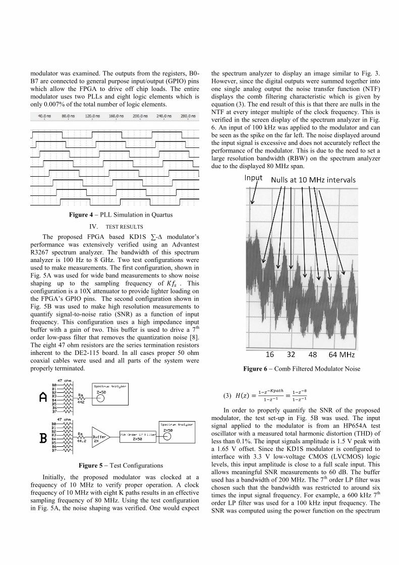
Initially, the proposed modulator was clocked at a
frequency of 10 MHz to verify proper operation. A clock
frequency of 10 MHz with eight K paths results in an effective
sampling frequency of 80 MHz. Using the test configuration
in Fig. 5A, the noise shaping was verified. One would expect
the spectrum analyzer to display an image similar to Fig. 3.
However, since the digital outputs were summed together into
one single analog output the noise transfer function (NTF)
displays the comb filtering characteristic which is given by
equation (3). The end result of this is that there are nulls in the
NTF at every integer multiple of the clock frequency. This is
verified in the screen display of the spectrum analyzer in Fig.
6. An input of 100 kHz was applied to the modulator and can
be seen as the spike on the far left. The noise displayed around
the input signal is excessive and does not accurately reflect the
performance of the modulator. This is due to the need to set a
large resolution bandwidth (RBW) on the spectrum analyzer
due to the displayed 80 MHz span.
Figure 6 Comb Filtered Modulator Noise
(3) 𝐻(𝑧) =1−𝑧−𝐾𝑝𝑎𝑡ℎ
1−𝑧−1 =1−𝑧−8
1−𝑧−1
In order to properly quantify the SNR of the proposed
modulator, the test set-up in Fig. 5B was used. The input
signal applied to the modulator is from an HP654A test
oscillator with a measured total harmonic distortion (THD) of
less than 0.1%. The input signals amplitude is 1.5 V peak with
a 1.65 V offset. Since the KD1S modulator is configured to
interface with 3.3 V low-voltage CMOS (LVCMOS) logic
levels, this input amplitude is close to a full scale input. This
allows meaningful SNR measurements to 60 dB. The buffer
used has a bandwidth of 200 MHz. The 7th
order LP filter was
chosen such that the bandwidth was restricted to around six
times the input signal frequency. For example, a 600 kHz 7th
order LP filter was used for a 100 kHz input frequency. The
SNR was computed using the power function on the spectrum

analyzer. This measurement was repeated for a wide range of
frequencies.
The results of SNR testing are shown in Fig. 7. The
proposed modulator was set up for an 80 MHz effective
sampling rate and the input signal was varied from 10 kHz to
200 kHz. For each input frequency, the SNR was measured
with the 7th
order LP filter in place. The highest SNR achieved
was 55 dB for an input frequency of 10 kHz corresponding to
an effective number of bits (ENOB) of 8.8 bits. As the input
frequency is increased, the SNR falls to a fairly constant range
between 45 dB and 43 dB corresponding to an ENOB of
between 7.3 and 7 bits. After verifying that the proposed
modulator does indeed work, the test was repeated for a higher
effective sampling rate.
Figure 7 Measured SNR with 80 MHz Sampling Rate
An upper limit on the effective sampling rate was chosen
at 450 MHz. This is achieved with a 50 MHz clock frequency.
This limit was chosen due to the fact through-hole mounted
passive components were used. The use of surface mount
components can push this limit higher. The range of input
frequencies was increased to 1 MHz. The results are shown in
Fig. 8. At an input frequency of 10 kHz the SNR increases to
58 dB, a 3 dB improvement over the previous sampling rate
corresponding to an ENOB of 9.3 bits. Within the same
frequency range up to 200 kHz, the SNR stays above 50 dB
which is a significant improvement over the 80 MHz sampling
rate. As the input frequency rises to 1 MHz, the SNR drops
steadily to a minimum of 42dB.
V. CONCLUSION
Through the use of passive RC components and KD1S
principles, a medium resolution, wide-bandwidth ADC was
implemented using a small number of logic elements on an
FPGA. The logic element budget for the proposed ∑-∆
modulator is very low at only 0.007% of the total number of
available logic elements. With modern FPGAs, and small
SMD passive components, effective sampling rates into the
GHz range should be possible. Furthermore, the sophisticated
PLLs available on FPGAs could allow for a wide range of
sampling frequencies and even dynamic adjustment of
sampling rates. For many applications, an ADC built around
the proposed ∑-∆ modulator could prove to be the lowest cost
ADC option for FPGA based systems.
REFERENCES
[1] Baker, R. Jacob, CMOS Mixed-Signal Circuit Design, Second
Edition, John Wiley and Sons, Inc., 2009
[2] Fiel Cordeiro, R.; Oliveira, A.S.R.; Vieira, J.; Silva, N.V.,
"Gigasample Time-Interleaved Delta-Sigma Modulator for
FPGA-Based All-Digital Transmitters," Digital System Design
(DSD), 2014 17th Euromicro Conference on , vol., no.,
pp.222,227, 27-29 Aug. 2014
[3] King, E.; Aram, F.; Fiez, T.; Galton, I., "Parallel Delta-Sigma
A/D Conversion," Custom Integrated Circuits Conference,
1994., Proceedings of the IEEE 1994 , vol., no., pp.503,506, 1-4
May 1994
[4] Saxena, V.; Kaijun Li; Geng Zheng; Jacob Baker, R., "A K-
Delta-1-Sigma Modulator For Wideband Analog to Digital
Conversion," Circuits and Systems, 2009. MWSCAS '09. 52nd
IEEE International Midwest Symposium on , vol., no.,
pp.411,414, 2-5 Aug. 2009
[5] Saxena, Vishal, “K-Delta-1-Sigma Modulators for Wideband Analog-to-Digital Conversion”, Ph.D. dissertation, ECE, Boise State University, Boise, ID, 2010.
[6] Roy, A.; Baker, R.J., "A Passive 2nd-order Sigma-Delta Modulator for Low-Power Analog-to-Digital Conversion," Circuits and Systems (MWSCAS), 2014 IEEE 57th International Midwest Symposium on , vol., no., pp.595,598, 3-6 Aug. 2014
[7] Cyclone IV Device Handbook, Vol. 1., Altera Corp., San Jose., CA, 2014, pp. 15-21.
[8] Low Pass LC Filter Modules, Coilcraft., Cary., IL, 2013, pp. 1-2.
Figure 8 Measured SNR with 450 MHz Sampling Rate