a new era in power electronics with gallium...
TRANSCRIPT

6
TECHNIK & TRENDST
T1 A New Era in Power Electronics with Gallium Nitride
Abstract
Low- and high-power applications such as USB-PD adap-ters and server power supplies can benefit several ways from eMode GaN HEMTs. Using GaN technology enables quanti-tatively better designs compared to the next best silicon al-ternatives. In this technical article we will discuss the benefits of eMode GaN HEMT power devices corroborated by per-formance analysis results and also provide insight into cor-responding topologies, choice of magnetics and switching frequencies to take the full benefit of the next generation of power devices.
1 Introduction
The commercial availability of wide bandgap power semicon-ductors with their significantly better figures of merit raises some fundamental questions on the agenda of many custom-ers: How much better are system solutions based on these wide bandgap components in terms of density and efficien-cy? To what extent can silicon based solutions follow at the potential expense of more complex topologies and control schemes?
This article tries to give answers to these questions for two major application fields, server power supplies for datacenters and compact chargers.
GaN HEMTs as lateral power devices have an order of magnitude lower gate charge and output charge compared to their silicon counterparts. Combined with virtually zero reverse recovery charge it enables hard commutation of reverse con-ducting devices. Thus, GaN supports simpler topologies and an optimization of control methods seamlessly changing be-tween soft switching and (partial) hard switching. Even though hard commutation is acceptable for silicon based power de-vices in low and medium voltage classes, Superjunction de-vices as prominent technology in the 600 V class prevent any such operation due to losses and voltage overshoots. The de-signer of AC/DC applications has three choices as next best alternatives to the use of wide bandgap devices: single ended topologies such as boost converter as a power factor correc-tion stage, strict avoidance of hard commutation through cor-responding control methods such as triangular current mode (TCM) operation in totem-pole PFC, or the use of cascaded converter architecture where the voltage stress is distributed to several series connected converter stages.
While single ended topologies may not comply with efficien-cy targets, alternative solutions such as the dual boost may not comply with space or cost targets. Even though cascaded solu-tions have demonstrated their ability to reach both efficiency and density targets [1], control efforts remain challenging and may limit the use of this concept to the high power segment only.
The design options for highly efficient and compact ser-ver power supplies are narrowing down to silicon based TCM
operation of interleaved totem-pole legs versus a CCM/TCM GaN based totem-pole stage followed by a DC/DC converter, typically being based on an LLC converter.
Vice versa, the design options for compact chargers are significantly narrowing down when trying to overcome density targets of 20 W/in³ for a 65 W adapter. The need to recuper-ate the energy in the leakage inductance and to provide zero voltage switching in most or all operation conditions rules out much of the single ended topology choices.
In both examples being as diverse as a 65 W adapter or a 3 kW power supply this paper explores the value of GaN HEMTs in comparison to next best silicon alternatives.
2 Device concepts
As the race is set between GaN HEMTs versus their silicon counterpart, Superjunction devices being evidently the best alternative, let’s start with a brief review of the latest technol-ogy achievements.
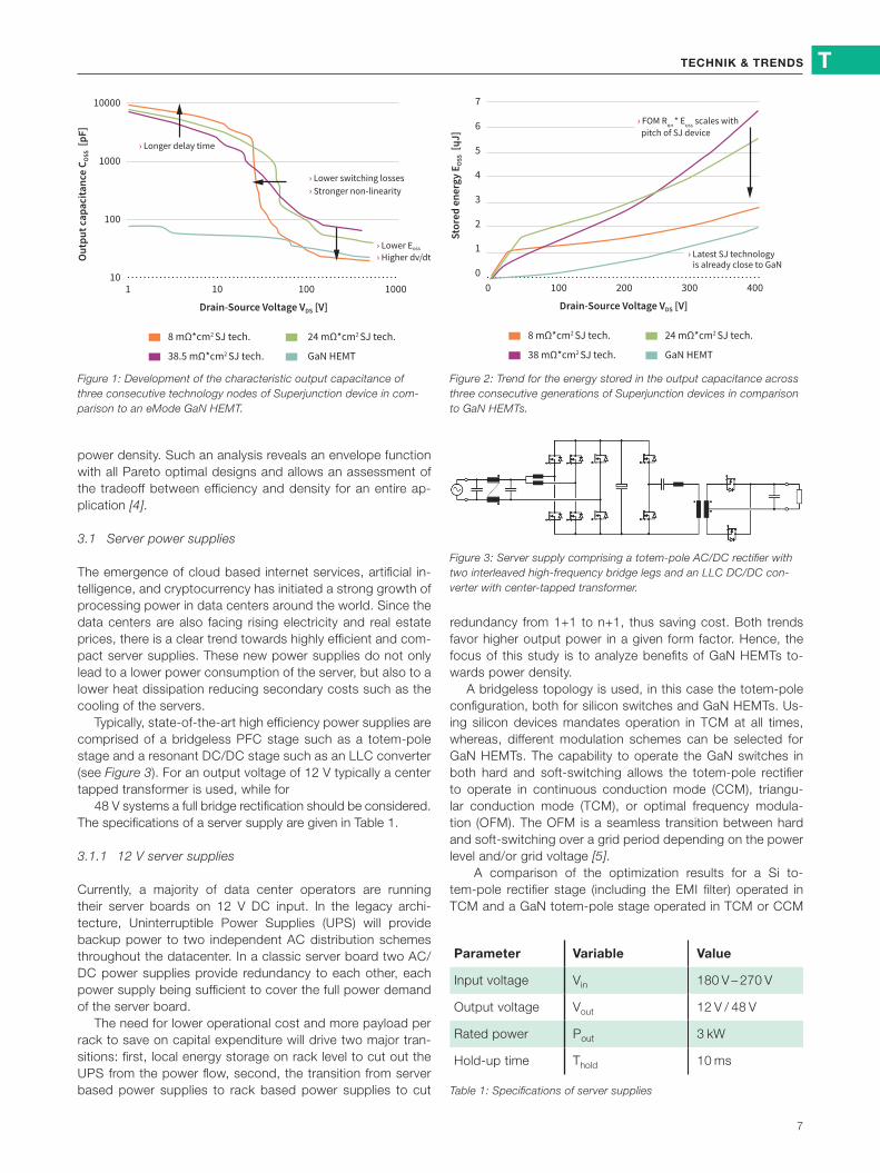
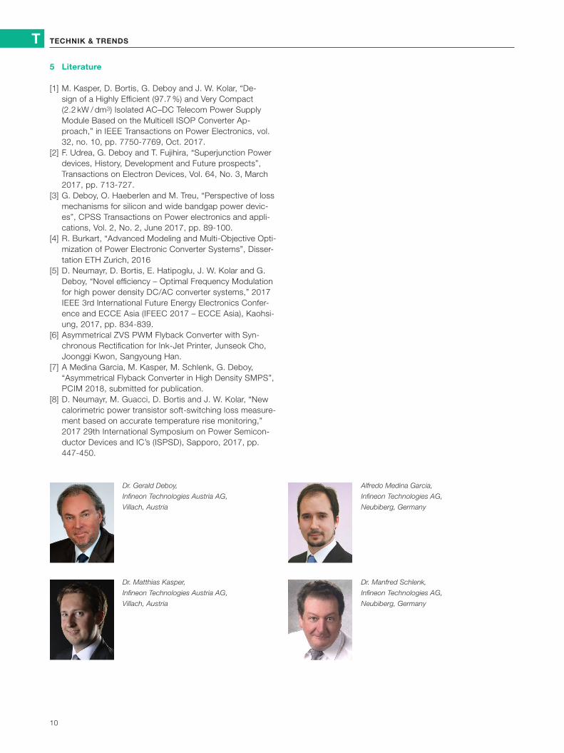
Superjunction devices have pushed for more than a de-cade towards ever lower on-state resistance [2], which in turn reduces the device capacitances and makes the devices in-herently faster switching. Figure 1 shows the output capaci-tance characteristics of three subsequent generations of Su-perjunction transistors versus an eMode GaN HEMT. Figure 2 shows the energy stored in the output capacitance.
Even though the output capacitance of GaN is significantly lower in the low voltage range, the energy stored in the output capacitance is comparatively close to the values achieved by Superjunction devices. Since this energy is dissipated as heat in every switching cycle during hard switching transients, it is already obvious from this graph that the true value of GaN will be in half bridge based circuits and will be limited in single ended topologies.
Whereas in single ended topologies the Eoss parameter is governing loss mechanisms, in half bridge based circuits the charge stored in the output capacitance [3] and the reverse recovery charge is commanding the losses. While Superjunc-tion devices are optimized for an extremely low Eoss figure of merit, GaN HEMTs offer a much more favorable Qoss figure of merit, with the first generation already being one order of mag-nitude better than their silicon counterparts.
3 Application examples
To evaluate, quantitatively, the performance improvements of-fered by wide bandgap power devices, multi-objective opti-mizations were performed for each application. This method allows us to consider all available degrees of freedom in the converter design such as various topologies, interleaving of stages, switching frequencies, and semiconductor usage, and yields as a result for each potential design efficiency and
7
TECHNIK & TRENDS T
power density. Such an analysis reveals an envelope function with all Pareto optimal designs and allows an assessment of the tradeoff between efficiency and density for an entire ap-plication [4].
3.1 Server power supplies
The emergence of cloud based internet services, artificial in-telligence, and cryptocurrency has initiated a strong growth of processing power in data centers around the world. Since the data centers are also facing rising electricity and real estate prices, there is a clear trend towards highly efficient and com-pact server supplies. These new power supplies do not only lead to a lower power consumption of the server, but also to a lower heat dissipation reducing secondary costs such as the cooling of the servers.
Typically, state-of-the-art high efficiency power supplies are comprised of a bridgeless PFC stage such as a totem-pole stage and a resonant DC/DC stage such as an LLC converter (see Figure 3). For an output voltage of 12 V typically a center tapped transformer is used, while for
48 V systems a full bridge rectification should be con sidered. The specifications of a server supply are given in Table 1.
3.1.1 12 V server supplies
Currently, a majority of data center operators are running their server boards on 12 V DC input. In the legacy archi-tecture, Uninterruptible Power Supplies (UPS) will provide backup power to two independent AC distribution schemes throughout the datacenter. In a classic server board two AC/DC power supplies provide redundancy to each other, each power supply being sufficient to cover the full power demand of the server board.
The need for lower operational cost and more payload per rack to save on capital expenditure will drive two major tran-sitions: first, local energy storage on rack level to cut out the UPS from the power flow, second, the transition from server based power supplies to rack based power supplies to cut
redundancy from 1+1 to n+1, thus saving cost. Both trends favor higher output power in a given form factor. Hence, the focus of this study is to analyze benefits of GaN HEMTs to-wards power density.
A bridgeless topology is used, in this case the totem-pole configuration, both for silicon switches and GaN HEMTs. Us-ing silicon devices mandates operation in TCM at all times, whereas, different modulation schemes can be selected for GaN HEMTs. The capability to operate the GaN switches in both hard and soft-switching allows the totem-pole rectifier to operate in continuous conduction mode (CCM), triangu-lar conduction mode (TCM), or optimal frequency modula-tion (OFM). The OFM is a seamless transition between hard and soft-switching over a grid period depending on the power level and/or grid voltage [5].
A comparison of the optimization results for a Si to-tem-pole rectifier stage (including the EMI filter) operated in TCM and a GaN totem-pole stage operated in TCM or CCM
Figure 3: Server supply comprising a totem-pole AC/DC rectifier with two interleaved high-frequency bridge legs and an LLC DC/DC con-verter with center-tapped transformer.
7
6
5
4
3
2
1
0
Drain-Source Voltage VDS [V]
Sto
red
en
erg
y E
OS
S [
ɥJ
]
8 mΩ*cm2 SJ tech. 24 mΩ*cm2 SJ tech.
38 mΩ*cm2 SJ tech. GaN HEMT
› FOM Ron
* Eoss
scales with
pitch of SJ device
› Latest SJ technology is already close to GaN
0 100 200 300 400
Figure 2: Trend for the energy stored in the output capacitance across three consecutive generations of Superjunction devices in comparison to GaN HEMTs.
10000
1000
100
10
Drain-Source Voltage VDS [V]
Ou
tpu
t ca
pa
cita
nce
CO
SS [
pF
]
8 mΩ*cm2 SJ tech. 24 mΩ*cm2 SJ tech.
38.5 mΩ*cm2 SJ tech. GaN HEMT
› Longer delay time
› Lower switching losses
› Lower Eoss
› Higher dv/dt
› Stronger non-linearity
1 10 100 1000
Figure 1: Development of the characteristic output capacitance of three consecutive technology nodes of Superjunction device in com-parison to an eMode GaN HEMT.
Parameter Variable Value
Input voltage Vin 180 V – 270 V
Output voltage Vout 12 V / 48 V
Rated power Pout 3 kW
Hold-up time Thold 10 ms
Table 1: Specifications of server supplies

8
TECHNIK & TRENDST
is shown in Figure 4. Both systems are optimized for 50 per-cent of the rated power and evaluated at nominal operating voltages. In the results, the volume of the power electronics including the PCB and additional air between the components is considered, excluding the case. The results clearly indicate the improved performance of the GaN designs, especially in the area of high power density. An analysis of the designs using GaN transistors reveals that the TCM modulation offers a benefit compared to CCM specifically in the region of high-est power density.
In a similar manner, the LLC stage has been optimized for Si and GaN semiconductors. The results are shown in Figure 5. As can be seen, GaN provides a simultaneous improve-ment of efficiency and power density.
Finally, the optimization results of the entire systems are shown in Figure 6. The results include all power electronic components, auxiliary electronics, PCB and 20 percent of additional volume which was added to account for non-ideal placement of the components. The connectors and the cas-ing with standoff are not included.
The result clearly indicates a path towards 3 kW in a giv-en form factor such as the 68 mm × 41 mm × 184 mm flex slot size, thus nearly doubling the output power in this box size. Comparing to off the shelf solutions delivering 1600 W in this
form factor, we not only nearly double the power but increase efficiency in average by 4 percent without increasing dissipa-ted heat within the power supply (see Figure 7).
3.2 Universal mobile device charger
The growing popularity of mobile electronics devices such as laptop, mobile phones, tablets, e-book readers and smart watches has led to a wide range of different charger types. In order to reduce electronic waste and to simplify the user ex-perience, the need for a universal adapter with high efficiency and high power density has become evident. For this purpose the USB-PD standard has been introduced which supports a wide range of output voltages (5 V to 20 V) with power levels up to 65 W.
To identify the most suitable topology for a high density USB-PD adapter, several topology options have been eval-uated by means of multi-objective optimizations. The con-sidered topologies include: PFC flyback with secondary side power pulsation buffer, flyback converter with a fixed (high) output voltage and subsequent buck converter, flyback con-verter with wide output voltage range, cascaded asymmet-rical PWM flyback where the primary side consists of two cas caded half-bridges, and asymmetrical PWM flyback. The
Power density [W/inch3]
E�ic
ienc
y [%
]
50 100 150 200 250
100
99.8
99.6
99.4
99.2
99.0
98.8
98.6
98.4
98.2
98.0
GaN Si
Figure 4: Optimization results for the totem-pole PFC stage, including the EMI filter, with GaN or Si.
E�ic
ienc
y [%
]
0 20 40 60 80 100 120 140
98.0
97.5
97.0
96.5
96.0
95.5
95
Power density [W/inch3]
GaN Si
Figure 6: Optimization results of the entire 12 V server supply for ei-ther GaN or Si semiconductors.
Pout [W]
E�ic
ienc
y [%
]
0 500 1000 1500 2000 2500 3000
100
98
96
94
92
90
88
86
84
82
80
Optimized power supply Typ. Platinum power supply
Figure 7: Evaluation of the 12 V GaN server supply with a power densi-ty of 100 W / in3 in dependence of the output power.
Power density [W/inch3]
E�ic
ienc
y [%
]
0 50 100 150 200 250 300
100
99.5
99.0
98.5
98.0
97.5
97.0
96.5
96.0
95.5
95.0
GaN Si
Figure 5: Optimization results for the LLC stage with GaN or Si.

9
TECHNIK & TRENDS T
optimization results are shown in Figure 8 for full load opera-tion at worst case input voltage (Vin = 90 V) and highest output current ( Iout = 4 A). In addition, the thermal limit line is shown, which defines the minimum efficiency required for a given power density in order to keep the surface temperature of the adaptor below 70 °C. Only designs above this line possess the necessary efficiency required to dissipate the generated heat passively (i.e. natural convection and radiation) without exceeding the thermal limit of the case. This clearly shows that the target of highest power density is inevitably linked to highest conversion efficiency, underlining the necessity of a comprehensive multi-objective optimization approach.
The optimization results reveal the asymmetrical flyback (see Figure 8) is the best suited topology among the consid-ered candidates for highly compact chargers since it offers the highest efficiency. This topology features ZVS of the pri-mary side half-bridge by utilizing the magnetization current, and ZCS of the synchronous rectification switch, laying the foundation for highest conversion efficiency. The converter is operated with a fixed ON-time of the low-side switch of the
primary half-bridge, which is determined by the resonance fre-quency, and a varying ON-time of the high-side switch, which depends on the output voltage [6]. This results in a varying switching frequency.
Based on the optimization results, a 65 W prototype em-ploying 500 V / 140 mΩ MOSFETs has been developed (see Figure 9) [7]. It supports USB-PD with different output volt-age profiles ranging from 5 V / 3 A to 20 V / 3.25 A. The oper-ation frequency varies from 100 kHz to 220 kHz depending on the input and output voltages. The prototype achieves a maximum efficiency of 94.8 percent, while the lowest full-load efficiency at Vin = 90 V is 93 percent as shown in Figure 11.
To push the power density to even higher levels, the use of GaN HEMTs becomes mandatory, as they allow the efficien-cy of the converter to be increased and thus to move away from the thermal limit. The first advantage of GaN is given by the greatly reduced Qoss charge, which enables ZVS with lower magnetizing current. Thus, the conduction losses in the switches as well as the transformer can be reduced. Further-more, due to the lower gate charge the gate driving losses are reduced. Last but not least, the losses associated with the charging/discharging of Coss capacitance of the switches during ZVS are also lower in GaN HEMTs than in Superjunc-tion MOSFETs [8]. As a result, the efficiency of the entire sys-tem can be increased by around 0.4 percent at full load over the entire input voltage range, as depicted in Figure 11.
4 Summary
The application studies performed show a clear value for eMode GaN HEMTs in a wide range of applications span-ning low power adapters to high power server designs. GaN HEMTs allow us to push both efficiency and density frontiers.
This paper demonstrated a path towards 98.5 percent ef-ficiency in 48V servers and towards a density of 100 W/in³ for 12 V servers thus offering large benefits in terms of OPEX and CAPEX savings.
For mobile applications GaN offers hitherto unachievable small form factors beyond 20 W/in³ for 65 W USB-PD adapters.
Figure 8: Multi-objective optimization results of several different ad-aptor concepts for full load (Pout = 65 W), Vout = 20 V and low line (Vin = 90 V) operation.
Figure 9: Asymmetrical PWM flyback with synchronous rectification.
Figure 10: Prototype of the 65 W USB-PD adapter based on the asym-metrical PWM flyback topology. The prototype features a power densi-ty of 27 W / in3 (cased: 20 W / in3).
VAC [V]
E�ic
ienc
y [%
]
90 110 130 150 180 210 230 250
95.5
95.0
94.5
94.0
93.5
93.0
92.5
E�iciency GaN E�iciency Si
Figure 11: Red curve: Measured full load efficiency (Pout = 65 W) of the prototype in dependency of the input voltage for an output volt-age of Vout = 20 V. Blue curve: Efficiency improvement possibility with 600 V / 190 mΩ GaN HEMTs instead of 500 V / 140 mΩ Si MOSFETs.
10
TECHNIK & TRENDST
5 Literature
[1] M. Kasper, D. Bortis, G. Deboy and J. W. Kolar, “De-sign of a Highly Efficient (97.7 %) and Very Compact (2.2 kW / dm3) Isolated AC–DC Telecom Power Supply Module Based on the Multicell ISOP Converter Ap-proach,” in IEEE Transactions on Power Electronics, vol. 32, no. 10, pp. 7750-7769, Oct. 2017.
[2] F. Udrea, G. Deboy and T. Fujihira, “Superjunction Power devices, History, Development and Future prospects”, Transactions on Electron Devices, Vol. 64, No. 3, March 2017, pp. 713-727.
[3] G. Deboy, O. Haeberlen and M. Treu, “Perspective of loss mechanisms for silicon and wide bandgap power devic-es”, CPSS Transactions on Power electronics and appli-cations, Vol. 2, No. 2, June 2017, pp. 89-100.
[4] R. Burkart, “Advanced Modeling and Multi-Objective Opti-mization of Power Electronic Converter Systems”, Disser-tation ETH Zurich, 2016
[5] D. Neumayr, D. Bortis, E. Hatipoglu, J. W. Kolar and G. Deboy, “Novel efficiency – Optimal Frequency Modulation for high power density DC/AC converter systems,” 2017 IEEE 3rd International Future Energy Electronics Confer-ence and ECCE Asia (IFEEC 2017 – ECCE Asia), Kaohsi-ung, 2017, pp. 834-839.
[6] Asymmetrical ZVS PWM Flyback Converter with Syn-chronous Rectification for Ink-Jet Printer, Junseok Cho, Joonggi Kwon, Sangyoung Han.
[7] A Medina Garcia, M. Kasper, M. Schlenk, G. Deboy, “Asymmetrical Flyback Converter in High Density SMPS”, PCIM 2018, submitted for publication.
[8] D. Neumayr, M. Guacci, D. Bortis and J. W. Kolar, “New calorimetric power transistor soft-switching loss measure-ment based on accurate temperature rise monitoring,” 2017 29th International Symposium on Power Semicon-ductor Devices and IC’s (ISPSD), Sapporo, 2017, pp. 447-450.
Dr. Gerald Deboy,
Infineon Technologies Austria AG,
Villach, Austria
Alfredo Medina Garcia,
Infineon Technologies AG,
Neubiberg, Germany
Dr. Matthias Kasper,
Infineon Technologies Austria AG,
Villach, Austria
Dr. Manfred Schlenk,
Infineon Technologies AG,
Neubiberg, Germany