a novel 2.4-ghz low-profile mimo antenna with
TRANSCRIPT

ADVANCED ELECTROMAGNETICS, VOL. 9, NO. 2, OCTOBER 2020
A Novel 2.4-GHz Low-Profile MIMO Antenna with Reconfigurable Frequency-Selective Reflectors
Ching-Han Tsai*, Jai-Shan Sun, Shyh-Jong Chung, and Jenn-Hwan Tarng
Institute of Communications Engineering, National Chiao Tung University, Hsinchu, Taiwan
*corresponding author, E-mail: [email protected]
Abstract In this paper, a novel low-profile multiple-input multiple-output (MIMO) antenna system is presented for WiFi IEEE 802.11a/b/g/n/ac/ax applications. The proposed compact 2.4-GHz antenna system employs two beam-switching antenna cells for MIMO operation. Each antenna cell is composed of four reconfigurable frequency-selective reflectors (RFSRs) and a one-to-four switching feeding network. The RFSRs are constructed using a one-wavelength metal loop resonator, which, by controlling the switching network, functions as a radiating antenna or a wave reflector to reflect beams to a specific direction. The feeding switching network utilizes PIN diodes to adjust the phase and impedance required for changing the operational status of each RFSR. The overall dimensions of the antenna system, including the metallic ground, are 120 mm ´ 120 mm ´ 9.5 mm. Moreover, the measured operational bandwidth of the 2.4-GHz antenna is approximately 100 MHz, and the radiation efficiency of each directed beam is 40%–70%.
1. Introduction Multiple-input multiple-output (MIMO) technology plays an important role in wireless communication systems. Because MIMO technology increases the data rate, reduces multipath fading, and suppresses co-channel interference [1], this technique is widely used in consumer and portable electronic products, such as WiFi access points (APs), cellphones, and notebook computers [2–5]. To realize these favorable characteristics, multiple antennas with pattern diversity are required in MIMO systems. From the viewpoint of commercialization, a compact antenna is critical in modern MIMO designs. Achieving this is a challenge because high mutual coupling may occur when many antenna units are placed proximally in a small housing, which reduces the overall system performance.
In the last decade, several MIMO antennas with reconfigurable radiation patterns have been proposed. In [6–15], a unidirectional antenna design based on the Yagi–Uda antenna concept was proposed using various combinations of directors and reflectors to achieve pattern-reconfigurable features. In this approach, parasitic elements can be designed to be shorter or longer than active elements for ensuring that the pattern is pulled toward the desired direction. To build pattern-reconfiguration features, switches are introduced for
controlling the properties of the parasitic elements. Another approach for constructing pattern-
reconfigurable antennas involves utilizing switched arrays [16–20]. A phased array can redirect the main beam by appropriately adjusting the feeding phases of the active elements. In [16], adequate antenna phases were established by shifting the feeding point of the power divider. The direction of the main beam varied with the operating frequencies of the antenna because the phase differences between paths changed with the operating frequency. And, in [19], the distribution of phase angles at each port in the feeding network was altered by moving a metal-coated slab. In our previous studies [21,22], we developed a radiation pattern diversity antenna, which is different from the aforementioned two types of reconfigurable antennas, by combining the concepts of reconfigurable frequency-selective reflectors (RFSRs) and right-angle corner reflector antennas.
Although the pattern-reconfiguration function was successfully achieved by utilizing the antennas fabricated in the aforementioned studies, the overall antenna sizes were large and did not fulfill the requirements of cutting-edge MIMO antennas, such as compact size, light weight, and low profile. A few printed dipole-like reconfigurable antennas with electrically small sizes have been reported [23,24]. However, due to their dipole characteristics, integrating such balanced antennas into printed circuit boards (PCBs) and other circuitry is difficult because the radiated current is drastically affected by the large ground plane of the PCB; moreover, a coaxial cable is unsuitable for being used as the feed line because of its unbalanced structure. Thus, the aforementioned antennas would not be suitable for use in portable devices, such as smartphones and WiFi APs.
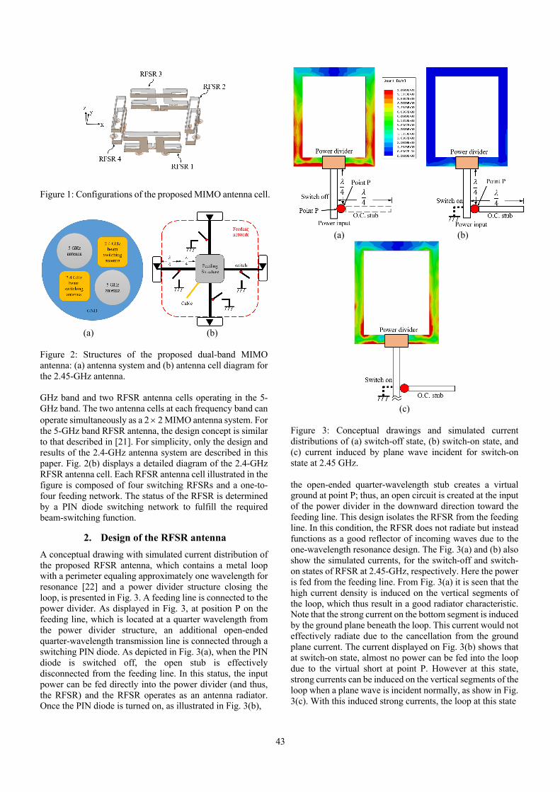
For improving antenna integration with PCB circuitry to increase productivity and minimize antenna size, we propose a novel low-profile beam-reconfigurable antenna used for ceiling-mounted WIFI-AP application, as illustrated in Fig. 1. The proposed antenna cell comprises four low-profile RFSRs, where the spacing between RFSRs 1 and 3 is a quarter wavelength, which is the same as that between RFSRs 2 and 4. To achieve the beam-reconfiguration feature, the four RFSRs are designed to be configured as radiators or reflectors. With this antenna cell design, a dual-band MIMO antenna system is constructed, as depicted in Fig. 2(a). The system contains two RFSR antenna cells operating in the 2.4-
43
Figure 1: Configurations of the proposed MIMO antenna cell.
(a) (b)
Figure 2: Structures of the proposed dual-band MIMO antenna: (a) antenna system and (b) antenna cell diagram for the 2.45-GHz antenna. GHz band and two RFSR antenna cells operating in the 5-GHz band. The two antenna cells at each frequency band can operate simultaneously as a 2 2 MIMO antenna system. For the 5-GHz band RFSR antenna, the design concept is similar to that described in [21]. For simplicity, only the design and results of the 2.4-GHz antenna system are described in this paper. Fig. 2(b) displays a detailed diagram of the 2.4-GHz RFSR antenna cell. Each RFSR antenna cell illustrated in the figure is composed of four switching RFSRs and a one-to-four feeding network. The status of the RFSR is determined by a PIN diode switching network to fulfill the required beam-switching function.
2. Design of the RFSR antenna A conceptual drawing with simulated current distribution of the proposed RFSR antenna, which contains a metal loop with a perimeter equaling approximately one wavelength for resonance [22] and a power divider structure closing the loop, is presented in Fig. 3. A feeding line is connected to the power divider. As displayed in Fig. 3, at position P on the feeding line, which is located at a quarter wavelength from the power divider structure, an additional open-ended quarter-wavelength transmission line is connected through a switching PIN diode. As depicted in Fig. 3(a), when the PIN diode is switched off, the open stub is effectively disconnected from the feeding line. In this status, the input power can be fed directly into the power divider (and thus, the RFSR) and the RFSR operates as an antenna radiator. Once the PIN diode is turned on, as illustrated in Fig. 3(b),
(a) (b)
(c)
Figure 3: Conceptual drawings and simulated current distributions of (a) switch-off state, (b) switch-on state, and (c) current induced by plane wave incident for switch-on state at 2.45 GHz. the open-ended quarter-wavelength stub creates a virtual ground at point P; thus, an open circuit is created at the input of the power divider in the downward direction toward the feeding line. This design isolates the RFSR from the feeding line. In this condition, the RFSR does not radiate but instead functions as a good reflector of incoming waves due to the one-wavelength resonance design. The Fig. 3(a) and (b) also show the simulated currents, for the switch-off and switch-on states of RFSR at 2.45-GHz, respectively. Here the power is fed from the feeding line. From Fig. 3(a) it is seen that the high current density is induced on the vertical segments of the loop, which thus result in a good radiator characteristic. Note that the strong current on the bottom segment is induced by the ground plane beneath the loop. This current would not effectively radiate due to the cancellation from the ground plane current. The current displayed on Fig. 3(b) shows that at switch-on state, almost no power can be fed into the loop due to the virtual short at point P. However at this state, strong currents can be induced on the vertical segments of the loop when a plane wave is incident normally, as show in Fig. 3(c). With this induced strong currents, the loop at this state

44
(a) (b)
(c) (d)
Figure 4: Steps toward the final design target of the proposed RFSR: (a) Step 1, (b) Step 2, (c) Step 3, and (d) Step 4. would thus behave as a good reflector (see section 2.2). The simulated result shows that by controlling the states of PIN diode, the RFSR can be switched between reflector and radiator easily.
2.1. Antenna mode
To make the antenna design compact, the RFSR loop was bent in the order displayed in Figs. 4(a)–(d). The design procedure started from bringing down the height of the one-wavelength loop (Fig. 4(a)) to a low-profile resonant loop (Fig. 4(b)). Here the height of RFSR was chosen for meeting the target in ceiling-mounted application. Since the distance between RFSRs should be a quarter-wavelength, the reduced-height loop was then folded by selecting a RFSR bottom length close to a quarter-wavelength, as depicted in Figs. 4(c)-(d). This geometry can effectively reduce the loop height and sustain the reflection cross section to ensure that the loop performs as a reflector. The finished RFSR geometry is illustrated in Fig. 5(a)-(c) with final designed dimensions. The RFSR loop was made of a copper–nickel–zinc alloy called C7521, which is commonly used in industrial applications because it is inexpensive and easy to produce. The RFSR was mounted at the center of a circular FR4 substrate whose top side was coppered as the ground, as illustrated in Fig. 5(a). The diameter of the substrate plane was 120 mm, which is very small considering the wavelength corresponding to 2.4-GHz. Two supporting guide pins originating from the RFSR were soldered to the backside pad to enhance the producibility of the structure. A 70-Ω feeding line was designed for the FR4 substrate. For analyzing the proposed structure, we employed the full-wave electromagnetic simulator ANSYS HFSS (ANSYS, Inc., PA, USA). Fig. 5(c) illustrates the detailed geometry of the power divider structure; the dimensions of this structure were fine-tuned to optimize the performance of the RFSR. Fig. 6(a) illustrates the simulated return loss (RL) of the RFSR antenna. The 10-dB RL bandwidth was 170 MHz, with a maximum
(a)
(b)
(c)
Figure 5: Geometry of the proposed miniaturized RFSR: (a) side view of the RFSR, (b) eagle view of the RFSR, and (c) geometry of the power divider structure. H = 9.5 mm, Hp = 2 mm, Hh = 0.5 mm, T = 0.3 mm, Wr = 4.6 mm, G = 4 mm, Gr = 1 mm, Lr = 27.6 mm, Lr1 = 7.5 mm, Lr2 = 4 mm, Lr3 = 11.8 mm, Lp = 9 mm, Lp1 = 2.25 mm, Lp2 = 1.5 mm, Lp3 = 0.38 mm, Wp = 3 mm, and Wp1 = 0.8 mm.
RL of 13 dB at 2.45-GHz. The simulated horizontal-plane (H-cut) and vertical-plane (E-cut) radiation patterns are illustrated in Figs. 6(b) and (c), respectively. The simulation patterns were rather similar to those of a monopole antenna on a finite ground plane. The calculated peak gain of the RFSR antenna was 2.6 dBi around the angle of 𝜃 = 45°. Because the size of the ground plane was smaller than one wavelength, some power leaked to the backside of the ground. The front-to-back peak power ratio was close to 4 dB.
2.2. Reflector mode
When the PIN diode is switched on, the RFSR is isolated from the feeding circuitry and behaves as a wave reflector. To analyze the reflection effect of the isolated RFSR when a plane wave is normally incident on the structure, we developed the simulation model illustrated in Fig. 7(a). In this model, the RFSR is placed inside a rectangular tube with

45
(a)
(b) (c)
Figure 6: (a) S-parameters of the proposed RFSR, (b) horizontal-cut antenna pattern, and (c) vertical-cut antenna pattern. perfect electric conductors at the top and bottom and perfect magnetic conductors on the sides. Two wave ports attached to the ends of the tube are used to extract the reflection and transmission coefficients of the isolated RFSR. The dominant propagating mode with vertical polarization of the wave-guiding tube is used to simulate the incident wave from port 1. The calculated scattering parameters and current distribution of the RFSR are illustrated in Figs. 7(b) and (c), respectively. Fig. 7(b) indicates that in the frequency range of 2.4–2.5 GHz, the reflection coefficient (S11) is higher than −0.8 dB and the transmission coefficient (S21) is lower than −10 dB. Moreover, the phase of the reflection coefficient at the feed position of the RFSR [plane F in Fig. 7 (a)] is approximately 180° around the center frequency. These findings imply that the isolated RFSR can efficiently reflect incident waves and function well as a metal plate reflector. To acquire a more thorough understanding, consider the current induced on the RFSR at 2.45-GHz, as illustrated in Fig. 7(c). Due to vertical polarization of the incident wave and the resonance property of the structure, the induced current is mainly distributed in the vertical segments of the RFSR. This induced vertical current radiates vertical electric fields toward the two ends of the guiding tube. These fields cancel the incident wave at port 2 and simultaneously produce a reflected wave at port 1. Due to the opposite current directions, the radiation fields associated with the currents induced in various horizontal segments of the RFSR cancel each other, which results in the production of a negligible amount of spurious radiation.
(a)
(b)
(c)
Figure 7: (a) RFSR in a rectangular tube in reflector mode simulation. a = 31 mm, b = 16 mm, c = 120 mm. (b) S-parameters of the proposed RFSR. (c) Induced current for RFSR operating in the reflector mode at 2.45 GHz.
3. Integration of MIMO antenna system
3.1. Beam-switching circuit design
As illustrated in Fig. 2(b), the proposed MIMO antenna system consists of four RFSR antennas and a beam-switching feeding circuitry. Fig. 8(a) illustrates the design of the one-to-four beam-switching circuit. It consists of a one-to-four power divider located at the center, with each of its output ports connected to a PIN diode switch that can control the RFSR characteristics. The equivalent circuit of the switch section is depicted in Fig. 8(b). As displayed in this figure, the switching section consists of a PIN diode (BAR64-02V, Infineon AG, Germany) with a biasing circuit and a connected quarter-wavelength open stub. This section is used to switch the RFSR between the antenna mode and the reflector mode. For operating the RFSR in the reflector mode, the bias should turn on the PIN diode, which should result in a virtual ground at point P due to the impedance transformation effect of the connected quarter-wavelength open stub. However, the switch-on PIN diode is actually not
Frequency (GHz)2.3 2.4 2.5 2.6
Retu
rn L
oss (
dB)
0
5
10
15
20
Phi =
0
30
6090
120
150
180
210
240270
300
330
-15
-10
-5
0
5
Y
2.45 GHz
X
Theta = 030
60
90
120
150180
210
240
270
300
330
-25-20-15-10-505
Phi = 0o
Phi = 90o
Z
2.45 GHz
Frequency (GHz)2.3 2.4 2.5 2.6
Scat
terin
g co
effic
ient
(dB)
-40
-30
-20
-10
0
Phas
e (de
g)
-240
-210
-180
-150
-120
S11S21Phase of S11 at plan F
46
(a)
(b)
Figure 8: (a) Structure of the RFSR feeding network and (b) circuit diagram of the PIN diode switch.
(a)
(b) (c)
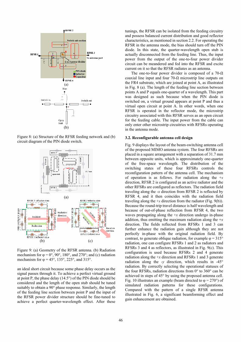
Figure 9: (a) Geometry of the RFSR antenna. (b) Radiation mechanism for φ = 0°, 90°, 180°, and 270°; and (c) radiation mechanism for φ = 45°, 135°, 225°, and 315°. an ideal short circuit because some phase delay occurs as the signal passes through it. To achieve a perfect virtual ground at point P, the phase delay (14.5°) of the PIN diode should be considered and the length of the open stub should be tuned suitably to obtain a 90° phase response. Similarly, the length of the feeding line section between point P and the input of the RFSR power divider structure should be fine-tuned to achieve a perfect quarter-wavelength effect. After these
tunings, the RFSR can be isolated from the feeding circuitry and possess balanced current distribution and good reflector characteristics, as mentioned in section 2.2. For operating the RFSR in the antenna mode, the bias should turn off the PIN diode. In this state, the quarter-wavelength open stub is actually disconnected from the feeding line. Thus, the input power from the output of the one-to-four power divider circuit can be meandered and fed into the RFSR and excite current on it so that the RFSR radiates as an antenna.
The one-to-four power divider is composed of a 70-Ω coaxial line input and four 70-Ω microstrip line outputs on the FR4 substrate, which are joined at point A, as illustrated in Fig. 8 (a). The length of the feeding line section between points A and P equals one-quarter of a wavelength. This part was designed as such because when the PIN diode is switched on, a virtual ground appears at point P and thus a virtual open circuit at point A. In other words, when one RFSR is operated in the reflector mode, the microstrip circuitry associated with this RFSR serves as an open circuit for the feeding cable. The input power from the cable can only enter other microstrip circuitries with RFSRs operating in the antenna mode.
3.2. Reconfigurable antenna cell design
Fig. 9 displays the layout of the beam-switching antenna cell of the proposed MIMO antenna system. The four RFSRs are placed in a square arrangement with a separation of 31.7 mm between opposite units, which is approximately one-quarter of the free-space wavelength. The distribution of the switching states of these four RFSRs controls the reconfiguration pattern of the antenna cell. The mechanism of operation is as follows. For radiation along the +x direction, RFSR 2 is configured as an active radiator and the other RFSRs are configured as reflectors. The radiation field traveling along the -x direction from RFSR 2 is reflected by RFSR 4, and it then coincides with the radiation field traveling along the +x direction from the radiator (Fig. 9(b)). Because the round-trip travel distance is half wavelength and because of out-of-phase reflection from RFSR 4, the two waves propagating along the +x direction undergo in-phase addition, thus emitting the maximum radiation along the +x direction. The fields reflected from RFSRs 1 and 3 can further enhance the radiation gain although they are not perfectly in-phase with the original radiation field. By contrast, to generate oblique radiation, for example φ = 315° radiation, one can configure RFSRs 1 and 2 as radiators and RFSRs 3 and 4 as reflectors, as illustrated in Fig. 9(c). This configuration is used because RFSRs 2 and 4 generate radiation along the +x direction and RFSRs 1 and 3 generate radiation along the -y direction, which results in -45° radiation. By correctly selecting the operational statuses of the four RFSRs, radiation directions from 0° to 360° can be achieved in steps of 45° by using the proposed antenna cell. Fig. 10 illustrates an example (beam directed to φ = 270°) of simulated radiation patterns for these configurations. Compared with the pattern of a single RFSR antenna illustrated in Fig. 6, a significant beamforming effect and gain enhancement are obtained.
47
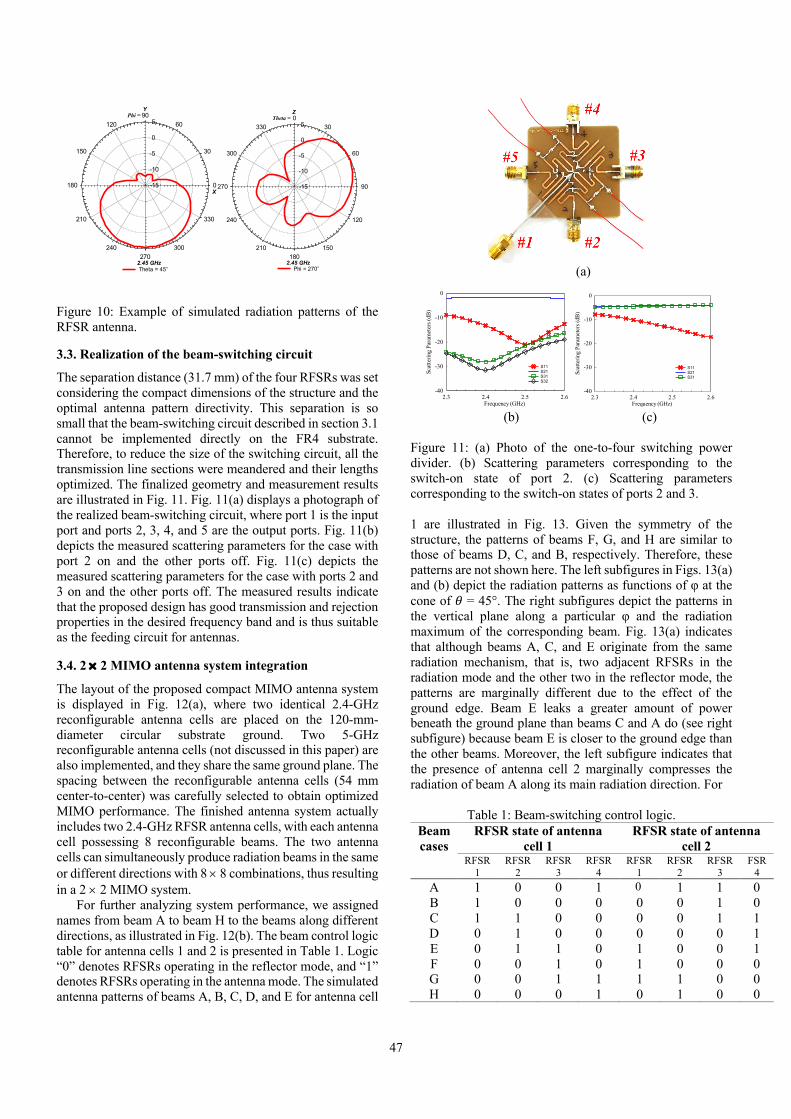
Figure 10: Example of simulated radiation patterns of the RFSR antenna.
3.3. Realization of the beam-switching circuit
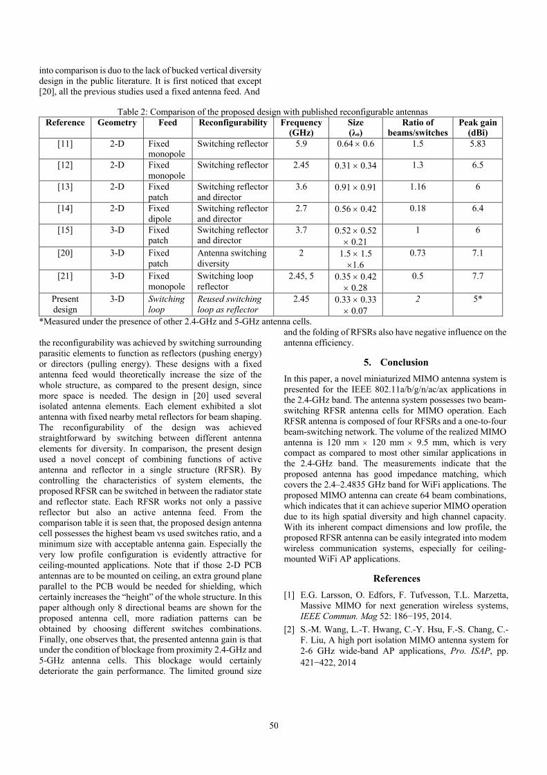
The separation distance (31.7 mm) of the four RFSRs was set considering the compact dimensions of the structure and the optimal antenna pattern directivity. This separation is so small that the beam-switching circuit described in section 3.1 cannot be implemented directly on the FR4 substrate. Therefore, to reduce the size of the switching circuit, all the transmission line sections were meandered and their lengths optimized. The finalized geometry and measurement results are illustrated in Fig. 11. Fig. 11(a) displays a photograph of the realized beam-switching circuit, where port 1 is the input port and ports 2, 3, 4, and 5 are the output ports. Fig. 11(b) depicts the measured scattering parameters for the case with port 2 on and the other ports off. Fig. 11(c) depicts the measured scattering parameters for the case with ports 2 and 3 on and the other ports off. The measured results indicate that the proposed design has good transmission and rejection properties in the desired frequency band and is thus suitable as the feeding circuit for antennas.
3.4. 2 ´ 2 MIMO antenna system integration
The layout of the proposed compact MIMO antenna system is displayed in Fig. 12(a), where two identical 2.4-GHz reconfigurable antenna cells are placed on the 120-mm-diameter circular substrate ground. Two 5-GHz reconfigurable antenna cells (not discussed in this paper) are also implemented, and they share the same ground plane. The spacing between the reconfigurable antenna cells (54 mm center-to-center) was carefully selected to obtain optimized MIMO performance. The finished antenna system actually includes two 2.4-GHz RFSR antenna cells, with each antenna cell possessing 8 reconfigurable beams. The two antenna cells can simultaneously produce radiation beams in the same or different directions with 8 8 combinations, thus resulting in a 2 ´ 2 MIMO system.
For further analyzing system performance, we assigned names from beam A to beam H to the beams along different directions, as illustrated in Fig. 12(b). The beam control logic table for antenna cells 1 and 2 is presented in Table 1. Logic “0” denotes RFSRs operating in the reflector mode, and “1” denotes RFSRs operating in the antenna mode. The simulated antenna patterns of beams A, B, C, D, and E for antenna cell
(a)
(b) (c)
Figure 11: (a) Photo of the one-to-four switching power divider. (b) Scattering parameters corresponding to the switch-on state of port 2. (c) Scattering parameters corresponding to the switch-on states of ports 2 and 3. 1 are illustrated in Fig. 13. Given the symmetry of the structure, the patterns of beams F, G, and H are similar to those of beams D, C, and B, respectively. Therefore, these patterns are not shown here. The left subfigures in Figs. 13(a) and (b) depict the radiation patterns as functions of φ at the cone of 𝜃 = 45°. The right subfigures depict the patterns in the vertical plane along a particular φ and the radiation maximum of the corresponding beam. Fig. 13(a) indicates that although beams A, C, and E originate from the same radiation mechanism, that is, two adjacent RFSRs in the radiation mode and the other two in the reflector mode, the patterns are marginally different due to the effect of the ground edge. Beam E leaks a greater amount of power beneath the ground plane than beams C and A do (see right subfigure) because beam E is closer to the ground edge than the other beams. Moreover, the left subfigure indicates that the presence of antenna cell 2 marginally compresses the radiation of beam A along its main radiation direction. For
Table 1: Beam-switching control logic. Beam cases
RFSR state of antenna cell 1
RFSR state of antenna cell 2
RFSR 1
RFSR 2
RFSR 3
RFSR 4
RFSR 1
RFSR 2
RFSR 3
FSR 4
A 1 0 0 1 0 1 1 0 B 1 0 0 0 0 0 1 0 C 1 1 0 0 0 0 1 1 D 0 1 0 0 0 0 0 1 E 0 1 1 0 1 0 0 1 F 0 0 1 0 1 0 0 0 G 0 0 1 1 1 1 0 0 H 0 0 0 1 0 1 0 0
Phi =
0
30
6090
120
150
180
210
240270
300
330
-15
-10
-5
0
5
Theta = 45o
Y
2.45 GHz
X
Theta = 030
60
90
120
150180
210
240
270
300
330
-15
-10
-5
0
5
Phi = 270o
Z
2.45 GHz
Frequency (GHz)2.3 2.4 2.5 2.6
Scat
terin
g Pa
ram
eter
s (dB
)
-40
-30
-20
-10
0
S11S21S31S32
Frequency (GHz)2.3 2.4 2.5 2.6
Scat
terin
g Pa
ram
eter
s (dB
)
-40
-30
-20
-10
0
S11S21S31

48
(a)
(b)
Figure 12: Proposed MIMO antenna: (a) layout of the proposed MIMO antenna and (b) beam directions of the MIMO antenna. beams B and D, Fig. 13(b) indicates that beam D leaks a greater amount of power beneath the ground plane than beam B because beam D is closer to the ground edge than beam B. Moreover, the maximum radiation of beam B is marginally tilted from the design direction due to the presence of antenna cell 2. Nevertheless, all beam patterns are suitable, with the maximum radiation close to or along the design direction.
4. Experimental result The fabricated MIMO antenna is illustrated in Fig. 14. On the top side of the antenna (Fig. 14 (a)), there exist two 2.4-GHz and two 5-GHz reconfigurable antenna cells. The design concept of the 5-GHz cells is similar to that of the 2.4-GHz cells. However, the four 5-GHz RFSRs have an active antenna placed at their center. These RFSRs no longer operate in the antenna mode but are switched between the reflector mode and the transparency mode. The transparency mode is obtained by destroying the one-wavelength resonance of the RFSR loop by using a PIN diode switch. Fig. 14(b) illustrates the bottom side of the antenna, which houses the control and feeding circuitry. The beam-switching circuit is fed through a mini coaxial cable, and the switching of the PIN diodes is controlled by applying voltages from a
header in the marked red circle in Fig. 14(b). Fig. 15 displays the
(a)
(b)
Figure 13: Simulated radiation patterns of various radiation beams for antenna cell 1: (a) beams A, C, and E and (b) beams B and D. measured RL results for beams A to H of the 2.4-GHz cells. The simulated values are also depicted for comparison. Due to the geometric symmetry of the structure, only the results of antenna cell 1 are presented. The figure indicates that the measured RLs for all beams are higher than 10 dB in the desired operation band of 2.4–2.4835 GHz. Moreover, the measured RLs agree well with the simulated values.
The radiation patterns measured at the horizontal and vertical planes for beams B and D are illustrated in Fig. 16. For beam B, the maximum gain is 3.35 dBi at 2.45-GHz, as measured along φ = 315° and θ = 75°, with an efficiency of 44.28%. The direction along which the maximum gain was measured is shifted by approximately 45° from the design direction (270°). This shift is made because the 5-GHz antenna cell is very close to the radiator RFSR 1 of beam B. Consequently, the blockage effect degrades the gain along the direction φ = 270°. Nevertheless, the front-to-back ratio of beam B is still 8.16 dB, and thus, it can be used in MIMO operation. For beam D, the maximum gain is approximately 2.94 dBi, with an efficiency of 60.11%. Moreover, without blockage from the 5-GHz antenna, the measured radiation patterns agree well with the simulated ones. Fig. 17 illustrates the measured and simulated patterns for beams A, C, and E. For beam A, the maximum gain is 1.79 dBi with an efficiency of 44.31%. The same blockage effect like beam B is observed because the two radiators for beam A are close to the
Phi =
0
30
6090
120
150
180
210
240270
300
330
-15
-10
-5
0
5
Beam A, theta = 45o
Beam C, theta = 45o
Beam E, theta = 45o
Y
2.45 GHz
X
Theta = 030
60
90
120
150180
210
240
270
300
330
-15
-10
-5
0
5
Beam A, phi = 225o
Beam C, phi = 315o
Beam E, phi = 45o
Z
2.45 GHz
Phi =
0
30
6090
120
150
180
210
240270
300
330
-15
-10
-5
0
5
Beam D, theta = 45o
Beam B, theta = 45o
Y
2.45 GHz
X
Theta = 030
60
90
120
150180
210
240
270
300
330
-15
-10
-5
0
5
Beam D, Phi = 0o
Beam B, Phi = 270o
Z
2.45 GHz

49
surrounding elements, which degrades the gain. For beam C, the maximum gain is 3.46 dBi, with an efficiency of 56.57%.
(a)
(b)
Figure 14: Photographs of the fabricated dual-band MIMO antenna: (a) top view and (b) back view
Figure 15: Simulated and measured S-parameters of a few radiation beams. Although the patterns are marginally affected by nearby radiating elements, the radiation direction is the same as the designed direction. For beam E, the maximum gain is 3.69 dBi, with an efficiency of 64.05%. The measured radiation patterns for beam E exhibit good agreement with the simulated ones. Fig. 18 shows the frequency responses of the
measured antenna gains and efficiencies for various beams. It can be observed that all beams matched its best operating criteria within the desired 2.4–2.4835 GHz frequency band.
Figure 16: Simulated and measured radiation patterns of beams B and D.
Figure 17: Simulated and measured radiation patterns of beams A, C, and E.
Figure 18: Measured antenna gains and efficiencies vs frequency for beams A to H. The gain range for all beams are about 1.79 ~ 5 dBi, and efficiency is from 44 ~ 70%.
Table 2 compares the design and performance of the proposed reconfigurable structure (one antenna cell with 4 RFSRs) and others. Seven other studies were chosen. The first four designs [11, 12, 13, 14] are 2-dimensional (2-D) PCB structures, and the rest [15, 20, 21] are 3-dimenstional (3-D) bucked ones. The reason for including the 2-D designs
Frequency (GHz)2.3 2.4 2.5 2.6
Retu
rn L
oss (
dB)
0
10
20
30
40
Beam D (Sim.)Beam D (Meas.)Beam H (Sim.)Beam H (Meas.)
Frequency (GHz)2.3 2.4 2.5 2.6
Retu
rn L
oss (
dB)
0
10
20
30
40
Beam C (Sim.)Beam C (Meas.)Beam G (Sim.)Beam G (Meas.)Col 4 vs Col 6: 2.34
Frequency (GHz)2.3 2.4 2.5 2.6
Retu
rn L
oss (
dB)
0
10
20
30
40
Beam B (Sim.)Beam B (Meas.)Beam F (Sim.)Beam F (Meas.)
Frequency (GHz)2.3 2.4 2.5 2.6
Retu
rn L
oss (
dB)
0
10
20
30
40
Beam A (Sim.)Beam A (Meas.)Beam E (Sim.)Beam E (Meas.)
Phi =
0
30
6090
120
150
180
210
240270
300
330
-15
-10
-5
0
5
Beam D, theta = 45o (Sim.)Beam D, theta = 45o (Meas.)Beam B, theta = 45o (Sim.)Beam B, theta = 45o (Meas.)
Y
2.45 GHz
X
Theta = 030
60
90
120
150180
210
240
270
300
330
-15
-10
-5
0
5
Beam D(Sim.), phi = 0o
Beam D(Meas.), phi = 0o
Beam B(Sim.), phi = 270o
Beam B(Meas.), phi = 270o
Z
2.45 GHz
Phi =
0
30
6090
120
150
180
210
240270
300
330
-15
-10
-5
0
5
Beam A, theta = 45o (Sim.)Beam C, theta = 45o (Sim.)Beam E, theta = 45o (Sim.)Beam A, theta = 45o (Meas.)Beam C, theta = 45o (Meas.)Beam E, theta = 45o (Meas.)
Y
2.45 GHz
X
Theta = 030
60
90
120
150180
210
240
270
300
330
-15
-10
-5
0
5
Beam A(Sim.), phi = 225o
Beam A(Meas.), phi = 225o
Beam C(Sim.), phi = 315o
Beam C(Meas.), phi = 315o
Beam E(Sim.), phi = 45o
Beam E(Meas.), phi = 45o
Z
2.45 GHz
Frequency (GHz)2.35 2.40 2.45 2.50 2.55
Ante
nna E
ffici
ency
(%)
0102030405060708090
100
Ante
nna G
ain
(dBi
)
-15
-10
-5
0
5
Beam ABeam BBeam CBeam DBeam EBeam FBeam GBeam H
50
into comparison is duo to the lack of bucked vertical diversity design in the public literature. It is first noticed that except [20], all the previous studies used a fixed antenna feed. And
Table 2: Comparison of the proposed design with published reconfigurable antennas Reference Geometry Feed Reconfigurability Frequency
(GHz) Size (λo)
Ratio of beams/switches
Peak gain (dBi)
[11] 2-D Fixed monopole
Switching reflector 5.9 0.64 ´ 0.6 1.5 5.83
[12] 2-D Fixed monopole
Switching reflector 2.45 0.31 ´ 0.34 1.3 6.5
[13] 2-D Fixed patch
Switching reflector and director
3.6 0.91 ´ 0.91 1.16 6
[14]
2-D Fixed dipole
Switching reflector and director
2.7 0.56 ´ 0.42 0.18 6.4
[15] 3-D Fixed patch
Switching reflector and director
3.7 0.52 ´ 0.52 ´ 0.21
1 6
[20] 3-D Fixed patch
Antenna switching diversity
2 1.5 ´ 1.5 ´1.6
0.73 7.1
[21] 3-D Fixed monopole
Switching loop reflector
2.45, 5 0.35 ´ 0.42 ´ 0.28
0.5 7.7
Present design
3-D Switching loop
Reused switching loop as reflector
2.45 0.33 ´ 0.33 ´ 0.07
2 5*
*Measured under the presence of other 2.4-GHz and 5-GHz antenna cells. the reconfigurability was achieved by switching surrounding parasitic elements to function as reflectors (pushing energy) or directors (pulling energy). These designs with a fixed antenna feed would theoretically increase the size of the whole structure, as compared to the present design, since more space is needed. The design in [20] used several isolated antenna elements. Each element exhibited a slot antenna with fixed nearby metal reflectors for beam shaping. The reconfigurability of the design was achieved straightforward by switching between different antenna elements for diversity. In comparison, the present design used a novel concept of combining functions of active antenna and reflector in a single structure (RFSR). By controlling the characteristics of system elements, the proposed RFSR can be switched in between the radiator state and reflector state. Each RFSR works not only a passive reflector but also an active antenna feed. From the comparison table it is seen that, the proposed design antenna cell possesses the highest beam vs used switches ratio, and a minimum size with acceptable antenna gain. Especially the very low profile configuration is evidently attractive for ceiling-mounted applications. Note that if those 2-D PCB antennas are to be mounted on ceiling, an extra ground plane parallel to the PCB would be needed for shielding, which certainly increases the “height” of the whole structure. In this paper although only 8 directional beams are shown for the proposed antenna cell, more radiation patterns can be obtained by choosing different switches combinations. Finally, one observes that, the presented antenna gain is that under the condition of blockage from proximity 2.4-GHz and 5-GHz antenna cells. This blockage would certainly deteriorate the gain performance. The limited ground size
and the folding of RFSRs also have negative influence on the antenna efficiency.
5. Conclusion In this paper, a novel miniaturized MIMO antenna system is presented for the IEEE 802.11a/b/g/n/ac/ax applications in the 2.4-GHz band. The antenna system possesses two beam-switching RFSR antenna cells for MIMO operation. Each RFSR antenna is composed of four RFSRs and a one-to-four beam-switching network. The volume of the realized MIMO antenna is 120 mm ´ 120 mm ´ 9.5 mm, which is very compact as compared to most other similar applications in the 2.4-GHz band. The measurements indicate that the proposed antenna has good impedance matching, which covers the 2.4–2.4835 GHz band for WiFi applications. The proposed MIMO antenna can create 64 beam combinations, which indicates that it can achieve superior MIMO operation due to its high spatial diversity and high channel capacity. With its inherent compact dimensions and low profile, the proposed RFSR antenna can be easily integrated into modem wireless communication systems, especially for ceiling-mounted WiFi AP applications.
References [1] E.G. Larsson, O. Edfors, F. Tufvesson, T.L. Marzetta,
Massive MIMO for next generation wireless systems, IEEE Commun. Mag 52: 186−195, 2014.
[2] S.-M. Wang, L.-T. Hwang, C.-Y. Hsu, F.-S. Chang, C.-F. Liu, A high port isolation MIMO antenna system for 2-6 GHz wide-band AP applications, Pro. ISAP, pp. 421−422, 2014

51
[3] A. Ahmad, F.A. Tahir, Multiband MIMO antenna on variable-sized tablet PCs, Proc. APMC, Kuala Lumpur, Malaysia, pp. 612−615, 2017.
[4] Z.-T. Wang, C.-J. Tsai, Compacted 8 MIMO antenna design for Wi-Fi AP, Progress in PIERS, Toyama, Japan, pp. 1978−1983, 2018.
[5] M. Peng, H. Zou, Y. Li, M. Wang, G. Yang, An eight-port 5G/WLAN MIMO antenna array with hexa-band operation for mobile handsets, IEEE Int. Symp APS, Boston, USA, pp. 39−40, 2018.
[6] R. Schlub, D.V. Thiel, Switched parasitic antenna on a finite ground plane with conductive sleeve, IEEE Trans. Antennas Propag 52: 1343–1347, 2004.
[7] C. Laohapensaeng, C. Free, K.M. Lum, Printed strip monopole antenna with the parasitic elements on the circular ground plane, Proc. IWAT Int. Workshop, Singapore, pp. 371–374, 2005.
[8] P. Ngamjanyaporn, C. Kittiyanpunya, M. Krairiksh, A switch-beam circular array antenna using pattern reconfigurable Yagi-Uda antenna for space communications, IEEE ISAP, Phuket, Thailand, 2017.
[9] S. Zhang, G.H. Huff, J. Feng, J.T. Bernhard, A pattern reconfigurable microstrip parasitic array, IEEE Trans. Antennas Propag 52: 2773–2776, 2004.
[10] T. Maruyama, T. Uesaka, S. Yamaguchi, M. Ohtsuka, H. Miyashita, Four-element array antenna based on pattern reconfigurable Yagi-Uda antenna with complementary parasitic elements, IEEE APCAP, Kuta, Indonesia, pp. 183−184, 2015.
[11] L. Marantis, D. Rongas, A. Paraskevopoulos, C. O. Zachos, A Kanatas, Pattern reconfigurable ESPAR antenna for vehicle-to-vehicle communications, IET Antennas Propag 12: 280–286, 2018.
[12] T. Aboufoul, C. Parini, X. Chen, A. Alomainy, Pattern reconfigurable planar circular ultra wideband monopole antenna, IEEE Antennas Propag 61: 4973–4980, 2013.
[13] S. Gaya, R. Hussain, M.S. Sharawi, H. Attia, Pattern reconfigurable Yagi-Uda antenna with seven switchable beams for WiMAX application, Microwave and Optical Technology Letter 62: 1–6, 2019.
[14] J. Ren, X. Yang, J. Yin, Y. Yin, A novel antenna with reconfigurable patterns using H-shaped structures, IEEE Antennas and Wireless Propagation Letters 14: 1–6, 2019.
[15] G. Yang, J. Li, D. Wei, S.-G. Zhou, R. Xu, Pattern reconfigurable microstrip antenna with multidirectional beam for wireless communication, IEEE Trans. Antennas Propag 67: 1910–1915, 2019.
[16] M. Barba, J.E. Page, J.A. Encinar, J.R.M. Garai, A switchable multiple beam antenna for GSM-UMTS base stations in planar technology, IEEE Trans. Antennas Propag 54: 3087–3094, 2006.
[17] R.C. Reinhart, S.K. Johnson, R.J. Acosta, S. Sands, Phase array antenna-based system degradation at wide scan angles, in Proc. PAST Int. Symp, Boston, MA, pp. 446–451, 2003.
[18] C.A. Reddy, K.V. Janardhanan, K.K. Mukundan, K.S.V. Shenoy, Concept of an interlaced phased array for beam switching, IEEE Trans. Antennas Propag 38: 573–575, 1990.
[19] R.-B. Hwang, Y.-J. Chang, M.-I. Lai, A low-cost electrical beam tilting base station antennas for wireless communication system, IEEE Trans. Antennas Propag 52: 115–121, 2004.
[20] J.-S. Row, C.-W. Tsai, Pattern reconfigurable antenna array with circular polarization, IEEE Trans. Antennas Propag 64: 1525–1530, 2016.
[21] C.-H. Ko, I.-Y. Tarn, S.-J. Chung, A compact dual-band pattern diversity Antennaby dual-band reconfigurable frequency-selective reflectors with a minimum number of switches, IEEE Trans. Antennas Propag. 61: 646−654, 2013.
[22] I-Y. Tarn, S.-J. Chung, A novel pattern diversity reflector antenna using reconfigurable frequency selective reflectors, IEEE Trans. Antennas Propag 57: 3035−3042, 2009.
[23] M.-C. Tang, B. Zhou, Y. Duan, X. Chen, R.W. Ziolkowski, Pattern-reconfigurable flexible wideband directive electrically small near-field resonant parasitic antenna, IEEE Trans. Antennas Propag 66: 2271−2280, 2018.
[24] Z. Wu, M.-C. Tang, M. Li, R.W. Ziolkowski, Ultra-low-profile electrically small pattern-reconfigurable metamaterial-inspired Huygens dipole antenna, IEEE Trans. Antennas Propag doi 10.1109 / TAP.2019.2925280, 2019.