a novel battery-less remote control system based on - anacom
TRANSCRIPT
6º CONGRESSO DO COMITÉ PORTUGUÊS DA URSI 1
SUMMARY — This paper presents a novel eco-friendly
battery-less remote control system based on wireless power
transmission and passive UHF RFID. The proposed remote
controller is a fully passive device that does not require the use of
batteries or other installed power source. The controlled device
(e.g. a TV, a game console or a garage door) incorporates a reader
system that remotely powers up the remote controller device and
communicates with it using UHF radio waves. The battery-less
remote controller incorporates a plurality of N passive RFID
chips/tags, N keys/switches and a novel N-port microstrip
network specially conceived to interconnect the various RFID
chips. Each remote controller’s key is associated with a RFID
with an Unique IDentifier (UID), which allows the device to be
controlled to identify the key pressed by the user. The microstrip
network combined with the switches ensures proper
interconnection between the chips and allow them to share the
same antenna in such way that only the chip associated with the
pressed key is read.
First of all, a brief description of the system is presented and
an analytical model of the novel N-port microstrip network is
provided. The proper arrangement of the network along with the
tags and the switches is also proposed. Several controller units
with 3, 4 and 5 keys are simulated, prototyped and measured.
Finally, the complete battery-free system is implemented,
including the controller and the device to be controlled. A
functional demonstration prototype is successfully tested and
validated. The remote control system is integrated in a TV and
some basic control functionalities (CH +, CH -, Vol + and Vol -)
are implemented as a proof of concept.
Index Terms—Remote Control Systems, Battery-less Systems,
Wireless Power Transmission, Passive UHF RFID, Low-Cost,
Efficient, Eco-friendly.
I. INTRODUCTION
EMOTE CONTROL systems are used to wirelessly
control a variety of devices such as TV’s, doors, game
consoles and air-conditioning equipment. Conventionally,
remote control systems are based on infrared (IR) technology
and the controller unit requires batteries as power source. Such
IR battery-powered systems present two major drawbacks.
First of all, optical communication using IR signals requires
line-of-sight, otherwise the communication fails. More
important, the remote controller uses disposable chemical
batteries which leads to several problems: first, there is a cost
related to battery maintenance. Second, the limited lifetime of
batteries is a constant source of frustration. More important,
disposable batteries at the end of lifetime generate huge
amounts of toxic waste that release heavy metals. Beyond
monetary cost, there is thus a tremendous environmental price
to pay. Fig. 1 might not look nice, but it is what actually
happens with disposable batteries. They take hundreds of years
to decompose in the nature and if not properly treated they can
present a serious threat to the public health and to the
environment.
As an illustrative example, consider the case of Portugal.
According to the last population census of the National
Institute of Statistics [1], there existed 4 Million habitual
residences in Portugal in 2011. Assuming that 75% of those
residences have a TV equipment, 40% have a cable TV Box
and 30% have a Hi-Fi equipment, we end up with an average
of 5.8 Million remote control devices. Considering two
batteries per remote and a battery replacement each six
months, we have a total of 23.2 Million batteries being wasted
every year. It should be noticed that this figure is very
conservative since it only takes into account the traditional
entertainment equipments. This figure drastically increases if
we consider other equipments such as air-conditioning
equipment, game consoles and battery-powered toys, garage
doors, wireless keyboards. I happens that if not properly
treated this huge amount of waste generates toxic residues that
can seriously put in risk the public health and the environment.
In this sense efficient and eco-friendly solutions must be
found.
In order to overcome the communication problems of IR
technology (short range and need for line of sight), recently,
manufactures started to adopt radio-frequency remote control
systems instead of the traditional IR-based technology [2][3].
Nowadays, a significant number of high-end TV and audio
equipments are equipped with RF remote controls. While in
the past the IR technology was preferred and became
widespread thanks to its cost effectiveness and low complexity
implementation compared with past RF solutions, nowadays as
A Novel Battery-less Remote Control System
based on Low Cost Passive RFID Technology
Alírio Jesus Soares Boaventura and Nuno Borges Carvalho
Instituto de Telecomunicações, Departamento de Electrónica, Telecomunicações e Informática,
Universidade de Aveiro, 3810-193 Aveiro, Portugal.
R

6º CONGRESSO DO COMITÉ PORTUGUÊS DA URSI 2
the RF/microwave industry has grown and reached massive
production, the price per unit has been considerably reduced.
Thus, the trend for the next years is the replacement of IR
technology by radio even in low-end equipments.
Nevertheless, both in the conventional IR technology and
in the current radio-frequency approach, there is a need for
disposable batteries, that as mentioned before lead to several
problems. In this work we propose in this work is inspired and
based on a very peculiar class of radio technology, passive
RFID. In such technology the mobile devices that carry
information (RFID tags) have no self-battery to power up their
electronics. Instead, all the energy needed is wirelessly
delivered by a fixed RFID reader [4][5]. In order to provide a
cost-effective solution, a commercially available low cost
passive technology is selected for this work (UHF Global EPC
Gen2 Class1 [6]).
The battery-less remote controller proposed in this work
incorporates an antenna, a plurality of N passive RFID
chips/tags, N keys/switches and a novel N-port microstrip
network specially conceived to interconnect the various chips
(details are found in the next section). Each remote controller’s
key is associated with an RFID chip and an Unique IDentifier
(UID) which allows the device to be controlled to identify the
key pressed by the user. The proposed implementation
requires the use of multiple RFID chips/tags wherein only one
is active each time. Nevertheless, RFID tags were originally
thought to operate separately and independently and their
application is typically limited to the unique identification of
people, animals and objects. Furthermore, due to energy and
computational limitations, passive RFID tags have no external
control or sensing capabilities neither have exposed digital
input/output terminals – commercially available passive RFID
chips only have two external RF terminals for antenna
connection. For these reasons the proposed implementation
imposes two challenging requirements: controllability and
interconnection/routing. First of all, it is necessary to add
control to the individual chips in order to allow the user to
activate and deactivate them. Second and most important, it is
necessary to guarantee proper interconnection between the
various tags so that they can share the same antenna. This must
be done in such manner that only the active chip is routed to
the antenna without being interfered by inactive chips. In [7]
and [8] some external control capabilities have been added to
an RFID chip. However, in both cases only a single chip
scenario is considered and the proposed solutions are not
suitable for multi-tag environment. In [7] an external
functionality is added to a single RFID tag to allow the user to
activate/deactivate the tag by opening/closing a switch. When
closed the switch simply short-circuits the tag antenna
terminals which prevents the tag to respond to the reader
commands. In [8] beyond activation/deactivation, an extra
functionality is added to control the communication distance.
This is done by introducing an attenuation through the use a
resistor in series with a switch. Again, no strategy for multi-tag
operation is covered.
In this work we disclose an UHF multi-tag remote control
scheme and we propose both control and interconnection
strategies. We also propose the ways to integrate the remote
control receiver in the device to be controlled (e.g. a TV).
Finally, we present a strategy and system to guarantee
compatibility with already installed equipments that use IR. In
order to protect the invention presented in this work, a patent
application has already been filled by University of Aveiro [9].
Fig. 1 Disposable batteries at the end of lifetime
II. PROPOSED SYSTEM
In this work, a completely passive remote control system is
proposed and designed wherein the remote controller (RC)
requires no battery to operate and it is based on a passive
RFID technology. The device to be controlled (DC), e.g. a TV,
a game device, a garage door or other, wirelessly energizes the
battery-less RC using radio waves. For this purpose, the DC
incorporates internally or externally an RFID reader that
remotely energizes the RC. Also, the reader accesses the
memory of the passive RFID tags in order to identify the key
pressed by the user. Compared with conventional infrared (IR)
remote control systems, this system presents several
advantages namely the use of an efficient, clean, and eco-
friendly form of energy transference using radio waves; no
need for batteries; elimination of costs related to battery
maintenance and treatment of toxic waste; long range and no
line of sight communication thanks to the use of radio waves;
and very low cost solution thanks to the use of a very mature
passive RFID technology (the UHF EPC technology [6]).
The system is composed by the RC (Fig. 2a) that is made
up with passive UHF RFID chips/tags and the DC (Fig. 2b or
Fig. 2c). To access the information on the memory of the tags,
an RFID reader is internally (as in Fig. 2b) or externally (as in
Fig. 2c) mounted on the DC. Additionally, in order to
guarantee compliance with already installed equipment (e.g.
old TV’s) an RFID-IR adapter can be used as in Fig. 2c. The
controller is composed by N passive RFID tags associated with
N keys/switches. A novel N-port microstrip network (Fig. 3),
specially designed for this purpose, guarantees that: by default
all the tags are inactive (silent); once a key is pressed by the
user the respective tag goes to active mode and is read by the
RFID reader to identify the pressed key; and the inactive tags
do not interfere with the active one. The RC communicates

6º CONGRESSO DO COMITÉ PORTUGUÊS DA URSI 3
with the reader and receives power to operate the tags through
an antenna via RF waves, precisely in the UHF band (860-
960MHz).
RFID 2 RFID 4 RFID 6 RFID N
… ...
N-Port Microstrip Network
Switch+ Resonant
CircuitCR 1
RFID 1
CR 3
RFID 3 RFID 5 RFID N-1
… ...
CR 5 CR N-1
CR NCR 6CR 4CR 2
(a)
Embedded RFID reader
RFID Front-End
RFID TX
RFID RX
Control Unit
of RFID and
Device to be
controlled
Device to be controlled
(e.g. TV, door)
(b)
RFID Reader
RFID TX
RFID RX
RFID
Control Unit
RFID-IR
Adapter
InfraRed
communication
No electrical connection
External RFID-InfraRed Interface
Device to be
controlled
(e.g. TV, door)
(c)
Fig. 2 Proposed battery-less remote control system: a) diagram of the multi-
tag passive RC, b) DC with embedded RFID reader and c) DC with external
RFID reader plus RFID-IR adaptor to guarantee compliance with already
installed IR equipments.
A. The Novel N-port Microstrip Network
A novel N-port microstrip network (Fig. 3) has been
proposed to interconnect the N RFID chips and the respective
N switch-controlled resonant circuits. This network combined
with the switch-controlled resonant circuits must guarantee
that only one RFID tag (the active one) is connected to the
antenna (port ZIN’). Moreover, all other inactive tags should
not interfere with the active one. This is, the port ZIN’ must see
at each moment only the active tag port Zi=n, while all other
ports must remain invisible. Accordingly, with respect to Fig.
3, the following requirements must be followed:
Only one impedance Zi=n, corresponding to the active port
n, should be routed to the input port (antenna port)
Active port (active RFID tag) is selected by the user
through a switch
All other ports remain invisible to the antenna port
All other ports do not interfere with port n
Insertion loss between antenna port and active port n is
ideally 0dB
Cross-talking between antenna port and all inactive ports
is ideally null
Cross-talking between active port and all other is ideally
null
Each impedance Zi attached to port i assumes two values:
Zi = 0 or Zi = ZTAG_MATCHED
By default the impedance of all ports is Zi = 0,
superimposed by a switch–controlled resonant circuit
resonating at the operating frequency
By acting on the switch n the user sets Zi=n =
ZTAG_MATCHED =Z0
The lossless model of the proposed N-port microstrip
network is shown in Fig. 3 and its analytical description is
presented next.
Z1
…
Z0
Z0
Z3 Z4
Z2
β2l2
β1l1
β1l1β1l1
β1l1
Z0
Z0
Z0
β3l3Z2
'
Z4'
Z3'
Z1' ZAZA
'
ZIN' ZIN
Z0
Fig. 3 Model of the N-port microstrip network. The port Zin corresponds to
the common antenna port and the ports Zi correspond to the N keys of the
remote control.
Considering the lossless model of a microstrip transmission
line, the input impedance seen when looking into each branch i
of the network is given by:
)tan(
)tan(
110
1100
'
ljZZ
ljZZZZ
i
ii
(1)

6º CONGRESSO DO COMITÉ PORTUGUÊS DA URSI 4
where i=1,2,…n…N, N is the total number of ports in the
network, corresponding to the total number of keys of the RC,
Zi is the load attached to each branch i, Z0 is the characteristic
impedance of the system, β1 is the phase propagation constant
and l1 is the physical length of the line. Similarly, the
impedance ZA’ can be obtained from ZA as follows:
)tan(
)tan(
220
2200
'
ljZZ
ljZZZZ
A
AA
(2)
If the central transmission line (β2l2) is forced to produce a
delay equal to a multiple of a half wavelength, by doing β2l2 =
k.180º, and assuming lossless transmission lines, then
0)tan( 22 lk and consequently:
AA ZZ '
(3)
The consequence of (3) is that if lossless lines are
considered then the central lines have no impact in the circuit.
However, from the structural point of view such lines are
important since they give a degree of freedom in the design of
the circuit layout. In practice, the lines are not completely
lossless but if a substrate with an acceptable loss is used the
previous approximation is valid. Considering (3) and the
parallel association of impedances the input impedance ZIN is
given by:
1
43214321
'
1
'
1
'
1
'
1'//'//'//'
ZZZZZZZZZ IN
(4)
Using (1), (3) and (4) the input impedance can be generalized
for a N-port network as:
1
1 1100
110
1
1)tan(
)tan(
'
1
N
i i
iN
i i
INljZZZ
ljZZ
ZZ
(5)
wherein the phase shift of each branch is set to be a quarter
wavelength plus a multiple of a half wavelength:
º180.º9011 kl ,
(6)
and each terminal impedance of each branch, Zi, can assume
two different impedance values corresponding to the cases
where the tag is activated or deactivated:
Zn=ZTAG_MATCHED=Z0 , if the key (n) is pressed
Zi =
01, by default, if no action is performed
(7)
The tag activation and deactivation methods will be
discussed with more details in the next subsection. Only one
tag is expected to be active each time, while the rest remain in
idle state. Consider a N-port network in which the port n
corresponds to the active tag, matched to the characteristic
impedance of the system (Zi=n=ZTAG_MATCHED=Z0). Consider
also that all other ports are terminated with a short circuit (Zi≠n
= 0, superimposed by a resonant circuit in parallel with the tag
as in Fig. 5). According to (5) and (6), the input impedance is
given by:
0
1
00
0
00
0
020
20
010
10
)º90tan(
)º90tan(...
)º90tan(
)º90tan(...
)º90tan(
)º90tan(
)º90tan(
)º90tan(
ZZ
jZZZ
jZZ
jZZZ
jZZ
jZZZ
jZZ
jZZZ
jZZ
Z
n
N
N
n
nIN
(8)
Using again the model of a lossless microstrip transmission
line terminated with the same impedance as the characteristic
one (Z0), the input impedance seen by the antenna (ZIN’) is
equal to the network input impedance (ZIN).
Previous results fulfill all the requirements presented in the
beginning of this subsection for the N-port microstrip network
and can be summarized as follows: if only one tag is activated
and matched to the characteristic impedance of the lines, while
all other tags are short-circuited to ground, presenting a null
impedance, then only the active tag matched impedance (equal
to Z0) is seen by the antenna and all other are invisible.
In order to better understand the dynamic routing
mechanism involved in the RC circuit, an illustrative example
is presented in Fig. 4. In this case a 5-key RC is considered
and the user has pressed the key number four, forcing the
normally-closed switch number four to be open. Consequently,
the impedance termination of branch four becomes equal to Z0
(corresponding to the impedance of the matched chip RFID4).
On the other hand, all other tags are in parallel with a short
circuit, imposed by a resonant circuit at the operating
frequency, so that the impedance seen by deactivated branches
is always zero. These null impedances are transformed into
open circuits by the 90º phase shift imposed by the quarter
wavelength lines. In this sense, the short-circuited tags are
deactivated and don´t interfere with the rest of the circuit as
can be seen in Fig. 4 (where the crosses represent infinite
impedances that do not have impact in a parallel impedance
association). Consider a different scenario, where, for instance,
1 Ideally this should be a null impedance, however in practice an
approximate short-circuit is used.

6º CONGRESSO DO COMITÉ PORTUGUÊS DA URSI 5
RFID1 or RFID2 is activated and RFID3, RFID4 and RFID5
are deactivated (by parallel short-circuits). In this case, the
infinite impedance (open circuit) appearing at the right
crossover node would be transposed to the left crossover node
by the central half wavelength line (180º phase shift). Again
the infinite impedance would have no effect on the parallel
association of impedances and would not interfere with the rest
of the circuit. This is in perfect agreement with previously
presented mathematical model and proves its validity.
Key 2 Key 4
Key 5
RFID 1
RFID 2
RFID 3
RFID 4
RFID 5
Z0, 180ºZ0
Z0
90º
Z0, 90º
Z0
90º
Z0
90º
Z0
90º
Key 1 Key 3
Fig. 4 Illustrative example of a 5-key RC in which chip RFID4 is active and
all other are inactive. Active chip is routed to the antenna port. The crosses
represent no connection, meaning that inactive chips do not interfere with the
active one.
B. Port termination and Tag activation/deactivation
In the previous mathematical formulation it has been shown
that it is possible to design a certain network that allows the
coexistence of multi-tags. This network guarantees that only
one tag accesses the antenna each time (according to the user
selection) without interference from the other tags. For this
purpose the termination of each port must allow dynamic
adjustment by the user and must obey the condition imposed
by (7): each port termination should present an impedance
equal to the characteristic impedance of the system if the
respective key is pressed by the user and should be zero
otherwise. Fig. 5 depicts a port termination configuration that
approximates the condition (7) and permits the user to activate
the desired RFID chip by acting on a switch. For this purpose
a switch-controlled series resonant circuit is inserted in parallel
with the matched chip. Such resonant circuit is formed by a
capacitor Cres, an inductor Lres and a normally closed switch.
By default the switch is closed (a normally-closed switch is
used) exhibiting an inductive behavior and closing the series
circuit. The capacitor Cres and the inductor Lres are
dimensioned in such way that the series circuit (capacitor,
inductor and inductive-switch) resonates and imposes a null
impedance in parallel with the matched chip at the operating
frequency (866.6Mhz):
resres
cCL
f2
1
(9)
Consequently, Zi is forced to be approximately zero. This
satisfies the second part of condition (7) and sets the RFID
chip to its inactive state. In this state the chip cannot respond
to the reader commands neither it interferes with the rest of the
circuit as proved in the previous subsection. It should be
noticed that in the closed position the switch presents an
inductive component that is absorbed by Lres and is taken into
account in the calculations.
Otherwise, if the switch is pressed by the user it goes to its
open position forcing the series circuit (capacitor, inductor and
capacitive-switch) to present a very high impedance. Such high
impedance in parallel with the matched chip has practically no
effect, reason why Zi approximates Z0. This satisfies the first
part of condition (7). In this active state, the matched RFID
chip is seen by the RC antenna (see Fig. 4) allowing the RFID
reader to read its ID.
Lres
NC
Switch
Chip
RFID i
Matching
Network
Cres
Resonant
circuit
Zi’=Z0
Zi
Fig. 5 Port termination i composed by a parallel association of the switch-
controlled series resonant circuit and the matched RFID chip.
III. SIMULATION AND MEASUREMENT RESULTS
In this section, simulations and measurements are presented.
First of all, the characterization of the switches and the RFID
chips is addressed, followed by the chip matching procedure.
The previously described N-port microstrip network is
simulated and measured and a remote control prototype is also
measured.

6º CONGRESSO DO COMITÉ PORTUGUÊS DA URSI 6
A. Measurement and characterization of the RFID tag
and switch and tag impedance matching
In order to match the chip impedance power-dependent
measurement of the RFID chip is required, precisely the
knowledge of the large signal S-parameters is needed. Details
of UHF RFID chip measurements can be found in [10]. It is
also important to characterize the RF behavior of the switches.
The switch S-parameters model is extracted and exported to
simulations for further evaluation and design.
In order to have accurate measurements both for the RFID
chips and switches, first a proper calibration procedure is
conducted. Since we are dealing with non-insertable Devices
Under Test (DUT’s) and the reference plan must be exactly at
the pins of the DUT’s, a commercial SOL calibration kit is not
suitable. For this reason, we have built a custom SOL
calibration kit (Fig. 6). In such kit SMA connectors are used
as the fixture both for the DUT and for the calibration
standards (mounted on the edge of such SMA connectors).
This allows the definition of a precise reference plan since
both the calibration standards and the DUT are placed at the
same physical location. Moreover, since the reference plan is
set at the edge of the SMA connectors, the characterization
and specification of the standards in the Vector Network
Analyzer (VNA) is straightforward (see reference [11]). To
perform calibration and measurements the calibration
standards and DUT are mounted/soldered at the top of the
SMA connectors (Fig. 6). The short standard is obtained by
short-circuiting the inner SMA conductor to the outer
conductor, the open standard is realized by an open-circuit
SMA connector and the load standard is build up with a high
quality 50 Ohms termination [12] on the top of an SMA
connector.
Fig. 6 Custom calibration standards and DUT’s mounted on the SMA fixtures
After proper calibration, the desired measurements were
conducted. In Fig. 7 is depicted the input impedance of an
RFID chip. As can be observed the non-linear impedance
varies with the input power level. Thus the matching circuit
should consider the desired input power level, precisely the
chip activation point – minimum input power level required to
activate the tag electronics. Activation point information can
also be drawn from Fig. 7. The activation point is
characterized by an accentuated fluctuation in the real part of
the chip input impedance [13]. The knowledge of the
unmatched activation point (near -5dBm) and the measured
reflection coefficient allows the calculation of the actual
activation level or chip sensitivity, given by (10). The chip
matching is then optimized for this specific power level. The
return loss of the matched chip is presented in Fig. 8.
)||1( 2unmatchedunmatchedmatched PP
(10)
Fig. 7 Measured input impedance of an RFID chip.
Fig. 8 Return loss of the matched RFID chip. The RFID chip is matched to
50Ω using a L-match circuit as in [10], with Lmatch=22nH and Cmatch=2.2pF.
In Fig. 9 is depicted the measured input impedance of the
switch. The measured S-parameter model is used in the
simulations with the entire RC circuit. In Fig. 9, point A
corresponds to the default closed position in which the switch
behaves predominantly as an inductor. Point B corresponds to
Open Short Load DUT1 DUT2
(switch) (chip)
chip activation point
Real
(Ω)
Im
(Ω)
6º CONGRESSO DO COMITÉ PORTUGUÊS DA URSI 7
the open position in which the switch has a predominant
capacitive behavior. Next, the entire port termination is
measured. This termination is formed by the switch and a
series LC circuit in parallel with a 50Ω load. The pure resistive
impedance Z0 (50Ω) is used to simulate the matched chip
impedance in parallel with the switch-controlled resonant
circuit (Fig. 5). As can be seen in Fig. 10 the series circuit
resonates at 866.6Mhz imposing a short circuit (point C) when
the switch is closed. When the switch is open the impedance is
approximately 50Ω (point D), meaning that the series circuit
has no significant impact. The inductance Lres is the series
inductance of the switch and the capacitance Cres (10pF) is
inserted to achieve resonance.
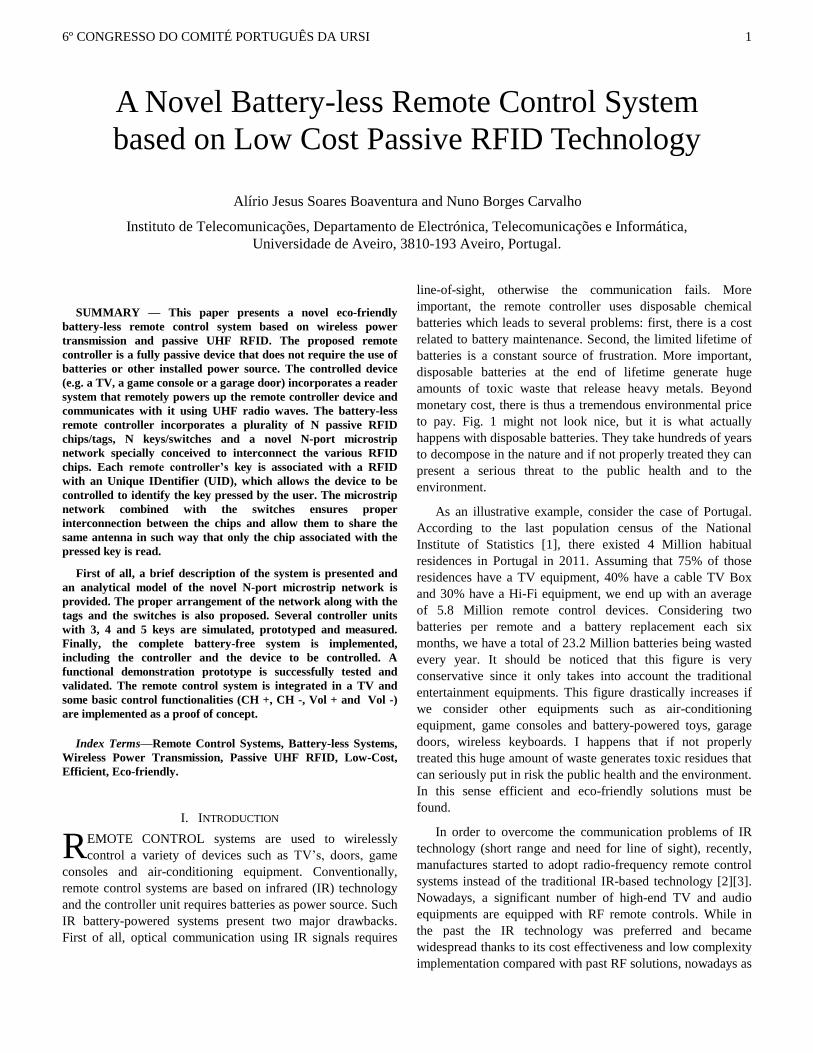
Fig. 9 Measured input impedance of the switch. Point A corresponds to the
closed position in which the switch has a predominant inductive behavior.
Point B corresponds to the open position in which the switch has a
predominant capacitive behavior.
Fig. 10 Series circuit formed by the series circuit (switch plus LC circuit) in
parallel with a 50Ω load. When the switch is closed the series circuit
resonates at 866.6Mhz imposing an approximate short circuit (point C).
When the switch is open the input impedance is approximately 50Ω (point
D).
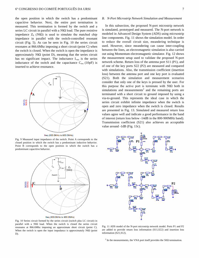
B. N-Port Microstrip Network Simulation and Measurement
In this subsection, the proposed N-port microstrip network
is simulated, prototyped and measured. The N-port network is
modeled in Advanced Design System (ADS) using micrsostrip
line components. Fig. 11 shows the simulation model. In order
to reduce the overall circuit size, meandering technique is
used. However, since meandering can cause inter-coupling
between the lines, an electromagnetic simulation is also carried
out using Momentum electromagnetic simulator. Fig. 12 shows
the measurement setup used to validate the proposed N-port
network scheme. Return loss of the antenna port S11 (P1), and
of one of the key ports S22 (P2) are measured and compared
with simulations. Also, the transmission coefficient (insertion
loss) between the antenna port and one key port is evaluated
(S21). Both the simulation and measurement scenarios
consider that only one of the keys is pressed by the user. For
this purpose the active port is terminate with 50Ω both in
simulations and measurements2 and the remaining ports are
terminated with a short circuit to ground imposed by using a
via-to-ground. This represents the ideal case in which the
series circuit exhibit infinite impedance when the switch is
open and zero impedance when the switch is closed. Results
are presented in Fig. 13. Simulated and measured return loss
values agree well and indicate a good performance in the band
of interest (return loss below -14dB in the 800-900MHz band).
Transmission coefficient (S21) also achieves an acceptable
value around -1dB (Fig. 13c).
Fig. 11 ADS model of the N-port microstrip network model. Ports P1 and P2
are added to provide return loss information (S11,S22) and insertion loss
information (S21,S12).
2 In the measurements, the VNA port itself provides the 50Ω termination.
A
B
C
D
P1
P2

6º CONGRESSO DO COMITÉ PORTUGUÊS DA URSI 8
Fig. 12 Measurement setup used to validate the proposed N-port network
scheme. The circuit is fabricated in low cost FR4 substrate in a 50Ω
environment. Antenna port and one of the key ports are probed in order to
evaluate the return loss and transmission coefficient. All other ports are short-
circuited to ground in order to simulate the inactive port condition.
(a)
(b)
(c)
Fig. 13 N-port network simulations (solid line) and measurement (circles): a)
return loss of port 1, b) return loss of port 2 and c) insertion loss between port
2 and port 1.
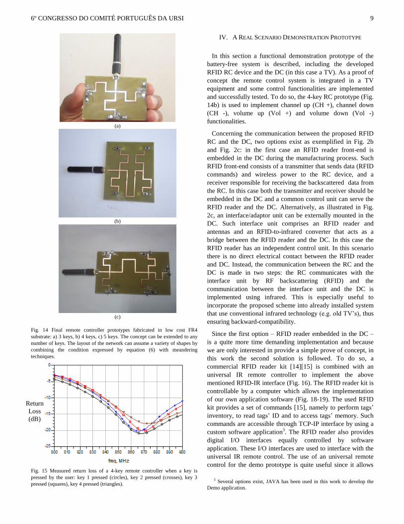
C. Final prototypes and measurements
The aim of this subsection is to prototype and measure the
complete RFID RC circuit. For this purpose, several RC
circuits with 3, 4 and 5 keys are simulated and prototyped. Fig.
14 shows the final prototypes of a 3-key, 4-key and 5-key
remote control units. Nevertheless, the proposed concept can
be extended to any number of keys simply by designing the
adequate N-port network. Moreover, the layout of the network
can assume a variety of shapes by using the degrees of
freedom expressed by equation (6) combined with meandering
techniques. This allows to place the keys in the desired
physical location of the board.
In order to simulate the entire RC circuit, the model of the N-
port network and the extracted/measured models of the RFID
chips and switches are used. In the measurements a 4-key RC
(Fig. 14b) is connected to the VNA in order to evaluate the
return loss of the controller when each key is pressed. It is
assumed that only one key is pressed each time. The VNA is
connected to the RC antenna port. The results depicted in Fig.
15 indicate good performance in the band of interest. These
measurements validate the previous mathematical formulation
of section II and the simulation results of previous subsection.
Only one RFID chip is active and routed to the antenna port
and the other chips remain in idle mode and do not interfere
with the active one.
P1
P2 via-to-ground
via-to-ground via-to-ground
via-to-ground
6º CONGRESSO DO COMITÉ PORTUGUÊS DA URSI 9
(a)
(b)
(c)
Fig. 14 Final remote controller prototypes fabricated in low cost FR4
substrate: a) 3 keys, b) 4 keys, c) 5 keys. The concept can be extended to any
number of keys. The layout of the network can assume a variety of shapes by
combining the condition expressed by equation (6) with meandering
techniques.
Fig. 15 Measured return loss of a 4-key remote controller when a key is
pressed by the user: key 1 pressed (circles), key 2 pressed (crosses), key 3
pressed (squares), key 4 pressed (triangles).
IV. A REAL SCENARIO DEMONSTRATION PROTOTYPE
In this section a functional demonstration prototype of the
battery-free system is described, including the developed
RFID RC device and the DC (in this case a TV). As a proof of
concept the remote control system is integrated in a TV
equipment and some control functionalities are implemented
and successfully tested. To do so, the 4-key RC prototype (Fig.
14b) is used to implement channel up (CH +), channel down
(CH -), volume up (Vol +) and volume down (Vol -)
functionalities.
Concerning the communication between the proposed RFID
RC and the DC, two options exist as exemplified in Fig. 2b
and Fig. 2c: in the first case an RFID reader front-end is
embedded in the DC during the manufacturing process. Such
RFID front-end consists of a transmitter that sends data (RFID
commands) and wireless power to the RC device, and a
receiver responsible for receiving the backscattered data from
the RC. In this case both the transmitter and receiver should be
embedded in the DC and a common control unit can serve the
RFID reader and the DC. Alternatively, as illustrated in Fig.
2c, an interface/adaptor unit can be externally mounted in the
DC. Such interface unit comprises an RFID reader and
antennas and an RFID-to-infrared converter that acts as a
bridge between the RFID reader and the DC. In this case the
RFID reader has an independent control unit. In this scenario
there is no direct electrical contact between the RFID reader
and DC. Instead, the communication between the RC and the
DC is made in two steps: the RC communicates with the
interface unit by RF backscattering (RFID) and the
communication between the interface unit and the DC is
implemented using infrared. This is especially useful to
incorporate the proposed scheme into already installed system
that use conventional infrared technology (e.g. old TV’s), thus
ensuring backward-compatibility.
Since the first option – RFID reader embedded in the DC –
is a quite more time demanding implementation and because
we are only interested in provide a simple prove of concept, in
this work the second solution is followed. To do so, a
commercial RFID reader kit [14][15] is combined with an
universal IR remote controller to implement the above
mentioned RFID-IR interface (Fig. 16). The RFID reader kit is
controllable by a computer which allows the implementation
of our own application software (Fig. 18-19). The used RFID
kit provides a set of commands [15], namely to perform tags’
inventory, to read tags’ ID and to access tags’ memory. Such
commands are accessible through TCP-IP interface by using a
custom software application3. The RFID reader also provides
digital I/O interfaces equally controlled by software
application. These I/O interfaces are used to interface with the
universal IR remote control. The use of an universal remote
control for the demo prototype is quite useful since it allows
3 Several options exist, JAVA has been used in this work to develop the
Demo application.
Return
Loss
(dB)

6º CONGRESSO DO COMITÉ PORTUGUÊS DA URSI 10
the prototype to be adaptable to any equipment covered by the
universal remote control.
The flowchart of the developed demo application is shown
in Fig. 19: the JAVA application sets the RFID reader to be
continuously scanning its field searching for RFID tags. Once
a tag is read, the application determines whether the read ID is
valid or not. If it is a valid key ID then the application
activates the corresponding key in the universal IR remote
controller through the reader I/O interface. The universal IR
remote controller is placed in the proximity of the equipment
to be controlled, allowing line-of-sight IR communication
between the RFID-IR interface and the TV.
Fig. 16 shows the complete transmitter/receiver setup
including a TV, a commercial RFID reader and antennas, a
computer running the demo application software and a
universal IR remote control. Details of the RFID-IR interface
are depicted in Fig. 17, precisely the universal IR controller
can be observed. In Fig. 18 is depicted the developed software
interface. The application allows the configuration of the RFID
reader (e.g. set output power level, start and stop scanning the
field), displays the ID’s of the tags being read by the reader
and also provides information of the control actions being
performed (CH-,CH+,VOL-, VOL+).
Fig. 16 Demonstration prototype of the complete battery-free remote control
receiver using an external RFID-IR interface unit: 1 – TV, 2 – RFID reader, 3
– reader antennas, 4 – RFID-IR interface and universal IR remote control,
detailed in the next figure, 5 – computer running application. In a final
industrial implementation all the external hardware (RFID reader and
antennas) would be miniaturized and integrated in the TV equipment. The
control software, now running in a computer, would be implemented in the
TV control unit.
Fig. 17 RFID-IR interface including a universal IR remote controller. In this
prototype it acts as a bridge between the RFID reader and the TV: it receives
information from the reader via a digital I/O interface and it sends this
information to the TV via IR signals.
Fig. 18 Demo application software that controls the RFID reader. In this case
the channel up icon is red indicating that the corresponding key is being
pressed in remote controller.
SET TCP-IP Connection
(Connect to RFID reader)
INIT RFID Reader
CONFIGURE Reader
(e.g. SET Output power level)
SCAN Reader’s Filed
IS THERE A TAG
IN THE FIELD?
NO
YES
READ Tag
(Access Tag ID)
VALID Key-ID?
YES
NO
DISPLAY Info
(e.g. CH UP icon gets red)
SET I/O Port according
to read Key-ID
TV operation
is performed(CH+,CH-,
Vol+, Vol-)
Fig. 19 Simplified flowchart of the developed JAVA application software.
IR LED
Cable from the RFID reader
1
2
3 3
4
5
6º CONGRESSO DO COMITÉ PORTUGUÊS DA URSI 11
V. CONCLUSION
A battery-less remote control system has been proposed and
prototyped. Several versions of the control unit with 3, 4 and 5
keys have been fabricated. Nevertheless, the concept can be
extended to any number of keys. A complete prototype of the
battery-free remote control system has been implemented and
tested. The system has been integrated in a TV and, as a proof
of concept, four basic control functionalities were successfully
implemented: CH-,CH+,VOL- and VOL+. Although the
prototype has been tested with a TV equipment, this remote
control scheme can be applied to a variety of other systems
specially in scenarios where the use of batteries is undesirable.
The proposed approach is based on a commercially available
low cost RFID technology and can be integrated in old systems
that use conventional infrared technology. Moreover, the
remote controller unit can be manufactured at very low cost.
This makes the solution quite affordable and cost-effective.
The main drawback of the proposed approach is related to the
need of having the RFID reader always turned on. Future work
will focus on this issue by combining passive RFID with other
energy harvesting technologies. A strategy can be followed in
which the RFID reader is turned off by default. The
mechanical strain energy generated when the user presses a
key can be used to generate a beacon pulse solely to wake up
the RFID reader while further communication is still made by
backscattering (RFID) mechanism as proposed in this work.
ACKNOWLEDGMENT
The authors would like to thank Portuguese Science and
Technology Foundation (FCT) for the financial support
provided under Project PTDC/EEA-TEL/099646/2008
TACCS.
First Author would like to thank FCT for the doctoral
scholarship SFRH/ BD/ 80615/ 2011
REFERENCES
[1] www.ine.pt, INE – Censos 2011
[2] Introducing ZigBee RF4CE,
http://www.daintree.net/downloads/whitepapers/zigbee-rf4ce-intro.pdf
[3] Texas Instruments, ZigBee RF4CE,
www.ti.com/ww/en/analog/bluetooth/zigbee_4_jan12.pdf
[4] Finkenzeller, Klaus, RFID Handbook, 2nd Edition ed. Wiley
[5] Daniel M. Dobkin, The RF in RFID: Passive UHF in Practice
[6] EPC Radio-Frequency Identity Protocols Class-1 Generation-2 UHF
RFID, Protocol for Communications at 860 MHz – 960 MHz, Version
1.2.0
[7] Swarup Mumar Mohalik, Method and Apparatus for Tag Activation,
United States Patent, US2007152828A1, Jul 2006
[8] William R. Sweeney, Controlable RFID Card, United Stated Patent
US2006187040A1, Feb. 2005
[9] Alírio J.S. Boaventura and Nuno B. Carvalho, Controlo Remoto Passivo
RFID e Sistema e Método de Compatibilização com a Tecnologia
Convencional. Patent application submitted to INPI – Intituto Nacional
de Propriedade Intelectual
[10] Pavel V. Nikitin, K. V. Seshagiri Rao, Rene Martinez, and Sander F.
Lam, “Sensitivity and Impedance Measurements of UHF RFID Chips”,
IEEE TRANSACTIONS ON MICROWAVE THEORY AND
TECHNIQUES, VOL. 57, NO. 5, MAY 2009
[11] Michael Hiebel, Fundamental of Vector Network Analysis,
RHODE&SCHWARZ
[12] Bourns, CHF1206CNT Series 20 W Power RF Chip Termination
[13] Rainer Kronberger, Alexander Geissler and Barbara Friedmann, “New
Methods to determine the Impedance of UHF RFID Chips”, IEEE
RFID 2010
[14] Alien technology, Hardware Setup Guide ALR-8800
[15] Alien technology, Reader Interface Guide, September 2007
Alírio Soares Boaventura was born in Cape Verde in 1985. He received
the Master degree in Electronics and
Telecommunication Engineering from the
University of Aveiro, Portugal, in 2009. From
2008 to 2010 his was with Acronym-IT, a
Portuguese manufacturing company devoted to
RFID, WSN and consumer electronics. In 2010
he joined the Institute of Telecommunications,
Aveiro, as a researcher and currently he is a PhD
student at the University of Aveiro. His main
research interests include passive RFID and
sensors, low power wireless systems, wireless
power transmission and energy harvesting, and CAD/Modeling for RFID.
From 2004 to 2009, Alírio received a merit scholarship for graduation from
the Gulbenkian Foundation. In 2011 Alírio Boaventura was a finalist of the
Student Paper Competition of the IEEE-International Microwave
Symposium. Recently, Alírio was the ex-aequo recipient of the 2011
URSI/ANACOM Prize, awarded by URSI-Portugal section and ANACOM.
Alírio is co-inventor of a patent and the author and co-author of a book
chapter and several articles in international conferences and journals. Alírio
Boaventura has also served as invited reviewer for the IEEE Transactions
on Microwave Theory and Techniques (TMTT) and the IEEE Journal on
Emerging and Selected Topics in Circuits and Systems (JETCAS).
Nuno Borges Carvalho, was born in Luanda in 1972. He received the
diploma and doctoral degrees in Electronics and
Telecommunications Engineering from the
Universidade de Aveiro, Aveiro, Portugal in
1995 and 2000 respectively. He is an Associate
Professor with “Agregação” at the same
University, and a Senior Research Scientist at
the Instituto de Telecomunicações. His main
research interests include CAD for nonlinear
circuits/systems, nonlinear distortion analysis in
microwave/wireless circuits and systems and
measurement of nonlinear phenomena, recently
he has also been involved in design of dedicated radios and systems for newly
emerging wireless technologies. He was the recipient of the 1995 University
of Aveiro and the Portuguese Engineering Association Prize for the best 1995
student at the Universidade de Aveiro, the 1998 Student Paper Competition
(third place) presented at the IEEE International Microwave Symposium, the
2000 IEE Measurement Prize. He is also the co-inventor of four registered
patents. He is a reviewer and author of more than 100 papers in several
magazines and conferences and the vice-chair of the IEEE MTT-11 Technical
Committee and the chair of the URSI-Portugal Metrology group. Dr. Borges
Carvalho is co-author of the book “Intermodulation in Microwave and
Wireless Circuits” from Artech House, 2003.