a novel ultra low power, high impedance current mirror...
TRANSCRIPT

International Journal of New Innovations in Engineering and Technology (IJNIET)
Vol. 1 Issue 3 February 2013 93 ISSN: 2319-6319
A Novel Ultra Low Power, High Impedance
Current Mirror Circuit for Biasing Operational
Amplifier in Sub-threshold Region
Anu Gupta
Birla Institute of Technology and Science, Pilani, India
Raj Singh Dua
Birla Institute of Technology and Science, Pilani, India
Abstract - In this paper, we propose MOSFET model in region II (saturation) of a subthreshold region (where
current becomes nearly constant with respect to drain-source voltage for a fixed gate-source voltage as shown in
figure 1). We also propose designs of current mirrors operating in region II of subthreshold region for biomedical
applications circuits like pacemakers, retinal implants, neural recording systems which are to be implanted within
chest, eye and skull respectively. These circuits also find use in emerging electronics devices such as palmtops, laptops
etc. The most important property of these circuits is extremely low power consumption in order to increase battery
life time yet it has structural simplicity. The proposed current mirror has a power dissipation ranging from 4nW to
1000nW for an input current ranging from 1nA to 250nA. Its output resistance is found to be of the order of 108 Ω to
1010 Ω. The minimum source voltage (V_dd or V_source) required to bias the proposed mirror varies between 550
mV to 875mV for the input current varying between 1nA to 250nA with W/L RATIO of all MOS transistors being
kept at 1. The minimum source voltage required further decreases if we increase W/L RATIO of MOS transistors.
The current mirror shows extremely low temperature sensitivity of 0.031ppm/degree C and it has a very high
resistance to source voltage fluctuations in comparison to the best current mirror circuits reported till date. The
operations of the current mirror have been validated through simulations in Cadence using 180nm TAIWAN
SEMICONDUCTOR MANUFACTURING COMPANY (TSMC) technology. The purpose of this paper is to model a
MOSFET in region II of the subthreshold region and to use that model to show that a topologically simple current
mirror designed in the subthreshold region works better than highly complex, saturation region current mirrors in
terms of output resistance, matching accuracy and variation with temperature.
I. INTRODUCTION
The equation of current in the subthreshold exponential region (i.e. region I as shown in figure 1) is given as
I_d = IoS expk(V_gs/V_th) exp(1-k)(V_bs/V_th) (1-exp-V_ds/V_th) (1)
Where V_th = KT/q is the thermal voltage, Io is a positive constant current, S is the transistor size factor (S =
W/L RATIO, where W is the transistor width and L is its length), k is a technology dependent positive
parameter, V_gs is the gate to source voltage, V_bs is the body (or bulk) to source voltage and V_ds is the drain
to source voltage [1]. In the circuit the V_gs and V_ds values were made same for M3 and M2, thus causing
I_out equal to I_in.
Figure 1 shows a variation of I_d with V_ds and equation 1 gives the variation of current (I_d) with V_ds in
region I. In this paper we propose a current mirror in which all the MOSFETs are biased in region II (saturation)
of subthreshold region thus making it an ultra low power current mirror.
This paper has been divided into 7 sections. Section 2 gives the overview of the characteristics of a typical
current mirror and schematic & performance parameters of the proposed current mirror. A MOS transistor
operating in the subthreshold region has been characterized in section 3. Section 4 gives details of the design of
the current reference in the subthreshold region. Section 5 gives the simulation results of the current mirror
while sections 6 and 7 give the conclusions and references, respectively.
II. CHARACTERISTICS OF TYPICAL CURRENT MIRROR CIRCUITS
2.1 Typical Current mirror circuits
Figure 2 shows the traditional current mirror. Since the output impedance of the traditional current mirror is not
infinite, the variation of the output node voltage V_ds (or the supply voltage) will influence the output current
I_out. The sensitivity of I_out to variations in V_ds is a drawback in the applications of the current mirror

International Journal of New Innovations in Engineering and Technology (IJNIET)
Vol. 1 Issue 3 February 2013 94 ISSN: 2319-6319
circuits. Also the output current is not exactly equal to input current due to λV_ds (λ-channel length modulation
parameter) mismatch in transistors M1 and M2.
The cascoded current mirror was proposed to increase the output impedance and improve the current transfer
ratio (i.e. the ratio of output current to input current). Even though this mirror improves output impedance and
has a good current transfer ratio, the output voltage swing (or the minimum required source voltage is increased)
is reduced due to the stacking of transistors.
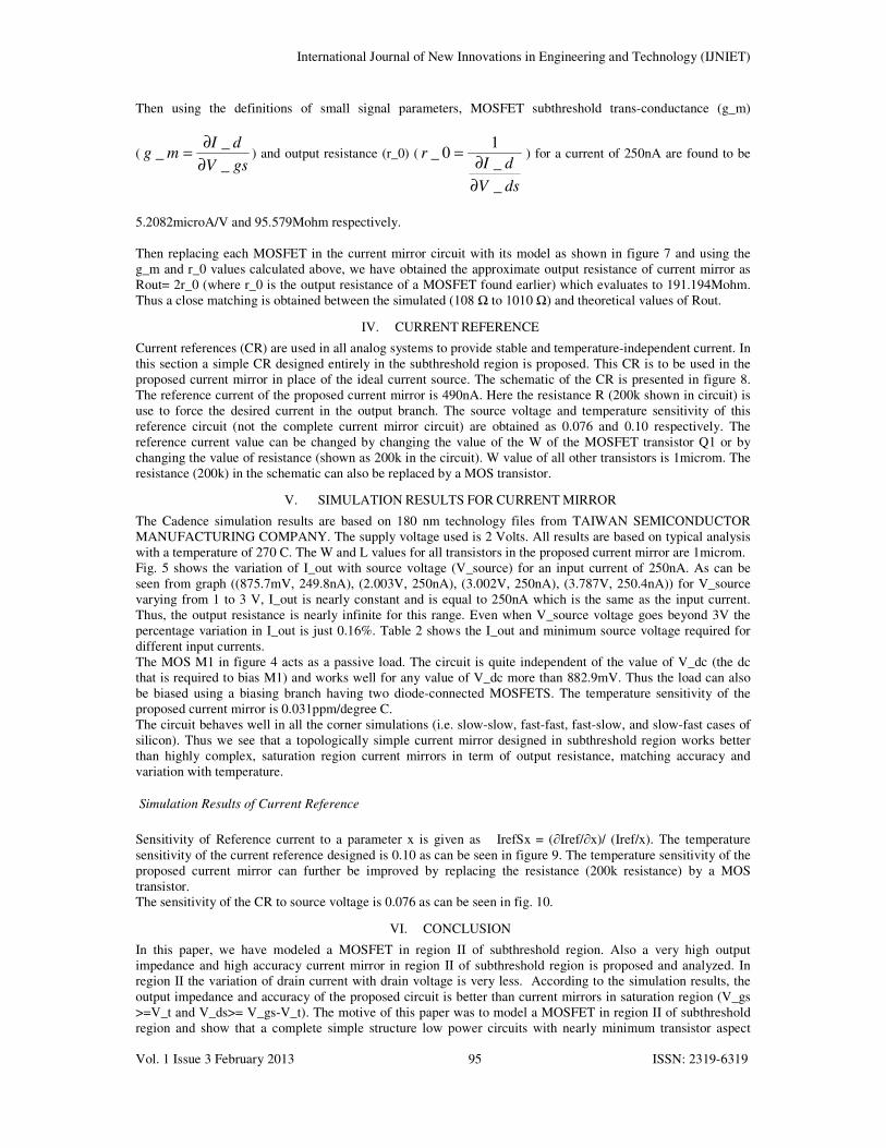
The current mirror shown in Fig.3 shows increased output impedance and better current transfer ratio as shown
by Kuo-Hsing Cheng, Chi-Che Chen and Chun-Fu Chung in “Accurate current mirror with high output
impedance” [2]. Although this current mirror has high output impedance and matches output current to input
current to a great extent, it also consumes a lot of power and occupies a large silicon area making it unsuitable
for use in low power circuits.
2.2 Proposed current mirror
The schematic of the proposed current mirror is shown in Fig.4. The complete circuit operates in the
subthreshold region and has a very simple structure. It also uses less number of MOS transistors thus occupying
minimum silicon area. The MOS transistors M2 and M3 are used for current mirroring operation. M4 and M5
are used to match the V_ds (drain to source voltage) of M2 and M3 in order to avoid Lambda effect and have
better current matching accuracy than a circuit with lambda effect. M1 simply acts as a passive load.
Since the subthreshold currents are very small, the V_dd or the source voltage required is very small (generally
less than 1 volt). From simulations, the observed power dissipated in the circuit is in the range of 4nW to
1000nW (it varies with the current to be mirrored). Since the output current varies negligibly with the output
voltage the output resistance is very high (figure 5), of the order of 108 Ω to 1010 Ω (These values were
calculated by taking ratio of instantaneous values of drain to source voltage V_ds to drain current I_d and then
taking average of these values for different V_ds, I_d and V_gs values). The output resistance values were
determined by taking the average of three V_ds by I_d values measured for a particular output current. The
minimum source voltage (V_dd) required to bias the proposed mirror varies between 550 mV to 875mV for the
input current varying between 1nA to 250nA with W/L RATIO of all MOSFET transistors kept at 1. These
values were measured by varying the V_dd and measuring the V_dd at which the output current came within
10% of the input current.
The minimum source voltage required further decreases if we increase W/L RATIO of MOSFETs. The current
mirror shows extremely low temperature sensitivity of 0.031ppm/degree C and it has a very high resistance to
voltage fluctuations required to bias the load in comparison to best current mirror circuits reported till date. All
simulation results are discussed in detail in section 5 of this paper.
For matched transistors, current transfer ratio is 1 even with a wide variation of power supply voltage. M1 can
also be biased using two diode connected MOS transistors. Also all the PMOS can be replaced by NMOS to get
a NMOS current mirror.
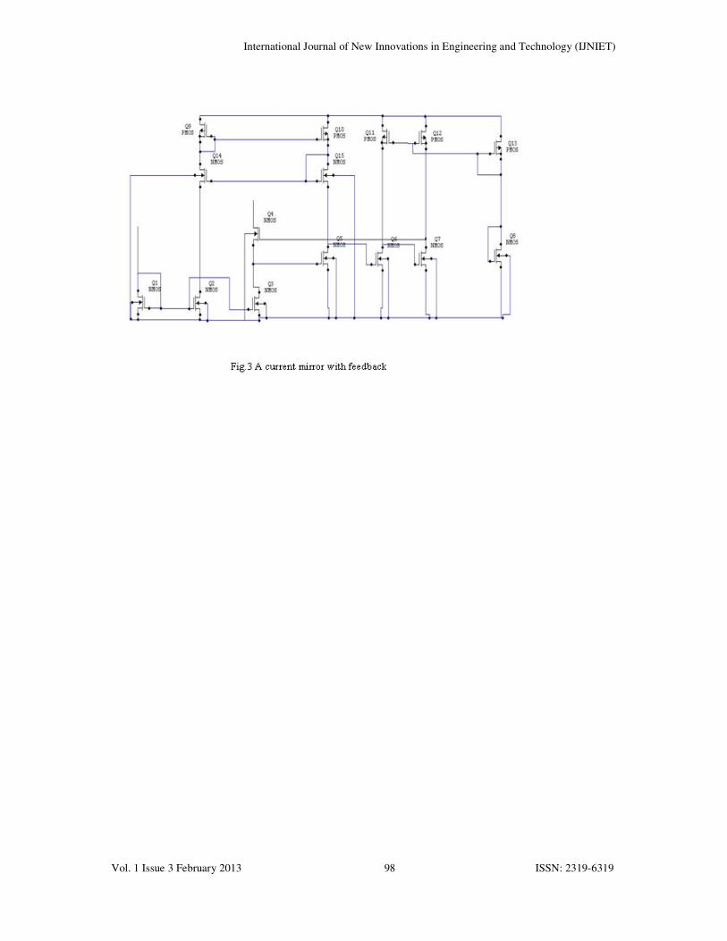
III. BEHAVIOR AND MODELING OF A MOSFET IN THE SUBTHRESHOLD REGION
In order to validate our simulated value of output resistance of the proposed current mirror circuit, we have
obtained the value theoretically using small signal analysis.
Since in our proposed current mirror circuit, MOSFETS M2, M3, M4 and M5 operate in region II (saturation)
where the dynamic resistance is high, we have interpolated the current-voltage relation (equation 1 which is
defined for region I) in this region using Newton’s Divided Difference technique (to get equation 2 for region II)
(We took the I_d values for 2 values of V_ds and found a and b and then took three such a and b values for three
V_gs and took their average). The circuit used to collect data for this interpolation is shown in figure 6. We have
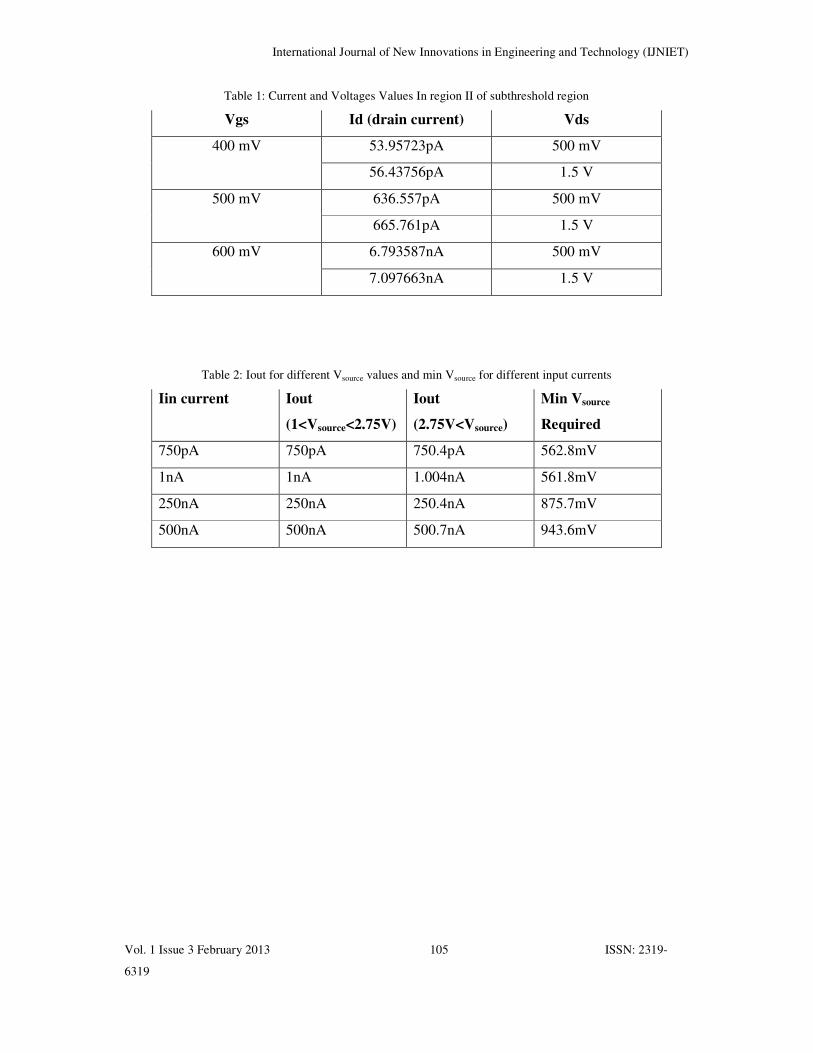
tabulated the data of the MOSFET of figure 6 that is biased in region II of subthreshold in Table 1.
Using the data given in Table 1, the subthreshold current equation in region II is modeled as
I_d= PexpkV_gs/V_th
(a+bV_ds) (2)
The exponential factor has been kept to consider the exponential dependence of current on V_gs. Here P=
I0Sexp(1-k)(V_bs/V_th), b and a are constants. In equation 2 we have neglected the exponential dependence of
current on V_ds as for large V_ds (in region II) 1-e-V_ds/V_th is nearly 1. In equation 1 if we neglect the V_ds
term we get I_ds= PexpkV_gs/V_th, from here we get equation 2 by interpolating this equation in region II
(saturation) of subthreshold region. More accurate models can be obtained by interpolating equation 2 to higher
degrees of V_ds. We solved equation 2 for values of a and b using Newton’s divided difference method for
three different values of V_gs and then took an average of the three values of a, b. The values of a, b obtained
are 0.89887 and 0.04185 Volt-1 respectively.
International Journal of New Innovations in Engineering and Technology (IJNIET)
Vol. 1 Issue 3 February 2013 95 ISSN: 2319-6319
Then using the definitions of small signal parameters, MOSFET subthreshold trans-conductance (g_m)
(gsV
dImg
_
__
∂
∂= ) and output resistance (r_0) (
dsV
dIr
_
_
10_
∂
∂= ) for a current of 250nA are found to be
5.2082microA/V and 95.579Mohm respectively.
Then replacing each MOSFET in the current mirror circuit with its model as shown in figure 7 and using the
g_m and r_0 values calculated above, we have obtained the approximate output resistance of current mirror as
Rout= 2r_0 (where r_0 is the output resistance of a MOSFET found earlier) which evaluates to 191.194Mohm.
Thus a close matching is obtained between the simulated (108 Ω to 1010 Ω) and theoretical values of Rout.
IV. CURRENT REFERENCE
Current references (CR) are used in all analog systems to provide stable and temperature-independent current. In
this section a simple CR designed entirely in the subthreshold region is proposed. This CR is to be used in the
proposed current mirror in place of the ideal current source. The schematic of the CR is presented in figure 8.
The reference current of the proposed current mirror is 490nA. Here the resistance R (200k shown in circuit) is
use to force the desired current in the output branch. The source voltage and temperature sensitivity of this
reference circuit (not the complete current mirror circuit) are obtained as 0.076 and 0.10 respectively. The
reference current value can be changed by changing the value of the W of the MOSFET transistor Q1 or by
changing the value of resistance (shown as 200k in the circuit). W value of all other transistors is 1microm. The
resistance (200k) in the schematic can also be replaced by a MOS transistor.
V. SIMULATION RESULTS FOR CURRENT MIRROR
The Cadence simulation results are based on 180 nm technology files from TAIWAN SEMICONDUCTOR
MANUFACTURING COMPANY. The supply voltage used is 2 Volts. All results are based on typical analysis
with a temperature of 270 C. The W and L values for all transistors in the proposed current mirror are 1microm.
Fig. 5 shows the variation of I_out with source voltage (V_source) for an input current of 250nA. As can be
seen from graph ((875.7mV, 249.8nA), (2.003V, 250nA), (3.002V, 250nA), (3.787V, 250.4nA)) for V_source
varying from 1 to 3 V, I_out is nearly constant and is equal to 250nA which is the same as the input current.
Thus, the output resistance is nearly infinite for this range. Even when V_source voltage goes beyond 3V the
percentage variation in I_out is just 0.16%. Table 2 shows the I_out and minimum source voltage required for
different input currents.
The MOS M1 in figure 4 acts as a passive load. The circuit is quite independent of the value of V_dc (the dc
that is required to bias M1) and works well for any value of V_dc more than 882.9mV. Thus the load can also
be biased using a biasing branch having two diode-connected MOSFETS. The temperature sensitivity of the
proposed current mirror is 0.031ppm/degree C.
The circuit behaves well in all the corner simulations (i.e. slow-slow, fast-fast, fast-slow, and slow-fast cases of
silicon). Thus we see that a topologically simple current mirror designed in subthreshold region works better
than highly complex, saturation region current mirrors in term of output resistance, matching accuracy and
variation with temperature.
Simulation Results of Current Reference
Sensitivity of Reference current to a parameter x is given as IrefSx = (∂Iref/∂x)/ (Iref/x). The temperature
sensitivity of the current reference designed is 0.10 as can be seen in figure 9. The temperature sensitivity of the
proposed current mirror can further be improved by replacing the resistance (200k resistance) by a MOS
transistor.
The sensitivity of the CR to source voltage is 0.076 as can be seen in fig. 10.
VI. CONCLUSION
In this paper, we have modeled a MOSFET in region II of subthreshold region. Also a very high output
impedance and high accuracy current mirror in region II of subthreshold region is proposed and analyzed. In
region II the variation of drain current with drain voltage is very less. According to the simulation results, the
output impedance and accuracy of the proposed circuit is better than current mirrors in saturation region (V_gs
>=V_t and V_ds>= V_gs-V_t). The motive of this paper was to model a MOSFET in region II of subthreshold
region and show that a complete simple structure low power circuits with nearly minimum transistor aspect

International Journal of New Innovations in Engineering and Technology (IJNIET)
Vol. 1 Issue 3 February 2013 96 ISSN: 2319-6319
ratios can be easily designed in subthreshold region of operation and they work better than complex circuits
designed for normal (with V_gs > V_t) region operation in terms of lower power consumption and smaller size
for the same output characteristics. The proposed current mirror, along with current reference circuit, is suitable
for use in extremely low power, high output impedance and low frequency operations. Such circuits are best
suited for bio-medical applications such as pacemakers, retinal implants, neural recording systems which are to
be implanted within chest, eye and skull respectively where power dissipation requirement has to be low to
increase battery life time.
REFERENCES
[1] Serrano-Gotarredona T., Linares-Barranco B. and Andreou A.G., A general subthreshold MOS translinear theorem, Proceedings of
the 1999 IEEE International Symposium on Circuits and Systems (ISCAS), Volume 2, (Jul 1999) 302 - 305.
[2] Kuo-Hsing Cheng, Chi-Che Chen and Chun-Fu Chung, Accurate current mirror with high output impedance, Proceedings of the 8th
IEEE International Conference on Electronics, Circuits and Systems (ICECS), 2001 Volume: 2, (2001) 565-568.
[3] Zeki A.; Kuntman H., Accurate and high output impedance current mirror suitable for CMOS current output stages, Electronics
Letters, Volume: 33 Issue: 12, (5 June 1997) 1042 -1043.
[4] J. Frenkil, A multi-level approach to low-power IC design, IEEE Spectrum, vol. 35, (1998) 54–60.
[5] B.Razavi, Design of Analog CMOS Integrated Circuits, Tata McGraw-Hill, 2002, New York.
[6] H.Soeleman and K.Roy, Ultra-low power digital subthreshold logic circuits, International Symposium Low Power Electronic Design, (1999)94–96.
[7] Gerald C. F.; Patrick O.W., Applied Numerical Analysis, Pearson Education Inc, New Delhi, 2007.
[8] H.Aziza, E.Bergeret and A. Perez, A novel Design Methodology for Current Reference Circuits, Proceedings of the 15th IEEE
International Conference on Electronics, Circuits and Systems (ICECS), (2008) 238-241.

International Journal of New Innovations in Engineering and Technology (IJNIET)
Vol. 1 Issue 3 February 2013 97 ISSN: 2319-6319
International Journal of New Innovations in Engineering and Technology (IJNIET)
Vol. 1 Issue 3 February 2013 98 ISSN: 2319-6319

International Journal of New Innovations in Engineering and Technology (IJNIET)
Vol. 1 Issue 3 February 2013 99 ISSN: 2319-6319

International Journal of New Innovations in Engineering and Technology (IJNIET)
Vol. 1 Issue 3 February 2013 100 ISSN: 2319-
6319

International Journal of New Innovations in Engineering and Technology (IJNIET)
Vol. 1 Issue 3 February 2013 101 ISSN: 2319-
6319

International Journal of New Innovations in Engineering and Technology (IJNIET)
Vol. 1 Issue 3 February 2013 102 ISSN: 2319-
6319

International Journal of New Innovations in Engineering and Technology (IJNIET)
Vol. 1 Issue 3 February 2013 103 ISSN: 2319-
6319
International Journal of New Innovations in Engineering and Technology (IJNIET)
Vol. 1 Issue 3 February 2013 104 ISSN: 2319-
6319
International Journal of New Innovations in Engineering and Technology (IJNIET)
Vol. 1 Issue 3 February 2013 105 ISSN: 2319-
6319
Table 1: Current and Voltages Values In region II of subthreshold region
Vgs Id (drain current) Vds
400 mV 53.95723pA 500 mV
56.43756pA 1.5 V
500 mV 636.557pA 500 mV
665.761pA 1.5 V
600 mV 6.793587nA 500 mV
7.097663nA 1.5 V
Table 2: Iout for different Vsource values and min Vsource for different input currents
Iin current Iout
(1<Vsource<2.75V)
Iout
(2.75V<Vsource)
Min Vsource
Required
750pA 750pA 750.4pA 562.8mV
1nA 1nA 1.004nA 561.8mV
250nA 250nA 250.4nA 875.7mV
500nA 500nA 500.7nA 943.6mV