a phonon scattering assisted injection and extraction based
TRANSCRIPT
LUND UNIVERSITY
PO Box 117221 00 Lund+46 46-222 00 00
A phonon scattering assisted injection and extraction based terahertz quantumcascade laser
Dupont, E.; Fathololoumi, S.; Wasilewski, Z. R.; Aers, G.; Laframboise, S. R.; Franckie,Martin; Razavipour, S. G.; Wacker, Andreas; Ban, D.; Liu, H. C.Published in:Applied Physics Reviews
DOI:10.1063/1.3702571
Published: 2012-01-01
Link to publication
Citation for published version (APA):Dupont, E., Fathololoumi, S., Wasilewski, Z. R., Aers, G., Laframboise, S. R., Franckie, M., ... Liu, H. C. (2012).A phonon scattering assisted injection and extraction based terahertz quantum cascade laser. Applied PhysicsReviews, 111(7), [73111]. DOI: 10.1063/1.3702571
General rightsCopyright and moral rights for the publications made accessible in the public portal are retained by the authorsand/or other copyright owners and it is a condition of accessing publications that users recognise and abide by thelegal requirements associated with these rights.
• Users may download and print one copy of any publication from the public portal for the purpose of privatestudy or research. • You may not further distribute the material or use it for any profit-making activity or commercial gain • You may freely distribute the URL identifying the publication in the public portal ?

A phonon scattering assisted injection and extraction based terahertzquantum cascade laserE. Dupont, S. Fathololoumi, Z. R. Wasilewski, G. Aers, S. R. Laframboise et al. Citation: J. Appl. Phys. 111, 073111 (2012); doi: 10.1063/1.3702571 View online: http://dx.doi.org/10.1063/1.3702571 View Table of Contents: http://jap.aip.org/resource/1/JAPIAU/v111/i7 Published by the American Institute of Physics. Related Articles1.3μm InAs/GaAs quantum dot lasers on Si substrates by low-resistivity, Au-free metal-mediated wafer bonding J. Appl. Phys. 112, 033107 (2012) Electronic tuning of integrated blue-violet GaN tunable coupled-cavity laser AIP Advances 2, 032130 (2012) Electrically pumped lasing from p-ZnO/n-GaN heterojunction diodes Appl. Phys. Lett. 101, 053503 (2012) A Thomson scattering diagnostic on the Pegasus Toroidal experiment Rev. Sci. Instrum. 83, 10E335 (2012) Electrically pumped lasing from single ZnO micro/nanowire and poly(3,4-ethylenedioxythiophene):poly(styrenexulfonate) hybrid heterostructures Appl. Phys. Lett. 101, 043119 (2012) Additional information on J. Appl. Phys.Journal Homepage: http://jap.aip.org/ Journal Information: http://jap.aip.org/about/about_the_journal Top downloads: http://jap.aip.org/features/most_downloaded Information for Authors: http://jap.aip.org/authors
Downloaded 08 Aug 2012 to 130.235.184.47. Redistribution subject to AIP license or copyright; see http://jap.aip.org/about/rights_and_permissions

A phonon scattering assisted injection and extraction based terahertzquantum cascade laser
E. Dupont,1,a) S. Fathololoumi,1,2 Z. R. Wasilewski,1 G. Aers,1 S. R. Laframboise,1
M. Lindskog,3 S. G. Razavipour,2 A. Wacker,3 D. Ban,2 and H. C. Liu4
1Institute for Microstructural Sciences, National Research Council, Ottawa, Ontario K1A0R6, Canada2Department of Electrical and Computer Engineering, Waterloo Institute of Nanotechnology,University of Waterloo, 200 University Ave W., Waterloo, Ontario N2L3G1, Canada3Division of Mathematical Physics, Lund University, Box 118, Lund 22100, Sweden4Key Laboratory of Artificial Structures and Quantum Control, Department of Physics, Shanghai JiaoTong University, Shanghai 200240, China
(Received 25 January 2012; accepted 6 March 2012; published online 12 April 2012)
A lasing scheme for terahertz quantum cascade lasers, based on consecutive phonon-photon-phonon
emissions per module, is proposed and experimentally demonstrated. The charge transport of
the proposed structure is modeled using a rate equation formalism. An optimization code based
on a genetic algorithm was developed to find a four-well design in the GaAs/Al0.25Ga0.75As
material system that maximizes the product of population inversion and oscillator strength at
150 K. The fabricated devices using Au double-metal waveguides show lasing at 3.2 THz up
to 138 K. The electrical characteristics display no sign of differential resistance drop at lasing
threshold, which, in conjunction with the low optical power of the device, suggest—thanks
to the rate equation model—a slow depopulation rate of the lower lasing state, a hypothesis
confirmed by non-equilibrium Green’s function calculations.
[http://dx.doi.org/10.1063/1.3702571]
I. INTRODUCTION
Nearly a decade after the first demonstration of terahertz
(THz) quantum cascade lasers (QCL),1 the maximum operat-
ing temperature (Tmax) of these devices has reached 199.5 K,
using a three-well resonant phonon design.2 The high tem-
perature THz-QCLs (Tmax & 175 K) are mostly designed
using resonant tunneling-based injection and extraction of
carriers from the lasing states in a GaAs/Al0.15Ga0.85As
material system.2–5 Despite the relatively slow progress on
improving the Tmax, research efforts remain very intense to
bring THz QCL into a temperature range achievable with
thermo-electric coolers. This would open up a profusion of
THz applications in many areas, including high speed com-
munications, pharmacology, non-invasive cross sectional
imaging, quality control, gas and pollution sensing, biochem-
ical label-free sensing, and security screening.6
Several theoretical models have been employed to
understand details of charge transport and optical gain in
THz QCLs, including density matrix formalism,7–9 non-
equilibrium Green’s function (NEGF),10–12 and Monte Carlo
techniques.13,14 These models have identified several limita-
tions of THz QCLs based on resonant tunneling injection
(RT-QCL), which make it difficult for the lasers with photon
energy �hx to operate at temperatures T > �hx=kB (kB being
the Boltzmann constant). It is therefore necessary to find
alternative designs with novel lasing schemes and/or investi-
gate materials with lower electron effective mass.15 In this
paper, we focus on the first approach.
Yasuda et al.,16 Kubis et al.,17 and Kumar et al.18 have
also pointed out the limitations of RT-QCL and examined a
family of designs for THz QCLs that was formerly proposed
with the terminology “indirect pump” scheme (IDP) and dem-
onstrated experimentally in mid-infrared devices by Yama-
nishi et al.19 In this scheme, carrier injection to the upper
lasing state (ULS, also called level 2) is assisted by longitudi-
nal optical (LO) phonon scattering, and is, hence, so-called
scattering-assisted QCL (SA-QCL) or, alternatively, IDP-
QCL. This type of lasing scheme has recently proven its capa-
bility to significantly surpass the empirical Tmax � �hx=kB li-
mitation of RT-QCL: Kumar et al. have demonstrated a four-
well GaAs/Al0.25Ga0.85As SA-QCL at 1.8 THz with
Tmax ¼ 163 K � 1:9�hx=kB.18 A design of IDP-QCL consist-
ing of five wells per module was also demonstrated at 4 THz
with Tmax � 47 K in the lattice-matched InGaAs-AlInAs-InP
material system.20 In the following, we propose a four-well
SA-QCL design, where the lower lasing state (LLS, also
called level 1) is depopulated via resonant phonon scattering,
but without the mediation of resonant tunneling. The proposed
design involves only four fairly confined states that are iso-
lated from higher energy levels.
We recall the main drawbacks faced by the RT-QCL.
The population inversion (DN/Ntot) in the QCLs based on
resonant tunneling for the injection is limited to 50%. This is
due to the direct pump scheme in such designs, i.e., to the ex-
istence of the injector level, i, where carriers wait to get reso-
nantly injected into the ULS. Ideally, in the coherent
transport regime, the ULS holds as many carriers as the in-
jector level, which is only half of the total available carriers.
In a realistic case, with rather thick injection barrier and
presence of scattering channels, the population inversiona)Electronic mail: [email protected].
0021-8979/2012/111(7)/073111/10/$30.00 111, 073111-1
JOURNAL OF APPLIED PHYSICS 111, 073111 (2012)
Downloaded 08 Aug 2012 to 130.235.184.47. Redistribution subject to AIP license or copyright; see http://jap.aip.org/about/rights_and_permissions

falls below 50%. Moreover, as the injector state is populated,
thermal backfilling to the lower lasing state (LLS) cannot be
ignored at high temperatures.16,21 It was also predicted that
the presence of injection and extraction tunneling couplings
broadens the gain with a complicated electric field depend-
ency,8,9,22,23 which makes it hard to predict the laser fre-
quency. In order to inject carriers selectively to the ULS and
not the LLS, the injection barrier should be chosen meticu-
lously: thick enough to avoid the counterproductive (also
called “wrong”) injection of carriers to the LLS as well as to
reduce the negative differential resistance (NDR) at the
i-LLS level alignment and, at the same time, thin enough to
increase the laser’s current density dynamic range. It is im-
portant to note that, due to the small ULS and LLS energy
spacing (small photon energy), the i-ULS and i-LLS level
alignments happen at similar electric fields. The diagonality
of the lasing transition was used as a design tool to decouple
the intermediate tunneling resonances and the injection reso-
nance, which occur before and at the design electric field,
respectively.4,24 The trade-off in designing the injection tun-
neling barrier is even harder to satisfy for devices with
smaller photon energy. As a consequence, the transport
across the injection barrier may not become completely
coherent, particularly when considering all existing scatter-
ing processes, and therefore the peak current becomes sensi-
tive to variations of dephasing scattering during tunneling.18
Cited here in chronological order, Refs. 16, 17, 18, and
19 provide comprehensive discussions of how SA-QCL
designs address the shortcomings of the RT-QCL. Figure 1
illustrates schematically the operation principle of the SA-
QCLs, with consecutive “phonon-photon-phonon” emissions
per module. In energy ascending order, the states are named
e (for extraction from LLS), 1, 2, and i (for injection to
ULS). Such design schemes rely on an injection energy state,
i, lying about one LO-phonon energy above the ULS. The
carriers are injected from the upstream extraction level, e0, to
the next injection level i by resonant tunneling. Since the
electric field at e0-i alignment is much larger than that for
e0-2 and e0-1 alignments, the injection resonance e0-i is well
decoupled from the last two resonances, and a large coupling
strength, Xei, can be used in the design. Therefore, it is possi-
ble to have thin tunneling barriers, while preserving the
pumping selectivity to the ULS, provided the diagonality
between the lasing states is adjusted to minimize the relaxa-
tion from i to 1. As a result, this type of design relies on a
large diagonality between lasing states; hence, the occur-
rence of photon emission–assisted tunneling through a rather
thick “radiative barrier”.18 By choosing a thin injection bar-
rier, i.e., a strong tunneling coupling strength, Xei, one can
ensure coherent transport and subsequent accumulation of
carriers on the state with longest lifetime—preferably the
ULS. Therefore, the indirect pump scheme can overcome the
50% limitation of the population inversion in RT-QCL.19
Subsequently, the large population inversion would result in
a small concentration of carriers on the short lifetime injec-
tion state i and its tunneling partner, the extractor state e0,which reduces the effect of backfilling to state 10. The strong
reduction of carrier concentration in the injector of mid-
infrared IDP-QCL was confirmed experimentally; it results
in a reduced backfilling of carriers to the LLS, as well as a
low optical absorption in the injector. All of the above proc-
esses contribute to the observed high T0, the characteristic
temperature of the threshold.19,25 Additionally, the coherent
transport through the barrier makes current and population
inversion relatively insensitive to variations of dephasing
processes.
As shown in Fig. 1, for depopulating the LLS, we pro-
pose to rely on LO-phonon emission scattering, an extraction
scheme already demonstrated in two-well RT-QCLs.23,26
Our design is analogous to the THz IDP-QCL theoretically
studied in Ref. 17, where the carrier thermalization is maxi-
mized within one period by adjusting the electrostatic poten-
tial per module to twice the LO-phonon energy.27
Alternatively, one could use the mediation of tunneling to an
excited state in resonance with LLS before LO-phonon emis-
sion scattering to the extraction state, a configuration that
could be named “phonon-photon-tunnel-phonon”.18,20 One
could also skip the depopulation by LO-phonon emission
and make the LLS act as a state that feeds the injection state
of the next module by resonant tunneling, an extraction-
controlled “phonon-photon” configuration, which offers the
advantage of a lower voltage defect.28
In this work, we focus on “phonon-photon-phonon”
scheme and evaluate the lasing states (and gain profile) that
are not perturbed by injection and/or extraction tunnelings.
In such a scheme, the relative diagonality between the four
states should be carefully adjusted to ensure fast injection to
ULS and extraction from LLS, while minimizing the wrong
injection i ! 1 and extraction 2 ! e channels and, at the
same time, maintaining a sufficient oscillator strength
between the lasing states. In Sec. II, we will discuss the key
figures of merit derived from rate equations and used for
design optimization.
II. RATE EQUATIONS
The key figures of merit, such as population inversion
and transit time of a “phonon-photon-phonon” design, can
be derived analytically from rate equations, thanks to the
operational simplicity of such SA-QCL designs. We denoteFIG. 1. Schematic diagram of a scattering assisted QCL active region based
on a “phonon-photon-phonon” configuration.
073111-2 Dupont et al. J. Appl. Phys. 111, 073111 (2012)
Downloaded 08 Aug 2012 to 130.235.184.47. Redistribution subject to AIP license or copyright; see http://jap.aip.org/about/rights_and_permissions
the scattering rate from state l to m as glm and the inverse of
glm as slm. The tunneling time across the injection barrier can
be written as stun ¼ ð1þ D2s2kÞ=2X2sk, where �hD and �hX
are, respectively, the detuning energy and tunneling coupling
strength between the states e and i and sk denotes the phase
coherence time constant.29 For the rate equation model, the
basis of states is taken from the eigenstates of “isolated mod-
ules”, as if the injection barrier were very thick. Simplified
analytical forms can be obtained when backscattering is
neglected (i.e., at low temperature): gml � glm, where
El>Em. The total down scattering rates from levels i and 2
are defined as gi¼ gi2þ gi1þ gie and g2¼ g21þ g2e, respec-
tively. For the sake of simplicity, we define g1¼ g1e. In the
absence of stimulated emission, i.e., below threshold
(J< Jth), the population inversion normalized to the total
number of carriers per period reads
Dq ¼ ~s2eff
stun þ s<tr; (1)
where ~s2eff is called the modified effective lifetime of ULS
and is defined as
~s2eff ¼gi2ðg1 � g21Þ � g2gi1
g1g2gi(2)
and s<tr is the transit time below threshold defined as
s<tr ¼gi2ðg1 þ g21Þ þ g2ð2g1 þ gi1Þ
g1g2gi: (3)
The normalized populations on states i and e can be written
simply as
qii ¼si
stun þ s<tr; (4)
qee ¼stun þ si
stun þ s<tr; (5)
respectively. The current density below threshold was calcu-
lated in the middle of the tunneling barrier. Assuming this
layer to be crossed only by tunneling currents, the current
density can be written simply as
J< ¼ qNs
qee � qii
stun
¼ qNs
stun þ s<tr; (6)
where Ns is the two-dimensional carrier density per module.
In the ideal case, where leakages gi1, gie, and g2e are negligi-
ble, the transit time and population inversion converge
toward intuitive expressions: s<tr � 2si2 þ s21 þ s1 and
Dq � ðs21 � s1Þ=ðstun þ s<tr Þ, respectively. If the inter-
subband relaxation time between the lasing states, s21, is
much longer than the injection and extraction lifetimes, and if
the tunneling time is much shorter than the transit time, the
population inversion could approach 100%. Equation (5) also
suggests that, to avoid accumulation of carriers behind the
tunneling barrier, the transport should be coherent (stun � si
or, equivalently, 2X2sksi � 1). We note that Eqs. (1)–(4) are
equivalent to those derived in Ref. 19 for IDP-QCL.
In the presence of stimulated emission (J> Jth), the pop-
ulation inversion is clamped at Dqth, which is fixed by the
cavity loss and the gain cross-section. Following the same
method as in Ref. 8, one can show that the current density
above threshold is
J> ¼ qNs
1� Dqthg1�g2e
g1þg2e
stun þ s>tr; (7)
where s>tr is the transit time above threshold and is approxi-
mately 4si, assuming efficient and analogous (gi2 � g1)
injection and depopulation rates. More precisely, the transit
time above threshold becomes
s>tr ¼ 2si 1þ gi2 þ gi1
g1 þ g2e
� �: (8)
The fractional change in differential resistance at threshold,
DRth/Rth, is also calculated as
DRth
Rth
¼ R<th � R>thR<th
¼ Dqth
g1 � g2e
g1 þ g2e: (9)
A discontinuity of differential resistance is expected at
threshold, as the current below threshold depends on the
intersubband relaxation between lasing state, s21 (see
Eq. (2)), and above threshold, this relaxation is governed
by stimulated emission. Implicitly, the Eqs. (6) and (7)
for the current density below and above threshold include
the electric field dependence on each term: stun, but also
s<tr , Dqth, s>tr , g1, and g2e. The Eq. (9) for the fractional
change in differential resistance was extracted by neglect-
ing the Stark effect; in other words, two assumptions
were used: (i) a voltage-independent population inversion
Dqth, i.e., a frequency independent resonator loss in con-
junction with a voltage-independent gain cross section, or
equivalently, a constant product between the lasing oscil-
lator strength and gain bandwidth and (ii) a low electric
field dependence of the transit times s<tr , s>tr , and the ratio
(g1� g2e)/(g1þ g2e). These assumptions may be too dras-
tic, especially when the lasing transition is highly diago-
nal; nevertheless, these expressions give important
guidelines.
From Eqs. (1), (6), and (7), the current density dynamic
range gives a condensed form of
Jmax
Jth
¼ 1� DRth=Rth
Dqth
2X2sk~s2eff
1þ 2X2sks>tr;
limcoh:trans:
Jmax
Jth
� �¼ 1� DRth=Rth
Dqth
~s2eff
s>tr:
(10)
The second expression shows the importance of using coher-
ent transport across the tunneling barrier in order to
maximize the dynamic range, a condition reached when
2X2sks>tr � 1 or approximatively when 8X2sksi � 1. The
differential internal efficiency of the laser is obtained as
g ¼ gi2ðg1 � g21Þ � g2gi1
giðg1 þ g2eÞ: (11)
073111-3 Dupont et al. J. Appl. Phys. 111, 073111 (2012)
Downloaded 08 Aug 2012 to 130.235.184.47. Redistribution subject to AIP license or copyright; see http://jap.aip.org/about/rights_and_permissions

If we define the effective lifetime of level 2 by the standard
expression, s2eff ¼ s2ð1� s1=s21Þ, more intuitive expres-
sions for the modified effective lifetime and the internal effi-
ciency can be obtained as
~s2eff ¼gi2
gis2eff �
gi1
gis1; (12)
g ¼ ~s2eff
s2eff þ s1
; (13)
respectively. Equation (12) shows how the effective ULS
lifetime is modified by the leakages channels i! 1 and i!e that are shunting the “correct” trajectory of carriers inside
a module from i! 2! 1! e. The fractional change in dif-
ferential resistance at threshold is closely related to the inter-
nal efficiency; it can be re-written versus s2eff as
DRth
Rth
¼ Dqth
s2eff þ s1g21�g2e
g2
s2eff þ s1
; (14)
an expression which shows similarities with Eq. (13). From
Eq. (9), it appears that the discontinuity in differential resist-
ance would vanish if the depopulation rate, g1, is inefficient
and close to the wrong depopulation channel, g1 � g2e.
Nevertheless, in such adverse conditions, population inver-
sion is still possible if the transition rate between lasing
states, g21, is lower than g21lim ¼ g2egi2�gie
gi2þgie. In this situation,
the modified effective lifetime, s2eff , would be small
� g21 lim � g21ð Þ=2g22e ðfor g21 . g21 limÞ, implying the effi-
ciency of the laser will be impeded. Of course, the transit
time above threshold would be much longer than 4si. In Sec.
III, we describe how the rate equation model was employed
to design the first iteration of SA-QCL based on the
“phonon-photon-phonon” scheme.
III. DESIGN OF STRUCTURE
Our first iteration of the “phonon-photon-phonon”
design optimized a figure of merit proportional to the gain
per number of carriers in a module. This figure of merit is
defined as the product of population inversion, oscillator
strength, and the inverse of the superperiod length. We chose
to maximize this figure of merit using four quantum wells in
the GaAs/Al0.25Ga0.75As material system at 21 kV/cm and a
lattice temperature of 150 K. We assumed a Maxwell-
Boltzmann distribution for the carriers in all subbands, with
a characteristic temperature of Te¼ 200 K. For the first itera-
tion, we assumed that transport is dominated by LO-phonon
scattering and neglected electron-impurity and interface
roughness (IR) scattering, which can be a serious shortcom-
ing. The calculation included both forward and backward
scattering channels. A more accurate figure of merit would
include several scattering potentials acting on the population
rate and dephasing of the lasing transition. To avoid leakage
channels to higher energy states, we deliberately opted for a
rather thick injection barrier of 44 A. Within this model, a
genetic algorithm–based optimization approach was used to
find the optimum thicknesses of four quantum wells and
three barriers (the injection tunneling barrier thickness being
fixed). The energy spacing between the four levels were
unbound during the optimization process.
The optimization resulted in the solution schematically
shown in Fig. 2 at 21 kV/cm. Starting from the injection bar-
rier, it consists of four wells and barriers with the layer thick-
nesses of 44/62.5/10.9/66.5/22.8/84.8/9.1/61 A—the barriers
are indicated in bold fonts. The injection barrier is delta-
doped with Si to 3.25 � 1010 cm�2 at the center. Interest-
ingly, with the discussed figure of merit, which only includes
LO-phonon scattering and the assumption of the same elec-
tronic temperature of 200 K in all subbands, the genetic algo-
rithm converged toward a low energy spacing between the
LLS and the extraction level, E1�Ee¼ 27.7 meV, i.e.,
9 meV lower than the bulk GaAs LO-phonon energy. This
suggests that, within our simplified model, the depopulation
rate is thermally activated (with a 9-meV activation energy),
which impedes population inversion at low temperature. The
electrostatic energy per module is 76 meV, i.e., approxi-
mately twice the phonon energy.17,27 With the choice of
thick injection barrier, the tunneling coupling strength is
rather weak (�hX¼ 1.14 meV), comparing with 1.5 meV from
the first demonstrated THz SA-QCL in Ref. 18.
In the conduction band diagram shown in Fig. 2 at
21 kV/cm, the four main wavefunctions are completely iso-
lated from higher energy states. For simplicity, when the
wavefunctions are solved for several modules (opposite case
to “isolated modules”) we keep the already discussed nota-
tion of states e, 1, 2, and i, even when the wavefunctions are
hybridized from a pair of states that are in resonance, like
levels e and i00 in Fig. 2. The optimization converged toward
excellent wavefunction overlaps between i-2 and 1-e, which
FIG. 2. Conduction band diagram and the moduli squared of wavefunctions
at 21 kV/cm of the designed THz QCL active region based on “phonon-pho-
ton-phonon” scheme. The “þ” signs denote the ionized impurities used for
doping. The LO-phonon emission–assisted scattering times sðLOÞlm are given
for the initial kinetic energy ELO � Elm.
073111-4 Dupont et al. J. Appl. Phys. 111, 073111 (2012)
Downloaded 08 Aug 2012 to 130.235.184.47. Redistribution subject to AIP license or copyright; see http://jap.aip.org/about/rights_and_permissions

led to short LO-phonon emission scattering times of 0.25 ps
for both transitions at initial kinetic energy ELO � Ei2,1e. The
thick “radiative barrier” (22.8 A) and the strong diagonality
between the lasing states lead to an oscillator strength of
0.39 at 3.46 THz and a LO-phonon emission scattering time
sðLOÞ21 �1.1 ps at 22.4 meV initial kinetic energy (ELO – E21).
Considering the high overlap between levels i-2 and between
1-e, this design behaves like a two-well structure. Since the
four wavefunctions are fairly diagonal to each other and iso-
lated from higher subbands, the free carrier absorption of the
active region is probably small.30 This type of design would
need to be experimentally optimized versus the doping den-
sity. Without the concern of free carrier absorption, the dop-
ing could be increased; for instance, electron-electron
scattering could favor carrier thermalization and potentially
improve device performance, but on the other hand,
e-impurity scattering could increase the gain linewidth, par-
ticularly at high temperatures.21 Even though the optimiza-
tion process was performed with only LO-phonon scattering,
the subsequent simulations include LO-phonon, IR, and
ionized impurity scattering potentials. For the sake of com-
parison, the scattering lifetimes of the six channels, shown in
Fig. 1, are listed in Table I. As expected, with the assumption
of Maxwell-Boltzmann carrier distributions, the total scatter-
ing time for depopulation, s1e, is shorter at elevated tempera-
tures, which is due to the 9-meV activation energy of LO-
phonon scattering. The IR scattering is expected to give a
large contribution between vertical states (i.e., i-2 and 1-e),
but we find it is also not negligible between the two diagonal
lasing states.17 The IR scattering contributes 71% (36%) to
the total scattering rate g21 at 20 K (150 K). In the next opti-
mization iteration, it would be important to include IR scat-
tering in the figure of merit. Several wafers based on this
simple design with different growth conditions could be
tested in order to elucidate the role of IR scattering in THz
QCL, a subject which is debated in the literature.11,12,31 A
more elaborate figure of merit could also include the gain
bandwidth, estimated by various scattering potentials (IR
scattering is likely to contribute the most).32,33 These refined
models would adjust the relative diagonality between the
four states. Table I shows that electron-impurity scattering
gives a small contribution.
The current density, optical gain, populations, and dif-
ferent characteristic lifetimes were calculated within the rate
equation model. The results versus electric field at two tem-
peratures (20 K and 150 K) are shown in Fig. 3. In the simu-
lation, the coherence time constant, sk, has a pure dephasing
time component, s*¼ 0.35 ps, which is assumed to be
temperature-independent for simplicity. The optical gain was
estimated by assuming a constant intersubband linewidth of
1 THz. The different lifetimes, as introduced in Sec. II, are
plotted in Fig. 3(a). We can see the tunneling time, stun, is
slightly shorter than the transit time above threshold, s>tr (by
a factor �2.8 at 20 K), meaning that the current dynamic
range is not optimized (see Eq. (10)). The tunneling time is
substantially longer than the injection state lifetime, si, by a
factor of 2, which indicates transport is not coherent through
the barrier. As a result, at the design electric field, the popu-
lations on the states e and i are very different. In other words,
carriers tend to accumulate on the extraction state and hence
promote backfilling to the LLS (see Eq. (5)). Figure 3(b)
illustrates the effect of backfilling on populations q11, qee,
and q22, particularly at electric fields below 21 kV/cm. At the
design electric field, the effect of backfilling at high
TABLE I. Scattering lifetimes (including LO-phonon, IR, and ionized im-
purity) in ps at 20 K and 150 K lattice temperatures. The IR scattering times
are calculated with a correlation length of KIR¼ 100 A and a mean rough-
ness height of DIR¼ 2 A. In the fourth column, e-impurity scattering times
are reported. In the last column, the total backscattering lifetimes at 150 K
are reported. Values are not reported for very long slm > 400 ps. In all sub-
bands, electrons were distributed according to Maxwell-Boltzmann statistics
with a temperature, Te, 50 K higher than lattice.
20 K 150 K
l – m slm sðIRÞlm sðimpÞlm slm sðIRÞlm sml
1-e 0.85 2.9 11.8 0.44 3.3 3.4
2-e 2.8 41.6 … 3 43.6 59.6
2-1 3 4.2 12.7 1.95 5.3 5.25
i-e 13.6 90 … 13 75 …
i-1 3 19.9 … 3.2 19.9 87
i-2 0.42 2.4 26.3 0.37 2.7 4.4
FIG. 3. Results of simulations based on the rate equation model performed
on the structure proposed in Fig. 2. (a) Different characteristic times at 20 K
(thick blue lines) and 150 K (thin red lines)—70 K and 200 K for electrons,
respectively. As discussed in Sec. II, stun is tunneling time (solid line), s<tr(dot line) and s>tr (dash dot line) are transit times before and after threshold;
si is injection state lifetime (dash line); s2eff is standard effective lifetime of
ULS (short dash line); and ~s2eff is modified effective lifetime (dash dot dot
line). (b) Normalized populations of the four states at 20 and 150 K lattice
temperatures. (c) Current density, lasing frequency, and optical gain vs elec-
tric field at 20 and 150 K lattice temperatures.
073111-5 Dupont et al. J. Appl. Phys. 111, 073111 (2012)
Downloaded 08 Aug 2012 to 130.235.184.47. Redistribution subject to AIP license or copyright; see http://jap.aip.org/about/rights_and_permissions

temperature is mitigated by the faster relaxation between
laser states s21 and depopulation s1e. At the design electric
field, the population of level i increases with temperature, as
the transit time s<tr for carriers contributing to current
decreases, while its lifetime remains unchanged. As shown
in Fig. 3(c), the slight decrease in current density at higher
temperature is related to backfilling to the LLS, meaning that
less carriers participate in the transport. We note that the op-
tical gain increases with the electric field at a slower pace
than the population inversion; this is due to the electric field
dependence of the oscillator strength, for instance, between
19 and 21 kV/cm, it changes from 0.472 to 0.392.
The peak gain value at 21 kV/cm was simulated versus
temperature, and the results are displayed in Fig. 4. Accord-
ing to the model presented in Sec. II, a peak gain value of
more than 40 cm�1 is maintained up to Te¼ 250 K. The sur-
prising rise of gain from low temperature up to Te¼ 110 K
originates from the assumption of Maxwell-Boltzmann dis-
tributions. This is due to the temperature-induced enhance-
ment of the depopulation rate (1 ! e) being greater than
that of the intersubband relaxation between the lasing states
(2! 1) at low temperatures. Indeed, the latter has an activa-
tion energy of 22.4 meV by LO-phonon scattering (versus
9 meV for g1e) and involves a pair of states that are more di-
agonal than the pair 1-e. Consequently, at low temperature,
g21 has a stronger contribution from IR scattering than g1e,
which is harder to change by LO-phonon scattering (see
Table I and right axis of Fig. 4). We can further see from
Fig. 4 that the temperature dependence of s21 – s1e and the
modified effective lifetime, ~s2eff , are mirrored in the gain. In
Sec. IV, we will describe the experimental results obtained
with the structure proposed in Fig. 2.
IV. EXPERIMENTAL RESULTS
The design presented in Fig. 2 was grown on a semi-
insulating GaAs substrate by molecular beam epitaxy with
276 repeats to obtain a 10 -lm-thick active region. The
active region was sandwiched between a bottom stack
100 nm of 3� 1018 cm�3 nþ GaAs followed by 20 nm of
non-intentionally doped GaAs spacer and a top stack of
8� 1017/5� 1018 cm�3 (40 nm/50 nm) nþ GaAs layers fol-
lowed by 10 nm of a 5� 1019 cm�3 nþ GaAs layer and
capped with 3 nm of low-temperature-grown GaAs. The
lower doping concentration of the bottom contact layer
(3� 1018 cm�3) and the 20-nm spacer were meant to limit
diffusion of Si dopants to the first period, which could induce
intermixing between the first layers of the active region.
Indeed, by transmission electron microscope imaging, we
observed blurred interfaces on the first three barriers of the
structures that were grown with 100 nm of 5� 1018 cm�3
bottom nþ GaAs followed by 10 nm of GaAs spacer.34
Special emphasis was put on minimizing the drift of fluxes
for Ga and Al during this long growth process. The x-ray dif-
fraction rocking curve could be fitted perfectly with nominal
parameters with no extra broadening of satellites peaks, con-
firming the excellent stability of the growth rates (better than
0.5%) throughout the active region. The wafers were
processed into THz QCL structures with Au double metal
waveguides. Devices have the following dimensions: �144 -
lm-wide ridges with �120 -lm-wide top Ti/Au metalli-
zation forming a Schottky contact and �1-mm-long
Fabry-Perot resonator. An In-Au wafer bonding technique
was used,35,36 and the ridges were fabricated by reactive-ion
etching. The laser bars were indium soldered (epi-layer side
up) on silicon carriers and then mounted in a He closed-
cycle cryostat for measurements.
Figure 5 shows the light (L)-voltage(V)-current density (J)
characteristics of the fabricated device from 10 K to 138 K in
pulsed mode, with pulse duration of 250 ns and repetition rate
of 1 kHz. The maximum collected power from this SA-QCL is
much lower than from a well-performing RT-QCL. The device
shows a Tmax of 138 K at a current density of 1.65 kA/cm2. At
10 K, the threshold current density is 1.17 kA/cm2 and the
maximum current density is 1.55 kA/cm2, resulting in a small
ratio of Jmax/Jth¼ 1.325. The laser action starts at 20.25 V and
FIG. 4. Left axis: peak gain at 21 kV/cm vs the electronic temperature from
simulations based on rate equation model. Right axis: intersubband recombi-
nation time between lasing states, s21, and depopulation time constant, s1e,
the difference s21 � s1e, and the modified effective lifetime of ULS, ~s2eff .
FIG. 5. Right axis: collected THz light (optical output power) vs current
density curves for Au double- metal THz QCLs based on the “phonon-pho-
ton-phonon” lasing scheme at different heat sink temperatures. Left axis:
voltage (V) vs current density (J) at 10 K and 130 K. The dashed horizontal
lines highlight the position of resonances in the V-J plot. The devices are
�144 -lm-wide, 1-mm-long, and are fabricated using TiAu metal contacts.
The bias is applied in pulsed mode (pulse width¼ 250 ns; repetition
rate¼ 1 kHz). The top inset shows a zoom of THz light and differential re-
sistance vs current density around threshold at 10 K. The bottom inset shows
the threshold density vs temperature.
073111-6 Dupont et al. J. Appl. Phys. 111, 073111 (2012)
Downloaded 08 Aug 2012 to 130.235.184.47. Redistribution subject to AIP license or copyright; see http://jap.aip.org/about/rights_and_permissions

stops at 21.8 V, where a NDR is observed. By subtracting the
Schottky voltage drop on the top contact (0.8 V),36 the NDR
voltage corresponds to the design electric field of 21 kV/cm. A
zoom-view of the differential resistance, Rac, versus current
density around threshold at 10 K (inset of Fig. 5) does not show
a clear discontinuity at threshold. Several measurements around
threshold with different voltage steps were attempted, but,
within the noise level of this pulsed measurement, no clear
change in the slope of the V-J characteristic could be
detected.37 The continuity of the differential resistance at
threshold was also observed at higher temperatures. According
to the rate equation model and its simplified solutions (Eq. (9)),
if we assume a resonator loss of 30 cm�1 and a gain bandwidth
of 1 THz, one expects a �6.4% drop of differential resistance
at threshold. By taking into account the electric field dependen-
cies of the oscillator strength and the scattering rates, this num-
ber raises to�11.6% for a threshold found at 19.45 kV/cm. The
noise level of the measured differential resistance is estimated
�8%, meaning that the detection of the expected�10% change
of Rac would be challenging. We propose that the vanishing dis-
continuity of differential resistance and the low output power of
the laser (proportional to the internal efficiency) are probably
related. The latter observation suggests that the effective life-
time of the ULS is much shorter than expected and conse-
quently reduces the internal efficiency of the laser (see
Eq. (13)). Analyzing the two observations together with the
model discussed in Sec. II suggests that the depopulation rate
1 ! e is not as efficient as expected. Moreover, according to
Eq. (10), the experimental ratio Jmax/Jth is an approximation of
~s2eff=Dqths>tr .
The slow rate of depopulation could be related to the
E1e energy spacing, being 9 meV smaller than the GaAs
LO-phonon energy. As the LO-phonon emission scattering
shows a strong resonance at initial kinetic energy ELO –
E1e, any deviation from the Maxwell-Boltzmann distribu-
tion could seriously alter the average depopulation rate
g1e—a crucial parameter for laser action. If thermalization
of carriers by e-e intrasubband scattering is not significantly
more efficient than intersubband scattering processes, the
carriers accumulate in the subband 1 up to the kinetic
energy of 9 meV, in contrast to the Fermi-Dirac or the
Maxwell-Boltzmann distributions.38,39 The relative sim-
plicity of this device would make it a good candidate for
studies of electron temperature by microprobe photolumi-
nescence experiments.40
At 10 K, the voltage versus current density plot shows a
tunneling resonance with a shoulder at �5.6 V and a strong
NDR region starting at 9.4 V and extending up to 17.6 V (left
axis on Fig. 5). Once the NDR region is crossed, the traces
of the current and voltage pulses are very clean and stable on
the oscilloscope. The same NDR region is observed at Tmax.
Taking into account the Schottky voltage drop on the top
contact (0.8 V), the electric field of these features correspond
well to the alignment of the extraction state e with levels 1and 2, predicted at 4.4 kV/cm and 8.7 kV/cm, respectively.
Figure 6 depicts the wavefunction configurations for these
electric fields. The anticrossing of the lasing states occurs at
13 kV/cm, implying that below 13 kV/cm level 2 (1) is
located on the downstream (upstream) side of the module. At
4.4 kV/cm, levels en�1 and 1 n are aligned with a coupling
strength of Xe1¼ 0.385 meV, while the next set of anti-
crossed states, en and 1 nþ1, are 16 meV below (qLe, e being
the electric field). It would suggest that the transition
1 n ! en is mainly assisted by IR scattering with a few ps
lifetime. At 20 K and for the e ! 1 tunneling transport,
4X2e1ske1s1 � 1, suggesting that transport is “in between” the
coherent and incoherent regimes. Interestingly, at the same
electric field, levels 2 nþ1 and inþ2 anticross and are also
aligned with 1 n and en�1. These four states could form a
weakly coupled miniband (see Fig. 6(a)). One could imagine
transport occurring two periods at a time from en�1 to 2 nþ1,
since 2qLe¼ 32 meV � ELO. Therefore, one can propose
that the shoulder in V-J plot at �5.6 V, which is also slightly
higher than the e�1 alignment voltage (4.4þ 0.8¼ 5.2 V),
corresponds to an electric field for which 2qLe � ELO
(4.8 kV/cm when taking into account the Schottky voltage
drop). At 8.7 kV/cm, levels en�1 and 2 n are aligned with a
small coupling strength Xe2¼ 0.24 meV. Transition to the
next lower extraction state en should be efficient, as
qLe¼ 32 meV � ELO. The figure of merit of e! 2 tunneling
transport is 4X2e2ske2s2 � 0:04� 1 at 20 K, suggesting that
this transport channel is incoherent and hence very depend-
ent on the phase coherence time constant.8,18
RT-QCLs with a small number of wells per module tend
to show large parasitic currents and sometimes pre-eminent
resonances in the V-J characteristic before threshold;4,24,26,41
this “quasi-two-well” SA-QCL confirms this phenomenon.
In order to raise the dynamic range, the coupling strength, X,
should be increased, but, with the present configuration, the
current due to parasitic resonances would drastically increase
as well. Several options to mitigate this latter effect exist,
including: (i) increasing the spatial separation between
wavefunctions of levels e and 2 (lower Xe2) by inserting
another well, lowering the design electric field while preserv-
ing the same oscillator strength, extraction mechanism, and
pump scheme to the next module;42 (ii) inserting one (or
more) well(s) between the extractor well and the injection
barrier, which results in a doublet (or a miniband) behind the
injection barrier that will selectively pump the injector state iof the downstream module. The latter strategy was adopted
in a THz IDP-QCL with a two-well extractor, where, even
with a large coupling strength, �hX � 4 meV, the V-J
FIG. 6. Conduction band diagram and the moduli squared of wavefunctions
at (a) 4.4 kV/cm and (b) 8.7 kV/cm.
073111-7 Dupont et al. J. Appl. Phys. 111, 073111 (2012)
Downloaded 08 Aug 2012 to 130.235.184.47. Redistribution subject to AIP license or copyright; see http://jap.aip.org/about/rights_and_permissions
characteristic of the devices did not show any sign of pump-
ing to the lower states.20
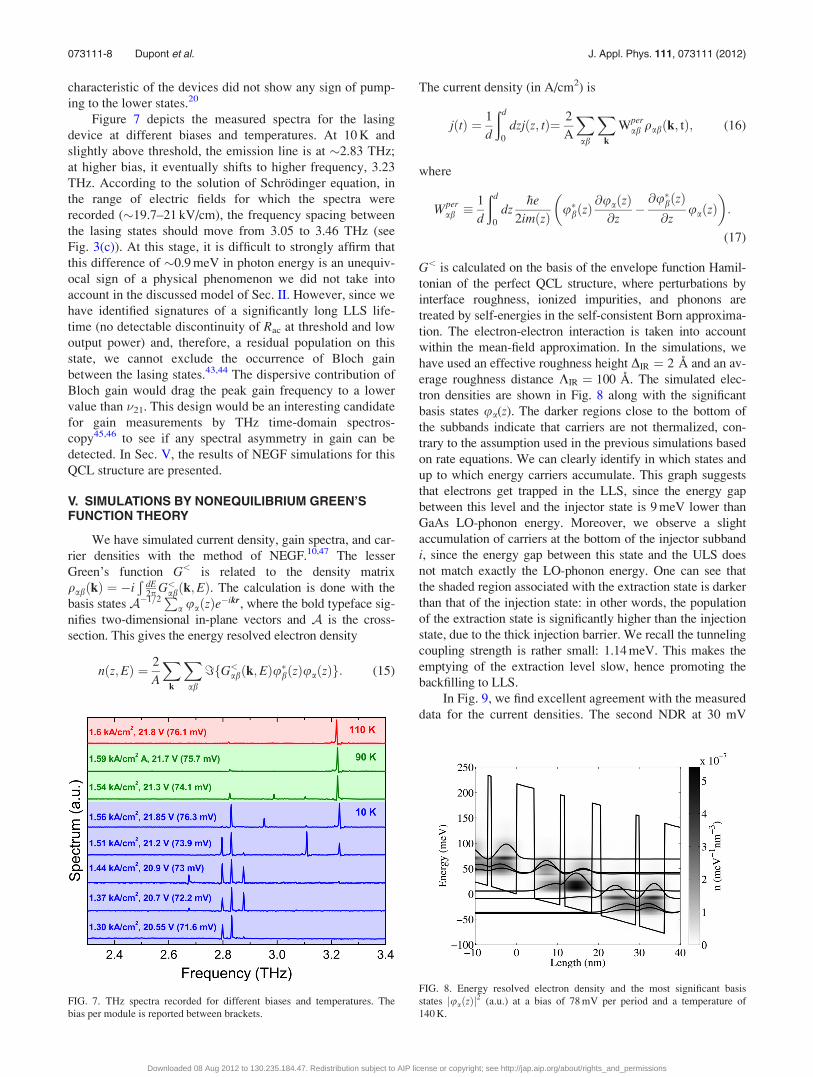
Figure 7 depicts the measured spectra for the lasing
device at different biases and temperatures. At 10 K and
slightly above threshold, the emission line is at �2.83 THz;
at higher bias, it eventually shifts to higher frequency, 3.23
THz. According to the solution of Schrodinger equation, in
the range of electric fields for which the spectra were
recorded (�19.7–21 kV/cm), the frequency spacing between
the lasing states should move from 3.05 to 3.46 THz (see
Fig. 3(c)). At this stage, it is difficult to strongly affirm that
this difference of �0.9 meV in photon energy is an unequiv-
ocal sign of a physical phenomenon we did not take into
account in the discussed model of Sec. II. However, since we
have identified signatures of a significantly long LLS life-
time (no detectable discontinuity of Rac at threshold and low
output power) and, therefore, a residual population on this
state, we cannot exclude the occurrence of Bloch gain
between the lasing states.43,44 The dispersive contribution of
Bloch gain would drag the peak gain frequency to a lower
value than �21. This design would be an interesting candidate
for gain measurements by THz time-domain spectros-
copy45,46 to see if any spectral asymmetry in gain can be
detected. In Sec. V, the results of NEGF simulations for this
QCL structure are presented.
V. SIMULATIONS BY NONEQUILIBRIUM GREEN’SFUNCTION THEORY
We have simulated current density, gain spectra, and car-
rier densities with the method of NEGF.10,47 The lesser
Green’s function G< is related to the density matrix
qabðkÞ ¼ �iÐ
dE2p G<
abðk;EÞ. The calculation is done with the
basis states A�1=2Pa uaðzÞe�ikr, where the bold typeface sig-
nifies two-dimensional in-plane vectors and A is the cross-
section. This gives the energy resolved electron density
nðz;EÞ ¼ 2
A
Xk
Xab
=fG<abðk;EÞu�bðzÞuaðzÞg: (15)
The current density (in A/cm2) is
jðtÞ ¼ 1
d
ðd
0
dzjðz; tÞ¼ 2
A
Xab
Xk
Wperab qabðk; tÞ; (16)
where
Wperab
1
d
ðd
0
dz�he
2imðzÞ u�bðzÞ@uaðzÞ@z
�@u�bðzÞ@z
uaðzÞ� �
:
(17)
G< is calculated on the basis of the envelope function Hamil-
tonian of the perfect QCL structure, where perturbations by
interface roughness, ionized impurities, and phonons are
treated by self-energies in the self-consistent Born approxima-
tion. The electron-electron interaction is taken into account
within the mean-field approximation. In the simulations, we
have used an effective roughness height DIR ¼ 2 A and an av-
erage roughness distance KIR ¼ 100 A. The simulated elec-
tron densities are shown in Fig. 8 along with the significant
basis states ua(z). The darker regions close to the bottom of
the subbands indicate that carriers are not thermalized, con-
trary to the assumption used in the previous simulations based
on rate equations. We can clearly identify in which states and
up to which energy carriers accumulate. This graph suggests
that electrons get trapped in the LLS, since the energy gap
between this level and the injector state is 9 meV lower than
GaAs LO-phonon energy. Moreover, we observe a slight
accumulation of carriers at the bottom of the injector subband
i, since the energy gap between this state and the ULS does
not match exactly the LO-phonon energy. One can see that
the shaded region associated with the extraction state is darker
than that of the injection state: in other words, the population
of the extraction state is significantly higher than the injection
state, due to the thick injection barrier. We recall the tunneling
coupling strength is rather small: 1.14 meV. This makes the
emptying of the extraction level slow, hence promoting the
backfilling to LLS.
In Fig. 9, we find excellent agreement with the measured
data for the current densities. The second NDR at 30 mV
FIG. 7. THz spectra recorded for different biases and temperatures. The
bias per module is reported between brackets.
FIG. 8. Energy resolved electron density and the most significant basis
states juaðzÞj2 (a.u.) at a bias of 78 mV per period and a temperature of
140 K.
073111-8 Dupont et al. J. Appl. Phys. 111, 073111 (2012)
Downloaded 08 Aug 2012 to 130.235.184.47. Redistribution subject to AIP license or copyright; see http://jap.aip.org/about/rights_and_permissions

predicted by NEGF simulations is confirmed by the experi-
ment. The device was driven in current mode, hence, on the
oscilloscope, the voltage suddenly changed from 30 mV to
60 mV. The first tunneling resonance is predicted at around
4.3 kV/cm, whereas the experimental current density shows
a shoulder at 4.8 kV/cm (see the vertical arrow in Fig. 9),
which was attributed to sequential tunneling across three
modules from en�1! 1 n! 2 nþ1 in Sec. IV. NEGF simula-
tions performed around the first resonance confirmed a non-
negligible transport channel by phonon emission (and more
marginally by other scattering sources) from the anticrossed
levels 2 and i. Experimentally, the current is more phonon
driven at the first resonance than predicted in NEGF simula-
tions. For this latter model, the scattering potentials are very
efficient when levels e and 1 are best aligned and, therefore,
give rise to a current peaked at 4.3 kV/cm. The current den-
sity simulated by the rate equation model (without the effect
of stimulated emission) is also displayed in Fig. 9, showing
the maximum current levels are comparable for both models.
Finally, gain spectra have been simulated using NEGF
at different temperatures and voltage biases. The results of
these simulations for a fixed bias of 21.5 kV/cm (78 mV per
module) and a temperature of 140 K are displayed in Fig. 10.
It is important to point out that simulations at low tempera-
tures showed a maximum gain and peak gain frequency
lower than expected from the measurements. There were nu-
merical problems at low temperature, due to the lack of e-e
scattering in the simulations, whereas, at 140 K, the acoustic
phonons assist to a higher degree in the thermalization of the
carriers. An underestimated thermalization of the carriers at
low temperature would enhance the trapping of electrons on
the LLS and subsequently result in a reduced population
inversion and a higher contribution from Bloch gain. At
140 K, a gain of 37 cm�1 at 3.4 THz is predicted, a value that
is consistent with previous measurements of waveguide loss
by cavity frequency pulling.48 Theoretically, from 72 to
76 mV per module, the peak gain frequency moves from 2.8
to 3.24 THz, while experimentally, the laser emission shifts
from 2.8 to 3.23 THz in a similar bias range (71.6 to
76.3 mV) at 10 K. This latter comparison would support the
hypothesis that the simulated thermalization at 140 K by
NEGF is close to the actual thermalization at lower tempera-
tures. At 76 mV per module, the gain bandwidth derived by
NEGF simulations is �1.38 THz, a value slightly larger than
the assumed value of 1 THz used in the simulations based on
rate equations.
VI. CONCLUSION
This paper presented a THz SA-QCL design with con-
secutive “phonon-photon-phonon” emissions. The simplicity
of the lasing scheme made it convenient to calculate the
energy level populations and lifetimes using a rate equation
model. The first iteration structure was designed by optimiz-
ing a figure of merit defined as the product of population
inversion and oscillator strength. The optimum design at
150 K only took LO-phonon scattering into account in trans-
port calculations and assumed a Maxwell-Boltzmann distri-
bution of carriers, with a temperature of 200 K in the
subbands. In the designed structure, the lasing states were
fairly isolated from higher bands and not perturbed by tun-
neling. The fabricated device using Au double metal wave-
guide lased up to 138 K. The voltage-current density
characteristic of the device showed no obvious discontinuity
in the differential resistance at threshold, an observation con-
sistent with the low output power of the laser. The rate equa-
tion model suggests that these two effects stem from rather
slow depopulation of the LLS, due to smaller-than-phonon-
energy E1e. This hypothesis was confirmed by NEGF calcu-
lations. Both rate equation and NEGF calculations indicated
FIG. 9. Current density vs voltage bias per period: experimental data (scat-
tered points) at 10 K in pulsed mode and comparison with simulations by
nonequilibrium Green’s function formalism. The position of the first reso-
nance at �4.8 kV/cm in the experimental data is highlighted by a vertical
arrow and is attributed to sequential tunneling from e to 1 and then 2 in three
consecutive periods. The NEGF simulation is performed for higher tempera-
tures than the experimental data, but the simulated results are weakly tem-
perature sensitive. Moreover, by the end of the current pulses (250 ns), it is
well known that the lattice temperature can be several tens of kelvin higher
than heat sink. The large fluctuations around 40–60 meV are artifacts of the
simulation. The device was driven in current mode, which explains why the
valley of the second NDR predicted by theory is not observed. The simu-
lated current density by the rate equation model is plotted in dashed line.
The dash-dot line represents the strong leakage current from the wrong
extraction channel 2-e.
FIG. 10. Gain spectra simulated using NEGF model at T¼ 140 K and differ-
ent biases per module.
073111-9 Dupont et al. J. Appl. Phys. 111, 073111 (2012)
Downloaded 08 Aug 2012 to 130.235.184.47. Redistribution subject to AIP license or copyright; see http://jap.aip.org/about/rights_and_permissions

that the tunneling barrier is the bottleneck of the carrier
transport and the carriers are piled up behind it.
Using the models discussed in this paper, we identified
the shortcomings of the first iteration design and addressed
them in detail for the next generations of THz SA-QCL
designs. We found out that it is important to maximize the
phonon scattering–assisted extraction and injection rates by a
better optimization of energy spacing between corresponding
subbands. Moreover, one has to take interface roughness scat-
tering into account in the optimization process. It was found
that interface roughness scattering, particularly between the
lasing states, is comparable to the LO-phonon scattering rates
and should not be neglected. Its effect on population dynamics
and linewidth of the lasing transition also has to be considered
for the next generation of THz SA-QCL designs.
The proposed lasing scheme in this work benefits from a
rather simple operation principle. Consequently, such a 4-
level quantum mechanical structure provides a unique plat-
form to study experimentally various debated effects in THz
QCLs, including effect of interface roughness on population
dynamics and gain linewidth. The authors suggest conducting
a comprehensive doping study to elucidate the debated topic
of free carrier absorption and the role of e-e and e-impurity
scatterings in THz QCL. Furthermore, one can explore the
effect of injection tunneling barrier thickness on the coherence
of the transport and its effect on the device performance. Fur-
ther understanding of the carrier dynamics and gain is possible
by microprobe photoluminescence experiments to study the
electron distributions in the different subbands and by THz
time-domain spectroscopy to investigate the possibility of
Bloch gain in such a structure, respectively.
ACKNOWLEDGMENTS
The authors would like to thank Dr. Marek Korkusinski
from NRC for providing the genetic algorithm. We acknowl-
edge Dr. Alpar Matyas and Dr. Christian Jirauschek from
Technische Universitat Munchen. We also would like to
acknowledge the supports from Natural Science and Engi-
neering Research Council (NSERC) of Canada, from Cana-
dian Foundation of Innovation (CFI), from the Ontario
Research Fund (ORF), and CMC Microsystems. H.C.L. was
supported in part by the National Major Basic Research
Project (2011CB925603) and the Shanghai Municipal Major
Basic Research Project (09DJ1400102).
1R. Kohler, A. Tredicucci, F. Beltram, H. E. Beere, E. H. Linfield, A. G.
Davies, D. Ritchie, R. C. Iotti, and F. Rossi, Nature 417, 156 (2002).2S. Fathololoumi, E. Dupont, C. Chan, Z. Wasilewski, S. Laframboise,
D. Ban, A. Matyas, C. Jirauschek, Q. Hu, and H. C. Liu, Opt. Express 20,
3866 (2012).3M. A. Belkin, J. A. Fan, S. Hormoz, F. Capasso, S. P. Khanna, M. Lachab,
A. G. Davies, and E. H. Linfield, Opt. Express 16, 3242 (2008).4S. Kumar, Q. Hu, and J. L. Reno, Appl. Phys. Lett. 94, 131105 (2009).5M. A. Belkin, Q. J. Wang, C. Pflugl, A. Belyanin, S. P. Khanna, A. G.
Davies, E. H. Linfield, and F. Capasso, IEEE J. Sel. Top. Quantum Elec-
tron. 15, 952 (2009).6M. Tonouchi, Nat. Photonics. 1, 97 (2007).7G. Scalari, R. Terazzi, M. Giovannini, N. Hoyler, and J. Faist, Appl. Phys.
Lett. 91, 032103 (2007).8S. Kumar and Q. Hu, Phys. Rev. B 80, 245316 (2009).9E. Dupont, S. Fathololoumi, and H. C. Liu, Phys. Rev. B 81, 205311 (2010).
10S. C. Lee and A. Wacker, Phys. Rev. B 66, 245314 (2002).11T. Kubis, C. Yeh, P. Vogl, A. Benz, G. Fasching, and C. Deutsch, Phys.
Rev. B 79, 195323 (2009).12T. Schmielau and M. Pereira, Appl. Phys. Lett. 95, 231111 (2009).13H. Callebaut, S. Kumar, B. S. Williams, Q. Hu, and J. L. Reno, Appl.
Phys. Lett. 83, 207 (2003).14C. Jirauschek and P. Lugli, J. Appl. Phys. 105, 123102 (2009).15C. Deutsch, A. Benz, H. Detz, P. Klang, M. Nobile, A. M. Andrews, W.
Schrenk, T. Kubis, P. Vogl, G. Strasser, and K. Unterrainer, Appl. Phys.
Lett. 97, 261110 (2010).16H. Yasuda, T. Kubis, P. Vogl, N. Sekine, I. Hosako, and K. Hirakawa,
Appl. Phys. Lett. 94, 151109 (2009).17T. Kubis, S. R. Mehrotra, and G. Klimeck, Appl. Phys. Lett. 97, 261106
(2010).18S. Kumar, C. W. I. Chan, Q. Hu, and J. L. Reno, Nat. Phys. 7, 166 (2011).19M. Yamanishi, K. Fujita, T. Edamura, and H. Kan, Opt. Express 16, 20748
(2008).20M. Yamanishi, K. Fujita, T. Kubis, N. Yu, T. Edamura, K. Tanaka, G. Kli-
meck, and F. Capasso, paper presented at Eleventh International Confer-
ence on Intersubband Transitions in Quantum Wells, Badesi, Italy, 11–17
September 2011.21R. Nelander and A. Wacker, Appl. Phys. Lett. 92, 081102 (2008).22A. Wacker, R. Nelander, and C. Weber, in Novel In-Plane Semi-Conductor
Lasers VIII, edited by A. A. Belyanin and P. M. Smowton (SPIE, Belling-
ham, WA, 2009), Vol. 7230, p. 72301A.23G. Scalari, M. I. Amanti, R. Terazzi, M. Beck, C. Walther, and J. Faist,
Opt. Express 7, 8043 (2010).24S. Fathololoumi, E. Dupont, Z. R. Wasilewski, S. R. Laframboise, D. Ban,
and H. C. Liu, paper presented at Eleventh International Conference on
Intersubband Transitions in Quantum Wells, Badesi, Italy, 11–17 Septem-
ber 2011.25K. Fujita, M. Yamanishi, T. Edamura, A. Sugiyama, and S. Furuta, Appl.
Phys. Lett. 97, 201109 (2010).26S. Kumar, C. W. I. Chan, Q. Hu, and J. L. Reno, Appl. Phys. Lett. 95,
141110 (2009).27T. Kubis and P. Vogl, J. Phys.: Conf. Ser. 193, 012063 (2009).28A. Wacker, Appl. Phys. Lett. 97, 081105 (2010).29J. B. Khurgin and Y. Dikmelik, Opt. Eng. 49, 111110 (2010).30F. Carosella, C. Ndebeka-Bandou, R. Ferreira, E. Dupont, K. Unterrainer,
S. Strasser, A. Wacker, and G. Bastard, Phys. Rev. B 85, 085310 (2012).31G. Scalari, C. Walther, L. Sirigu, M. L. Sadowski, H. Beere, D. Ritchie, N.
Hoyler, M. Giovannini, and J. Faist, Phys. Rev. B 76, 115305 (2007).32T. Unuma, T. Takahashi, T. Noda, M. Yoshita, H. Sakaki, M. Baba, and
H. Akiyama, Appl. Phys. Lett. 78, 3448 (2001).33S. Tsujino, A. Borak, E. Muller, M. Scheinert, C. V. Falub, H. Sigg, D. Grutz-
macher, M. Giovannini, and J. Faist, Appl. Phys. Lett. 86, 062113 (2005).34Z. Wasilewski, X. Wu, and E. Dupont, private communication (2010).35B. S. Williams, S. Kumar, H. Callebaut, Q. Hu, and J. L. Reno, Appl.
Phys. Lett. 83, 2124 (2003).36S. Fathololoumi, E. Dupont, S. Razavipour, S. R. Laframboise, G. Parent,
Z. Wasilewski, H. C. Liu, and D. Ban, Semicond. Sci. Technol. 26,
105021 (2011).37Discontinuities of Rac at threshold �15% were observed on another SA-
QCL with a lower lasing oscillator strength.38P. Harrison, Appl. Phys. Lett. 75, 2800 (1999).39O. Bonno, J.-L. Thobel, and F. Dessenne, J. Appl. Phys. 97, 043702 (2005).40M. S. Vitiello, G. Scarmacio, V. Spagnolo, T. Losco, R. P. Green, A. Tredi-
cucci, H. E. Beere, and D. A. Ritchie, Appl. Phys. Lett. 88, 241109 (2006).41Y. Chassagneux, Q. J. Wang, S. P. Khanna, E. Strupiechonski, J.-R.
Coudevylle, E. H. Linfield, A. G. Davies, F. Capasso, M. A. Belkin, and
R. Colombelli, IEEE Trans. Terahertz Sci. Technol. 2, 83 (2012).42S. Kumar, B. S. Williams, Q. Hu, and J. L. Reno, Appl. Phys. Lett. 88,
121123 (2006).43H. Willenberg, G. H. Dohler, and J. Faist, Phys. Rev. B 67, 085315 (2003).44R. Terazzi, T. Gresch, M. Giovannini, N. Hoyler, N. Sekine, and J. Faist,
Nat. Phys. 3, 329 (2007).45J. Kroll, J. Darmo, S. S. Dhillon, X. Marcadet, M. Calligaro, C. Sirtori,
and K. Unterrainer, Nature 449, 698 (2007).46D. Burghoff, T.-Y. Kao, D. Ban, A. W. M. Lee, Q. Hu, and J. Reno, Appl.
Phys. Lett. 98, 061112 (2011).47C.-S. Lee, F. Banit, M. Woerner, and A. Wacker, Phys. Rev. B 73, 245320
(2006).48L. A. Dunbar, R. Houdre, G. Scalari, L. Sirugu, M. Giovannini, and
J. Faist, Appl. Phys. Lett. 90, 141114 (2007).
073111-10 Dupont et al. J. Appl. Phys. 111, 073111 (2012)
Downloaded 08 Aug 2012 to 130.235.184.47. Redistribution subject to AIP license or copyright; see http://jap.aip.org/about/rights_and_permissions