a power-efficient noise canceling technique using …kobaweb/news/pdf/2013/vietnam-a_power... · a...
TRANSCRIPT

THE INSTITUTE OF ELECTRONICS, IEICE ICDV 2013
INFORMATION AND COMMUNICATION ENGINEERS
Copyright ©2013 by IEICE
A Power-Efficient Noise Canceling Technique Using Signal-Suppression Feed-forward for Wideband LNAs
Daiki Oki, Satoru Kawauchi, Li CongBing, Masataka Kamiyama (Gunma Univ.)
Seiichi Banba, Toru Dan, Nobuo Takahashi, Koji Sakata (Sanyo Semiconductor Co., Ltd.)
Haruo Kobayashi, Nobukazu Takai (Gunma Univ.)
Abstract This paper presents a power-efficient noise-canceling technique based on the feed-forward amplifiers,
considering a fundamental tradeoff between noise figure (NF) and power consumption in the design of wide-band amplifiers.
By suppressing the input signal of the noise cancellation amplifier, the nonlinear effect on the amplifier can be reduced, as well
as the power consumption can be smaller. Furthermore, as a lower gain of the noise-canceling sub-amplifier can be achieved
simultaneously, further reduction of the power consumption becomes possible. The verification of the proposed technique is
conducted with Spectre simulation using 90nm CMOS process.
Keyword Noise-canceling, Feed-forward, Low-noise amplifier (LNA), Wide band
1. Introduction
Wide-band amplifiers suffer from an essential tradeoff
between input impedance matching and noise figure (NF).
Generally, wide-band low-noise amplifier (LNA) achieves
a better noise figure when the value of gm increases.
However, by conducting common input impedance
matching, it is difficult to adjust gm to an expected value.
The corresponding solution is introduced in [1 ], which
consists of a main amplifier (M i and R f) for input
impedance matching as well as signal amplification and a
noise-canceling sub-amplifier for low noise figure (Fig. 1).
In this solution, channel thermal noise generated in
matching and signal amplification device M i is fed back by
resistance R f , and canceled by noise cancellation amplifier
Av,c. By means of this, the tradeoff between the input
impedance matching and the noise figure is broken, and a
wide-band LNA with low noise figure becomes possible.
Furthermore, the distortion generated in M i can be
canceled simultaneously in a similar way. Though having
these advantages, this solution has a drawback that the
power consumption of the noise-canceling amplifier Av,c
tends to be comparatively large.
In this paper, a signal-suppression technique, which
applies the signal-null technique [2][3] , is proposed to
suppress the power consumption of the noise-canceling
amplifier. By exploiting an inverting amplifier where the
output is the inverse of the input, the small-signal input of
the noise-canceling amplifier Av,c can be suppressed. And
for Av,c, the tradeoff between the power consumption and
the nonlinearity can be mitigated. Compared with the
existing solution, this proposal reduces the power
consumption of the noise-canceling amplifier, while
inherits the existing advantages such as breaking the
tradeoff between input impedance matching and noise
figure, canceling distortion.
Fig.1. Conventional noise-canceling LNA.
This paper is organized as follows. Section 2 reviews
the existing noise-canceling technique. Section 3
describes the detailed principle of the proposed technique.
Section 4 shows the simulation results. Finally, Section 5
provides conclusions.
2. Conventional Noise-Canceling Technique
In this section, the conventional wide-band LNA
noise-canceling technique is reviewed, which is illustrated
in Fig. 1. Low noise figure is achieved by canceling the
channel thermal noise generated in matching device M i.
The channel thermal noise travels in the direction y → R f
→ x → Rs to the ground (when considering only the
noise, vs=0). By circuit inspection, the noise voltage at
nodes x and y are given by
𝑣𝑛,𝑥,𝑀𝑖 = 𝑅𝑠𝑖𝑛,𝑀𝑖
𝑣𝑛,𝑦,𝑀𝑖 = (𝑅𝑠 + 𝑅𝑓)𝑖𝑛,𝑀𝑖 (1)

Noise cancellation is achieved by adding the voltage
vn,y,Mi at node y to the output of the inverting amplifier Av,c,
which is a scaled negative replica of the voltage vn,x,Mi at
node x. Output noise voltage vout,n,Mi is equal to
𝑣𝑜𝑢𝑡,𝑛,𝑀𝑖 = 𝑣𝑦,𝑛,𝑀𝑖 − 𝐴𝑣,𝑐𝑣𝑥,𝑛,𝑀𝑖
= (𝑅𝑓 + 𝑅𝑆 − 𝐴𝑣,𝑐𝑅𝑆)𝑖𝑛,𝑀𝑖
When vout ,n,Mi=0, the goal of output noise cancellation is
reached. In this case, the gain of the noise-canceling
amplifier is denoted as Av,c,cancel, which is equal to
𝐴𝑣,𝑐,𝑐𝑎𝑛𝑐𝑒𝑙 = 1 +𝑅𝑓
𝑅𝑆
The input impedance is Z in=1/gMi. Correspondingly, the
input impedance matching condition is gMi=1/Rs. So when
the input impedance matching condition and the noise
cancellation requirement are satisfied at the matching
device M i and the noise-canceling amplifier Av,c
respectively, low noise figure can be realized. Equation
(4) expresses the voltage gain, where the input impedance
is Z in=1/gMi and the noise-canceling amplifier gain is
Av,c,cancel .
Av =𝑣𝑜𝑢𝑡
𝑣𝑥= 1 − 𝑔𝑀𝑖𝑅𝑓 − 𝐴𝑣,𝑐,𝑐𝑎𝑛𝑐𝑒𝑙
= −𝑔𝑀𝑖𝑅𝑓 −𝑅𝑓
𝑅𝑆
= −2𝑅𝑓
𝑅𝑆
Furthermore, the distortion generated in M i could be
cancelled simultaneously with almost the same principle.
The drawback of this existing circuit is that its power
consumption tends to be comparatively large due to the
matching device M i and the noise-canceling amplifier Av,c.
3. Proposed Technique
The block diagram of the proposed circuit is illustrated
in Fig. 2. It consists of main amplifiers M i, R f 1, R f 2, as well
as noise-canceling amplifier Av,c, which provides noise
cancellation for M i. Node a, which is between the
feedback resistors R f1 and R f 2, is selected as the input
point for the noise-canceling amplifier Av,c.
By suppressing the small-signal input of Av,c, the
nonlinear components generated in the noise -canceling
amplifier can be reduced, and low power consumption
becomes possible. Following the channel noise current in
M i, it is easy to obtain the connection between the noise
voltage vn,a,Mi at node a and the noise voltage vn,x,Mi at
node x (i.e. the input noise voltage of the existing
noise-canceling circuit) is: vn,a,Mi > vn,x,Mi. Compared with
the existing circuit, the proposed one realizes a lower
power consumption by breaking the tradeoff between the
impedance matching and the noise figure, and
simultaneously providing low-gain characteristics to the
noise-canceling amplifier Av,c, as it always enlarges the
input noise voltage. The noise of R f 1 passes through Av,c
without amplification, which is the same as the
conventional circuit. However, the noise of R f2 is
amplified by Av,c, therefore the corresponding noise
cancellation condition is different from M i.
Fig.2. Proposed noise-canceling LNA.
Fig.3. Noise analysis model of the proposed
noise-canceling LNA.
(i) Noise Cancellation Principle
In Fig.3, the noise of M i, R f1 and R f 2 are modeled as
current sources. To understand the principle of noise
cancellation, the small-signal voltage and the noise
voltage at each node have been analyzed in detail.
Firstly, consider the noise voltage. Noise current in,Mi
travels from matching device to the ground by way of
feedback resisters R f 1, R f 2, Rs (the noise voltage of Vs is
equal to 0). Noise current in,Rf1 and in,Rf2 pass through
the feedback resisters Rf1 and Rf2 respectively, and
then circulate back.
The noise voltages vn,a,Mi and vn,y,Mi, which are
generated at node a and node y respectively, are given as
follows:
𝑣𝑛,𝑎,𝑀𝑖 = (𝑅𝑠 + 𝑅𝑓2)𝑖𝑛,𝑀𝑖 − 𝑅𝑓2𝑖𝑛,𝑅𝑓2
(2)
(3)
(4)
(5)
𝑣𝑛,𝑦,𝑀𝑖 = (𝑅𝑠 + 𝑅𝑓1 + 𝑅𝑓2)𝑖𝑛,𝑀𝑖 − 𝑅𝑓1𝑖𝑛,𝑅𝑓1 − 𝑅𝑓2𝑖𝑛,𝑅𝑓1
The output noise voltage vn,out is
𝑣𝑛,𝑜𝑢𝑡 = 𝑣𝑛,𝑦,𝑀𝑖 − 𝐴𝑣.𝑐𝑣𝑛,𝑎,𝑀𝑖
The equivalent output noise |vn,out|2 can be achieved
based on equations (5) and (6).
|𝑣𝑛,𝑜𝑢𝑡|2
= 4𝑘𝑇𝐵 {|𝑅𝑆 + 𝑅𝑓1 + 𝑅𝑓2 − 𝐴𝑣,𝑐|2
𝛾𝑔𝑀𝑖 + 𝑅𝑓1
+ |1 − 𝐴𝑣,𝑐|2
𝑅𝑓2}
𝛾 is the excess noise factor for the short-channel
device. When |vn,out|2 takes the minimum value,
the corresponding gain of the noise-canceling amplifier
Av,c is expressed as Av,cancel:
𝐴𝑣,𝑐𝑎𝑛𝑐𝑒𝑙 =(𝑅𝑆 + 𝑅𝑓1 + 𝑅𝑓2)(𝑅𝑆 + 𝑅𝑓2)𝛾𝑔𝑀𝑖 + 𝑅𝑓2
(𝑅𝑆 + 𝑅𝑓2)2
𝛾𝑔𝑀𝑖 + 𝑅𝑓2
The above equation is regarded as the noise
cancellation condition.
Secondly, consider the small-signal voltage. vy/vx
represents the transfer function from node x to node y, i.e.
the voltage gain of the main amplifier. And va/vx expresses
the transfer function from node x to node a.
𝐴𝑣,𝑐𝑜𝑟𝑒 =𝑣𝑦
𝑣𝑥= 1 − (𝑅𝑓1 + 𝑅𝑓2)𝑔𝑀𝑖
𝑣𝑎
𝑣𝑥= 1 − 𝑅𝑓2𝑔𝑀𝑖
vy and vx have opposite signs when R f 2gMi<1<(R f 1+R f 2)gMi.
In equation (3), the noise voltages at node a and node y
have the same sign, while the small -signal voltage has an
opposite one. This provides a possibility for noise
cancellation. When the noise cancellation condition Av,c
=Av,cancel is satisfied, the small-signal voltage gain Av
is equal to
𝐴𝑣 = 1 − (𝑅𝑓1 + 𝑅𝑓2)𝑔𝑚𝑖 − 𝐴𝑣,𝑐(1 − 𝑅𝑓2𝑔𝑀𝑖)
= 1 − (Rf1 + Rf2)gMi
−(𝑅𝑆 + 𝑅𝑓1 + 𝑅𝑓2)(𝑅𝑆 + 𝑅𝑓2)𝛾𝑔𝑀𝑖 + 𝑅𝑓2
(𝑅𝑆 + 𝑅𝑓2)2
𝛾𝑔𝑀𝑖 + 𝑅𝑓2
(1 − 𝑅𝑓2𝑔𝑀𝑖)
Thirdly, consider the input impedance matching. The
input impedance is Z in=1/gMi, and the corresponding input
impedance matching condition is Z in=1/gMi=Rs. According
to equation (4), Av,c affects the noise figurer, and gMi
influences the input impedance matching. By adjusting
these two parameters, the tradeoff between the noise
figure and the input impedance matching can be dissolved.
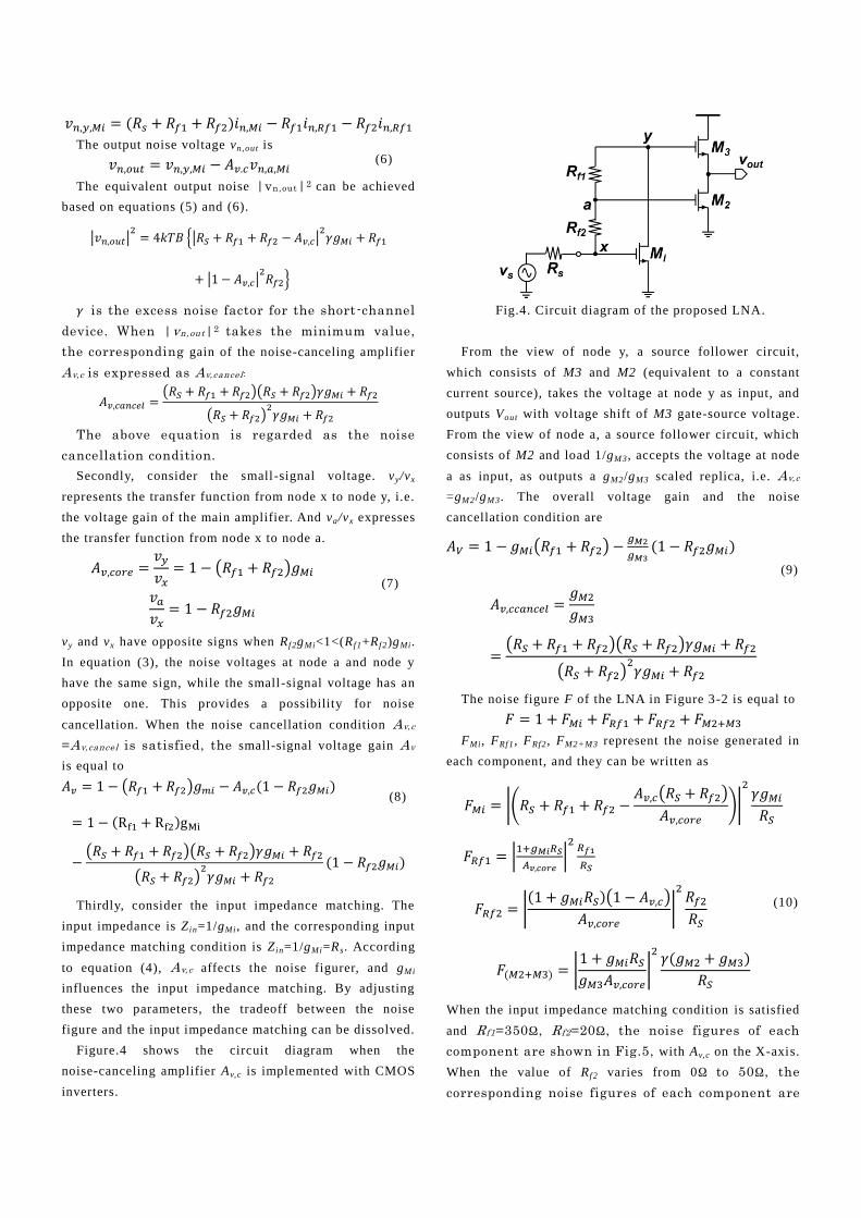
Figure.4 shows the circuit diagram when the
noise-canceling amplifier Av,c is implemented with CMOS
inverters.
Fig.4. Circuit diagram of the proposed LNA.
From the view of node y, a source follower circuit,
which consists of M3 and M2 (equivalent to a constant
current source), takes the voltage at node y as input, and
outputs Vout with voltage shift of M3 gate-source voltage.
From the view of node a, a source follower circuit, which
consists of M2 and load 1/gM3, accepts the voltage at node
a as input, as outputs a gM2/gM3 scaled replica, i.e. Av,c
=gM2/gM3. The overall voltage gain and the noise
cancellation condition are
𝐴𝑉 = 1 − 𝑔𝑀𝑖(𝑅𝑓1 + 𝑅𝑓2) −𝑔𝑀2
𝑔𝑀3(1 − 𝑅𝑓2𝑔𝑀𝑖)
𝐴𝑣,𝑐𝑐𝑎𝑛𝑐𝑒𝑙 =𝑔𝑀2
𝑔𝑀3
=(𝑅𝑆 + 𝑅𝑓1 + 𝑅𝑓2)(𝑅𝑆 + 𝑅𝑓2)𝛾𝑔𝑀𝑖 + 𝑅𝑓2
(𝑅𝑆 + 𝑅𝑓2)2
𝛾𝑔𝑀𝑖 + 𝑅𝑓2
The noise figure F of the LNA in Figure 3-2 is equal to
𝐹 = 1 + 𝐹𝑀𝑖 + 𝐹𝑅𝑓1 + 𝐹𝑅𝑓2 + 𝐹𝑀2+𝑀3
FMi, FRf1, FRf2, FM2+M3 represent the noise generated in
each component, and they can be written as
𝐹𝑀𝑖 = |(𝑅𝑆 + 𝑅𝑓1 + 𝑅𝑓2 −𝐴𝑣,𝑐(𝑅𝑆 + 𝑅𝑓2)
𝐴𝑣,𝑐𝑜𝑟𝑒)|
2𝛾𝑔𝑀𝑖
𝑅𝑆
𝐹𝑅𝑓1 = |1+𝑔𝑀𝑖𝑅𝑆
𝐴𝑣,𝑐𝑜𝑟𝑒|
2𝑅𝑓1
𝑅𝑆
𝐹𝑅𝑓2 = |(1 + 𝑔𝑀𝑖𝑅𝑆)(1 − 𝐴𝑣,𝑐)
𝐴𝑣,𝑐𝑜𝑟𝑒|
2𝑅𝑓2
𝑅𝑆
𝐹(𝑀2+𝑀3) = |1 + 𝑔𝑀𝑖𝑅𝑆
𝑔𝑀3𝐴𝑣,𝑐𝑜𝑟𝑒|
2𝛾(𝑔𝑀2 + 𝑔𝑀3)
𝑅𝑆
When the input impedance matching condition is satisfied
and Rf1=350Ω, Rf2=20Ω, the noise figures of each
component are shown in Fig.5, with Av,c on the X-axis.
When the value of R f 2 varies from 0Ω to 50Ω, the
corresponding noise figures of each component are
(7)
(8)
(9)
(10)
(6)

illustrated in Fig.6.
Fig.5. Noise figures of each component when Av,c varies
(R f1=350Ω, R f 2=20Ω)
Fig.6. Noise figures of each component when Av,c varies
(R f2 varies from 0Ω to 50Ω)
(ii) Distortion Cancellation
The distortion cancellation can be conducted on the
same principle of the noise cancellation. The remained
nonlinear component at node a is amplified by noise
canceller Av,c, and added to the one at node y.
The generated current in matching device M i can be
written as iMi=gmvgs+iNL, and correspondingly, the
voltages at node a and y are
𝑣𝑎 = 𝑣𝑆 − (𝑅𝑠 + 𝑅𝑓2)𝑖𝑛,𝑀𝑖(𝑔𝑀𝑖 + 𝐼𝑁𝐿)
𝑣𝑣𝑦 = 𝑣𝑆 − 𝐴𝑣,𝑐(𝑅𝑠 + 𝑅𝑓1 + 𝑅𝑓2)𝑖𝑛,𝑀𝑖(𝑔𝑀𝑖
+ 𝐼𝑁𝐿)
Equation (11) is similar to equation (3). The distortion
cancellation can be achieved under the same condition as
the noise cancellation
Av,c=Av,cancel=1+R f 1/(RS+R f2).
Through comparing equations (9) and (11), it is easy to
understand that the optimal points of the noise
cancellation and the distortion cancellation are not in
alignment with each other, as the noise takes M i, R f 1, and
R f 2 into consideration, while the distortion takes only M i
into account. So it is necessary to take both the
performance of noise and the performance of distortion
into design consideration.
(iii) Signal-Suppression Technique
In general, there exists a tradeoff between the MOS
power consumption and the linearity. The connections
between MOS drain current ID and transistor gm can be
written as
𝑔𝑚 =2𝐼𝐷
𝑉𝐺𝑆−𝑉𝑇𝐻
This equation shows that when gm is constant, the lower
the VGS is, the smaller the drain current ID will be.
However, in terms of MOS, the lower the VGS is, the larger
the nonlinear effect will be. That is to say, there exists a
tradeoff between the current consumption ID (i.e. the
power consumption) and the linearity.
The so-called signal-suppression technique is used to
alleviate this tradeoff. By suppressing the small-signal
input, the tradeoff between MOS power consumption and
linearity can be mitigated.
In the proposed circuit, the small-signal voltage of node
a can be changed to a lower value than that of node x (i.e.
the input voltage of noise-cancelling amplifier Av,c in the
existing circuit) by adjusting the value of R f2.
Correspondingly, the power consumption of M2 can be
reduced.
The small-signal voltage at node a can be written as
𝑣𝑎 = (1 − 𝑅𝑓2𝑔𝑀𝑖)𝑣𝑥
According to equation (13), when 0<Rf2gMi<2, |va|<
|vx|. This is regarded as the signal-suppression
condition.
The power consumption of the noise canceller is decided
by the drain current of M2. Signal-suppression technique
reduces the amplitude of the input signal of M2, therefore
decreases Vg-V t of M2. According to equation (12), the
drain current of M2 decreases correspondingly, which
leads to a low power consumption of the noise -canceling
amplifier Av,c.
4. Simulation
The proposed circuit is verified by Spectre simulation
with 90nm CMOS process. Simulation circuit diagram is
illustrated in Fig. 5.
Ideal components (Analog lib) are applied for resistor
(11)
(12)
(13)

and capacitor modeling, and real components (tsmc 90)
are used for MOS modeling. Inverter M ia and M ib
constitute the matching device. C2, RB2, VB2, C3, RB3, and
VB3 constitute the bias circuit for M2 and M3. irs is set as
an ideal current source in order to achieve a stable gm of
M2.
Fig.7. Simulation circuit diagram
Simulation result “Av,c vs. noise figure” is illustrated in
Fig.7, where the frequency of the input signal is 1GHz and
the value of R f2 varies from 0Ω to 50Ω. R f 1+R f 2 is a
constant value. The result shows that the noise of R f2 gives
a great impact on the circuit’s whole noise figure.
Fig.7. “Av,c vs. NF” when R f2 varies from 0Ω to 50Ω
When the value of Av,c satisfies the noise cancellation
condition under different R f2 values, the corresponding
“power consumption and NF” characteristics are
illustrated in Fig.8.
Fig.8. “Power consumption and NF” when R f2 varies
When R f1=350Ω, R f 2=20Ω, as well as the noise
cancellation condition and the distortion condition are
satisfied separately, the corresponding power consumption
and frequency characteristics are compared. When
R f 2=20Ω, the noise cancellation condition is Av,c=6, and
the distortion condition is Av,c=4.83. When these two
conditions are satisfied separately, the corresponding
power consumption is 8.23mW and 9.88mW. And when
these two conditions are satisfied simultaneously, e.g.
Av,c=5.42, the frequency characteristics are illustrated in
Fig.9.
(a)S11
0
1
2
3
4
5
6
7
8
9
10
1 2 3 4 5 6 7 8 9 10
NF
[dB
]
Av.c
Rf2=0Ω
Rf2=10Ω
Rf2=20Ω
Rf2=30Ω
Rf2=40Ω
Rf2=50Ω
0
1
2
3
4
5
6
0
2
4
6
8
10
12
14
16
0 10 20 30 40 50
NF
[dB
]
Pow
er[
mW
]
Rf2[Ω]
Power
NF
-20
-18
-16
-14
-12
-10
-8
-6
-4
-2
0
0 1 2 3 4 5 6
S1
1[d
B]
frequency[GHz]
Av.c=6
Av.c=5.42
Av.c=4.83

(b)S21
(c)NF
Fig.9. Comparison of frequency characteristics.
The two tones at 849 and 851MHz are used as input
signal frequency, and the power of the third -order
intermodulation distortion (IMD3) at 847MHz are
observed at the output in the simulation. The input
third-order intercept point (IIP3) is -1.99dBm under noise
cancellation condition, and -1.53dBm under distortion
cancellation condition.
Table.1 shows the results when R f 1=350Ω, R f 2=50Ω, as
well as Av,c satisfies the noise cancellation condition and
the distortion cancellation condition separately or
simultaneously.
Table.1. Simulation results when R f2=20Ω
5. Conclusion
In order to mitigate the tradeoff between the noise
figure and the power consumption in wide-band LNA
design, a novel scheme is proposed. This scheme employs
the noise-cancelling technique, which is based on
feed-forward amplifier, and the signal-suppression
technique, which is capable of reducing the power
consumption of the noise-cancelling amplifier.
In case of the noise-canceling amplifier Av,c, the
simulation results shows that there is almost no tradeoff
between the noise figure and the linearity. However, a
compromise exists between the NF and the power
consumption, which provides a lot of flexibility in the
design of wide-band LNA.
REFERENCES
[1] F. Bruccoleri, E. A. M. Klumperink, B. Nauta,
“Wide-Band CMOS Low-Noise Amplifier Exploiting
Thermal Noise Canceling,” IEEE Journal of Solid-State
Circuits, vol.39, no.2, pp.275-282 (Feb. 2004).
[2] C.-F. Li, S.-C. Chou, G.-H. Ke, P.-C. Huang,“ A
Power-Efficient Noise Suppression Technique Using
Signal-Nulled Feedback for Low-Noise Wideband
Amplifiers,” IEEE Trans on Circuits and Systems II :
Express Brief, vol.59, no.1, pp.1-5 (Jan. 2012).
[3] C.-F. Li, S.-C. Chou, P.-C. Huang, “A
Noise-Suppressed Amplifier with a Signal-Nulled
Feedback for Wideband Applications”, IEEE Asian
Solid-State Circuits Conference, Fukuoka, Japan (Nov.
2008).
0
2
4
6
8
10
12
14
16
18
0 1 2 3 4 5 6
S2
1[d
B]
frequency[GHz]
Av.c=6
Av.c=5.42
Av.c=4.83
0
0.5
1
1.5
2
2.5
3
3.5
4
4.5
5
0 1 2 3 4 5 6
NF
[dB
]
frequency[GHz]
Av.c=6
Av.c=5.42
Av.c=4.83
Av.c 4.83 5.42 6.00
Bandwidth 100-4600
MHz
100-4500
MHz
100-4000
MHz
S11(1GHz) -17.22dB -16.99dB -16.72dB
S21(1GHz) 14.96dB 15.08dB 15.17dB
NF(1GHz) 3.25dB 3.298dB 3.36dB
IIP3(847MHz) -1.99dBm -1.58dBm -1.53dBm
Power
Consumption
8.23mW 9.05mW 9.87mW