a roadmap to implementing metal -organic frameworks in
TRANSCRIPT

1
A Roadmap to Implementing Metal-Organic Frameworks in Electronic Devices: Challenges
and Critical Directions
Mark D. Allendorf, Adam Schwartzberg, Vitalie Stavila Sandia National Laboratories, 7011 East Ave., Livermore, CA 94550
A. Alec Talin Center for Nanoscale Science and Technology,
National Institute of Standards and Technology 100 Bureau Dr., Gaithersburg, MD 20899
Abstract: Metal-organic frameworks (MOFs) and related material classes are attracting considerable attention for applications such as gas storage, separations, and catalysis. In contrast, research focused on potential uses in electronic devices is in its infancy. Several sensing concepts in which the tailorable chemistry of MOFs is used to enhance sensitivity or provide chemical specificity have been demonstrated, but in only a few cases are MOFs an integral part of an actual device. The synthesis of a few electrically conducting MOFs and their well-known structural flexibility suggest that MOF-based electronic devices exploiting these properties could be constructed. It is clear, however, that new fabrication methods are required to take advantage of the unique properties of MOFs and extend their use to the realms of electronic circuitry. In this Concepts article, we describe the basic functional elements needed to fabricate electronic devices and summarize the current state of relevant MOF research, and then review recent work in which MOFs serve as active components in electronic devices. Finally, we propose a high-level roadmap for device-related MOF research, the objective of which is to stimulate thinking within the MOF community concerning the development these materials for applications including sensing, photonics, and microelectronics.
Introduction
The continuous decrease in the active dimensions of electronic devices, extending to the point of molecular-scale device functionality, creates the need for new fabrication approaches that can produce defect-free nanostructures. Techniques having single-digit nanometer resolution represent something of a “holy grail” in this field, but are extremely challenging to achieve. Although it is now possible to produce an amazing array of nanoscale materials and morphologies, assembling these into ordered arrays and integration with other materials remains a key challenge. Nevertheless, considerable progress is being made. Top-down methods, such as nanoimprint lithography (NIL), can already significantly exceed state-of-the-art photolithography[1] (193 nm as of 2009) and are now incorporated into the International Roadmap for Semiconductors[2] for sub-20 nm patterning. Bottom-up methods, on the other hand, offer a high degree of control over

2
both material properties and architecture. [3] Nanoporous templates are a promising avenue and can be used to direct synthesis of nanowires and nanoparticles.[4] However, it is difficult to create ordered pore arrays with dimensions below 10 nm; furthermore, the available pore spatial arrangements are limited to close-packed or in some cases square patterns. Hard templates, such as anodized aluminum oxide,[4e] mesoporous silica,[4d] and diblock copolymers,[4f] have rigid, well-defined pores, but are only attractive for device fabrication if they remain an integral part of the structure, because they are difficult to remove. Furthermore, it is generally not possible to tailor their intrinsic electrical properties. Alternatively, soft templates such as inverse micelles,[4c] typically have well-defined structures that persist only in solution. Consequently, there remains a need for simple fabrication methods that can create two- and three-dimensional ordered structures and which are adaptable to a wide variety of materials.
The advent of nanoporous supramolecular solids known as metal-organic frameworks (MOFs) suggests new ways to address these issues. The past decade experienced an explosion of new materials in this category and is spawning intense research across a wide spectrum of potential applications. MOFs are hybrid materials having both an inorganic and an organic component; their structure is comprised of metal ions or clusters that are connected by electron-donating “linker” groups to create a networked structure with rigid pores. Interest in using these materials in fields such as gas storage,[5] separations,[6] sensing,[7] and catalysis[8] is rapidly accelerating. In addition to MOFs, related categories of materials are also appearing, most notably covalent organic frameworks (COFs),[9] which are a main-group analogue to MOFs in which all bonding is covalent, and zeolite imidazolate frameworks (ZIFs),[10] which possess the topology of zeolites, but are composed of synthetically versatile imidazolate groups linked by coordination bonds to Zn(II) ions. The advantages of MOFs for the aforementioned applications are compelling and, as a result of the rational design possibilities inherent in these materials, both superior properties and new understanding with respect to the interaction of small molecules with nanoporous materials are being achieved.
With respect to the fabrication of ordered nanoscale structures, MOFs have several advantages. First, since they are themselves a highly ordered self-assembled nanostructure as a result of their crystallinity, their pore dimensions are completely defined, making knowledge of atomic positions possible. Second, the nanoporosity of their structure results from geometric factors associated with the bonding between their inorganic and organic components, enabling rational template design.[11] Third, unlike the template materials listed above, MOFs possess a high degree of synthetic flexibility with potentially widely tunable electrical, optical, and mechanical properties. For example, although most MOFs are dielectrics, only a few semiconducting frameworks are known[12] and theoretical predictions suggest others are possible.[13] MOFs that are magnetic,[14] ferroelectric,[15] proton-conducting,[16] and luminescent[7] are also known. Finally, their porosity creates the potential to introduce non-native functionality to a given structure by infusing the accessible volume with a second molecule or material. Moreover, because the chemical environment within the pore can be modified, it is possible to tailor the interface between the MOF and a templated material to stabilize specific materials or nanostructures. Consequently, MOFs and the broader category of

3
crystalline nanoporous frameworks (CNF) possess many of the properties of an ideal template.
The purpose of this article is to identify focus points for research needed to realize the concept of MOF-based device fabrication and review progress to date in both our laboratories and others. We first address the basic functions that a MOF could perform within a device and summarize the current state of MOF research relevant to these. We then review the field with respect to using MOFs as active components in devices (sensors in most cases). Finally, we propose a high-level roadmap, the objective of which is to stimulate thinking within the wider scientific community concerning the development and implementation of MOFs for electronic devices. It will be evident that expertise outside the field of supramolecular chemistry is required to address the issues highlighted by this roadmap, which we hope will lead to productive collaborative research among material scientists, physicists, and researchers from other branches of chemistry.
MOF functions within electronic devices
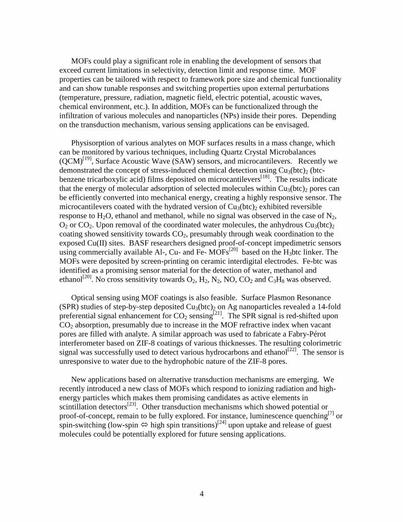
There are nearly endless possibilities for how MOFs could be used for device applications. However, electronic devices, be they semiconductor microelectronics, sensors, light-emitting or light absorbing, employ materials in a few basic ways. When considering MOFs as components of such devices, it is therefore necessary to understand how these materials function within the device and how they will interface with, or perhaps replace, other functional and structural elements. In this section we will discuss four critical applications and the advances that must be made for their realization. These applications, shown in Figure 1, are non-electronic, electronic (passive), electronic (active), and scaffolding.
Sensors. Figure 1a schematically represents the non-electronic MOF based device, in this case as a microelectromechanical system (MEMS) sensing modality. Here, the porous nature and tunable MOF chemistry provide selectivity and sensitivity to enable detection of a particular analyte or, potentially, to monitor a physical property such as temperature or pressure. In the case of molecular binding, the effect on the MOF could be, for example, a structural swelling as the MOF adsorbs or chemisorbs, a property of many MOFs that can occur with a magnitude much greater than found in, for example, fully inorganic nanoporous materials.[17] As a stand-alone material, this property is interesting, but not entirely useful. By attaching a MOF thin film to a microcantilever, however, it becomes a powerful sensing device. As shown in Figure 1a, the signal transduction mechanism could be the deflection of a laser that is focused onto a position-sensitive photodiode: as analyte binds to the MOF coating, the film swells, deflecting the cantilever, with the degree of displacement proportional to the amount of analyte bound. Alternatively, the strain induced at the MOF-sensor interface can be detected using a piezoresistor; this concept has already been demonstrated (see below).[18] Currently, this application is limited only by the development of MOFs with high chemical selectivity and the ability to grow these onto the desired substrate. One can imagine applying this technology to sensor arrays, making simultaneous detection of multiple analytes possible.
4
MOFs could play a significant role in enabling the development of sensors that
exceed current limitations in selectivity, detection limit and response time. MOF properties can be tailored with respect to framework pore size and chemical functionality and can show tunable responses and switching properties upon external perturbations (temperature, pressure, radiation, magnetic field, electric potential, acoustic waves, chemical environment, etc.). In addition, MOFs can be functionalized through the infiltration of various molecules and nanoparticles (NPs) inside their pores. Depending on the transduction mechanism, various sensing applications can be envisaged.
Physisorption of various analytes on MOF surfaces results in a mass change, which can be monitored by various techniques, including Quartz Crystal Microbalances (QCM)[19], Surface Acoustic Wave (SAW) sensors, and microcantilevers. Recently we demonstrated the concept of stress-induced chemical detection using Cu3(btc)2 (btc-benzene tricarboxylic acid) films deposited on microcantilevers[18]. The results indicate that the energy of molecular adsorption of selected molecules within Cu3(btc)2 pores can be efficiently converted into mechanical energy, creating a highly responsive sensor. The microcantilevers coated with the hydrated version of Cu3(btc)2 exhibited reversible response to H2O, ethanol and methanol, while no signal was observed in the case of N2, O2 or CO2. Upon removal of the coordinated water molecules, the anhydrous Cu3(btc)2 coating showed sensitivity towards CO2, presumably through weak coordination to the exposed Cu(II) sites. BASF researchers designed proof-of-concept impedimetric sensors using commercially available Al-, Cu- and Fe- MOFs[20] based on the H3btc linker. The MOFs were deposited by screen-printing on ceramic interdigital electrodes. Fe-btc was identified as a promising sensor material for the detection of water, methanol and ethanol[20]. No cross sensitivity towards O2, H2, N2, NO, CO2 and C3H8 was observed.
Optical sensing using MOF coatings is also feasible. Surface Plasmon Resonance (SPR) studies of step-by-step deposited Cu3(btc)2 on Ag nanoparticles revealed a 14-fold preferential signal enhancement for CO2 sensing[21]. The SPR signal is red-shifted upon CO2 absorption, presumably due to increase in the MOF refractive index when vacant pores are filled with analyte. A similar approach was used to fabricate a Fabry-Pérot interferometer based on ZIF-8 coatings of various thicknesses. The resulting colorimetric signal was successfully used to detect various hydrocarbons and ethanol[22]. The sensor is unresponsive to water due to the hydrophobic nature of the ZIF-8 pores.
New applications based on alternative transduction mechanisms are emerging. We recently introduced a new class of MOFs which respond to ionizing radiation and high-energy particles which makes them promising candidates as active elements in scintillation detectors[23]. Other transduction mechanisms which showed potential or proof-of-concept, remain to be fully explored. For instance, luminescence quenching[7] or spin-switching (low-spin high spin transitions)[24] upon uptake and release of guest molecules could be potentially explored for future sensing applications.
5
Figure 1. Potential functions of MOFs within electronic and microelectromechanical systems (MEMS).
Electronic-passive. In this case, the MOF simply functions as an electronic component that does not play a role in current transport or control, but is integral to device performance. The best example of this is low-k dielectrics, shown schematically in a transistor in Figure 1b. A major technological hurdle in the continued reduction of transistor size and electronic interconnects in processors is the development of low-k materials. As components become smaller and closer together, electronic “cross-talk” becomes a major issue, placing a serious limitation on how densely devices can be packed. Empirically, it is found that the development of faster processors scales directly with the development of new, low-k dielectrics. State-of-the-art dielectrics have k of ≈2.2 and incorporate air bubbles to improve their performance. Because MOFs are so porous, they contain significantly more air and should therefore have a significantly lower dielectric constant than any current low-k material.
Electronic-active. Here, the MOF plays an active role to pass or control current in some way. An example of this would be a p-n junction-based photovoltaic, as shown schematically in Figure 1c. In this example the MOF itself must be semi-conducting, with the potential for doping or Fermi-level control, and be tailored to absorb the solar spectrum and transfer the resulting excitons to the interface. There are many hurdles to overcome before this concept could be realized, including synthesis of semi-conducting MOFs (in its infancy);[12b, 25] crystalline MOF thin films have not been realized over large areas; and even applying contact electrodes to such porous materials is not well understood. However, there are reasons to continue development of MOF materials towards this goal. MOF based photovoltaics could be made to optimally absorb the solar spectrum by introducing a range of appropriate sensitizing molecules, they could be made extremely thin, flexible, and light due to the porosity and structural stability of MOFs, and they will likely be solution processable, which substantially decreases cost of production, a major factor in the low rate of usage and availability of photovoltaics.
MOF scaffolds. In this application, the MOF serves as a structural component in the device architecture. From a fabrication point of view, this could be the most difficult of the four MOF functions to implement. We have shown that silver nanowires can be

6
grown within MOF crystals using electron-beam reduction of silver salts.[26] Building on this result, we propose that nanowire growth could be controlled to produce electrical interconnects, as shown schematically in Figure 1d. The greatest issue currently with applying the amazing advances of nanowire synthesis to real-world applications is the difficulty of arranging and orienting them to create functioning structures. Because MOFs are inherently ordered, they could provide scaffolding along which nanowires could grow with both their orientation and spacing tightly controlled. This would allow for the development of single-digit nanometer-scale arrays of nanowires for any number of possible applications. There are several barriers that must be overcome before this concept can be realized. First, controlling the direction of nanowire growth and position is complex; however, the development of MOF heterostructures with controlled pore size and direction through a crystal will aid in this regard. Second, contacts between nanowires and the outside world must be made. A MOF crystal with thousands or ordered wires crossing each other at fixed intervals must still be connected at their terminus in order to make a functional device, and these connections would currently need to be produced manually via nanofabrication. With increased control it may be possible to use nano-imprint lithograph to make such connections. Ultimately, the potential of this device would be arrays of single nanometer transistors. The appeal of such a technology to computation is clear. In the following section, we assess the state of development with respect to these basic functions that a MOF might fulfill, which will set the stage for a roadmap to much more advanced uses of MOFs as device components.
Starting point for device fabrication: thin films
One of the first steps in systematic fabrication of MOF-based devices involves deposition of a MOF film or coating on a substrate. Stringent requirements for device performance require controlled deposition of films of desired morphology that are dense, homogenous and robust. For optical and magnetic devices, membranes, and sensors there are additional requirements to the thickness, crystallinity, as well as orientation of the film, which governs the pore structure of the deposited material. The deposition of MOF thin films can be achieved in situ, ex situ or by seeding methods. In-situ methods rely on substrate functionalization to allow preferential nucleation of MOF molecules and subsequent film growth[27] while ex-situ[28] and seeding methods[29] are based on direct deposition of previously synthesized MOF crystals on surfaces. Seeding is typically followed by a secondary growth step. Many materials can be used as substrates, including oxides, graphite, gold, copper, and other metals. However, to detect the secondary building units (SBUs) and to achieve some control over the orientation of the crystal growth, an appropriate functionalization of the substrate, with self-assembled monolayers (SAMs), for example, may be necessary[30].
Ex-situ synthesis. Ex-situ approaches to MOF film growth are typically based on the auto-assembly of preformed objects, typically nanocrystals and colloids[31]. In such a procedure, the first step consists in obtaining stable colloidal solutions by a careful choice of metal precursor, concentration, temperature and reaction duration[28]. Control of the thickness can be achieved through repetitive depositions followed by washing and drying. The main advantage of this route is the control over particle size, morphology,
7
crystallinity and porosity. In addition, the packing of the particles gives rise to inter-grain boundaries, and thus mesoscopic porosity. However, colloids of the appropriate size are needed; their synthesis often involves specialized synthetic techniques, such as microwave heating, ultrasonic synthesis or microemulssion methods. Moreover, the as-synthesized nanocrystals should assemble in a homogeneous and dense fashion. These conditions require a careful adjustment of synthesis conditions, including solvent, temperature, or the presence of additional linkers which act as stabilizers[27b] or coordination modulators[32]. Nevertheless, MOF nanocrystals have already been described for a number of structures. No preferred orientation has been obtained, but the use of anisotropic colloids instead of round-shaped particles may enable some progress in this direction[32].
Seeding methods. Seeding is proving extremely useful for the fabrication of selective gas membranes. Thus, membranes of ZIF-7 and ZIF-8 prepared by secondary seeded growth on porous α-alumina substrates showed high H2/N2, H2/CH4 and H2/CO2 gas separation factors.[29c-f] The typical procedure involves (i) synthesis of the initial MOF nanocrystals, (ii) deposition of the nanoparticles (NPs) on substrates and (iii) solvothermal growth of the film from the initial reagents. In addition to ZIFs, seeded growth was achieved by spin coating of nanocrystals of Cu3(btc)2
[29a], as well as by microwave-induced thermal deposition of MOF-5[29b], each followed by a secondary solvothermal growth step. Although widely used for membrane fabrication, the integration of films prepared by seeding techniques into devices seems difficult, since no masking or patterning techniques have been developed yet for such growth conditions.
Recently Makiura et al.[33],[34] introduced a variation of the seeding technique based on self-assembly of Langmuir-Blodgett films into 2D MOF multi-layers. The 2D sheets consist of cobalt-containing porphyrines linked together by copper ions. Individual sheets are prepared in a Langmuir-Blodgett apparatus and transferred onto the substrate. The layers interact by π - π stacking interactions between the pyridine groups, forming a perfectly oriented crystalline structure. The obtained supramolecular structure is called NAFS-1 and it only exists as a film. Obviously, this method is limited to layered- MOFs and no chemical bonds are created between the layers or between the MOF and the substrate, likely decreasing the stability of the structure.
In-situ growth. These techniques are more suitable for integrating MOF films with pre-existing devices that require tightly controlled patterned growth on the surface plane. The concept of selective anchoring of a MOF on a surface was first demonstrated for MOF-5 using a patterned COOH/CF3-terminated SAM[27a]. MOF-5 cannot grow on CF3-terminated SAM, but only on COOH-groups, allowing the formation of a 500 nm-thick non oriented film made of 100 nm sized cubic crystallites after 24 h. The concentrated synthesis solution has to be pre-treated solvothermally to initiate the formation of the SBUs; the deposition of the film is then continued at room temperature upon slow crystallization conditions. Subsequent studies showed that selective nucleation of MOF-5 can also occur on carboxylic acid terminated SAMs on SiO2 and ultrathin, amorphous Al2O3 adhesion layers[27b]. In the case of Cu3(btc)2, the film grows from very diluted solutions, however, up to 100 h are required to obtain a continuous film.[27c] Interestingly,

8
a highly oriented crystal growth takes place: {100} direction on COOH-terminated SAMs and {111} on OH-terminated SAMs. It was suggested that different molecular functionalities of the SAMs induce selective interactions of the growth species with the binding groups (OH or COOH), then grow into oriented crystals (vide infra). Similar growth conditions also proved successful for MIL-88B (Fe) film deposition on Au SAMs[27d]. However, in general, the films generated by solvothermal techniques display poor morphology[27a],[27b] and control over orientation and thickness[27c],[35],[36]. Schoedel et al. achieved better control over morphology and film orientation using a gel-layer approach, which effectively reduces the concentration of the reagents at the solution-substrate inter-phase during the solvothermal step[37]. Thus, high quality films of MIL-88B and its amine-derivative MIL-88B-NH2 were deposited on COOH- and OH-terminated SAMs using solutions of the metal salt and the appropriate linker in the presence of a poly(ethyleneglycol) gel.
In selected cases the growth of the MOF film from the mother solution takes place at room temperature[30]. Typically, a solution containing the MOF precursors is heated so as to induce the formation of the appropriate SBU and beginning of crystallization. After filtration and cooling down to room temperature, the substrates are immersed in the solution. Such a method was successfully applied for MOF-5[27a], Cu3(btc)2
[27c] MIL-88B[27d], as well as for various ZIFs[38],[39]. Repeated immersion steps in freshly prepared mother solutions enable the attachment of seeds and their further growth[22, 27j]. In the case of [Cu2(pzdc)2(pyz)]n (CPL-1; pzdc = pyrazine-2,3-dicarboxylate; pyz = pyrazine)[27j], the crystals tend to form plate-like crystals with preferred orientation in the {010} direction. Lu and Hupp deposited ZIF-8 on Si substrates and controlled the thickness of the film by the number of deposition cycles. No preferred orientation was found in this case, but a very precise control of film thickness is achieved (100 nm per cycle)[22]. In situ growth of MOF thin films from appropriately prepared mother solutions is a versatile technique; however such processes are very time consuming (up to several weeks) and a very good knowledge of the specific MOF system.
In contrast to established protocols of MOF thin film deposition using metal salts and the appropriate linker, electrochemical and redox approaches are based on in situ generation of the metal ions. This can be achieved either by anodic dissolution of a metal electrode or by galvanic displacement with a more noble metal. Crystalline films of Cu3(btc)2 have been prepared electrochemically[27k] or by galvanic displacement[27l]. The structural metal ion (Cu2+) is supplied either by anodic oxidation of the metallic substrate (Cu) or by galvanic displacement of copper with a more noble metal (e.g. Ag), then reacts with the organic linker. These electrochemical techniques offer close control over the film thickness and morphology and typically require short growth times; however they do not allow any control over the orientation of the crystals. In some cases, the metal ion can be generated in situ by oxidizing a metal surface. Thus, H2O2-treated Zn slices were shown to react with H3BTC under solvothermal conditions to generate compact Zn3(BTC)2 coatings [36]. Both electrochemical and redox approaches may serve as useful techniques to deposit patterned films on devices.

9
Figure 2. Schematic representation of the layer-by-layer growth of MOF thin films, illustrated for the growth of a pillar-type MOF (MOF-508 shown here). a) The substrate is initially functionalized with groups that bind the metal ions in the MOF; b) exposure to metal ions, followed by exposure to the first of two linkers (here shown as terephthalic acid), creates a two-dimensional layer; c) exposure to the second linker (here shown as bipyridine) creates the pillar structure; d) repeated metal ion-linker 1-linker 2 cycles builds up a layer-by-layer structure; e) nucleation requires some adjustment of the surface functional groups since the MOF unit cell and the spacing between the groups typically will not match.
A very promising approach to MOF film deposition is the layer-by-layer growth technique developed by Fisher et al.[27h],[27i] This method involves alternating exposure of the substrate to the linker and metal ion (Figure 2a-c), such that film growth occurs essentially unit cell by unit cell (Figure d,e).[27h, 27i, 40]. The best films are obtained on Au SAMs attached to an underlying gold layer, due to the complete coverage of the substrate with functional groups able to bind metal ions (COOH, OH, pyridine groups, etc.)A high-quality initial surface (i.e. low roughness, good 2D crystallinity, long range order) also leads to more uniform films. Nevertheless, some layer-by-layer depositions performed on bare oxide substrates resulted in the deposition of an oriented and continuous, although very rough, [Cu2(ndc)2(dabco)] (ndc: naphthalene dicarboxylate; dabco: 1,4-diazabicyclooctane) thin film[40e]. In-situ surface plasmon resonance (SPR)[40b] and quartz crystal microbalance (QCM)[41] studies suggest the growth mechanism is essentially linear (i.e. the thickness of the resulting film is proportional to the number of immersion cycles), which results in relatively smooth films. For example, a surface roughness of ≈5 nm over areas up to 100 µm² was measured by AFM for Cu3(btc)2 films, corresponding to step heights of two unit cells[42],[43]. As in the case of direct growth from mother liquors, the nature of the terminating group on the SAM (COOH or OH) governs the crystal growth direction ({100} or {111}). Indeed, the {100} lattice plane contains Cu2 dimeric units which can interact with the COOH surface groups, while the

10
{111} lattice plane contains the apical position of Cu2+ which are usually occupied by a solvent molecule and very likely to interact with OH groups. The main drawbacks of this method are the length of the deposition procedure (up to a few days) and the lack of available examples. Up to now, only Cu3(btc)2, [Cu2(ndc)2(dabco)], [Zn(bdc)-(4,4-bipy)0.5] (bdc: benzene dicarboxylate; 4,4-bipy: 4,4-bipyridine) and related structures have been obtained. All these MOFs share the same secondary building unit: a binuclear copper or zinc paddle-wheel unit, which is already pre-formed in the copper or zinc acetate solutions used for deposition.
Multilayers and core-shell structures. Although only in the early stages of development, the heteroepitaxial growth of MOF thin films represents a new step toward their functionalization. MOFs offer a unique versatility to form isostructural network modifications; for instance, the isoreticular MOF (IRMOF) series comprises various size linkers sharing the same topology[44],[45]. IRMOF-1@IRMOF-3@IRMOF-1 and IRMOF-3@IRMOF-1@IRMOF-3 Matryoshka crystals[46] can be isolated by exposing single-crystalline seeds of the corresponding MOFs to solutions of Zn(NO3)2 and benzene-1,4-dicarboxylic or 2-amino benzene-1,4-dicarboxylic acid under solvothermal conditions. Similarly, MOF-508 and related pillared MOFs are attractive for synthesis of heterostructures with various linkers, and also metal ions. Thus, single-crystals of a [Cu2(ndc)2(dabco)] shell around a [Zn2(ndc)2(dabco)] core[47] forms when single-crystals of the Zn(II) MOF are in contact with a Cu(II) salt and the two linkers in toluene/MeOH. The first heteroepitaxial hybrid MOF film, IRMOF-1@IRMOF-3, was synthesized solvothermally by depositing IRMOF-3 on a seeding layer of IRMOF-1 (MOF-5)[48]. Deposition methods which rely on sequential immersion of the substrate in a solution are particularly well-suited for such a purpose as one of the building units (metal, linker) can easily be replaced at some point in the synthesis. Controlled synthesis of such hybrid porous architectures holds tremendous promise in design and fabrication of multifunctional membranes and sensors.
In summary, several methods to deposit MOF thin films have been developed. However, rational design and control over all MOF film characteristics is still a great challenge. For device applications, it is critical to enlarge the group of surface-grown MOFs and gain some understanding about the level of control achievable in these systems. It is desirable to learn more about structure directing properties of functionalized surfaces, not only to promote the growth along a certain preferred crystallographic orientation, but also potentially leading to completely new framework structures. Depending on the method of deposition, each MOF structure which is desirable as a film should be first well-understood and growth conditions optimized to obtain the desired structure. For device applications the most interesting films are the ones which allow deposition of dense layers of defined thickness, with suitable pore orientation and strong interaction with the substrate.
Framework Functionalization
One of the reasons MOFs are such versatile, promising materials is their great synthetic flexibility. It is possible to build functionality into a MOF structure from its basic synthetic building blocks such that when the crystal growth is complete, the target

11
chemistry is in place. An excellent example of this is the integration of fluorescent molecules into the MOF structure to create light-sensitive structures.[7, 49] Modifications of this nature, however, require a unique synthetic protocol for each desired functionality of a given MOF, presenting significant limitations and reducing the scope of potential applications. Another, more universal solution is post-synthetic functionalization, which has been pioneered by Cohen and coworkers.[50] This section summarizes the various methods described to date by which MOF chemistry may be modified post-growth These methods provide a basis for building more complex device structures using MOFs, either by introducing non-native functionalities or by using the MOF as a scaffold to create more complex structures.
Ionic Functionalization. Several MOF structures possess metal centers with auxiliary ligands, on which the crystalline structure is not dependent.[51] These open positions can be used to add functionality directly into the MOF. An excellent example of this is the well known HKUST-1 compound, composed of dimeric Cu(II) paddle-wheel secondary building units (SBUs) and 1,3,5 benzenetricarboxylate (BTC).[52] This results in a structure with axial Cu(II) binding sites. Generally, post-synthesis, these positions will be occupied by a labile solvent molecule that can be easily replaced with pyridine-functionalized compounds. This opens great possibilities for producing active structures.
Covalent Functionalization. While the covalent bonds in MOFs are stronger than the coordinate ones, there is a significant gain in stability overall from the periodic nature of the structures.[53] This allows the flexibility of performing common organic reactions on MOF crystals without loosing structural rigidity.[50c, 54] There are two methods for carrying out this type of functionalization, both of which are based on building into the structure a “reaction-ready” organic moiety into the linker molecules. The first method is merely to use linkers with reactive groups such as benzyl rings, amines, or acid groups.[44,
52c, 54a] This is the simplest method, however, in cases where highly reactive groups are required, it is possible to destroy or partially pre-react such components during the MOF synthesis. In these cases protecting groups may be added to preserve reactivity, while still allowing the desired chemistry.[55] Of course, such methods still require the development of new synthetic protocols for each new linker. The benefit of this method is that once a reactive linker MOF synthesis has been determined, there are nearly endless possible modifications that may be made.
Metal Ion Exchange. This functionalization method is well known in nano-chemistry,[56] but has only recently been demonstrated with MOFs. A simple example of this is the conversion of cadmium sulfide nanowires to silver sulfide nanowires. By simply adding a stoichiometrically appropriate amount of silver salt to a solution of cadmium sulfide nanowires, the cations will spontaneously swap, resulting in a new material, even to the extent of changing crystal structure, but without dissolution or overall structural change. This type of exchange has recently been observed in a few MOFs.[53a, 57] Metal ion exchange allows for the synthesis of known materials, then a post-synthetic replacement of the metal center to produce a new MOF, which, in many cases, is synthetically not possible to produce from the constituents alone. As the metal ions play a significant role in the chemical and optical properties of the MOF, this type of

12
modification has the potential to produce whole new classes of materials from currently known synthetic protocols by simple post-synthetic procedures.
Scaffolds and templating
Templating techniques for synthesis of nanostructured materials typically include three major steps: (i) formation of the precursor/template composite; (ii) transformation of the precursor into the target product; (iii) removal of the template (if necessary). According to their function, the templates are classified as endotemplates and exotemplates[58]. The former category refers to a template that is embedded into a precursor and a pore system is generated upon its removal. The latter is a porous structure in which a precursor is introduced, thus providing a scaffold for the synthesis. The NPs can either be synthesized directly inside the pores of the scaffold, or alternatively, infiltrated post-synthetically. MOFs can act as both endo- and exo-templates and offer important advantages over other templates due to molecular range order, a wide range of topologies and tunable pore sizes. By judicious choice of the MOF, NP precursor, infiltration and decomposition procedure, unprecedented control over the structure and morphology of the resulting nanomaterials can be achieved, as shown in selected examples below.
Several options are available to synthesize NPs@MOFs composites, including (i) gas-phase loading, (ii) liquid infiltration or impregnation, and (iii) solid infiltration[59],[60]. Due to availability and high thermal and chemical stability, MOF-5 has been the most studied scaffold so far. Metals@MOFs is by far the most popular system investigated, in part motivated by their potential in various catalytic processes. Much less is known about the infiltration of other types of NPs in MOFs. Gas-phase loading of the MOFs is typically used to infiltrate volatile precursors inside the MOF pores (vide supra), followed by their decomposition to produce the desired NPs. A large variety of metals@MOFs composites were synthesized by this approach. Examples include formation of Cu@MOF-5[61] and Cu@MOF-177[62] from [(η5-C5H5)Cu(PMe3)], Au@MOF-5 from [(Me)Au(PMe3)][61], Pd@MOF-5 from [Pd(η5-C5H5)(η3-C3H5)] [11b], Pt@MOF-177 from [Me3Pt(Cp)][63], Ru@MOF-5 from [Ru(cod)(cot)][64] (cod=1,5-cyclooctadiene; cot=1,3,5-cyclooctatriene). Simultaneous loading of MOF-5 with two precursors, [Me2Pt(cod)] and [Ru(cod)(cot)] with subsequent hydrogenation resulted in bimetallic PtRu@MOF-5 alloyed nanoparticles[65]. ZnO@MOF-5 composites were synthesized by gas infiltration of volatile ZnEt2 into the framework, with subsequent controlled hydrolysis or oxidation at room temperature and final annealing at 250 °C[11e]. ZnO loadings of 0.1 g/g to 0.35 g/g were achieved. Oxidation of Ti(OiPr)4@MOF-5 in a dry O2 stream at 220 °C and subsequent thermal annealing under Ar resulted in TiO2@MOF-5 composites with Ti-loadings between 0.04 g/g and 0.12 g/g[4b].
Liquid-phase infiltration. This method has been demonstrated using both aqueous and non-aqueous media. Pd@MIL-100(Al) was isolated by impregnation of the framework with aqueous [H2PdCl4], while Pd@MIL-101(Cr), Cu@MIL-101(Cr), and CuPd@MIL-101(Cr)[41] were synthesized by impregnation and subsequent reduction of the corresponding aqueous metal nitrates. Incipient wetness impregnation MOF-5 of Pd(acac)2 (acac = acetylacetonate) in CHCl3 and subsequent thermal decomposition of
13
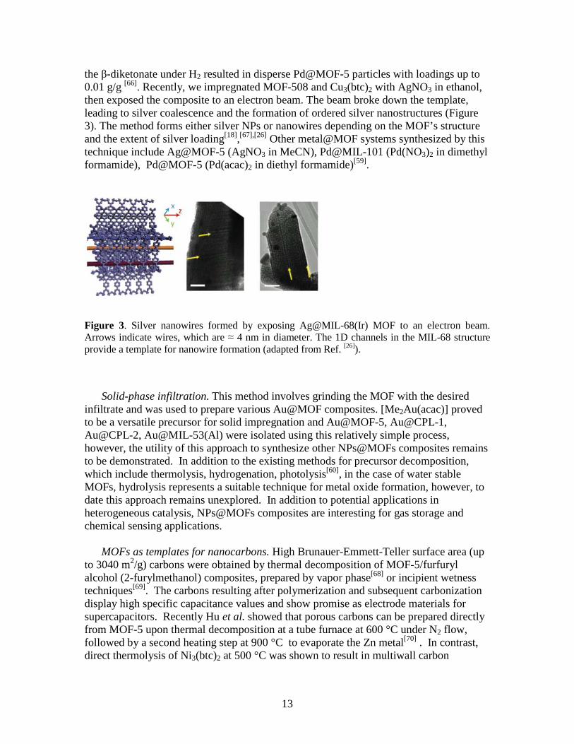
the β-diketonate under H2 resulted in disperse Pd@MOF-5 particles with loadings up to 0.01 g/g [66]. Recently, we impregnated MOF-508 and Cu3(btc)2 with AgNO3 in ethanol, then exposed the composite to an electron beam. The beam broke down the template, leading to silver coalescence and the formation of ordered silver nanostructures (Figure 3). The method forms either silver NPs or nanowires depending on the MOF’s structure and the extent of silver loading[18],[67],[26] Other metal@MOF systems synthesized by this technique include Ag@MOF-5 (AgNO3 in MeCN), Pd@MIL-101 (Pd(NO3)2 in dimethyl formamide), Pd@MOF-5 (Pd(acac)2 in diethyl formamide)[59].
Figure 3. Silver nanowires formed by exposing Ag@MIL-68(Ir) MOF to an electron beam. Arrows indicate wires, which are ≈ 4 nm in diameter. The 1D channels in the MIL-68 structure provide a template for nanowire formation (adapted from Ref. [26]).
Solid-phase infiltration. This method involves grinding the MOF with the desired
infiltrate and was used to prepare various Au@MOF composites. [Me2Au(acac)] proved to be a versatile precursor for solid impregnation and Au@MOF-5, Au@CPL-1, Au@CPL-2, Au@MIL-53(Al) were isolated using this relatively simple process, however, the utility of this approach to synthesize other NPs@MOFs composites remains to be demonstrated. In addition to the existing methods for precursor decomposition, which include thermolysis, hydrogenation, photolysis[60], in the case of water stable MOFs, hydrolysis represents a suitable technique for metal oxide formation, however, to date this approach remains unexplored. In addition to potential applications in heterogeneous catalysis, NPs@MOFs composites are interesting for gas storage and chemical sensing applications.
MOFs as templates for nanocarbons. High Brunauer-Emmett-Teller surface area (up to 3040 m2/g) carbons were obtained by thermal decomposition of MOF-5/furfuryl alcohol (2-furylmethanol) composites, prepared by vapor phase[68] or incipient wetness techniques[69]. The carbons resulting after polymerization and subsequent carbonization display high specific capacitance values and show promise as electrode materials for supercapacitors. Recently Hu et al. showed that porous carbons can be prepared directly from MOF-5 upon thermal decomposition at a tube furnace at 600 °C under N2 flow, followed by a second heating step at 900 °C to evaporate the Zn metal[70] . In contrast, direct thermolysis of Ni3(btc)2 at 500 °C was shown to result in multiwall carbon
14
nanotubes[71]. In this case, the Ni-MOF has a dual purpose: it serves as a carbon source, but also provides the catalyst (Ni) required for the nanotube growth.
Polymers@MOF. One of the most intriguing developments in the field of MOF composite structures is the in-situ formation of polymer strands within MOF pores reported by Kitagawa and coworkers.[72] In this work, the monomer precursor is infiltrated into the nanopores by immersing MOF crystals in the liquid monomer and if needed, a radical initiator. Polymerization is then accomplished by heating the composite material. MOF composites containing vinyl-based polymers such as styrene, methyl methacrylate, and vinyl acetate can be created[73]. Because MOF pores constrain polymerization, control of molecular-weight and stereochemistry are feasible. In addition, formation of single polymer strands is possible. Not only does this provide a new platform for probing the dynamics of polymer chains, it could be valuable for device applications. Conceivably, electrically conducting polymers within individual MOF channels could enable addressability at the single-nanopore level. Polyacetylene formation was demonstrated by Uemura et al.,[74] accomplishing the initial step toward realizing this concept.
A MOF-device roadmap
The development of the International Technology Roadmap for Semiconductors (ITRS) in the 1980s lead to much collaborative and highly focused work with the objective of solving critical problems inhibiting the advance of microelectronics manufacturing. Although MOFs and related materials are obviously much less advanced than the materials used in semiconductors, the success of the semiconductor suggests that a roadmap for development of MOF-based devices could serve a similar purpose. This is particularly true, we believe, because the field must move beyond the synthetic and structural aspects to engage experts in other fields, such as materials science, physics, and electrical engineering to realize the use of MOFs in electronic devices. The discussion above provides much of the information needed to determine the development status of key elements required in molecular- and nanoscale-electronics. Based on this information, we here propose a roadmap that can serve as a starting point for addressing the complex problems that must be solved. This proposal is in no way intended to be definitive. Its purpose, as remarked in the introduction, is to stimulate thinking in this area and raise awareness within other fields.
We identified five broad areas pertinent to device fabrication into which we subdivide the roadmap. These are:
1. Fundamental properties 2. Thin film growth and processing 3. MOF hybrids and multilevel structures 4. Device integration 5. Manufacturing issues

15
The key problems within each area are summarized in the discussion below. Because MOFs are so new, many of these problems fall within the category of basic research. Consequently, it is not possible to assign target dates for their solution, as is the case in the ITRS. Therefore, our proposed roadmap, shown schematically in Figure 4, begins with the status of research as of 2010. To estimate relative progress in each area, we performed literature searches using various representative terms and looking for their coincidence with the terms “metal-organic framework” AND “nanoporous coordination polymer.” One of the ten topics searched was gas storage and sorption, for which nearly 1200 articles were found. Of the many applications proposed for MOFs, this is by far the best understood, to the point that rational design is possible. We used this number as an indication of “mature” understanding and normalized the numbers for all other topics to this value. In the discussion below, we also use silicon and commercially available conducting polymers such as polythiophene. Although much different from MOFs, Si represents an industry standard, and the properties of competing materials must exceed those of silicon in some way to gain acceptance. Organic electronics are a rapidly expanding area and bear some similarity to MOFs.
Figure 4. Progress in technical areas relevant to MOF-based devices. Plot shows number of journal articles in each area, normalized to the number of articles for gas sorption, a relatively mature area. Numbers on the right are total number of articles found.
Fundamental properties. MOFs are most thoroughly characterized with respect to their gas sorption and surface area-related properties. In contrast, very little work has been done to determine the values of fundamental properties, knowledge of which is crucial to successful integration. These properties fall into three general categories: 1) electronic; 2) mechanical and thermal; and 3) optical properties.
Electrical properties. Electronic properties of importance include energy bandgap, electron and hole mobility and dielectric constant. In addition to these properties, understanding of defects and their relationship to these properties must be understood, since they likely will limit the ultimate performance of a device. The materials properties relevant to electronic applications are dictated by the requirements of the field effect transistor (FET), the basic device building block for modern electronics. In a FET, a gate

16
electrode modulates the current through a semiconductor channel connected by source and drain electrodes. The FET performance is determined by the carrier mobility, source and drain contact resistance, and the capacitance of the gate electrode (high capacitance allows moderate gate voltage to swing large source-drain current).[75] Si is the preeminent materials for FET fabrication because of its bandgap of 1.1 eV, high carrier mobility, availability of multiple n- and p-type dopants, environmental stability, stable oxide, and high terrestrial abundance. However, Si based device fabrication requires enormous capital investment and Si is not compatible with a variety of low cost, flexible, transparent, and low melting temperature substrates. For these reasons, alternative materials including polymers, organic molecules, and more recently nanotubes and nanowires have been gaining a lot of attention for various emerging applications. Commercially available polymers based on polythiophene (p-type) and polycyanoterephthalylidene (n-type) as well as oligomers such anthracence (p-type) and cyano substituted perylene (n-type) can have mobilities comparable to amorphous Si (≈1 cm2/Vs) and are being actively incorporated into electronic devices including complementary metal oxide semiconductor (CMOS) logic.[76] However, achieving mobilities similar to crystalline Si (≈1000 cm2/Vs) in these materials is unlikely, since charge transport is dominated by intermolecular carrier hopping.
The long-range crystalline order of MOFs implies that charge transport through delocalized conduction and valence bands typical of crystalline inorganic semiconductors is possible. Emergence of delocalized bands in MOFs will require that the π orbitals in the linker groups overlap effectively with the metal d orbitals. Such overlap is absent in the majority of MOFs where carboxylate oxygen atoms are coordinated to the metal center through σ bonds, and therefore most MOFs are electrical insulators. An example of a MOF-5 crystal drop-cast on a Au-coated slide and electrically probed inside of a scanning electron microscope is shown in Figure 5. This and similar crystallites were biased to over 150 V without any measurable current (pA resolution) corresponding to a breakdown field strength of over 104 V/cm, even after bombardment with a 1 kV electron beam. Note that at such high bias, contact resistance does not contribute substantially to the observed transport characteristics.
Figure 5. (a) Scanning electron microscope (SEM) image of MOF-5 crystal probed in SEM (no measurable current at 150 V); (b) Ag@MOF-508 crystal probed in SEM (c) measured I-V characteristics for the MOF-508 crystal.
Our observation that MOF-5 (IRMOF-1) is an excellent insulator is in contrast to several recent reports where MOF-5 was referred to as ‘semiconducting.’[77] This label was attributed based on the MOF-5 photoluminescence spectra which indicate a bandgap

17
of ≈2 eV. Although the terephthalate ligand may ‘sensitize’ the Zn4O13 quantum dots, these luminescent centers remain electrically isolated, and the crystal, as a whole, is an excellent insulator. We subsequently discovered that ZnO nanoparticles co-formed with MOF-5 during synthesis are the source of the anomalously low optical bandgap. Other factors, such as trapped solvent and partial lattice collapse, can affect spectrum of MOF luminescence, indicating that methods in addition to optical spectroscopy must be employed to accurately determine MOF bandgaps. [78] Recent calculations by Zagorodniy et al. confirm that IRMOFs are excellent low-k dielectrics. They computed dielectric constants for thirty IRMOFs and find them to be less than 2 in all cases, with three of these possessing a desirable combination of bulk modulus and bandgap energy required for ultralow-k dielectrics.[79] Alternatively, electrical measurements by several groups demonstrate that MOFs can have high dielectric constants, some of which are found to be ferroelectrics.[80]
A few conducting MOFs are known, however. A Cu-Cu dithiophene framework (Cu[Cu(pdt)2] (pdt ) 2,3-pyrazinedithiolate)) exhibits p-type conductivity of 6 × 10⁻⁴ S cm-1 at 300 K. This material does not have permanent porosity, however.[12c] Recently Kobayashi et al. synthesized a nickel-substituted version of this MOF that is porous and has similar electrical properties. Conductivity in this frameworks occurs through an oxidation-reduction process; for example, in the work of Kobayashi et al., a Cu(I)—Ni(II) pair is involved (Figure 6).[12b] Another potential route to conductivity was demonstrated by Fuma et al. in which a mixed oxidation state compound [{Rh2(acam)4}3(μ3-Cl)2]‚4H2O (acam = acetamide) with a honeycomb structure displays a five-order of magnitude conductivity increase upon hydration.[81] ESR results indicate that electrons hop over the Rh2 units with a low activation barrier.
Figure 6. P-type semiconducting nanoporous MOF, illustrating the electron transfer process thought to be responsible for the semiconducting properties (used with permission from ref. [12b]).
It is unclear how general either of the strategies just described might be. However, achieving higher electronic conductivity in MOFs will require the synthesis of new compounds. The Cu-Cu and Cu-Ni MOFs demonstrate that bandgap tuning is feasible (≈1 eV and ≈2 eV, respectively), in the useful range for a number of optoelectronic applications. Recent computational investigations also suggest that substituting Co for Zn can be used to decrease the bandgap of IRMOF-1.[25b] Alternatively, modifying the linker
18
structure could lead to better charge transfer between linker and the metal cations of the framework. One possible route is to replace the carboxylate terminating linkers with isocyanide groups. The dye Prussian Blue, a mixed valence crystalline compound with Fe(II) and Fe(III) ions coordinated with isocyanide ligands, is electrically conducting.[82] Perhaps MOFs based on terephthalonitrile linkers will also exhibit conductivity. An alternate approach is to introduce conducting phases into the MOF channels. A variety of metal and inorganic semiconductor nanocrystals, as well as polymers, have now been successfully incorporated into different MOFs (see discussion above). Provided that these nanocrystals are sufficiently close to allow charge hopping, electrical conduction can arise. In Figures 5b and 5c we show very preliminary but encouraging results of electrically conductivity measured in MOF-508 crystal infused with AgNO3 and later thermally annealed at 300 oC. Other nanomaterials which could potentially be introduced into MOFs to modify electronic transport include carbon nanotubes and conducting polymers.
Computational methods may prove to be a viable alternative to experiments to at least determine trends in MOF optical properties. Accurate predictions of thermodynamic and possibly mechanical properties may be feasible (see below). However, similarly accurate electronic properties such as the bandgap will be difficult to achieve, even with large parallel computers. MOFs have very large unit cells, making any computation of MOF properties highly expensive. All-electron quantum-chemistry methods are infeasible for such large systems. Density Functional Theory (DFT) methods using periodic boundary conditions have been used to predict the electronic structure of MOFs.[83] However, it is well known that such methods typically underestimate excited state energies by as much as a factor of two. High-accuracy methods, such as Quantum Monte Carlo (QMC), DFT+U, and GW are not feasible for systems with such large numbers of electrons (practical QMC calculations currently do not exceed 1000 electrons; one formula unit of IRMOF-1 (Zn4O(BDC)3 has 760 electrons and 106 atoms). In this regard, MOFs are much more challenging than traditional electronic materials, which are typically much smaller (the unit cell of silicon has only 2 atoms, for example). Consequently, even though accurate prediction of MOF gas sorption properties is now feasible, our assessment of the literature indicates that computational methods are at an early stage of development with respect to predicting MOF properties relevant to electronic devices.
Thermal properties. Thermal stability is important to avoid device failure as a result of heat generated during operation or as a result of operating in high-temperature environments. Very little work involving MOFs has been reported in this area, considering the large number of MOFs that have been synthesized.[84] Computational methods can be used to predict temperature-dependent thermodynamic properties (heat capacity, enthalpy, and entropy) and thermal conductivity with using DFT[85] and atomistic methods.[86] We are aware of only one report involving MOFs: the prediction of the thermal conductivity of IRMOF-1 using molecular dynamics.[84a] Not surprisingly, it is a poor thermal conductor.
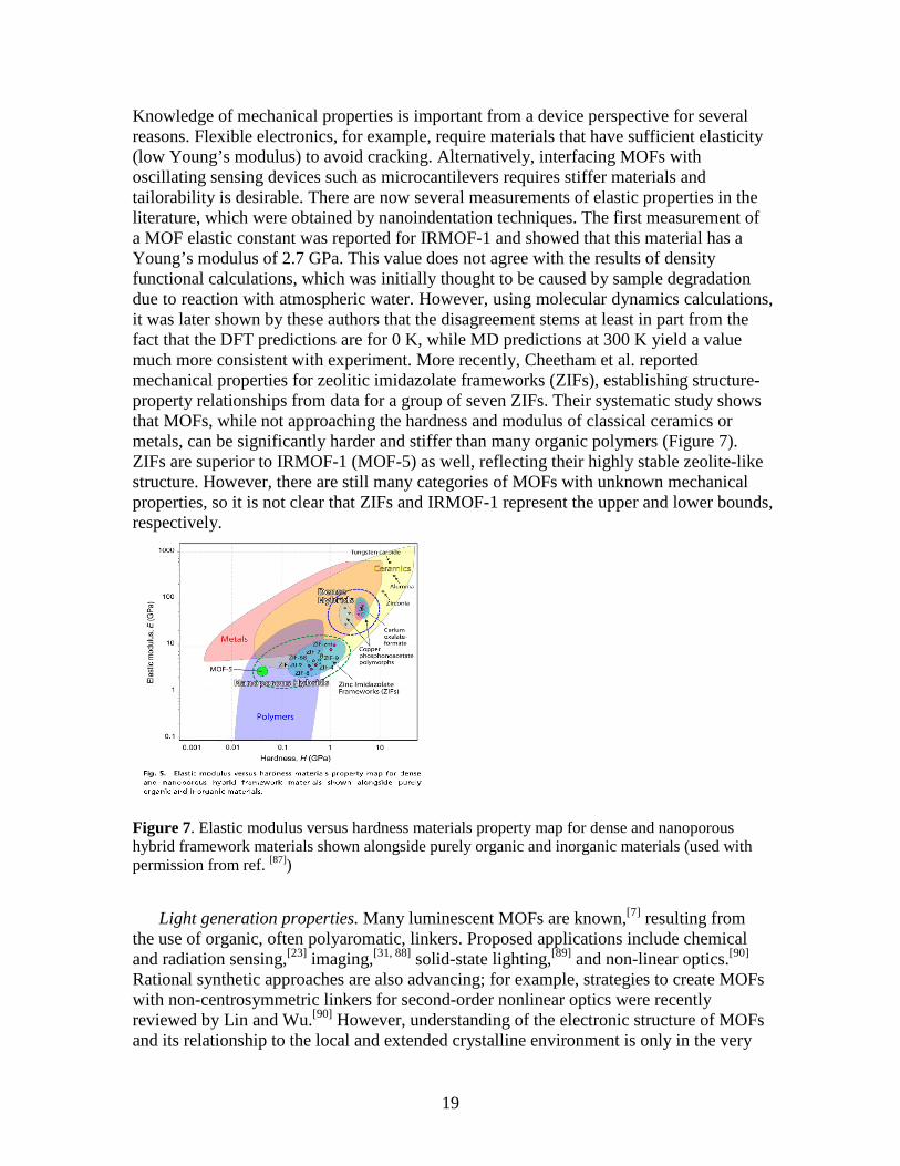
Mechanical properties. Mechanical properties of MOFs are somewhat better characterized than their electrical properties; a review of the topic was recently published.
19
Knowledge of mechanical properties is important from a device perspective for several reasons. Flexible electronics, for example, require materials that have sufficient elasticity (low Young’s modulus) to avoid cracking. Alternatively, interfacing MOFs with oscillating sensing devices such as microcantilevers requires stiffer materials and tailorability is desirable. There are now several measurements of elastic properties in the literature, which were obtained by nanoindentation techniques. The first measurement of a MOF elastic constant was reported for IRMOF-1 and showed that this material has a Young’s modulus of 2.7 GPa. This value does not agree with the results of density functional calculations, which was initially thought to be caused by sample degradation due to reaction with atmospheric water. However, using molecular dynamics calculations, it was later shown by these authors that the disagreement stems at least in part from the fact that the DFT predictions are for 0 K, while MD predictions at 300 K yield a value much more consistent with experiment. More recently, Cheetham et al. reported mechanical properties for zeolitic imidazolate frameworks (ZIFs), establishing structure-property relationships from data for a group of seven ZIFs. Their systematic study shows that MOFs, while not approaching the hardness and modulus of classical ceramics or metals, can be significantly harder and stiffer than many organic polymers (Figure 7). ZIFs are superior to IRMOF-1 (MOF-5) as well, reflecting their highly stable zeolite-like structure. However, there are still many categories of MOFs with unknown mechanical properties, so it is not clear that ZIFs and IRMOF-1 represent the upper and lower bounds, respectively.
Figure 7. Elastic modulus versus hardness materials property map for dense and nanoporous hybrid framework materials shown alongside purely organic and inorganic materials (used with permission from ref. [87])
Light generation properties. Many luminescent MOFs are known,[7] resulting from the use of organic, often polyaromatic, linkers. Proposed applications include chemical and radiation sensing,[23] imaging,[31, 88] solid-state lighting,[89] and non-linear optics.[90] Rational synthetic approaches are also advancing; for example, strategies to create MOFs with non-centrosymmetric linkers for second-order nonlinear optics were recently reviewed by Lin and Wu.[90] However, understanding of the electronic structure of MOFs and its relationship to the local and extended crystalline environment is only in the very

20
early stages of development. Only a few band structure calculations have been performed (see above) and systematic investigations of MOF luminescence have not been performed. The role of linker orientation, interchromophore distance, and interpenetration are largely unknown. The effects of impurities, partial lattice collapse, and intercalated solvent are only recently coming to light. We demonstrated, for example, that ZnO nanoparticles can form during synthesis of IRMOF-1 and this is highly dependent upon the method synthesis. Consequently, although over 350 articles connected in some way with this topic have been published, this is more reflective of the level of interest than the extent of scientific understanding.
Thin film growth. As discussed above, deposition of MOF thin films is a likely starting point for device fabrication. In the microelectronics industry, a great variety of thin film growth processes are in use, including chemical vapor deposition and related methods (ALD, OMVPE, etc.), both thermal and plasma-driven; physical vapor deposition (evaporation, sputtering); and liquid-phase growth methods. These have been refined to allow film thickness, composition, and microstructure to be tightly controlled. Comparable technologies are not available for MOFs and only a handful of MOFs can be grown on surfaces at all, making this an important focal point for future research. All MOF growth methods reported to date are liquid-phase processes, as discussed above.
Substrates. Since silicon is not likely to be eclipsed by another material in the foreseeable future, the ability to use it as a substrate for MOFs is essential. All MOF growth processes available today initiate growth on either an oxide (silicon dioxide or aluminum oxide) or on an intervening self-assembled monolayer (SAM) terminated with a carboxyl, hydroxyl, or amine group. For applications in which electrical contact between the MOF and silicon (or any other substrate, for that matter) is needed, placing a potentially insulating layer between the two could be fatal to device performance. Consequently, growth techniques that avoid this must be developed.
Single-crystal vs polycrystalline films. Although growth of individual MOF crystals on surfaces has been observed, this occurs over very small length scales, such that only small areas can be coated and thickness is not controllable. In the active area of a microelectronic device (i.e., at the level of individual transistors, for example), single-crystal films can be confined to very small dimensions. However, in the fabrication of other components of electronic devices, such as deposition of dielectric materials, wide-area growth methods with a high level of thickness control are needed. Here, existing solution methods for MOF growth may be inadequate because they produce polycrystalline films rather than the amorphous microstructures desirable for microelectronics. Polycrystalline films may be useable for MEMS devices, however, as long as satisfactory adhesion can be obtained.
Selective growth. This is essential for patterning MOFs on surfaces. As discussed above, MOF patterning by nucleating on gold using an intermediate SAM is feasible and provides an interface to a potential electrical contact. However, this type of SAM is undesirable not only because could interfere with electrical communication with the substrate, but also because of their low thermal stability. Clearly, patterning and film
21
growth are interdependent, since the mode of attachment likely will affect the film growth mode.
Growth rates. MOF film growth rates are currently extremely slow, typically requiring up to a day to produce films on the order of 100 nm thick. Films of this thickness may not always be needed, of course. For example, one can imagine devices in which only a few highly ordered unit cells are grown on the surface. In this case, an ALD-like MOF growth process is desirable, since this has the potential to produce conformal films in a self-limiting manner that enables tight control over layer thickness. For this to be possible, however, much more needs to be understood concerning the kinetics of nucleation. This may make both selective growth and thickness control very difficult. ALD and other film growth methods used by industry are also far more flexible in terms of the types of materials that can be deposited. While it is certainly true that process optimization for a given material is always required, current MOF growth methods must be developed from the ground up on a MOF-by-MOF basis. If the synthetic versatility of MOFs is to be available to device designers, this situation must be improved.
MOF hybrids and multilevel structures. Although there are encouraging developments with respect to forming hybrids or multilevel structures, such as the templating efforts describing above and creation of core-shell MOF structures, there is still a very long way to go before even a primitive integrated circuit involving a MOF scaffold or hybrid can be constructed. Research focused on making high-quality electrical contacts between the MOF and an underlying conducting or semiconducting pad is essential, as is developing methods to create ordered structures in which, for example, metal nanowires on one layer connect with either another MOF or a different material on another level. These methods must be compatible with pre-existing structures. Perhaps even more challenging, integration of other materials following growth of the MOF layer must not damage it; this rules out growth steps at temperatures the MOF cannot tolerate, use of acid baths or other harsh etching techniques, and possibly plasma cleaning, although the limits of MOF stability under such conditions have not be explored. Clearly, however, this is an extremely challenging area. Fortunately, extensive prior research in the area of organic electronics provides a starting point for forming comparable structures involving MOFs.[91]
Device integration. Integration of MOFs as components of functioning devices is at a very early stage of development. By integration, we mean more than a demonstration of a signal transduction mechanism, such as the observation of fluorescence quenching or the detection of a color change using laboratory instrumentation. Rather, by our definition integration implies that the MOF is an integral component of an actual device structure and that the fundamental problems of circuit design, electrical contacts, power supply, and measurement have been solved to at least a rudimentary stage. By this standard, there are only a handful of examples in the literature (discussed above), mostly involving MEMS devices in which a MOF coating was applied to a readily accessible surface. There are thus many issues that must be addressed before MOFs can be used beyond these relatively straightforward applications. Key among these include the following:
22
• Compatibility between MOF-related processing and substrate materials • Compatibility of post-MOF integration steps with the MOF, such formation of
electrical contacts (“back end of the line” in microelectronics fabrication) • Development of interface layers or chemistries to enhance MOF adhesion • Packaging • In-line analytical tools for quality control
Large-scale manufacturing issues. It may seem premature to include in the roadmap
aspects related to large-scale manufacturing of devices that incorporate MOFs, but this is an issue that must be faced eventually. This is at least a two-dimensional problem, in that not only must large quantities of material be produced, it must be produced quickly so that manufacturing throughput can be maintained. Present methods of growing bulk samples of MOFs produce no more than ≈1 g of material. Although it is encouraging that a few MOFs are now available commercially, demonstrating that large-scale synthesis is at least feasible, it is not clear how general the methods are these methods that can produce kg or larger quantities. We recently reviewed the synthetic methods reported thus far with potential for producing such quantities, which include microwave, sonochemical, and mechanochemical routes.[92] While these methods can be scaled up, it is unlikely that powders will be used to produce electronic devices. As discussed earlier, there are only a few examples of MOF growth on surfaces, and our own experience indicates that even growth of layers corresponding to a few MOF unit cells can take several hours. This area therefore represents a major obstacle to large-scale MOF integration.
Although the reactants used in most MOF syntheses present a relatively low hazard, the large quantities of solvent sometimes used are not. Solvents are not only costly, but they present handling, safety, and disposal issues. This magnitude of this problem in the semiconductor industry has lead to inclusion of a “green fab” category within the International Technology Roadmap for Semiconductors, including both intrinsic and factory integration requirements.[2]This industry is making great strides with respect to minimizing both solvent and water usage. Consequently, it is reasonable to expect that future manufacturing with MOFs will require processes that incorporate green chemistry. It will be a challenge, however, to eliminate solvent entirely and synthetic methods with potential for producing MOFs at a high rate are not readily adaptable to thin film growth.
Conclusions
MOFs offer an unusual combination of synthetic flexibility and varied properties that present many opportunities for their use in electronic devices. Although their use in devices so far is confined to sensors, there are many examples of MOFs with tunable bandgap, both ultralow-k and high-k dielectric constants, varied magnetic properties, luminosity, and semiconducting behavior (in a few cases), suggesting a range of properties unmatched by any other class of materials. Combining these with their highly ordered nanoporous structure creates the potential for electronics and self-assembly with

23
single-digit nanometer-scale resolution. Many problems must be solved before this nanoelectronic Valhalla can be attained, however. Not the least of these is the lack of generalized fabrication methods by which defect-free MOF thin films can be grown across length scales meaningful for electronic applications. Solving this problem will enable MOFs to be used to the fullest extent of their properties, as well as allowing the necessary integration with other materials needed to complete the device. An even more fundamental need is for information concerning MOF electronic properties, few of which have been characterized in any detail. While these challenges are daunting, the potential for impact in areas ranging from photovoltaics to molecular computing is a strong motivator for expanding this area of MOF research. If the rapid progress with respect to understanding gas adsorption in these materials is any indication, it is likely that considerable advances toward these goals will be made in the near future, opening an exciting new subdiscipline in the field of supramolecular materials.
Acknowledgements
The authors gratefully acknowledge the financial support of the Defense Threat Reduction Agency under contract 074325I-0; the US Dept. of Energy Office of Proliferation Detection Advanced Materials Program; and the Sandia Laboratory Directed Research and Development Program. Sandia National Laboratories is a multi-program laboratory managed and operated by Sandia Corporation, a wholly owned subsidiary of Lockheed Martin Corporation, for the U.S. Department of Energy's National Nuclear Security Administration under contract DE-AC04-94AL85000.
[1] E. A. Costner, M. W. Lin, W. L. Jen, C. G. Willson, Annu. Rev. Mater. Res. 2009, 39, 155-180.
[2] International Roadmap for Semiconductors, Semiconductor Industry Association, 2007.
[3] a) S. Srivastava, N. A. Kotov, Soft Matter 2009, 5, 1146-1156; b) A. R. Tao, J. X. Huang, P. D. Yang, Acc. Chem. Res. 2008, 41, 1662-1673; c) S. Toksoz, H. Acar, M. O. Guler, Soft Matter 2010, 6, 5839-5849; d) W. X. Zhang, S. H. Yang, Acc. Chem. Res. 2009, 42, 1617-1627.
[4] a) K. Ariga, A. Vinu, Q. M. Ji, O. Ohmori, J. P. Hill, S. Acharya, J. Koike, S. Shiratori, Angew. Chem. Int. Ed. Eng. 2008, 47, 7254-7257; b) L. M. Bronstein, Colloid Chem. 1 2003, 226, 55-89; c) Q. S. Huo, D. I. Margolese, U. Ciesla, P. Y. Feng, T. E. Gier, P. Sieger, R. Leon, P. M. Petroff, F. Schuth, G. D. Stucky, Nature 1994, 368, 317-321; d) G. T. Li, S. Bhosale, T. Y. Wang, Y. Zhang, H. S. Zhu, K. H. Fuhrhop, Angew. Chem. Int. Ed. Eng. 2003, 42, 3818-3821; e) C. R. Martin, Science 1994, 266, 1961-1966; f) R. Ruiz, H. M. Kang, F. A. Detcheverry, E. Dobisz, D. S. Kercher, T. R. Albrecht, J. J. de Pablo, P. F. Nealey, Science 2008, 321, 936-939; g) Y. Wang, A. S. Angelatos, F. Caruso, Chem. Mater. 2008, 20, 848-858; h) Z. S. Zhang, S. Y. Zhang, W. R. Li, Prog. Chem. 2004, 16, 26-34.
[5] X. A. Lin, N. R. Champness, M. Schroder, in Functional Metal-Organic Frameworks: Gas Storage, Separation and Catalysis, Vol. 293, 2010, pp. 35-76.

24
[6] J. R. Li, R. J. Kuppler, H. C. Zhou, Chem. Soc. Rev. 2009, 38, 1477-1504. [7] M. D. Allendorf, C. A. Bauer, R. K. Bhakta, R. J. T. Houk, Chem. Soc. Rev. 2009,
38, 1330-1352. [8] J. Lee, O. K. Farha, J. Roberts, K. A. Scheidt, S. T. Nguyen, J. T. Hupp, Chem. Soc.
Rev. 2009, 38, 1450-1459. [9] H. M. El-Kaderi, J. R. Hunt, J. L. Mendoza-Cortes, A. P. Cote, R. E. Taylor, M.
O'Keeffe, O. M. Yaghi, Science 2007, 316, 268-272. [10] A. Phan, C. J. Doonan, F. J. Uribe-Romo, C. B. Knobler, M. O'Keeffe, O. M. Yaghi,
Acc. Chem. Res. 2010, 43, 58-67. [11]a) M. S. El-Shall, V. Abdelsayed, A. Khder, H. M. A. Hassan, H. M. El-Kaderi, T. E.
Reich, J. Mater. Chem. 2009, 19, 7625-7631; b) D. Esken, X. Zhang, O. I. Lebedev, F. Schroder, R. A. Fischer, J. Mater. Chem. 2009, 19, 1314-1319; c) R. J. T. Houk, B. W. Jacobs, F. El Gabaly, N. N. Chang, A. A. Talln, D. D. Graham, S. D. House, I. M. Robertson, M. D. Allendorf, Nano Lett. 2009, 9, 3413-3418; d) H. R. Moon, J. H. Kim, M. P. Suh, Angew. Chem. Int. Ed. Eng. 2005, 44, 1261-1265; e) M. Muller, S. Hermes, K. Kaehler, M. W. E. van den Berg, M. Muhler, R. A. Fischer, Chem. Mater. 2008, 20, 4576-4587.
[12]a) M. Alvaro, E. Carbonell, B. Ferrer, F. Xamena, H. Garcia, Chem. Eur. J. 2007, 13, 5106-5112; b) Y. Kobayashi, B. Jacobs, M. D. Allendorf, J. R. Long, Chem. Mater. 2010, 22, 4120-4122; c) S. Takaishi, M. Hosoda, T. Kajiwara, H. Miyasaka, M. Yamashita, Y. Nakanishi, Y. Kitagawa, K. Yamaguchi, A. Kobayashi, H. Kitagawa, Inorg. Chem. 2008, 48, 9048.
[13] a) B. Civalleri, F. Napoli, Y. Noel, C. Roetti, R. Dovesi, CrystEngComm 2006, 8, 364-371; b) M. Fuentes-Cabrera, D. M. Nicholson, B. G. Sumpter, M. Widom, J. Chem. Phys. 2005, 123; c) A. Kuc, A. Enyashin, G. Seifert, J. Phys. Chem. B 2007, 111, 8179-8186.
[14] M. Kurmoo, Chem. Soc. Rev. 2009, 38, 1353-1379. [15]a) Z. G. Guo, R. Cao, X. Wang, H. F. Li, W. B. Yuan, G. J. Wang, H. H. Wu, J. Li, J.
Amer. Chem. Soc. 2009, 131, 6894-+; b) Y. M. Xie, J. H. Liu, X. Y. Wu, Z. G. Zhao, Q. S. Zhang, F. Wang, S. C. Chen, C. Z. Lu, Cryst. Growth Des. 2008, 8, 3914-3916.
[16] a) S. Bureekaew, S. Horike, M. Higuchi, M. Mizuno, T. Kawamura, D. Tanaka, N. Yanai, S. Kitagawa, Nat. Mater. 2009, 8, 831-836; b) J. A. Hurd, R. Vaidhyanathan, V. Thangadurai, C. I. Ratcliffe, I. L. Moudrakovski, G. K. H. Shimizu, Nat. Chem. 2009, 1, 705-710; c) M. Sadakiyo, T. Yamada, H. Kitagawa, J. Amer. Chem. Soc. 2009, 131, 9906-+; d) J. M. Taylor, R. K. Mah, I. L. Moudrakovski, C. I. Ratcliffe, R. Vaidhyanathan, G. K. H. Shimizu, J. Amer. Chem. Soc. 2010, 132, 14055-14057.
[17] a) A. J. Fletcher, K. M. Thomas, M. J. Rosseinsky, J. Solid State Chem. 2005, 178, 2491; b) K. Uemura, R. Matsuda, S. Kitagawa, J. Solid State Chem. 2005, 178, 2420.
[18] M. D. Allendorf, R. J. T. Houk, L. Andruszkiewicz, A. A. Talin, J. Pikarsky, A. Choudhury, K. A. Gall, P. J. Hesketh, J. Amer. Chem. Soc. 2008, 130, 14404-+.
[19]E. Biemmi, A. Darga, N. Stock, T. Bein, Microporous Mesoporous Mater. 2008, 114, 380-386.
[20]S. Achmann, G. Hagen, J. Kita, I. M. Malkowsky, C. Kiener, R. Moos, Sensors 2009, 9, 1574-1589.
[21] L. E. Kreno, J. T. Hupp, R. P. Van Duyne, Anal. Chem. 2010, 82, 8042-8046.

25
[22] G. Lu, J. T. Hupp, J. Amer. Chem. Soc. 2010, 132, 7832-+. [23] F. P. Doty, C. A. Bauer, A. J. Skulan, P. G. Grant, M. D. Allendorf, Adv. Mater.
2009, 21, 95-101. [24] G. J. Halder, C. J. Kepert, B. Moubaraki, K. S. Murray, J. D. Cashion, Science 2002,
298, 1762-1765. [25] a) Y. Chen, Z. O. Wang, Z. G. Ren, H. X. Li, D. X. Li, D. Liu, Y. Zhang, J. P. Lang,
Cryst. Growth Des. 2009, 9, 4963-4968; b) J. H. Choi, Y. J. Choi, J. W. Lee, W. H. Shin, J. K. Kang, Phys. Chem. Chem. Phys. 2009, 11, 628-631.
[26] B. W. Jacobs, R. J. T. Houk, M. R. Anstey, S. D. House, I. M. Robertson, A. A. Talin, M. D. Allendorf, Chem. Sci. 2011.
[27] a) S. Hermes, F. Schröder, R. Chelmowski, C. Wöll, R. A. Fischer, J. Amer. Chem. Soc. 2005, 127, 13744-13745; b) S. Hermes, T. Witte, T. Hikov, D. Zacher, S. Bahnmuller, G. Langstein, K. Huber, R. A. Fischer, J. Amer. Chem. Soc. 2007, 129, 5324-+; c) E. Biemmi, C. Scherb, T. Bein, J. Amer. Chem. Soc. 2007, 129, 8054-8055; d) C. Scherb, A. Schödel, T. Bein, Angew. Chem. Int. Ed. Eng. 2008, 47, 5777-5779; e) M. Arnold, P. Kortunov, D. J. Jones, Y. Nedellec, J. Kärger, J. Caro, Eur. J. Inorg. Chem. 2007, 2007, 60-64; f) S. Hermes, D. Zacher, A. Baunemann, C. Woll, R. A. Fischer, Chem. Mater. 2007, 19, 2168-2173; g) D. Zacher, A. Baunemann, S. Hermes, R. A. Fischer, J. Mater. Chem. 2007, 17, 2785-2792; h) O. Shekhah, H. Wang, S. Kowarik, F. Schreiber, M. Paulus, M. Tolan, C. Sternemann, F. Evers, D. Zacher, R. A. Fischer, C. Woll, J. Amer. Chem. Soc. 2007, 129, 15118-+; i) O. Shekhah, H. Wang, T. Strunskus, P. Cyganik, D. Zacher, R. Fischer, C. Wöll, Langmuir 2007, 23, 7440-7442; j) M. Kubo, W. Chaikittisilp, T. Okubo, Chem. Mater. 2008, 20, 2887-2889; k) R. Ameloot, L. Stappers, J. Fransaer, L. Alaerts, B. F. Sels, D. E. De Vos, Chem. Mater. 2009, 21, 2580-2582; l) R. Ameloot, L. Pandey, M. Van der Auweraer, L. Alaerts, B. F. Sels, D. E. De Vos, Chem. Comm. 2010, 46, 3735-3737.
[28] a) A. Demessence, P. Horcajada, C. Serre, C. Boissiere, D. Grosso, C. Sanchez, G. Ferey, Chem. Comm. 2009, 7149-7151; b) P. Horcajada, C. Serre, D. Grosso, C. Boissiere, S. Perruchas, C. Sanchez, G. Ferey, Adv. Mater. 2009, 21, 1931-1935; c) M. C. McCarthy, V. Varela-Guerrero, G. V. Barnett, H.-K. Jeong, Langmuir, 26, 14636-14641.
[29] a) J. Gascon, S. Aguado, F. Kapteijn, Microporous Mesoporous Mater. 2008, 113, 132-138; b) Y. Yoo, Z. P. Lai, H. K. Jeong, Microporous Mesoporous Mater. 2009, 123, 100-106; c) R. Ranjan, M. Tsapatsis, Chem. Mater. 2009, 21, 4920-4924; d) S. R. Venna, M. A. Carreon, J. Amer. Chem. Soc. 2009, 132, 76-78; e) Y. S. Li, F. Y. Liang, H. Bux, A. Feldhoff, W. S. Yang, J. Caro, Angew. Chem. Int. Ed. Eng. 2010, 49, 548-551; f) Y. S. Li, H. Bux, A. Feldhoff, G. L. Li, W. S. Yang, J. Caro, Adv. Mater. 2010, 22, 3322-+.
[30] D. Zacher, O. Shekhah, C. Woll, R. A. Fischer, Chem. Soc. Rev. 2009, 38, 1418-1429.
[31] A. M. Spokoyny, D. Kim, A. Sumrein, C. A. Mirkin, Chem. Soc. Rev. 2009, 38, 1218-1227.
[32]T. Tsuruoka, S. Furukawa, Y. Takashima, K. Yoshida, S. Isoda, S. Kitagawa, Angew. Chem. Int. Ed. Eng. 2009, 48, 4739-4743.

26
[33]R. Makiura, S. Motoyama, Y. Umemura, H. Yamanaka, O. Sakata, H. Kitagawa, Nat. Mater. 2010, 9, 565-571.
[34] R. Makiura, H. Kitagawa, Eur. J. Inorg. Chem. 2010, 3715-3724. [35] H. Guo, G. Zhu, I. J. Hewitt, S. Qiu, J. Amer. Chem. Soc. 2009, 131, 1646-1647. [36] X. Q. Zou, G. S. Zhu, I. J. Hewitt, F. X. Sun, S. L. Qiu, Dalton Trans. 2009, 3009-
3013. [37] A. Schoedel, C. Scherb, T. Bein, Angew. Chem. Int. Ed. Eng. 2010, 49, 7225-7228. [38] M. C. McCarthy, V. Varela-Guerrero, G. V. Barnett, H. K. Jeong, Langmuir 2010,
26, 14636-14641. [39] A. Huang, W. Dou, J. r. Caro, J. Amer. Chem. Soc. 2010, 132, 15562-15564. [40] a) O. Shekhah, H. Wang, M. Paradinas, C. Ocal, B. Schupbach, A. Terfort, D.
Zacher, R. A. Fischer, C. Woll, Nat. Mater. 2009, 8, 481-484; b) O. Shekhah, H. Wang, D. Zacher, R. A. Fischer, C. Woll, Angew. Chem. Int. Ed. Eng. 2009, 48, 5038-5041; c) M. Darbandi, H. K. Arslan, O. Shekhah, A. Bashir, A. Birkner, C. Woll, Phys. Stat. Sol. 2010, 4, 197-199; d) O. Shekhah, Materials 2010, 3, 1302-1315; e) K. Yusenko, M. Meilikhov, D. Zacher, F. Wieland, C. Sternemann, X. Stammer, T. Ladnorg, C. Woll, R. A. Fischer, CrystEngComm 2010, 12, 2086-2090.
[41]M. S. El-Shall, V. Abdelsayed, A. E. R. S. Khder, H. M. A. Hassan, H. M. El-Kaderi, T. E. Reich, J. Mater. Chem. 2009, 19, 7625-7631.
[42] C. Munuera, O. Shekhah, H. Wang, C. Woll, C. Ocal, Phys. Chem. Chem. Phys. 2008, 10, 7257-7261.
[43] R. E. Morris, Chemphyschem 2009, 10, 327-329. [44] M. Eddaoudi, J. Kim, N. Rosi, D. Vodak, J. Wachter, M. O'Keeffe, O. M. Yaghi,
Science 2002, 295, 469-472. [45] O. M. Yaghi, M. O'Keeffe, N. W. Ockwig, H. K. Chae, M. Eddaoudi, J. Kim, Nature
2003, 423, 705-714. [46] K. Koh, A. G. Wong-Foy, A. J. Matzger, Chem. Comm. 2009, 6162-6164. [47] S. Furukawa, K. Hirai, K. Nakagawa, Y. Takashima, R. Matsuda, T. Tsuruoka, M.
Kondo, R. Haruki, D. Tanaka, H. Sakamoto, S. Shimomura, O. Sakata, S. Kitagawa, Angew. Chem. Int. Ed. Eng. 2009, 48, 1766-1770.
[48] Y. Yoo, H. K. Jeong, Cryst. Growth Des. 2010, 10, 1283-1288. [49] M. Muller, A. Devaux, C. H. Yang, L. De Cola, R. A. Fischer, Photochem.
Photobiol. Sci. 2010, 9, 846-853. [50] a) S. M. Cohen, Chem. Sci. 2010, 1, 32-36; b) K. K. Tanabe, S. M. Cohen, Chem.
Soc. Rev. 2011, 40, 498-519; c) Z. Q. Wang, S. M. Cohen, Chem. Soc. Rev. 2009, 38, 1315-1329.
[51] a) B. L. Chen, S. C. Xiang, G. D. Qian, Acc. Chem. Res. 2010, 43, 1115-1124; b) K. Gedrich, I. Senkovska, N. Klein, U. Stoeck, A. Henschel, M. R. Lohe, I. A. Baburin, U. Mueller, S. Kaskel, Angew. Chem. Int. Ed. Eng. 2010, 49, 8489-8492; c) Z. Y. Guo, H. Wu, G. Srinivas, Y. M. Zhou, S. C. Xiang, Z. X. Chen, Y. T. Yang, W. Zhou, M. O'Keeffe, B. L. Chen, Angew. Chem. Int. Ed. Eng. 2011, 50, 3178-3181; d) A. Mallick, S. Saha, P. Pachfule, S. Roy, R. Banerjee, J. Mater. Chem. 2010, 20, 9073-9080; e) J. R. Karra, K. S. Walton, Langmuir 2008, 24, 8620-8626; f) H. Wu, W. Zhou, T. Yildirim, J. Amer. Chem. Soc. 2009, 131, 4995-5000; g) B. L. Chen, N. W. Ockwig, A. R. Millward, D. S. Contreras, O. M. Yaghi, Angew. Chem. Int. Ed.

27
Eng. 2005, 44, 4745-4749; h) B. L. Chen, Y. Yang, F. Zapata, G. N. Lin, G. D. Qian, E. B. Lobkovsky, Adv. Mater. 2007, 19, 1693-+.
[52] a) S. S. Y. Chui, S. M. F. Lo, J. P. H. Charmant, A. G. Orpen, I. D. Williams, Science 1999, 283, 1148-1150; b) M. J. Ingleson, R. Heck, J. A. Gould, M. J. Rosseinsky, Inorg. Chem. 2009, 48, 9986-9988; c) J. L. C. Rowsell, O. M. Yaghi, J. Amer. Chem. Soc. 2006, 128, 1304-1315; d) J. G. Vitillo, L. Regli, S. Chavan, G. Ricchiardi, G. Spoto, P. D. C. Dietzel, S. Bordiga, A. Zecchina, J. Amer. Chem. Soc. 2008, 130, 8386-8396; e) S. C. Xiang, W. Zhou, J. M. Gallegos, Y. Liu, B. L. Chen, J. Amer. Chem. Soc. 2009, 131, 12415-12419.
[53] a) S. Das, H. Kim, K. Kim, J. Amer. Chem. Soc. 2009, 131, 3814-+; b) K. S. Park, Z. Ni, A. P. Cote, J. Y. Choi, R. D. Huang, F. J. Uribe-Romo, H. K. Chae, M. O'Keeffe, O. M. Yaghi, Proc. Nat. Acad. Sci. 2006, 103, 10186-10191.
[54] a) Z. Q. Wang, S. M. Cohen, J. Amer. Chem. Soc. 2007, 129, 12368-+; b) M. J. Ingleson, J. P. Barrio, J. Bacsa, C. Dickinson, H. Park, M. J. Rosseinsky, Chem. Comm. 2008, 1287-1289; c) E. Dugan, Z. Q. Wang, M. Okamura, A. Medina, S. M. Cohen, Chem. Comm. 2008, 3366-3368; d) Z. Q. Wang, S. M. Cohen, Angew. Chem. Int. Ed. Eng. 2008, 47, 4699-4702; e) M. J. Ingleson, J. P. Barrio, J. B. Guilbaud, Y. Z. Khimyak, M. J. Rosseinsky, Chem. Comm. 2008, 2680-2682.
[55] a) T. Gadzikwa, G. Lu, C. L. Stern, S. R. Wilson, J. T. Hupp, S. T. Nguyen, Chem. Comm. 2008, 5493-5495; b) T. Yamada, H. Kitagawa, J. Amer. Chem. Soc. 2009, 131, 6312-+; c) R. K. Deshpande, J. L. Minnaar, S. G. Telfer, Angew. Chem. Int. Ed. Eng. 2010, 49, 4598-4602.
[56] a) C. L. Choi, A. P. Alivisatos, Ann. Rev. Phys. Chem., Vol 61 2010, 61, 369-389; b) P. K. Jain, L. Amirav, S. Aloni, A. P. Alivisatos, J. Amer. Chem. Soc. 2010, 132, 9997-9999; c) J. Park, H. Zheng, Y. W. Jun, A. P. Alivisatos, J. Amer. Chem. Soc. 2009, 131, 13943-+; d) B. Sadtler, D. O. Demchenko, H. Zheng, S. M. Hughes, M. G. Merkle, U. Dahmen, L. W. Wang, A. P. Alivisatos, J. Amer. Chem. Soc. 2009, 131, 5285-5293; e) R. D. Robinson, B. Sadtler, D. O. Demchenko, C. K. Erdonmez, L. W. Wang, A. P. Alivisatos, Science 2007, 317, 355-358; f) D. H. Son, S. M. Hughes, Y. D. Yin, A. P. Alivisatos, Science 2004, 306, 1009-1012.
[57] a) S. L. Huang, X. X. Li, X. J. Shi, H. W. Hou, Y. T. Fan, J. Mater. Chem. 2010, 20, 5695-5699; b) T. K. Prasad, D. H. Hong, M. P. Suh, Chem. Eur. J. 2010, 16, 14043-14050.
[58] F. Schüth, Angew. Chem. Int. Ed. Eng. 2003, 42, 3604-3622. [59] M. Meilikhov, K. Yusenko, D. Esken, S. Turner, G. Van Tendeloo, R. A. Fischer,
Eur. J. Inorg. Chem. 2010, 3701-3714. [60]F. Schroeder, R. A. Fischer, in Functional Metal-Organic Frameworks: Gas Storage,
Separation and Catalysis, Vol. 293, 2010, pp. 77-113. [61] S. Hermes, M. K. Schroter, R. Schmid, L. Khodeir, M. Muhler, A. Tissler, R. W.
Fischer, R. A. Fischer, Angew. Chem. Int. Ed. Eng. 2005, 44, 6237-6241. [62] M. Muller, O. I. Lebedev, R. A. Fischer, J. Mater. Chem. 2008, 18, 5274-5281. [63] S. Proch, J. Herrmannsdorfer, R. Kempe, C. Kern, A. Jess, L. Seyfarth, J. Senker,
Chem. Eur. J. 2008, 14, 8204-8212. [64] F. Schroeder, D. Esken, M. Cokoja, M. W. E. van den Berg, O. I. Lebedev, G. van
Tendeloo, B. Walaszek, G. Buntkowsky, H. H. Limbach, B. Chaudret, R. A. Fischer, J. Amer. Chem. Soc. 2008, 130, 6119-6130.
28
[65] F. Schroeder, S. Henke, X. N. Zhang, R. A. Fischer, Eur. J. Inorg. Chem. 2009, 3131-3140.
[66] M. Sabo, A. Henschel, H. Froede, E. Klemm, S. Kaskel, J. Mater. Chem. 2007, 17, 3827-3832.
[67] R. J. T. Houk, B. W. Jacobs, F. El Gabaly, N. N. Chang, A. A. Talin, D. D. Graham, S. D. House, I. M. Robertson, M. D. Allendorf, Nano Lett. 2009, 9, 3413-3418.
[68] B. Liu, H. Shioyama, T. Akita, Q. Xu, Journal of the American Chemical Society 2008, 130, 5390-5391.
[69] B. Liu, H. Shioyama, H. Jiang, X. Zhang, Q. Xu, Carbon 2010, 48, 456-463. [70] J. A. Hu, H. L. Wang, Q. M. Gao, H. L. Guo, Carbon 2010, 48, 3599-3606. [71] L. Y. Chen, J. F. Bai, C. Z. Wang, Y. Pan, M. Scheer, X. Z. You, Chem. Comm.
2008, 1581-1583. [72] T. Uemura, N. Yanai, S. Kitagawa, Chem. Soc. Rev. 2009, 38, 1228-1236. [73] T. Uemura, Y. Ono, S. Kitagawa, Chem. Lett. 2008, 37, 616-617. [74] T. Uemura, R. Kitaura, Y. Ohta, M. Nagaoka, S. Kitagawa, Angew. Chem. Int. Ed.
Eng. 2006, 45, 4112-4116. [75] S. M. Sze, Physics of Semiconductor Devices, 2nd ed., Wiley, Hoboken, 1981. [76] T. J. Marks, MRS Bull. 2010, 35, 1018. [77] C. G. Silva, A. Corma, H. Garcia, J. Mater. Chem. 2010, 20, 3141. [78] P. L. Feng, J. J. Perry, S. Nikodemski, B. W. Jacobs, S. T. Meek, M. D. Allendorf, J.
Amer. Chem. Soc. 2010, 132, 15487-15489. [79] K. Zagorodniy, G. Seifert, H. Hermann, Appl. Phys. Lett. 2010, 97. [80] a) T. Hang, D. W. Fu, Q. Ye, H. Y. Ye, R. G. Xiong, S. D. Huang, Cryst. Growth
Des. 2009, 9, 2054-2056; b) Z. R. Qu, Q. Ye, H. Zhao, D. W. Fu, H. Y. Ye, R. G. Xiong, T. Akutagawa, T. Nakamura, Chem. Eur. J. 2008, 14, 3452-3456; c) Q. Ye, Y. M. Song, G. X. Wang, K. Chen, D. W. Fu, P. W. H. Chan, J. S. Zhu, S. D. Huang, R. G. Xiong, J. Amer. Chem. Soc. 2006, 128, 6554-6555; d) H. Zhao, Q. Ye, Z. R. Qu, D. W. Fu, R. G. Xiong, S. P. D. Huang, P. W. H. Chan, Chem. Eur. J. 2008, 14, 1164-1168.
[81] Y. Fuma, M. Ebihara, S. Kutsumizu, T. Kawamura, J. Amer. Chem. Soc. 2004, 126, 12238.
[82] J. N. Behera, D. M. D'Alessandro, N. Soheilnia, J. R. Long, Chem. Mater. 2009, 21, 1922-1926.
[83] a) D. S. Coombes, F. Cora, C. Mellot-Draznieks, R. G. Bell, J. Phys. Chem. C 2009, 113, 544-552; b) S. Keskin, J. Liu, R. B. Rankin, J. K. Johnson, D. S. Sholl, Indust. Eng. Chem. Res. 2009, 48, 2355-2371; c) M. Mattesini, J. M. Soler, F. Yndurain, Phys. Rev. B 2006, 73.
[84] a) B. L. Huang, A. J. H. McGaughey, M. Kaviany, Int. J. Heat Mass Transfer 2007, 50, 393-404; b) B. L. Huang, Z. Ni, A. Millward, A. J. H. McGaughey, C. Uher, M. Kaviany, O. Yaghi, Int. J. Heat Mass Transfer 2007, 50, 405-411; c) C. H. Jiang, L. F. Song, J. A. Zhang, L. X. Sun, F. Xu, F. Li, Q. Z. Jiao, Z. G. Sun, Y. H. Xing, Y. Du, J. L. Zeng, Z. Cao, J. Therm. Anal. Calorim. 2010, 102, 1087-1093; d) X. C. Lv, Z. C. Tan, X. H. Gao, Z. H. Zhang, L. N. Yang, J. N. Zhao, L. X. Sun, T. Zhang, Thermochim. Acta 2006, 450, 102-104; e) L. F. Song, C. H. Jiang, C. L. Jiao, J. A. Zhang, L. X. Sun, F. Xu, Q. Z. Jiao, Y. H. Xing, Y. Du, Z. Cao, F. L. Huang, J. Therm. Anal. Calorim. 2010, 102, 1161-1166; f) L. F. Song, C. H. Jiang, J. A. Zhang,
29
L. X. Sun, F. Xu, Y. Q. Tian, W. S. You, Z. Cao, L. Zhang, D. W. Yang, J. Therm. Anal. Calorim. 2010, 101, 365-370.
[85] D. S. Sholl, J. A. Steckel, Density Functional Theory: A Practical Introduction, Wiley, Hoboken, 2009.
[86] D. Frenkel, B. Smit, Understanding Molecular Simulation, Academic, San Diego, 2002.
[87] J. C. Tan, T. D. Bennett, A. K. Cheetham, Proc. Natl. Acad. Sci. 2010, 107, 9938-9943.
[88] P. Horcajada, T. Chalati, C. Serre, B. Gillet, C. Sebrie, T. Baati, J. F. Eubank, D. Heurtaux, P. Clayette, C. Kreuz, J. S. Chang, Y. K. Hwang, V. Marsaud, P. N. Bories, L. Cynober, S. Gil, G. Ferey, P. Couvreur, R. Gref, Nat. Mater. 2010, 9, 172-178.
[89] J. D. Furman, A. Y. Warner, S. J. Teat, A. A. Mikhailovsky, A. K. Cheetham, Chem. Mater. 2010, 22, 2255-2260.
[90] W. Lin, S. Wu, in Metal-Organic Frameworks: Design and Application (Ed.: L. R. MacGillivray), Wiley, Hoboken, 2010.
[91] a) F. S. Kim, G. Q. Ren, S. A. Jenekhe, Chem. Mater. 2011, 23, 682-732; b) S. S. Lee, Y. L. Loo, in Annual Review of Chemical and Biomolecular Engineering, Vol 1, Vol. 1, 2010, pp. 59-78; c) A. Operamolla, G. M. Farinola, Eur. J. Org. Chem. 2011, 423-450; d) C. Sanchez, P. Belleville, M. Popall, L. Nicole, Chem. Soc. Rev. 2011, 40, 696-753.
[92] S. T. Meek, J. A. Greathouse, M. D. Allendorf, Adv. Mater. 2011, 23, 249-267.