a silicon pixel tracker for ilc konstantin stefanov 20 november 2014
TRANSCRIPT

A Silicon Pixel Tracker for ILC
Konstantin Stefanov20 November 2014

2 20 November 2014
Introduction
• Silicon Pixel Tracker (SPT) – an idea by Chris Damerell• First presented in 2008 at the annual Asian ILC Workshop in Tohoku, Japan
– Positive reaction by the community– Further refined by Chris since– This presentation borrows a lot of his original material
• The main driver is low detector mass– Low mass is enabled by low detector power– Benefits to the forward tracker from the reduced cooling, cables and mechanical
structure– Could equally well be called “low mass pixel tracker”– The concept includes barrel and forward trackers using the same technology

3 20 November 2014
Innovations
• “Separated function” – SPT combines tracking and timing layers– Non-homogeneous design– Timing layers : fast, with bunch stamping– Tracking layers : slow, integrating over the bunch train, or with multi-bunch timing
resolution (time slicing)• Track finding and fitting algorithm uses information from the vertex detector and
combines the timing and tracking layers of the SPT– A good performance study is crucial
• Low power, low noise, large pixel sensors– Large pixels with low noise are challenging in principle– Prompt charge collection and efficient data sparsification with high detection
efficiency– Low average and peak power
• Precision, large and very light support mechanics– A good challenge– Lots of experience and expertise, further developed from the LCFI days

4 20 November 2014
Trackers at ILD and SiD
Time Projection Chamber (TPC), in ILD• Measures many rφ coordinates along a track• Point resolution in rφ 100 μm, resolution in z 0.5 mm
5 layers of Si microstrip sensors, 25 μm pitch / 50 μm readout (in SiD)• Measures 5 rφ coordinates• Resolution rφ 5 μm, resolution in z 5 mm (with charge division)
Simulated TPC Simulated microstrip detector
5 20 November 2014
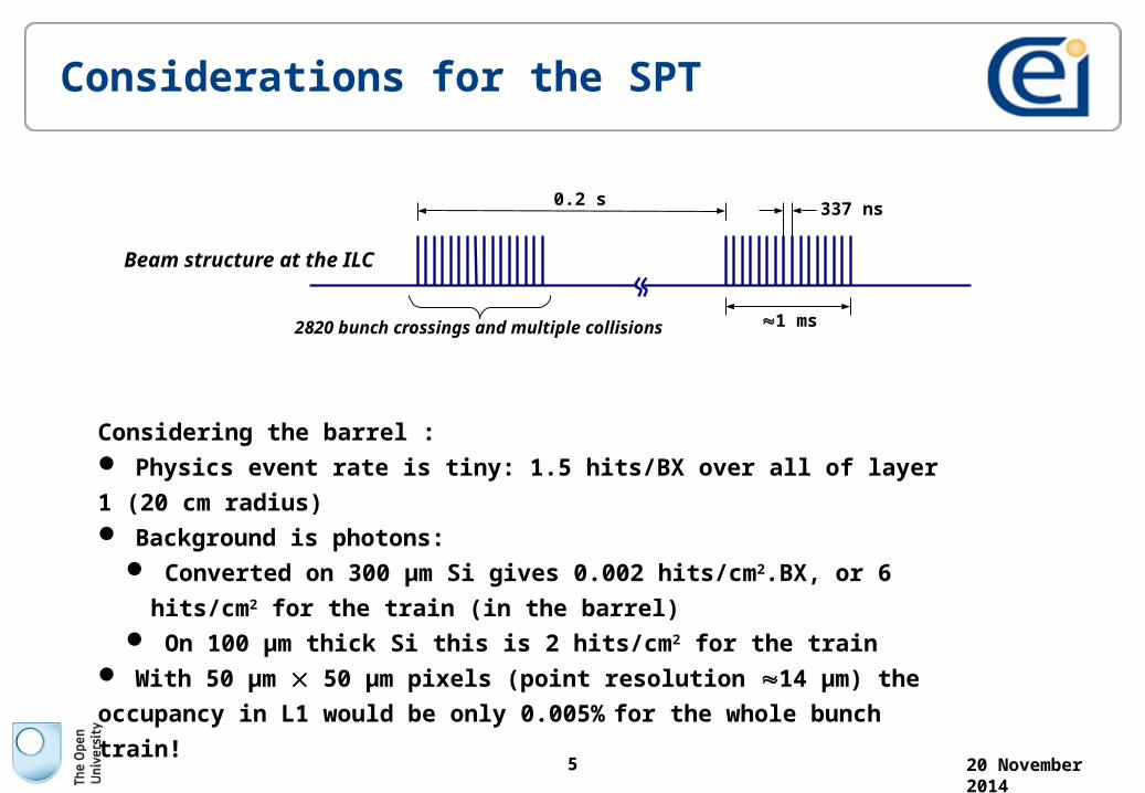
Considerations for the SPT
Considering the barrel : Physics event rate is tiny: 1.5 hits/BX over all of layer 1 (20 cm radius) Background is photons:
Converted on 300 μm Si gives 0.002 hits/cm2.BX, or 6 hits/cm2 for the
train (in the barrel) On 100 μm thick Si this is 2 hits/cm2 for the train
With 50 μm 50 μm pixels (point resolution 14 μm) the occupancy in L1
would be only 0.005% for the whole bunch train!
337 ns
0.2 s
1 ms
Beam structure at the ILC
2820 bunch crossings and multiple collisions

6 20 November 2014
The SPT Concept
Tracking sensor (one of 11,000), 8x8 cm2, 2.56 Mpixels each
Matching endcaps (only one shown)
• Barrels: SiC foam ladders
• Tracking layers: 5 cylinders, ~0.6% X0 per layer, 3.0% X0 total, over full polar angle
range ~50 mm square pixels
• Outer timing layers: ~3 cylinders as an envelope, ~2% X0 per layer if evaporative CO2
cooling ~150 mm square pixels
• Endcaps: 5 tracking and ~3 timing layers, closing off the nested barrels
• Tracking layers are read out between bunch trains (5 Hz or 50 Hz for ILC or CLIC)
Vertex detector
Timing layers
7 20 November 2014
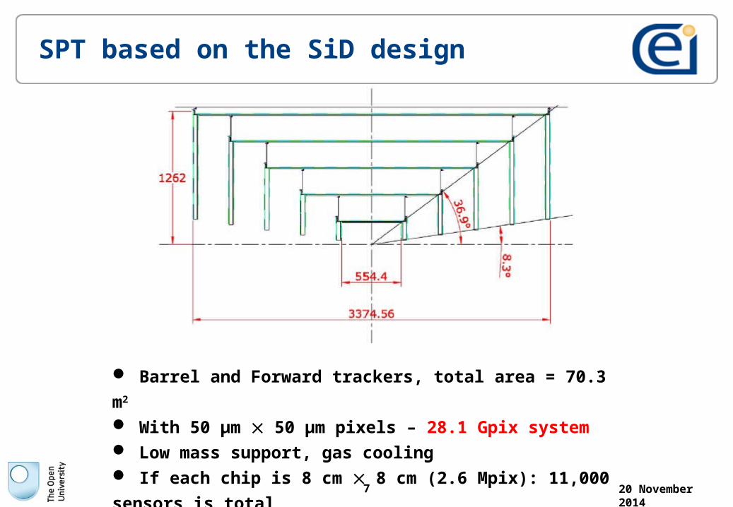
SPT based on the SiD design
Barrel and Forward trackers, total area = 70.3 m2
With 50 μm 50 μm pixels – 28.1 Gpix system Low mass support, gas cooling If each chip is 8 cm 8 cm (2.6 Mpix): 11,000 sensors is total

8 20 November 2014
Track Reconstruction
• Start with mini-vectors from on-time tracks found in the triplet of outer timing layers, together with an approximate IP constraint. 3 timing layers provide sufficient redundancy
• Work inwards through each successive tracking layer, refining the track parameters as points are added
• Fine granularity (i.e. pixel systems) can to a great extent compensate for coarse timing. Precision time stamping costs power, hence layer thickness
• ‘Special methods’ are envisaged for low momentum tracks, K-shorts, lambdas and photon conversions
• Final track refinement, recovery of tiny inefficiencies, achieved by correlation with tracks found in the inner timing layers (the vertex detector)
• A detailed feasibility study is badly needed
9 20 November 2014
Detector Parameters
The main challenge is to reduce material and therefore power must be reduced Sensors 100 μm thick, low mass support (<1% X0 per layer in the SiD design) Gas cooled, power dissipation ~O(100 W), in SiD < 500 W Pixel size around 50 μm 50 μm (point resolution 14 μm in binary mode) Bunch stamping/time slicing tracker:
• Implies on-pixel intelligence and therefore more power• Binary readout and sparsification most likely, but measurement of charge centroid is
not excluded Integrating:
• Lowest power (due to slow readout) and low mass• Full pixel readout to local readout chip• Resolution likely to improve below 14 μm due to the use of charge centroid• Preferred if track reconstruction is fully efficient

10 20 November 2014
Detector Options
CMOS Active Pixel Sensors– Can do all 3 readout schemes: integrating, time slicing, bunch stamping (relevant
experience with CALICE)• Challenges:
– Large, low power pixels not easy (pinned photodiode not developed for large pixels)– Full depletion for fast charge collection
• Large, wafer scale devices have been demonstrated• 4T/5T examples: 4 e- noise at 5 MHz readout (7 µm pixels, 10µm depleted)
CCDs• Can work as an integrating tracker layer• Large devices available• Large pixels are easy, little to no R&D required
11 20 November 2014
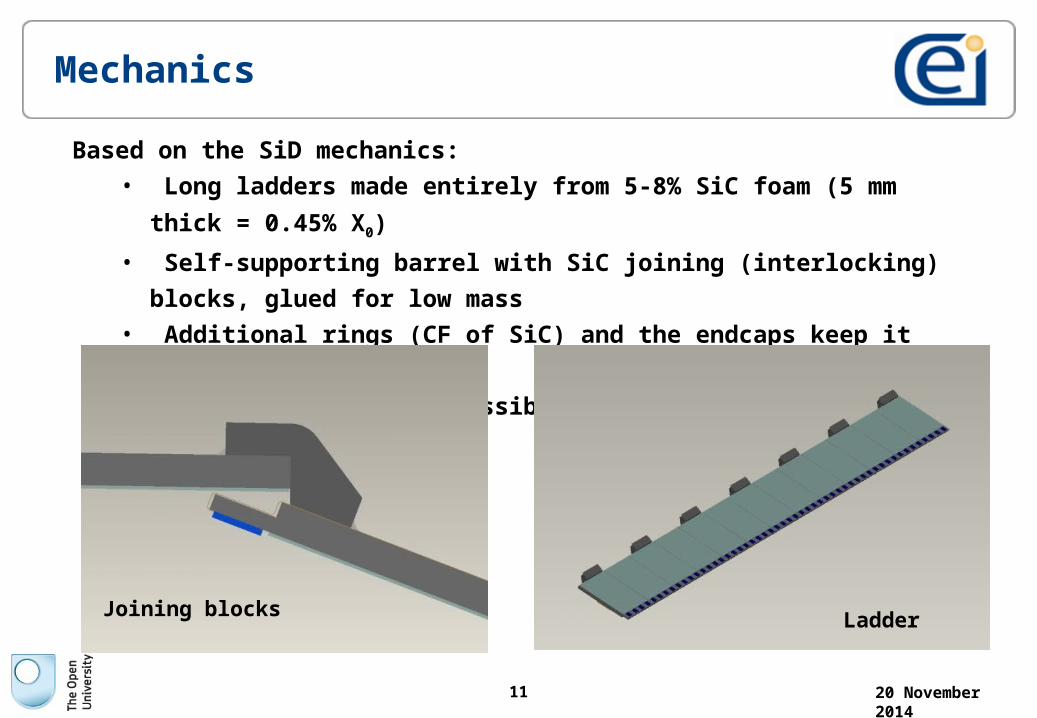
Mechanics
Based on the SiD mechanics:
• Long ladders made entirely from 5-8% SiC foam (5 mm thick = 0.45% X0)
• Self-supporting barrel with SiC joining (interlocking) blocks, glued for low mass• Additional rings (CF of SiC) and the endcaps keep it stable• This is one of many possible implementations…
Joining blocks Ladder

12 20 November 2014
Deformations - simulated
• Continuous foam cylinder
• Max deflection 10 mm
Steve Watson - RAL
• Separate foam ladders• Max deflection 20.5 mm
• Ladders joined by small foam piece every 40 cm
• Max deflection 20 mm

13 20 November 2014
Mechanics – more detailed look
Sensors: active width 8 cm, ~2 mm overlaps in r , fthickness ~60 mm, 30 mm active epi layer
Thin Cu/kapton tab (flexible for stress relief), wire bonds to sensor
Wedge links at ~40 cm intervals, each ~1 cm in length
** Cu/kapton stripline runs length of ladder, plus tabs (~5 mm wide) which contact each sensor
• Sparsified data transmitted on demand out of each detector (LVDS and optical fibres per end), continuously between bunch trains
• Continuous (not pulsed) power for tracking layers, hence minimising cross-section of power lines
• Tracking layers cooled by a gentle flow of nitrogen or air, hence no cooling pipes within tracking volume
• Outer timing layers need pulsed power, and probably evaporative CO2 cooling, to provide single-bunch readout
**
Devices will be 2-side buttable, so inactive regions in z will be ~ 200 mm (0.2%)
Adhesive-bonded non-demountable structure is not unheard of - SLD, astronomy
SiC foam, ~5% of solid density

14 20 November 2014
Forward Tracking
Mass of cables, connectors and cooling adds up heavily in the forward region Pulsed power (microstrips; time slicing or bunch stamping MAPS)
• Local energy storage (i.e. mass)• Cables rated for the peak power (i.e. mass again)
Cut-out view without endcaps
Continuous LOW power (integrating MAPS or CCDs)• Thin cables and no energy storage – lowest
mass possible• Just one cable per layer?

15 20 November 2014
Conclusions
• Silicon Pixel Tracker for the ILC is very attractive:– Low mass enabled by low power dissipation– Increased performance in the forward region– A combination of bunch stamping and integrating pixel layers – “separated function”
• Challenges:– Pattern recognition with different degrees of integration to be proven– Detector technology giving the required power dissipation, pixel size, noise, charge
collection time and sparsification algorithms– Mechanical support structure
• Opportunities: – Excellent tracking performance, both barrel and forward– Good science to be extracted– International leadership by UK institutions