a skin-like two-dimensionally pixelized full-color quantum dot … · quantum dot photodetector...
TRANSCRIPT

SC I ENCE ADVANCES | R E S EARCH ART I C L E
MATER IALS SC I ENCE
1Displays and Devices Research Lab. School of Electrical and Electronics Engineering,Chung-AngUniversity, Seoul 06974, Korea. 2Department of Chemistry, Chung-AngUni-versity, Seoul 06974, Korea. 3School of Advanced Materials Science and Engineering,SungkyunkwanUniversity, Suwon 16419, Korea. 4Division of Nano and Energy Conver-gence Research, Daegu Gyeongbuk Institute of Science and Technology (DGIST), 333,Techno Jungang Daero, Hyeonpung-Myeon, Dalseong-Gun, Daegu 42988, Korea.5Hyundai Motor Group R&D Division, Hwaseong-si, 18280, Korea. 6Department ofChemistry and the Materials Research Center, Northwestern University, 2145 SheridanRoad, Evanston, IL 60208, USA. 7Flexterra Corporation, 8025 Lamon Avenue, Skokie, IL60077, USA.*Corresponding author. Email: [email protected] (S.K.P.); [email protected] (M.-G.K.)
Kim et al., Sci. Adv. 2019;5 : eaax8801 22 November 2019
Copyright © 2019
The Authors, some
rights reserved;
exclusive licensee
American Association
for the Advancement
of Science. No claim to
originalU.S. Government
Works. Distributed
under a Creative
Commons Attribution
NonCommercial
License 4.0 (CC BY-NC).
Dow
nload
A skin-like two-dimensionally pixelized full-colorquantum dot photodetectorJaehyun Kim1, Sung-Min Kwon1, Yeo Kyung Kang2, Yong-Hoon Kim3, Myung-Jae Lee4,Kwangjoon Han5, Antonio Facchetti6,7, Myung-Gil Kim3*, Sung Kyu Park1*
Direct full-color photodetectors without sophisticated color filters and interferometric optics have attractedconsiderable attention for widespread applications. However, difficulties of combining various multispectral semi-conductors and improving photon transfer efficiency for high-performance optoelectronic devices have impededthe translation of these platforms into practical realization. Here, we report a low-temperature (<150°C) fabricatedtwo-dimensionally pixelized full-color photodetector by using monolithic integration of various-sized colloidalquantum dots (QDs) and amorphous indium-gallium-zinc-oxide semiconductors. By introducing trap-reduced che-lating chalcometallate ligands, highly efficient charge carrier transport and photoresistor-free fine-patterning ofQD layers were successfully realized, exhibiting extremely high photodetectivity (>4.2 × 10¹⁷ Jones) and photo-responsivity (>8.3 × 10³ A W−1) in a broad range of wavelengths (365 to 1310 nm). On the basis of these tech-nologies, a wavelength discriminable phototransistor circuit array (>600 phototransistors) was implemented on askin-like soft platform, which is expected to be a versatile and scalable approach for wide spectral image sensorsand human-oriented biological devices.
ed
on March 31, 2020http://advances.sciencem
ag.org/from
INTRODUCTIONAn integrated full-color [ultraviolet (UV)–to–infrared (IR)] photo-detector fabricated on a skin-like soft platform may offer the collectionof meaningful information from a body and the surroundingenvironment, enabling forthcoming human-oriented technologies suchas neuromorphic image sensors (1), soft robotics (2), and biologicalhealth monitoring (3). In addition, when addressing complex monitor-ing targets and environmental conditions, two-dimensional full-colorphotodetection on a single platformmay have a considerable advantagecompared to single- or narrow-band photodetection for target discrim-ination and acquisition of more reliable and extensive information (4).Conventional and recently reported photodetection systems, however,are mostly composed of a simple combination of individual photode-tectors, which can only detect a specific or limited range of wavelength,resulting in low pixel resolution, limited tunability of bandwidth, and acomplex device architecture (5). In addition, the difficulty of integratinghigh-resolution multilayered photosensing materials and device arraysfor full-color range photodetection with monolithic integration hasbeen a serious impediment for the realization of highly responsiveand full-color discriminable skin-like photodetectors arrays (6).
For these reasons, there have been enormous efforts to developphotodetectors with new photosensing materials and device architec-tures for broadband photodetection, such as colloidal quantum dots(QDs) (7), amorphous oxide semiconductors (AOSs) (8), organic semi-conductors (9), perovskite materials (10), and two-dimensionalmaterials (graphene and transition metal dichalcogenides) (11). In par-ticular, for maximizing the photosensitivity in a broadband range,
hybrid device architectures of photodetectors have been largely pursued(12, 13). For example, graphene-QDs (4), MoS2-graphene (14), AOSs-QDs (15), and organic-carbon nanotube photodetectors (16) have beenreported, demonstrating high gains and optical sensitivities as a result ofcombining semiconductors with distinct optoelectronic and chargetransport properties. However, although the previous advances arenoteworthy, they typically presented a narrow-band absorbingmaterialwith limited bandgap tunability and wavelength-discriminating ability(17). To overcome these limitations, particularly in terms of photo-sensitivity, full-color photodetection, and wavelength discrimination,colloidal QDs have attracted considerable attention for their unique op-toelectronic characteristics such as a wide bandgap tunability and highlight absorption coefficients (18, 19). In addition, for large-area andactive-matrix driving of the photodetectors, AOSs such as amorphousindium-gallium-zinc-oxide (a-IGZO)–based thin-film transistors(TFTs) have been actively investigated owing to their high carrier mo-bility, low off-state current, and scalability (20). Despite the interestingproprieties of colloidal QDs and a-IGZO, their monolithic integrationfor highly sensitive full-color photodetection has been rarely reported,mainly due to several issues (15, 17), particularly (i) the optimization ofQD/a-IGZO photodetector architecture for full-color photodetectionand wavelength discrimination, (ii) the realization of a complementarymetal-oxide semiconductor (CMOS)–compatible high-resolutionpatterning of multi-QD layers for a large-area and skin-like multiplex-ing array, and (iii) the poor control of the QD/a-IGZO interface toachieve a highly efficient charge transfer.
Here, we report a versatile and large-area scalable approach to ex-tend the detection bandwidth of a photodetector from UV to IR, usingmonolithic integration of QDs with a-IGZO phototransistors and im-plementing a low-temperature fabricated two-dimensional in-pixelcharge integrating circuit (CIC) array for color discrimination. In par-ticular, by introducing an electrically high-performance and trap-reduced chelating chalcometallate ligand for the QDs, ultrahighphotodetectivity (4.2 × 10¹⁷ Jones) was achieved, which is a record inthe best solution-processed organic andQDdevices so far. In addition, ahigh-resolution patterning of multiple QD layers via a direct photopat-terning and their pixelized phototransistors are demonstrated for a
1 of 12

SC I ENCE ADVANCES | R E S EARCH ART I C L E
skin-like two-dimensional photodetector that is capable of position-dependent full-color photodetection.
RESULTS AND DISCUSSIONDevice structure and operation mechanismTo realize full-color photodetection with high sensitivity, two strategieshave been carried out; first, the photodetector architecture and the in-pixel circuit were designed for high sensitivity, and second, monolithicintegration of QDs with an a-IGZO active layer and interfacial controlfor full-color light absorption and highly efficient charge collectionwereoptimized. Recently, three-terminal photodetector devices such as aphototransistor have been extensively investigated since they out-perform the conventional photodiodes in terms of photosensitivity, ex-ternal quantum efficiency (EQE), and a sublinear responsivity to
Kim et al., Sci. Adv. 2019;5 : eaax8801 22 November 2019
irradiance, especially at low intensities (13, 21). Therefore, the highphoto-sensitivity and the sublinear responsivity of the phototransistors enable awide dynamic range operation, particularly when arrayed with pixelizedschemes for image sensors and two-dimensional large-area applications.Figure 1A shows the schematic device and array structures of a flexibleQD/a-IGZOphotodetector fabricatedonanultrathinpolyimide (PI) sub-strate (see the Supplementary Materials for detailed fabricationprocedure). The cross-sectional high-resolution transmission electronmicroscope (HRTEM) images confirm the stacking of QDs on thea-IGZO layer and also the uniform distribution of the QD layer(Fig. 1, D to F). For detection of the light for full-color range, variousQD layers having different bandgaps, particularly PbS QDs (10 nmdiameter; bandgap, 0.95 eV), CdSe QDs (7 and 5 nm diameter; band-gaps, 1.95 and 2.39 eV, respectively), and CdS QDs (3 nm diameter;bandgap, 3.07 eV), were separately formed on the a-IGZO layer in a
on March 31, 2020
http://advances.sciencemag.org/
Dow
nloaded from
Fig. 1. Schematic of the device structure of the QD/AOS hybrid phototransistor. (A) A schematic three-dimensional view of a phototransistor array. (B) Optical ab-sorption of QDs used to fabricate the full-color detectors. (C) PbS QDs (10 nm diameter), CdSe QDs (7 nm diameter), CdSe QDs (5 nm diameter), and CdS QDs (3 nmdiameter) absorb IR, red, green, and blue, respectively. (D) Three-dimensional impression image of phototransistor and (E and F) corresponding cross-sectional HRTEMimages. Scale bars, 50 nm (E) and 5 nm (F). a.u., arbitrary units. Photo credit: Jaehyun Kim, Displays and Devices Research Lab. School of Electrical and ElectronicsEngineering, Chung-Ang University, Seoul 06974, Korea.
2 of 12

SC I ENCE ADVANCES | R E S EARCH ART I C L E
on March 31, 2020
http://advances.sciencemag.org/
Dow
nloaded from
pixelized manner (Fig. 1C and fig. S1). Although the semiconductingQDs have been integrated in several optoelectronic devices, includingTFTs, because of their inherent tunable bandgaps and high/broad lightabsorption (Fig. 1B), charge transport is frequently limited by the lig-ands connecting the QDs (22). On the other hand, a-IGZO TFTs ex-hibit high electronmobilities (fig. S2), but their photonic performanceis limited by low absorption property outside the UV region (fig. S3)(20, 23). However, the synergetic QDs with a-IGZO implementationin the TFT channel, combining a good light absorber that efficientlygenerates transport electron-hole pairs and a high mobility layer, en-able a scalable and high-performance full-color photodetecting devicefunctioning wavelength discrimination from UV to IR light.
Furthermore, the surface structure of QDs, particularly the ligands,strongly affects the charge transfer efficiency of the photogenerated car-riers at the QD/a-IGZO interface (22). However, typical QDs have longinsulating alkyl chains such as oleic acid as ligands, which substantiallyimpede the charge transfer between the QDs and the a-IGZO film.Thus, to enhance the charge transfer efficiency, a ligand exchange toshort and conducting ligands such as ethanedithiol (24), thiocyanate(SCN−) (25), and atomic ligands (26) has been investigated (fig. S4).In addition, there are various chalcometallate ligands for QDs, suchas Sn2S6
4−, Sn2Se64−, In2Se4
2−, Cu7S4−, Sb2S4
2−, Sb2Se42−, and CdQ2
2−
(Q = Se, Te) to cite a few of them (27). In this study, the critical require-ments for ligand choice are stable shell formation and facile electrontransport. Considering the stability, accessibility, and sufficient electrontransport, we have chosen Sn2S6
4− as the ideal system among variouschalcometallate ligands (28). Furthermore, since SCN− ligand–basedQDs have been widely investigated in high-conductivity/mobilityelectronic devices, we chose this ligand as the reference in our study.Here, in the case of SCN−-capped QDs, easy decomposition of ligandsdue to weak monodentate binding results in the formation of sulfur va-cancies on the QD surface. These sulfur vacancies can then act ascharge-trapping sites, preventing an efficient charge transfer betweenthe QDs and the a-IGZO channel layer. On the other hand, the biden-date Sn2S6
4− ligands minimize the generation of sulfur vacancies on theQD surface. Overall, the photogenerated electrons from the Sn2S6
4−-capped QDs can be efficiently transferred into the conduction band ofthe a-IGZO channel layer for charge collection, with minimal trappingevents (fig. S5). Also, the photogenerated holes remain in theQDs or nearthe QD/a-IGZO interface due to the large energy barrier between thevalence band maximum of QDs and a-IGZO.
Interfacial properties of QD/a-IGZOphototransistor performanceThe optical response characteristics of QD/a-IGZO phototransistorswere investigated by using various spectroscopic analyses, such as inter-facial trap-relatednoise analysis and scanningphotocurrentmicroscopy(SPCM). Figure 2 (A and B) shows the noise power spectral density(Sv) of SCN
− and Sn2S64− ligand–capped CdSe QD (7 nm diameter)/
a-IGZOphototransistors. According to the interface trappingmodel forthe flicker noise (1/f ) analysis, the Sv can be expressed as (29)
Sv ¼ ðq2=Cox2Þ⋅ðVD
2=ðVG � VthÞ2Þ⋅ ðkT DtÞ=ðLW lnðt1=t0ÞÞ⋅ð1=f Þðð1Þ
where q is the elementary charge,Cox is the gate oxide capacitance,VD isthe drain voltage,VG is the gate voltage,Vth is the threshold voltage, k isthe Boltzmann constant, T is the temperature, Dt is the interface trap
Kim et al., Sci. Adv. 2019;5 : eaax8801 22 November 2019
density, L is the length of the channel, W is the width of the channel,f is the frequency, and t0 and t1 are the minimum and maximum tun-neling time, respectively. Here, we assume that t1/t0 = 1012 to be con-sistent with previous work (29, 30), and from the results shown in Fig. 2(A and B),Dt is estimated as ~4.36 × 10¹⁵ and ~7.5 × 10¹² eV−1 cm−2 forSCN−- and Sn2S6
4−-cappedCdSeQD/a-IGZOphototransistors, respec-tively (at f= 10Hz). It is noted that the SCN−-cappedCdSeQD/a-IGZOphototransistor has ~103 times higher trap density than that of theSn2S6
4−-capped CdSe QD/a-IGZO phototransistor. In particular, theSn2S6
4−-capped CdSe QD/a-IGZO phototransistor has extremely lowtrap sites compared with previous works for silicon transistors (31).These results are consistent with the SPCM results, as shown in Fig. 2(C and D). Here, the total photocurrent and the optical reflectance aremeasured as a function of the laser position on the phototransistors(llaser = 532 nm, power = 0.45 mW, and beam spot size = 500 nm;figs. S6 and S7). The laser is scanned across the source, channel, anddrain regions, while measuring the current through the groundeddrain electrode. As shown in Fig. 2 (E and F), the Sn2S6
4−-capped CdSeQD/a-IGZO phototransistor exhibits a large Gaussian current profile,showing a photovoltaic-dominated process, while the SCN−-cappedCdSe QD/a-IGZO phototransistor shows a clear photothermoelectricresponse (32). In addition, we observed that the photocurrent level ofthe Sn2S6
4−-capped phototransistor is much higher than that of theSCN−-capped phototransistor, owing to the efficient transfer of photo-generated electrons from CdSe QDs to the a-IGZO layer, without anycharge carrier trapping problem. These results indicate that efficientelectron transfer from QDs to a-IGZO is crucial for achieving highphotoresponse characteristics.
Figure 3 (A and B) shows the transfer characteristics of SCN−- andSn2S6
4−-capped CdSe QD/a-IGZO phototransistors under differentlight intensities. Compared to the SCN−-capped phototransistors, theSn2S6
4−-capped phototransistors still exhibit low subthreshold slope(SS) and high mobility under light illumination. For instance, at a lightintensity of 1.36 mW cm−2, the Sn2S6
4−-capped phototransistorsshowed SS and mobility of 0.226 V decade−1 and 22.01 cm2 V−1 s−1,respectively, while the SCN−-capped phototransistors showed SS andmobility of 0.726 V decade−1 and 10.75 cm2 V−1 s−1, respectively. Sincethe degradation of SS under light illumination can be attributed to theformation of additional trap states, the lower SS value of Sn2S6
4−-cappedphototransistors indicates low level of trap states and, consequently,enhanced optoelectronic characteristics (fig. S8). Figure 3 (C and D)compares the photosensitivity (R) and photodetectivity (D*) of SCN−-and Sn2S6
4−-capped CdSe QD/a-IGZO phototransistors under the whitelight and broadband illumination (365, 406, 520, 638, and 1310 nm).Here, R and D* are evaluated by the following equations (13, 15)
R ¼ Iph=P; D� ¼ ðADf Þ1=2=NEP; NEP ¼ ðð⟨In2⟩Þ1=2=RÞ ð2Þ
where Iph is the photocurrent (Iph = Ilight − Idark), P is the light power, Ais the illuminated area, Df is the spectral bandwidth, NEP is the noiseequivalent power, and (⟨In
2⟩)1/2 is the root mean square dark noisecurrent from the noise power spectral density. The Sn2S6
4−-cappedCdSe QD/a-IGZO phototransistors exhibit extremely high R and D*values of ~8.3 × 10³ AW−1 and ~4.2 × 10¹⁷ Jones (white light inten-sity = 1.36mWcm−2), respectively, compared to those of SCN−-cappedphototransistors (R = ~3.1 × 10³ A W−1 and D* = ~5.7 × 10⁸ Jones).Also, Sn2S6
4− ligand–based devices showed D* values of ~1.9 × 10¹⁹,~1 × 10¹⁸, ~7.3 × 10¹⁷, ~3.6 × 10¹⁷, and ~1.3 × 10¹² Jones withUV, blue,
3 of 12

SC I ENCE ADVANCES | R E S EARCH ART I C L E
on March 31, 2020
http://advances.sciencemag.org/
Dow
nloaded from
green, red, and IR irradiation, respectively (fig. S9). These values areabout five to six orders of magnitude higher than previous work inthe UV range, about four orders of magnitude higher than previouswork in the visible range, and about one order ofmagnitude higher thanprevious work in the IR range when considering solution-processed or-ganic andQDdevices reported to date (17, 21, 33, 34). Here, the noise ofthe device is determined by flicker (1/f) noise, which is a resistance fluc-
Kim et al., Sci. Adv. 2019;5 : eaax8801 22 November 2019
tuation and always relates to a direct current to avoid overestimating thephotodetectivity (35). It is argued that such high photoresponse char-acteristics of Sn2S6
4−-capped phototransistors are attributed to the ex-tremely low 1/f noise (~10−34 A2 Hz−1) of the device and the highlyconducting and trap-reduced Sn2S6
4− ligands of our CdSe QDs. Fur-thermore, the Sn2S6
4−-capped phototransistors exhibit a considerablylow off-current level (10−13 to 10−14 A) and a high illuminated-current
Fig. 2. Interfacial properties betweenQDs and the AOS channel layer. (A and B) Noise power spectral density of 7-nm CdSe QD/a-IGZO with SCN− and Sn2S64− ligand
phototransistors. (C andD) Scanning photocurrent imaging (0 V source per drain bias) of the QD/a-IGZO phototransistor with Sn2S64− and SCN− ligands. Scale bars, 5 mm.
(E and F) Photocurrent profile with a laser wavelength of 532 nm and a power of 0.45 mW from along the blue dashed line in (C) and (D). Photo credit: Jaehyun Kim,Displays and Devices Research Lab. School of Electrical and Electronics Engineering, Chung-Ang University, Seoul 06974, Korea.
4 of 12

SC I ENCE ADVANCES | R E S EARCH ART I C L E
on March 31, 2020
http://advances.sciencemag.org/
Dow
nloaded from
level (~10−4 A), high EQE (Fig. 3E), wide dynamic range in a broadrange of gate bias (>150 dB at VGS = −10 to −2 V, Fig. 3F), and fastphotoresponse and decaying behavior (figs. S10). Compared to previousQD phototransistor studies (15, 36) reporting photoresponse timesfrom 0.6 to 0.3 s, our results demonstrate photoresponses of 0.27 s to90ms, which are at least three times smaller than those in the literature.Although the speed of our photodetectors remains affected by sometrapped charges at the QD interconnections as evidenced from the in-cident light power–dependent time response of our devices (figs. S11and S12), the Sn2S6
4−-QD/a-IGZO have shown amuch reduced photo-response time than others, which should be sufficient for photodetectorand image-sensing applications.
Kim et al., Sci. Adv. 2019;5 : eaax8801 22 November 2019
High-resolution patterning of QD layers usingdirect photopatterningAlthough the monolithic integration of QDs and AOS layers is pursuedto achieve high photoresponse characteristics, high-resolution patterningofQDmultiple layers for pixelation is also required to fabricate functionalphotodetector arrays that guarantee high photodetectivity and wide dy-namic range by reducing the leakage currents. Recently, various pat-terning techniques including inkjet printing, electron beam writing,and transfer printing have been explored for pixelation of QDs (37).However, several issues such as limited resolution, poor reliability overa large area, chemical contamination, and fabrication complexity are stillproblematic. Here, we used a CMOS-compatible direct photopatterning
Fig. 3. Optoelectronic performance of the QD/AOS hybrid phototransistor. Photoresponse characteristics of the QD/a-IGZO phototransistor with (A) Sn2S64− and (B) SCN−
ligands. (C) Photosensitivity (R) and (D) photodetectivity (D*) under white light (1.36mW cm−2) and broadband illumination (inset). Light intensities of UV, blue, green, and redare 1mWcm−2, while that for IR is 13.6mWcm−2 and that forwhite light is 1.36mWcm−2. (E) EQE and (F) dynamic rangeof 7-nmCdSeQD/a-IGZOwith the Sn2S6
4− ligand (blueline) and the SCN− ligand (red line) phototransistor. Photo credit: Jaehyun Kim, Displays andDevices Research Lab. School of Electrical and Electronics Engineering, Chung-AngUniversity, Seoul 06974, Korea.
5 of 12

SC I ENCE ADVANCES | R E S EARCH ART I C L E
Dow
nloaded from
process to achieve isolated QD layers for sensor arrays without anyphotoresist, using the high photochemical reactivity of Sn2S6
4− ligandsby UV exposure (fig. S13) such that a photolithography process forpixelation of QD layer is possible. As shown in Fig. 4A, the photo-chemical reaction of Sn2S6
4− results in the formation of a stableSnS2 shell (almost identical optoelectrical performance with Sn2S6
4−
ligands, fig. S14), rather than desorption or decomposition of the ligand,suppressing the formation of anion vacancies and subsequent genera-tion of electron-trapping states. As a result, the UV-exposed regionbecomes insoluble to dimethyl sulfoxide (DMSO)/ethanolamine (EA)mixed solvent, while the unexposed region remains soluble. In Fig. 4 (Bto G), field-enhanced scanning electron microscopy (FESEM) andatomic forcemicroscopy (AFM) images of patternedQD layers confirmthe clear patterning of QD layers, having a thickness of ~17 nm (two tothree layers of QDs; different types of patterned QDs are also shown infigs. S15 and S16). In addition, the UV-induced photochemical reactionof Sn2S6
4−-capped CdSe QDs is verified by the x-ray photoelectronspectroscopy (XPS) analysis. By the UV exposure, the Sn2S6
4−-cappedCdSe QDs exhibit a significant reduction in the normalized S2p peakover the Sn3d5/2 peak (from 0.304 to 0.163 after UV exposure), indicat-ing the formation of SnS2, which corresponds to the theoretical stoichi-ometry change from Sn2S6
4− into SnS2 (fig. S17). Overall, the directphotopatterning of QD layers can effectively reduce the number of
Kim et al., Sci. Adv. 2019;5 : eaax8801 22 November 2019
patterning steps and avoid any contact with the photoresist, preventingthe degradation caused by the impurity contamination.
Full-color photodetection using an in-pixel CICUsing the direct photopatterning of variousQD layers, a full-color (UV-to-IR) CIC was fabricated (Fig. 5A). Each pixelized QD layer had a pat-tern size of 40 mmby 100 mm, and the process was repeated to create fivedifferentmultilayer structures of red (R), green (G), blue (B), and IRQDlayers on a-IGZO and a bare a-IGZO for UV detection. The a-IGZOlayer is used as channel material for control/switch and wavelength-discriminating integrated circuits. With 600 QD/a-IGZO phototransis-tors (fig. S18), as shown in Fig. 5 (A and B), in-pixel CIC array isimplemented. The schematic of Fig. 5A includes four QD/a-IGZOwithSn2S6
4− ligand phototransistors [10-nm PbS (T1), 7-nm CdSe (T2),5-nm CdSe (T3), and 3-nm CdS (T4) QD/a-IGZO TFTs] for IR, R, G,and B detection and two pristine a-IGZO TFTs (T5 and T6; T5, outputTFT; T6, driver TFT) for in-pixel amplification circuit and UV detec-tion as well. In particular, the T5/T6 transistor not only enablesamplification (fig. S19) but also functions as a UV detector because ofthe high photoresponsivity of pristine a-IGZO to the UV region. In thedark, there is no transistor response and the lowest output currents cor-respond to a logic level of (T1 T2 T3 T4 T5; 0 0 0 0 0). Upon IR lightillumination, only the T1 transistor activates, resulting in a logic level of
on March 31, 2020
http://advances.sciencemag.org/
Fig. 4. Fine-patterned QDs characteristics. (A) Schematic representation of QDs to design photosensitive inorganic ligands. (B) Optical and (C) field-enhanced scanningelectron microscopy (FESEM) images of patterned CdSe QDs capped with Sn2S6
4− ligands. (D) CdS QDs, (E) PbS QDs. Scale bars, 100 mm (B), 5 mm (C), 20 mm (D), and 10 mm(E). (F andG) Atomic forcemicroscopy (AFM) scan image and height profile of CdSeQDs from along the blue dashed line. Scale bar, 5 mm. Photo credit: Jaehyun Kim, Displays andDevices Research Lab. School of Electrical and Electronics Engineering, Chung-Ang University, Seoul 06974, Korea.
6 of 12

SC I ENCE ADVANCES | R E S EARCH ART I C L E
(T1 T2 T3 T4 T5; 1 0 0 0 0). In the cases of red, green, and blue lightilluminations, the logic levels of the CIC are (1 1 0 0 0), (1 1 1 0 0),and (1 1 1 1 0), respectively. Upon UV illumination, all transistorsactivate due to the higher UV optical energy than the bandgapenergy of all QDs and a-IGZO; thus, the system exhibits a logic level
Kim et al., Sci. Adv. 2019;5 : eaax8801 22 November 2019
of (1 1 1 1 1) and the highest output current (Fig. 5, C to G). By intro-ducing the linear integration of the six phototransistors with a signal-amplification scheme (38), the output current level of the CIC can beassociated to a specific wavelength, allowing recognition of variouswavelengths of incident light as shown in Fig. 5H (whereas limitation
on March 31, 2020
http://advances.sciencemag.org/
Dow
nloaded from
Fig. 5. CIC array characteristics for full-color discrimination. (A) Schematic diagram of CIC and logic table of full-color signal detection in one pixel. (B) Optical micrograph ofthe partially patternedQDs including IR PbS (T1, 10 nm), redCdSe (T2, 7 nm), greenCdSe (T3, 5 nm), andblueCdS (T4, 3 nm) andbare a-IGZOphototransistors and the schematic ofamplification circuit. RTN is the channel resistance of load TFTs (T1 to T4), and RT6 is the channel resistance of driver TFT (T6). Here, channel width/length are 100/50 mm (load TFTs),200/10 mm(T5), and 5/200 mm(T6). Scale bar, 50 mm. (C toG) Photoresponse characteristics of T1, T2, T3, T4, and T5/T6with respect towavelength of light. (H) Output current of thefive-channel full-color photodetector. (I) Mixed light discrimination. Light intensities of UV, blue, green, and red are 1 mW cm−2, while that for IR is 13.6 mW cm−2. For yellow, red(0.5 mW cm−2) and green (0.5 mW cm−2) were mixed, and for cyan, green (0.5 mW cm−2) and blue (0.5 mW cm−2) were mixed. Photo credit: Jaehyun Kim, Displays and DevicesResearch Lab. School of Electrical and Electronics Engineering, Chung-Ang University, Seoul 06974, Korea.
7 of 12
SC I ENCE ADVANCES | R E S EARCH ART I C L E
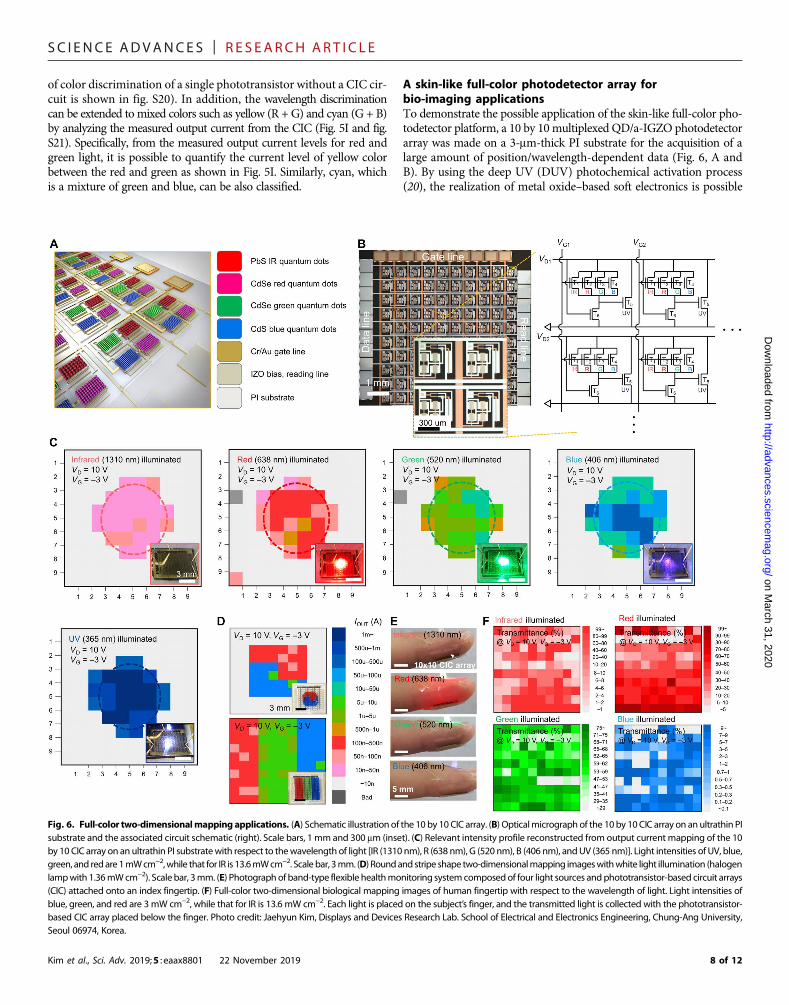
of color discrimination of a single phototransistor without a CIC cir-cuit is shown in fig. S20). In addition, the wavelength discriminationcan be extended to mixed colors such as yellow (R + G) and cyan (G + B)by analyzing the measured output current from the CIC (Fig. 5I and fig.S21). Specifically, from the measured output current levels for red andgreen light, it is possible to quantify the current level of yellow colorbetween the red and green as shown in Fig. 5I. Similarly, cyan, whichis a mixture of green and blue, can be also classified.
Kim et al., Sci. Adv. 2019;5 : eaax8801 22 November 2019
A skin-like full-color photodetector array forbio-imaging applicationsTo demonstrate the possible application of the skin-like full-color pho-todetector platform, a 10 by 10multiplexed QD/a-IGZO photodetectorarray was made on a 3-mm-thick PI substrate for the acquisition of alarge amount of position/wavelength-dependent data (Fig. 6, A andB). By using the deep UV (DUV) photochemical activation process(20), the realization of metal oxide–based soft electronics is possible
on March 31, 2020
http://advances.sciencemag.org/
Dow
nloaded from
Fig. 6. Full-color two-dimensionalmapping applications. (A) Schematic illustration of the 10 by 10 CIC array. (B) Opticalmicrograph of the 10 by 10CIC array on anultrathin PIsubstrate and the associated circuit schematic (right). Scale bars, 1 mm and 300 mm (inset). (C) Relevant intensity profile reconstructed from output current mapping of the 10by 10 CIC array on an ultrathin PI substratewith respect to thewavelength of light [IR (1310 nm), R (638 nm), G (520 nm), B (406 nm), andUV (365 nm)]. Light intensities of UV, blue,green, and redare1mWcm−2,while that for IR is 13.6mWcm−2. Scalebar, 3mm. (D) Roundand stripe shape two-dimensionalmapping imageswithwhite light illumination (halogenlampwith 1.36mWcm−2). Scale bar, 3mm. (E) Photographof band-type flexible healthmonitoring systemcomposedof four light sources andphototransistor-based circuit arrays(CIC) attached onto an index fingertip. (F) Full-color two-dimensional biological mapping images of human fingertip with respect to the wavelength of light. Light intensities ofblue, green, and red are 3 mW cm−2, while that for IR is 13.6 mW cm−2. Each light is placed on the subject’s finger, and the transmitted light is collected with the phototransistor-based CIC array placed below the finger. Photo credit: Jaehyun Kim, Displays and Devices Research Lab. School of Electrical and Electronics Engineering, Chung-Ang University,Seoul 06974, Korea.
8 of 12

SC I ENCE ADVANCES | R E S EARCH ART I C L E
on March 31, 2020
http://advances.sciencemag.org/
Dow
nloaded from
since theDUVphotochemical activation enables the formation of high-performance oxide semiconductors such as IGZO at a low temperature(<150°C). In addition with the low temperature–processed QDs withchalcometallate ligands using nontoxic organic solvents, a multiplexingphotodetecting array on an ultrathin PI substrate can be realized, whichcan be applicable in wearable health care monitoring devices such as anoxygen saturation measurement unit. Here, we observed no significantdifference in the photoresponse characteristics in those fabricated onglass and ultraflexible PI substrates (fig. S22). Figure 6C shows thetwo-dimensional areal mapping of output currents obtained from thephotodetector array under illumination of five different light sources(IR, R, G, B, andUV) (VG =−3V,VD=+10V). As shownhere, althoughseveral pixels in the outer region exhibit somewhat deviated currentranges, most of the pixels (yield >99%) show a spatially uniform currentdistribution to the corresponding light sources. Moreover, position-dependent color mapping is also possible by measuring the R/G/B lights,which are spatially separated from white light (round and strip shapes)(Fig. 6D). Furthermore, for biological applications, particularly for themonitoring of blood oxygen saturation level, the skin-like QD/a-IGZOphotodetector array was used to measure the absorption of variouswavelengths of light throughout the capillary blood vessels in theindex finger (Fig. 6E). The transmission of the light through the bloodvessel is varied by the organization of various components such as thebone and tissues, which absorb or scatter light differently. Also, thetransmission of the light varies depending on the absorptivity of deoxy-and oxy-hemoglobin in the red blood cells. Figure 6F shows the obtainedposition-dependent two-dimensionally mapped data for different lightsources, showing specific transmittance depending on the wavelength,which is well in agreement with previously reported data (39). The di-verse wavelength and position-dependent absorption data may lead to acritical advancement for more reliable and precise diagnostics in healthmonitoring systems in the near future.
Last, to verify the mechanical and environmental stability of theskin-like QD/a-IGZO photodetector, long-term lifetime and bending/cycling tests were carried out. By passivating the device with apoly(methyl methacrylate) (PMMA) layer having a thickness of~200 nm, the photosensitivity, photodetectivity, and the photo-current show only a small variation (<10%) even after 30 days of airexposure compared to the unpassivated devices (fig. S24). In addition,the photoresponse characteristics of the skin-like QD/a-IGZO photo-detector was stable under various bending (bending radius down to~150 mm) and cyclic conditions (0 to 1000 times), without showingany visiblemechanical cracks or damages and changes in optoelectronicperformances (figs. S25 to S28).
CONCLUSIONIn summary, the results presented here argue that low-temperature fab-ricated diverseQD-based phototransistors and their in-pixel CIC arraysoutperform conventional photodiode-based CMOS sensors and cur-rent state-of-the art flexible photodetectors, providing full-color photo-detection from UV to IR and thereby a general route for highly reliableand conformal two-dimensional photodetectors. The proven synergy ofmonolithic integration of QDs and AOS phototransistor systems withwavelength discrimination ability can also open new prospect of photo-detecting devices and electronics. Photosensitive and high-conductivechelating chalcometallate ligands can perfectly transfer photogeneratedelectrons to an AOS active layer without electron trapping, resulting inextremely high photosensitivity and photodetectivity. Furthermore,
Kim et al., Sci. Adv. 2019;5 : eaax8801 22 November 2019
these platforms can be applied to multichannel photosensor arraysdue to direct patterning of multiply pixelized QD layers to respond tovarious stimuli simultaneously and selectively, showing a facile route forvarious bio-imaging applications.
MATERIALS AND METHODSPreparation of QDs and chalcometallate ligandsReagentsLead acetate trihydrate [Pb(CH3COO)2∙3H2O,≥99.5%], bis(trimethylsilyl)sulfide [(CH3)3SiSSi(CH3)3], sodium sulfide nonahydrate (Na2S∙9H2O,≥98.0%), tin(IV) chloride pentahydrate (SnCl4∙5H2O, 98%), oleic acid[CH3(CH2)7CH═CH(CH2)7COOH, 90%], methylammonium chloride(CH3NH3Cl, 98%), and 1-octadecene [ODE; CH3(CH2)15CH═CH2,90%] were purchased from Sigma-Aldrich. Ethanol (C2H5OH,99.5%), methanol (CH3OH, 99.8%), acetone (CH3COCH3, 99%), andn-hexane (C6H14, ≥99%) were purchased from Daejung. CdSe QDs(5 and 7nm) andCdSQDs (3 nm) in hexane (20mg/ml)were purchasedfrom Uniam. All reagents were used without further purification.Ten-nanometer PbS QDsIn a synthesis of PbS QDs, 2 mmol lead acetate trihydrate was mixedwith 8 ml of oleic acid and 12 ml of ODE mixture in a 250-ml three-neck flask connected to a Schlenk line. To remove water and volatileimpurities, the mixture was heated at 100°C for 2 hours under vacuum.The whole mixture was further heated to 170°C. Separately, an S sourcesolutionwas prepared by dissolving 1mmol of bis(trimethylsilyl) sulfidein 10 ml of ODE. The S precursor solution was swiftly injected into theabove hot mixture, and the reaction was terminated immediately by re-moving the flask from the heating mantle. The reaction mixture wasnaturally cooled down to room temperature. After adding 90ml of hex-ane to the reaction mixture, 180 ml of ethanol was added into the so-lution and centrifuged at 10,000 rpm for 60 min. The colorlesssupernatant was discarded and the bottom QD precipitate was redis-persed in hexane. The process was repeated four times.(CH3NH3)4Sn2S6Na4Sn2S6∙14H2O (2.325mmol) andCH3NH3Cl (34.31mmol)were dis-solved in 3 ml of deionized water at room temperature. The solutionwas stirred at room temperature for 1 hour. The white precipitatewas washed with 40 ml of methanol four times. The product was driedunder vacuum at room temperature for 1 hour.
Ligand exchange for Sn2S64−-capped QDs
All of the ligand exchange processes were performed in a nitrogen-filledglove box with anhydrous solvents. Five milligrams of chleating chalco-metallate capping ligands, such as (CH3NH3)4Sn2S6, was dissolved in3 ml of the DMSO (99.8%, Sigma-Aldrich)/EA (99.5%, Sigma Aldrich)mixture (2:1 by volume). The solution was added into 2 ml of the oleicacid–capped QDs solution in hexane. After stirring for 3 to 4 hours, theupper colorless hexane part was carefully removed, and the solutionwasfurther washed with 2 ml of hexane several times. The ligand exchangeQDs solution was mixed with 9 ml of acetonitrile (99.8%, Sigma-Aldrich) and centrifuged at 5000 rpm for 5 min. The upper solutionwas discarded and the bottompart was redispersed inDMSO/EAmix-ture solution.
Ligand exchange for SCN−-capped QDsFive milligrams of ammonium thiocyanate (NH4SCN, 99.99%, Sigma-Aldrich) was dissolved in 1 ml of acetone, and the solution was addedinto 1ml of oleic acid–cappedQDs solution in hexane. After stirring for
9 of 12

SC I ENCE ADVANCES | R E S EARCH ART I C L E
on March 31, 2020
http://advances.sciencemag.org/
Dow
nloaded from
3 to 4 hours, the upper colorless hexane part was carefully removed, andthe solution was mixed with 1 ml of tetrahydrofuran (Sigma-Aldrich)and centrifuged at 3000 rpm for 2 min. The upper solution was dis-carded and the bottom part was redispersed in 1ml of toluene and cen-trifuged at 3000 rpm for 2 min. The upper solution was discarded andthe bottom part was dispersed in DMSO/EA mixture solution.
Phototransistor device fabricationPI (15 weight %, Picomax) varnish solution was spin-coated on a glasscarrier substrate and annealed at 300°C for 60min. ThePI substrate filmhad a nominal thickness of 3 mm(measured by a surface profiler). Here,glass substrate was used in the case of glass-based devices. Then, aCr/Au (5/45 nm) gate electrode was deposited by the evaporatorand patterned by using conventional photolithography. On the gateelectrode, a 50-nm-thick Al2O3 gate insulator layer was deposited usingthe atomic layer deposition system at 150°C, and IGZO [indium(III)nitrate hydrate (In(NO3)3∙x(H2O), 0.085 M), gallium(III) nitrate hy-drate (Ga(NO3)3∙x(H2O), 0.0125 M] and zinc acetate dihydrate[Zn(CH3COO)2∙2(H2O), 0.0275 M] (all purchased from Sigma-Aldrich) were dissolved in 2-methoxyethanol (anhydrous, 99.8%,Sigma-Aldrich) and stirred formore than12 hours at 75°C.The channellayer was spin-coated and photochemical activation was followed for2 hours in a N2 atmosphere using DUV light (Filgen, UV253H, 18 to23 mW cm−2). The a-IGZO channel layer and the Al2O3 gate insulatorlayer were patterned using photolithography. Then, a highly conductiveindium zinc oxide source/drain with a thickness of 100 nm wasdeposited using radio-frequency sputtering and patterned using thelift-off process. In addition, the QD layer was spin-coated on top ofa-IGZO TFTs and patterned using the direct optical lithographymethod, followed by annealing at 150°C for 20 min.
Patterning of the QD layerThe QD patterning process was carried out in a clean room via directoptical irradiation with a halogen lamp for 3 min with a quartz photo-mask. Radiant power is 50Wandbeamwavelength is 365 nm (OSRAMHBO350W/S). TheUV-unirradiated region of theQD layerwas rinsedout by DMSO/EA mixture solution so that only the UV-irradiatedregion remained.
Photoelectronic performance of phototransistorsAll electrical and photoresponse characteristics of QD/a-IGZO de-vices were carried out using Agilent 4156C (Agilent Co.) in air am-bient atmosphere at room temperature. For the light source, a whitelight source (halogen lamp, OSRAM, 64637, 100W) and a laser sourcewith wavelength centered at 1310-nm (IR), 638-nm (R), 520-nm (G),406-nm (B) (Thorlabs Co.), and 365-nm (UV) light-emitting diode(LED) were used. The power of white light was measured using a Siphotodiode detector (BS-520, S/N 130, Bunkoukeiki Co. Ltd.) andlaser/LED were measured using PM100A (Thorlabs Co.). To calcu-late photosensitivity (R) and the photodetectivity (D*), the followingequations were used (15)
R ¼ Iph=P; D� ¼ ðADf Þ1=2=NEP
where Iph is the photocurrent (Iph = Ilight − Idark), P is the light power,Ais the illuminated area (channel W × L), Df is the spectral bandwidth,and NEP is the noise equivalent power. Here, R was extracted from thephotoresponse transfer characteristics of the QD/a-IGZO photo-
Kim et al., Sci. Adv. 2019;5 : eaax8801 22 November 2019
transistor, and D* was evaluated using a root mean square dark noisecurrent of (⟨In
2⟩)1/2 from the noise power spectral density measured byusing a noise current preamplifier and a vector-signal analyzer. Also,NEP= ((⟨In
2⟩)1/2/R) can be calculatedwithR ofQD/a-IGZOphototran-sistors at different wavelengths, from the UV to the NIR wavelengthregion. The frequency/light intensity–dependent D* was calculated byanalyzing the dark noise current in the conducting channel withcorresponding optical modulated frequency. Also, EQE was extractedfrom the following equation (40)
R ¼ ðle=hcÞ � EQE� G
where R is the photosensitivity, l is the wavelength, e is the elementarycharge, h is the Planck constant, c is the speed of light, and G is thephotoconductive gain, which is given by the ratio of carrier lifetime(tlifetime) over the transit time (ttransit). Furthermore, ttransit = L2/mVDS,where L is the channel length, m is the carrier mobility, and VDS is thedrain-source voltage. Last, dynamic range was expected from the follow-ing definition (21)
Dynamic range ¼ ð20 log ðIlight=IdarkÞÞ
where Ilight is the drain current with the light illumination and Idark is thedrain current with the dark condition.
SPCM and interfacial trap-related noise analysisThe SPCM was carried out at room temperature in a confocal micro-scope setup with an objective with a numerical aperture of 0.8. The ex-citation was provided by a focused laser of a given wavelength (532 nm)and by a supercontinuum white light source (Fianium Ltd) combinedwith a monochromator for the high-resolution spectra (450 nm ≤ l ≤2000 nm) where l is the wavelength. During the wavelength scanning,photocurrent is measured by a lock-in technique with a chopper fre-quency of 500 Hz and subsequently normalized to the photon flux.The chopped laser beam is focused by a microscopic lens (numericalaperture, 0.8) and illuminates the QD/a-IGZO channel and S/Delectrode region of devices (32). For the noise measurement, the noisepower spectral densities were measured with an SR 570 low–noise cur-rent preamplifier (Stanford Research System, Sunnyvale, CA, USA) andan Agilent 35670A dynamic signal analyzer (Agilent Co.).
Characterizationsz-Potential measurementThe data were collected using Otsuka ELSZ-1000 (Otsuka Electron-ics, Japan). Colloidal QD solutions were filled into a quartz cuvetteusing a flow cell. The measurement was performed without airbubble in the cell.Fourier transform IR spectroscopyFourier transform IR spectra were obtained in the transmission modeusing Nicolet 6700 (Thermo Fisher Scientific). The QD films werecoated on the intrinsic Si wafer.X-ray photoelectron spectroscopyXPS was analyzed with a K-alpha XPS system (ThermoVG Scientific)using a monochromatic Al Ka source at 1486.6 eV and a base pressureof 7.83 × 10⁻⁹ mbar.Absorption spectraUV-visible–near IR spectroscopy (Cary 5000, Agilent) was used to eval-uate the light absorbance of a QD, an a-IGZO film, and a PMMA layer.
10 of 12

SC I ENCE ADVANCES | R E S EARCH ART I C L E
Nanostructures of the filmsNoncontact AFM (NX10, Park-systems), optical microscopy (BX53M,Olympus), FESEM (SIGMA, Carl Zeiss Co.), and HRTEM (Titan, FEI)were used. The samples were prepared by a Helios 650 (NanoLab)focused ion beam.
on Mhttp://advances.sciencem
ag.org/D
ownloaded from
SUPPLEMENTARY MATERIALSSupplementary material for this article is available at http://advances.sciencemag.org/cgi/content/full/5/11/eaax8801/DC1Fig. S1. Colloidal QD solutions.Fig. S2. Electrical characteristics of low-temperature photoactivated sol-gel a-IGZO TFTs.Fig. S3. Absorption spectra of a-IGZO film.Fig. S4. Synthesis and chemical analysis for chelating chalcometallate ligands (Sn2S6
4−).Fig. S5. Optoelectronic mechanism of a QD phototransistor.Fig. S6. SPCM analysis for a QD phototransistor.Fig. S7. SPCM analysis for an a-IGZO phototransistor.Fig. S8. Optoelectrical characteristics of a-IGZO TFT and oleic acid-QD/a-IGZO phototransistors.Fig. S9. Photodetectivity (D*) of a QD/a-IGZO phototransistor with Sn2S6
4− and SCN− ligands asa function of the frequency.Fig. S10. Photoswitching properties of CdSe QD/a-IGZO phototransistors.Fig. S11. Temporal response of CdSe QD/a-IGZO phototransistors.Fig. S12. Temporal photocurrent response of CdSe QD/a-IGZO phototransistors.Fig. S13. Absorption spectra of chelating chalcometallate ligands.Fig. S14. Optoelectrical characteristics of CdSe QD/a-IGZO phototransistors before and afterQDs patterning.Fig. S15. Examples of optically patterned QDs.Fig. S16. HRTEM images of the QDs.Fig. S17. XPS analysis of CdSe QDs.Fig. S18. Schematic of direct photolithography process for fine-patterned diverse QD layers.Fig. S19. In-pixel charge integrating and amplification circuit analysis.Fig. S20. Limitation of color discrimination of a single phototransistor without a CIC circuit.Fig. S21. Discrimination of various light wavelength from mixed light.Fig. S22. Five-channel QD/a-IGZO phototransistors composed of CIC pixel with glass and PIsubstrate.Fig. S23. Full-color two-dimensional biological mapping images.Fig. S24. Long-term reliability test for CdSe QD/a-IGZO with a Sn2S6
4− ligand phototransistor.Fig. S25. Ultraflexibility of phototransistor.Fig. S26. In situmechanical (bending and cycling) tests for conformal full-color photodetector arrays.Fig. S27. Photoresponse characteristics of ultraflexible phototransistors.Fig. S28. Photoresponse characteristics of ultraflexible phototransistors.References (41–44)
arch 31, 2020
REFERENCES AND NOTES1. S. Seo, S.-H. Jo, S. Kim, J. Shim, S. Oh, J.-H. Kim, K. Heo, J.-W. Choi, C. Choi, S. Oh, D. Kuzum,
H.-S. P. Wong, J.-H. Park, Artificial optic-neural synapse for colored and color-mixedpattern recognition. Nat. Commun. 9, 5106 (2018).
2. Y. Lee, J. Y. Oh, W. Xu, O. Kim, T. R. Kim, J. Kang, Y. Kim, D. Son, J. B.-H. Tok, M. J. Park,Z. Bao, T.-W. Lee, Stretchable organic optoelectronic sensorimotor synapse. Sci. Adv. 4,eaat7387 (2018).
3. T. Yokota, P. Zalar, M. Kaltenbrunner, H. Jinno, N. Matsuhisa, H. Kitanosako, Y. Tachibana,W. Yukita, M. Koizumi, T. Someya, Ultraflexible organic photonic skin. Sci. Adv. 2,e1501856 (2016).
4. S. Goossens, G. Navickaite, C. Monasterio, S. Gupta, J. J. Piqueras, R. Pérez, G. Burwell,I. Nikitskiy, T. Lasanta, T. Galán, E. Puma, A. Centeno, A. Pesquera, A. Zurutuza,G. Konstantatos, F. Koppens, Broadband image sensor array based on graphene–CMOSintegration. Nat. Photonics 11, 366–371 (2017).
5. R. D. Jansen-van Vuuren, A. Armin, A. K. Pandey, P. L. Burn, P. Meredith, Organicphotodiodes: The future of full color detection and image sensing. Adv. Mater. 28,4766–4802 (2016).
6. X. Tang, M. M. Ackerman, M. Chen, P. Guyot-sionnest, Dual-band infrared imaging usingstacked colloidal quantum dot photodiodes. Nat. Photonics 13, 277–282 (2019).
7. G. Konstantatos, I. Howard, A. Fischer, S. Hoogland, J. Clifford, E. Klem, L. Levina,E. H. Sargent, Ultrasensitive solution-cast quantum dot photodetectors. Nature 442,180–183 (2006).
8. S. Jeon, S. E. Ahn, I. Song, C. J. Kim, U. I. Chung, E. Lee, I. Yoo, A. Nathan, S. Lee,K. Ghaffarzadeh, J. Robertson, K. Kim, Gated three-terminal device architecture toeliminate persistent photoconductivity in oxide semiconductor photosensor arrays.Nat. Mater. 11, 301–305 (2012).
Kim et al., Sci. Adv. 2019;5 : eaax8801 22 November 2019
9. K.-J. Baeg, M. Binda, D. Natali, M. Caironi, Y.-Y. Noh, Organic light detectors: Photodiodesand phototransistors. Adv. Mater. 25, 4267–4295 (2013).
10. M. A. Loi, J. C. Hummelen, Hybrid solar cells: Perovskites under the Sun. Nat. Mater. 12,1087–1089 (2013).
11. S. M. Kwon, J. K. Won, J.-W. Jo, J. Kim, H.-J. Kim, H.-I. Kwon, J. Kim, S. Ahn, Y.-H. Kim,M.-J. Lee, H.-i. Lee, T. J. Marks, M.-G. Kim, S. K. Park, High-performance and scalablemetal-chalcogenide semiconductors and devices via chalco-gel routes. Sci. Adv. 4,eaap9104 (2018).
12. J. Kim, J. Kim, S. Jo, J. Kang, J.-W. Jo, M. Lee, J. Moon, L. Yang, M.-G. Kim, Y.-H. Kim,S. K. Park, Ultrahigh detective heterogeneous photosensor arrays with in-pixel signalboosting capability for large-area and skin-compatible electronics. Adv. Mater. 28,3078–3086 (2016).
13. I. Hwang, J. Kim, M. Lee, M. W. Lee, H. J. Kim, H. I. Kwon, D. K. Hwang, M. Kim, H. Yoon,Y. H. Kim, S. K. Park, Wide-spectral/dynamic-range skin-compatible phototransistorsenabled by floated heterojunction structures with surface functionalized SWCNTs andamorphous oxide semiconductors. Nanoscale 9, 16711–16721 (2017).
14. C. Choi, M. K. Choi, S. Liu, M. S. Kim, O. K. Park, C. Im, J. Kim, X. Qin, G. J. Lee, K. W. Cho,M. Kim, E. Joh, J. Lee, D. Son, S. H. Kwon, N. L. Jeon, Y. M. Song, N. Lu, D. H. Kim,Human eye-inspired soft optoelectronic device using high-density MoS2-graphene curvedimage sensor array. Nat. Commun. 8, 1664 (2017).
15. D. K. Hwang, Y. T. Lee, H. S. Lee, Y. J. Lee, S. H. Shokouh, J.-h. Kyhm, J. Lee, H. H. Kim,T.-H. Yoo, S. H. Nam, D. I. Son, B.-K. Ju, M.-C. Park, J. D. Song, W. K. Choi, S. Im,Ultrasensitive PbS quantum-dot-sensitized InGaZnO hybrid photoinverter fornear-infrared detection and imaging with high photogain. NPG Asia Mater. 8, e233 (2016).
16. S. Park, S. J. Kim, J. H. Nam, G. Pitner, T. H. Lee, A. L. Ayzner, H. Wang, S. W. Fong,M. Vosgueritchian, Y. J. Park, M. L. Brongersma, Z. Bao, Significant enhancement ofinfrared photodetector sensitivity using a semiconducting single-walled carbonnanotube/C60 phototransistor. Adv. Mater. 27, 759–765 (2015).
17. K.-S. Cho, K. Heo, C.-W. Baik, J. Y. Choi, H. Jeong, S. Hwang, S. Y. Lee, Color-selectivephotodetection from intermediate colloidal quantum dots buried in amorphous-oxidesemiconductors. Nat. Commun. 8, 840 (2017).
18. J. Bao, M. G. Bawendi, A colloidal quantum dot spectrometer. Nature 523, 67–70 (2015).19. Y. Shirasaki, G. J. Supran, M. G. Bawendi, V. Bulović, Emergence of colloidal quantum-dot
light-emitting technologies. Nat. Photonics 7, 13–23 (2013).20. Y.-H. Kim, J.-S. Heo, T.-H. Kim, S. Park, M.-H. Yoon, J. Kim, M. S. Oh, G.-R. Yi, Y.-Y. Noh,
S. K. Park, Flexible metal-oxide devices made by room-temperature photochemicalactivation of sol-gel films. Nature 489, 128–132 (2012).
21. A. Pierre, A. Gaikwad, A. C. Arias, Charge-integrating organic heterojunction phototransistorsfor wide-dynamic-range image sensors. Nat. Photonics 11, 193–199 (2017).
22. M. A. Boles, D. Ling, T. Hyeon, D. V. Talapin, The surface science of nanocrystals. Nat. Mater. 15,141–153 (2016).
23. J.-W. Jo, Y.-H. Kim, S. K. Park, Light-induced hysteresis and recovery behaviors inphotochemically activated solution-processed metal-oxide thin-film transistors.Appl. Phys. Lett. 105, 043503 (2014).
24. E. J. D. Klem, H. Shukla, S. Hinds, D. D. MacNeil, L. Levina, E. H. Sargent, Impact of dithioltreatment and air annealing on the conductivity, mobility, and hole density in PbScolloidal quantum dot solids. Appl. Phys. Lett. 92, 212105 (2008).
25. J. Choi, H. Wang, S. J. Oh, T. Paik, P. Sung, J. S. Jo, X. Ye, T. Zhao, B. T. Diroll, C. B. Murray,C. R. Kagan, Exploiting the colloidal nanocrystal library to construct electronic devices.Science 352, 205–208 (2016).
26. J. Tang, K. W. Kemp, S. Hoogland, K. S. Jeong, H. Liu, L. Levina, M. Furukawa, X. Wang,R. Debnath, D. Cha, K. W. Chou, A. Fischer, A. Amassian, J. B. Asbury, E. H. Sargent,Colloidal-quantum-dot photovoltaics using atomic-ligand passivation. Nat. Mater. 10,765–771 (2011).
27. M. V. Kovalenko, M. Scheele, D. V. Talapin, Colloidal nanocrystals with molecular metalchalcogenide surface ligands. Science 324, 1417–1420 (2009).
28. S. M. Jung, H. L. Kang, J. K. Won, J. Kim, C. Hwang, K. Ahn, I. Chung, B. K. Ju, M. G. Kim,S. K. Park, High-performance quantum dot thin-film transistors with environmentallybenign surface functionalization and robust defect passivation. ACS Appl. Mater.Interfaces 10, 3739–3749 (2018).
29. J. H, D. M. Fleetwood, Physical basis for nondestructive tests of MOS radiation hardness.IEEE Trans. Nucl. Sci. 38, 1567–1577 (1991).
30. X. J. Zhou, D. M. Fleetwood, I. Danciu, A. Dasgupta, S. A. Francis, A. D. Touboul, Effectsof aging on the 1/f noise of metal-oxide-semiconductor field effect transistors.Appl. Phys. Lett. 91, 173501 (2007).
31. K. K. Hung, P. K. Ko, C. Hu, Y. C. Cheng, A unified model for the flicker noise inmetal-oxide-semiconductor field-effect transistors. IEEE Trans. Electron Devices 37,654–665 (1990).
32. M.-J. Lee, J.-H. Ahn, J. H. Sung, H. Heo, S. G. Jeon, W. Lee, J. Y. Song, K.-H. Hong, B. Choi,S.-H. Lee, M.-H. Jo, Thermoelectric materials by using two-dimensional materials withnegative correlation between electrical and thermal conductivity. Nat. Commun. 7, 12011(2016).
11 of 12

SC I ENCE ADVANCES | R E S EARCH ART I C L E
Dow
nloa
33. J. S. Lee, M. V. Kovalenko, J. Huang, D. S. Chung, D. V. Talapin, Band-like transport, highelectron mobility and high photoconductivity in all-inorganic nanocrystal arrays.Nat. Nanotechnol. 6, 348–352 (2011).
34. T. Shen, J. Yuan, X. Zhong, J. Tian, Dip-coated colloidal quantum-dot films for high-performancebroadband photodetectors. J. Mater. Chem. C. 7, 6266–6272 (2019).
35. J. Feng, C. Gong, H. Gao, W. Wen, Y. Gong, X. Jiang, B. Zhang, Y. Wu, Y. Wu, H. Fu,L. Jiang, X. Zhang, Single-crystalline layered metal-halide perovskite nanowires forultrasensitive photodetectors. Nat. Electron. 1, 404–410 (2018).
36. D. Kufer, I. Nikitskiy, T. Lasanta, G. Navickaite, F. H. L. Koppens, Hybrid 2D–0D MoS2–PbSquantum dot photodetectors. Adv. Mater. 27, 176–180 (2015).
37. Y. Xia, J. A. Rogers, K. E. Paul, G. M. Whitesides, Unconventional methods for fabricatingand patterning nanostructures. Chem. Rev. 99, 1823–1848 (1999).
38. J. Kim, J. Kim, K.-T. Kim, Y. Kim, S. K. Park, Monolithic integration and design ofsolution-processed metal–oxide circuitry in organic photosensor arrays. IEEE ElectronDevice Lett. 37, 671–673 (2016).
39. S. L. Jacques, Optical properties of biological tissues: A review. Phys. Med. Biol. 58,R37–R61 (2013).
40. D. Kufer, T. Lasanta, M. Bernechea, F. H. L. Koppens, G. Konstantatos, Interface engineering inhybrid quantum dot−2D phototransistors. ACS Photonics 3, 1324–1330 (2016).
41. S. Lany, A. Zunger, Anion vacancies as a source of persistent photoconductivity in II-VIand chalcopyrite semiconductors. Phys. Rev. B 72, 035215 (2005).
42. A. Janotti, C. G. Van De Walle, Oxygen vacancies in ZnO. Appl. Phys. Lett. 87, 122102 (2005).43. U. Schulz, P. Munzert, R. Leitel, I. Wendling, N. Kaiser, A. Tünnermann, Antireflection of
transparent polymers by advanced plasma etching procedures. Opt. Express 15,13108–13113 (2007).
Kim et al., Sci. Adv. 2019;5 : eaax8801 22 November 2019
44. M. S. Park, Y. Lee, J. K. Kim, One-step preparation of antireflection film by spin-coating ofpolymer/solvent/nonsolvent ternary system. Chem. Mater. 17, 3944–3950 (2005).
AcknowledgmentsFunding: This work was partially supported by the Engineering Research Center of Excellence(ERC) Program supported by the National Research Foundation (NRF), Korean Ministry of Science &ICT (MSIT) (grant no. NRF-2017R1A5A1014708), by the National Research Foundation of Korea(NRF) grant funded by the Korean government (MSIP) (no. NRF-2019R1A2C2002447), and by theMinistry of Science & ICT through the NRF grant funded by the Korean government (no. NRF-2017R1C1B2005254). Author contributions: J.K., Y.-H.K., M.-J. L., K.H., A.F., M.-G.K., and S.K.P.designed the experiments. J.K., S.-M.K., and Y.K.K. performed the experiments. All authors discussedthe results and commented on the manuscript. J.K., M.-G.K., and S.K.P. contributed significantly tothe writing of this manuscript. Competing interests: The authors declare that they have nocompeting interests. Data and materials availability: All data needed to evaluate the conclusionsin the paper are present in the paper and/or the Supplementary Materials. Additional data relatedto this paper may be requested from the authors.
Submitted 1 May 2019Accepted 2 October 2019Published 22 November 201910.1126/sciadv.aax8801
Citation: J. Kim, S.-M. Kwon, Y. K. Kang, Y.-H. Kim, M.-J. Lee, K. Han, A. Facchetti, M.-G. Kim,S. K. Park, A skin-like two-dimensionally pixelized full-color quantum dot photodetector. Sci.Adv. 5, eaax8801 (2019).
ded
12 of 12
on March 31, 2020
http://advances.sciencemag.org/
from

A skin-like two-dimensionally pixelized full-color quantum dot photodetector
Myung-Gil Kim and Sung Kyu ParkJaehyun Kim, Sung-Min Kwon, Yeo Kyung Kang, Yong-Hoon Kim, Myung-Jae Lee, Kwangjoon Han, Antonio Facchetti,
DOI: 10.1126/sciadv.aax8801 (11), eaax8801.5Sci Adv
ARTICLE TOOLS http://advances.sciencemag.org/content/5/11/eaax8801
MATERIALSSUPPLEMENTARY http://advances.sciencemag.org/content/suppl/2019/11/18/5.11.eaax8801.DC1
REFERENCES
http://advances.sciencemag.org/content/5/11/eaax8801#BIBLThis article cites 44 articles, 5 of which you can access for free
PERMISSIONS http://www.sciencemag.org/help/reprints-and-permissions
Terms of ServiceUse of this article is subject to the
is a registered trademark of AAAS.Science AdvancesYork Avenue NW, Washington, DC 20005. The title (ISSN 2375-2548) is published by the American Association for the Advancement of Science, 1200 NewScience Advances
License 4.0 (CC BY-NC).Science. No claim to original U.S. Government Works. Distributed under a Creative Commons Attribution NonCommercial Copyright © 2019 The Authors, some rights reserved; exclusive licensee American Association for the Advancement of
on March 31, 2020
http://advances.sciencemag.org/
Dow
nloaded from