a step ahead in phase change memory...
TRANSCRIPT

©2010 Micron Technology, Inc. | 129 June 2011
A Step Ahead inPhase Change Memory
Technology
Roberto Bez
Process R&D
Agrate Brianza (Milan), Italy
©2010 Micron Technology, Inc. | 229 June 2011
Outline
• Non Volatile Memories Status
• The Phase Change Memories
• An Outlook to the Next Steps

©2010 Micron Technology, Inc. | 329 June 2011
Non Volatile Memory Market
0.01
0.1
1
10
100
2000 2002 2004 2006 2008 2010
Year
To
tal V
olu
me
(Eb
)
0.1
1
10
100
1000
Pri
ce (
$/G
b)
NAND Eb DRAM Eb NAND $/Gb DRAM $/Gb
In the last years volume of NVM increased exponentially (with a clear cost reduction..)
This triggered the use of NVM in a wide spectrum of applications
Intel-Micron 64Gbit NAND20nm NAND MLC technology

©2010 Micron Technology, Inc. | 429 June 2011
� Cell basic structure unchanged through the different generations
� Cell area scaling through:1. Active device scaling (W/L)
2. Passive elements scaling
� Main scaling issues:�Number of stored electrons
� Cell proximity interference
� Tunnel and interpoly dielectric thickness
� Isolation spacing and WL voltage increase
�Random Telegraph Noise
� Trapping/detrapping, SILC
�Retention after cycling
Flash Cell Scaling Challenges
W
L
x-pitch
y-pitch
W
L
x-pitch
y-pitch
NAND
FG
CG
CONOCFG
CTUN
FG
CG
CONOCFG
CTUN

©2010 Micron Technology, Inc. | 529 June 2011
Key Requirements of an Alternative NVM
• Readiness for beyond leading edge technology node
• Scalability
• Cost structure
▶ MLC capable
▶ 3D stackable
• Performance
▶ High Program and Read Throughput
▶ Low power
▶ Flexibility
• Reliability
▶ Non-volatility with long retention (e.g. > 10 years)
▶ Extended number of read cycles
▶ High program endurance
©2010 Micron Technology, Inc. | 629 June 2011
Outline
• Non Volatile Memories Status
• The Phase Change Memories
• An Outlook to the Next Steps

©2010 Micron Technology, Inc. | 729 June 2011
Key Messages
• Significant Innovation Takes Time
©2010 Micron Technology, Inc. | 829 June 2011
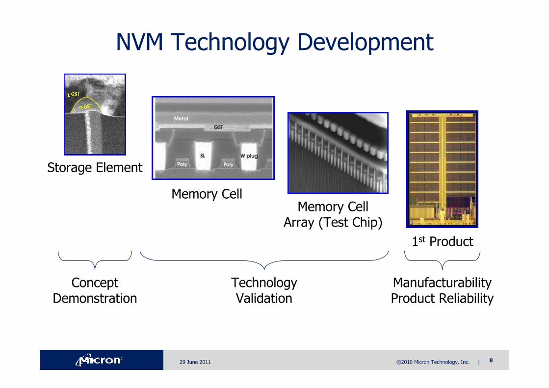
NVM Technology Development
Storage Element
Memory CellMemory Cell
Array (Test Chip)
1st Product
ConceptDemonstration
TechnologyValidation
ManufacturabilityProduct Reliability

©2010 Micron Technology, Inc. | 929 June 2011
Non-Volatile Memory History
1967 ���� First Floating Gate Structure
1971 ���� FAMOS
1977 ���� EPROM
1980 ���� EEPROM
1985 ���� 1T EEPROM (Flash)
1988 ���� NOR Flash
1989 ���� NAND Flash
1995 ����MLC NOR
2005 ���� MLC NAND
2010 � Intel-Micron 64Gb MLC NAND in 25nm technology

©2010 Micron Technology, Inc. | 1029 June 2011
History of PCM Development
2001 2003 2005 2007 2009 2011
M. Gill et al.,ISSCC 2002
180nm
G. Casagrande et al.,VLSI 2004
180nm
PCMcell
S. Lai and T. Lowrey,IEDM 2001
180nm
F. Pellizzer et al.,VLSI 2006
90nm
Bedeschi et al.,ISSCC 2008
90nm 128Mb (256Mb MLC)
G. Servalli,IEDM 2009
45nm
PCM array& chip
F. Pellizzer et al.,VLSI 2004
180nm
C. Villa et al.,ISSCC 201045nm 1Gb
ConceptDemonstration
Technology ValidationProduct Reliability
Manufacturing
©2010 Micron Technology, Inc. | 1129 June 2011
Key Messages
• Significant Innovation Takes Time
• A NVM Concept/Technology Must Have a
Wide Spectrum of Application

©2010 Micron Technology, Inc. | 1229 June 2011
Phase Change Memory Key Attributes
105 -106
200-200 ns
13-30
KB/s
~Flash
Easy
No
Small/Byte
n.a.
Yes
EEPROM
NoYesYesNoErase
20 - 80 ns15 - 50 us70-100 ns50 - 100 nsRead Latency
100+
MB/s
10+
MB/s
0.5-2
MB/s
1- 15+
MB/s
Write Bandwidth
EasyHardModerateEasySoftware
High~Flash~Flash~FlashPower
Small/ByteLargeLargeSmall/ByteGranularity
NoYesYesYesNon-Volatile
3x nm2x nm3x nmsub-2x nmScaling
104-5
NAND
Unlimited
DRAM
105
NOR
106+Endurance
PCMAttributes
PCM provides an new set of features combining components of NVM with DRAM
• Non Volatility
• Flexibility
▶ No Erase, Bit
alterable, Continuous
Writing
• Lower power consumption than RAM
• Fast Writes
• Read bandwidth and writing throughput
• eXecution in Place
• Extended endurance
©2010 Micron Technology, Inc. | 1329 June 2011
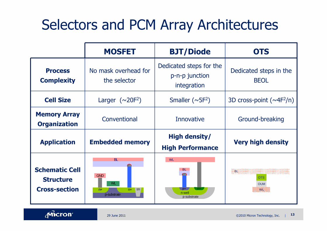
Selectors and PCM Array Architectures
High density/
High Performance
Innovative
Smaller (~5F2)
Dedicated steps for the
p-n-p junction
integration
BJT/Diode
Very high densityEmbedded memoryApplication
Schematic Cell
Structure
Cross-section
Memory Array
Organization
Cell Size
Process
Complexity
Ground-breakingConventional
3D cross-point (~4F2/n)Larger (~20F2)
Dedicated steps in the
BEOL
No mask overhead for
the selector
OTSMOSFET
n+n+p-substrate
STI
WL
BL
GND
n+n+p-substrate
STI
WL
BL
GND
p-substraten-wellp+
BL
WL
n+
p-substraten-wellp+
BL
WL
n+
BL
WL
OUM
OTS
©2010 Micron Technology, Inc. | 1429 June 2011
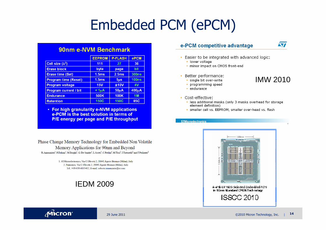
Embedded PCM (ePCM)
IEDM 2009
IMW 2010

©2010 Micron Technology, Inc. | 1529 June 2011
Stand-Alone NVM TAM Expansion
Bulk NANDBulk NAND
Industrial / CEIndustrial / CE
SSDSSD
WirelessWireless
Cost, Cost & Cost!!!}
} Cost, Reliability, & Performance
Source: iSuppli Application Market Forecast Tool , June 2010
($K)

©2010 Micron Technology, Inc. | 1629 June 2011
PCM Application Opportunities
PCM feature can be exploited by all the memory system, especially the ones resulting from the convergence of consumer, computer and communication electronics
• Wireless System to store of XiP, semi-static data and files▶ Bit alterability allows direct-write memory
• Solid State Storage Subsystem to store frequently accessed pages and elements easily managed when manipulated in place▶ Caching with PCM will improve performance and reliability
• Computing Platforms taking advantage of non-volatility to reduce the power▶ PCM offers endurance and write latency that are compelling for a number of
novel solutions
S.Eilert et al., “PCM: a new memory enables new memory usage models”, IMW, 2009

©2010 Micron Technology, Inc. | 1729 June 2011
MLC Capability
“Write Strategies for 2 and 4-bit Multi-Level Phase-Change Memory”IBM/Macronix, IEDM 2007
“A Multi-Level-Cell Bipolar Selected Phase Change Memory”Numonyx, ISSCC 2008
“Drift-Tolerant Multileve Phase Change Memory”IBM, IMW 2011
©2010 Micron Technology, Inc. | 1829 June 2011
Key Messages
• Significant Innovation Takes Time
• A NVM Concept Must Have a Wide
Spectrum of Application
• A New NVM Must Be Scalable

©2010 Micron Technology, Inc. | 1929 June 2011
C. Lam, SRC NVM Forum 2004
Y. C. Chen et al., IEDM 2006
Ultimate Scalability of PCM
• Device functionality demonstrated
on 60 nm2 active area
• Reset current <10uA
• Phase change mechanism appears
scalable to at least ~5nm
P.Wong, EPCOS 2010

©2010 Micron Technology, Inc. | 2029 June 2011
Outline
• Non Volatile Memories Status
• The Phase Change Memories
• An Outlook to the Next Steps
©2010 Micron Technology, Inc. | 2129 June 2011
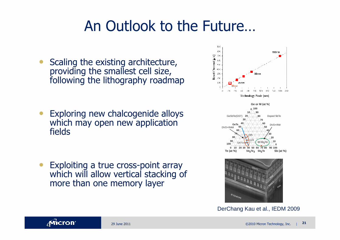
An Outlook to the Future…
• Scaling the existing architecture, providing the smallest cell size, following the lithography roadmap
• Exploring new chalcogenide alloys which may open new application fields
• Exploiting a true cross-point array which will allow vertical stacking of more than one memory layer
Ge or M (at %)
0 100
90
80
7060
5040
3020
100
1020
30
4050
6070
80
90100
60 70 80 90 10050403020100Sb (at %)Te (at %)
GeTe
Sb2Te3
GeSbTe(GST) Doped SbTe
Sb2Te
M-Sb2Te
DVD+RW
225
147
DVD+RAM
124
DerChang Kau et al., IEDM 2009
©2010 Micron Technology, Inc. | 2229 June 2011
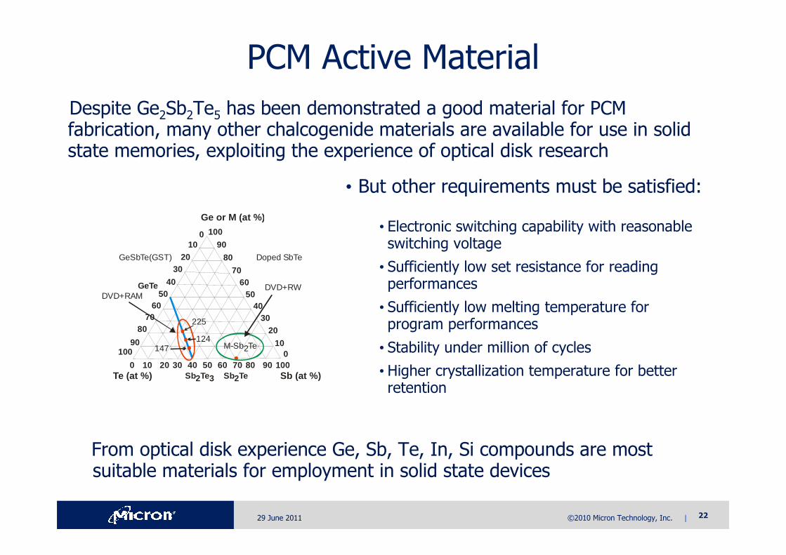
PCM Active Material
Ge or M (at %)
0 100
90
80
7060
5040
3020
100
1020
30
4050
6070
80
90100
60 70 80 90 10050403020100Sb (at %)Te (at %)
GeTe
Sb2Te3
GeSbTe(GST) Doped SbTe
Sb2Te
M-Sb2Te
DVD+RW
225
147
DVD+RAM
124
• But other requirements must be satisfied:
• Electronic switching capability with reasonable switching voltage
• Sufficiently low set resistance for reading performances
• Sufficiently low melting temperature for program performances
• Stability under million of cycles
• Higher crystallization temperature for better retention
From optical disk experience Ge, Sb, Te, In, Si compounds are most suitable materials for employment in solid state devices
Despite Ge2Sb2Te5 has been demonstrated a good material for PCM fabrication, many other chalcogenide materials are available for use in solid state memories, exploiting the experience of optical disk research

©2010 Micron Technology, Inc. | 2329 June 2011
GST Ternary Diagram
• GeSbTe ternary compound system
• GeTe – Sb2Te3
pseudo-binary line
• Sb – rich region exploration is done to electrically study new compounds in the fast growth Sb69Te31 direction
Goal: improve the cell performances
M. Boniardi et al., IMW 2010

©2010 Micron Technology, Inc. | 2429 June 2011
Electrical Characteristics
• Decrease of the reset resistance with the increase in the Sbconcentration
• Convergence of the set level to the minimum set

©2010 Micron Technology, Inc. | 2529 June 2011
“Electrical Performances of Tellurium-rich Gex-Te1-xPhase Change Memory”
CEA-LETI/ST, IMW 2011
“On Carbon doping to improve GeTe-basedPhase-Change Memory data retention at
high temperature”CEA-LETI/ST, IMW 2010
“N-doped GeTe as Performance Booster for Embedded Phase-Change Memories”
CEA-LETI/ST, IEDM 2010
Higher-Temperature Chalcogenide

©2010 Micron Technology, Inc. | 2629 June 2011
Further Key Materials
• Other key issue of the PCM cell engineering are:
▶ Role of thermal environment: thermal conductivity of the surrounding dielectrics
▶ Role of thermal interfaces between materials
▶ Role of electrical interface between materials

©2010 Micron Technology, Inc. | 2729 June 2011
PCM Self-Heating Cell Structure
Vertical self-heating structure with fully confined GST �very conformal chalcogenide deposition required (e.g. ALD)
Planar structures
2010 Symp. On VLSI Tech.Samsung

©2010 Micron Technology, Inc. | 2829 June 2011
3D Integration Cross-Point Memory
• Crossbar memory attracts great interests
▶ “simple” structure and minimum cell size (4F2)
� low cost
▶ suitable for 3D stacking � cell size (4/n)F2
▶ array over circuitry � better array efficiency
• The basic cell architecture requires a
selector structure to be integrated in the
BEOL
▶ Parasitic paths exist through neighbouring cells
▶ Programming (and also reading) can perturb
the array
Vprog
0 V
Vprog/2
Vprog/2
Vprog/2 Vprog/2

©2010 Micron Technology, Inc. | 2929 June 2011
A Wide Range of Material Choices
• Homojunctions � polySi p/n junctions
• Heterojunctions � p-CuO/n-InZnO
• Schottky diode� Ag/n-ZnO
• Chalcogenide Ovonic Threshold Switching (OTS) materials
• Mixed Ionic Electronic Conduction (MIEC) materials
• STTRAM
• RRAM or CBRAM
• PCM
Selector device Storing device
For the selector structure few
concepts have been proposed so
far, all in the “path finding” phase
©2010 Micron Technology, Inc. | 3029 June 2011
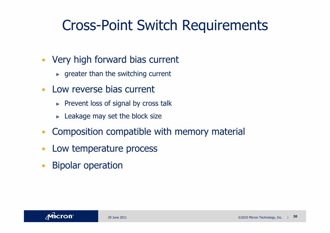
Cross-Point Switch Requirements
• Very high forward bias current
▶ greater than the switching current
• Low reverse bias current
▶ Prevent loss of signal by cross talk
▶ Leakage may set the block size
• Composition compatible with memory material
• Low temperature process
• Bipolar operation

©2010 Micron Technology, Inc. | 3129 June 2011
PCMS Memory Cell Cross-Bar Architecture
Ovonic Threshold Switch, OTS, is a two-terminal switch
Metal 1Met
al 2
Row
Column
Poly
Si-Subst rate
Metal 1Met
al 2
Row
Column
Poly
Si-Subst rate
Chalcogenide materials can be used both for the memory and for
the selector (OTS) to form stackable cross point PCM (PCMS)
•True high density cross-bar
•Possible multilayer vertical stacking
Intel-Numonyx, IEDM 2009

©2010 Micron Technology, Inc. | 3229 June 2011
Conclusions
• The mainstream Non-Volatile Memory (Flash) is today
approaching its scaling limitation
• Several other alternative concepts have been proposed but
few of them are really appealing from a cost stand point
• Among those technology, PCM is today in a privileged
position, having already demonstrated functionality and
reliability at 90 nm and 45 nm nodes on large products
• Large room for chalcogenide material and cell engineering
• Crossbar 3D approach has been identified as a viable way
to further reduce the cost/bit

July 11