a tem cell design to study electromagnetic radiation exposure from
TRANSCRIPT

A TEM CELL DESIGN TO STUDY ELECTROMAGNETIC RADIATION
EXPOSURE FROM CELLULAR PHONES
A Thesis
presented to
the Faculty of the Graduate School
at the University of Missouri
In Partial Fulfillment
of the Requirements for the Degree
Master of Science
by
NATTAPHONG BORIRAKSANTIKUL
Dr. Naz E. Islam, Thesis Advisor
AUGUST 2008

The undersigned, appointed by the dean of the Graduate School, have examined the
thesis entitled
A TEM CELL DESIGN TO STUDY ELECTROMAGNETIC RADIATION
EXPOSURE FROM CELLULAR PHONES
presented by Nattaphong Boriraksantikul,
a candidate for the degree of Master of Science in Electrical Engineering,
and hereby certify that, in their opinion, it is worthy of acceptance.
Naz E. Islam _______________________________________________________
Professor Naz E. Islam
William (Bill) C. Nunnally _______________________________________________________
Professor William (Bill) C. Nunnally
H. R. Chandrasekhar _______________________________________________________
Professor H. R. Chandrasekhar

ii
ACKNOWLEDGEMENTS
I would like to express my special thank to my advisor, Dr. Naz E. Islam, who has
provided me with many research opportunities at his High Power Electromagnetic
Research (HiPER) laboratories and this thesis work in particular. His suggestions and
support were extremely valuable. I would also like to thank Dr. William (Bill) C.
Nunnally who first introduced me to research scenario while at MU. I also thank Dr. H.R.
Chandrasekhar who is a member of my thesis committee for providing valuable
comments and suggestions.
Thanks are also due to my HiPER laboratory colleagues and friends who have
contributed towards this project directly or indirectly. I would also like to sincerely thank
Dr. Phumin Kirawanich, a senior researcher at Dr. Islam’s High Power Electromagnetic
Research (HiPER) laboratories, for helping me in my research. At the campus level I
thank all of my friends, who, during my stay here, have provided me the wonderful
company while participating in sports, camping, and entertainment.
Finally, I am very grateful to my parents, older brother, younger brother, and
younger sister for their selfless love and supports. Without the love, affection and prayers
of my family I would not have accomplished as much.
Nattaphong Boriraksantikul July, 2008

iii
A TEM CELL DESIGN TO STUDY ELECTROMAGNETIC RADIATION EXPOSURE FROM CELLULAR PHONES
Nattaphong Boriraksantikul
Dr. Naz E. Islam, Thesis Supervisor
ABSTRACT
A transverse electromagnetic (TEM) cell was designed and fitted with a double
ended monopole antenna as a signal leader in order to couple electromagnetic radiation
from GSM 900 and 1800 commercial cellular phones into a usable area of the cell. The
double-ended monopole antenna acts as a signal leader for incoming and outgoing signals
between the TEM cell’s outer surfaces. Biological subjects can be placed at the usable
area for biological effects of electromagnetic radiation studies.
The amplitudes of the forward and backward travelling mode excitation and the
input impedance of the signal leader were analyzed in the study. It showed good
agreement with known results from other experiments and lab simulations. The electric
field distribution was studied with such varying parameters as the cellular phone position,
polarization, dialing type, and dialing frequency.
Analysis showed that the electric field uniformity can be improved with either the
use of a shorter signal leader or by reducing the dimensions (size) of the TEM cell. The
test area available in this design is large enough for a Petri dish, such that electromagnetic
radiation studies can be performed. Another advantage of the setup is that, unlike
cuvettes, cells can be of a single layer (grown on the dish) and thus the shielding effects
of one cell on the other while under electromagnetic radiation can be minimized.

iv
TABLE OF CONTENTS
ACKNOWLEDGEMENTS ........................................................................ ii
ABSTRACT ................................................................................................ iii
LIST OF FIGURES ................................................................................... vi
Chapter 1: Introduction .............................................................................. 1
Chapter 2: Literature Review .................................................................... 5
Chapter 3: Theoretical Background ........................................................ 23
3.1 Transmission Lines ...................................................................................... 23
3.2 Waveguides ................................................................................................... 27
3.3 Mode Excitation ........................................................................................... 33
3.4 Transverse Electromagnetic Cell or TEM Cell ......................................... 35
3.5 Monopole Antenna ....................................................................................... 40
3.6 Magnetic Field Probe ................................................................................... 42
Chapter 4: Experimental and Simulation Configurations .................... 44
4.1 Simulation Configuration …………............................................................ 44
4.1.1 TEM Cell Characteristics ................................................................ 44
4.1.2 Simulation Setup of Cellular Phone Measurement ......................... 47
4.1.3 Simulation to Improve of Electric Field Uniformity ...................... 48
4.2 Experimental Configuration ....................................................................... 49
4.2.1 Construction of TEM Cell .............................................................. 49
4.2.2 Construction of Electric Field Probe ............................................... 51
v
4.2.3 Construction of Magnetic Field Probe ............................................ 52
4.2.4 Measurement Procedures ................................................................ 53
4.2.5 Improvement of Electric Field Uniformity ..................................... 58
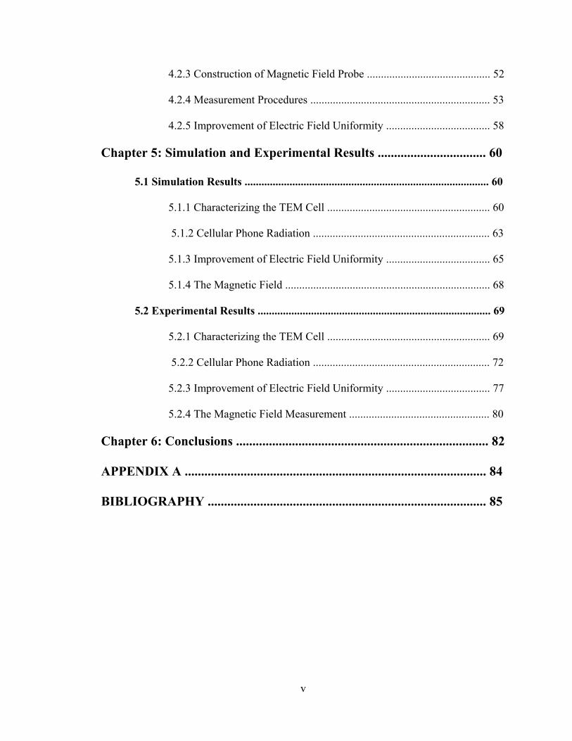
Chapter 5: Simulation and Experimental Results ................................. 60
5.1 Simulation Results ....................................................................................... 60
5.1.1 Characterizing the TEM Cell .......................................................... 60
5.1.2 Cellular Phone Radiation ............................................................... 63
5.1.3 Improvement of Electric Field Uniformity ..................................... 65
5.1.4 The Magnetic Field ......................................................................... 68
5.2 Experimental Results ................................................................................... 69
5.2.1 Characterizing the TEM Cell .......................................................... 69
5.2.2 Cellular Phone Radiation ............................................................... 72
5.2.3 Improvement of Electric Field Uniformity ..................................... 77
5.2.4 The Magnetic Field Measurement .................................................. 80
Chapter 6: Conclusions ............................................................................. 82
APPENDIX A ............................................................................................ 84
BIBLIOGRAPHY ..................................................................................... 85

vi
LIST OF FIGURES
Figure 2.1 The TEM cell was first designed by Crawford:
(left) top view, and (right) cross view ……………….…..……….………… 6
Figure 2.2 The experimental system diagram of the absorbed power
analyzer is by John R. Juroshek, and Cletus A. Hoer. …………….....…..… 8
Figure 2.3 The normalized electric field in the longitude along the
length of the TEM cell at 80 MHz. This result is by
Xiao-Ding Cai, and G. I. Costache. …………………………………….…. 10
Figure 2.4 The normalized electric field in the longitude along the
length of the TEM cell at 90 MHz. This result is by
Xiao-Ding Cai, and G. I. Costache. ……………………………………..… 11
Figure 2.5 The simulation of electric field in perpendicular direction
to the inner conductor at 837 MHz. This result is by
Popovoc, Susan C. Hagness, and Allen Taflove. …………….…………… 13
Figure 2.6 The simulation of SAR within the culture dishes placed on
the top of the inner conductor inside the TEM cell. The results
were simulated 3 mm above the inner conductor along the
longitudinal of the TEM cell with varies of the dish thickness.
This result is by Popovoc, Susan C. Hagness, and Allen Taflove. ……….. 14
Figure 2.7 The IC experiment setup using the TEM cell by Ronald De Smedt,
Steven Criel, Frans Bonjean, Guido Spildooren, Guy Monier,

vii
Bernard Demoulin, and Jacques Baudet ………………………………...… 15
Figure 2.8 Cross section view of the Experimental setup system.
The microstrip line is attached at the top of the ceiling inside
the TEM cell. The port 1 is the current feeder. The port 2 is the load
impedance. The port 3 and 4 are matched impedances.
This diagram is by Franco Fiori, and Francesco Musolino. ………………. 17
Figure 2.9 The experimental scheme of RF exposure of human lymphocytes
by Ruslan Sarimov, Lars O.G. Malmgren, Eva Markova,
Bertil R. R. Persson, and Igor Y. Belyaew …………………………...…… 20
Figure 3.1 The transmission line schematics; (left) voltage and current
definition, and (right) lumped-element equivalent circuit.
This figure is from the Testing for Microwave Engineer book [24]. ……... 23
Figure 3.2 Photograph of various rectangular waveguides …………………………… 27
Figure 3.3 Geometry of the rectangular waveguide. This figure is from
the Testing for Microwave Engineer book [24]. .…………………………. 29
Figure 3.4 TE modes in the waveguides ……………………………………………… 32
Figure 3.5 The arbitrary electric or magnetic current source in wavelengths.
This figure is from the Testing for Microwave Engineer book [24]. ……... 33
Figure 3.6 The rectangular TEM cell ……………………………………………….… 35
Figure 3.7 Cross section view of the TEM cell …………………………………….… 36
Figure 3.8 The ideal field strength plots with various heights above and
below the septum ………………………………………………………….. 38
Figure 3.9 The construction of the electric field probe. This figure is

viii
from the Testing for EMC Compliance book [26]. ……………………..… 41
Figure 3.10 The construction of the magnetic loop probe. This figure is
from the Testing for EMC Compliance book [26]. ……………..………… 42
Figure 3.11 The magnetic loop probe model. This figure is from the
Testing for EMC Compliance book [26]. …………………………………. 43
Figure 4.1 The parameters of the TEM cell dimension …………………………….… 44
Figure 4.2 The CST model of the TEM cell: outside view (above),
and inside view (bottom) ………………………………………………..… 45
Figure 4.3 Input signal port (left), and 50-ohms impedance load (right) …………..… 46
Figure 4.4 Boundary condition ……………………………………………………..… 46
Figure 4.5 The double-ended monopole antenna is attached to
the outer conductor. ...…………………………………………………….. 47
Figure 4.6 The signal leader was attached with the outer conductor of
the TEM cell. ……………………………………………………………… 47
Figure 4.7 The smaller TEM cell dimensions ……………………………………..….. 48
Figure 4.8 The constructed septum (left); The septum dimensions (right) ……….….. 49
Figure 4.9 The constructed tapered section parts (left); The tapered section
part dimensions (right) ………………………………………………….… 49
Figure 4.10 The constructed rectangular transmission section part (left);
The rectangular transmission section part dimensions (right) ………….… 50
Figure 4.11 The completed TEM cell ……………………………………………….… 50
Figure 4.12 The electric field probe components by Scott Roleson [30] ……………… 51
Figure 4.13 The laboratory constructed electric field probe …………………………… 51

ix
Figure 4.14 Covering the paper clip with the insulator. This figure is
from the Testing for EMC Compliance book [26]. ……………………..… 52
Figure 4.15 The laboratory constructed magnetic field probe ………………………..... 53
Figure 4.16 The experimental setup of characterizing the TEM cell’s impedance ….… 54
Figure 4.17 The observation points on the top of the TEM cell …………………..…… 55
Figure 4.18 The experimental setup of the electric field distribution measurement ...… 55
Figure 4.19 Experimental setup for the cellular phone near-field EM exposure
using the laboratory constructed TEM cell .…………………………….… 56
Figure 4.20 Positions and directions of the cellular phone: (a) locating the
cellular phone at level A outside the TEM cell and placing the
cellular phone in X, Y, Z directions, (b) attaching the cellular
phone with the outer conductor inside the TEM cell and placing
the cellular phone in X, Y, Z directions, and (c) locating the
cellular phone on the top of the inner conductor inside the
TEM cell and placing the cellular phone in X, Y, Z directions .………….. 57
Figure 4.21 The laboratory constructed smaller TEM cell …………………………….. 59
Figure 5.1 TDR result represented the characteristic impedance of the TEM cell …… 60
Figure 5.2 VSWR result of the TEM cell …………………………………………….. 61
Figure 5.3 Cross view of the electric field contour inside the
TEM cell at 100 MHz .……………………………………………………. 62
Figure 5.4 VSWR result of the TEM cell with the 9.4 cm double-ended monopole
antenna …………………………………………………………………….. 63
Figure 5.5 (Top) configuration of the TEM cell and the signal leader used in the

x
simulation. (Bottom) top view of normalized resulting electric field
distribution when the cellular phone is dialing. …………………………... 64
Figure 5.6 VSWR result of the TEM cell with the 1 cm double-ended monopole
antenna …………………………………………………………………..… 65
Figure 5.7 Top view of simulated electric field distributions of the 1-cm signal
leader as referenced to the 9.4 cm signal leader ………………………...… 66
Figure 5.8 Simulated results of the VSWR and the electric field distribution (inset)
of the smaller TEM cell .………………………………………………...… 67
Figure 5.9 The simulation of the magnetic field in Y direction at 500 MHz of the
smaller TEM cell at 2 cm above the septum ……………………………… 68
Figure 5.10 Characteristic impedance results of the TEM cell ………………………… 69
Figure 5.11 Experimental VSWR result of the TEM cell ……………………………… 70
Figure 5.12 Experimental results of the electrical field at 100 MHz and 2 cm
above the septum ………………………………………………………..… 71
Figure 5.13 The electrical field distribution observed from the top view …………...… 72
Figure 5.14 Each cell phone’s position in experiment and the electric field results.
The arrow’s pointing out the cell phone represents calling out, and the
arrow’s pointing to the cell phone represents calling in. The electric field
results were measured at 3.5 cm from the outer conductor ………...…..…. 74
Figure 5.15 Profiles of the normalized electric field distribution at 825.125 MHz
on the yz plane during establishing with calling-in and out signals
at different cellular phone locations. (a) location A, calling-in signal,
(b) location B, calling-in signal, (c) location C, calling-in signal,

xi
(d) location A, calling-out signal, (e) location B, calling-out signal,
and (f) location C, calling-out signal .……………………………………... 75
Figure 5.16 VSWR measurement of the TEM cell with the 9.4 cm signal leader
and TEM cell ports connected to the network analyzer ……………...…… 76
Figure 5.17 VSWR measurement of the TEM cell with the 1 cm signal leader
and TEM cell ports connected to the network analyzer …………………... 77
Figure 5.18 Electric field distributions of the 1-cm signal leader as referenced
to the 9.4 cm signal leader. (a) and (b) are the measured profiles of the
normalized electric field distribution with the shorter signal leader
at 825.125 MHz during calling in and calling out, respectively ………..… 78
Figure 5.19 The experimental VSWR result of the smaller TEM cell ………………… 78
Figure 5.20 The normalized electric field distributions in X direction of the
smaller TEM cell at 2 cm above the septum. (a) and (b) are the
measured profiles of the normalized electric field distribution at
1800 MHz during calling in and calling out, respectively …………….….. 79
Figure 5.21 The magnetic field in Y direction at 500 MHz of the smaller TEM cell
measured 2 cm above the septum ……………………………………….… 80
1
Chapter 1: Introduction
Communicating with other members of the species has always been essential for
humans and other living things. It is a means through which humans and other living
creatures share valuable information that are necessary for everyday living and for
survival. While limited research has been conducted on the advances and developments
of the methods through which different animals communicate with each other, we are
fully conversant with human communication methods and how they have evolved and
changed dramatically through the ages - ranging from smoke signals to the use of the
Morse code to satellite based communications through various electronic means.
Before the advent of electronic mails, short message services (SMS), and cellular
phones most of the communications were through letters or telegraphs, and occasionally
wire (LAN lines) were used for talking to each other through phones. Following a rapid
change in the last two decades, the use of the cellular phones has become the most
popular mode of communication for most people across the globe. It is the most common
media for making connections with each other and the cost involved is within most
people’s budget. In addition the devices are easy to carry everywhere. With the passage
of time, the dimensions of the cellular phones becomes smaller and smaller and the
functions associated with the gadget have also increased many fold, where many ‘smart
phones’ now include electronic mail, calendar and other essential for keeping in touch
with the workplace. The number of users of the cell phone has also grown many folds
and is perhaps the most common mode of communication, not only between different
individuals but for members of the same family as well.

2
It was estimated that there are 3.3 billion people using the cellular phones by
November, 2007 [1]. It is also estimated that on a given day, while we are walking on the
street, there are at least one-fourth of the population talking on the cellular phone. It is not
uncommon to hear the cellular phone ringing in the cinema in any show. Even in the
class room, many students would not turn off the phone ring. By 2010, it is also estimated
that around 90 percents of the world’s populations will be using the cellular phones in
their everyday life.
At the same time, there are concerns about the cellular phone radiation effects and
it is felt that the public should be aware of the dangers of electromagnetic radiation. Some
are wondering whether the cellular phone can affect to human health because of
electromagnetic (EM) radiation of the cellular phone. People believe that it causes brain
tumor, cataracts, or Alzheimer. However, it is still a question. There are many researches
being studied on the cellular phone radiation effects [2]-[5].
The maximum power absorption of the head tissue from the cellular phone
radiation, expressed in SAR, allowed by the FCC is 1.6 W/kg in 1 g. When the
microwave radiation is emitted from the cellular phone, the tissues in the head and neck
regions of the human body will absorb it. The 50 percents of the radiation is deposited
into such tissues as the ear, scalp, skull, and the brain [2]. This can cause the excess heat
of the brain’s blood circulation. Therefore, the measurement of the EM radiation
strengths from the cellular phone is need.
In general, an anechoic is a large shielded room. The anechoic chamber provides
the uniformity of the EM fields and the shield environment. It is mainly used for the
radiated emission and the immunity measurement. In the case of the emission, it is able to

3
generate the real signals, so there is no need to consider the ambient signals. In the case
of immunity testing, the anechoic chamber can provide the uniform EM fields, so it will
prevent any potential interferences or field distributions.
The use of large test areas for measurements and conducting experiments such as
an anechoic chamber or open area test site (OATS) are not efficient when the biological
samples are very small. For smaller samples a defined area with minimum interference
and reflection of the EM signal area is required and large test chambers do not meet this
requirement. On the other hand, a transverse electromagnetic (TEM) cell, which consists
of a rectangular coaxial transmission section tapered with coaxial connectors on both
ends, is a better choice and provides a uniform EM field in a shielded environment [6].
The usable area of the TEM cell is one-third of volume between the inner and the outer
conductors. It is used generally for radiated immunity and emission tests of electronic
devices [6]-[7], and biological applications [8].
In this thesis, an experiment method to capture and project a cell phone signal into
a confined and shielded area in order to study the effects of it electromagnetic radiation is
described. Specifically, the cell phone signal is captured and projected inside the usable
area of a TEM cell that was designed and constructed in the laboratory. The thesis also
describes the function of the double-ended monopole antenna attached to the TEM cell’s
outer conductor and the cell phone used in the experiment, specifically the frequencies
ranges that are established between the cellular phone and the base stations. The
amplitudes of the forward and backward travelling mode excitation and the input
impedance of the signal leader are also analyzed. The coupled voltage and
electromagnetic field distribution were studied with the cellular phone position,

4
polarization, dialing type, and dialing frequency. The results between experiments and
simulation were compared.
Following this brief introduction, chapter 2 will start with the various techniques
of exposing the cellular phone radiation. In Chapter 3 the several theories related with the
measurement are described. A detailed explanation of the experiment setup and the
various components used in the experiment, such as an AT&T Motorola C139, a double-
ended monopole antenna, an Agilent E7402A spectrum analyzer, and measurement
procedure are discussed in Chapter 4. The measurements, simulation results and analysis
and discussion related to the experiment are detailed in Chapter 5. The last chapter,
Chapter 6, includes the conclusion and suggests future work that can be done in order to
carry he work forward.

5
Chapter 2: Literature Review
The central theme of this work is on the design and development of a TEM cell
for studies related to the effects of electromagnetic radiation from a TEM cell. As such,
we begin with a brief introduction of the research related to TEM cells and its usage. We
discuss the necessity, theory and application of TEM cells. We also discuss some of the
relative advantages and disadvantages of TEM cell use as compared to other devices in
electromagnetic field susceptibility studies etc.
The transverse electromagnetic (TEM) transmission cell was first introduced by
Myron L. Crawford at the National Bureau of Standards in 1973 [9]. In 1974, Crawford
realized that the electronic or electromechanical systems in the open systems would affect
the level and number of potential interfering signals. For this reason, he presented the
TEM cell for establishing uniform electromagnetic fields in a shielded environment [6]. It
operates at broad band frequency, which is restricted by the waveguide multimode
frequency associated with the cell size. For the theoretical TEM cell, I will mention in the
next chapter.
Crawford designed the TEM cell to operate as 50 ohm impedance-matched
systems. It consists of a rectangular coaxial transmission section tapered with coaxial
connectors on the both ends, as shown in Fig. 2.1. His design considerations were to
maximize usable test cross sectional area, maximize upper useful frequency limit,
minimize cell impedance mismatch or voltage standing wave, and maximize uniformity
of EM field pattern characteristic of the cell. He also presented the equation for the
characteristic impedance of the TEM cell, which is the approximate same as the equation

6
for the characteristic impedance of the shielded strip line. This theoretical concept will be
discussed in the next chapter.
Since the TEM cell was introduced by Crawford, it has been used in many
applications. Applications include electromagnetic radiation effects to biological objects,
electromagnetic compatibility (EMC) test chips, higher order modes inside the TEM cell,
investigation of the electric field uniformity in the culture media, the cellular phone
radiation effects to the biological cells, the radio frequency radiation effects to
pharmaceuticals, the electromagnetic field effects to mollusk neurons, and testing of
integrated circuit emissions and more.
Fig. 2.1 The TEM cell was first designed by Crawford: (left) top view, and (right) cross view.
7
An important application of TEM cell research related to this work is the study of
input impedance of a probe in the TEM cell. This study was presented by Perry F.
Wilson, David C. Chang, and Mark T. MA in 1984 [10]. They have investigated the
excitation of the rectangular transmission section of the TEM cell, which is caused by a
vertical probe. It was realized that since antennas would be placed inside the TEM cell
for exciting or measuring the EM field, or feeding the signal to the electronic equipment,
this would affect the excitation of the TEM mode and the field distribution inside the
TEM cell.
The expression for the input impedance of the probe antenna exciting the TEM
cell was based on a number of considerations. The equations were developed as an
antenna in a rectangular waveguide and based on the assumption that the gap between the
inner conductor and outer shields was both electrically small and short compared to the
cell width. To analyze the equations, the authors suggested understanding the Green’s
function due to evaluating the variation impedance integral. The authors showed the input
impedance results in two terms: the ordinary rectangular waveguide contribution and the
gap perturbation impedance.
The ordinary rectangular waveguide contribution term is considered as the input
impedance factor because of the vertical probe in the rectangular waveguide containing
the probe. For the gap perturbation term, since the dominant TEM mode is not able to
propagate when the gaps are closed, this term contains the radiation resistance. The
authors contend that when the TEM mode radiation resistance value is taken out, then the
remaining principal contribution is reactive and less than the highly capacitive the
ordinary rectangular waveguide term. Therefore, the gap perturbation terms can be

8
ignored. This is a simple approximation to formulate the input impedance of a vertical
probe. The authors also provided the special examples to support their expressional
solution. This paper is very important since, in this thesis, the double-ended monopole
antenna has been used and inserted between the free space outside and inside the TEM
cell. It is therefore important to know and understand how to determine the input
impedance of a probe, which excites the TEM cell.
The second application of the TEM cell is the study of the high-power automatic
network analyzer for measuring the RF power absorbed by biological samples in the
TEM cell. This paper was presented by John R. Juroshek and Cletus A. Hoer in 1984
[11]. In this paper, the authors described the RF power-absorption analyzer, which was
used for measuring the power absorption of the biological test objects with continuous-
wave RF radiation in the TEM cell. It was developed by the National Bureau of Standard
for the National Institute for Occupational Safety and Health.
Fig. 2.2 The experimental system diagram of the absorbed power analyzer is by John R. Juroshek, and Cletus A. Hoer

9
The design, calibration, and the performance of the analyzer were presented. The
analyzer has been developed from a six-port automatic network analyzer, which is
capable to detect the small amounts of power absorption in the test objects. The six-port
network analyzer provides accurate data, and is able to easily repeat the measurements.
The six-port network analyzer is also able to detect some malfunctions and the errors of
calibration system. The system diagram of their experiment was shown in Fig. 2.2.
The TEM cell was operated at 1 to 1000 W for the incident power, and the
frequency in range of 100 to 1000 MHz. The authors expected to be able to gain the
absorbed power levels of 0.05 percent of the incident power. The results showed that the
absorber absorbed 0.02 to 0.05 percent of the incident power. The authors also compared
their experimental absorbed power measurement results of using the power absorption
analyzer and calorimetry. The average absorbed power from the analyzer was 3.6 watts,
and the average absorbed power from the calorimetry was 3.7 watts. Both the results
were in good agreement. This paper has provided an insight into biological applications
and studies using the TEM cell, and presents one of the methods of the experimental
setups for biological applications.
Another important TEM cell usage and application is the study of theoretical
modeling of longitudinal variations of electric field and line impedance in the TEM cell
by Xiao-Ding Cai, and G. I. Costache in 1993 [12]. The authors note that at that time the
TEM cell had been used generally for Electromagnetic Interference (EMI) and
Electromagnetic Compatibility (EMC) measurements. They have also pointed out that
there were many publications on the characteristic impedance, the transverse electric field

10
distribution, and the cut-off frequencies of higher order modes, yet all of them were
considered for the ideal case, that is, the center with cross- sectional area of the TEM cell.
The authors realized that while conducting experiments, an antenna or an electric
field sensor that is used are usually placed at the center position of the test area. Many
researchers, as a result, often assumed that the electric field at the center location inside
the TEM cell could be estimated by using theoretical results, determined through the
analyses of its transverse characteristic. However, it was not always correct since at high
operating frequency and near the first resonant, the VSWR is larger than 1.2, or the
antenna or the sensor is located away from the center position along the length of the
TEM cell. This will likely cause measurement errors, especially when calibrating the
antenna or the sensor before the experiment. The authors therefore proposed the study of
longitudinal characteristics of the TEM cell. They therefore presented the theoretical
equations of the longitudinal electric field and compared these theoretical results with the
Fig. 2.3 The normalized electric field in the longitude along the length of the TEM cell at 80 MHz. This result is by Xiao-Ding Cai, and G. I. Costache.

11
experiment results. Both results were in good agreement. This is shown in Fig. 2.3 and
Fig. 2.4. In this work, the methods described in this paper were used to compare the
longitudinal electric field results with my laboratory constructed TEM results.
The study of mode suppression in the TEM cell was studied by R. Lorch, and G.
Monich in 1996 [13]. The authors stated that the bandwidth of the TEM cell was limited
because of its resonance. They proposed a technique to eliminate the resonance by using
wall absorbers. There are two types of the waveguide modes: transversal electric (TE)
mode, and transversal magnetic (TM) mode. These modes appear above their cut-off
frequencies. There is any effect between the lowest modes cut-off frequency and its first
resonance. The resonance frequency is satisfied when the effective length of the TEM
cell is one-half wavelength of a higher mode.
R. Lorch and G. Monich also provided simulation results on how and where
higher modes were. They created a conducting device under test (DUT), which was
Fig. 2.4 The normalized electric field in the longitude along the length of the TEM cell at 90 MHz. This result is by Xiao-Ding Cai, and G. I. Costache.

12
placed at the bottom inside the TEM cell. The currents would flow on the DUT in the
vertical direction. The DUT caused the TE10 mode and the higher modes. To eliminate
these modes, there were three methods; the first method was splitting up the inner
conductor with the absorbers. The second option was placing the lossy straw absorbers
between the inner and the outer conductor, and the last method was wall absorbers, which
put the absorbers on the floor, the ceiling, and both side walls of the outer conductor.
The result, which was the TEM cell without the absorber, showed the first
resonant frequency at 450 MHz. However, when the authors split up the inner conductor
with the absorber, the frequency increased to 670 MHz. With the wall absorber method,
the result showed the increase in bandwidth up to 1 GHz. These results showed that the
bandwidth could be enlarged by using the absorbers. The results also showed that the first
resonant frequency could be expanded up to the double of the frequency. The knowledge
to eliminate the higher order modes, and enlarge the operating frequency was applied to
this work and are based on this paper,.
In 1996, Jens C. Rasmussen, Bernhard Scholl, Thomas Gellekum, and Hans J.
Schmitt used a fiber-optic polarimetric temperature sensor for characterizing a 900 MHz
TEM cell used in bio-effects dosimetry [14]. The authors presented comparing the
simulation results and the experiment results of SAR inside the liquid biological sample.
They also developed the optic polarimetric temperature probe to measure the SAR. The
probe could detect the temperature change lower than 0.003 °C. From this paper, one can
relate the work on the biological effects of the 900 MHz radiation, which is the in the
range of cellular phone radiation including the frequency in range of GSM 900 MHz.

13
Finite-difference time-domain (FDTD) analysis of a complete transverse
electromagnetic cell loaded with liquid biological media in culture dishes is presented by
Milica Popovoc, Susan C. Hagness, and Allen Taflove in 1998 [15]. The authors have
pointed out that in recent years the effects of EM field is of concern to many. The authors
have presented a method to study health risks of human exposure to the EM fields. They
have introduced the experimental setup by putting the biological cells in the culture
dishes, and placing them inside the TEM cell. Since the uniformity of EM field radiation
is critical to quantifying the biological response versus the electromagnetic dose, and EM
field non-uniformities are able to cause non-uniform exposure, the TEM cell has been
used to provide this uniformity condition.
Milica Popovoc, Susan C. Hagness, and Allen Taflove have presented the
simulations of high-resolution three-dimensional FDTD of the TEM cell as shown in Fig.
Fig. 2.5 The simulation of electric field in perpendicular direction to the inner conductor at 837 MHz. This result is by Popovoc, Susan C. Hagness, and Allen Taflove.

14
2.5. A number of key factors, which caused the non-uniform EM fields, were addressed.
The first is the longitudinal standing waves within the TEM cell. The second factor
defined by the research is the field distribution near the surface and edges of the inner
conductor. The third important factor is the wave reflections within individual tissue-
culture dishes. The final factor emphasized by the research is wave reflections between
adjacent tissue-culture dishes. In addition, the temperature within the culture dishes might
cause the non-uniformity fields because the culture media absorbs RF power. Fig. 2.5 is
the simulation results of the electric field in vertical direction at 837 MHz. The VSWR of
the electric field along the longitudinal of the empty TEM cell, which was 1.25, was
obtained by using the graph results.
Fig. 2.6 The simulation of SAR within the culture dishes placed on the top of the inner conductor inside the TEM cell. The results were simulated 3 mm above the inner conductor along the longitudinal of the TEM cell with varies of the dish thickness. This result is by Popovoc, Susan C. Hagness, and Allen Taflove.

15
Fig. 2.6 shows the SAR results 3 mm above the inner conductor along the central
longitudinal of the TEM cell with variety of the thickness of the glass bottom. The results
indicated the non-uniform nature of the electric field along the longitudinal direction. The
results also showed that the highest SAR values were located next to the dish wall for all
the glass-bottom thickness, and the lowest SAR values were located near the center of the
dish for all the glass-bottom thickness. Finally, the glass-bottom thickness also affected
the SAR values.
The authors in the paper also studied cases considering the depth of the culture
liquid and the orientation of the culture dishes. The results show that in each case studied
there is a significant electrical field distributions and the specific absorption rate (SAR)
distributions. Finally, the authors concluded that these experiments by using the TEM cell
provided the useful data in setting the EM exposure. This paper provides insight on how
to apply the FDTD method to the biological application.
Fig. 2.7 The IC experiment setup using the TEM cell by Ronald De Smedt, Steven Criel, Frans Bonjean, Guido Spildooren, Guy Monier, Bernard Demoulin, and Jacques Baudet.

16
TEM cell measurements of an active EMC test chip were presented by Ronald De
Smedt, Steven Criel, Frans Bonjean, Guido Spildooren, Guy Monier, Bernard Demoulin,
and Jacques Baudet in 2000 [16]. The authors indicated how harmful noise in circuits
would be generated if the EMC occurred in the integrated circuit (IC) components.
Consequently, the measures must be harder and more complex. Since a circuit consists of
many IC devices, this means that the EMC is the serious problems, and it needs to be
considered carefully. The experiment setup for such an experiment is shown in Fig. 2.7.
The noise effects inside the IC component were investigated by using the TEM cell. The
reason of using the TEM cell is that it is more suited for qualification when the direct
radiation measurements are closely related to reality. Another reason is that the
experimental setup is easier comparing to the anechoic chamber. The authors described
that experimentalists usually measure only the emission from the chip. However, the
authors had done additional experiments on the emission of the tracks which was
connected to the outputs of the component. The experimental results suggested that clock
frequency, inverting 50 percents of the output lines, number of output driver sections in
parallel, and the power supply voltage of the driver section had a clear influence on the
emission level. This paper gives a good review of an important application using the
TEM cell, which is the measurement of electric device emission.
Another paper on TEM cell application is the study of measurement of integrated
circuit conducted emissions by Franco Fiori, and Francesco Musolino in 2001 [17]. The
authors investigate ICs such as microprocessors and microcontrollers that could act as
primary sources of EM emissions. The authors explain that the voltage interruption at the
power supply and ground pins of the IC, and the signals at the input/output (I/O) pins are

17
able to generate the EM radiation because these pins are working as the antennas printed
circuit board (PCB). Moreover, the pulsed currents, which flow through IC package leads
and circuits, also generate radiations of interfering EM fields. Therefore, the EM
radiations need to be considered and reduced by using EMI filters at PCB and system
level.
For this reason, the authors presented a new approach for measuring of integrated
circuit (IC) emissions by using the TEM cell. The TEM cell was used to detect the
spectrum of pulsed current flowing through an IC pin. As shown in Fig. 2.8, the
experiment setup consisted of a microstrip line, which was inserted in a matched TEM
cell. The microstrip line was fed by the power at one end from the interfering source. The
current then flowed through the microstrip line, which carried the RF power, and
propagated into the TEM cell toward its terminations.
Fig. 2.8 Cross section view of the Experimental setup system. The microstrip line is attached at the top of the ceiling inside the TEM cell. The port 1 is the current feeder. The port 2 is the load impedance. The port 3 and 4 are matched impedances. This diagram is by Franco Fiori, and Francesco Musolino.
18
The authors have also provided a brief description of the evaluation of the
relationship between the current spectrum of the source and the spectrum of the radio
frequency (RF) power delivered to the TEM cell. They compared the conducted emission
between measurement results and evaluation results. Both these results were in
agreement. It deals extensively on how to setup of the radiation measurement for the
microstrip line which could be applicable to the current project.
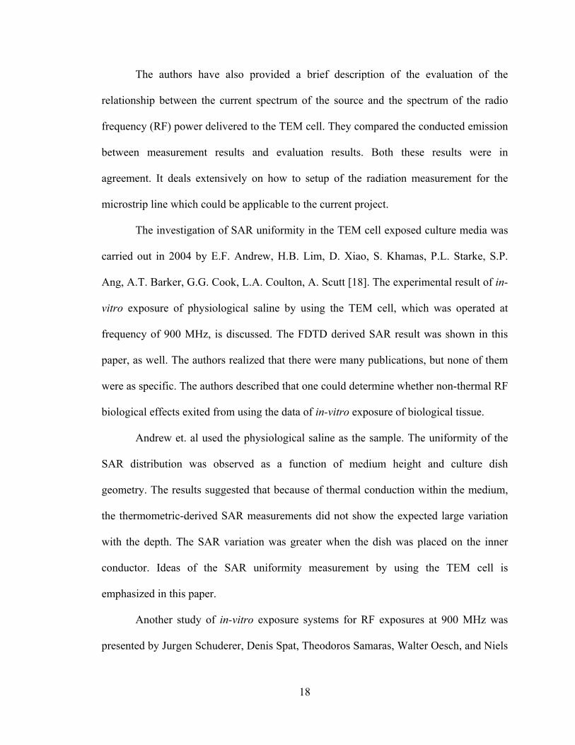
The investigation of SAR uniformity in the TEM cell exposed culture media was
carried out in 2004 by E.F. Andrew, H.B. Lim, D. Xiao, S. Khamas, P.L. Starke, S.P.
Ang, A.T. Barker, G.G. Cook, L.A. Coulton, A. Scutt [18]. The experimental result of in-
vitro exposure of physiological saline by using the TEM cell, which was operated at
frequency of 900 MHz, is discussed. The FDTD derived SAR result was shown in this
paper, as well. The authors realized that there were many publications, but none of them
were as specific. The authors described that one could determine whether non-thermal RF
biological effects exited from using the data of in-vitro exposure of biological tissue.
Andrew et. al used the physiological saline as the sample. The uniformity of the
SAR distribution was observed as a function of medium height and culture dish
geometry. The results suggested that because of thermal conduction within the medium,
the thermometric-derived SAR measurements did not show the expected large variation
with the depth. The SAR variation was greater when the dish was placed on the inner
conductor. Ideas of the SAR uniformity measurement by using the TEM cell is
emphasized in this paper.
Another study of in-vitro exposure systems for RF exposures at 900 MHz was
presented by Jurgen Schuderer, Denis Spat, Theodoros Samaras, Walter Oesch, and Niels

19
Kuster in 2004 [19]. The authors have pointed out that the studies of the health risk
influenced by RF electromagnetic field exposures usually depend on epidemiological
data supported by in-vivo results. On the other hand, the in-vitro studies are less relevance
to human health. However, the in-vitro studies can be done faster, and the cost is lower.
In this paper, the experimental setup for the conduct of standardized in-vitro at the
mobile frequency bands of 835 and 935 MHz was developed. Since many studies only
exposed a layer of the cells settled on the bottom of a Petri dish, the homo-layers of the
cells were studied in this paper. The cells were contained in each Petri dish. The
uniformity of SAR, temperature rise, and SAR efficiency were investigated. The TEM
cell was used to provide the shielded environment. The results showed the best setup
when the dish was in k-polarization, which was parallel with the inner conductor. Since
the temperature rise was high, the authors suggested that before the experiments the
water-cooled systems needed to be consider, as well. Another application on biological
cells using the TEM cell is discussed in this paper.
A study of the non-thermal GSM microwave affect chromatin conformation in
human lymphocytes similar to heat shock was done by Ruslan Sarimov, Lars O.G.
Malmgren, Eva Markova, Bertil R. R. Persson, and Igor Y. Belyaew in 2004 [20]. As
with many other publications, this paper is concerned about the effects of microwave
exposure from the wireless communication technologies, such as the cellular phone. They
show some evidence that indicate that the cellular phone radiation influences to the risk
of brain tumors due to a possible relationship of microwave exposure with permeability
of brain blood barrier and stress response. The authors have also stated that the key of
20
non-thermal effects of microwaves is the frequency. The high frequency affects on
several physical parameters, and biological variables.
In this paper, the authors investigated the cellular phone radiation and whether the
radiation was able to cause effects in chromatin conformation in human lymphocytes.
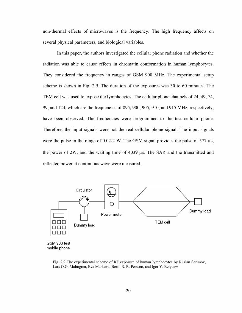
They considered the frequency in ranges of GSM 900 MHz. The experimental setup
scheme is shown in Fig. 2.9. The duration of the exposures was 30 to 60 minutes. The
TEM cell was used to expose the lymphocytes. The cellular phone channels of 24, 49, 74,
99, and 124, which are the frequencies of 895, 900, 905, 910, and 915 MHz, respectively,
have been observed. The frequencies were programmed to the test cellular phone.
Therefore, the input signals were not the real cellular phone signal. The input signals
were the pulse in the range of 0.02-2 W. The GSM signal provides the pulse of 577 µs,
the power of 2W, and the waiting time of 4039 µs. The SAR and the transmitted and
reflected power at continuous wave were measured.
Fig. 2.9 The experimental scheme of RF exposure of human lymphocytes by Ruslan Sarimov, Lars O.G. Malmgren, Eva Markova, Bertil R. R. Persson, and Igor Y. Belyaew

21
The results showed that all modulations of 2 W output power provided the SAR
of 5.4 mW/kg. In order to measure the changes of the chromatin conformation, the
authors used the anomalous viscosity time dependencies (AVTD) method. The results
suggested that the microwave radiation of the cellular phone affected chromatin
conformation in transformed lymphocytes.
The twelfth paper is the study of a method to investigate non-thermal effects of
radio frequency radiation on pharmaceuticals with relevance to RFID technology by
Felicia C.A.I. Cox, Vikas K. Sharma, Alexander M. Klibanov, Bae-Ian Wu, Jin A. Kong,
and Daniel W. Engels in 2006 [21]. They described the test setup of the experimental
method where they connected the TEM cell in series with a radiation source. They
controlled the temperature of the sample by using a combination of a fiber-optic
thermometer and thermo-electric cooler. Consequently, the sample temperature was
accurately controlled and maintained under conditions when the radio frequency radiation
(RFR) increased. The results showed that this methodology was an appropriate setup to
investigate the non-thermal effects of RFR for a range of incident power intensities,
frequencies, and initial sample temperature.
Experimental and numerical study of electromagnetic field influence on mollusk
neurons is presented by Z. Modebadze, B. Partcvania, T. Surguladze, and L.
Shoshiashvili in 2006 [22]. The authors have performed the experiment by placing
mollusk neurons inside the TEM cell to investigate the influence of EM radiation at 900
MHz. The activity of the mollusk neurons was observed. The authors have provided the
reasons of the experiment on the neurons that the neurons are well identified, and their
biophysical and electrophysiological characteristics are common to other animals.

22
Since the non-thermal effects were complex to do the experiment, and it required
the accurate estimation of exposure level and temperature control, the FDTD simulation
method was developed. This FDTD was designed for the RF radiation and RF power
absorption in complex environments including the models of living organisms. The
authors calculated the numerical study of SAR and temperature rise by using FDTD
method. The results showed that the electromagnetic field influenced on the neurons
habituation. From this paper, I have gained another idea of using the TEM cell for testing
the effects to animals.
The final paper researched in this study is that of mirror reflections in EMF
dosimetry, which was presented by Tomasz Dlugosz and Hubert Trzaske in 2007 [23].
The authors have pointed out that the measurement probe and the biological objects
under testing act as the secondary radiation source. The biological samples will absorb
the electromagnetic field and cause the field distribution. Consequently, the authors
proposed the formula for calibrating the probe antenna. The authors have also suggested
that before the experiment the testing devices which are used inside the TEM cell need to
be calibrated. They emphasize that probes and the biological test objects are able to cause
the error of the results, and influence to the accuracy of the results.
The references cited above cover a large variety of experiments using TEM cells.
Results from the studies cited served as a guideline for this research work.

23
Chapter 3: Theoretical Background 3.1 Transmission Lines
In this study, understanding of the transmission line theory is required. The TEM
cell is fed through a transmission line and one needs to have an understanding of the
reflection, transmission of the voltage and current wave on the feed line. A transmission
line can be defined in many ways. In general a transmission line is a medium that can be
transfer useful energy from one place to another. The transmission line, such as a wire, a
coaxial cable, or a waveguide, is used generally as the meaning of the material medium
or the structure path for transmitting the energy, such as the EM waves, the cellular
phone signals, or the radio signals. However, in this thesis, I would like to use the
definition of the transmission line, which is referred from the Microwave Engineer book
by David M. Pozar, which defines a transmission line as the distributed-parameter
network, where voltages and currents can vary in magnitude and phase over their length
[24].
Fig. 3.1 The transmission line schematics; (left) voltage and current definition, and (right) lumped-element equivalent circuit. This figure is from the Testing for Microwave Engineer book [24].

24
The schematics of a transmission line are shown in Fig. 3.1. The left schematic in
Fig. 3.1 shows a two-wire line as two conductors for the TEM wave propagation. This
can be drawn as a lumped-element circuit, as shown in the right schematic in Fig 3.1,
where R, whose unit is Ohm (Ω)/m, is the series resistance per unit length of both
conductors, L, whose unit is Henry (H)/m, is the series inductance per unit length of both
conductors. G, whose unit is Siemens (S)/m, is the shunt conductance per unit length, and
C, whose unit is Farads (F)/m, is the shunt capacitance per unit length. From the above
equivalent circuit, we can formulate the traveling wave voltage
zo
zo eVeVzV γγ −−+ +=)( (3.1.1)
the current of the wave propagation
zo
zo eIeIzI γγ −−+ +=)( (3.1.2)
and the complex propagation constant
))(( CjGLjRj ωωβαγ ++=+= (3.1.3)
where e-γz term indicates the wave propagation in the positive z direction, and eγz term
indicates the wave propagation in the negative z direction. α is the attenuation constant. β
is the phase constant. γ is the propagation constant. The characteristic impedance (Zo) of
the line is defined as
CjGLjRZo ω
ω++
= (3.1.4)
The wavelength on the line, which can be determined from the phase constant in
equation (3.1.3), is set as
βπλ 2
= (3.1.5)
25
and the phase velocity is set as
fv p λβω== (3.1.6)
where f is the frequency.
In general, when we are designing or simulating a transmission line, we assume
that the transmission line is ideal. This means that there is no loss effect. Therefore, the
loss of the line is very small and so can be neglected, by setting the resistance and
conductance to zero. This results in the fact that the attenuation constant (α) is zero.
Consequently, the characteristic impedance is set as
CLZo = (3.1.7)
The wavelength is
LCωπλ 2
= (3.1.8)
and the phase velocity is
LCv p
1= (3.1.9)
The transmission line is usually needed to be terminated with the load impedance
(ZL). In this case, the voltage reflection coefficient is considered. It is the amplitude of
the reflected voltage (Vo-), which is normalized by the amplitude of the incident voltage
(Vo+). It is given as
oL
oL
o
o
ZZZZ
VV
+−
==Γ +
−
(3.1.10)

26
The voltage standing wave ratio (VSWR) is a measure of the mismatch of a line.
VSWR is a real positive number. If it is equal one, the system has a matched load. It is
defined as
Γ−
Γ+=
1
1VSWR (3.1.11)

27
3.2 Waveguides
Since the TEM cell is one kind of waveguides, the theory of the waveguides is
also needed to understand the working of the cell. Waveguides are hollow tubes, such as
metal tubes, coaxial cables, or strand of glass fibers, used as a conductor or directional
transmitter for the electromagnetic waves. They are the EM feed line, and they are
commonly used in microwave communications, broadcasting, and radar installations.
There are two main types of the waveguide; a rectangular waveguide and a cylindrical
waveguide.
The dimensions of the waveguides are related to the wavelength. If the
dimensions are very large, the operating frequency will decreased. Therefore, to operate
properly, the waveguides need to have a certain minimum diameter relative to the
wavelength of the signal. If the waveguide is too narrow or the frequency is too low,
Fig. 3.2 Photograph of various rectangular waveguides

28
which means that the wavelength is too long, the EM fields are not able to propagate. In
the waveguide, the EM fields are propagating in various directions. There are two
common modes in the waveguide transverse-magnetic (TM) and transverse-electric (TE).
In TM mode, the magnetic lines of flux are perpendicular to the axis of the waveguide. In
TE mode, the electric lines of flux are perpendicular to the axis of the waveguide. At the
frequencies above the cutoff frequency, which is the lowest frequency at which the
waveguide is large enough, the waveguides will function well.
Since the TEM cell acts similar to the rectangular waveguide, a brief description
of the rectangular waveguide is described here. The rectangular waveguide, which is one
of the earliest transmission lines, is used to transport the microwave signal for many past
decades, and people still use it today. It is used for many purposes, such as couplers,
detectors, isolators, attenuators, and slotted lines. The operating frequencies of the
rectangular waveguide are from 1 GHz to over 220 GHz. Fig. 3.2 shows some of the
laboratory rectangular waveguide components that are available. The rectangular
waveguide can be used for high-power systems, millimeter wave systems, and in some
precision test applications.
The rectangular waveguide is able to propagate TE and TM modes, but not TEM
modes as the TEM cell, since only one conductor is present. The geometry of the
rectangular waveguide is shown in Fig. 3.3. We assume that the waveguide is filled with
a material of permittivity (ε) and permeability (µ). It is standard convention to have the
longest side of the waveguide along the x-axis, so that a is greater than b, where a is the
inside width, and b is the inside height.

29
TE modes
The TE modes are characterized when the Ez fields is zero, and Hz satisfies the
reduced wave equation of
0),(22
2
2
2
=⎟⎟⎠
⎞⎜⎜⎝
⎛+
∂∂
+∂∂ yxhk
yx zc (3.2.1)
From operating mathematic of (3.2.1), the cutoff frequency ( mncf ) is given by
22
21
⎟⎠⎞
⎜⎝⎛+⎟
⎠⎞
⎜⎝⎛=
bn
amf mnc
ππµεπ
(3.2.2)
where m is the number of half-wavelength variations of fields in the “a” direction, and n
is the number of the half-wavelength variations of fields in the “b” direction.
The dominant mode, which is the mode with the lowest cutoff frequency, is TE10
(m=1, n=0) because a is greater than b. Therefore, the lowest cutoff frequency is given as
µεa
fc 21
10 = (3.2.3)
Fig. 3.3 Geometry of the rectangular waveguide. This figure is from the Testing for Microwave Engineer book [24].
30
Many people misunderstand that TE00 mode is the dominant mode of the
rectangular waveguide, which is not correct. There is no TE00 for the rectangular
waveguide.
The wave impedance, which is able to determine from the transverse electric and
magnetic fields, is given as
βηk
HE
Zy
xTE == (3.2.4)
where εµη = is the intrinsic impedance of the material filling the waveguide. β,
which is the propagation constant, is given as
22222 ⎟
⎠⎞
⎜⎝⎛−⎟
⎠⎞
⎜⎝⎛−=−=
bn
amkkk c
ππβ (3.2.5)
µεω=k (3.2.6)
22
⎟⎠⎞
⎜⎝⎛+⎟
⎠⎞
⎜⎝⎛=
bn
amkc
ππ (3.2.7)
ZTE is real when β is real. It is the propagation mode. This means that if fc is less
than operating frequency (f), the modes will propagate. ZTE is imaginary when β is
imaginary. It is the evanescent mode. This means that the modes are evanescent modes if
fc is greater than f. All field components will decay exponentially away from the source
of excitation.
The guide wavelength is defined as the distance between two equal phase planes
along the waveguide, and is given as
βπλ 2
=g (3.2.8)
31
The phase velocity is
βω
=v (3.2.9)
TM modes
The TM modes are characterized when the Hz fields is zero, and Ez satisfies the
reduced wave equation of
0),(22
2
2
2
=⎟⎟⎠
⎞⎜⎜⎝
⎛+
∂∂
+∂∂ yxek
yx zc (3.2.10)
The propagation constant of the TM modes is the same as that of the TE modes.
The cutoff frequency for the TMmn modes is also the same as that of the TEmn modes.
However, the dominant mode is the TM11 mode. The guide wavelength and phase
velocity for TM modes are also the same as those for TE modes.
There are no TM00, TM01, or TM10 modes. The lowest order TM mode to
propagate, which is lowest cutoff frequency, is the TM11 mode. The cutoff frequency
( 11cf ) is given as
22
11 21
⎟⎠⎞
⎜⎝⎛+⎟
⎠⎞
⎜⎝⎛=
bafc
ππµεπ
(3.2.11)
The first cutoff frequency ( 11cf ) of the TM mode is larger than the first cutoff
frequency of the TE mode ( 10cf ).
The wave impedance, which is able to determine from the transverse electric and
magnetic fields, is given as
kH
EZ
y
xTM
βη== (3.2.12)
32
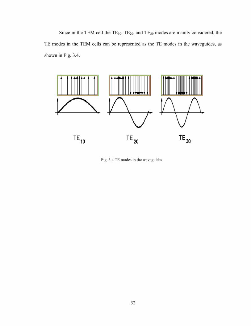
Since in the TEM cell the TE10, TE20, and TE30 modes are mainly considered, the
TE modes in the TEM cells can be represented as the TE modes in the waveguides, as
shown in Fig. 3.4.
Fig. 3.4 TE modes in the waveguides

33
3.3 Mode Excitation
Since in this study probes were inserted in the TEM cell for field measurements
etc, this section would provide the basic information for the determination of the
excitation and input impedance of the probes. When the electric or magnetic current
source, such as a monopole antenna, is inserted in the waveguide, first we need to
consider the electric current source ( J ), whose location is between two transverse planes
at z1 and z2, as shown in Fig. 3.5. The +E , and +H fields are then generated. As we can
see in Fig. 3.5, the +E , and +H fields are traveling in the +z direction, and the −E , and
−H fields are traveling in the –z direction. The E and H fields can be formulated in terms
of the waveguide modes as given below [24]
( ) ,ˆ zj
nznnn
nnn
neezeAEAE β−++++ ∑∑ +== z > z2, (3.3.1)
( ) ,ˆ zj
nznnn
nnn
nehzhAHAH β−++++ ∑∑ +== z > z2, (3.3.2)
( ) ,ˆ zj
nznnn
nnn
neezeAEAE β∑∑ −== −−−− z < z1, (3.3.3)
( ) ,ˆ zj
nznnn
nnn
nehzhAHAH β∑∑ +−== −−−− z < z1, (3.3.4)
Fig. 3.5 The arbitrary electric or magnetic current source in wavelengths. This figure is from the Testing for Microwave Engineer book [24].
34
where n represented the TE or TM modes. To determine the unknown amplitude (An+),
the current source ( J ) is given, then by using the Lorentz reciprocity theorem
with 021 == MM ,
( ) ( )∫∫ ⋅−⋅=⋅×−×VS
dvJEJEsdHEHE 21121221 (3.3.5)
where S is the closed surface, which enclose the volume (V), and iE , iH are the fields
due to the current source iJ when i is equal to 1 or 2.
By fixing the volume (V) to be the region between the waveguide walls and the
transverse cross-section planes (z), the amplitude of the positive traveling waves can be
derived as
( ) dveJezeP
dvJEP
A zj
V znnVn
nn
nnβ⋅−
−=⋅
−= ∫∫ −+ ˆ11 (3.3.6)
∫ ⋅×=0
ˆ2S nnn dszheP (3.3.7)
where Pn is the normalization constant proportional to the power flow of the nth mode.
Also, the amplitude of the negative traveling waves can be derive as
( ) dveJezeP
dvJEP
A zj
V znnVn
nn
nnβ−+− ⋅+
−=⋅
−= ∫∫ ˆ11 (3.3.8)
The above equations can be used generally for any type of waveguide, where
modal fields can be defined.

35
3.4 Transverse Electromagnetic Cell or TEM Cell
The term ‘TEM cell’ has been used many times, so a close examination of the
TEM cell is necessary at this point. The transverse electromagnetic transmission cell,
which is the acronym for the TEM cell, was first introduced by Myron L. Crawford at the
National Bureau of Standards in 1973 [9]. Crawford realized that the electronic or
electromechanical systems in the open systems would affect the level and number of
potential interfering signals. For this reason, he presented the TEM cell for establishing
uniform electromagnetic fields in a shielded environment [6]. It operated at broad band
frequency, which was restricted by the waveguide multimode frequency associated with
the cell size.
It was developed from the coaxial line. The TEM cell propagates the TEM wave.
It is widely used for radiated immunity and emission testing of electronic devices and
exposing biological objects to electromagnetic radiation. The TEM cell consists of a
rectangular coaxial transmission section which is tapered with the coaxial connectors of
both sides, as shown in Fig. 3.6. The inner conductor, which is called the septum, acts as
Fig. 3.6 The rectangular TEM cell

36
the positive conductor or the hot line. The outer conductor acts as the ground. The
impedance along the TEM cell is 50 ohms. Therefore, a matched 50 ohms is terminated
at the output port. The area under test of the TEM cell is one-third of volume between the
septum and the outer wall. The characteristic impedance, the first cutoff frequency, and
the first resonant frequency equations were presented by M. Crawford [7]. The
characteristic impedance (Zo) of the TEM cell is given as
o
o Cbg
ba
Z
επ
π∆
−⎥⎦
⎤⎢⎣
⎡⎟⎠⎞
⎜⎝⎛−
=
2sinhln24
1 (3.4.1)
where a is the TEM cell’s width, b is the TEM cell’s height, and g is the gap between the
septum and the outer conductor. These parameters are the length of the TEM cell
dimension in meter, as shown in Fig. 3.7. ∆C is the fringe capacitance between the edges
of the center plate and the sidewalls of the TEM cell. If the ration of a and b is larger than
1, ba > 1, we can then ignore the term of oC ε∆ .
Fig. 3.7 Cross section view of the TEM cell

37
The cutoff frequency ( cf ) of the TEM cell is given as
( ) 2222
2namb
abcTEf mnc += (3.4.2)
Since the dominant mode the TEM cell is TE10, which is the same as that of the
rectangular waveguide, the first cutoff frequency of the TEM cell is given as
( )acTEfc 210 = (3.4.3)
where c is the velocity of light.
The resonant frequency ( resf ) of the TEM cell is given as
( )2
2
2 ⎟⎟⎠
⎞⎜⎜⎝
⎛+=
mnmncmnpres l
pcfTEf (3.4.4)
where lmn is the resonant length of the TEM cell, and p is the particular waveguide mode.
The first resonant frequency of the TEM cell, which p is equal to 1, is given as
( )2
210101 2 ⎟⎟
⎠
⎞⎜⎜⎝
⎛+=
mncres l
cfTEf (3.4.5)
The electric field of the areas under test, which is the midway between the septum
and outer walls, is given as [12]
]/)(4cos[)'(2)12(221222
)12212(1)'(
clfLlleinSkkinSkinS
inPoZkkinSkinS
bllE
πφα ++−−++
++==+ (3.4.6)
where lL
lL
in ee
S α
α
2
2
11
−
−
Γ−
Γ+= (3.4.7)
)'(41 1 llek +−= α (3.4.8)

38
)'(42 1 llek ++= α (3.4.9)
)2
(tan 2221
oLL
oLL ZXR
ZX−+
= −φ (3.4.10)
where 'l is the length of observed position, Pin is the net power, which flows in the TEM
cell, and ZL = RL+jXL is the terminal load impedance.
Fig. 3.8 shows the ideal field strengths for varying heights above and below the
septum. At each corresponding levels both above and below septum the same results for
Fig. 3.8 The ideal field strength plots with various heights above and below the septum

39
field strengths are due to the symmetric nature of the system. In addition, if the positions
on both side walls (left and right) are the same, the electric field strength should be same
due to symmetry. The level 1 is the furthest from the septum, so the electric field strength
is less. The level 2 is the middle level between the level 1 and 3. The level 3 is the nearest
to the septum, so the electric field is the highest strength. Therefore, if it is higher level,
the electric field is stronger.
The H field is equal to the E field value divided by 377 ohms. Thus the H field
determination relies on the relationship between E and H for free-space propagation. The
VSWR for the TEM mode propagation through the TEM cell should be less than 1.2.
The objects under test should be placed on the rectangular transmission section between
the top or bottom septum and the outer conductor. The size of the objects should relate to
the test volume inside the TEM cell. If the object is not small, the RF field inside the cell
is essentially shorted out in certain locations, causing a higher intensity of field strengths
and field distribution in the TEM cell. The advantages of the TEM cell are small size, low
cost, and the need for a high power amplifier is not necessary. It is also portable, people
can carry it anywhere.

40
3.5 Monopole Antenna
In this thesis, a monopole probe was used to measure the electric field. Therefore,
some of the basic concepts behind the working of this instrument need to be introduced.
A monopole antenna acts as one half of a dipole antenna with a ground plane. With the
large ground plane, the monopole antenna will be able to behave like the dipole antenna.
To select the length of the antenna, this equation is needed
λfv = (3.5.1)
then 4λλ =monopole (3.5.2)
The monopoleλ is the length of the monopole. The measured results in voltage are
also needed to be converted to electric fields. To do this, one first needs to determine the
antenna factor using the following formula [28]
dBGfK dB 8.29log20 −−= (3.5.3)
where K is the antenna factor, f is the frequency in MHz, and GdB is antenna gain. The
antenna gain of the monopole is 3.09 dB, which is the same value as the dipole antenna
due to the ground effect of the TEM cell.
Finally, the electric field is the sum of the adjusted spectrum analyzer reading and the
antenna factor. The expression is given as
(K)Factor Antenna +Result ReadingAnalyzer = E (3.5.4)
The electric field probe is capable of providing reasonably accurate measurements
of E-fields. The probe is capable of measuring the electric field radiation on cables and
within circuits.

41
The electric field probe can be built easily, using configuration as shown in Fig.
3.9. It is low cost and is of good quality. The materials used for construction was used
from materials found in the laboratory. It is made of two parts; a 50-ohms BNC connector
and a coaxial cable. The construction procedure is detailed in the next chapter.
A double-ended monopole antenna was also used in the study. The double-ended
monopole antenna was attached at the top of the outer conductor. The antenna acted as
the signal leader, which was induced in the free space outside the TEM cell. The length
of the double-ended antenna was calculated from the equation (3.5.1) and (3.5.2).
Fig. 3.9 The construction of the electric field probe. This figure is from the Testing for EMC Compliance book [26].

42
3.6 Magnetic Field Probe
Magnetic field measurements were also done in this study using a magnetic loop
probe. The magnetic loop is useful for many kinds of measurements including: measuring
voltage drop across conductors and planes, current flowing in conductors and magnetic
fields as well. The magnetic field probe is usually shielded. The unshielded loop probe is
sensitive to both types of fields: magnetic and electric. The resulting voltage from the
probe is not very accurate. Therefore, the shielded probe prevents the pickup of stray
electric fields that will produce incorrect data. Generally, common-mode currents are
radiated from cable assemblies that contain a defective shield. These defective shields
cause the majority of radiated emissions.
Fig. 3.10 The construction of the magnetic loop probe. This figure is from the Testing for EMC Compliance book [26].

43
The shielded magnetic loop is made from semi-rigid coaxial cable as shown in
Fig. 3.10 [26]. The loop is formed by making a circle or square from the semi-rigid coax
with a gap placed symmetrically in the middle of the loop. The position of the gap is very
important for the performance of the shield. If the gap is not in the middle of the loop,
shielding effectiveness is compromised. All loop probes are directional. Therefore, when
searching for sources of emissions, the probe should be positioned in two or three
orientations to locate the strongest signal. Fig. 3.11 shows the magnetic probe model that
was used to build my magnetic probe. The construction procedure will be described in
the next chapter.
The magnetic field can be obtained from the following equation [29],
AV
H probe
µω= (3.6.1)
where H is the magnetic field, Vprobe is the measured voltage by using the loop probe, A
is the loop area, ω is the angular frequency, and µ is the permeability of the loop probe.
Fig. 3.11 The magnetic loop probe model. This figure is from the Testing for EMC Compliance book [26].

44
Chapter 4: Simulation and Experimental Configurations
4.1 Simulation Configuration
4.1.1 TEM Cell Characteristics
The simulation study of the TEM cell was carried out by using the Computer
Simulation Technology (CST) Microwave Studio software [27]. This software is a fully
featured software package for electromagnetic analysis and design in the microwave
frequency range. The structure can be easily designed by using solid modeling front-end
function which is based on ACIS modeling kernel.
Fig. 4.1 The parameters of the TEM cell dimension

45
The TEM cell parameters were obtained by using the equation (3.4.1), and (3.4.3).
All input parameters for simulation are shown in Fig. 4.1. The material of the TEM cell is
assumed to be a perfect electric conductor (PEC). The TEM cell is designed in the
horizontal direction, which means the electric field vector is oriented in the y-direction,
and the electromagnetic wave propagates to z-direction as shown in Fig. 4.2.
To apply the input signal port into opened-end, a discrete port was used. The port
was connected between the outer shield and the septum, as shown in Fig. 4.3 (left). The
50-ohms impedance load was terminated at another end of the TEM cell between the
outer shield and the septum, as shown in Fig 4.3 (right).
Fig. 4.2 The CST model of the TEM cell: outside view (above), and inside view (bottom)

46
Also, for the excitation signal a Gaussian pulse was applied at the discrete port.
Fig. 4.4 shows the boundary condition of the simulation, which was defined as open
space condition. This simulation setup would provide the results of electromagnetic
fields, characteristic impedance, and VSWR.
Fig. 4.3 Input signal port (left), and 50-ohms impedance load (right)
Fig. 4.4 Boundary condition

47
4.1.2 Simulation Setup of Cellular Phone Measurement
For this simulation, the double-end monopole antenna was designed. It was
attached to the outer conductor, as shown in Fig. 4.5. The lengths of the double-ended
monopole antenna h1 = h2 = 9.4 cm a diameter of 0.2 cm.
The discrete port was used to provide the cellular phone signal. The port was
attached with the outer shield as shown in Fig. 4.6. The 50-ohms impedance loads were
terminated at both ends of the TEM cell. This simulation setup is expected to produce the
electromagnetic fields and VSWR for the experimental design.
Fig. 4.5 The double-ended monopole antenna is attached to the outer conductor.
Fig. 4.6 The signal leader was attached with the outer conductor of the TEM cell.

48
4.1.3 Simulations to Improve Electric Field Uniformity
To improve the uniform electric field, there are two options. Either the length of
the signal leader could be reduced or one could build a smaller TEM cell. In this research
both these options were studied. For the first simulation the length of signal leader was
reduced to 1 cm. The second simulation was the simulation of the smaller TEM cell. The
dimension parameters of the TEM cell are shown in Fig. 4.7.
Fig. 4.7 The smaller TEM cell dimensions

49
4.2 Experiments
4.2.1 Construction of TEM Cell
In order to measure the EM radiation from a cellular phone and to protect against
signal interference a shielded environment is necessary. The TEM cell can provide such
an environment while generating a uniform electric field. The dimensions of the
laboratory constructed TEM cell is shown in Fig. 4.1. The septum was designed and
fabricated first, as shown in Fig. 4.8.
Fig. 4.9 shows both tapered sections of the TEM cell, which were fabricated
secondly.
Fig. 4.8 The constructed septum (left); The septum dimensions (right)
Fig. 4.9 The constructed tappered section parts (left); The tapered section part dimensions (right)

50
The rectangular transmission section was then created, as shown in Fig. 4.10.
Finally, all the parts were assembled together as the completed TEM cell shown in Fig.
4.11.
Fig. 4.10 The constructed rectangular transmission section part (left); The rectangular transmission section part dimensions (right)
Fig. 4.11 The completed TEM cell

51
4.2.2 Construction of Electric Field Probe
The electric field probe was designed and constructed next, as described here. The
50-ohms impedance coaxial cable was used to fabricate this probe where a portion of the
shield was peeled and the insulation the center conductor was left the way it is. Then, a
small piece of shrinkable tubing was added over the end to stabilize the shield and
insulated the probe from accidental contact with electronic circuitry, as shown in Fig.
4.12.
Fig. 4.12 The electric field probe components by Scott Roleson [30]
Fig. 4.13 The laboratory constructed electric field probe

52
At the other end of the coaxial cable, an N-typed connector was added, as shown
in Fig. 4.13.
4.2.3 Construction of Magnetic Field Probe
The magnetic field probe is required to measure the magnetic field. In this study,
the magnetic field was built with low cost and with high quality. The magnetic field
probe was built from paper clip or rigid wire. In addition to measuring the voltage in
circuits, the paper clip probe can also be used to measure the relative phase or time delay
between two signals.
The material needed include a BNC connector to mount for the loop, a paper clip
and the rubber insulator. The first step was covering the insulator to the paper clip, as
shown in Fig 4.14.
Then, the paper clip was bent to form a circular loop. The next step was installing
the paper clip to the BNC connector. Finally, the layer of the insulator was shielded. The
completed magnetic probe is shown in Fig. 4.15. This magnetic probe was constructed in
a short time and was simple to build from the available parts in the laboratory. It is very
useful and a real advantage when time is a factor in the investigative study.
Fig. 4.14 Covering the paper clip with the insulator. This figure is from the Testing for EMC Compliance book [26]
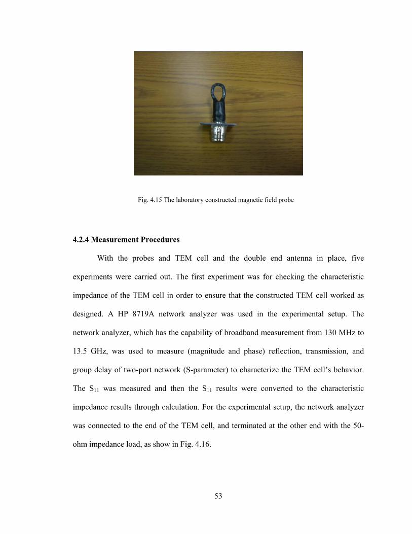
53
4.2.4 Measurement Procedures
With the probes and TEM cell and the double end antenna in place, five
experiments were carried out. The first experiment was for checking the characteristic
impedance of the TEM cell in order to ensure that the constructed TEM cell worked as
designed. A HP 8719A network analyzer was used in the experimental setup. The
network analyzer, which has the capability of broadband measurement from 130 MHz to
13.5 GHz, was used to measure (magnitude and phase) reflection, transmission, and
group delay of two-port network (S-parameter) to characterize the TEM cell’s behavior.
The S11 was measured and then the S11 results were converted to the characteristic
impedance results through calculation. For the experimental setup, the network analyzer
was connected to the end of the TEM cell, and terminated at the other end with the 50-
ohm impedance load, as show in Fig. 4.16.
Fig. 4.15 The laboratory constructed magnetic field probe

54
The second experiment was the VSWR measurement. The HP 8719A network
analyzer is also needed for this experiment. The experimental setup is shown in Fig. 4.16.
The third experiment was designed to characterize the electric field of the TEM
cell. An E7402A spectrum analyzer was used by connecting to the electric field probe.
The electric field was measured on the yz plane in the rectangular section. The fields were
measured at positions around a 7 by 3 matrix as shown in Fig. 4.17 through the top of the
outer conductor plate. The experimental setup is shown in Fig. 4.18.
TEM cell HP 8719A Network Analyzer
50-ohms Load
Fig. 4.16 The experimental setup of characterizing the TEM cell’s impedance

55
In the fourth and fifth experiments, a cellular phone was used as a signal
generator. The experimental setup consisted of a double-ended monopole antenna
Fig. 4.17 The observation points on the top of the TEM cell
Fig. 4.18 The experimental setup of the electric field distribution measurement
Attached electric field probe to the outer shield
Spectrum analyzer
50-ohms load
Connected to signal generator

56
attached to the top of the TEM cell’s outer conductor as a signal leader that provided a
near-field environment inside the TEM cell. Once the channel in the range of 800 - 915
MHz between the cellular phone and the base stations was established, the signals could
propagate between the free space outside and inside the TEM cell through the double-
ended monopole antenna.
The experimental setup is shown in Fig. 4.19. The cellular phone tested was an
AT&T Motorola C139. The lengths of the double-ended monopole antenna h1 = h2 = 9.4
cm with the diameter of 0.2 cm. The length of the double-ended monopole antenna (h1 +
h2) was chosen in accordance with a half-wave length associated with the operating
frequency of the cellular phone at 825.125 MHz for optimum signal transreceiving, i.e.,
receiving at the external monopole and transmitting at the internal monopole or vice
versa.
Fig. 4.19 Experimental setup for the cellular phone near-field EM exposure using the laboratory constructed TEM cell.

57
The objective of both these experiments were to experimentally determine the
best setup for the TEM cell that can be used as a near-field exposure box for radiation
effects on biological cells studies. The criteria to be considered are the coupling voltage
obtained at the TEM cell ports and the field distribution within the usable area under test
(AUT), both of which are studied as functions of cellular phone position, polarization,
and dialing type.
(a)
(b)
(c)
Fig. 4.20 Positions and directions of the cellular phone: (a) locating the cellular phone at level A outside the TEM cell and placing the cellular phone in X, Y, Z directions, (b) attaching the cellular phone with the outer conductor inside the TEM cell and placing the cellular phone in X, Y, Z directions, and (c) locating the cellular phone on the top of the inner conductor inside the TEM cell and placing the cellular phone in X, Y, Z directions.

58
The forth experiment was for coupled voltage measurement. The coupled voltage
amplitude were measured at the TEM cell ports (P1 and P2) while establishing a call.
Here the variables are the cellular phone polarization (X, Y, and Z), and the location of the
cellular phone, as indicated in Fig. 4.19, by labels A (external surface), B (internal
surface), and C (on the septum), and the dialing type (in and out). Fig. 4.20 shows placing
of the cellular phone in 3 levels and 3 directions during the experiments. The fifth
experiment was designed to examine the field distribution within the AUT. The Agilent
E7402A spectrum analyzer was used in association with the 9.4 cm double-ended
monopole antenna by using a probe to monitor the electric field on the yz plane in the
rectangular section. The field observation positions are arranged in a 7 by 3 matrix as
shown in Fig. 4.17 through the top of the outer conductor plate. The center position was
reserved for attaching the double-ended monopole antenna.
4.2.5 Improvement of Electric Field Uniformity
As mentioned previously, to improve the field uniformity, there are two options.
First, we can decrease the length of the signal leader as to reduce an obstacle size inside
the TEM cell. For this experimental, the 1 cm signal leader referenced to the original
signal leader was built and the fifth experiment in the section 4.2.5 was repeated. Another
attempt to further improve the uniformity of the field distribution was by using a smaller
TEM cell, as shown in Fig. 4.21. An AT&T Nokia 7210 was used as the testing cellular
phone for GSM 1800. The smaller TEM cell was assembled with parameters, as shown in
Fig. 4.7. In this case, the cellular phone establishes the channel at 1800 MHz. The length
of the signal leader is 5 cm, corresponding to the half-wave length of the cellular phone’s

59
frequency. The cell impedance from measurement is 50.84 ohms and the first resonant
frequency is 1.54 GHz.
Fig. 4.21 The laboratory constructed smaller TEM cell

60
Chapter 5: Simulation and Experimental Results
In this chapter the results from simulation for the TEM cell design and the
experimental results from the configuration described earlier are presented and discussed.
Results from simulation using the FIT code are discussed first.
5.1 Simulation Results
5.1.1 Characterizing the TEM Cell
Fig. 5.1 shows the time domain reflectometer (TDR) result. The TDR result
represents the characteristic impedance of the TEM cell. The impedance characteristic of
Fig. 5.1 TDR result represented the characteristic impedance of the TEM cell

61
the TEM cell is 50.8427Ω. The result also shows two peaks, due to reflection. The
reflection positions are obtained from the equation,
λfv = (5.1.1)
Since we know that v is the velocity of the signal travelling inside the TEM cell, which is
equal to 8103× m/s. Then, we know the time from the result. Finally, we can calculate for
the distance. So, we can determine the reflection position. The first peak is the reflection
of the tappered section. It is on the input port side or close to the discrete port. The
second peak is the reflection of the rectangular transmission section. It is on the other end
of the TEM cell or far from the discrete port.
Fig. 5.2 VSWR result of the TEM cell

62
Fig. 5.2 shows the VSWR result. The result shows the VSWR of 1.2 before the
first resonant frequency. The result indicates that the first resonant frequency is 545
MHz. The second resonant frequency is 654 MHz. The third resonant frequency is 786
MHz. The forth resonant frequency is 913 MHz.
According to the calculated results, the first resonant frequency, which is the TE10
mode, is 515.11 MHz. The second resonant frequency, which is the TE11 mode, is 654.92
MHz. The third resonant frequency, which is the TE21 mode, is 793.86 MHz. The forth
resonant frequency, which is the TE30 mode, is 909.69 MHz. They are obtained by using
equation (3.3.4),
( )2
2
2 ⎟⎟⎠
⎞⎜⎜⎝
⎛+=
mnmncmnpres l
pcfTEf (5.1.2)
A comparison of the simulated and calculated results shows that they are good
agreement.
Fig. 5.3 Cross view of the electric field contour inside the TEM cell at 100 MHz

63
Fig. 5.3 shows the cross view of the electric field contour inside the TEM cell,
which is simulated at 100 MHz. A close look and approximate calculation from the
contour shows a uniform electric field in about one-third of the TEM cell’s volume. This
is in agreement with the results presented in Crawford’s paper [9].
A close analysis of Figs. 5.1 to 5.3 suggest that the design of the TEM cell is in
agreement with the theory presented earlier, that is the VSWR should be about 1.2 and
the areas under test or the uniformity areas is one-third of the TEM cell volume. This
suggests that the TEM cell has been designed to industry standards
5.1.2 Cellular Phone Radiation
Fig. 5.4 shows the VSWR result of the TEM cell with the 9.4 cm double-ended
monopole antenna attached.
Fig. 5.4 VSWR result of the TEM cell with the 9.4 cm double-ended monopole antenna

64
The result shows a higher value of VSWR when the signal leader is attached
inside the TEM cell. The first resonant frequency is moved up to 505 MHz. The third
resonant frequency is shifted to 800 MHz. There is also a ripple at 340 MHz. It is
principally because the TEM cell is excited by the signal leader with the TE10 mode at the
center, the major contribution of the radiation field is from the TE30l resonant fields
where l is the cell’s effective length due to the tapered sections.
Fig. 5.5 shows the top view of the normalized electric field distribution from
simulation, which is assumed that the cellular phone is dialling from the outside the TEM
Fig. 5.5 (Top) configuration of the TEM cell and the signal leader used in the simulation. (Bottom) top view of normalized resulting electric field distribution when the cellular phone is dialling.

65
cell. Here the field distribution was normalized by using the same factors from
measurement results when establishing with calling-in and out signals and cellular phone
located outside the TEM cell. This will be discussed further in the experimental result
section. The cellular phone’s incoming and outgoing signals are generated using the
lumped excitation source (825.125 MHz) attached to the external end of the signal leader.
5.1.3 Improvement of Electric Field Uniformity
As mentioned in the previous chapter, there are two ways to improve the uniform
electric field. One method is to shorten the length of the antenna. Fig. 5.6 shows the
VSWR of the TEM cell attaching with the shorter double-ended monopole antenna,
which is 1 cm in length.
Fig. 5.6 VSWR result of the TEM cell with the 1 cm double-ended monopole antenna

66
The result shows that the VSWR of the TEM cell with the 1 cm signal leader is
lower than that of the 9.4 cm signal leader. There is no ripple and no shifting of the
modes. This VSWR result is vey closed to the VSWR of the original TEM cell, which is
without the signal leader. It is, however, a bit higher than the original TEM cell, and the
bandwidth is also wider mainly due to interaction with the wave reflected from the signal
leader.
Fig. 5.7 shows the electric fields from simulation with the shorter signal leader at
825.125 MHz. The field distribution is normalize by using the same factors from
measurement results when establishing with calling-in and out signals and cellular phone
located outside the TEM cell. The contour indicates that the electric field is more
uniformity. This means that the shorter signal leader can improve the size of the AUT.
Fig. 5.7 Top view of simulated electric field distributions of the 1-cm signal leader as referenced to the 9.4 cm signal leader.

67
However, comparing the contours of Figs. 5.5 to 5.7, the shorter signal leader provides
the less field strength.
Another attempt to further improve the uniformity of the field distribution is using
the smaller TEM cell. The smaller TEM cell was assembled with parameters, as shown in
Fig. 4.7. An AT&T Nokia 7210 was used as the testing cellular phone for GSM 1800. In
this case, the cellular phone frequency at 1800 MHz was established for the experiment.
The length of the signal leader is 5 cm, corresponding to the half-wave length of the
cellular phone’s frequency. The cell impedance from measurement is 50.84 ohms and the
first resonant frequency is 1.54 GHz. With the smaller TEM cell, the length of the signal
leader no longer induces the higher order modes as it can be shown by the VSWR shown
in Fig. 5.8. This is mainly because the operating frequency is no longer affected by the
higher modes. The usable area is, however, reduced as a trade-off. The inset is the
uniform electric field distribution inside the smaller TEM cell.
Fig. 5.8 Simulated results of the VSWR (bottom), and the electric field distribution (above) of the smaller TEM cell.

68
5.1.4 The Magnetic Field
The magnetic field inside the TEM cell was also simulated for analysis. The
simulation software is the same used for E-field analysis. The top view of the magnetic
fields in Y direction at 500 MHz was measured 2 cm above the septum, shown in Fig.
5.9. The contour shows the pecks at the both side of the plane, and the uniform magnetic
field at the center.
Fig. 5.9 The top view simulation of the magnetic field in Y direction at 500 MHz of the smaller TEM cell at 2 cm above the septum.

69
5.2 Experimental Results
5.2.1 Characterizing the TEM Cell
Fig. 5.10 shows the characteristic impedance of the TEM cell. The experimental
setup is shown in Fig. 4.16. The S11 results were corrected by using the HP 8719A
network analyzer. The S11 results were then converted to the characteristic impedance
results, as represented in TDR plot, by using a MATLAB code in the appendix B.
Fig. 5.11 shows the VSWR result of the TEM cell. The experimental setup is also
shown in Fig. 4.16. The VSWR result was obtained by using the HP 8719A network
analyzer. The result shows the VSWR of 1 before the first resonant frequency.
Fig. 5.10 Characteristic impedance results of the TEM cell.

70
Fig. 5.12 shows the results of the electric field at 100 MHz. The experimental
setup is shown in Fig. 4.18. The input power is 60 W. It is measured 2 cm above the
septum. The results show the uniform electric field in yz plane. This can be represented
by Fig. 5.13.
Fig. 5.11 Experimental VSWR result of the TEM cell.

71
Fig. 5.12 Experimental results of the electrical field at 100 MHz and 2 cm above the septum
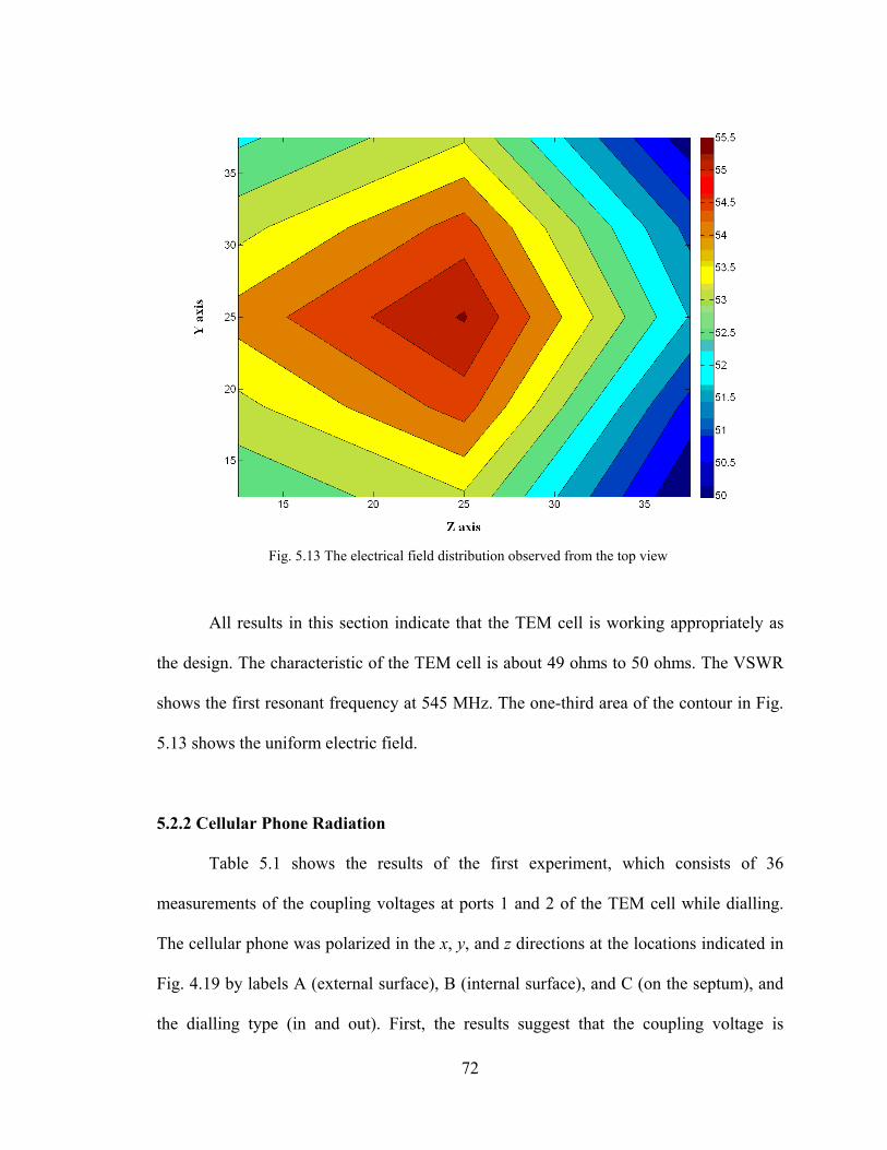
72
All results in this section indicate that the TEM cell is working appropriately as
the design. The characteristic of the TEM cell is about 49 ohms to 50 ohms. The VSWR
shows the first resonant frequency at 545 MHz. The one-third area of the contour in Fig.
5.13 shows the uniform electric field.
5.2.2 Cellular Phone Radiation
Table 5.1 shows the results of the first experiment, which consists of 36
measurements of the coupling voltages at ports 1 and 2 of the TEM cell while dialling.
The cellular phone was polarized in the x, y, and z directions at the locations indicated in
Fig. 4.19 by labels A (external surface), B (internal surface), and C (on the septum), and
the dialling type (in and out). First, the results suggest that the coupling voltage is
Fig. 5.13 The electrical field distribution observed from the top view
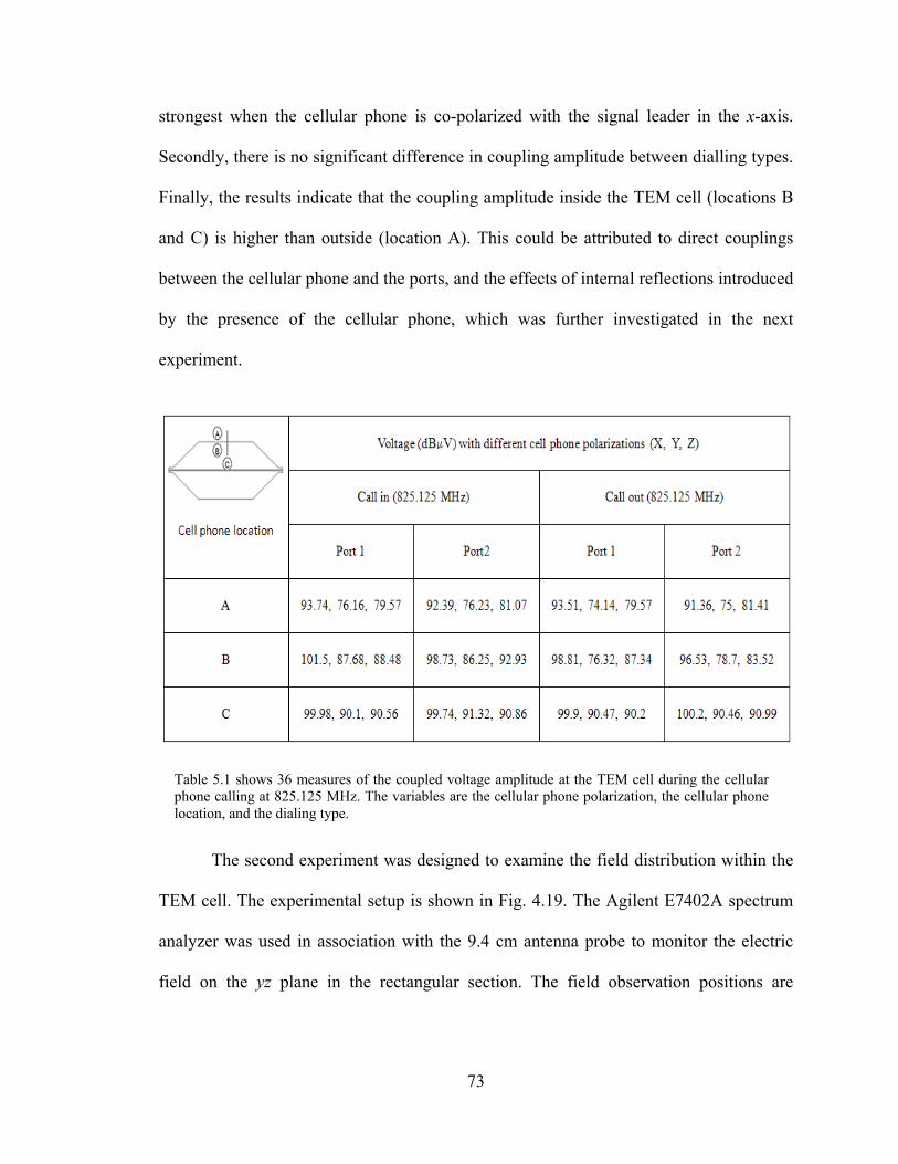
73
strongest when the cellular phone is co-polarized with the signal leader in the x-axis.
Secondly, there is no significant difference in coupling amplitude between dialling types.
Finally, the results indicate that the coupling amplitude inside the TEM cell (locations B
and C) is higher than outside (location A). This could be attributed to direct couplings
between the cellular phone and the ports, and the effects of internal reflections introduced
by the presence of the cellular phone, which was further investigated in the next
experiment.
The second experiment was designed to examine the field distribution within the
TEM cell. The experimental setup is shown in Fig. 4.19. The Agilent E7402A spectrum
analyzer was used in association with the 9.4 cm antenna probe to monitor the electric
field on the yz plane in the rectangular section. The field observation positions are
Table 5.1 shows 36 measures of the coupled voltage amplitude at the TEM cell during the cellular phone calling at 825.125 MHz. The variables are the cellular phone polarization, the cellular phone location, and the dialing type.

74
arranged in a 7 by 3 matrix as shown in Fig. 4.17 through the top of the outer conductor
plate. The center position was reserved for attaching the signal leader.
Fig. 5.14 Each cell phone’s position in experiment and the electric field results. The arrow’s pointing out the cell phone represents calling out, and the arrow’s pointing to the cell phone represents calling in. The electric field results were measured at 3.5 cm from the outer conductor.

75
The contour plots of the electric field distribution at 825.125 MHz on the
observation plane with the testing cellular phone aligned in the x-axis, corresponding to
the strongest coupling, are shown in Fig. 5.15.
The amplitudes of the fields are normalized by the field amplitude at the plane
center. The profiles in Figs. 5.15(a), 5.15(b), and 5.15(c) are associated with the cellular
phone locations A, B, and C, respectively, in accordance with the calling-in signal.
Similarly, Figs. 5.15(d), 5.15(e), and 5.15(f) are the contours associated with the
locations A, B, and C, respectively, during the phone is calling out. As expected, the field
distribution is more uniform when the cellular phone is establishing a call outside the
Fig. 5.15 Profiles of the normalized electric field distribution at 825.125 MHz on the yz plane during establishing with calling-in and out signals at different cellular phone locations. (a) location A, calling-in signal, (b) location B, calling-in signal, (c) location C, calling-in signal, (d) location A, calling-out signal, (e) location B, calling-out signal, and (f) location C, calling-out signal.

76
TEM cell. The field amplitude when dialling outside [Figs. 5.15(a) and 5.15(d)] gradually
changes at the rate of 2% compared with 5% unpredictably abrupt changes when dialling
inside at location B on the ceiling [Figs. 5.15(b) and 5.15(e)].
Even though, more steadily change can be observed when the cellular phone is
moved further from the ceiling at location B to the septum at location C [Figs. 5.15(c)
and 5.15(f)], the field fluctuation caused by the presence of the cellular phone inside the
TEM cell evidently reduces the usable size of the AUT.
The best setup is achievable with the phone located at A and aligned in the x-axis.
It can be noted from the profiles shown in Figs. 5.15(a) and 5.15(d) that, even though the
TEM cell is excited by the signal leader with the TE10 mode at the center, the major
contribution of the radiation field is from the TE30l resonant fields where l is the cell’s
effective length due to the tapered sections.
Fig. 5.16 VSWR measurement of the TEM cell with the 9.4 cm signal leader and TEM cell ports connected to the network analyzer.
|
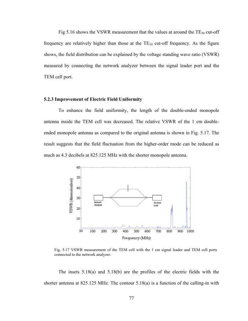
77
Fig 5.16 shows the VSWR measurement that the values at around the TE30 cut-off
frequency are relatively higher than those at the TE10 cut-off frequency. As the figure
shows, the field distribution can be explained by the voltage standing wave ratio (VSWR)
measured by connecting the network analyzer between the signal leader port and the
TEM cell port.
5.2.3 Improvement of Electric Field Uniformity
To enhance the field uniformity, the length of the double-ended monopole
antenna inside the TEM cell was decreased. The relative VSWR of the 1 cm double-
ended monopole antenna as compared to the original antenna is shown in Fig. 5.17. The
result suggests that the field fluctuation from the higher-order mode can be reduced as
much as 4.3 decibels at 825.125 MHz with the shorter monopole antenna.
The insets 5.18(a) and 5.18(b) are the profiles of the electric fields with the
shorter antenna at 825.125 MHz. The contour 5.18(a) is a function of the calling-in with
Fig. 5.17 VSWR measurement of the TEM cell with the 1 cm signal leader and TEM cell ports connected to the network analyzer.
|

78
the shorter antenna at location A. The contour 5.18(b) is a function of the calling-out with
the shorter antenna at location A. The profiles show greater contributions from TE10l
fields, providing a closer environment to a near-field radiation from mobile headsets. The
enhanced field uniformity suggests that a shorter double-ended monopole antenna can
improve the size of the AUT but at the cost of decreasing the field strength.
The second experiment of the uniform electric field improvement is by using the
smaller TEM cell. The experimental VSWR result of the smaller TEM cell is shown in
Fig. 5.19.
Fig. 5.18 Electric field distributions of the 1-cm signal leader as referenced to the 9.4 cm signal leader. (a) and (b) are the measured profiles of the normalized electric field distribution with the shorter signal leader at 825.125 MHz during calling in and calling out, respectively.
Fig. 5.19 The experimental VSWR result of the smaller TEM cell
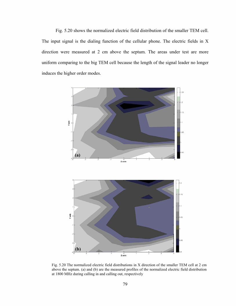
79
Fig. 5.20 shows the normalized electric field distribution of the smaller TEM cell.
The input signal is the dialing function of the cellular phone. The electric fields in X
direction were measured at 2 cm above the septum. The areas under test are more
uniform comparing to the big TEM cell because the length of the signal leader no longer
induces the higher order modes.
Fig. 5.20 The normalized electric field distributions in X direction of the smaller TEM cell at 2 cm above the septum. (a) and (b) are the measured profiles of the normalized electric field distribution at 1800 MHz during calling in and calling out, respectively
(a)
(b)

80
Fig. 5.20 (a) and (b) show the uniform electric field around area under test, which
is the center area. This area is about one-third area, which agrees with the theory. The
circular area above the center area in Fig. 5.20 (a) shows the field distribution because
there is a leak at the access door, and it is the gap area between the septum and the side
shields.
5.2.4 The Magnetic Field Measurement
The experimental setup to determine the magnetic field is shown in Fig. 4.18. The
magnetic fields in Y direction at 500 MHz were measured 2 cm above the septum. The
construct magnetic probe was used instead of the electric probe. Fig. 5.21 shows the yz
plane of the magnetic field of the small TEM cell.
Fig. 5.21 The yz plane of the magnetic field in Y direction at 500 MHz of the smaller TEM cell measured 2 cm above the septum.

81
Fig. 5.21 shows the uniform magnetic field around area under test, which is the
center area. This area is about one-third of the total area, which agrees with Fig. 5.9,
when the areas covered by the two peaks of the upper and lower right are neglected. The
excess areas covered by the two peaks are because of the mismatch of the characteristic
impedance around the areas. The error could be due to the TEM cell dimension error
around the areas. However, comparing it to the simulation result of Fig. 5.9, the result is
reasonable because the peaks of both results show at the sides of the planes, and the
uniform electric fields are at the center of the planes.

82
Chapter 6: Conclusions
An experiment method to project a cell phone radiation inside a TEM cell for
biological effects studies is presenting in this research work. Two TEM cell were
designed and modified through simulations and experiments to study the electromagnetic
radiation susceptibility and biological effects of commercial cellular phones. The second
TEM cell design achieved all the basic objectives of the research project, while the first
was designed to produce ball park figures. The TEM cell provides the shielded
environment for protecting the signal interference when the experimental setup is used
for biological effects studies. In addition, projecting the cell phone signal inside the
usable area of the TEM cell, uniform electromagnetic fields is generated in the region
where the DUT is expected to be placed.
A double-ended monopole antenna was also designed and used as a signal
antenna leader for inducing cellular phone signals into the TEM cell between the inner
and outer regions of the cell. The electric probe and magnetic probe used in the
experiment were also designed and built in the laboratory. The electric probe was used
for the electric field measurement. The magnetic probe was used for the magnetic field
measurement. The TEM cell’s impedance, electric field, and VSWR were measured to
characterize the experimental setup.
Measurements of the coupled voltage and the field distribution indicate that the
best setup for maximizing the fields in a large area is when the cell phone is located
outside the TEM cell. In such a configuration the cell phone should also be co-polarized
with the signal leader. Further study on improvement in field uniformity suggested a
shorter signal leader and smaller TEM cell needs to be designed and assembled. The use

83
of a shorter signal leader results in a loss of the field strength. A smaller TEM cell, on the
other hand, reduces the effects from higher order modes with a reduction of a usable area.
Thus a trade-off between the two choices must be made.
The results suggest that these TEM cell setups can be applied to radio frequency
exposure of the biological cells and organs for controlled experiments. The test area is
large enough for Petri dishes to be placed inside the cell where cell exposure and
confluence tests can be performed. Another advantage of the setup is that, unlike
cuvettes, the cells can be of a single or double layer and thus the shielding effects of cells
under electromagnetic radiation can be minimized.
For the future work, either an asymmetric TEM cell or a GTEM cell needs to be
designed which would be better choices. The asymmetric TEM cell provides increasing
the areas under test about one sixth of the asymmetric TEM cell’s height. For the GTEM
cell or gigahertz TEM cell, it is operating at the high frequencies with lager areas under
test comparing to the areas under test with the same operating frequency of the TEM cell.

84
APPENDIX A MATLAB CODE
(CONVERT S11 TO TDR PLOT)
load 'bt1.csv'; % load the file which has S11 s=bt1(:,2:3); % All the rows of 2nd and 3rd columns Freq=bt1(:,1); % All rows but first column fvec_sim = [50e6:1000e6/1001:1000e6-1000e6/1001]; % from 50 to 1000 MHz, 1001 points number_rows=size(s); number_rows=number_rows(1,1); % number of rows for i=1:1:number_rows % turning them into proper imaginary notation s_procd(i,1)=s(i,1)+j*s(i,2); end fdelta = fvec_sim(2)-fvec_sim(1); fsim = max(fvec_sim)+fdelta; tsim = 1/fsim; % tsim is step in time. time = [0:tsim:1/fdelta-tsim]; s11 = interp1(Freq,s_procd,fvec_sim,'linear','extrap'); s11_windowed = s11.*(1 + cos(pi*fvec_sim/fsim))/2; t11 = ifft(s11_windowed); impedance = 50*(1+t11)./(1-t11); % Zo is 50 tdr = impedance; figure; plot(time,abs(impedance)); grid on; xlabel('time (in sec)'); ylabel('Impedance (in Ohms)'); title('TDR plot');

85
BIBLIOGRAPHY
[1]. T. Virki, Global Cell Phone Penetration Reaches 50 Percent, Thomson Reuters, Nov. 29, 2007.
[2]. J.C. Lin, Specific Absorption Rates (SARs) Induced in Head Tissue by Microwave
Radiation from Cell Phones, IEEE Ant. Propagat. Mag., vol. 42, No. 5, pp. 138, Oct. 2000.
[3]. J.C. Lin, Cell Phone Testing and Fundamental Scientific Research, IEEE Ant.
Propagat. Mag., vol. 43, No 4, pp. 156, Aug. 2001. [4]. J.C. Lin, Can Cell Phones Promote Brain Tumors: The Interphone Study?, IEEE
Ant. Propagat. Mag., vol. 47, No. 2, pp. 137, Apr. 2005. [5]. J.C. Lin, Health Effects of Cell-Phone Research Outcomes and Source of Funding,
IEEE Ant. Propagat. Mag., vol. 49, No. 2, pp. 154, Apr. 2007. [6]. M.L. Crawford, Generation of Standard EM Fields Using TEM Transmission Cells,
IEEE Trans. Electromagn. Compat., vol. EMC-16, pp. 189, Nov. 1974. [7]. M.L. Crawford, J.L. Workman, and C.L. Thomas, Expanding the Bandwidth of
TEM Cells for EMC Measurements, IEEE Trans. Electromagn. Compat., vol. EMC-20, pp. 368, Nov. 1978.
[8]. E.F. Andrews, H.B. Lim, D. Xiao, S. Khamas, P.L. Starke, S.P. Ang, A. Barker, G.G. Cook, L.A. Coulton, and A. Scutt, Investigation of SAR Uniformity TEM Cell Exposed Culture Media, IEEE AMS., pp.71, 2004.
[9]. M.L. Crawford, Measurement of EM radiation from electronic equipment using
TEM transmission cells, NBS international report, pp. 73-306, 1973
[10]. P.F. Wilson, D.C. Chang, and M.T. MA, Input Impedance of a Probe Antenna in a TEM cell, IEEE Trans. Electromagn. Compat., vol. EMC-26, No. 4, pp. 154-161, Nov. 1984.
[11]. J.R. Juroshek, and C.A. Hoer, A High-Power Automatic Network Analyzer for Measuring the RF Power Absorbed by Biological Samples in a TEM cell, IEEE Trans. Microwave Theory Tech., vol. MTT-32, No. 8, pp. 818-823, Aug. 1984.
[12]. X.D. Cai, and G.I. Costache, Theoretical Modeling of Longitudinal Variations of
Electric Field and Line Impedance in TEM cells, IEEE Trans. Electromagn. Compat., vol. 35, No. 3, pp. 398-401, Aug. 1993.

86
[13]. R. Lorch, and G. Monich, Mode Suppression in TEM cells, IEEE Electromagn. Compat. Symp. Proc., pp. 40-42, Aug. 1996.
[14]. J.C. Rasmussen, B. Scholl, T. Gellekum, and H.J. Schmitt, Fiber-Optic
Temperature Sensor for Characterizing a 900 MHz TEM cell used in Bioeffects Dosimetry Studies, IEEE Eng. Med. Biol. Soc., vol. 5, pp. 1875-1876, Oct. 1996.
[15]. M. Popovic, S.C. Hagness, and A. Taflove, Finite-Difference Time-Domain
Analysis of a Complete Transverse Electromagnetic Cell Loaded with Liquid Biological Media in Culture Dishes, IEEE Trans. Biomed. Eng., vol. 45, No. 8, pp. 1067-1076, Aug. 1998.
[16]. R.D. Smedt, S. Criel, F. Bonjean, G. Spildooren, G. Monier, B. Demoulin, and J. Baudet, TEM Cell Measurements of an Active EMC Test Chip, IEEE Int. Symp. Biomed. Electromagn. Compat., vol. 2, pp. 903-908, Aug. 2000.
[17]. F. Fiori, and F. Musolino, Measurement of Integrated Circuit Conducted Emissions by Using a Transverse Electromagnetic Mode (TEM) Cell, IEEE Trans. Electromagn. Compat., vol. 43, No. 4, pp. 622-628, Nov. 2001.
[18]. E.F. Andrews, H.B. Lim, D. Xiao, P.L. Starke, S.P. Ang, A.T. Barker, G.G. Cook,
L.A. Coulton, and A. Scutt, Investigation of SAR Uniformity in TEM Cell Exposed Culture Media, IEEE Antennas. Mea., pp. 71-74, May. 2004.
[19]. J. Schuderer, D, Spat, T. Samaras, W. Oesch, and N. Kuster, In Vitro Exposure Systems for RF Exposures at 900 MHz, IEEE Trans. Microwave Theory Tech., vol. 52, No. 8, pp. 2067-2075, Aug. 2004.
[20]. R. Sarimov, L.O.G. Malmgren, E. Markova, B.R.R. Persson, and I.Y. Belyaev, Non-thermal GSM Microwaves Affect Chromatin Conformation in Human Lymphocytes Similar to Heat Shock, IEEE Plas. Sci., vol. 32, No. 4, pp. 1600-1607, Aug. 2004.
[21]. F.C.A.I. Cox, V.K. Sharma, A.M. Klibanov, B. Wu, J.A. Kong, and D.W. Engels, A Method to Investigate Non-Thermal Effects of Radio Frequency Radiation on Pharmaceuticals with Relevance to RFID Technology, Proc. IEEE. EMBS Int. Conf., pp. 4340-4343, Aug. 2006.
[22]. Z. Modebadze, B. Partcvania, and T. Surguladze, Experimental and Numerical Study of Electromagnetic Field Influence on Mollusk Neurons, DIPED Proc., pp. 78-83, Oct. 2006.
[23]. T. Dlugosz, and H. Trzaska, Mirror Reflections in EMF Dosimetry, Int. Symp. EMC, pp. 515-518, Oct. 2007.

87
[24]. David M. Pozar, Microwave Engineering, John Wiley & Sons, Inc., New Jersey, 2005.
[25]. Reinaldo Perez, Handbook of Electromagnetic Compatibility, Academic Press, Inc., San Diego, California, 1995.
[26]. Mark I. Montrose, and Edward M. Nakauchi, Testing for EMC Compliance, John
Wiley & Sons, Inc., New Jersey, 2004 [27]. CST MICROWAVE STUDIO Educational Version, 2008. CST Computer
Simulation Technology. [28]. Operating Manual, Spectrum Analysis… Field Strength Measurement (AN 150-10),
Agilent Technology, Sep. 1976.
[29]. A. Tharakan, Analysis of Magnetic Loop Probes for Near Magnetic Field, Thesis, University of Missouri-Rolla, 2003.
[30]. S. Roleson, Spectrum EMC Testing Using Field Probes as EMI Diagnostic Tools,
Conformity, Mar. 2007.