a yield model for integrated circuits and its application …najm/papers/tcad07-najm.pdf · a yield...
TRANSCRIPT

574 IEEE TRANSACTIONS ON COMPUTER-AIDED DESIGN OF INTEGRATED CIRCUITS AND SYSTEMS, VOL. 26, NO. 3, MARCH 2007
A Yield Model for Integrated Circuits and ItsApplication to Statistical Timing Analysis
Farid N. Najm, Fellow, IEEE, Noel Menezes, Member, IEEE, and Imad A. Ferzli, Student Member, IEEE
Abstract—A model for process-induced parameter variations isproposed, combining die-to-die, within-die systematic, and within-die random variations. This model is put to use toward findingsuitable timing margins and device file settings, to verify whethera circuit meets a desired timing yield. While this parametermodel is cognizant of within-die correlations, it does not requirespecific variation models, layout information, or prior knowl-edge of intrachip covariance trends. The approach works with a“generic” critical path, leading to what is referred to as a “process-specific” statistical-timing-analysis technique that depends only onthe process technology, transistor parameters, and circuit style. Akey feature is that the variation model can be easily built fromprocess data. The derived results are “full-chip,” applicable withease to circuits with millions of components. As such, this providesa way to do a statistical timing analysis without the need fordetailed statistical analysis of every path in the design.
Index Terms—Correlations, die-to-die variations, generic crit-ical path, parametric yield, principal component analysis, sta-tistical timing analysis, timing margin, virtual corner, within-dievariations.
I. INTRODUCTION
THE YIELD of integrated circuits can be thought of asthe ratio of the number of “functional chips” to that of
the total chips manufactured [1]. Traditionally, functionalityin the context of yield estimation and optimization has beentied to contaminations in the manufacturing process and silicondefects which lead to dramatic circuit faults (e.g., consider theconsequences of unwanted short circuits) [2]. This is referredto as functional yield or catastrophic-failure yield. Beyondcatastrophic failures, yield is also reduced when a number ofmanufactured chips does not meet target design specifications.The most important example for digital integrated circuits isthat some chips may fail to meet timing requirements in agiven process and are sorted into “low-speed bins” [3], resultingin yield loss for the high-speed design. This gives rise tothe concept of parametric yield, also known as circuit-limitedyield. With technology scaling, circuits are more exposed tothe adverse effects of process tolerances, and parametric yieldbecomes a crucial metric, especially in aggressive and high-speed designs. While the functional yield is primarily affected
Manuscript received November 26, 2004; revised June 7, 2005, October 3,2005, and March 8, 2006. This work was supported in part by the Intel Corpo-ration and in part by the Altera Corporation. This paper was recommended byAssociate Editor S. Sapatnekar.
F. N. Najm and I. A. Ferzli are with the Department of Electrical andComputer Engineering, University of Toronto, Toronto, ON M5S 3G4, Canada.
N. Menezes is with the Strategic CAD Labs, Intel Corporation, Hillsboro,OR 97124 USA.
Digital Object Identifier 10.1109/TCAD.2006.883924
by the process of manufacture and typically improves as theprocess matures [4], the parametric yield can be significantlyenhanced at the design stage through design awareness ofprocess variations and their impact on the overall circuit behav-ior. In this paper, we focus on the parametric part of the overallyield problem, with emphasis on timing margin budgeting,which directly relates to “timing yield” [5], [6].
As part of circuit-timing verification, one has to leave enoughmargin so that circuit-delay variations do not affect yield tooadversely. This has been usually taken care of by using a set ofworst case or corner-case files [7], [8] as part of timing veri-fication, typically during static timing analysis (STA). Corner-case files specify the values of transistor parameters for variousprocess corners, including the nominal and different extremesof device behavior. A standard practice for generating corners isto allow random variations of significant physical and electricalparameters across their ±3σ window (where σ is the standarddeviation of the variations) [3], and a circuit is deemed to havepassed the timing test if it meets the performance constraintsfor all these corners.
This conventional corner-case approach is becoming lessviable today, the main reason being the growing importanceof within-die variations [6] in state-of-the-art technologies. Forone thing, within-die variations appear as mismatches betweendevices or interconnect features on the same chip [5] and exhibitlocal layout-dependent trends. In consequence, an overwhelm-ing number of corner cases would be needed if one were toadequately capture these variations; and since layout informa-tion is available only late in the design, checking for within-dievariations becomes a final sign-off stage, impractical during theearly phases [9]. In addition, the corner-case approach providespass/fail outcomes, offering little or no quantitative feedback onthe robustness of the design [8].
Statistical techniques offer an alternative. Statistical tran-sistor modeling [8], [10] has been used for quite some time.Design centering [11], [12] methods have also been developedto tune the design to the manufacturing process. However, sta-tistical methods have generally suffered from being too slow tobe readily usable in a practical design methodology, aside fromthe inherent difficulty of gathering statistical data representativeof various levels of process variations and extracting from thisdata information that can be effectively useful for the designer.
While die-to-die variations take the same value for all in-stances of a given feature on a chip and can be easily mod-eled, within-die variations have a statistical dependence on thelocation within a chip and are intrinsically more problematic.They are of two types: systematic and random. Systematicvariations arise from the observed wafer-level variation trends
0278-0070/$25.00 © 2007 IEEE

NAJM et al.: YIELD MODEL FOR INTEGRATED CIRCUITS AND ITS APPLICATION TO TIMING ANALYSIS 575
reflected on a given die [9], [13] or the spatial locations of somefeatures on the die and their context in terms of the neighboringlayout patterns. They account for the spatial correlations dueto physical parameter variations across a chip. Random varia-tions constitute the residual component of the total variationswhich, in essence, cannot be explained systematically [13]and are modeled by statistically independent Gaussian randomvariables (RVs) [13], [14]. Ideally, one would like to extractsystematic variations and treat them as “deterministic” [15],[16]. This approach, however, necessitates detailed variationmodels and is hard to apply in the early design stages. A keycontribution of this paper is to deal with statistical within-dievariations, both systematic and random.
Recently, there has been a growing interest in tackling thetiming-yield problem by employing statistical techniques aspart of the circuit-timing analysis step. The aim is to extendtraditional STA so that it takes into account statistical de-lay variations [5], [6], [16]–[22] leading to a statistical STA(SSTA). Given the difficulty of early estimation of system-atic within-die variations, they have often been ignored; thus,within-die variations were accounted for on a random basisonly [6], [13], [18], [21], [22], which is undesirable. In orderto avoid making this assumption, one needs to express thewithin-die correlations with a model that can be easily builtfrom process data. This point is key, and is hard to do—thereare no published models, for instance, for how exactly thevariations are correlated across the die as a function, say, of thedistance between components. A model of correlations in termsof distance is mentioned and used in [23], but no details or dataare given; it is not clear what shape the model should take foran arbitrary parameter nor how one would build it from processdata. In [16], even though statistical within-die variations arenot taken into account, a suggestion is made as to how onemay include them and take care of correlation by enforcingcorrelation between neighboring features on a die. This themewas further developed recently where use was made of principalcomponent analysis (PCA) [20] or a quad-tree partitioning [19]to express a regionwise spatial within-die correlation. Here, too,it is not clear how one would identify these regions and how themodel would be built from process data. Finally, these methodsdepend on placement information, making them hard to useduring circuit design and optimization.
The basic question that serves as premise to this paper is:Prior to design, what can be said regarding circuit charac-teristics? From the process/technology end, we assume thatone is able to know device/interconnect-delay sensitivities andthe extent of die-to-die and within-die correlations, withoutknowing how these correlations will affect different elementsof the design once placement is done. Our analysis will accountfor this knowledge and will thus introduce a level of awarenessof process variations, including their correlation, at this earlystage of the design cycle. From the design side, we assumethat one is able to make certain design decisions pertaining to“design style,” such as the typical number of critical paths ortheir depth in a circuit. Then, given a target process technology,transistor models, and circuit design styles, the methodologypresented in this paper can be applied to suggest preferreddesign styles (e.g., in terms of the number of high-speed
paths and their depths) or find preferred device characteristics(e.g., in terms of device delay sensitivities) which would fore-cast higher timing yields once the design is completed, consid-ering that process variations are correlated but their correlationsstill unknown at the time of the analysis. The quantitative mea-sure will come in the form of yield bounds and yield-margincurves that hold regardless of how the correlation structure ofthe process-induced variations in each physical parameter willlook like once the placement is complete. Yield-margin curvescan be used to quantify yield loss at a given timing margin. Ouranalysis will also result in a selection of “device file” settingslying within the extremes of device behavior with which to rundeterministic STA, so that a given timing-yield requirement canbe met. Our work, of which a preliminary version appeared in[24], straddles traditional STA and design space explorationtechniques under process variations and links circuit-timinganalysis as done today through the STA with process-inducedparametric yield.
For example, while the “nominal” device file may call fora setting of ∆L = 0 (for channel-length variations) and the“worst case” file may call for a setting of ∆L = +3σL, ourapproach can be used to predict the value “δ,” which we referto as a virtual corner, such that if the setting of ∆L = δσL isused for all devices, and if the circuit timing is verified usingdeterministic STA, then the circuit will achieve the desiredtiming yield. Therefore, our approach preserves existing statictiming methodology and only assumes the existence of statisti-cal transistor models, which have been standard for some time.
We will perform our analysis using the concept of “genericcritical path,” in the style of [23], by examining the statisticalproperties of large ensembles of such paths. The validity of thegeneric-path model in the context of circuit-timing analysis wasverified by a separate set of experiments described in the appen-dix of this paper. The generic paths will enable us to abstractmost circuit-specific information and obtain estimates of yieldloss considering a model of process variations including die-to-die and within-die with correlations. The model of genericpaths is pertinent to circuit-timing analysis insofar as differentcircuits share fundamental characteristics which impact timingyield, and we think it is intuitively reasonable to use the generic-path model to capture the way logic paths contribute to timing-yield loss. It is well known, for instance, that the timing yieldof highly optimized circuits is determined by a relatively largenumber of paths of comparable delay. This phenomenon ofthe “wall of paths” clustered close to the clock edge as aresult of circuit optimization has been widely reported in theliterature [25] and forms an intuitive basis for the generic-pathmodel. Under this model, our analysis can serve as a theoreticalframework for understanding the timing-yield implications ofprocess variability.
The rest of this paper is organized as follows. Section IIintroduces our generic parameter model, combining die-to-dieand systematic and random within-die (WDR) variations. InSection III, we build a model for circuit timing starting from thephysical device and interconnect variations and show how cir-cuit timing fits with our generic parameter model. Then, after abrief summary in Section IV, we gradually look at the impact ofindividual variation components on parametric yield. Section V

576 IEEE TRANSACTIONS ON COMPUTER-AIDED DESIGN OF INTEGRATED CIRCUITS AND SYSTEMS, VOL. 26, NO. 3, MARCH 2007
examines the situation where parameter variation is consideredentirely die to die. Section VI adds within-die variations aspurely random, and the full variation model is addressed inSection VII, with an application to circuit timing illustratedin Section VIII. When systematic within-die variations areexcluded, our approach is to compute simple expressions to es-timate parametric yield. When these variations are included, wederive readily usable expressions to bound the yield from aboveand below. Throughout this paper, we will derive the resultsfirst on a generic parameter, then illustrate them with a directapplication to circuit timing. We will compare the necessarytiming margins and case file settings in different situations byfollowing a simple case where variation is progressively splitbetween different components, and a specified timing yield isrequired. We conclude in Section IX.
II. PARAMETER MODEL
For a given circuit element or layout feature i, let its co-ordinates on the die be (xi, yi) and let X(i) be a GaussianRV that denotes the variation of a certain parameter of thiselement from its nominal (mean) value. Thus, for example,X(i) may represent channel-length variations of transistor i.Let n be the number of occurrences of this parameter on achip. For simplicity, we consider X(i) to be zero mean, withthe understanding that a mean shift can be easily incorporatedinto the model below.
We break down X(i) into a die-to-die component Xdd and awithin-die component Xwd, such that
X(i) = Xdd +Xwd(i), i = 1, . . . , n. (1)
Here, Xdd is a zero-mean Gaussian RV that takes the samevalue for all instances of an element on a given chip, irrespec-tive of location, while Xwd(i) is a zero-mean Gaussian RVwhich can take different values for different instances of anelement on the same die. We consider Xdd to be independentof Xwd(i), ∀i. This leads to the following relationship betweenthe variances:
σ2(i) = σ2dd + σ2
wd(i) (2)
where σ2(i), σ2dd, and σ2
wd(i) are the respective variances ofX(i), Xdd, and Xwd(i).
Within-die variation is further broken down into system-atic and random components, respectively, as Xwds(i) =Xwds(xi, yi) and Xwdr(i)
Xwd(i) = Xwds(xi, yi) +Xwdr(i), i = 1, . . . , n (3)
where each of these components is itself a zero-mean GaussianRV. Systematic variations capture all location-dependentwithin-die correlations, so that Xwds(xi, yi) and Xwdr(j) areindependent, ∀i, j, and Xwdr(i) and Xwdr(j) are independent,∀i �= j. The following relationship can then be written forwithin-die variance:
σ2wd(i) = σ2
wds(xi, yi) + σ2wdr(i) (4)
where σ2wd(i), σ2
wds(xi, yi), and σ2wdr(i) are the variances of
Xwd(i), Xwds(xi, yi), and Xwdr(i), respectively.
The problem clearly lies in knowing and managing the jointdistribution of the systematic variations. The covariance matrixitself, which may contain an information pertaining to millionsof instances of a parameter on a given chip, is hard to estimate;and even when it is available, numerical operations can becomeextremely difficult. One way to express the systematic varia-tions is to use the PCA [26] and write
Xwds(i) =p∑
j=1
aijZj (5)
where Zj are independent standard normal RVs (Gaussianswith zero mean and unity variance), and p � n is the order ofthe expansion. The RVs Zj correspond to underlying indepen-dent unobservable factors. The value of p and the coefficientsaij represent the extent of correlation across the die. For exam-ple, if p = 1, then the within-die spatial correlation coefficientis one: There is a perfect correlation; a single underlyingRV Z1 determines the value of the systematic component ofXwd all over the die. A p > 1 allows for less than perfectcorrelation.
We will adopt the PCA expansion (5) as our “correlationmodel” for the within-die component. At first glance, thismodel appears hard to use because it seems to depend on knowl-edge of the values of all the aij parameters. These coefficientsdepend on the correlation structure of physical parameters onthe chip. In other words, a full PCA cannot be used to assess theimpact of statistical variations on the design until after layoutwhen the spatial locations of devices on chip are known. Eventhen, it is not clear how one would compute them from processdata. A brute-force PCA over the millions of instances of aparameter on a chip would be impractical. However, withoutany explicit knowledge of the correlations, we will capitalizeon the following property that relates the PCA coefficients tothe parameter variances:
σ2wds(xi, yi) =
p∑j=1
a2ij . (6)
Using this property, and without knowing the specifics ofsystematic variations, including die-level trends and layout in-formation, we will obtain lower/upper bounds on the parametricyield that require only: 1) the order p of the PCA expansion, and2) representative values (maximum, minimum, average) of thevariance terms given previously.
III. TIMING MODEL
This section shows how a model for circuit timing can bebuilt to conform with the generic model discussed in Section IIand whose characteristics are obtainable from process files.Working toward the delay of a multistage generic critical path,we start with the physical variations of transistor thresholdvoltage and channel length. Physical variations lead to stage-delay variations, where a stage consists of a gate with fan-out interconnect, and we discuss interconnect-level variations.Finally, stage-delay variations are used to characterize path-delay variations as a generic parameter.

NAJM et al.: YIELD MODEL FOR INTEGRATED CIRCUITS AND ITS APPLICATION TO TIMING ANALYSIS 577
A. Device Variations
In deep submicrometer CMOS, process-induced delay vari-ations are mainly due to variations in the MOSFET thresholdvoltage (Vt) and effective channel length (Le). Due to short-channel effects, Vt may decrease with decreasing Le (the Vt
roll-off [3] effect), so that Vt and Le are not independentvariables. We assume that for small Le variations, denoted byL, threshold voltage roll-off is linear with channel-length varia-tion, and we express Vt as the sum of a linear term that dependson Le (K∆Le, where K > 0) and another term representingvariations of Vt which are independent of Le, denoted by V .With E[·] being the expected (or mean) value operator, we canexpress Vt and Le of transistor i as follows:
Le(i) = E [Le(i)] + L(i) (7)
and
Vt(i) = E [Vt(i)] +KL(i) + V (i). (8)
We are interested in the RVs L(i) and V (i), which are assumedto be zero-mean Gaussian and independent of each other. Wecan thus break them up in the usual manner as
L(i) =Ldd + Lwds(xi, yi) + Lwdr(i)
V (i) =Vdd + Vwds(xi, yi) + Vwdr(i). (9)
(Of course, here, Vdd is the die-to-die component of V (i), andnot the supply voltage.) The variances of L(i) and V (i), as wellas the variance of their components, can be known from thetechnology files
σ2L(i) =σ2
dd,L + σ2wds,L(xi, yi) + σ2
wdr,L(i) (10)
σ2V (i) =σ2
dd,V + σ2wds,V (xi, yi) + σ2
wdr,V (i). (11)
B. Gate Delay
We assume that, for a given chip design in a given tech-nology, one can define a “nominal” representative logic gate,with appropriate output loading and input slope. For reasonsthat will become clear, this gate should be typical of gates oncritical paths in this technology. Due to the nonlinearity of therelationship between gate delay and transistor parameters, themean value of gate delay does not necessarily coincide withits nominal value [the value corresponding to the case whenL(i) = 0 and V (i) = 0]. Furthermore, the distribution of gatedelay would not necessarily be Gaussian. Simple experimentswith HSPICE, however, reveal that this nonlinearity is notstrong, at least not in 0.13-µm CMOS. Therefore, we willignore these complications and simply assume that gate delayis linearly dependent on transistor parameter variations, so thatit becomes a Gaussian variable with mean equal to its nominalvalue. Another consequence of this linearity assumption is that,ifD(i) is the deviation of the delay of logic gate i from its mean(nominal) delay, then
D(i) = α0L(i) + β (V (i) +KL(i)) (12)
where α0 and β are sensitivity parameters, with suitable units,that one can easily obtain from circuit simulation of a repre-sentative logic gate. Notice that, in general, α0 > 0 and β > 0.(For a specific industrial 0.13-µm process, we have foundthat for a minimum-sized inverter, α0 ≈ 0.857 ps/nm and β ≈17.3 ps/V.) Let s1 = α0 +Kβ and let s2 = β. Then, we have
D(i) = s1L(i) + s2V (i). (13)
Now, we define the following:
Ddd = s1Ldd + s2Vdd
Dwds(xi, yi) = s1Lwds(xi, yi) + s2Vwds(xi, yi)
Dwdr(i) = s1Lwdr(i) + s2Vwdr(i). (14)
Clearly, Ddd, Dwds(xi, yi), and Dwdr(i) represent die-to-die,WDS, and WDR variations of gate delay, corresponding to theparametric model discussed in Section II. As a result, we candefine the three components of the total gate-delay varianceσ2
dd,D, σ2wds,D(xi, yi), and σ2
wdr,D(i) and compute them fromthe variations of channel length and threshold voltage using(10), (11), and (14).
C. Interconnect Delay
Gate delay is one factor in total path delay, the other be-ing interconnect. We extend the previous analysis to includeinterconnect-delay variations by considering each stage on apath to comprise a gate with corresponding fan-out intercon-nect. Let τ(i) be the delay of the interconnect line in stage i.Similar to a generic gate, we assume that each stage can becharacterized by a nominal interconnect delay τ0(i) that is thesame for all stages, i.e., τ0(i) = τ0, ∀i. In a simple model,τ(i) = R(i)C(i), where R(i) and C(i) are, respectively, theresistance and capacitance of line i [27]. If ρ is the metalresistivity and εox is the oxide permittivity, then
R(i) =ρl(i)
w(i)t(i)C(i) =
εoxw(i)l(i)TILD(i)
where l(i) and w(i) are, respectively, the metal length andwidth, and t(i) and TILD(i) are, respectively, the thicknessesof the interconnect and the interlayer dielectric (ILD) oxide, instage i. Then, we have
τ(i) =ρεoxl(i)2
t(i)TILD(i). (15)
Denote by t0 and TILD,0 the nominal values of metal and ILDthicknesses and let t(i) = t0 + ∆t(i) and TILD(i) = TILD,0 +∆TILD(i). Neglecting the second-order term ∆t(i)∆TILD(i),we write
τ(i) ≈ ρεoxl(i)2
t0TILD,0 + TILD,0∆t(i) + t0∆TILD(i)
=τ0
1 + ∆t(i)t0
+ ∆TILD(i)TILD,0
. (16)
578 IEEE TRANSACTIONS ON COMPUTER-AIDED DESIGN OF INTEGRATED CIRCUITS AND SYSTEMS, VOL. 26, NO. 3, MARCH 2007
Let ∆τ(i) = τ(i) − τ0, then
∆τ(i)τ0
=−(
∆t(i)t0
+ ∆TILD(i)TILD,0
)1 +(
∆t(i)t0
+ ∆TILD(i)TILD,0
) . (17)
Let u = ∆t(i)/t0 + ∆TILD(i)/TILD,0. Assuming small (rela-tive) variations in ILD and metal thicknesses, |u| � 1, whichleads to
∆τ(i) ≈ − τ0t0
∆t(i) − τ0TILD,0
∆TILD(i)
= − s3∆t(i) − s4∆TILD(i). (18)
Supposing zero-mean Gaussian deviations in ILD and metalthickness, we consider each to be a generic parameteras in Section II, with corresponding variation components(TILD,dd, TILD,wds, TILD,wdr) and (tdd, twds, twdr) and theirrespective variance triplets (σ2
TILD,dd, σ2TILD,wds, σ
2TILD,wdr) and
(σ2t,dd, σ
2t,wds, σ
2t,wdr).
While advanced interconnect variation models have beendeveloped [28]–[30] and may depend on several physical para-meters, we assume that in any case, it is possible to express theinterconnect-delay variation as a linear summation of physicalparameters Pi, in the form
∆τ(i) ≈∑
±siPi.
For simplicity, the analysis to follow includes only variations inILD and metal thicknesses, as given in (18).
D. Stage Delay
Considering each stage to represent a gate with correspond-ing fan-out interconnect, we can now express stage-delay devi-ation S(i) as follows:
S(i)=D(i)+∆τ(i)
= [s1Ldd+s2Vdd−s3tdd−s4TILD,dd]
+[s1Lwds(xj , yj)+s2Vwds(xj , yj)
− s3twds(xj , yj)−s4TILD,wds(xj , yj)]
+[s1Lwdr(i)+s2Vwdr(i)−s3twdr(i)−s4TILD,wdr(i)] .
(19)
The die-to-die, WDS, and WDR components of the variationsin stage delay are readily identifiable from (19). Stage delaytherefore conforms with the model for a generic parameter inSection II, in the sense that it has three variance componentswhich can be computed from physical parameter variances,with the die-to-die component being the same for all stages andthe within-die random components of two distinct stages beingstatistically independent.
E. Path Delay
Consider a path with a number N of logic stages, represen-tative of a circuit’s typical critical paths, which we will refer toas a generic critical path. Assume that path j comprises stages1, . . . , N and let DN (j) denote the deviation of the delay ofpath j from its mean (nominal) value. Then
DN (j) =N∑
i=1
S(i)
=NSdd +N∑
i=1
Swds(xi, yi) +N∑
i=1
Swdr(i) (20)
where Sdd, Swds(xi, yi), and Swdr(i) are the die-to-die, WDS,and WDR variations in stage delay, derived in (19).
The gates on a path exist at various different locations. Wemake the simplifying assumption that as far as physical locationon the die, for purposes of computing the within-die-systematiccomponent, all gates (and stages) on path j share the same“nominal” coordinates (xj , yj), so that
DN (j) = NSdd +NSwds(xj , yj) +N∑
i=1
Swdr(i). (21)
This approximation is motivated by the expectation that gateson a critical path should be nearby on the die, and differencesbetween their position-dependent within-die-systematic varia-tions should be minor. We note that this may no longer be truein latch-based designs that make use of a cycle stealing, andwhere critical paths may span large distances.
Using (19), we arrive at the following relationship betweenpath-delay and physical parameter variations:
DN (j) = [Ns1Ldd +Ns2Vdd −Ns3tdd −Ns4TILD,dd]
+ [Ns1Lwds(xj , yj) +Ns2Vwds
− Ns3twds(xj , yj) −Ns4TILD,wds(xj , yj)]
+
[s1
N∑i=1
Lwdr(i) + s2
N∑i=1
Vwdr(i)
− s3
N∑i=1
twdr(i) − s4
N∑i=1
TILD,wdr(i)
]. (22)
We can readily identify the die-to-die, WDS, and WDR compo-nents of path delay from the previous expression. It can be seenthat the systematic component is the same for all the consideredgeneric critical paths. Assume that the considered paths j =1, 2, . . . are disjoint, then the random components of path delaybecome strictly independent from one another and the structureof the generic parameter introduced in Section II is preserved.In the sequel, we will consider that path delay conforms withour generic parameter model, with three variance componentsrelated to physical parameters and obtained from process data,and such that its die-to-die component is the same for allinstances (on the same die), its WDR components are inde-pendent for different instances, and its WDS components are

NAJM et al.: YIELD MODEL FOR INTEGRATED CIRCUITS AND ITS APPLICATION TO TIMING ANALYSIS 579
spatially correlated due to WDS physical parameter variations.For practical purposes, the assumption of disjoint paths is notrestrictive and is needed to ensure that random componentsof path delay remain strictly uncorrelated. Recall that we arelooking at generic paths which are representative of all thechip’s critical paths, and the number of such disjoint paths iseffectively large enough so that any statistics inferred on such adisjoint group reflect those of the critical paths collectively.
Based on the independence relations between the terms in(22), we now have expressions for the variance triplet of pathdelay, so that we can write
σ2DN
(j) = σ2dd,DN
+ σ2wds,DN
(xj , yj) + σ2wdr,DN
(j) (23)
where
σ2dd,DN
=N2s21σ2dd,L +N2s22σ
2dd,V +N2s23σ
2dd,t +N2s24σ
2dd,TILD
(24)
σ2wds,DN
(xj , yj)
=N2s21σ2wds,L(xj , yj) +N2s22σ
2wds,V (xj , yj)
+N2s23σ2wds,t(xj , yj) +N2s24σ
2wds,TILD
(xj , yj) (25)
σ2wdr,DN
(j)
=Ns21σ̂2wdr,L(j) +Ns22σ̂
2wdr,V (j)
+Ns23σ̂2wdr,t(j) +Ns24σ̂
2wdr,TILD
(j) (26)
where σ̂2wdr,L(j), σ̂2
wdr,V (j), σ̂2wdr,t(j), and σ̂2
wdr,TILD(j) are
the average variances of the within-die random variations ofthe corresponding physical parameters taken over path j. Thesepath averages may be approximated by averages over the wholedie, so that we write
σ̂2wdr,V (j) ≈ σ̂2
wdr,V
σ̂2wdr,L(j) ≈ σ̂2
wdr,L
σ̂2wdr,t(j) ≈ σ̂2
wdr,D
σ̂2wdr,TILD
(j) ≈ σ̂2wdr,TILD
.
In turn, we can approximate the variance of delay on path j dueto WDR parametric variations as a die-level average variance,in other words
σ2wdr,DN
(j) ≈ σ̂2wdr,DN
. (27)
As usual, we define σ̂2wdr,DN
to be the average value ofσ2
wdr,DN(j) across the die. An important observation from
(24)–(26) is that, unlike the two other components, WDR vari-ance grows with N , not N2. This gives a preliminary insight onthe effect of random variations on path delay “averaging out,”or becoming significantly less manifest than other variationcomponents over paths with a large number of stages. We willreturn to this point in the subsequent analysis.
IV. PARAMETRIC AND TIMING YIELD
A key component of our approach is the application of thegeneric parameter yield model developed previously to pathdelay, and using that to compute chip timing yield. The reasonwe can do this is because, as shown, we can express the varianceof path delay, for a large collection of critical generic paths, as astandard variance model with die-to-die, within-die systematic(WDS), and within-die random (WDR) components. With this,we can effectively talk about delay (be it of a gate, a stage, or apath) as being a “parameter.”
Throughout this paper, we define the yield of a certainparameter X as the probability of satisfying a constraint onthe maximum value of the parameter on a chip (with theunderstanding that the results to follow can be extended to coverminimum values and interval constraints)
Y (x) = P {X(i) ≤ x, i = 1, 2, . . . , n} (28)
where n is the number of instances of that parameter on thedie. We write Y (x) to refer to the yield of a generic parameterand denote specifically by Y(d) a timing yield. In the followingsections, we will build our way gradually to a full model of chiptiming yield by first investigating the timing yield when onlydie-to-die variations are considered, then when only die-to-dieand WDR variations are considered, before finally presentingthe full model. This improves the clarity of the results, and alsoallows us to highlight interesting results that arise when onlycertain variation components are dominant.
V. DIE-TO-DIE YIELD
We start by considering only die-to-die variations.
A. Generic Parameter
We define the die-to-die yield of a generic parameter X as
Ydd(x) = P{Xdd ≤ x} = Φ(
x
σdd
)(29)
where P{·} is a probability, Φ(·) is the cumulative distributionfunction (cdf) of a standard normal RV, and σdd is the varianceof the die-to-die component of X . Since Xdd(i) = Xdd, ∀i, thedie-to-die yield is governed by a single RV.
B. Timing Yield
The simple expression in (29) can be directly used to estimatethe die-to-die timing yield Ydd(d), replacing σdd by σdd,DN
,obtained from (24). Fig. 1 plots the values of die-to-die timingyield versus the timing margin d, where d is normalized innumbers of standard deviations σ = σdd,DN
.Now, suppose that a value Y is desired for the die-to-die
timing yield. Then, we have
d =Y−1dd (Y)
=Φ−1(Y)σdd,DN. (30)
We can interpret (30) in two ways. Suppose that d0 is thecritical path delay when the nominal process files are used,
580 IEEE TRANSACTIONS ON COMPUTER-AIDED DESIGN OF INTEGRATED CIRCUITS AND SYSTEMS, VOL. 26, NO. 3, MARCH 2007
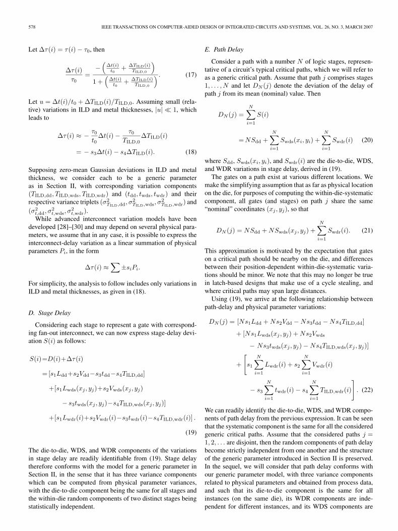
Fig. 1. Timing yield when considering die-to-die variations alone.
i.e., excluding process variations. If the nominal timing mar-gin (e.g., Tclk − d0, where Tclk is the clock period) exceedsY−1
dd (Y), then the timing yield Y is met.Alternatively, if a corner-case process file is set to produce
a delay of d0 + Y−1dd (Y) while still meeting the timing con-
straints, then the die-to-die yield Y is achieved. Therefore,we refer to plots such as Fig. 1 as yield-margin curves. Forexample, such a corner file can be built simply by allowing adelay deviation of Y−1
dd (Y)/N at each of the N stages of thecritical path. In turn, stage physical parameters can be modifiedso that stage delay deviates by this amount. S(i) being the delayof stage i, we let
Y−1dd (Y)N
=S(i), i = 1, . . . , n
= s1L(i) + s2V (i) − s3∆t(i) − s4∆TILD(i)
= Φ−1(Y)σdd,DN
N(31)
where the last equality follows from (30). This gives a rangeof possible settings of the physical parameters that achieve atiming deviation of Y−1
dd (Y) over N -stage paths. For simplicityof illustration, if we impose on our corner-case files equalrelative deflection (i.e., deviation from the mean or nominalvalue) of the physical parameters, i.e.
L(i)σdd,L
=V (i)σdd,V
= −∆t(i)σdd,t
= −∆TILD(i)σdd,TILD
= δ, ∀i (32)
then
δ =Y−1
dd (Y)/Ns1σdd,L + s2σdd,V + s3σdd,t + s4σdd,TILD
(33)
is the value of the process file setting which, when applied to allthe parameters, causes the right amount of path-delay deflectionY−1
dd (Y) to be created so as to “test” the circuit for timingyield Y .
It is of interest to note the following. Recall from (24) thatthe die-to-die path-delay variance is as follows:
σ2dd,DN
= N2(s21σ
2dd,L + s22σ
2dd,V + s23σ
2dd,t + s24σ
2dd,TILD
).
(34)
Since the square of the sum of positive quantities is larger thanthe sum of their squares, then
σdd,DN≤ N(s1σdd,L + s2σdd,V + s3σdd,t + s4σdd,TILD).
(35)
From (30) and (33), it then follows that
δ ≤ Φ−1(Y). (36)
Thus, when equal deflections of the physical parameters areassumed, then δ, for a desired die-to-die yield Y , is at mostΦ−1(Y), irrespective of the specific variance values.
In order to get a sense of typical values for δ, assume forsimplicity that path-delay variance is equally divided amongchannel length, threshold voltage, dielectric thickness, and wirethickness, that is
s21σ2dd,L = s22σ
2dd,V = s23σ
2dd,t = s24σ
2dd,TILD
= s2
and suppose a die-to-die yield of 95% is desired. From Fig. 1,we get that Y−1
dd (95%) = 1.6σdd,DN. Then, each stage delay
may be set to Y−1dd (95%)/N = 1.6σdd,DN
/N = 3.2s. Impos-ing equal relative deflection in interconnect and device parame-ters, therefore using (33), yields
δ =3.2s4s
= 0.8. (37)
To sum up, δ defines a “corner-case” file for which thecircuit should be tested for timing-constraint violations. If thecircuit satisfies the timing constraints with this δ setting, then itwould have a die-to-die timing yield of Y . Observe that this filesetting is not unique in the sense that any corner-case file whichproduces a delay deviation of Y−1
dd (Y) around the nominal delayeffectively serves the same purpose. Our particular derivationof the case file simply imposed equal stage timings and similarrelative deviation in transistor physical parameters. We refer tothese corners (defined by a δ value) that lie between deviceextremes and that could be used to design for a certain targetyield as virtual corners.
VI. YIELD CONSIDERING DIE-TO-DIE
AND WDR VARIATIONS
In this section, we consider only the die-to-die and WDRvariations.
A. Generic Parameter
We start by considering a generic parameter X . LetYdd,wdr(x) be the yield of X considering die-to-die and WDRvariations of X . If n is the number of instances of X on thechip, then
Ydd,wdr(x) =P{Xdd +Xwdr(i) ≤ x, i = 1, . . . , n}=P{Xwdr(i) ≤ x−Xdd, i = 1, . . . , n}. (38)
We now recall a result from a basic probability theory thatwill be used repeatedly in this paper. Let A be an arbitrary event

NAJM et al.: YIELD MODEL FOR INTEGRATED CIRCUITS AND ITS APPLICATION TO TIMING ANALYSIS 581
andX be an RV with a probability density function (pdf) fX(·).Then, we have (see [31, p. 85])
P{A} =
+∞∫−∞
P{A|X = x}fX(x)dx. (39)
This result is simply an extension to the continuous case of thesimple fact that P{A} = P{A|B} · P{B} + P{A|B} · P{B},where B is another event. Applying (39) to (38) and denotingby fXdd(·) the pdf of Xdd, give
Ydd,wdr(x)
=
+∞∫−∞
P {Xwdr(i) ≤ x−Xdd, ∀i|Xdd = z} fXdd(z)dz
=
+∞∫−∞
P {Xwdr(i) ≤ x− z, ∀i|Xdd = z} fXdd(z)dz
=
+∞∫−∞
P{Xwdr(i) ≤ x− z, ∀i}fXdd(z)dz (40)
where the transition between the second and third equation in(40) is due to the statistical independence of Xdd and Xwdr(i),∀i. If φ(·) denotes the pdf of the standard normal distribution,then fXdd(z) = φ(z/σdd)/σdd. Letting z0 = z/σdd and usingthe statistical independence of Xwdr(i) and Xwdr(j) for i �= j,we can write (40) as
Ydd,wdr(x) =
+∞∫−∞
n∏i=1
Φ(x− z0σdd
σwdr(i)
)φ(z0)dz0. (41)
We now introduce another basic result from the probabilitytheory that will be used repeatedly in this paper, which iscommonly referred to as the law of the unconscious statistician.If X is an RV with pdf fX(·) and if g(·) is a function, then, (see[31, p. 106]) the mean of g(X) can be written as
E [g(X)] =
+∞∫−∞
g(x)fX(x)dx. (42)
Based on this, and if we define Z0 to be an independent1
standard normal RV, then (41) can be written as
Ydd,wdr(x) = E
[n∏
i=1
Φ(x− Z0σdd
σwdr(i)
)]. (43)
We have so far assumed the parameter variations to beGaussian, which technically allows the variations to extend to±∞, allowing for nonphysical situations. In reality, one wouldexpect the process variations to be bounded by some upper and
1Throughout this paper, whenever an individual RV is described as “indepen-dent,” this means that it is independent of all other RVs under consideration.
lower bounds, as process tolerances fall within a certain range.If a device somewhere deviates by larger amounts, then chancesare, there is a serious problem with that die, and that it wouldbe lost due to other reasons, that is, other than timing yield.Therefore, when estimating a parametric yield, we truncate nor-mal variations at ±kσ, where k is an arbitrary positive numberand σ is the standard deviation of the untruncated distribution.For simplicity of presentation, we apply the truncation onlyto the within-die random variations, since this is where thenonphysical tails of the normal distribution have a big effecton the yield estimates because the cdfs of the WDR variationsare multiplied n times, as can be observed in (43).
We affect the truncation of the normal distribution by condi-tioning it over the interval [−kσ,+kσ], leading to the so-calledtruncated normal distribution. Let Φk(·) denote the cdf of thestandard normal distribution truncated at ±k, so that
Φk(x) =
0, x < −kΦ(x)−Φ(−k)Φ(k)−Φ(−k) , −k ≤ x ≤ k
1, x > k.
It can be easily verified that if X is a zero-mean Gaussian RV,with standard deviation σ and cdf Φ(x/σ), then conditioningX on being in the interval [−kσ,+kσ] yields the cdf Φk(x/σ).We now write (43) as follows:
Ydd,wdr(x) = E
[n∏
i=1
Φk
(x− Z0σdd
σwdr(i)
)]. (44)
This can be easily computed by numerical integration usingthe integral form (41), with Φk(·) used in place of Φ(·).Fig. 2 shows the resulting yield-margin curves, where we haveassumed for simplicity that σwdr(i) is constant across the die:σwdr(i) = σwdr, we have assumed that σ2
dd = σ2wdr, and we
define σ2 = σ2dd + σ2
wdr, so that σdd = σwdr = σ/√
2. Thevalues on the x axis are normalized in multiples of this σ.The figure includes yield plots for three different values of n,each for both cases of untruncated random variations andrandom variations truncated at ±3σwdr. Effectively, truncatingthe distribution amounts to cutting off its “tail,” leading toless pessimistic yield estimates, especially for large n: then = 1e+ 06 and n = 1e+ 08 plots are indistinguishable.Comparing Fig. 1 with Fig. 2, we can readily contrast the levelof yield loss when all the variance is taken to be die to die withthat when the variance is split (equally, in our case) betweendie-to-die and WDR variations. For example, if the variationis attributed only to die-to-die effects, then we need to budget1.6σ to meet a yield of 95%. Considering the WDR variationsto be on a par with the die-to-die variations, the same yield levelis reached only at 3.2σ (for very large n and taking truncatedWDR variations), that is, the required margin doubles.
B. Timing Yield
Since we considered the path delay to conform to ourgeneric parameter model (see Section III-E), then the results ofSection IV-A can now be put to use in order to estimate the

582 IEEE TRANSACTIONS ON COMPUTER-AIDED DESIGN OF INTEGRATED CIRCUITS AND SYSTEMS, VOL. 26, NO. 3, MARCH 2007
Fig. 2. Comparison of parametric yield when using untruncated and truncateddistributions.
timing yield Ydd,wdr(d). Applying (44) to derive an expressionfor timing yield, and using (27), we get
Ydd,wdr(d) = E
[Φn
k
(d− Z0σdd,DN
σ̂wdr,DN
)]. (45)
For simplicity, we assume that the variance of each physi-cal parameter is equally split between die-to-die and WDRcomponents
σ2dd,L = σ̂2
wdr,L = σ2L/2
σ2dd,V = σ̂2
wdr,V = σ2V /2
σ2dd,t = σ̂2
wdr,t = σ2t /2
σ2dd,TILD
= σ̂2wdr,TILD
= σ2TILD
/2.
These and similar simplifying assumptions, made throughoutthis paper, are for illustration purposes only and do not affectthe generality of the approach. From (24) and (26), it followsthat σ2
dd,DN= Nσ2
wdr,DN(j). Then, using (23) and (27), we
can write
σ2dd,DN
= Nσ̂2wdr,DN
=N
N + 1σ2
DN(46)
where we have dropped the index j from σ2DN
(j) for simplicity,and because we have used the die average σ̂2
wdr,DNin the
equation. Plugging (46) into (45), we get
Ydd,wdr(d) = E
[Φn
k
(√N + 1
d
σDN
−√NZ0
)]. (47)
Fig. 3 plots Ydd,wdr(d) (with k = 3) for different values ofN and n. The yield-margin curves clearly show the impactof random variations on total path delay diminishing with thenumber of path stages.
We may follow the same approach as in Section V to com-pute the timing margins and derive corner-case files in orderto check the circuit-timing yield. Once again, a timing marginof Y−1
dd,wdr(Y) is to be left when simulating the circuit withnominal files, to get a desired yield Y . The value of Y−1
dd,wdr(Y)
Fig. 3. Timing yield considering die-to-die and WDR variations.
can be obtained from plots such as those in Fig. 2. For exam-ple, if N = 9 and n = 1e+ 08, and a 95% yield is desired,then a margin of 2.5σDN
is to be budgeted (compared with1.6σDN
when variations are die to die only). We can equallyderive a corner-case file that checks for yield Y . Following thediscussion in Section V, we let each stage delay deviate byY−1
dd,wdr(Y)/N , so that
Y−1dd,wdr(Y)
N= s1L(i)+s2V (i)−s3∆t(i)−s4∆TILD(i), ∀i.
(48)
We may further impose a proportional deflection of channellength, threshold voltage, wire thickness, and dielectric thick-ness by setting
L(i)σL
=V (i)σV
=−∆t(i)σt
=−∆TILD(i)
σTILD
= δ, ∀i
leading to
δ =Y−1
dd,wdr(Y)/Ns1σL + s2σV + s3σt + s4σTILD
. (49)
As before, this value of δ specifies a virtual corner for thecircuit device and interconnect that achieves a yield of Y (ifonly die-to-die and WDR variations are considered) when itmeets the design timing constraints. To compare the new virtualcorner with that in (37), we assume again that the device andinterconnect parameters have the same effect on path delay
s21σ2L = s22σ
2V = s23σ
2t = s24σ
2TILD
= s2
so that σDN=
√2Ns(1 + 1/N)1/2 and, withN = 9 as before,
we arrive at
δ =2.5
√2Ns(1 + 1/N)1/2
4Ns= 0.93 (50)
which is more than 16% larger than the value obtained in (37),where all variations were considered die to die.
NAJM et al.: YIELD MODEL FOR INTEGRATED CIRCUITS AND ITS APPLICATION TO TIMING ANALYSIS 583
VII. FULL PARAMETRIC YIELD MODEL
We now generalize the results to include all three com-ponents of the variations of the parameter X . The focus inthis section is on a generic parameter, which conforms withthe model of Section II. The application to timing yield willbe done in the next section. Recall that the yield of X wasdefined as
Y (x) = P {X(i) ≤ x, i = 1, 2, . . . , n} (51)
where X(i)=Xdd+Xwds(xi, yi)+Xwdr(i). Because Xdd∼N (0, σ2
dd) (this notation means that the RV is normally dis-tributed with mean 0 and variance σ2
dd) is independent ofXwds(xi, yi) and of Xwdr(i), ∀i, then Z0 = Xdd/σdd is anindependent standard normal RV (mean 0, variance 1). Withthis notation, we write Y (x) as
Y (x) = P {σddZ0 +Xwds(xi, yi) +Xwdr(i) ≤ x, ∀i} .(52)
Applying (39) to (52), and because Z0 is independent of allother RVs, then
Y(x)=
+∞∫−∞
P{Xwdr(i)+Xwds(xi, yi)≤x−σddz0,∀i}φ(z0)dz0.
(53)
A. Yield Upper Bound
We start by stating the proof, in the multidimensional case,of a well-known lemma which will be useful in establishing anupper bound on parametric yield.Lemma 1: Let X1, . . . , Xn be nonnegative RVs. Then,
E[∏n
i=1 Xi] ≤∏n
i=1(E[Xni ])1/n.
Proof: Let u = [u1, u2, . . . , un] be a real vector. Ifui ≥ 0, then the function f(u) =
∏ni=1 u
1/ni is concave
(see [32, p. 74]). Thus, g(u) = −f(u) is convex, and ifU1, . . . , Un are nonnegative RVs, then by Jensen’s inequality(see [32, p. 77]), we have that E[g(u)] ≥ g(E[u]) so thatE[∏n
i=1 U1/ni ] ≤
∏ni=1(E[Ui])1/n. The desired result follows
by letting Xi = U1/ni . �
Let fXwds(·) be the joint pdf of the n RVs Xwds(xi, yi).Using the independence of Xwdr(i), it can be shown that (53)leads to
Y (x) =
+∞∫−∞
[ +∞∫−∞
. . .
+∞∫−∞︸ ︷︷ ︸
n
n∏i=1
Φk
(x− σddz0 − xi
σwdr(i)
)
× fXwds(x1, . . . , xn)dx1, . . . , dxn
]φ(z0)dz0
=E
[n∏
i=1
Φk
(x− σddZ0 −Xwds(xi, yi)
σwdr(i)
)](54)
where the second equality is due to (42).
Each Φk(·) term in the above product can be considered anonnegative RV in its own right. Let Z1 be an independentstandard normal RV. Applying Lemma 1, we obtain
Y (x) ≤n∏
i=1
(E
[Φn
k
(x− σddZ0 − σwds(xi, yi)Z1
σwdr(i)
)])1/n
.
(55)
The computation of this upper bound depends on the valuesof within-die variances for different locations on a die. Whenthe values of σwds(xi, yi) and σwdr(i) are known, then theright-hand side of the inequality in (55) can be calculated.In a more realistic situation, however, the values of system-atic and WDR variance components are not determined at alllocations, but rather, we expect to know, from process data,representative values of these variances, such as their average,minimum, and maximum. In this case, one can show that theabove upper bound can be adequately estimated via an integralexpansion of (55) using only the average and extreme variancevalues [24].
As an interesting special case, assume there is a constantvalue of the variance σ2
wdr(i) across the die, equal simply toσ2
wdr, and similarly assume that σ2wds(xi, yi) = σ2
wds, ∀i. IfY1(x) is the upper bound on Y (x), given by (55), then itsimplifies to
Y1(x) = E
[Φn
k
(x− σddZ0 − σwdsZ1
σwdr
)]. (56)
This can be evaluated by numerical integration. To illustrate,consider the special case where σ2
dd = 2σ2wds = 2σ2
wdr and letσ2 = σ2
dd + σ2wds + σ2
wdr be the total variance, then the yieldupper bound is given by the simpler expression
Y1(x) = E
[Φn
k
(2xσ
−√
2Z0 − Z1
)]. (57)
The computation of Y1(x), involving a single double integrationin this case, is fairly simple. For the illustrated case, thisintegration may be performed by affecting a change of vari-ables: u = Φ(z0) and v = Φ(z1), so that
Y1(x) =
1∫0
1∫0
Φnk
(2xσ
−√
2Φ−1(u) − Φ−1(v))dudv. (58)
Fig. 4 plots this yield upper bound versus x, for k = 3.For comparison, we show the yield estimates when all thewithin-die variations are taken as random. The plots illustratethe potential for yield underestimation when within-die vari-ations are considered to be entirely random. In our exam-ple, a yield of 95% may be reached at about 2.9σ (for n =1e+ 08) when accounting for systematic variations, while forthe same deviation, random-only variations limit the yield toabout 86%.

584 IEEE TRANSACTIONS ON COMPUTER-AIDED DESIGN OF INTEGRATED CIRCUITS AND SYSTEMS, VOL. 26, NO. 3, MARCH 2007
Fig. 4. Upper bound on yield when considering die-to-die and both types ofwithin-die variations.
B. Yield Lower Bounds
Yield lower bounds are more useful. Recalling the pth-order PCA expansion of Xwds(xi, yi) given in (5), we start bydefining the RV Qp as follows:
Qp =
Z1 ∼ N (0, 1) p = 1(
p∑j=1
Z2j
)1/2
⇒ Q2p ∼ χ2
p p > 1
where N (0, 1) denotes the standard normal distribution and χ2p
denotes the chi-square distribution with p degrees of freedom[31]. For p = 1, we can write
Xwdr(i) +Xwds(xi, yi) =Xwdr(i) + ai1Z1
=Xwdr(i) + σwds(xi, yi)Q1. (59)
For p > 1, by Cauchy’s inequality [31], we have
Xwdr(i) +Xwds(xi, yi)
= Xwdr(i) +p∑
j=1
aijZj
≤ Xwdr(i) +
p∑
j=1
a2ij
1/2 p∑
j=1
Z2j
1/2
= Xwdr(i) + σwds(xi, yi)Qp (60)
where we used (6) to introduce σwds(xi, yi).Therefore, for a ∈ R and i = 1, . . . , n, Xwdr(i) +
σwds(xi, yi)Qp ≤ a is a sufficient condition for Xwdr(i) +∑nj=1 aijZj ≤ a, ∀p, and a necessary condition as well when
p = 1. Define
Ywd,0(a) = P {Xwdr(i) + σwds(xi, yi)Qp ≤ a, ∀i} .
Recalling (53) and using the PCA expansion of Xwds(xi, yi),we can write
Y (x)=
+∞∫−∞
P
Xwdr(i)+
p∑j=1
aijZj ≤x−σddz0,∀i
φ(z0)dz0
≥+∞∫
−∞
Ywd,0(x−σddz0)φ(z0)dz0 (61)
where the inequality is obtained based on (60), and where theinequality reduces to an equality for p = 1.
Notice that Ywd,0(a) can be written as
Ywd,0(a) = P{Qp ≤ min
∀i
(a−Xwdr(i)σwds(xi, yi)
)}. (62)
Consider each RV
Mi =a−Xwdr(i)σwds(xi, yi)
. (63)
Each of these RVs is independent, and has a mean ofa/σwds(xi, yi) and a variance of σ2
wdr(i)/σ2wds(xi, yi). Let RV
M denote the minimum
M = min∀i
(a−Xwdr(i)σwds(xi, yi)
)(64)
and let FM (·) and fM (·), respectively, be the cdf and pdf ofM . Considering that Xwdr(i) is a truncated normal with the cdfΦk(·) given earlier, it can easily be shown that
FM (y) = 1 −n∏
i=1
Φk
(a− σwds(xi, yi)y
σwdr(i)
). (65)
Let fQp(·) denote the pdf of Qp, then, making use of the fact
that Qp and M are independent, we can express Ywd,0(a) as
Ywd,0(a) =P{Qp ≤ M}
=
+∞∫−∞
+∞∫q
fM (y)fQp(q)dydq
=
+∞∫−∞
(1 − FM (q)) fQp(q)dq
=E [1 − FM (Qp)]
=E
[n∏
i=1
Φk
(a− σwds(xi, yi)Qp
σwdr(i)
)](66)

NAJM et al.: YIELD MODEL FOR INTEGRATED CIRCUITS AND ITS APPLICATION TO TIMING ANALYSIS 585
where we have made use, again, of the law of the unconsciousstatistician (42) in the fourth line. Applying (66) to (61) andmaking further use of (42) lead to
Y (x)≥Y0(x)=E
[n∏
i=1
Φk
(x− σddZ0 − σwds(xi, yi)Qp
σwdr(i)
)](67)
where Y0(x) is the desired yield lower bound, which can becomputed using the above expression. Notice that the inequalityreduces to an equality for p = 1.
As was the case with the upper bound, the previous expres-sion for the yield lower bound depends on the variances atdifferent die locations, but a suitable integral expansion of (67)can be derived to estimate a yield lower bound when only themean, maximum, and minimum values of within-die variancesare known [24]. As an interesting special case, assume thereis a constant value of the variance σ2
wdr(i) across the die,equal simply to σ2
wdr, and similarly assume that σ2wds(xi, yi) =
σ2wds, ∀i, then the yield lower bound is given by the simpler
expression
Y0(x) = E
[Φn
k
(x− σddZ0 − σwdsQp
σwdr
)]. (68)
This can be evaluated by numerical integration. To illustrate, weconsider the same special case as in Section VII-A. Let σ2
dd =2σ2
wds = 2σ2wdr and let σ2 = σ2
dd + σ2wds + σ2
wdr be the totalvariance, then
Y0(x) = E
[Φn
k
(2xσ
−√
2Z0 −Qp
)]. (69)
Again, computation of Y0(x) in this example comes downto a simple double integration, which may be done via astraightforward change of variables. For p = 1, let u = Φ(z0)and v = Φ(q). Then, (69) leads to
Y0(x) =
1∫0
1∫0
Φnk
(2xσ
−√
2Φ−1(u) − Φ−1(v))dudv. (70)
For p > 1, and denoting by Fχ2p(·) the cdf of the χ2 distribution
with p degrees of freedom, let u = Φ(z0) and v = Fχ2p(q).
Then, the yield lower bound may be evaluated as
Y0(x) =
1∫0
1∫0
Φnk
(2xσ
−√
2Φ−1(u) −√F−1
χ2p(v))dudv.
(71)
An important observation is due: When p = 1, meaning thatsystematic variations are all perfectly correlated and can be ex-pressed with only one principal component, then (57) and (69)are identical. This means that the lower bound (70) becomes anequality (rather than a bound on the yield), when p = 1.
Fig. 5 plots the yield lower bound curves for various valuesof n and p. For comparison, we also show yield plots whenall the within-die variations are assumed random. Observe that
Fig. 5. Upper and lower yield bounds for (a) large n and (b) small n.
accounting for within-die variations as entirely random leadsto yield estimates that are somewhere between the lower andupper bounds.
A crucial point in our results is that neither the upper northe lower bound requires any prior knowledge of the layout-dependent within-die correlation. Instead, summary varianceinformation and an estimate of a sufficient number of principalcomponents to capture systematic parameter variations on achip are all that is needed. While early knowledge of thedetailed correlation functions is hard, estimating only the orderp of the PCA is clearly much easier. Specifically, we canname three ways in which p can be estimated. First, based onknowledge of the process, it may be possible to simply identifya number of underlying independent factors that are responsiblefor the systematic variations, such as specific equipment orprocess steps. Second, one may associate each Zj with a certainspatial location on the die, such as was done in [20]. Thus, ifthe chip area is partitioned into, say, four quadrants, and if onehas some sense about distances over which the autocorrelationfunctions die down, one may be able to make an estimationof p. Third, and this may be the easiest approach, we cancollect process data relative to some parameter from variouslocations across the die, and we use the PCA with different

586 IEEE TRANSACTIONS ON COMPUTER-AIDED DESIGN OF INTEGRATED CIRCUITS AND SYSTEMS, VOL. 26, NO. 3, MARCH 2007
candidate values of p, until we find one that gives an accuratedecomposition. In any case, systematic variations generallyexhibit smooth trends across a given die [14], [15], often inthe form of a “slanted plane” [9], and we expect to be ableto capture the bulk of correlations in systematic within-dievariations with a small number p of principal components.
C. Yield Bounds Independent of n
It is noteworthy that we can further derive yield boundswhich are independent of n. While the analysis to follow can beextended to the general case, we will, for clarity of presentation,limit the discussion to some special cases. From (68), let
V =x− σddZ0 − σwdsQp
σwdr. (72)
We start with a decomposition of the yield expression usingconditional expected values, so that (68) gives
Y0(x) = E [Φnk (V )|V ≥ k] × P{V ≥ k}
+E [Φnk (V )|V < k] × P{V < k}. (73)
Since Φk(x) = 1 for x ≥ k, then the first conditional expec-tation is 1. As for the second expectation, since V < 1, thenΦk(V ) < 1 and Φn
k (V ) → 0 for large n, which one wouldexpect to have in an integrated circuit. Therefore, the secondterm can be neglected relative to the first, so that
Y0(x) ≈ P{σddZ0 + σwdsQp ≤ x− kσwdr}. (74)
The resulting (74) is most interesting. It gives the parametricyield (lower bound) for a large ensemble of parameters witha full statistical model, keeping in view the three variancecomponents. To simplify the notation, if we let
U =x− kσwdr − σwdsq
σdd(75)
then, (74) can be simplified as follows:
Y0(x) ≈+∞∫0
U∫−∞
φ(z0)fQp(q)dz0dq
=
+∞∫0
Φ(x− kσwdr − σwdsq
σdd
)fQp
(q)dq
=E
[Φ(x− kσwdr − σwdsQp
σdd
)]. (76)
Following the same steps, one can show that for large n, theyield upper bound given in (56) can be expressed as
Y1(x) ≈ E
[Φ(x− kσwdr − σwdsZ1
σdd
)]. (77)
These equations can be computed by numerical integration. Toillustrate, we appeal once more to our illustrative special case.Let σ2
dd = 2σ2wds = 2σ2
wdr and let σ2 = σ2dd + σ2
wds + σ2wdr be
the total variance, then the previous equation simplifies to
Y0(x) ≈ E
[Φ
(√2xσ
− k√2− Qp√
2
)](78)
and
Y1(x) ≈ E
[Φ
(√2xσ
− k√2− Z1√
2
)]. (79)
Plots of these two results are shown in Fig. 5. As expected, thesebounds are very tight; they are indistinguishable from the 1e6and 1e8 curves in each group.
VIII. APPLICATION TO CIRCUIT TIMING
A. Yield-Margin Curves and Virtual Corners
We will now show how the results can be easily appliedin the context of timing-yield estimation and timing marginbudgeting. For each of the transistor channel length, transistorthreshold voltage, wire thickness, and ILD thickness, we as-sume that, at all die locations, the die-to-die variance is equal tothe within-die variance, and WDS and WDR variances are alsoequal. That is, ∀i, we let
σ2dd,L =2σ2
wds,L(xi, yi) = 2σ̂2wdr,L = σ2
L/2
σ2dd,V =2σ2
wds,V (xi, yi) = 2σ̂2wdr,V = σ2
V /2
σ2dd,t =2σ2
wds,t(xi, yi) = 2σ̂2wdr,t = σ2
t /2
σ2dd,TILD
=2σ2wds,TILD
(xi, yi) = 2σ̂2wdr,TILD
= σ2TILD
/2.
Applying the above with (24)–(26) gives the following rela-tionship between the individual components of the path-delayvariance, ∀i
σ2dd,DN
= 2σ2wds,DN
(xi, yi) = 2Nσ̂2wdr,DN
=σ2
DN
1.5 + 0.5N
.
Let Y0(d) and Y1(d) be the lower and upper bounds of timingyield, respectively. Plugging the variance relationships into (76)and (77) leads to
Y0(d) ≈E
[Φ
(d
σDN
√1.5 +
0.5N
− k√2N
− Qp√2
)]
Y1(d) ≈E
[Φ
(d
σDN
√1.5 +
0.5N
− k√2N
− Z1√2
)].
Plots of these bounds are shown in the yield-margin curvesof Fig. 6, for various values of p, with N = 9 and k = 3.

NAJM et al.: YIELD MODEL FOR INTEGRATED CIRCUITS AND ITS APPLICATION TO TIMING ANALYSIS 587
Fig. 6. Timing-yield bounds.
The same analysis as before can be done to compute the timingmargins and corner file settings that check for yield, this timeincorporating all parameter variations. Suppose that each ofthe four physical parameters requires in its representation threeprincipal components. From (22), path delay will be expandedin terms of 12 principal components. Fig. 6 indicates that whenthe circuit is simulated at nominal process conditions, a timingmargin of at most 4σDN
needs to be budgeted to achieve ayield of 95%. We can also easily derive an appropriate filesetting by imposing a delay deviation of 4σDN
/N at each stage,so that
4σDN
N= s1L(i) + s2V (i) − s3∆t(i) − s4∆TILD(i), ∀i.
Now, let
L(i)σL
=V (i)σV
=−∆t(i)σt
=−∆TILD(i)
σTILD
= δ, ∀i
where δ is our virtual corner in this case. This leads to
δ =4σDN
/N
s1σL + s2σV + s3σt + s4σTILD
.
To compare the resulting virtual corner with (37) and (50), wemake the same assumption that all four physical parameterscontribute equally to path-delay variance
s21σ2L = s22σ
2V = s23σ
2t = s24σ
2TILD
= s2 (80)
so that (24)–(26) yield σDN= 2sN(0.75 + 0.25/N)1/2. We
arrive at
δ =4 × 2s× 9 × (0.75 + 0.25/9)1/2
9 × 4s= 1.76
so that the circuit would need to be simulated (and its timingchecked) with transistors’ channel length and threshold-voltageset at their 1.76σ point, and interconnect and wire-thickness setat their −1.76σ point. Since s1 and s2, defined in (13), depend
on transistor sizing, the above provides a way in which δ can becontrolled by circuit optimization and/or process tuning.
B. Monte Carlo (MC) Simulations
We compare the yield bounds derived above with the yield-margin curves obtained from MC simulations. The purposeof the MC experiments is to check the validity of the pro-posed yield bounds under arbitrary correlations of the physicalparameters on chip, since the bounds are meant to provideconservative estimates of yield for any correlations.
The experimental setup was as follows: We first generatea number of identical generic paths, each of a certain depth.Both the number of paths and their depths are user specified.The stages in each path are all similar and made of a genericgate with generic fan-out interconnect. The sensitivities ofgate delay to channel length and threshold voltage are derivedfrom a 0.13-µm technology and are given as inputs in theseexperiments (ignoring threshold voltage roll-off). The user alsospecifies a nominal RC delay for the generic gate fan-out,which is used to compute the sensitivities of interconnect delayto metal and ILD thickness as per (18), given a nominal thick-ness of ILD (Metal1—Substrate) and interconnect (Metal1).The user also defines the standard deviation of the channellength, and (80) is used to compute the standard deviation ofthe other three physical parameters. The user also specifies thenumber of principal components for each of Le, Vt, ∆t, and∆TILD and the fraction of total variability due to each of thedie-to-die, WDS, and within-die random components in eachof these parameters.
MC experiments were performed by generating random co-efficients for the PCA expansion (aij) of every parameter inevery gate, such that the sum of squares of each coefficientcorresponds to the parameter variance in every instance. Thisassignment of PCA coefficients is repeated NumberOfCurvestimes, each corresponding to a different correlation structurefor each parameter on the chip. For every one of these randomcoefficient assignments, we sample independent realizationsof RVs corresponding to die-to-die, within-die random, andstandard normal RVs corresponding to the PCA expansion forevery parameter. This sampling is such that a global die-to-dievariable is sampled for every parameter type (channel length,threshold voltage, ILD, and metal thickness) and assigned toevery gate or interconnect instance on the circuit; the PCA-derived standard normal RVs (whose number corresponds tothe PCA order expansion for every parameter) are sampledindependently for every parameter and assigned to all parameterinstances on the circuit; finally, the random components aresampled independently for every parameter and every instanceof the circuit. Thus, the parameter model presented in thispaper is reproduced with its within-die correlation based onPCA expansions. For every one of the NumberOfCurves co-efficient assignments, independent RV sampling is repeatedMonteCarloSamples times, each leading to one realization ofstage, path, and circuit delay. A Monte-Carlo-based realizationof a yield-margin curve is deduced for the given correla-tion structure when MonteCarloSamples delay realizationsare obtained. Altogether, NumberOfCurves realizations of
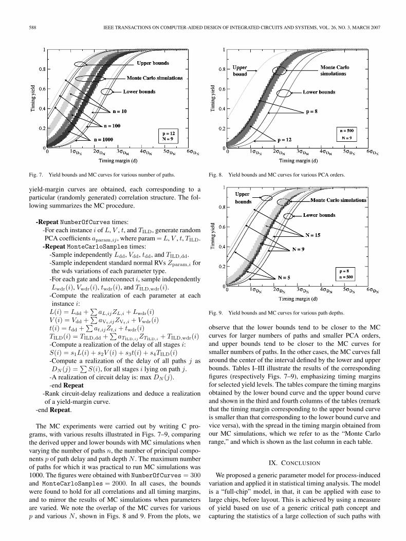
588 IEEE TRANSACTIONS ON COMPUTER-AIDED DESIGN OF INTEGRATED CIRCUITS AND SYSTEMS, VOL. 26, NO. 3, MARCH 2007
Fig. 7. Yield bounds and MC curves for various number of paths.
yield-margin curves are obtained, each corresponding to aparticular (randomly generated) correlation structure. The fol-lowing summarizes the MC procedure.
-Repeat NumberOfCurves times:-For each instance i of L, V , t, and TILD, generate randomPCA coefficients aparam,ij , where param = L, V , t, TILD.
-Repeat MonteCarloSamples times:-Sample independently Ldd, Vdd, tdd, and TILD,dd.-Sample independent standard normal RVs Zparam,i forthe wds variations of each parameter type.
-For each gate and interconnect i, sample independentlyLwdr(i), Vwdr(i), twdr(i), and TILD,wdr(i).
-Compute the realization of each parameter at eachinstance i:L(i) = Ldd +
∑aL,ijZL,i + Lwdr(i)
V (i) = Vdd +∑
aVt,ijZVt,i + Vwdr(i)t(i) = tdd +
∑at,ijZt,i + twdr(i)
TILD(i) = TILD,dd +∑
aTILD,ijZTILD,i
+ TILD,wdr(i)-Compute a realization of the delay of all stages i:S(i) = s1L(i) + s2V (i) + s3t(i) + s4TILD(i)-Compute a realization of the delay of all paths j asDN (j) =
∑S(i), for all stages i lying on path j.
-A realization of circuit delay is: max DN (j).-end Repeat
-Rank circuit-delay realizations and deduce a realizationof a yield-margin curve.
-end Repeat.
The MC experiments were carried out by writing C pro-grams, with various results illustrated in Figs. 7–9, comparingthe derived upper and lower bounds with MC simulations whenvarying the number of paths n, the number of principal compo-nents p of path delay and path depth N . The maximum numberof paths for which it was practical to run MC simulations was1000. The figures were obtained with NumberOfCurves = 300and MonteCarloSamples = 2000. In all cases, the boundswere found to hold for all correlations and all timing margins,and to mirror the results of MC simulations when parametersare varied. We note the overlap of the MC curves for variousp and various N , shown in Figs. 8 and 9. From the plots, we
Fig. 8. Yield bounds and MC curves for various PCA orders.
Fig. 9. Yield bounds and MC curves for various path depths.
observe that the lower bounds tend to be closer to the MCcurves for larger numbers of paths and smaller PCA orders,and upper bounds tend to be closer to the MC curves forsmaller numbers of paths. In the other cases, the MC curves fallaround the center of the interval defined by the lower and upperbounds. Tables I–III illustrate the results of the correspondingfigures (respectively Figs. 7–9), emphasizing timing marginsfor selected yield levels. The tables compare the timing marginsobtained by the lower bound curve and the upper bound curveand shown in the third and fourth columns of the tables (remarkthat the timing margin corresponding to the upper bound curveis smaller than that corresponding to the lower bound curve andvice versa), with the spread in the timing margin obtained fromour MC simulations, which we refer to as the “Monte Carlorange,” and which is shown as the last column in each table.
IX. CONCLUSION
We proposed a generic parameter model for process-inducedvariation and applied it in statistical timing analysis. The modelis a “full-chip” model, in that, it can be applied with ease tolarge chips, before layout. This is achieved by using a measureof yield based on use of a generic critical path concept andcapturing the statistics of a large collection of such paths with

NAJM et al.: YIELD MODEL FOR INTEGRATED CIRCUITS AND ITS APPLICATION TO TIMING ANALYSIS 589
TABLE ICOMPARISON OF MC RESULT WITH THE DERIVED BOUNDS FOR
DIFFERENT VALUES OF THE NUMBER OF CRITICAL PATHS n
TABLE IICOMPARISON OF MC RESULTS WITH THE DERIVED BOUNDS FOR
DIFFERENT VALUES OF THE PCA ORDER p
a model of within-die correlations based on PCA. This resultsin a methodology, whereby one can select the right settingof the transistor parameters to be used in simulation or intraditional timing analysis in order to verify the performancewhile guaranteeing a certain desired yield.
APPENDIX
We conducted a series of experiments to substantiate the va-lidity of the generic-path model in the context of circuit-timinganalysis. The accuracy of the generic-path model was verifiedby comparing the timing results from a standard direct STA-based MC analysis with a generic-path-based MC analysis.
Our standard MC experiments are carried out using the SSTAcapabilities in an industrial STA framework. This includes acomprehensive library characterization process to model vari-ation for the significant process parameters affecting delay.
TABLE IIICOMPARISON OF MC RESULTS WITH THE DERIVED BOUNDS FOR
DIFFERENT VALUES OF PATH DEPTH N
The MC capability in this framework works by first generatingthe systematic variation profiles (or spatial maps) for a set ofartificial dies. These profiles are generated using the PCA forthe process parameter that exhibits spatial correlation (chan-nel length). The mathematically generated population of diesmodels the parameter variations that would be seen after manu-facturing. Through prior experimentation, we have determinedthat 800 dies (MC samples) provide an acceptable accuracy forSSTA purposes. Depending on the location of the cell withineach die sample, a WDS is calculated for each cell. Hence, acell that falls within a high-Le region of the die would be slowerthan nominal. The WDR offsets are generated using a Gaussianrandom number generator. STA is then carried out for each ofthe generated dies using cell delays that are modified dependingon the offsets. The stage delay (driver input to receiver input)was calculated as
delay = nominal_delay(input slope, cload)
+ wds_offset × sensitivitywds(input slope, cload)
+ wdr_offset × sensitivitywdr(input slope, cload).
In the equation, sensitivitywds and sensitivitywdr are obtainedfrom the variation-aware library models. Path delays are mea-sured as the difference in arrival times between a capture flopdata pin and a launch flop clock pin (over one-cycle paths).Path delay for the longest path is stored for each of the diesand data from the STA runs for all dies was used to generate adistribution.
For the generic-path-based MC analysis, the generic path wascreated out of an alternating sequence of inverters and NAND2swith a total delay equal to the cycle time T of the design.Each die sample was divided into a grid with the dimensionof each grid square set to the distance at which the systematic

590 IEEE TRANSACTIONS ON COMPUTER-AIDED DESIGN OF INTEGRATED CIRCUITS AND SYSTEMS, VOL. 26, NO. 3, MARCH 2007
TABLE IVDESIGN 1: 19 264 CELLS
TABLE VDESIGN 2: 131 897 CELLS
correlation would drop to 0.98. That is, all devices within eachgrid square are highly correlated. An identical generic pathis assigned to each grid square. Essentially, this generic pathrepresents all critical paths within the grid square. For each diesample (or spatial profile), a delay analysis is carried out for theset of generic paths with the variation-aware delay for the pathcalculated as shown above. The maximum path delay deter-mines the critical delay for that die sample. The overall distrib-ution is obtained by combining the results from all die samples.
Tables IV and V compare the maximum path-delay dis-tribution obtained from the STA-based MC analysis to thatobtained from the generic-path-based MC run. These resultswere obtained for two industrial designs at two successivetechnology nodes. In these tables, the percentage error is de-fined as 100 ∗ (Generic_Path—Direct_MC)/Direct_MC. Thesetables corroborate the validity of the generic-path model and itsusefulness in an actual design cycle.
ACKNOWLEDGMENT
The authors would like to thank C. Amin and K. Killpack ofIntel’s Strategic CAD Labs for the extensive help provided andalso the anonymous reviewers of this paper for their commentsand suggestions which helped improve this paper.
REFERENCES
[1] S. W. Director, W. Maly, and A. J. Strojwas, VLSI Design Manufacturingfor Yield Enhancement. Boston, MA: Kluwer, 1990.
[2] W. Moore, W. Maly, and A. Strojwas, Eds., Yield Modelling and DefectTolerance in VLSI, Bristol, U.K.: Adam Hilger, 1987.
[3] K. Bernstein, K. M. Carrig, C. M. Durham, P. R. Hansen, D. Hogenmiller,E. J. Nowak, and N. J. Rohrer,High Speed CMOSDesign Styles. Boston,MA: Kluwer, 1999.
[4] J. B. Khare and W. Maly, From Contamination to Defects, Faults, andYield Loss. Boston, MA: Kluwer, 1996.
[5] M. Eisele, J. Berthold, D. Schmitt-Landsiedel, and R. Mahnkopf, “Theimpact of intra-die device parameter variations on path delays and on thedesign for yield of low voltage digital circuits,” IEEE Trans. Very LargeScale Integr. (VLSI) Syst., vol. 5, no. 4, pp. 360–368, Dec. 1997.
[6] A. Gattiker, S. Nassif, R. Dinakar, and C. Long, “Timing yield estimationfrom static timing analysis,” in Proc. IEEE Int. Symp. Quality Electron.Des., San Jose, CA, Mar. 26–28, 2001, pp. 437–442.
[7] S. R. Nassif, Statistical Worst-Case Analysis for Integrated Circuits Sta-tistical Approach to VLSI, ser. Advances in CAD for VLSI, vol. 8,
S. W. Director and W. Maly, Eds. Amsterdam, The Netherlands: North-Holland, 1994.
[8] K. Singhal and V. Visvanathan, “Statistical device models for worst casefiles and electrical test data,” IEEE Trans. Semicond. Manuf., vol. 12,no. 4, pp. 470–484, Nov. 1999.
[9] D. Boning and S. Nassif, “Models of process variations in device andinterconnect,” in Design of High-Performance Microprocessor Circuits,A. Chandrakasan, W. J. Bowhill, and F. Fox, Eds. New York: IEEEPress, 2001, ch. 6.
[10] L. Mizrukhin, J. Huey, and S. Mehta, “Prediction of product yield distri-butions from wafer parametric measurements of CMOS circuits,” IEEETrans. Semicond. Manuf., vol. 5, no. 2, pp. 88–93, May 1992.
[11] K. K. Low and S. W. Director, “A new methodology for the design cen-tering of IC fabrication processes,” IEEE Trans. Comput.-Aided DesignIntegr. Circuits Syst., vol. 10, no. 7, pp. 895–903, Jul. 1991.
[12] R. W. Dutton and A. J. Strojwas, “Perspectives on technology andtechnology-driven CAD,” IEEE Trans. Comput.-Aided Design Integr.Circuits Syst., vol. 19, no. 12, pp. 1544–1560, Dec. 2000.
[13] S. R. Nassif, “Within-chip variability analysis,” in Proc. IEEEInt. Electron. Devices Meeting, San Francisco, CA, Dec. 6–9, 1998,pp. 283–286.
[14] B. E. Stine, D. S. Boning, and J. E. Chung, “Analysis and decompositionof spatial variation in integrated circuit processes and devices,” IEEETrans. Semicond. Manuf., vol. 10, no. 1, pp. 24–41, Feb. 1997.
[15] V. Mehrotra, S. L. Sam, D. Boning, A. Chandrakasan, R. Vallishayee,and S. Nassif, “A methodology for modeling the effects of systematicwithin-die interconnect and device variations on circuit performance,” inProc. ACM/IEEE Des. Autom. Conf., Los Angeles, CA, Jun. 5–9, 2000,pp. 172–175.
[16] J. A. G. Jess, K. Kalafala, W. R. Naidu, R. H. J. M. Otten, andC. Visweswariah, “Statistical timing for parametric yield prediction ofdigital integrated circuits,” in Proc. ACM/IEEE Des. Autom. Conf.,Anaheim, CA, Jun. 2–6, 2003, pp. 932–937.
[17] C. Visweswariah, “Death, taxes and failing chips,” in Proc. ACM/IEEEDes. Autom. Conf., Anaheim, CA, Jun. 2–6, 2003, pp. 343–347.
[18] A. Agarwal, D. Blaauw, V. Zolotov, and S. Vrudhula, “Computation andrefinement of statistical bounds on circuit delay,” in Proc. ACM/IEEEDes.Autom. Conf., Anaheim, CA, Jun. 2–6, 2003, pp. 348–353.
[19] A. Agarwal, D. Blaauw, and V. Zolotov, “Statistical timing analysisfor intra-die process variations with spatial correlations,” in Proc.IEEE/ACM Int. Conf. Comput.-Aided Des., San Jose, CA, Nov. 9–13,2003, pp. 900–907.
[20] H. Chang and S. S. Sapatnekar, “Statistical timing analysis consider-ing spatial correlations using a single PERT-like traversal,” in Proc.IEEE/ACM Int. Conf. Comput.-Aided Des., San Jose, CA, Nov. 9–13,2003, pp. 621–625.
[21] A. Devgan and C. Kashyap, “Block-based static timing analysiswith uncertainty,” in Proc. IEEE/ACM Int. Conf. Comput.-Aided Des.,San Jose, CA, Nov. 9–13, 2003, pp. 607–614.
[22] S. Bhardwaj, S. B. Vrudhula, and D. Blaauw, “Tau: Timing analysisunder uncertainty,” in Proc. IEEE/ACM Int. Conf. Comput.-Aided Des.,San Jose, CA, Nov. 9–13, 2003, pp. 615–620.
[23] K. A. Bowman and J. D. Meindl, “Impact of within-die parameter fluc-tuations on future maximum clock frequency distributions,” in Proc.IEEE Custom Integr. Circuits Conf., San Diego, CA, May 6–9, 2001,pp. 229–232.
[24] F. N. Najm and N. Menezes, “Statistical timing analysis based on a timingyield model,” in Proc. ACM/IEEE Des. Autom. Conf., San Diego, CA,Jun. 7–11, 2004, pp. 460–465.
[25] X. Bai, C. Visweswariah, P. N. Strenski, and D. J. Hathaway,“Uncertainty-aware circuit optimization,” in Proc. Des. Autom. Conf.,New Orleans, LA, Jun. 10–14, 2002, pp. 58–63.
[26] M. S. Srivastava, Methods of Multivariate Statistics. New York: Wiley-Interscience, 2002.
[27] J. M. Rabaey, Digital Integrated Circuits: A Design Perspective. UpperSaddle River, NJ: Prentice-Hall, 1996.
[28] Y. Liu, L. T. Pileggi, and A. J. Strojwas, “Model order-reduction of RC(L)interconnect including variational analysis,” in Proc. Des. Autom. Conf.,New Orleans, LA, Jun. 21–25, 1999, pp. 201–206.
[29] E. Acar, S. Nassif, Y. Liu, and L. T. Pileggi, “Time-domain simulationof variational interconnect models,” in Proc. IEEE Int. Symp. QualityElectron. Des., San Jose, CA, Mar. 18–21, 2002, pp. 419–424.
[30] E. Malavasi, S. Zanella, M. Cao, J. Uschersohn, M. Misheloff, andC. Guardiani, “Impact analysis of process variability on clock skew,” inProc. IEEE Int. Symp. Quality Electron. Des., San Jose, CA, Mar. 18–21,2002, pp. 129–132.
NAJM et al.: YIELD MODEL FOR INTEGRATED CIRCUITS AND ITS APPLICATION TO TIMING ANALYSIS 591
[31] A. Papoulis, Probability, Random Variables, and Stochastic Processes.New York: McGraw-Hill, 1984.
[32] S. Boyd and L. Vandenberghe, Convex Optimization. New York:Cambridge Univ. Press, 2004. [Online]. Available: http://www.stanford.edu/~boyd/cvxbook.html
Farid N. Najm (S’85–M’89–SM’96–F’03) receivedthe B.E. degree in electrical engineering fromthe American University of Beirut (AUB), Beirut,Lebanon, in 1983 and the M.S. and Ph.D. degrees inelectrical and computer engineering (ECE) from theUniversity of Illinois at Urbana-Champaign (UIUC),in 1986 and 1989, respectively.
From 1989 to 1992, he worked with Texas Instru-ments, Dallas. Then, he joined the ECE Departmentat UIUC as an Assistant Professor and eventuallybecame an Associate Professor in 1997. In 1999, he
joined the ECE Department at the University of Toronto, Toronto, ON, Canada,where he is currently a Professor and a Vice Chair of ECE. He has coauthoredthe text Failure Mechanisms in Semiconductor Devices, 2nd ed. (Wiley, 1997).His research is on computer-aided design (CAD) for integrated circuits, withan emphasis on circuit level issues related to power dissipation, timing, andreliability.
Dr. Najm is an Associate Editor for the IEEE TRANSACTIONS ON
COMPUTER-AIDED DESIGN OF INTEGRATED CIRCUITS AND SYSTEMS. Hereceived the IEEE Transactions on CAD Best Paper Award in 1992, the NSFResearch Initiation Award in 1993, the NSF CAREER Award in 1996, andwas an Associate Editor for the IEEE TRANSACTIONS ON VERY LARGE
SCALE INTEGRATION (VLSI) SYSTEMS from 1997 to 2002. He served as aGeneral Chairman for the 1999 International Symposium on Low-Power Elec-tronics and Design (ISLPED-99) and as a Technical Program Cochairman forISLPED-98. He has also served on the technical committees of ICCAD, DAC,CICC, ISQED, and ISLPED.
Noel Menezes (S’93–M’95) received the B.Eng. de-gree from Maharaja Sayajirao University, Baroda,India, and the M.S. and Ph.D. degrees from theUniversity of Texas, Austin.
He is currently the Manager with the Core CADresearch group at Intel’s Strategic CAD Labs inHillsboro, OR. In the past, he has worked on in-terconnect optimization algorithms, clock tree syn-thesis, gate-delay engines, statistical static timinganalysis, and inductance extraction. Results of hisresearch have been applied in the design of various
IBM and Intel microprocessors. He is also a Coinventor of the popular Theveningate-driver model for resistive interconnects which is used in most industrytiming analyzers. He has been a member of the technical program committeefor most major CAD conferences.
Imad A. Ferzli (S’00) received the B.E. degree incomputer and communications engineering from theAmerican University of Beirut, Beirut, Lebanon, in2001, and the M.A.Sc. degree in electrical and com-puter engineering from the University of Toronto,Toronto, ON, Canada, in 2004. He is currently work-ing toward the Ph.D. degree at the University ofToronto.
He interned with Magma Design Automation,Eindhoven, The Netherlands, in the summer of 2006.His research interests include CAD development for
design for manufacturability and process variations, power grid verification anddesign, timing analysis, and yield modeling and prediction.
Mr. Ferzli is a Student Member of the Semiconductor Research Corporation.