a8517: wide input voltage, fault tolerant, …/media/files/datasheets/a8517...register sda scl vovp...
TRANSCRIPT

The A8517 is a programmable multi-output LED driver, which can be used for a variety of LED driver applications. It integrates a current-mode boost converter with internal power switch and 10 current sinks. The IC operates from 4.5 to 36 V, and is able to withstand up to 40 V load-dump conditions encountered in automotive systems.
The I2C interface allows the user to set the LED currents individually, up to 60 mA per LED channel. Adjacent channels may be combined to drive higher-current LED strings. The PWM dimming duty cycle is independently controlled for each LED channel, and each channel can be enabled/disabled independently if needed.
This flexibility makes the A8517 a single solution for a wide range of LED applications, in some cases offering the ability to replace two or more LED driver ICs with a single device.
A8517-DS, Rev. 11MCO-0000140
• AEC-Q100 qualified• Wide input voltage range of 4.5 to 36 V• Operates down to 3.9 V (VIN falling) for idle stop, and up
to 40 V for load dump• Integrated boost converter with DMOS switch and OVP
protection up to 39 V• 10 fully integrated LED current sinks, with individually
programmable current up to 60 mA per channel• I2C™ interface for programming LED current, PWM
dimming, and various protection thresholds per channel• Ability to drive multiple loads from a single IC• Extensive PWM dimming (up to 10,000:1 at 100 Hz),
individually programmable for each channel• Extensive diagnostics and fault reporting
Wide Input Voltage, Fault Tolerant, Independently Controlled Multi-Channel LED Driver with I2C Interface
PACKAGE:
Typical Application Drawing
Not to scale
A8517
Continued on the next page…
Continued on the next page…
APPLICATIONS:Automotive:• Infotainment• Cluster• Center-stack lighting• Head-up display (HUD)• Daytime running lights (DRL)
COUT
CVDD
OVP
Q CQ11
L1
INS
VDD LED1
LED2PAD
LED10
RFSET
RADDR
CZ
RZ
GATE
EN
FLAG
VIN (4.5 to 36 V)
SW
COMP
PGND
AGND
FSET/SYNC
CIN
VC
SDA
SCL
ADDR
A8517
D1
Optional
VOUT
ExternalSynchronization
RSENSE
VIN
GPO1 GPO2
Status /Interrupt
I2C Interface
A
A
AExternal pull-up voltage, orconnected to VDD
B
B GNDCP
FEATURES AND BENEFITS DESCRIPTION
October 24, 2017
28-pin TSSOP with exposed thermal pad (suffix LP)

Wide Input Voltage, Fault Tolerant, Independently Controlled Multi-Channel LED Driver with I2C InterfaceA8517
2Allegro MicroSystems, LLC115 Northeast CutoffWorcester, Massachusetts 01615-0036 U.S.A.1.508.853.5000; www.allegromicro.com
The control loop is optimized to achieve very high dimming ratios using only PWM control, to react smoothly to supply voltage transients and step changes, and to eliminate night flash in display backlight applications when starting up at very low PWM duty cycle.
The A8517 detects and protects against a wide variety of fault conditions, and two-way communication allows fault status to be reported. It provides protection against output short and overvoltage, open or shorted diode, open or shorted LED pin, shorted boost switch or inductor, and IC overtemperature. A dual cycle-by-cycle current limit protects the internal switch against switch overcurrent. If required, the IC can drive an external PFET as an input-disconnect switch that is triggered by integrated current sense.
• Thermal warning and derating of LED current at higher temperatures
• Buffered PWM dimming control for all channels to facilitate localized dimming applications
• Polyphase PWM dimming: LED currents staggered to reduce light flickering and input ripple current
• Synchronize boost switching frequency: 400 kHz to 2.3 MHz to allow operation below or above the AM band
• Programmable frequency dithering to reduce EMI• Typical LED current accuracy of 0.7%, and LED-to-LED
matching accuracy of 0.8%• Protection Features
Open/shorted LED pin detection Programmable LED string short detection Open/shorted external components (including boost inductor, Schottky diode, FSET resistor and so forth)
Input overcurrent protection against output to GND short
FEATURES AND BENEFITS (continued)
DESCRIPTION (continued)
SELECTION GUIDE
Part NumberOperating Ambient Temperature Range
TA (°C)Package Packing [1] Leadframe
Plating
A8517KLPTR-T –40 to 125 28-pin TSSOP with exposed thermal pad 4000 pieces per 13-in. reel 100% matte tin
[1] Contact Allegro™ for additional packing options.
Cycle-by-cycle switch current limit Overtemperature, and output overvoltage and undervoltage protection
Table of ContentsFeatures and Benefits 1Description 1Applications 1Package 1Typical Application Drawing 1Selection Guide 2Specifications 3
Absolute Maximum Ratings 3Thermal Characteristics 3
Functional Block Diagram 4Pinout Diagram and Terminal List Table 5Electrical Characteristics 6Characteristic Performance 9Fault Handling 14
Input Overcurrent Protection 14Switch Overcurrent Protection 15LED String Open Fault Detection 15Protection Against Open/Missing BOOST Diode 16
Functional Description 17Enabling the IC 17PWM Dimming 18Output Current and Voltage 22Boost Frequency Dithering 22
Polyphase Grouping 23Boost Output Voltage Regulation 24Output Hysteresis 24Soft Start Timing 24Input Disconnect Switch 24System Failure Detection and Protection 26Fault Handling 27
Application Information 31Package Outline Drawing 38Appendix A: Programming Information A-1
I2C Interface Description A-2Timing Considerations A-2I2C Command Write to the A8517 A-3I2C Command Read from the A8517 A-4Order of Reading and Writing Registers A-4Dealing with Incomplete Transmission A-4Register Map A-6Register Field Reference A-8
Appendix B: Feedback Loop Calculations B-1Power Stage Transfer Function B-1Output to Control Transfer Function B-2Stabilizing the Closed Loop System B-4Measuring Feedback Loop Gain, Phase Margin B-7
Wide Input Voltage, Fault Tolerant, Independently Controlled Multi-Channel LED Driver with I2C InterfaceA8517
3Allegro MicroSystems, LLC115 Northeast CutoffWorcester, Massachusetts 01615-0036 U.S.A.1.508.853.5000; www.allegromicro.com
THERMAL CHARACTERISTICS: May require derating at maximum conditions; see application informationCharacteristic Symbol Test Conditions [2] Value Unit
Package Thermal Resistance RθJA On 4-layer PCB based on JEDEC standard 28 °C/W
[2] Additional thermal information available on the Allegro website.
ABSOLUTE MAXIMUM RATINGS [1]
Characteristic Symbol Notes Rating UnitLEDx Pins VLEDx –0.3 to 42 V
F L A G , GPO2, and OVP Pins –0.3 to 42 V
EN, VIN, INS, and GATE Pins INS and GATE pins should not exceed VIN by more than 0.4 V –0.3 to 40 V
SW Pin VSWContinuous –0.6 to 42 V
t < 50 ns –1.0 to 46 V
VDD, FSET/SYNC, COMP, GPO1, SDA, SCL, and ADDR Pins –0.3 to 5.5 V
Operating Ambient Temperature TA K temperature range –40 to 125 °C
Maximum Junction Temperature TJ(max) 150 °C
Storage Temperature Tstg –65 to 150 °C
[1] Operation at levels beyond the ratings listed in this table may cause permanent damage to the device. The Absolute Maximum ratings are stress ratings only, and functional operation of the device at these or any other conditions beyond those indicated in the Electrical Characteristics table is not implied. Exposure to Absolute Maximum-rated conditions for extended periods may affect device reliability.
SPECIFICATIONS

Wide Input Voltage, Fault Tolerant, Independently Controlled Multi-Channel LED Driver with I2C InterfaceA8517
4Allegro MicroSystems, LLC115 Northeast CutoffWorcester, Massachusetts 01615-0036 U.S.A.1.508.853.5000; www.allegromicro.com
Functional Block Diagram
100 kΩ
Fault
Current Sense
Diode Open Sense
OVP Sense
TSD
Open /Short LED Detect
Enable
Regulator UVLO
GATE
VDD
VIN
SW
AGND
FSET /SYNC
BandgapReference
Driver Circuit
Startup/Shutdown
OscillatorInternalVCC
InternalVCC
VOVP REG
OVP
LED1
LED10
...
VREF
EN
AGND
Register
SDA
SCL
VOVP
10 µA
REG
ADDR
FLAG
I2C Interface
COMP
VREG
PWM1 to PWM10
ISET1 to ISET10
LED Driver
COMP
Fault Status
INS OCP
`
`
PGND
GPO1
GPO2MUX
Selector
COMP
PAD
+
–
+
–
+
–
+
–
+
–
+
–
10
10 10
10
OCP

Wide Input Voltage, Fault Tolerant, Independently Controlled Multi-Channel LED Driver with I2C InterfaceA8517
5Allegro MicroSystems, LLC115 Northeast CutoffWorcester, Massachusetts 01615-0036 U.S.A.1.508.853.5000; www.allegromicro.com
Package LP, 28-Pin TSSOP Pinout DiagramTerminal List Table
Name Number Function
ADDR 25 This pin has 4 levels that allow the user to set up to 4 physical IC addresses based on the voltage level. Connect a resistor to GND to set the voltage level.
AGND 7, 15 Analog ground; connect all noise-sensitive components (especially for COMP) to this quiet ground, and connect to thermal pad.
COMP 6 Output of error amplifier and compensation node; connect a type-2 feedback network from this pin to AGND for control loop compensation.
EN 4 Enable for the A8517; IC stays in shutdown mode as long as EN = VEN(L) , enables the part when connected to VEN(H) or to VIN .
F L A G 9 This active-low, open-drain pin is used to indicate that system attention is required, such as during startup or a fault condition. Connect a resistor with a value from 10 to 100 kΩ between this pin and the target logic level voltage.
FSET/SYNC 5 Frequency/synchronization pin; a resistor, RFSET , from this pin to GND sets the switching frequency, and this pin can also be used to synchronize to an external switching frequency.
GATE 1 Gate driver for optional external PMOS input disconnect switch, that in the event of a fault (such as output shorted to GND) is turned off by this pin being pulled high (turning off input supply); if not used, this pin should be left open.
GPO1 22 General purpose open-drain output 1, programmable by internal register.
GPO2 21 General purpose open-drain output 2, programmable by internal register.
INS 2 Input current sense, used together with VIN pin to detect input overcurrent fault; if not used, this pin should be tied to VIN.
LEDx10, 11, 12, 13, 14, 16,
17, 18, 19, 20
LED current sink channels 1 through 10. Up to 60 mA per channel. Any unused LEDx pin should be connected to GND through a 4.7 kΩ resistor.
OVP 27 Connect this pin to output voltage VOUT to provide output Overvoltage Protection (OVP) and Undervoltage Protection (UVP).
PAD –Exposed pad of the package providing enhanced thermal dissipation. This pad must be connected to the ground plane(s) of the PCB with at least 8 vias, directly in the pad, and AGND and PGND pins must be connected to this ground pad on the PCB.
PGND 26 Power ground for internal NMOS switching device; connect this pin to ground terminal of output ceramic capacitor(s) and to thermal pad.
SCL 24 I2C clock signal.
SDA 23 I2C data signal.
SW 28 The drain of the internal NMOS switch of the boost converter.
VDD 8 Output of internal LDO; connect a 0.47 µF decoupling capacitor between this pin and AGND.
VIN 3 Input power to the A8517.
GATE
INS
VIN
EN
FSET/SYNC
COMP
AGND
VDD
FLAG
LED1
LED2
LED3
LED4
LED5
SW
OVP
PGND
ADDR
SCL
SDA
GOP1
GPO2
LED10
LED9
LED8
LED7
LED6
AGND
1
2
3
4
5
6
7
8
9
10
11
12
13
14
28
27
26
25
24
23
22
21
20
19
18
17
16
15
PAD
PINOUT DIAGRAM AND TERMINAL LIST TABLE

Wide Input Voltage, Fault Tolerant, Independently Controlled Multi-Channel LED Driver with I2C InterfaceA8517
6Allegro MicroSystems, LLC115 Northeast CutoffWorcester, Massachusetts 01615-0036 U.S.A.1.508.853.5000; www.allegromicro.com
Characteristic Symbol Test Conditions Min. Typ. Max. UnitINPUT VOLTAGE
Input Voltage Range VIN Measured at the VIN pin 4.5 − 36 V
VIN Pin UVLO Start VINUV(ON) VIN rising − − 4.35 V
VIN Pin UVLO Stop VINUV(OFF) VIN falling − − 3.90 V
VIN Pin UVLO Hysteresis VINUV(HYS) − 400 − mV
INPUT CURRENT
Input Quiescent Current IQMeasured at the VIN pin, EN = VEN(H) , fSW = 2 MHz no load − 15 − mA
Input Sleep Supply Current IQSLEEPSum of VIN and INS pin currents, VIN = VINS = 16 V, VEN = 0 V − 3.5 10.0 µA
EN (ENABLE) PIN
EN Input Logic Level – Low VEN(L) 4.5 V < VIN < 36 V − − 0.4 V
EN Input Logic Level – High VEN(H) 4.5 V < VIN < 36 V 1.5 − − V
EN Internal Pull-Down Resistance RENPD − 100 − kΩ
ERROR AMPLIFIERSource Current IEA(SRC) VCOMP = 0.75 V, VLEDx = 0.3 V − –200 − µA
Sink Current IEA(SINK) VCOMP = 0.75 V. VLEDx = 1.5 V − +200 − µA
COMP Pin Internal Pull-Down Resistance RCOMPPD During startup and shutdown − 2000 − Ω
OUTPUT OVERVOLTAGE AND UNDERVOLTAGE PROTECTION
Overvoltage ThresholdVOVPMIN OVP register = xxx0 0000 7.5 8 8.5 V
VOVPMAX OVP register = xxx1 1111 38 39 40 V
Overvoltage Step Size VOVPSTEP − 1.0 − V
Undervoltage ThresholdVUVPMIN OVP register = xxx0 0000 − 0.49 − V
VUVPMAX OVP register = xxx1 1111 − 2.5 − V
OVP Pin Input Impedance ROVP VOVP = 20 V, EN = VEN(H) − 800 − kΩ
OVP Leakage Current IOVPLKG VOVP =16 V, EN = VEN(L) − 0.1 1 µA
Secondary Overvoltage Protection VOVP(sec) Measured at SW pin − 44 − V
Continued on the next page…
ELECTRICAL CHARACTERISTICS [1]: Valid at VIN = 16 V , TA = 25°C, EN = VEN(H) , indicates specifications valid across the full operating temperature range with TA = TJ = –40°C to 125°C and with typical specifications at TA = 25°C; unless oth-erwise specified

Wide Input Voltage, Fault Tolerant, Independently Controlled Multi-Channel LED Driver with I2C InterfaceA8517
7Allegro MicroSystems, LLC115 Northeast CutoffWorcester, Massachusetts 01615-0036 U.S.A.1.508.853.5000; www.allegromicro.com
Continued on the next page…
Characteristic Symbol Test Conditions Min. Typ. Max. UnitBOOST SWITCHSwitch On-Resistance RDS(ON) ISW = 0.750 A, VIN = 16 V − 220 350 mΩ
Switch Leakage Current ISWLKG
VSW = 16 V, EN = VEN(L) , TA = TJ = –40°C to 85°C − 0.1 10 µA
VSW = 16 V, EN = VEN(L) , TA = TJ = 125°C − 3 − µA
Cycle-by-Cycle Switch Current Limit ISW(LIM) 3.6 4.2 4.8 A
Secondary Switch Current Limit [2] ISWLIM(sec)Higher than maximum ISW(LIM) at any condition (A8517 latches when detected) 5.6 7.0 − A
Minimum Switch On-Time tSWONTIME RFSET = 10 kΩ − 85 120 ns
Minimum Switch Off-Time tSWOFFTIME RFSET = 10 kΩ − 55 85 ns
SWITCHING FREQUENCY
Boost Stage Switching Frequency fSW
RFSET = 10 kΩ 1.8 2 2.2 MHz
RFSET = 20.1 kΩ − 1 − MHz
RFSET = 40.6 kΩ − 500 − kHz
FSET/SYNC Pin Voltage VFSETSYNC RFSET = 10 kΩ − 1.00 − V
SYNCHRONIZATIONSynchronized Boost Stage Switching
Frequency fSW_SYNC 400 − 2300 kHz
Synchronization Input Minimum Off-Time tSYNCPWOFF 150 − − ns
Synchronization Input Minimum On-Time
tSYNCPWON 150 − − ns
Synchronization Input Logic – Low VSYNCON(L) − − 0.4 V
Synchronization Input Logic – High VSYNCON(H) 2 − − V
LED CURRENT SINKS
LEDx Accuracy (Average) ErrLEDx Measured at ILEDMAX (maximum LED current) − 0.7 3 %
LEDx Matching ΔILEDxCompared to average ILEDx , measured at ILEDMAX
− 0.8 3 %
LEDx Regulation Voltage VREG ISET register = xx11 1111 − 0.85 1.0 V
ILEDx Step Size ISETSTEP Total 64 steps 0.9 1 1.1 mA
Maximum LEDx Current (Average) ILEDMAX ISET register = xx11 1111 62 64 66 mA
Minimum LEDx Current ILEDMIN ISET register = xx00 0000 − 1 − mA
LEDx Short-Detect Threshold VLED_SDShort-Detect register = 000 − 12 − V
Short-Detect register = 111 − 5 − V
INTERRUPTS (FLAG, GPO1 AND GPO2 PINS)
Pin Pull-Down Voltage Fault / Interrupt condition asserted, pull-up current = 0.5 mA − − 0.4 V
Pin Leakage Current Fault / Interrupt condition cleared, pull-up to 3.6 V − − 1 µA
ELECTRICAL CHARACTERISTICS [1] (continued): Valid at VIN = 16 V , TA = 25°C, EN = VEN(H) , indicates specifications valid across the full operating temperature range with TA = TJ = –40°C to 125°C and with typical specifications at TA = 25°C; unless otherwise specified

Wide Input Voltage, Fault Tolerant, Independently Controlled Multi-Channel LED Driver with I2C InterfaceA8517
8Allegro MicroSystems, LLC115 Northeast CutoffWorcester, Massachusetts 01615-0036 U.S.A.1.508.853.5000; www.allegromicro.com
Characteristic Symbol Test Conditions Min. Typ. Max. UnitINTERNAL MASTER CLOCK
Master Clock Period TCLK 120 150 180 ns
Master Clock Temperature Deviation [2] DTCLK TCLK change over temperature range –2.5 – 2.5 %
INPUT DISCONNECT
GATE Pin Sink Current IGSINKVGATE = VIN , no input overcurrent fault tripped − 115 − µA
GATE Pin Source Current IGSOURCEVGATE = VIN – 5V, input overcurrent fault tripped − –6 − mA
GATE Voltage at Off VGSOFF EN = VEN(L) , or overcurrent fault occurred − VIN − V
GATE Voltage at On VGSONGate-to-source voltage when gate is on, measured as VIN – VGATE
5 − 8 V
GATE Pin Leakage Current IGLKG EN = VEN(L) , VGATE = VIN − − 1 µA
INS Pin Sink Current IINSSINK − 20 − µA
INS Trip Point VINSTRIP Measured between VIN and INS 90 105 120 mV
INS Trip Detection Time [2] tINSTRIP Sensed voltage, VIN – VINS = 160 mV − 2 − µs
THERMAL PROTECTION (TSD)Thermal Shutdown Threshold [2]
TSD Temperature rising 155 170 − °C
Thermal Shutdown Hysteresis [2]TSDHYS − 20 − °C
Thermal Warning Threshold TSDWARNTemperature rising, measured as difference from TSD − 20 − °C
I2C INTERFACELogic Input (SDA, SCL) - Low VSCL(L) − − 0.8 V
Logic Input (SDA, SCL) - High VSCL(H) 2.3 − − V
Logic Input Hysteresis VI2CIHYS − 150 − mV
Logic Input Current II2CI –1 − 1 µA
Output Voltage SDA VI2COut(L) SDA = low, pull-up current = 2.5 mA − − 0.4 V
Output Leakage SDA II2CLKG EN = low, pull-up to 5.5 V − − 1 µA
SCL Clock Frequency fCLK − − 400 kHz
ADDR PINVoltage Level for Address 100,0000 VADDLEVEL1 ADDR connected to GND 0 − 0.5 V
Voltage Level for Address 101,0000 VADDLEVEL2 RADDR = 110 kΩ from ADDR to GND 0.9 − 1.3 V
Voltage Level for Address 110,0000 VADDLEVEL3 RADDR = 210 kΩ from ADDR to GND 1.75 − 2.45 V
Voltage Level for Address 111,0000 VADDLEVEL4 ADDR connected to VDD pin or open 3.2 − 3.6 V
ADDR Pull-Up Current IADDR VADDR = 1 V 8.5 10 11.5 µA
INTERNAL REGULATORBias Supply Voltage VDD − 3.6 − V
[1] For input and output current specifications, negative current is defined as coming out of the node or pin (sourcing), positive current is defined as going into the node or pin (sinking).
[2] Ensured by design and characterization, not production tested.
ELECTRICAL CHARACTERISTICS [1] (continued): Valid at VIN = 16 V , TA = 25°C, EN = VEN(H) , indicates specifications valid across the full operating temperature range with TA = TJ = –40°C to 125°C and with typical specifications at TA = 25°C; unless otherwise specified

Wide Input Voltage, Fault Tolerant, Independently Controlled Multi-Channel LED Driver with I2C InterfaceA8517
9Allegro MicroSystems, LLC115 Northeast CutoffWorcester, Massachusetts 01615-0036 U.S.A.1.508.853.5000; www.allegromicro.com
CHARACTERISTIC PERFORMANCE
50
60
70
80
90
100
8 10 12 14 16 18 20
Effic
ienc
y, η
(%)
VIN (V)
Efficiency versus Input Voltage7 series LEDs, 10 parallel strings at 60 mA each
70
75
80
85
90
95
0.05 0.10 0.15 0.20 0.25 0.30 0.35 0.40 0.45 0.50 0.55 0.60
Total LED Current (A)
Efficiency versus Output Current
65
70
75
80
85
90
95
12 14 16 18 20 22 24 26 28 30
Efficiency versus Output Voltage
Effic
ienc
y, η
(%)
Effic
ienc
y, η
(%)
Effic
ienc
y, η
(%)
fSW = 400 kHz
fSW = 2 MHz
7 series LEDs, 10 parallel strings at 60 mA each
fSW = 400 kHz
fSW = 2 MHz
VIN = 12 V
10 parallel strings at 60 mA each 9 series LEDs, 8 parallel strings at 50 mA each, L1 = 47 µH
fSW = 400 kHz
fSW = 2 MHz
VIN = 12 V
4 seriesLEDS
5 seriesLEDS
6 seriesLEDS
7 seriesLEDS 8 series
LEDS 9 seriesLEDS
9 seriesLEDS
8 seriesLEDS
7 seriesLEDS
6 seriesLEDS
5 seriesLEDS
4 seriesLEDS
70
75
80
85
90
95
0 200 400 600 800 1000 1200 1400 1600 1800 2000 2200
Efficiency versus Switching Frequency
Output Voltage (V) Switching Frequency (kHz))
VIN = 12 V

Wide Input Voltage, Fault Tolerant, Independently Controlled Multi-Channel LED Driver with I2C InterfaceA8517
10Allegro MicroSystems, LLC115 Northeast CutoffWorcester, Massachusetts 01615-0036 U.S.A.1.508.853.5000; www.allegromicro.com
Test conditions:
LED strings = 10 parallel, 60 mA eachLEDs = 7 series each string LED VREG = 0.85 V VIN = 12 V VOUT hysteresis = 0.45 V Dimming PWM duty cycle = 100%Polyphase mode = on
Test conditions:
LED strings = 10 parallel, 30 mA eachLEDs = 7 series each string LED VREG = 0.85 V VIN = 12 V VOUT hysteresis = 0.45 V Dimming PWM duty cycle = 100%Polyphase mode = on
Test conditions:
LED strings = 10 parallel, 60 mA eachLEDs = 7 series each string LED VREG = 0.85 V VIN = 5.5 V VOUT hysteresis = 0.45 V Dimming PWM duty cycle = 0.02% at 200 Hz (5000:1)Polyphase mode = on
Test conditions:
LED strings = 10 parallel, 60 mA eachLEDs = 7 series each string LED VREG = 0.85 V VIN = 5.5 V VOUT hysteresis = 0.45 V Dimming PWM duty cycle = 0.02% at 200 Hz (5000:1)Polyphase mode = on
Startup Waveform at VIN = 12 V Dimming PWM Duty Cycle = 100%
Startup Waveform at VIN = 5.5 V Dimming PWM Duty Cycle = 100%
Scope traces:
C1 (Yellow) = VOUT (5 V/div) C2 (Red) = VSW (20 V/div) C4 (Green) = ILED (200 mA/div) Time scale = 20 ms/div
A8517 evaluation PCB:
L1 = 10 µH, COUT5 = 68 µF / 50 V polymer electrolytic, COUT4 = 2.2 µF / 50 V 1206 ceramic, RZ = 10 kΩ, CZ = 5.6 nF, CP = 120 pF
Scope traces:
C1 (Yellow) = VOUT (5 V/div) C2 (Red) = VSW (20 V/div) C4 (Green) = ILED (200 mA/div) Time scale = 20 ms/div
A8517 evaluation PCB:
L1 = 10 µH, COUT5 = 68 µF / 50 V polymer electrolytic, COUT4 = 2.2 µF / 50 V 1206 ceramic, RZ = 10 kΩ, CZ = 5.6 nF, CP = 120 pF
Scope traces:
C1 (Yellow) = VOUT (5 V/div) C2 (Red) = VSW (20 V/div) C4 (Green) = ILED (20 mA/div) Time scale = 20 ms/div
A8517 evaluation PCB:
L1 = 10 µH, COUT5 = 68 µF / 50 V polymer electrolytic, COUT4 = 2.2 µF / 50 V 1206 ceramic, RZ = 10 kΩ, CZ = 5.6 nF, CP = 120 pF
Scope traces:
C1 (Yellow) = VOUT (5 V/div) C2 (Red) = VSW (20 V/div) C4 (Green) = ILED (20 mA/div) Time scale = 20 ms/div
A8517 evaluation PCB:
L1 = 10 µH, COUT5 = 68 µF / 50 V polymer electrolytic, COUT4 = 2.2 µF / 50 V 1206 ceramic, RZ = 10 kΩ, CZ = 5.6 nF, CP = 120 pF
Thermal derating chart for LED=
Startup Waveform at VIN = 12 V Dimming PWM Duty Cycle = 0.02%
Startup Waveform at VIN = 5.5 V Dimming PWM Duty Cycle = 0.02%

Wide Input Voltage, Fault Tolerant, Independently Controlled Multi-Channel LED Driver with I2C InterfaceA8517
11Allegro MicroSystems, LLC115 Northeast CutoffWorcester, Massachusetts 01615-0036 U.S.A.1.508.853.5000; www.allegromicro.com
Test conditions:
LED strings = 10 parallel, 60 mA eachLEDs = 7 series each string LED VREG = 0.85 V VIN = 12 V VOUT hysteresis = 0.45 V Dimming PWM duty cycle = 2% at 200 HzPolyphase mode = on (each on at assigned time slot)
Test conditions:
LED strings = 10 parallel, 60 mA eachLEDs = 7 series each string VIN = 12 V Dimming PWM duty cycle = change from 2% to 0.02% at 200 Hz (PWM on-time change from 100 µs to 1 µs)Polyphase mode = on
Test conditions:
LED strings = 10 parallel, 60 mA eachLEDs = 7 series each string VIN = 12 V Dimming PWM duty cycle = change from 0.02% to 2% at 200 Hz (PWM on-time change from 1 µs to 100 µs)Polyphase mode = on
Test conditions:
LED strings = 10 parallel, 60 mA eachLEDs = 7 series each string VIN = 12 V Dimming PWM duty cycle = 2% at 200 HzPolyphase mode = off (all simultaneously on)
PWM Operation with Polyphase
Transient Response to Step-ChangeIn PWM Duty Cycle ( 2% to 0.02%)
Scope traces:
C1 (Yellow) = VOUT (5 V/div) C4 (Green) = ILED (200 mA/div) Time scale = 1 ms/div
A8517 evaluation PCB:
L1 = 10 µH, COUT5 = 68 µF / 50 V polymer electrolytic, COUT4 = 2.2 µF / 50 V 1206 ceramic, RZ = 10 kΩ, CZ = 5.6 nF, CP = 120 pF
Scope traces:
C1 (Yellow) = VOUT (5 V/div) C3 (Blue) = I2C clock (5 V/div) C4 (Green) = ILED (20 mA/div) Time scale = 10 ms/div
A8517 evaluation PCB:
L1 = 10 µH, COUT5 = 68 µF / 50 V polymer electrolytic, COUT4 = 2.2 µF / 50 V 1206 ceramic, RZ = 10 kΩ, CZ = 5.6 nF, CP = 120 pF
Scope traces:
C1 (Yellow) = VOUT (5 V/div) C3 (Blue) = I2C clock (5 V/div) C4 (Green) = ILED (20 mA/div) Time scale = 10 ms/div
A8517 evaluation PCB:
L1 = 10 µH, COUT5 = 68 µF / 50 V polymer electrolytic, COUT4 = 2.2 µF / 50 V 1206 ceramic, RZ = 10 kΩ, CZ = 5.6 nF, CP = 120 pF
Scope traces:
C1 (Yellow) = VOUT (5 V/div) C4 (Green) = ILED (200 mA/div) Time scale = 1 ms/div
A8517 evaluation PCB:
L1 = 10 µH, COUT5 = 68 µF / 50 V polymer electrolytic, COUT4 = 2.2 µF / 50 V 1206 ceramic, RZ = 10 kΩ, CZ = 5.6 nF, CP = 120 pF
PWM Operation without Polyphase
Transient Response to Step-ChangeIn PWM Duty Cycle ( 0.02% to 2%)
Period
PWM at 2% PWM at 0.02%
Thermal derating chart for LED=
PWM at 0.02% PWM at 2%
Period
Period / 10
Phase
1
Phase
2
Phase
3
Phase
4
Phase
5
Phase
6
Phase
7
Phase
8
Phase
9
Phase
10
Phase
1
Wide Input Voltage, Fault Tolerant, Independently Controlled Multi-Channel LED Driver with I2C InterfaceA8517
12Allegro MicroSystems, LLC115 Northeast CutoffWorcester, Massachusetts 01615-0036 U.S.A.1.508.853.5000; www.allegromicro.com
Test conditions:
LED strings = 10 parallel, 60 mA eachLEDs = 7 series each string VIN = change from 16 V to 8 V Dimming PWM duty cycle = 0.02% at 200 Hz
Test conditions:
LED strings = 10 parallel, 60 mA eachLEDs = 7 series each string VIN = change from 8 V to 16 V Dimming PWM duty cycle = 0.02% at 200 Hz
Transient Response to Step-ChangeIn VIN (16 V to 8 V ) PWM Duty Cycle 0.02%
Scope traces:
C1 (Yellow) = VOUT (5 V/div) C3 (Blue) = VIN (5 V/div) C4 (Green) = ILED (20 mA/div) Time scale = 10 ms/div
A8517 evaluation PCB:
L1 = 10 µH, COUT5 = 68 µF / 50 V polymer electrolytic, COUT4 = 2.2 µF / 50 V 1206 ceramic, RZ = 10 kΩ, CZ = 5.6 nF, CP = 120 pF
Scope traces:
C1 (Yellow) = VOUT (5 V/div) C3 (Blue) = VIN (5 V/div) C4 (Green) = ILED (20 mA/div) Time scale = 10 ms/div
A8517 evaluation PCB:
L1 = 10 µH, COUT5 = 68 µF / 50 V polymer electrolytic, COUT4 = 2.2 µF / 50 V 1206 ceramic, RZ = 10 kΩ, CZ = 5.6 nF, CP = 120 pF
Transient Response to Step-ChangeIn VIN (8 V to 16 V ) PWM Duty Cycle 0.02%
Test conditions:
LED strings = 10 parallel, 45 mA eachLEDs = 7 series each string VIN = change from 16 V to 8 V Dimming PWM duty cycle = 100%
Test conditions:
LED strings = 10 parallel, 45 mA eachLEDs = 7 series each string VIN = change from 8 V to 16 V Dimming PWM duty cycle = 100%
Transient Response to Step-ChangeIn VIN (16 V to 8 V ) PWM Duty Cycle 100%
Transient Response to Step-ChangeIn VIN (8 V to 16 V ) PWM Duty Cycle 100%
Scope traces:
C1 (Yellow) = VOUT (5 V/div) C3 (Blue) = VIN (5 V/div) C4 (Green) = ILED (20 mA/div) Time scale = 10 ms/div
A8517 evaluation PCB:
L1 = 10 µH, COUT5 = 68 µF / 50 V polymer electrolytic, COUT4 = 2.2 µF / 50 V 1206 ceramic, RZ = 10 kΩ, CZ = 5.6 nF, CP = 120 pF
Scope traces:
C1 (Yellow) = VOUT (5 V/div) C3 (Blue) = VIN (5 V/div) C4 (Green) = ILED (20 mA/div) Time scale = 10 ms/div
A8517 evaluation PCB:
L1 = 10 µH, COUT5 = 68 µF / 50 V polymer electrolytic, COUT4 = 2.2 µF / 50 V 1206 ceramic, RZ = 10 kΩ, CZ = 5.6 nF, CP = 120 pF

Wide Input Voltage, Fault Tolerant, Independently Controlled Multi-Channel LED Driver with I2C InterfaceA8517
13Allegro MicroSystems, LLC115 Northeast CutoffWorcester, Massachusetts 01615-0036 U.S.A.1.508.853.5000; www.allegromicro.com
Test conditions:
LED strings = 10 parallelLEDs = 7 series each string fSW = 2 MHz Dimming PWM duty cycle = 100%Polyphase mode = on
Test conditions:
LED strings = 10 parallelLEDs = 8 series each string fSW = 2 MHz Dimming PWM duty cycle = 100%Polyphase mode = on
Temperature Rise versus VIN7 series LEDs in 10 parallel strings
A8517 evaluation PCB:
L1 = 10 µH, COUT5 = 68 µF / 50 V polymer electrolytic, COUT4 = 2.2 µF / 50 V 1206 ceramic, RZ = 10 kΩ, CZ = 5.6 nF, CP = 120 pF
A8517 evaluation PCB:
L1 = 10 µH, COUT5 = 68 µF / 50 V polymer electrolytic, COUT4 = 2.2 µF / 50 V 1206 ceramic, RZ = 10 kΩ, CZ = 5.6 nF, CP = 120 pF
Temperature Rise versus VIN8 series LEDs in 10 parallel strings
60 mA each string
45 mA each string
30 mA each string
15 mA each string
IC C
ase
Tem
pera
ture
(°C
)
VIN (V)
IC C
ase
Tem
pera
ture
(°C
)
VIN (V)
60 mA each string
45 mA each string
30 mA each string
15 mA each string
Switch Node, AC Output Voltage Ripple, And Inductor Current
Scope traces:
C1 (Yellow) = VOUT (500 mV, AC/div) C2 (Red) = VSW (10 V/div) C4 (Green) = IL (inductor current)(200 mA/div) Time scale = 200 ns/div
A8517 evaluation PCB:
L1 = 10 µH, COUT5 = 68 µF / 50 V polymer electrolytic, COUT4 = 2.2 µF / 50 V 1206 ceramic, RZ = 10 kΩ, CZ = 5.6 nF, CP = 120 pF
Test conditions:
LED strings = 10 parallel, 60 mA eachLEDs = 7 series each string LED VREG = 0.85 V VIN = 12 V VOUT hysteresis = 0.45 V Dimming PWM duty cycle = 20%Polyphase mode = on

Wide Input Voltage, Fault Tolerant, Independently Controlled Multi-Channel LED Driver with I2C InterfaceA8517
14Allegro MicroSystems, LLC115 Northeast CutoffWorcester, Massachusetts 01615-0036 U.S.A.1.508.853.5000; www.allegromicro.com
Test conditions:Q1 = AO4421CGS = 10 nFVIN = 12 VRSENSE = 18 mΩ
GATE is being slowly pulled down (from VIN to VIN – 6.8 V) to control the inrush current.
Test conditions:Q1 = AO4421CGS = 10 nFVIN = 12 VRSENSE = 18 mΩ
Startup into a VOUT-to-GND short. GATE is pulled high as soon as the input current > 5.8 A, in order to turn off the input disconnect switch.
Test conditions:Q1 = AO4421CGS = 10 nFVIN = 12 VRSENSE = 18 mΩ
Output shorted to GND during normal operation, causing a huge inrush current. GATE is pulled high, in order to turn off the input disconnect switch and prevent damage to the power supply.
Input Overcurrent Protection
Scope traces:C1 (Yellow) = VIN (2 V/div) C2 (Red) = VGATE (2 V/div) C3 (Blue) = VOUT (5 V/div) C4 (Green) = IIN (1 A/div) Time scale = 200 µs/div
Scope traces:C1 (Yellow) = VIN (2 V/div) C2 (Red) = VGATE (2 V/div) C3 (Blue) = VOUT (5 V/div) C4 (Green) = IIN (1 A/div) Time scale = 50 µs/div
Scope traces:C1 (Yellow) = VIN (2 V/div) C2 (Red) = VGATE (2 V/div) C3 (Blue) = VOUT (5 V/div) C4 (Green) = IIN (5 A/div) Time scale = 10 µs/div
Case 1. Normal startup when using input disconnect switch
Case 2. Output-to-GND short fault occurred before startup
Case 3. Output-to-GND short occurred during normal operation
FAULT HANDLING

Wide Input Voltage, Fault Tolerant, Independently Controlled Multi-Channel LED Driver with I2C InterfaceA8517
15Allegro MicroSystems, LLC115 Northeast CutoffWorcester, Massachusetts 01615-0036 U.S.A.1.508.853.5000; www.allegromicro.com
Test conditions:LED strings = 10 parallel, 60 mA eachLEDs = 7 series each string fSW = 1 MHz VIN = 6.5 V
VIN intentionally lowered to the point where SW cycle-by-cycle current limit is tripped. SW operating at maximum on-time initially. Inductor current ramps up and trips cycle-by-cycle current limit (≈ 4.2 A). Present on-time is truncated immediately. Next switching cycle starts normally.
Test conditions:LED strings = 10 parallel, 60 mA eachLEDs = 7 series each string fSW = 2 MHz VIN = 12 V
One LED string is disconnected during normal operation. After output trips OVP, the offending LED string is removed from regulation, while other strings continue to function correctly.
Switch Overcurrent Protection
LED String Open Fault Detection
Scope traces:C2 (Red) = VSW (10 V/div) C4 (Green) = IL (1 A/div) Time scale = 500 ns/div
Scope traces:C1 (Yellow) = VFLAG (5 V/div) C2 (Red) = VSW (10 V/div) C3 (Blue) = VOUT (5 V/div) C4 (Green) = ILED (100 mA/div) Time scale = 200 µs/div
SwitchingPeriod
SwitchingPeriod
ton(max)
toff(min)
ton(truncated)
Cycle-by-cycle current limit, ISW(LIM)
One LED string disconnects; VOUT starts to ramp up
OVP trips; IC stops switching and pulls FLAG low
FLAG cleared asVOUT drops lower

Wide Input Voltage, Fault Tolerant, Independently Controlled Multi-Channel LED Driver with I2C InterfaceA8517
16Allegro MicroSystems, LLC115 Northeast CutoffWorcester, Massachusetts 01615-0036 U.S.A.1.508.853.5000; www.allegromicro.com
Test conditions:BOOST diode becomes open during normal operation. Energy stored in inductor causes a high voltage across SW. SW DMOS conducts at VSW > 75 V to discharge the energy safely. IC shuts off after detecting an overvoltage condition at the SW pin.
Test conditions:BOOST diode is missing during startup. Energy stored in inductor gradually builds up, causing higher and higher voltage across the SW pin. Eventually the IC shuts off after detecting an overvoltage fault at the SW pin (VSW > 50 V).
Protection Against Open/Missing BOOST Diode
Scope traces:C2 (Red) = VSW (20 V/div) C3 (Blue) = VFLAG (2 V/div) Time scale = 500 ns/div
Scope traces:C2 (Red) = VSW (20 V/div) C3 (Blue) = VFLAG (2 V/div) Time scale = 200 ns/div
Case 1. BOOST diode becomes open during normal operation
Case 2. BOOST diode missing during startup
SW secondary OVP tripped at ≈ 46 V
SwitchingPeriod

Wide Input Voltage, Fault Tolerant, Independently Controlled Multi-Channel LED Driver with I2C InterfaceA8517
17Allegro MicroSystems, LLC115 Northeast CutoffWorcester, Massachusetts 01615-0036 U.S.A.1.508.853.5000; www.allegromicro.com
Frequency Selection and Synchronization
The internally-generated switching frequency of the boost converter, fSW , is set by the resistor RFSET , connected from the FSET/SYNC pin to GND. The frequency can be set in the range from 400 kHz to 2.3 MHz. The switching frequency is deter-mined according to the following equation:
fSW (MHz) = 19.9 / RFSET (kΩ) + 0.01 (1)
Figure 1 illustrates how fSW varies with RFSET.
Alternatively, the switching frequency can also be synchronized using an external clock signal on the FSET/SYNC pin. The exter-nal clock should be a logic signal between 400 kHz and 2.3 MHz. If the A8517 is started up with a valid external SYNC signal, but the SYNC signal is lost during normal operation, then one of the following happens:
1. If the external SYNC signal becomes high impedance (open), the A8517 waits for approximately 6 μs from the last edge detected, before it resumes normal operation at the switching frequency set by RFSET. No fault flag is generated.
2. If the external SYNC signal gets stuck low (shorted to ground), the A8517 will still attempt to operate at the switching frequency set by RFSET. However, since RFSET is shorted to GND by the external SYNC signal, it will trip the FSET to GND short fault and shut down the output. The Fault Flag is pulled low in this case.
The A8517 is an I2C programmable, multi-channel LED driver for automotive lighting applications. It incorporates a current-mode boost controller with internal DMOS boost switch, and 10 integrated current sinks to regulate currents up to 10 LED strings. Each LED string can be independently enabled or disabled, with its own LED current and PWM duty cycle programmed through I2C registers.
Enabling the ICThe IC turns on when a logic high signal, VEN(H) , is applied on the EN pin, and the input voltage present on the VIN pin is greater than the UVLO threshold, VINUV(ON) . The EN pin is rated for 40 V, so it can be tied directly to VIN for certain appli-cations (see Application Information section). In addition, if the FSET/SYNC pin is pulled low, the IC does not power up.
The A8517 performs a detailed startup sequence, flow chart and timing diagram are shown in Figures 4a to 4c. Before the LEDs are enabled, the device goes through a system check to determine if there are any possible fault conditions that might prevent the system from functioning correctly. Once the LEDs pass the “LED short during start up” test the FLAG pin will be pulled low for a short period of time. If no subsequent faults are detected during this startup sequence, the IC pulls down the GPO2 pin to signal to the system controller that the A8517 is ready to receive I2C commands.
The system controller programs the A8517 internal registers through I2C Write commands, in order to configure individual LED strings before they can be turned on. On initial startup I2C should first send a clear command to bit 2 of register bank num-ber 56 , this ensures that an erroneous fault does not prevent the LEDs turning on. This command is only required on power up and/or enable (via EN pin) of the A8517. I2C can now communi-cate regularly with the A8517. Ensure I2C only enables populated LED’s. If v tries to enable unpopulated LED strings an illegal action is declared and no LEDs will turn on.
In the event of a genuine fault during start up, the FLAG pin is pulled low, and the system controller can issue I2C Read com-mands to investigate the status of fault registers. In this instance I2C should not clear bit 2 of register bank number 56.
The device enters into shutdown mode when the EN pin is pulled low, VEN(L) .
FUNCTIONAL DESCRIPTION
Figure 1: Switching Frequency versus Value of the RFSET Resistor
2.2
2.0
1.8
1.6
1.4
1.2
1.0
0.8
0.6
0.4
0.2
05 10 15 20 25 30 35 40 45 50
Sw
itchi
ng F
requ
ency
, fS
W (M
Hz)
RFSET (kΩ)

Wide Input Voltage, Fault Tolerant, Independently Controlled Multi-Channel LED Driver with I2C InterfaceA8517
18Allegro MicroSystems, LLC115 Northeast CutoffWorcester, Massachusetts 01615-0036 U.S.A.1.508.853.5000; www.allegromicro.com
To avoid the outcome of the second scenario above, the circuit shown in Figure 2 can be used. In this case, after the external SYNC signal goes low, the A8517 will continue to operate nor-mally at the switching frequency set by RFSET.
PWM DimmingThe PWM dimming period (hence the PWM frequency) is defined by the 13-bit PWM_Period register. It is programmable at any time through the I2C interface, in 1.5 µs increments, as:
PWM_Period = (N + 1) × 1.5 (µs) (2)
where N is the value contained in the register.
The PWM on-time (hence the PWM duty cycle) for each LED string is defined by the corresponding 16-bit register. The PWM on-time can be adjusted in 0.15 µs increments. This is illustrated in Figure 3. The smallest PWM on-time is 1 µs. This corresponds to a 5000:1 ratio at a 200 Hz PWM frequency.
6.66 MHz
LED1 PWMRegisterRB0 x 10 – 11
16-bit Counter
16-bit register
PWMComparator
PWM startSW DriverCircuit
Q B
A
A > B LED1 = onR
Figure 3: PWM On-time Comparator Circuit
ExternalSYNCSignal
0
220 pF
-Vd
VIL
VIH
D1 RFSET
FSET/SYNC
A8517
Note 1: The SYNC signal is level shiftedafter the blocking capacitor. Make sure thelogic High level at FSET pin is at least 2 V.
Note 2: D can be either Schottky Barrier or regular1
silicon diode. Schottky has the advantage of lower Vd,but it suffers from higher leakage current at hot.
Figure 2: Low FSET_SYNC Signal Fault Counteraction Circuit

Wide Input Voltage, Fault Tolerant, Independently Controlled Multi-Channel LED Driver with I2C InterfaceA8517
19Allegro MicroSystems, LLC115 Northeast CutoffWorcester, Massachusetts 01615-0036 U.S.A.1.508.853.5000; www.allegromicro.com
Figure 4a: Startup and Fault 11 Detect Flow Chart
EN = High
Power Up
VIN > UVLONo
Yes
Enable InternalLDO
Enable Voltage, Currentand Frequency
References
Enable InternalSystem
Temperature< TSDNo
Yes
Enable InputDisconnect
Switch
DisconnectSwitch Fully
OnNo
Yes
1
1
Internal LED_GROUPEnable
Initiate Two Processes:1. LED Ground Short Check2. LED Population Check
Inject 60 µA Current intoEach LED Pin and Observe
Each LED Pin Voltage
All VLEDx> 120 mV
No
Yes
FAULT10 - LED Shorted toGND During Startup.
Specific LED Informationis Recorded at RB-52,
53, 60, & 61
FLAG Goes Lowfor Short
Period
COUNT = 0
Wait -3072 ClockCycle (Clock Freq.Based on FSET)
Any VLEDx< 120 mV
Yes
No
All VLEDx> 270 mV
No
Yes
2
LED Pin - Not In Use(Channel not
Populated by User)
Set COUNT =COUNT + 1
IsCOUNT
> 2
Yes
NoLED Pin Shortedto GND
FAULT11Activated
RB-48, 49, 56,& 57 Records the
Fault

Wide Input Voltage, Fault Tolerant, Independently Controlled Multi-Channel LED Driver with I2C InterfaceA8517
20Allegro MicroSystems, LLC115 Northeast CutoffWorcester, Massachusetts 01615-0036 U.S.A.1.508.853.5000; www.allegromicro.com
Figure 4b: Startup and FAULT11 Detect Flow Chart (Cont.)
AutoRestart?
No
Yes
Signal IC Ready atGPO2 Output
I C Master Sends2
Start Sequence
I C Master Writes2
to IC Registers
Enable Boost andLED Driver
Set LED On-timeUpdate Bit
(Register 0x24)
3
1
3
Disable Faulty LEDChannel & Inject 60 µA
Current Into the LED Pin
Any VLEDx< 120 mV
No
Yes
Fault10 - LED Shorted toGND During Startup.
Specific LED Informationis Recorded at RB -52,
53, 60, & 61
LED Pin OpenDisable the Faulty LED
& Continue withRemaining LEDs
FAULT11 Check Begins
Wait -6144 ClockCycle (Clock Freq.Based on FSET)
FAULT11 =Latch
No
Yes
2
Disable Boost& LED
OVP = Logic High &At Least One VLEDx < Vled_regulation
Wide Input Voltage, Fault Tolerant, Independently Controlled Multi-Channel LED Driver with I2C InterfaceA8517
21Allegro MicroSystems, LLC115 Northeast CutoffWorcester, Massachusetts 01615-0036 U.S.A.1.508.853.5000; www.allegromicro.com
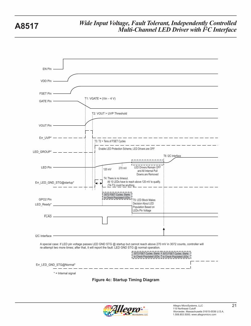
Figure 4c: Startup Timing Diagram
EN Pin
VDD Pin
FSET Pin
T1: VGATE ≈ (Vin – 4 V)
T2: VOUT > UVP Threshold
T3: T2 + Tens of FSET Cycles
T6: I2C Interface
T5: LED Block MakesDecision About LEDPopulation Based onLEDx Pin Voltage
T4: There is no timeout.All 10 LEDs have to reach above 120 mV to qualify.(T4-T3) could be anything.
LED Drivers Remain OFFand All Internal Pull
Downs are Removed
270 mV120 mV
Enable LED Protection Scheme, LED Drivers are OFF
GATE Pin
VOUT Pin
Err_UVP*
LED_GROUP*
LED Pin
Err_LED_GND_STG@startup*
GPO2 Pin
LED_Ready*
FLAG
I2C Interface
* = Internal signal
A special case: if LED pin voltage passes LED GND STG @ startup but cannot reach above 270 mV in 3072 counts, controller willre-attempt two more times; after that, it will report the fault: LED GND STG @ normal operation.
Err_LED_GND_STG@Normal*
3072 FSET Cycles. Startsto Check Populated LEDs.
3072 FSET Cycles. Startsto Check Populated LEDs.
3072 FSET Cycles. Startsto Check Populated LEDs.

Wide Input Voltage, Fault Tolerant, Independently Controlled Multi-Channel LED Driver with I2C InterfaceA8517
22Allegro MicroSystems, LLC115 Northeast CutoffWorcester, Massachusetts 01615-0036 U.S.A.1.508.853.5000; www.allegromicro.com
Output Current and VoltageFor optimal efficiency, the output of the boost stage is dynami-cally adjusted to the minimum voltage required for all active LED strings. This is expressed by the following equation:
VOUT = MAX( VLED1 , VLED2 , … VLED10 )
+ VREG + VHYST (3)
where
VLEDx is the voltage drop across an LED string (only the enabled LED strings are considered),
VREG is the regulation voltage of the LED current sink (0.85 V (typ)), and
VHYST is the hysteresis control voltage at the output (typically 0.25 V).
The boost output voltage is protected by the OVP threshold, which can be programmed up to 39 V. This is sufficient for driv-ing up to 10 white LEDs in series.
The current through each LED string can be programmed through I2C registers to between 1 and 64 mA, in 1 mA steps.
Boost Frequency DitheringThe Boost Dithering function allows the user to randomize the main switching frequency within a certain frequency range. By shifting the main switching frequency of the regulator in a pseudo-random fashion around the main switching frequency, the overall system noise magnitude can be greatly reduced. Note that the frequency dithering function is not available when an external synchronization signal is used at the FSET/SYNC pin.
This spread spectrum functionality is achieved by a program-mable register (0x05[BD1:BD0]. A non-zero number enables the boost dithering and sets the modulation index of 5%, 10%, or 15% of fSW. For example, if 10 % dithering is selected, then the switching frequency will jump between a low of 1.8 MHz and a high of 2.2 MHz, as governed by the pseudo-random pattern.
Every two switching cycles, the switching frequency may ran-domly jump between low and high levels. The random pattern repeats itself after 92 switching cycles. This is illustrated by the timing diagram in Figure 5.
Figure 5: A8517 Dithering Scheme at 2 MHz ±10% (frequency jumps between 1.8 MHz and 2.2 MHz, as governed by a 46-bit pseudorandom pattern)
92 Switching Cycles per Pattern Repeat
Time
Freq
uenc
y (M
Hz)
2.2
1.8
0

Wide Input Voltage, Fault Tolerant, Independently Controlled Multi-Channel LED Driver with I2C InterfaceA8517
23Allegro MicroSystems, LLC115 Northeast CutoffWorcester, Massachusetts 01615-0036 U.S.A.1.508.853.5000; www.allegromicro.com
Polyphase GroupingDuring PWM operation, by default each of the ten LED chan-nels starts at a separate time slot, or phase, (Figure 6, top panel) and with a specified on-time setting. If required, two or more adjacent LED channels can be grouped by programming to turn on and off simultaneously (Figure 6, bottom panel). By tying the corresponding pins together on the PCB, it is possible to combine several channels to drive higher-current LED strings (see Typical Application schematics).
Each LED channel has an LED channel enable bit (0x00 to 0x01) and an LED PWM on-time setting register (0x10 to 0x23). In normal PWM operation, any enabled LED channel is turned on starting at its own time slot, and remains on for the duration con-trolled by its own PWM on-time register. By staggering the time
slots for LED channels, the input ripple current is reduced during PWM operation.
If necessary, such as when more than 1 channel is required to drive an LED string at current higher than 60 mA, the user can group two or more adjacent LED channels together, so that they turn on/off simultaneously. Grouping is done by setting the cor-responding bits in the Polyphase Grouping registers (0x08 and 0x09).
A grouped LED channel starts in the same time slot as the lower-numbered channel, and inherits the PWM Dimming On-Time of that lower-numbered channel (the original time slot of the grouped channel is not used). If more than one adjacent channels are grouped, the entire group starts at the time slot of the lowest-numbered channel in the group, and inherits that on-time setting.
Figure 6: Polyphase Operation
PWM Period
Period /10
Pha
se 1
Pha
se 1
Pha
se 2
Pha
se 3
Pha
se 4
Pha
se 5
Pha
se 6
Pha
se 7
Pha
se 8
Pha
se 9
Pha
se 1
0
Pha
se 1
Pha
se 1
Pha
se 2
Pha
se 3
Pha
se 4
Pha
se 5
Pha
se 6
Pha
se 7
Pha
se 8
Pha
se 9
Pha
se 1
0
Period /10
Polyphase PWM Operation without Grouping – Each LED channel turns-on at a separate, sequential, periodic time slot. The LED on-times are individually programmable, so any individual phase can overlap later time slots.The LED current for each channel is individually programmed.
PWM Period
LED Current
Polyphase PWM Operation with Grouping – The starting time slot and the PWM on-time for each group is determined by the time slot and the on-time of the lowest-numbered channel within that group, so all LED channels in the same group turn-on and turn-off together. Each time slot is sequential and periodic, and unused time slots are maintained. Any individual phase can overlap later time slots. The LED current for each channel is individually programmed, regardless of grouping.
LED Current
ILED1
ILED1
ILED1
ILED1
ILED3
ILED3
ILED4
ILED4
ILED5
ILED5
ILED6
ILED6
ILED7
ILED7
ILED8
ILED8
ILED9
ILED9
ILED10
ILED10
ILED2
ILED2
ILED2
t
t

Wide Input Voltage, Fault Tolerant, Independently Controlled Multi-Channel LED Driver with I2C InterfaceA8517
24Allegro MicroSystems, LLC115 Northeast CutoffWorcester, Massachusetts 01615-0036 U.S.A.1.508.853.5000; www.allegromicro.com
For example, in Figure 6, LED1 and LED2 are grouped together, so they start at PWM slot 1 and follow the on-time of LED1. Similarly, LED3, LED4, and LED5 are grouped together, so they start at PWM slot 3 and follow the on-time of LED3.
If the first LED channel in a polyphase group is disabled through the LED enable register, then all the LEDs in this group are disabled. If any other LED channels in a group are disabled, all of the other LED channels in the group remain enabled, with the PWM on-time of the first LED channel in the group.
Boost Output Voltage RegulationOutput from the boost stage is adaptively adjusted, based on the voltage required by all the enabled LED strings. This ensures minimum power loss at the LED current sinks, and reduces input power consumption.
During operation, the LED string with the highest voltage drop is the dominant string, and it is used to determine the boost output voltage regulation. Because each LED string can be individually enabled/disabled dynamically, which string is dominant can shift at different times.
As an example, assume LED channels 1, 3, and 5 are currently enabled. Further assume that voltage drops across the LED strings are 21 V, 23 V, and 25 V respectively. The boost output voltage will be regulated to the highest LED string voltage (25 V) plus the regulation voltage required by the LED current sink (0.85 V typical):
Table 1: LED String VoltagesLED Channel # LED String
Voltage Drop (V)
Boost Output Voltage
(V)
LEDx Pin Volt-age(V)
1 2125.85 +
Hysteresis
4.85 min
3 23 2.85 min
5 25 (dominant) 0.85 min
For LED strings 1 and 3, the extra voltage is absorbed by their current sinks. When the LED string voltages are poorly balanced (as in this example), excessive power loss can build up at the current sinks. Consider adding ballast resistors to the LED strings with lower voltage drops, so that less heat is dissipated by the IC.
Output HysteresisThe A8517 superposes a minimum output hysteresis of 0.25 V on top of the LED regulation voltage. The OVP pin provides output voltage feedback during hysteresis control mode. An example of
output voltage is show in Figure 7.
When the dominant LED is on, boost stage starts switching to keep the corresponding LEDx pin voltage regulated to VREG . After the dominant LED is turned off, the switching continues until boost output reaches VTH(+). The output is then regulated between VTH(–) and VTH(+) through hysteresis control, before the next time dominant LED is on again.
Soft Start TimingThe soft-start function performs the following sequence of operation:
1. At startup, the boost stage initially switches at the minimum SW on-time continuously. This allows output voltage to build-up, even at the minimum PWM duty cycle.
2. The switch on-time increases as the COMP pin voltage starts to rise (the COMP voltage controls the boost stage switching duty cycle, which in turn controls the boost output voltage).
3. Soft start ramp duration is 100 ms, which allows the LED to cycle 10 times at a 100 Hz PWM frequency.
4. Soft start can finish earlier, either due to the LED current reaching regulation, or because output voltage reaches 90% of OVP.
5. To prevent output voltage from reaching 90% of OVP prema-turely (while the COMP voltage is still too low), the design should ensure there is sufficient output capacitance, such that it takes longer to build up VOUT at the minimum SW on-time.
6. During soft start, the PWM on-time needs to be at least 1.5 µs to guarantee reliable detection once LED current reached regulation. If the startup on-time is set lower (at 1 µs, for example), soft start may be terminated later when output reached 90% OVP level.
It is important not to set OVP level too much higher than the normal operating voltage of LED strings. In particular, make sure that:
VLED + VREG < VOVP < VLED + VREG + VSD where VLED is the worst-case/highest voltage drop across LED strings. VREG is the LED pin regulation volatge (around 1 V). VSD is the LED string short-detect threshold (programmable between 5 and 12 V).
For Boost configuration with 7 to 10 LEDs in series, OVP is typi-cally set at ~5 V above the worst-case LED string voltage. For SEPIC configuration with lower number of LEDs in series, OVP may be set closer to the LED voltage.

Wide Input Voltage, Fault Tolerant, Independently Controlled Multi-Channel LED Driver with I2C InterfaceA8517
25Allegro MicroSystems, LLC115 Northeast CutoffWorcester, Massachusetts 01615-0036 U.S.A.1.508.853.5000; www.allegromicro.com
Input Disconnect SwitchThe A8517 has a gate driver for an external PMOS that can be used to provide an input disconnect protection function. During normal startup, the PMOS is turned on gradually to avoid large inrush current. In the event there is a direct short at the boost stage (either SW or VOUT shorted to GND), high input current will cause the PMOS to turn off.
The input disconnect current threshold is calculated by:
IINMAX = VINS(TH) / RINS (4)where VINS(TH) = 105 mV (typ).
Under normal operation, the input current is protected by the cycle-by-cycle boost switch current limit. Only in case of a direct short at boost output or SW pin will the input disconnect switch be activated. Therefore the input disconnect current threshold is typically set slightly higher than the switch current limit. For example, choose RINS = 0.02 Ω to set IINMAX = 5.25 A approxi-mately.
During normal power-up sequence, as soon as EN goes high, the
GATE pin will start to be pulled low by a 115 µA (typ) current. How quickly the external PMOS turns on depends on the gate capacitance, CGS, of the PMOS. If the gate capacitance is very low, the inrush current may still exceed 5 A momentarily and trip the input disconnect protection. In this case, an external CGS may be added to slow down the PMOS turn-on. A typical value of 10 nF should be sufficient in most cases.
When selecting the external PMOS, check for the following parameters:
• Drain-source breakdown voltage: BVDSS > –50 V
• Gate threshold voltage: ensure it is fully enhanced at VGS = –4 V, and cut-off at –1 V
• RDS(on): ensure the on-resistance is rated at VGS = –4.5 V or similar, not at –10 V; derate it for higher temperatures
The PMOS gate voltage is clamped by the A8517 such that VGS = VIN – VGATE ≤ 8 V. This is to prevent the gate-source of external PMOS from breaking down due to higher input voltage. In case of very low input voltage, however, VGS is limited by VIN. There-fore it is important to select a PMOS with a lower gate threshold voltage.
Test conditions:LED1 and LED2 = 8 series (dominant LED string), LED4, LED5, LED6 = 7 seriesAll other channels disabled 60 mA each enabled channelLED VREG = 0.85 V VIN = 12 V VOUT hysteresis = 0.25 V
Scope traces:C1 (Yellow) = VGPO1 PWM period (5 V/div) C3 (Blue) = VOUT (1 V/div, offset = 24 V) C4 (Green) = Total ILEDx (50 mA/div) Time scale = 500 µs/div
A8517 evaluation PCB:L1 = 10 µH, COUT5 = 68 µF / 50 V polymer electrolytic, COUT4 = 2.2 µF / 50 V 1206 ceramic, RZ = 10 kΩ, CZ = 5.6 nF, CP = 120 pF
Figure 7: Output Hysteresis Waveform, LED1 and LED2 are the Dominant String
PWM Period
VOUT controlled by dominant LED string
LED1 and LED2 on(dominant)
LED4, LED5, and LED6 on
VOUT under hysteresis control

Wide Input Voltage, Fault Tolerant, Independently Controlled Multi-Channel LED Driver with I2C InterfaceA8517
26Allegro MicroSystems, LLC115 Northeast CutoffWorcester, Massachusetts 01615-0036 U.S.A.1.508.853.5000; www.allegromicro.com
System Failure Detection and ProtectionThe A8517 is designed to detect and protect against a multitude of system-level failures. Some of those possible faults are illus-trated in Figure 8 and the A8517 is described in Table 2.
Table 2: System Failure ModeFailure Mode Symptom Protected? A8517 Response
Inductor open Output undervoltage fault detected at startup Yes Will not proceed with startup
Inductor shorted Excessive current through SW pin during switching, secondary OCP tripped Yes Shuts down and will not retry
Diode open Excessive voltage detected at SW pin, secondary OVP tripped Yes Shuts down and will not retry
Diode shorted Excessive current through SW pin during switching Yes Shuts down and will not retry
Output shorted to GND Input overcurrent protection tripped at startup Yes Shuts off input power via input disconnect switch
LED string open or LEDx pin open
IC unable to detect LED current, output ramps up and trips OVP Yes Disable offending LED string, other strings
continue to operate
LEDs shorted within one string Excessive voltage drop at LEDx pin Yes Disable offending LED string, other strings
continue to operate
LEDx pin to GND short at startup
Detected LED pin to GND short during startup error check Yes Will not proceed until fault is removed
LEDx pin to GND short during operation
IC unable to detect LED current, output ramps up and trips OVP Yes Shuts down and rechecks for pin to GND short
before restart
FSET pin to GND short or FSET pin open IC unable to start switching Yes Will not restart until fault is removed
External synchronization signal disconnected Unable to detect logic signal at FSET pin Yes Falls back to switching frequency determined
by RFSET
COUT
OVP
Q1 CQ1
L1
INS
LED1
LED2
LED10
RFSET
GATE
GND
VIN
SWPGND
FSET/SYNC
CIN
A8517
D1 VOUT
ExternalSynchronization
RSENSE
VIN
Inductor open/short
Diode open/short
Output to GND short
LED shortwithin string
LED stringopen
LEDx pin to GND short
FSET pin to GND short
Synchronization signal loss
Figure 8: Examples of System Fault Modes
Wide Input Voltage, Fault Tolerant, Independently Controlled Multi-Channel LED Driver with I2C InterfaceA8517
27Allegro MicroSystems, LLC115 Northeast CutoffWorcester, Massachusetts 01615-0036 U.S.A.1.508.853.5000; www.allegromicro.com
Fault HandlingThe A8517 can detect and monitor 12 different fault modes internally. Some can be programmed for latching (flag set, system controller action required) or for auto restart after flag set and condition cleared. Faults are listed in Table 3.
In the event of a fault, registers 0x38 and 0x39 hold the fault status to allow the master to read what type of fault (such as OCP, OVP, open LED, and so forth) has been detected.
INTERNAL STATE MONITORINGThere are two general-purpose output pins, GPO1 and GPO2, that can be programmed to monitor selected internal status bits directly. This allows those pins to be used as special IRQ (inter-rupt request) lines for the system. The system can also moni-tor non-critical fault occurrences (such as temperature warning or SW current limit) while the IC continues to run. GPO1 and GPO2 are open-drain outputs, and an external pull-up resistor is required at each pin to set the logic-high level required.
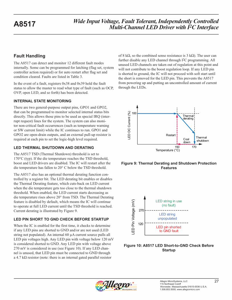
LED THERMAL SHUTDOWN AND DERATINGThe A8517 TSD (Thermal Shutdown) threshold is set to 170°C (typ). If the die temperature reaches the TSD threshold, boost and LED drivers are disabled. The IC will restart after the die temperature has fallen to 20° C below the TSD threshold.
The A8517 also has an optional thermal derating function con-trolled by a register bit. The LED derating bit enables or disables the Thermal Derating feature, which cuts-back on LED current when the die temperature gets too close to the thermal shutdown threshold. When enabled, the LED current starts decreasing as die temperature rises above 20° from TSD. The Thermal Derating feature is disabled by default, which means the IC will continue to operate at full LED current until the TSD threshold is reached. Current derating is illustrated by Figure 9.
LED PIN SHORT TO GND CHECK BEFORE STARTUPWhen the IC is enabled for the first time, it checks to determine if any LED pins are shorted to GND and/or are not used (LED string not populated). An internal 60 µA current source pulls all LED pin voltages high. Any LED pin with voltage below 120 mV is considered shorted to GND. Any LED pin with voltage above 270 mV is considered in use (see Figure 10). If any LED chan-nel is unused, that LED pin must be connected to GND through a 4.7 kΩ resistor (note: there is an internal gated parallel resistor
of 8 kΩ, so the combined sense resistance is 3 kΩ). The user can further disable any LED channel through I2C programming. All unused LED channels are taken out of regulation at this point and will not contribute to the boost regulation loop. If any LED pin is shorted to ground, the IC will not proceed with soft start until the short is removed for the LED pin. This prevents the A8517 from powering up and putting an uncontrolled amount of current through the LEDs.
Figure 10: A8517 LED Short-to-GND Check Before Startup
LED
Pin
Vol
tage
(mV
)
270
LED pin shorted to GND fault
120
LED string in use (no fault)
LED string unpopulated
Figure 9: Thermal Derating and Shutdown Protection Features
LED
DC
Cur
rent
(%)
Temperature (°C)150 170
100
Thermal derating
Thermal shutdownCool
down
Restart

Wide Input Voltage, Fault Tolerant, Independently Controlled Multi-Channel LED Driver with I2C InterfaceA8517
28Allegro MicroSystems, LLC115 Northeast CutoffWorcester, Massachusetts 01615-0036 U.S.A.1.508.853.5000; www.allegromicro.com
LED PIN OPEN/SHORT FAULT DURING NORMAL OP-ERATION
During startup and normal operation, all enabled LED channels are supposed to ramp up in current until each channel regula-tion target is reached. If any channel is below regulation, it will request the boost output voltage to rise, so the higher voltage can help more current to flow through its LED string. But in the event that an LED pin is either open or shorted to ground, there can be no current flowing through its LED driver. The boost voltage will continue to rise until the OVP fault is tripped.
This function is used in conjunction with general fault 8 (overvoltage protection), so it can be monitored by the I2C mas-ter. When this bit is set to 0, the corresponding LED channel is within regulation and operating correctly (or the LED channel has been previously disabled). When the OVP fault is tripped the bit is set to 1.
When the OVP fault is tripped, any enabled LED channel that is not in regulation is tested for ground-short again:
• If an unregulated channel is shorted to ground, the boost stage is shutdown completely and will not attempt auto-restart. This
is to prevent uncontrolled current from flowing through the LED string. Fault flag is set to signal an LED to GND short fault (#11). The corresponding bit in the LED Pin Shorted to GND status register is set. The user can then read this register to determine which LED channel is shorted.
• If an unregulated channel is not shorted to ground, the IC will remove the offending channel from regulation, and resume normal operation for other channels. The F ¯ L A G pin (which was previously set to signal an OVP fault) is then cleared. The corresponding bit in the Latched Status LEDs in Regulation registers (0x3A and 0x3B) is set. The user can then read this register to determine which LED channel is open.
Note:If the OVP level is programmed too low in the OVP Threshold register for the LED string with highest forward voltage, the LED driver may not be able to reach regulation during startup. In this case, the IC will treat the LED pin as open. The offending LED pin is removed from regulation and the rest of the
LED channels will resume normal operation.

Wide Input Voltage, Fault Tolerant, Independently Controlled Multi-Channel LED Driver with I2C InterfaceA8517
29Allegro MicroSystems, LLC115 Northeast CutoffWorcester, Massachusetts 01615-0036 U.S.A.1.508.853.5000; www.allegromicro.com
Number andName
Default Action Programmable? Input Disconnect Switch Boost Switch LED Current F L A G Set
on Fault?
Fault 1Input Overcurrent
Latched No Off Off Off Yes
This fault is set when an input overcurrent has been detected (VIN – VINS > 100 mV). The input disconnect switch is disabled, as well as the boost stage and LED drivers. The fault flag is latched at low. To reenable the part, the EN pin must be cycled.
Fault 2 Output Undervoltage
Auto Restart Yes On Off Off Yes
The IC monitors the output voltage on the OVP pin. If the voltage level drops below output undervoltage threshold, VUVP (such as in case of output shorted to GND), the fault will be registered. The boost SW and LED drivers are shut down.
Fault 3Temperature Warning
Auto Restart Yes On On Reduced No
This is a warning that the IC is approaching thermal shutdown. Typically this fault is asserted at 20°C below TSD, and LED current is reduced. As soon as the IC cools down, the fault bit will reset.
Fault 4Overtemperature Protection
Auto Restart No On Off Off Yes
Fault occurs when the die temperature exceeds the TSD (thermal shutdown) threshold, typically 170°C.
Fault 5FSET Short Protection
Auto Restart Yes On Off Off Yes
Fault occurs when the FSET/SYNC current exceeds approximately 180 µA (≈150% of maximum current). The boost will stop switching, and the IC will disable the LED sinks until the fault is removed.
Fault 6SW Primary Current Limit
Auto Restart No On Truncated On No
The device monitors its switch current on a cycle-by-cycle basis, and shuts the switch off for the existing cycle if the current exceeds ISW(LIM). Normal switching continues in the next cycle. This fault does not shut down the IC.
Fault 7SW Secondary Current Limit
Latched No Off Off Off Yes
When the current through the boost SW pin exceeds secondary current limit (ISWLIM(sec) ), the part will immediately shut down the input disconnect switch, LED drivers, and boost. To restart the part, either cycle the power or toggle the EN pin.
Fault 8Overvoltage Protection
Auto Restart Yes On Off On Yes
Fault occurs when the OVP pin exceeds the VOVP(th) threshold.Case 1. All enabled LED strings are in regulation. The IC will immediately stop boost switching. LED current sinks remain active to drain the output voltage. After the output voltage falls below approximately 94% of the OVP threshold, the IC will resume switching to regulate the output voltage.Case 2. One (or more) enabled LED string is not in regulation. See Fault 11.
Fault 9Open Diode Protection
Latched No Off Off Off Yes
Secondary overvoltage protection at the SW pin is used for open diode detection. When diode D1 opens up, the SW pin voltage will increase until VOVP(sec) is reached. The input disconnect switch is disabled, as well as the boost stage and LED drivers. The F L A G pin is pulled low only while the overvoltage condition exists. To restart the part, either cycle the power or toggle the EN pin.
Fault 10LED Pin Shorted to GND During Startup
Auto Restart Yes On Off Off Yes
The system at power-up checks if an LED pin is shorted to GND (see the LED Pin Short to GND Check before Startup section for details). If any pin is shorted, the system will not power up and the fault flag will be set.
Continued on the next page…
Table 3: Internal Fault Modes

Wide Input Voltage, Fault Tolerant, Independently Controlled Multi-Channel LED Driver with I2C InterfaceA8517
30Allegro MicroSystems, LLC115 Northeast CutoffWorcester, Massachusetts 01615-0036 U.S.A.1.508.853.5000; www.allegromicro.com
Number andName
Default Action Programmable? Input Disconnect Switch Boost Switch LED Current F L A G Set
on Fault?
Fault 11LED Pin Shorted to GND During Normal Operation
Latched Yes On Off Off Yes
This fault occurs when the LED pin is not in regulation and the output reaches OVP. At this time, the system removes LED from the regulation loop, allowing the high output voltage to fall. After this LED is disabled, the IC will determine whether the LED pin is shorted to GND or open (see the LED Pin Open/Short Fault during Normal Operation section for details). If the LED pin is open, the IC will continue to operate with the offending LED turned off. If LED pin is shorted to GND, the IC will shut down and latch off. To restart the part, either cycle the power or toggle the EN pin.
Fault 12LED String Short Detect
Auto Restart Yes On On On* Yes
This fault is set if any LED pin voltage goes above its LED Short-Detect Threshold (set by corresponding programmable register bits). The offending LED driver is disabled immediately. Other LED strings will continue to work as normal. At the next PWM cycle, the offending LED driver is checked again and may resume operation if the fault has been removed (unless the Auto-restart bit is turned off).
*Only the offending LED driver is turned off. All other enabled LED drivers continue to work as normal.
Table 3: Internal Fault Modes (continued)
Wide Input Voltage, Fault Tolerant, Independently Controlled Multi-Channel LED Driver with I2C InterfaceA8517
31Allegro MicroSystems, LLC115 Northeast CutoffWorcester, Massachusetts 01615-0036 U.S.A.1.508.853.5000; www.allegromicro.com
COUT
CVDD
OVP
Q1
L1
INS
VDD LED1 to 4
LED6 to 9
LED5
2 strings of 10 LEDs in series240 mA maximum per stringVOUT = 34 V nominal
CZ
RZ
LED10
RFSET
RADDR
CP
GATE
EN
FLAG
VIN (6 to 18 V)
SW
COMP
PGND
AGND
FSET/SYNC
CIN CQ1
VC
SDA
SCL
ADDR
A8517
D1 VOUT (39 V maximum)
ExternalSync
RSENSE
VIN
GPO1 GPO2
I2C Interface
PAD
VC
Status /Interrupt
GND
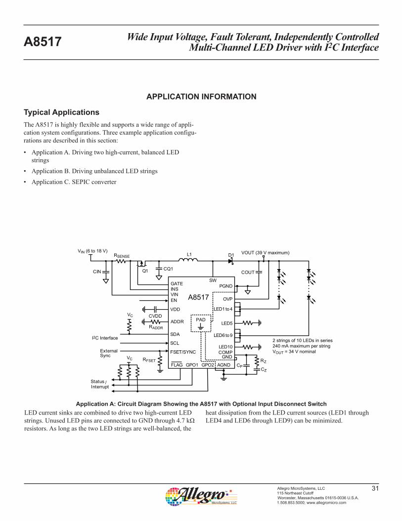
APPLICATION INFORMATION
Typical ApplicationsThe A8517 is highly flexible and supports a wide range of appli-cation system configurations. Three example application configu-rations are described in this section:
• Application A. Driving two high-current, balanced LED strings
• Application B. Driving unbalanced LED strings
• Application C. SEPIC converter
LED current sinks are combined to drive two high-current LED strings. Unused LED pins are connected to GND through 4.7 kΩ resistors. As long as the two LED strings are well-balanced, the
heat dissipation from the LED current sources (LED1 through LED4 and LED6 through LED9) can be minimized.
Application A: Circuit Diagram Showing the A8517 with Optional Input Disconnect Switch
Wide Input Voltage, Fault Tolerant, Independently Controlled Multi-Channel LED Driver with I2C InterfaceA8517
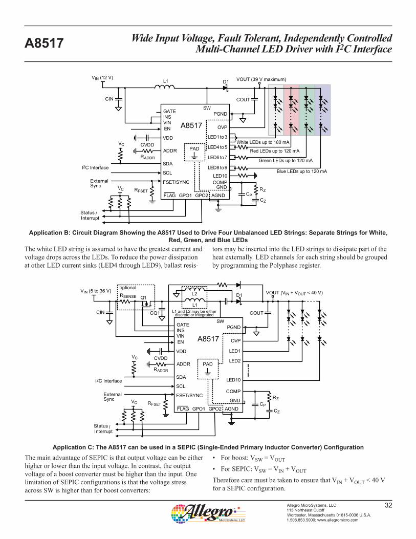
32Allegro MicroSystems, LLC115 Northeast CutoffWorcester, Massachusetts 01615-0036 U.S.A.1.508.853.5000; www.allegromicro.com
COUT
CVDD
OVP
L1
INS
VDD LED1 to 3
LED4 to 5White LEDs up to 180 mA
Red LEDs up to 120 mA
Green LEDs up to 120 mA
Blue LEDs up to 120 mA
RFSET
RADDR
GATE
EN
FLAG
VIN (12 V)
SW
COMP
PGND
AGND
FSET/SYNC
CIN
VC
SDA
SCL
ADDR
A8517
D1 VOUT (39 V maximum)
ExternalSync
LED10
VIN
GPO1 GPO2
I2C Interface
PAD
VC
Status /Interrupt
LED6 to 7
LED8 to 9
GNDCP
CZ
RZ
COUT
CVDD
OVP
Q1 L1
INS
VDD LED1
LED2PAD
LED10
RFSET
RADDR
CZ
RZ
GATE
EN
FLAG
VIN (5 to 36 V)
SW
COMP
PGND
AGND
FSET/SYNC
CIN CQ1
L2
VC
VC
SDA
SCL
ADDR
A8517
D1
ExternalSync
RSENSE
VIN
GPO1 GPO2
Status /Interrupt
I2C Interface
VOUT (VIN + VOUT < 40 V)optional
L1 and L2 may be eitherdiscrete or integrated
GNDCP
The white LED string is assumed to have the greatest current and voltage drops across the LEDs. To reduce the power dissipation at other LED current sinks (LED4 through LED9), ballast resis-
tors may be inserted into the LED strings to dissipate part of the heat externally. LED channels for each string should be grouped by programming the Polyphase register.
The main advantage of SEPIC is that output voltage can be either higher or lower than the input voltage. In contrast, the output voltage of a boost converter must be higher than the input. One limitation of SEPIC configurations is that the voltage stress across SW is higher than for boost converters:
• For boost: VSW = VOUT
• For SEPIC: VSW = VIN + VOUT
Therefore care must be taken to ensure that VIN + VOUT < 40 V for a SEPIC configuration.
Application B: Circuit Diagram Showing the A8517 Used to Drive Four Unbalanced LED Strings: Separate Strings for White, Red, Green, and Blue LEDs
Application C: The A8517 can be used in a SEPIC (Single-Ended Primary Inductor Converter) Configuration

Wide Input Voltage, Fault Tolerant, Independently Controlled Multi-Channel LED Driver with I2C InterfaceA8517
33Allegro MicroSystems, LLC115 Northeast CutoffWorcester, Massachusetts 01615-0036 U.S.A.1.508.853.5000; www.allegromicro.com
Design ExampleThis section provides a method for selecting component values when designing an application using the A8517. The results are diagrammed in the schematic shown in Figure 11 at the end of this design example.
The following requirements are considered for this design example:
• VIN: 10 to 14 V
• Quantity of LED channels (strings), n: 10
• Quantity of series LEDs per channel, nsl: 7
• LED current per channel, ILED: 60 mA
• LED voltage drop, Vf : 3 V at 60 mA
• Boost diode forward voltage,Vd: 0.4 V
• fSW : 2 MHz
• PWM dimming frequency: 200 Hz at 100% duty cycle
• Polyphase feature is turned on
• At 12 V and 60 mA/channel, the IC case temperature rise is measured to be 40°C. At lower VIN , the IC case and junction temperature rise will increase. Therefore, if proper cooling is not applied, output current derating would be required.
STEP 1: Determining the output voltage. The output voltage is determined by the following equation:
VOUT = nsl × Vf + VLED + 0.45 (V) . (5)The regulated VLED is 0.85 V. The fixed 0.45 V is related to the output-implemented voltage hysteresis control. During PWM dimming on-time, VLED is regulated to 0.85 V. During PWM dimming off-time, the output voltage hysteresis control is 0.45 V. Substituting into equation 5:
VOUT = 7 × 3 (V) + 0.85 (V) + 0.45 (V) = 22.3 V .STEP 2: Determining the OVP threshold limit. This is the maxi-mum voltage based on the LED requirements. The regulation voltage, VLED , of the A8517 is 0.85 V. A constant term, 5 V, is added to give some margin to the design:
VOUT(OVP) = nsl × Vf + VLED + 0.45 (V) + 5 (V) . (6)
Substituting into equation 6:
VOUT(OVP) = 7 × 3 (V) + 0.85 (V) + 0.45 (V) + 5 (V) = 27.3 V .In the OVP Threshold register (0x04), set the OVP threshold to 28 V.
STEP 3: At this point, a quick check should be done to determine if the conversion ratio is acceptable for the selected frequency. First, determine the maximum duty cycle:
DMAX = 1 – tSWOFFTIME(max) × fSW , (7)where tSWOFFTIME(max), 85 ns, is found in the datasheet. Substi-tuting into equation 7:
DMAX = 1 – (0.085 (µs) × 2 (MHz)) = 0.83 .Then the theoretical maximum voltage, VOUTMAX , is calculated as:
VOUTMAX = [VINMIN / (1– DMAX )] – Vd , (8)where Vd is the boost diode forward voltage. Substituting into equation 8:
VOUTMAX = [10 (V) / (1 – 0.83)] – 0.4 (V) = 58.42 V .The theoretical maximum voltage value must be greater than the value VOUT(OVP) . If this is not the case, the switching frequency of the boost converter must be reduced to meet the maximum duty cycle requirements.
STEP 3: Selecting the inductor. The inductor must be chosen such that it can handle the necessary input current. In most applica-tions due to stringent EMI requirements the system must operate in continuous conduction mode (CCM) at least throughout the normal selected input voltage range and nominal output current.
STEP 3a: Determining the maximum operating duty cycle in CCM. The duty cycle is calculated as follows:
DCCM(MAX) = 1 – VINMIN / (VOUT(OVP) + Vd ) , (9)and substituting into equation 9:
DCCM(MAX) = 1 – 10(V) / (28 (V) + 0.4 (V)) = 0.65.STEP 3b: Determining the maximum and minimum input current to the system. The minimum input current will dictate the induc-tor value. The maximum input current will dictate the current rating of the inductor.

Wide Input Voltage, Fault Tolerant, Independently Controlled Multi-Channel LED Driver with I2C InterfaceA8517
34Allegro MicroSystems, LLC115 Northeast CutoffWorcester, Massachusetts 01615-0036 U.S.A.1.508.853.5000; www.allegromicro.com
First, calculate the maximum input current. The input current is output-determined, so:
IOUT = n × ILED , (10)given ILED = 60 mA, substituting into equation 10:
IOUT = 10 × 0.060 (A) = 0.6 (A) .IOUT can be used to calculate the maximum input current:
IINMAX = (VOUT(OVP) × IOUT ) / (VINMIN × η) , (11)where η is the efficiency value, which can be obtained from efficiency curves in this datasheet (at fSW = 2 MHz). It is approxi-mately 80% under these conditions. Substituting into equation 11:
IINMAX = (28 (V) × 0.60 (A) ) / (10 (V) × 0.8) = 2.1 A .Similarly, calculate the minimum input current:
IINMIN = (VOUT × IOUT ) / (VINMAX × η) , (12)where VOUT is determined by equation 5, and η is the efficiency value, which can be obtained from efficiency curves in this datasheet (at fSW = 2 MHz). It is approximately 85% under these conditions. Substituting into equation 12:
IINMIN = (22.3 (V) × 0.60 (A) ) / (14 (V) × 0.85) = 1.12 A .STEP 3c: Determining the inductor value. To ensure that the inductor operates in continuous conduction mode, the value of the inductor must be set such that the 1/2 inductor ripple current is not greater than the average minimum input current:
ΔIL = IINMAX × kripple . (13)A practical starting point is to consider kripple to be 40% of the maximum inductor current. Substituting into equation 13:
ΔIL= 2.1 (A) × 0.4 = 0.84 AThe inductor value can then be calculated as:
L1 = VINMIN / (ΔIL × fSW ) × DCCM(MAX) . (14)where DCCM(MAX) is calculated as in equation 9. Substituting into equation 14:
L1 = 10 (V) / (0.84 (A) × 2 (MHz)) × 0.65 = 3.87 µHDouble-check to make sure that the 1/2 inductor ripple current is less than IINMIN , by applying equations 12 and 13:
IINMIN > (1/2) × ΔIL
1.12 > 0.42 A .For lower ripple current, smaller output capacitor, and higher effi-ciency, we selected the inductor value to be 10 µH.
STEP 3d: This step is used to verify that there is sufficient slope compensation for the chosen inductor.
The ripple current when L = 10 µH is given by:
ΔILused = (VINMIN × DCCM(MAX) ) / (Lused × fSW ) . (15)Substituting into equation 15:
ΔILused = (10 (V) × 0.65) / (10 (µH) × 2.0 (MHz)) = 0.325 A .The minimum required slope compensation is proportional to the switching frequency and it is given by:
S =E(MINREQ)
× ( 1 D )– CCM(MAX)fSW
∆I × (∆s × 10 )Lused
-6
1(16)
where Δs is taken from Riddley’s formula:
Δs = 1 – 0.18/DCCM(MAX) (17)
= 1 – 0.18 / 0.65 = 0.723 .Substituting into equation 16:
S =E(MINREQ)
× ( 1 0.65 )–2.0 (MHz)
0.325 (A) × (0.723 × 10 )-6
= 1.34 A / µs
1
At 2 MHz switching frequency, 2.3A/µs slope compensation is implemented in the A8517 (programmable through the I2C inter-face). If the implemented value is less than the figure calculated using equation 16, then the inductor value must be increased.
STEP 3e: Determining the inductor current rating. The minimum inductor current rating can be calculated as follows:
ILMIN = IINMAX + 1/2 × ΔIL (18)
= 2.1 (A) + 0.325 (A) / 2
= 2.26 A
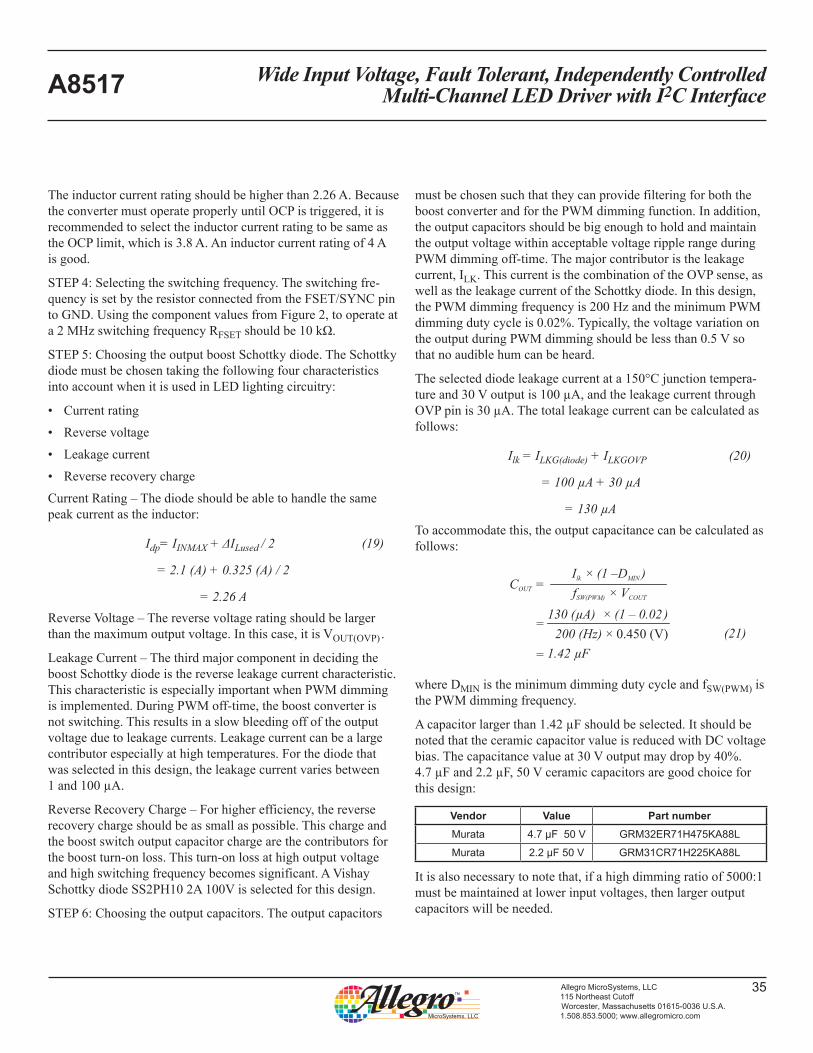
Wide Input Voltage, Fault Tolerant, Independently Controlled Multi-Channel LED Driver with I2C InterfaceA8517
35Allegro MicroSystems, LLC115 Northeast CutoffWorcester, Massachusetts 01615-0036 U.S.A.1.508.853.5000; www.allegromicro.com
The inductor current rating should be higher than 2.26 A. Because the converter must operate properly until OCP is triggered, it is recommended to select the inductor current rating to be same as the OCP limit, which is 3.8 A. An inductor current rating of 4 A is good.
STEP 4: Selecting the switching frequency. The switching fre-quency is set by the resistor connected from the FSET/SYNC pin to GND. Using the component values from Figure 2, to operate at a 2 MHz switching frequency RFSET should be 10 kΩ.
STEP 5: Choosing the output boost Schottky diode. The Schottky diode must be chosen taking the following four characteristics into account when it is used in LED lighting circuitry:
• Current rating
• Reverse voltage
• Leakage current
• Reverse recovery charge
Current Rating – The diode should be able to handle the same peak current as the inductor:
Idp= IINMAX + ΔILused / 2 (19)
= 2.1 (A) + 0.325 (A) / 2
= 2.26 AReverse Voltage – The reverse voltage rating should be larger than the maximum output voltage. In this case, it is VOUT(OVP) .
Leakage Current – The third major component in deciding the boost Schottky diode is the reverse leakage current characteristic. This characteristic is especially important when PWM dimming is implemented. During PWM off-time, the boost converter is not switching. This results in a slow bleeding off of the output voltage due to leakage currents. Leakage current can be a large contributor especially at high temperatures. For the diode that was selected in this design, the leakage current varies between 1 and 100 µA.
Reverse Recovery Charge – For higher efficiency, the reverse recovery charge should be as small as possible. This charge and the boost switch output capacitor charge are the contributors for the boost turn-on loss. This turn-on loss at high output voltage and high switching frequency becomes significant. A Vishay Schottky diode SS2PH10 2A 100V is selected for this design.
STEP 6: Choosing the output capacitors. The output capacitors
must be chosen such that they can provide filtering for both the boost converter and for the PWM dimming function. In addition, the output capacitors should be big enough to hold and maintain the output voltage within acceptable voltage ripple range during PWM dimming off-time. The major contributor is the leakage current, ILK. This current is the combination of the OVP sense, as well as the leakage current of the Schottky diode. In this design, the PWM dimming frequency is 200 Hz and the minimum PWM dimming duty cycle is 0.02%. Typically, the voltage variation on the output during PWM dimming should be less than 0.5 V so that no audible hum can be heard.
The selected diode leakage current at a 150°C junction tempera-ture and 30 V output is 100 µA, and the leakage current through OVP pin is 30 µA. The total leakage current can be calculated as follows:
Ilk = ILKG(diode) + ILKGOVP (20)
= 100 µA + 30 µA
= 130 µATo accommodate this, the output capacitance can be calculated as follows:
C =OUTf × VSW(PWM) COUT
I × (1 –D )lk MIN
× 0.450 (V)200 (Hz)
1.42 µF
130 (µA) × (1 – 0.02 )=
=
(21)
where DMIN is the minimum dimming duty cycle and fSW(PWM) is the PWM dimming frequency.
A capacitor larger than 1.42 µF should be selected. It should be noted that the ceramic capacitor value is reduced with DC voltage bias. The capacitance value at 30 V output may drop by 40%. 4.7 µF and 2.2 µF, 50 V ceramic capacitors are good choice for this design:
Vendor Value Part numberMurata 4.7 µF 50 V GRM32ER71H475KA88L
Murata 2.2 µF 50 V GRM31CR71H225KA88L
It is also necessary to note that, if a high dimming ratio of 5000:1 must be maintained at lower input voltages, then larger output capacitors will be needed.

Wide Input Voltage, Fault Tolerant, Independently Controlled Multi-Channel LED Driver with I2C InterfaceA8517
36Allegro MicroSystems, LLC115 Northeast CutoffWorcester, Massachusetts 01615-0036 U.S.A.1.508.853.5000; www.allegromicro.com
The rms current through the capacitor is given by:
D +CCM(MAX)
1 – DCCM(MAX)
× 12IINMAX
ΔILused
C = I ×OUTrms OUT
0.65+
1 – 0.65
× 122.1 (A)
0.325 (A)
= 0.6 (A) ×
= 0.826 A
(22)
The output capacitor must have a current rating of at least 0.826 A. The capacitors selected in this design have a combined current rating of 3 A.
STEP 7: Selecting the input capacitor. The input capacitor must be selected such that it provides a good filtering of the input volt-age waveform. A good rule of thumb is to set the input voltage ripple, ΔVIN , to be 1% of the minimum input voltage. To accom-modate this, the input capacitance can be calculated as follows:
C =IN 8 × f × ∆VSW IN
∆ILused
8 × 2 (MHz) × 0.1 (V)
= 0.203 µF
0.325 (A)= (23)
The rms current through the capacitor is given by:
(1 – D ) × 12CCM(MAX)
IINMAX
ΔILused
C = I ×INrms OUT
(1 – 0.65) × 12
2.1 (A)
0.325 (A)
= 0.6 (A) ×
= 0.076 A
(24)
4.7 µF and 2.2 µF, 50 V ceramic capacitors are good choice for this design, shown in the following table:
Vendor Value Part numberMurata 4.7 µF 50 V GRM32ER71H475KA88L
Murata 2.2 µF 50 V GRM31CR71H225KA88L
If long wires are used for the input, it is necessary to use a much larger input capacitor. A larger input capacitor is also required to have stable input voltage during line transients.
STEP 8: Choosing the input disconnect switch components. Choose a P-channel MOSFET disconnect switch with current rat-ing the same or higher than the IC trip threshold current limit, Set the limit to be 5 A.
The IC trip current limit, ILIM , can be set by the input current sense resistor. When the IC detects VINSTRIP , 105 mV (typ), across the input current sense resistor, it turns off the disconnect switch. The sense resistor value can be calculated as follows:
RSENSE = VINSTRIP / ILIM (25)
= 0.105 (V) / 5 (A)
= 0.021 ΩA 18 mΩ / 0.5 W, 1206 resistor is selected. Therefore, the actual current limit is calculated by rearranging equation 25:
ILIM = 0.105 V / 0.018 Ω = 5.8 A
The AO4421 6.2 A / 60 V P-channel MOSFET is selected.
STEP 9: Selecting the ADDR pin resistor value. Use a 0 Ω resis-tor address 100 0000.
STEP 10: Selecting the SDA pin pull-up resistor. Use a 2 kΩ resistor to VCC.
STEP 11: Selecting the F ¯ L A G , GPO1, and GPO2 pull-up resis-tors. For each of these output pins, use a 10 kΩ resistor to VCC.
STEP 12: Selecting the output LEDs. High power white 3000 K 85 CRI Duris E5 (LCW JDSHEC-EUFQ-5R8T-1) LEDs were selected.
STEP 13: Selecting CQ1 , placed from the drain of Q1 to GND. The purpose of this capacitor is to absorb the negative spike gen-erated by L1 when the input disconnect switch is turned off. Use a small value such as 1 µF / 50 V ceramic. A large value may trip OCP during startup or a fast VIN transient.
STEP 14: See appendix A for a detailed description of how to calculate RZ, CZ, and CP. Using L1 = 10 µH, COUT = (4.7 µF + 2.2 µF ), and fC = 30 kHz, the calculation results for RZ , CZ , and CP are: RZ = 240 Ω, CZ = 220 nF, and CP = 100 pF.
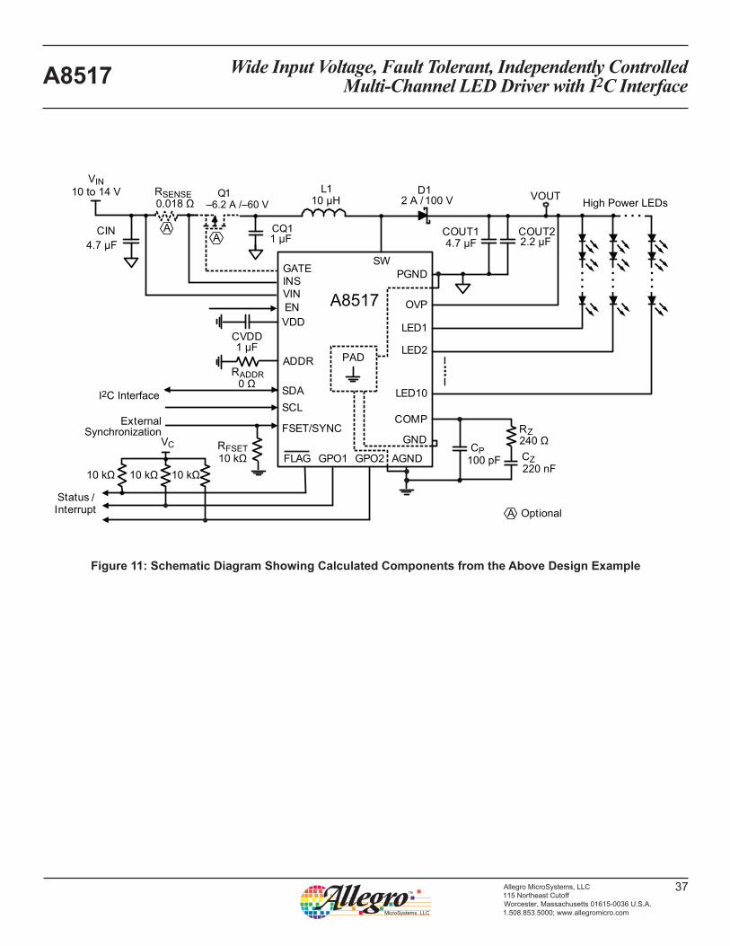
Wide Input Voltage, Fault Tolerant, Independently Controlled Multi-Channel LED Driver with I2C InterfaceA8517
37Allegro MicroSystems, LLC115 Northeast CutoffWorcester, Massachusetts 01615-0036 U.S.A.1.508.853.5000; www.allegromicro.com
Figure 11: Schematic Diagram Showing Calculated Components from the Above Design Example
COUT14.7 µF
COUT22.2 µF4.7 µF
CVDD
OVP
Q1
CQ1
–6.2 A /–60 VL1
INS
VDD LED1
LED2PAD
LED10
RFSET
RADDR
CZ
RZ
GATE
EN
FLAG
VIN 10 to 14 V
SW
COMP
PGND
AGND
FSET/SYNC
CIN
VC
SDASCL
ADDR
A8517
D10 µH0.018 Ω
10 kΩ10 kΩ10 kΩ10 kΩ
0 Ω
1 µF
1 µF
2 A / 100 V1
Optional
VOUT
100 pF
240 Ω
220 nF
High Power LEDs
ExternalSynchronization
RSENSE
VIN
GPO1 GPO2
Status /Interrupt
I2C Interface
AA
A
GNDCP

Wide Input Voltage, Fault Tolerant, Independently Controlled Multi-Channel LED Driver with I2C InterfaceA8517
38Allegro MicroSystems, LLC115 Northeast CutoffWorcester, Massachusetts 01615-0036 U.S.A.1.508.853.5000; www.allegromicro.com
Figure 12: Package LP, 28-Pin TSSOP with Exposed Thermal Pad
A
1.20 MAX
0.150.00
0.300.19
0.200.09
8º0º
0.60 ±0.15
1.00 REF
CSEATINGPLANEC0.10
28X
0.65 BSC
0.25 BSC
21
28
9.70±0.10
4.40±0.10 6.40±0.20
GAUGE PLANESEATING PLANE
A Terminal #1 mark area
B
For Reference Only; not for tooling use (reference MO-153 AET)Dimensions in millimetersDimensions exclusive of mold flash, gate burrs, and dambar protrusions Exact case and lead configuration at supplier discretion within limits shown
B
C
Exposed thermal pad (bottom surface)
Branded Face
6.10
0.650.45
1.65
3.00
5.00
28
21
PCB Layout Reference ViewC
5.08 NOM
3 NOM
Reference land pattern layout (reference IPC7351 SOP65P640X120-29CM); All pads a minimum of 0.20 mm from all adjacent pads; adjust as necessary to meet application process requirements and PCB layout tolerances; when mounting on a multilayer PCB, thermal vias at the exposed thermal pad land can improve thermal dissipation (reference EIA/JEDEC Standard JESD51-5)
PACKAGE OUTLINE DRAWING

Wide Input Voltage, Fault Tolerant, Independently Controlled Multi-Channel LED Driver with I2C InterfaceA8517
A-1Allegro MicroSystems, LLC115 Northeast CutoffWorcester, Massachusetts 01615-0036 U.S.A.1.508.853.5000; www.allegromicro.com
APPENDIX A: PROGRAMMING INFORMATION
The I2C registers are setup in clusters. Each cluster has an 8-bit register in a group which is called register bank (RB).
The I2C interface communicates with the system via separate read and write registers, as shown in Figure A-1.
I2C Interface
A8517 Operating Functions
Write Registers0x00 (RB0)
through0x2F (RB47)
0x30 (RB48)through
0x43 (RB67)
Read Registers
Figure A-1: I2C Interface Communication Structure
Figure A-2: I2C Interface During Normal Operation
LED Driver and Boost Running (Normal Operation)
LED Driver and Boost Running (Normal Operation)
I2C MasterWrite? Yes
No
I2C Master SendsStart Sequence
I2C Master SendsStop Sequence
I2C Master Writesto LED Current and On-Time
Registers
A8517 Updates LED Current and
On-Time Registers
I2C Master ReadsFaults and Statusfrom IC Registers
I2C Master Writesto Regsiter 0x24
A8517 Continueswith LED Currentand On-Time from
Latch Registers

Wide Input Voltage, Fault Tolerant, Independently Controlled Multi-Channel LED Driver with I2C InterfaceA8517
A-2Allegro MicroSystems, LLC115 Northeast CutoffWorcester, Massachusetts 01615-0036 U.S.A.1.508.853.5000; www.allegromicro.com
I2C Interface Description
The A8517 provides an I2C-compliant serial interface that exchanges commands and data between a system microcontroller (master) and the A8517 (slave). Two bus lines, SCL and SDA, provide access to the internal control registers. The clock input on the SCL pin is generated by the master, while the SDA line func-tions as either an input or an open drain output for the A8517, depending on the direction of the data flow.
The I2C input thresholds depend on the VDD voltage of the A8517. The threshold levels across the operating VDD range are compatible with 3 V logic.
Timing ConsiderationsI2C communication is composed of several steps, in the following sequence:
1. Start Condition. Defined by a negative edge on the SDA line, while SCL is high (see Figure A-3).
2. Address Cycle. 7 bits of address, plus 1 bit to indicate write (0) or read (1), and an acknowledge bit (see Figure A-4).
3. Data Cycles. Reading or writing 8 bits of data followed by an acknowledge bit (see Figure A-4).
4. Stop Condition. Defined by a positive edge on the SDA line, while SCL is high (see Figure A-3).
It is possible for the Start or Stop condition to occur at any time during a data transfer. The A8517 always responds by resetting the data transfer sequence. Except to indicate a Start or Stop con-dition, SDA must be stable while the clock is high (Figure A-3). SDA can only be changed while SCL is low.
SDA
SCL
StartCondition
StopCondition
SDA
SCL
SDA stable,data valid
Change ofdata allowed
(A) Start and Stop Conditions
(B) Clock and Data Bit Synchronization
Figure A-3: Bit Transfer on the I2C Bus
Figure A-4: Complete Data Transfer Pulse Train
StartCondition
StopCondition
1 2 3 4 5 6 7 8 9 1 2 3 4 5 6 7 8 9
A1 A2 A3 A4 A5 A6 A0 RA7 RA6 RA5 RA4 RA3 RA2 RA1 RA0AK AK
Register AddressSlave Device Address
SDA
SCL
SDA
SCL
AK
Acknowledge Acknowledge Acknowledge
Acknowledge
Read/Write
1
1
2 3 4 5 6 7 8 9
Data (MSB byte)
Data (LSB byte)
D14 D13 D12 D11 D10 D9 D8
AK
2 3 4 5 6 7 8 9
D6 D5 D4 D3 D2 D1 D0
D15
D7
0/10/1 0/1 0/1 0/1 0/1 0/1 0/1 0/1 0/1 0/1 0/1 0/1 0/1 0/1 0/1 0/1 0/1 0/1 0/1 0/1 0/1 0/1 0/1
0/1 0/1 0/1 0/1 0/1 0/1 0/1 0/1
0 0 0
0
R/W

Wide Input Voltage, Fault Tolerant, Independently Controlled Multi-Channel LED Driver with I2C InterfaceA8517
A-3Allegro MicroSystems, LLC115 Northeast CutoffWorcester, Massachusetts 01615-0036 U.S.A.1.508.853.5000; www.allegromicro.com
The state of the Read/Write bit (R/W ) is set low to indicate a Write cycle and set high to indicate a Read cycle.
The master monitors for an acknowledge bit to determine if the slave device is responding to the address byte sent to the A8517. When the A8517 decodes the 7-bit address field as a valid address, it acknowledges by pulling SDA low during the ninth clock cycle.
During a data write from the master, the A8517 pulls SDA low during the clock cycle that follows each data byte, in order to indicate that the data has been successfully received.
After sending either an address byte or a data byte, the master
device must release the SDA line before the ninth clock cycle, in order to allow the handshaking to occur.
I2C Command Write to the A8517 The master controls the A8517 by programming it as a slave. To do so, the master transmits data bits to the SDA input of the A8517, synchronized with the clocking signal the master trans-mits simultaneously on the SCL input (Figure A-5).
A complete transmission begins with the master pulling SDA low (Start bit), and completes with the master releasing the SDA line (Stop bit). Between these points, the master transmits a pattern of address bits with a Write command bit (R/W ), then the register
Figure A-5: Writing to Single and to Multiple Registers
StartCondition Stop
Condition
StopCondition
1 2 3 4 5 6 7 8 9 1 2 3 4 5 6 7 8 9
A1 A2 A3 A4 A5 A6 A0 RA7 RA6 RA5 RA4 RA3 RA2 RA1 RA0AK AK
Register AddressSlave Device Address
SDA
SCL
AK
Write
1 2 3 4 5 6 7 8 9
Data
D6 D5 D4 D3 D2 D1 D0 D7
00/1 0/1 0/1 0/1 0/1 0/1 0/1 0/1 0/1 0/1 0/1 0/1 0/1 0/1 0/1 0/1 0/1 0/1 0/1 0/1 0/1 0/1 0/10 0 0
R/W
StartCondition
1 2 3 4 5 6 7 8 9 1 2 3 4 5 6 7 8 9
A1 A2 A3 A4 A5 A6 A0 RA7 RA6 RA5 RA4 RA3 RA2 RA1 RA0AK AK
Register N AddressSlave Device Address
Write to a single register
Write to multiple registers
SDA
SCL
AK
Slave Acknowledge
Slave Acknowledge
Slave Acknowledge
Slave Acknowledge
Slave Acknowledge
Slave Acknowledge
Slave Acknowledge
Slave Acknowledge
Write
1 2 3 4 5 6 7 8 9
Register N Data
Register N+1 Data
[Wraps to Register N+1]
Register N+n Data
00/1 0/1 0/1 0/1 0/1 0/1 0/1 0/1 0/1 0/1 0/1 0/1 0/1 0/1 0/1 0/1 0/1 0/1 0/1 0/1 0/1 0/1 0/1
0/1 0/1 0/1 0/1 0/1 0/1 0/1 0/1
0/1 0/1 0/1 0/1 0/1 0/1 0/1 0/1
0 0 0
R/W
AK
1 2 3 4 5 6 7 8 9
[Wraps to Register N+n]
0
AK
1 2 3 4 5 6 7 8 9
0
D6 D5 D4 D3 D2 D1 D0 D7
D6 D5 D4 D3 D2 D1 D0 D7
D6 D5 D4 D3 D2 D1 D0 D7
SDA
SCL
SDA
SCL

Wide Input Voltage, Fault Tolerant, Independently Controlled Multi-Channel LED Driver with I2C InterfaceA8517
A-4Allegro MicroSystems, LLC115 Northeast CutoffWorcester, Massachusetts 01615-0036 U.S.A.1.508.853.5000; www.allegromicro.com
address, and finally the data. The address therefore consists of two bytes, comprised of the A8517 chip address, with the write enable bit, followed by the address of the individual register.
After each byte, the slave A8517 acknowledges by transmitting a low to the master on the SDA line. After writing data to a register the master must provide a Stop bit if writing is completed. Oth-erwise, the master can continue sending data to the device and it will automatically increase the register value by one for addi-tional data byte. This allows faster data entry but restricts the data entry to sequential registers.
I2C Command Read from the A8517 The master can read back the register values of the A8517. The Read command is given in the R/W bit of the address byte. To do so, the master transmits data bits to the SDA input of the A8517, synchronized with the clocking signal the master transmits simul-taneously on the SCL input. The pulse train is shown in figure 16. A complete transmission begins with the master pulling SDA low (Start bit), and completes with the master releasing the SDA pin (Stop bit). Between these points, the master transmits a pattern of chip address with the Read command (R/W = 1) and then the address of the register to be read. Again, the address consists of two bytes, comprising the address of the A8517 (chip address) with the read enable bit, followed by the address of the individual register. The bus master then executes a Master Restart, reissues the slave address, then the A8517 exports the data byte for that register, synchronized with the clock pulse supplied by the mas-ter. The master must provide the clock pulses, as the A8517 slave does not have the capability to generate them.
If the master does not send an non-acknowledge bit (AK = 1) after receiving the data, the A8517 will continue sending data from the sequential registers after the addressed one, as shown in Figure 16. After the master provides an non-acknowledge bit, the A8517 will stop sending the data. After that, if additional register reads are required, the process must start over again.
Order of Reading and Writing RegistersAll I2C registers can be read back in any order, either one byte at a time or multiple bytes sequentially.
As for writing, however, the following register pairs must be written sequentially as a 16-bit word (MSB/LSB):
• Reg0x00-01 = LED channel enable
• Reg0x02-03 = LED PWM period
• Reg0x10-11 = LED1 PWM on-time
• Reg0x12-13 = LED2 PWM on-time ...
• Reg0x22-23 = LED10 PWM on-time
Dealing with Incomplete TransmissionThere is no restriction on how slow the I2C clock can be. Suppose the Master sent out part of a data byte and then paused, the Slave will wait for the rest of the byte indefinitely. The proper way for the Master to terminate an incomplete transmission is to send out either a STOP command or a new START command. The Slave will then discard the previously received incomplete data.

Wide Input Voltage, Fault Tolerant, Independently Controlled Multi-Channel LED Driver with I2C InterfaceA8517
A-5Allegro MicroSystems, LLC115 Northeast CutoffWorcester, Massachusetts 01615-0036 U.S.A.1.508.853.5000; www.allegromicro.com
Figure A-6: Reading from Single and to Multiple Registers
StartCondition
Master Restart
StopCondition
1 2 3 4 5 6 7 8 9 1 2 3 4 5 6 7 8 9
A1 A2 A3 A4 A5 A6 A0 RA7 RA6 RA5 RA4 RA3 RA2 RA1 RA0AK AK
Register AddressSlave Device Address
SDA
SCL
Write
00/1 0/1 0/1 0/1 0/1 0/1 0/1 0/1 0/1 0/1 0/1 0/1 0/1 0/1 0/10 0
R/W
StopCondition
Read from a single register
Read from multiple registers continuously
Slave Acknowledge
Slave Acknowledge
1 2 3 4 5 6 7 8 9 1 2 3 4 5 6 7 8 9
A1 A2 A3 A4 A5 A6 A0 AK AK
Register DataSlave Device Address
Read
10/1 0/1 0/1 0/1 0/1 0/1 0/1 0/1 0/1 0/1 0/1 0/1 0/1 0/1 0/10 1
R/W
Slave Acknowledge
Master Non-Acknowledge
Master Non-Acknowledge
Register N+1 Data
[Wraps to Register N+1]
Register N+n Data
0/1 0/1 0/1 0/1 0/1 0/1 0/1 0/1
0/1 0/1 0/1 0/1 0/1 0/1 0/1 0/1
AK
1 2 3 4 5 6 7 8 9
[Wraps to Register N+n]
0
AK
1 2 3 4 5 6 7 8 9
1
D6 D5 D4 D3 D2 D1 D0 D7
D6 D5 D4 D3 D2 D1 D0 D7
D6 D5 D4 D3 D2 D1 D0 D7
StartCondition
Master Restart
1 2 3 4 5 6 7 8 9 1 2 3 4 5 6 7 8 9
A1 A2 A3 A4 A5 A6 A0 RA7 RA6 RA5 RA4 RA3 RA2 RA1 RA0AK AK
Register AddressSlave Device Address
SDA
SCL
Write
00/1 0/1 0/1 0/1 0/1 0/1 0/1 0/1 0/1 0/1 0/1 0/1 0/1 0/1 0/10 0
R/W
Slave Acknowledge
Slave Acknowledge
1 2 3 4 5 6 7 8 9 1 2 3 4 5 6 7 8 9
A1 A2 A3 A4 A5 A6 A0 AK AK
Register DataSlave Device Address
Read
10/1 0/1 0/1 0/1 0/1 0/1 0/1 0/1 0/1 0/1 0/1 0/1 0/1 0/1 0/10 0
R/W
Slave Acknowledge
Master Acknowledge
Master Acknowledge
D6 D5 D4 D3 D2 D1 D0 D7
SDA
SCL
SDA
SCL
SDA
SCL
SDA
SCL

Wide Input Voltage, Fault Tolerant, Independently Controlled Multi-Channel LED Driver with I2C InterfaceA8517
A-6Allegro MicroSystems, LLC115 Northeast CutoffWorcester, Massachusetts 01615-0036 U.S.A.1.508.853.5000; www.allegromicro.com
RB# Address Register Name Definition
Bit15 Bit14 Bit13 Bit12 Bit11 Bit10 Bit9 Bit8 Default Value Type*
Bit7 Bit6 Bit5 Bit4 Bit3 Bit2 Bit1 Bit0
0 0x00LED Enable Enable / disable each
populated LED string– – – – – – LED10EN LED9EN 0000 0011 R/W
1 0x01 LED8EN LED7EN LED6EN LED5EN LED4EN LED3EN LED2EN LED1EN 1111 1111 R/W
2 0x02 LED PWM Period
Program the PWM period for all LED strings
– – – PWM12 PWM11 PWM10 PWM9 PWM8 0000 1111 R/W
3 0x03 PWM7 PWM6 PWM5 PWM4 PWM3 PWM2 PWM1 PWM0 1111 1111 R/W
4 0x04 OVP Threshold Program the OVP threshold – – – OVP4 OVP3 OVP2 OVP1 OVP0 0001 1100 R/W
5 0x05
Boost Dithering
and Thermal Derating
Program the boost dither and LED derating – – – – – TD BD1 BD2 0000 0000 R/W
6 0x06Fault Mode Program the fault action
type for general 12 faults– – – – FAULT12 FAULT11 FAULT10 FAULT9 0000 1010 R/W
7 0x07 FAULT8 FAULT7 FAULT6 FAULT5 FAULT4 FAULT3 FAULT2 FAULT1 1011 1110 R/W
8 0x08 Polyphase Grouping
Program the polyphase for LEDs 2 through 10
– – – – – – – LED10PPH 0000 0000 R/W
9 0x09 LED9PPH LED8PPH LED7PPH LED6PPH LED5PPH LED4PPH LED3PPH LED2PPH 0000 0000 R/W
10 0x0A
LED Short-Detect
Threshold
Program LED short detect threshold for LEDs 1-2 – SDT2_2 SDT2_1 SDT2_0 – SDT1_2 SDT1_1 SDT1_0 0000 0000 R/W
11 0x0B Program LED short detect threshold for LEDs 3-4 – SDT4_2 SDT4_1 SDT4_0 – SDT3_2 SDT3_1 SDT3_0 0000 0000 R/W
12 0x0C Program LED short detect threshold for LEDs 5-6 – SDT6_2 SDT6_1 SDT6_0 – SDT5_2 SDT5_1 SDT5_0 0000 0000 R/W
13 0x0D Program LED short detect threshold for LEDs 7-8 – SDT8_2 SDT8_1 SDT8_0 – SDT7_2 SDT7_1 SDT7_0 0000 0000 R/W
14 0x0E Program LED short detect threshold for LEDs 9-10 – SDT10_2 SDT10_1 SDT10_0 – SDT9_2 SDT9_1 SDT9_0 0000 0000 R/W
15 0x0F GPO Control
General-purpose output selection – – – GPO1S1 GPO1S0 – GPO2S1 GPO2S0 0000 0000 R/W
16 0x10
PWM Dimming On-Time
Program PWM on-time for LED1
T1_15 T1_14 T1_13 T1_13 T1_12 T1_11 T1_10 T1_9 0000 0000 R/W
17 0x11 T1_8 T1_7 T1_6 T1_5 T1_4 T1_3 T1_2 T1_1 0000 0000 R/W
18 0x12 Program PWM on-time for LED2
T2_15 T2_14 T2_13 T2_13 T2_12 T2_11 T2_10 T2_9 0000 0000 R/W
19 0x13 T2_8 T2_7 T2_6 T2_5 T2_4 T2_3 T2_2 T2_1 0000 0000 R/W
20 0x14 Program PWM on-time for LED3
T3_15 T3_14 T3_13 T3_13 T3_12 T3_11 T3_10 T3_9 0000 0000 R/W
21 0x15 T3_8 T3_7 T3_6 T3_5 T3_4 T3_3 T3_2 T3_1 0000 0000 R/W
22 0x16 Program PWM on-time for LED4
T4_15 T4_14 T4_13 T4_13 T4_12 T4_11 T4_10 T4_9 0000 0000 R/W
23 0x17 T4_8 T4_7 T4_6 T4_5 T4_4 T4_3 T4_2 T4_1 0000 0000 R/W
24 0x18 Program PWM on-time for LED5
T5_15 T5_14 T5_13 T5_13 T5_12 T5_11 T5_10 T5_9 0000 0000 R/W
25 0x19 T5_8 T5_7 T5_6 T5_5 T5_4 T5_3 T5_2 T5_1 0000 0000 R/W
26 0x1A Program PWM on-time for LED6
T6_15 T6_14 T6_13 T6_13 T6_12 T6_11 T6_10 T6_9 0000 0000 R/W
27 0x1B T6_8 T6_7 T6_6 T6_5 T6_4 T6_3 T6_2 T6_1 0000 0000 R/W
28 0x1C Program PWM on-time for LED7
T7_15 T7_14 T7_13 T7_13 T7_12 T7_11 T7_10 T7_9 0000 0000 R/W
29 0x1D T7_8 T7_7 T7_6 T7_5 T7_4 T7_3 T7_2 T7_1 0000 0000 R/W
30 0x1E Program PWM on-time for LED8
T8_15 T8_14 T8_13 T8_13 T8_12 T8_11 T8_10 T8_9 0000 0000 R/W
31 0x1F T8_8 T8_7 T8_6 T8_5 T8_4 T8_3 T8_2 T8_1 0000 0000 R/W
32 0x20 Program PWM on-time for LED9
T9_15 T9_14 T9_13 T9_13 T9_12 T9_11 T9_10 T9_9 0000 0000 R/W
33 0x21 T9_8 T9_7 T9_6 T9_5 T9_4 T9_3 T9_2 T9_1 0000 0000 R/W
34 0x22 Program PWM on-time for LED10
T10_15 T10_14 T10_13 T10_13 T10_12 T10_11 T10_10 T10_9 0000 0000 R/W
35 0x23 T10_8 T10_7 T10_6 T10_5 T10_4 T10_3 T10_2 T10_1 0000 0000 R/W
Continued on the next page…
Table A-1: Register Banks and Bit Names
Register Map
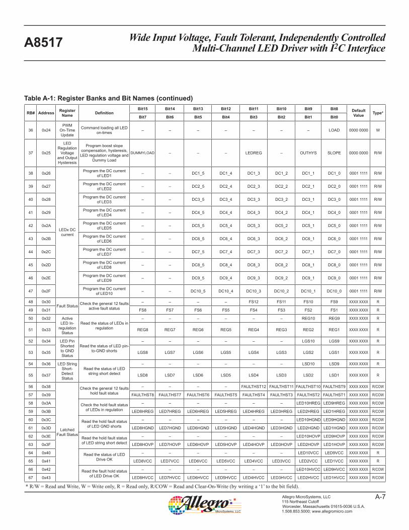
Wide Input Voltage, Fault Tolerant, Independently Controlled Multi-Channel LED Driver with I2C InterfaceA8517
A-7Allegro MicroSystems, LLC115 Northeast CutoffWorcester, Massachusetts 01615-0036 U.S.A.1.508.853.5000; www.allegromicro.com
RB# Address Register Name Definition
Bit15 Bit14 Bit13 Bit12 Bit11 Bit10 Bit9 Bit8 Default Value Type*
Bit7 Bit6 Bit5 Bit4 Bit3 Bit2 Bit1 Bit0
36 0x24PWM
On-Time Update
Command loading all LED on-times – – – – – – – LOAD 0000 0000 W
37 0x25
LED Regulation
Voltage and Output Hysteresis
Program boost slope compensation, hysteresis, LED regulation voltage and
Dummy Load
DUMMYLOAD – – – LEDREG – OUTHYS SLOPE 0000 0000 R/W
38 0x26
LEDx DC current
Program the DC current of LED1 – – DC1_5 DC1_4 DC1_3 DC1_2 DC1_1 DC1_0 0001 1111 R/W
39 0x27 Program the DC current of LED2 – – DC2_5 DC2_4 DC2_3 DC2_2 DC2_1 DC2_0 0001 1111 R/W
40 0x28 Program the DC current of LED3 – – DC3_5 DC3_4 DC3_3 DC3_2 DC3_1 DC3_0 0001 1111 R/W
41 0x29 Program the DC current of LED4 – – DC4_5 DC4_4 DC4_3 DC4_2 DC4_1 DC4_0 0001 1111 R/W
42 0x2A Program the DC current of LED5 – – DC5_5 DC5_4 DC5_3 DC5_2 DC5_1 DC5_0 0001 1111 R/W
43 0x2B Program the DC current of LED6 – – DC6_5 DC6_4 DC6_3 DC6_2 DC6_1 DC6_0 0001 1111 R/W
44 0x2C Program the DC current of LED7 – – DC7_5 DC7_4 DC7_3 DC7_2 DC7_1 DC7_0 0001 1111 R/W
45 0x2D Program the DC current of LED8 – – DC8_5 DC8_4 DC8_3 DC8_2 DC8_1 DC8_0 0001 1111 R/W
46 0x2E Program the DC current of LED9 – – DC9_5 DC9_4 DC9_3 DC9_2 DC9_1 DC9_0 0001 1111 R/W
47 0x2F Program the DC current of LED10 – – DC10_5 DC10_4 DC10_3 DC10_2 DC10_1 DC10_0 0001 1111 R/W
48 0x30Fault Status Check the general 12 faults
active fault status– – – – FS12 FS11 FS10 FS9 XXXX XXXX R
49 0x31 FS8 FS7 FS6 FS5 FS4 FS3 FS2 FS1 XXXX XXXX R
50 0x32 Active LED In-
regulation Status
Read the status of LEDs in regulation
– – – – – – REG10 REG9 XXXX XXXX R
51 0x33 REG8 REG7 REG6 REG5 REG4 REG3 REG2 REG1 XXXX XXXX R
52 0x34 LED Pin Shorted to GND Status
Read the status of LED pin-to-GND shorts
– – – – – – LGS10 LGS9 XXXX XXXX R
53 0x35 LGS8 LGS7 LGS6 LGS5 LGS4 LGS3 LGS2 LGS1 XXXX XXXX R
54 0x36 LED String Short-Detect Status
Read the status of LED string short detect
– – – – – – LSD10 LSD9 XXXX XXXX R
55 0x37 LSD8 LSD7 LSD6 LSD5 LSD4 LSD3 LSD2 LSD1 XXXX XXXX R
56 0x38
Latched Fault Status
Check the general 12 faults hold fault status
– – – – FAULTHST12 FAULTHST11 FAULTHST10 FAULTHST9 XXXX XXXX R/COW
57 0x39 FAULTHST8 FAULTHST7 FAULTHST6 FAULTHST5 FAULTHST4 FAULTHST3 FAULTHST2 FAULTHST1 XXXX XXXX R/COW
58 0x3A Check the hold fault status of LEDs in regulation
– – – – – – LED10HREG LED9HREG XXXX XXXX R/COW
59 0x3B LED8HREG LED7HREG LED6HREG LED5HREG LED4HREG LED3HREG LED2HREG LED1HREG XXXX XXXX R/COW
60 0x3C Read the hold fault status of LED GND shorts
– – – – – – LED10HGND LED9HGND XXXX XXXX R/COW
61 0x3D LED8HGND LED7HGND LED6HGND LED5HGND LED4HGND LED3HGND LED2HGND LED1HGND XXXX XXXX R/COW
62 0x3E Read the hold fault status of LED string short detect
– – – – – – LED10HOVP LED9HOVP XXXX XXXX R/COW
63 0x3F LED8HOVP LED7HOVP LED6HOVP LED5HOVP LED4HOVP LED3HOVP LED2HOVP LED1HOVP XXXX XXXX R/COW
64 0x40 Read the status of LED Drive OK
– – – – – – LED10VCC LED9VCC XXXX XXXX R
65 0x41 LED8VCC LED7VCC LED6VCC LED5VCC LED4VCC LED3VCC LED2VCC LED1VCC XXXX XXXX R
66 0x42 Read the fault hold status of LED Drive OK
– – – – – – LED10HVCC LED9HVCC XXXX XXXX R/COW
67 0x43 LED8HVCC LED7HVCC LED6HVCC LED5HVCC LED4HVCC LED3HVCC LED2HVCC LED1HVCC XXXX XXXX R/COW
* R/W = Read and Write, W = Write only, R = Read only, R/COW = Read and Clear-On-Write (by writing a ‘1’ to the bit field).
Table A-1: Register Banks and Bit Names (continued)

Wide Input Voltage, Fault Tolerant, Independently Controlled Multi-Channel LED Driver with I2C InterfaceA8517
A-8Allegro MicroSystems, LLC115 Northeast CutoffWorcester, Massachusetts 01615-0036 U.S.A.1.508.853.5000; www.allegromicro.com
LED EnableAddress: 0x00:0x01
RB RB0 (0x00) RB1 (0x01)Bit 15 14 13 12 11 10 9 8 7 6 5 4 3 2 1 0
Name – – – – – – LED ENABLE_M LED Enable_L
R/W R/W R/W R/W R/W R/W R/W R/W R/W R/W R/W R/W R/W R/W R/W R/W R/W
Value X X X X X X 0/1 0/1 0/1 0/1 0/1 0/1 0/1 0/1 0/1 0/1
Reset 0 0 0 0 0 0 1 1 1 1 1 1 1 1 1 1
MSB = Bit 9
LED Enable_M [9:8]LED Enable Settings (MSB Byte)Enables or disables LED strings 9 to 10.
Bit Value Description
90 Disable LED10
1 Enable LED10 (default)
80 Disable LED9
1 Enable LED9 (default)
LED Enable_L [7:0]LED Enable Settings (LSB Byte)Enables or disables LED strings 1 to 8.
Bit Value Description
70 Disable LED8
1 Enable LED8 (default)
60 Disable LED7
1 Enable LED7 (default)
50 Disable LED6
1 Enable LED6 (default)
40 Disable LED5
1 Enable LED5 (default)
30 Disable LED4
1 Enable LED4 (default)
20 Disable LED3
1 Enable LED3 (default)
10 Disable LED2
1 Enable LED2 (default)
00 Disable LED1
1 Enable LED1 (default)
Note:If any LED is unpopulated (signalled by having a 4.7 kΩ resistor from the LEDx pin to GND) , but
during startup it is incorrectly set to Enable in this register, the IC considers this an error and will not
proceed with startup. This is summarized in the following table:
LED String Hardware
Status
Register (RB0+1 Enable
StatusLED LIght Fault Flag
Populated Disabled Off High (no fault)
Enabled On High (no fault)
Unpopulated (4.7 kΩ resistor
to GND)
Disabled Off High (no fault)
Enabled Off Low (fault)
Register Field Reference

Wide Input Voltage, Fault Tolerant, Independently Controlled Multi-Channel LED Driver with I2C InterfaceA8517
A-9Allegro MicroSystems, LLC115 Northeast CutoffWorcester, Massachusetts 01615-0036 U.S.A.1.508.853.5000; www.allegromicro.com
LED PWM PeriodAddress: 0x02:0x03
RB RB2 (0x02) RB3 (0x03)Bit 15 14 13 12 11 10 9 8 7 6 5 4 3 2 1 0
Name – – – PWM_Period_H PWM_Period_L
R/W R/W R/W R/W R/W R/W R/W R/W R/W R/W R/W R/W R/W R/W R/W R/W R/W
Value X X X 0/1 0/1 0/1 0/1 0/1 0/1 0/1 0/1 0/1 0/1 0/1 0/1 0/1
Reset 0 0 0 0 1 1 1 1 1 1 1 1 1 1 1 1
MSB = Bit 12
This register allows the user to set a wide variety of PWM dim-ming periods. Bit resolution is 1.5 µs. The actual PWM period is defined as (N+1) × 1.5 µs, where N is the combined value stored in these two register banks. A 13-bit total programming capabil-ity allows the user program up to approximately a 10 ms PWM period (a 100 Hz PWM frequency).
The smallest recommended PWM period is 45 µs ( 22 kHz PWM frequency). The maximum recommended PWM period is 9.830 ms, which corresponds to a setting of XXX1 1001 1001 1000 (calculated as: (6552+1) × 1.5 µs = 9.8295 ms).
It is possible for the user to program a longer PWM period, but doing so will not allow 100% PWM dimming because the LED on-time counter can be programmed only up to a maximum of 9.830 ms. So for example, if the user programs the maximum period (XXX1 1111 1111 1111), this gives a PWM period of (8191+1) × 1.5 µs = 12.288 ms, so all LEDs would be limited to an 80% PWM duty cycle.
The reset setting is 0x0fff = 4095. This corresponds to a PWM period of (4095+1) × 1.5 µs = 6.144 ms (162.8 Hz PWM fre-quency).
Example: To set the PWM frequency to 400 Hz:
1. PWM period = 1/400 = 2.5 ms2. Number of steps = 2.5 ms / 1.5 µs = 16673. The required LED PWM_Period register value is then 1666
(XXX0 0110 1000 0010): RB2 = 0000 0110 (MSB)
RB3 = 1000 0010 (LSB)
PWM_Period_H [12:8]PWM Dimming Period (MSB Byte) PWM_Period_L [7:0]PWM Dimming Period (LSB Byte)
Bit Value Description
12:0 0/1 Absolute PWM period multiplier

Wide Input Voltage, Fault Tolerant, Independently Controlled Multi-Channel LED Driver with I2C InterfaceA8517
A-10Allegro MicroSystems, LLC115 Northeast CutoffWorcester, Massachusetts 01615-0036 U.S.A.1.508.853.5000; www.allegromicro.com
OVP ThresholdAddress: 0x04
RB RB4 (0x04)
Bit 7 6 5 4 3 2 1 0
Name – – – OVP
R/W R/W R/W R/W R/W R/W R/W R/W R/W
Value X X X 0/1 0/1 0/1 0/1 0/1
Reset 0 0 0 1 1 1 0 0
MSB = Bit 4
Boost Dithering and Thermal DeratingAddress: 0x05
RB RB5 (0x05)Bit 7 6 5 4 3 2 1 0
Name – – – – – TD BD1 BD0
R/W R/W R/W R/W R/W R/W R/W R/W R/W
Value X X X X X 0/1 0/1 0/1
Reset 0 0 0 0 0 0 0 0
MSB = Bit 2
BDx [1:0]Boost Dither Enable and MagnitudeEnable and set the multiplier for the main switching frequency dithering feature. Not available when external synchronization signal is used (through FSET/SYNC pin). Example: Value of 11 sets ±15% (step size x number of steps = 5% × 3). If fSW = 600 kHz, ±90 kHz: lower frequency = 510 kHz, upper frequency = 690 kHz.
BitDescription
BD1 BD0
0 0 Disable dithering (default)
0 1 Frequency variation ±5% of nominal fSW
1 0 Frequency variation ±10% of nominal fSW
1 1 Frequency variation ±15% of nominal fSW
TD [2]LED Derating EnableEnables the Thermal Derating function.
Bit Value Description
20 Disable Thermal Derating feature (default)
1 Enable Thermal Derating
OVP [4:0]OVP Trip PointSets the OVP trip point multiplier. Bit resolution is 1.0 V. The OVP trip point can be set anywhere from 8 V (00000) to 39 V (11111). Example: The reset value of 0x1C, 28 decimal, gives an OVP trip point of: 8 V + (1.0 V × 28) = 36 V.
Bit Value Description
4:0 0/1 Sets the OVP threshold multiplier

Wide Input Voltage, Fault Tolerant, Independently Controlled Multi-Channel LED Driver with I2C InterfaceA8517
A-11Allegro MicroSystems, LLC115 Northeast CutoffWorcester, Massachusetts 01615-0036 U.S.A.1.508.853.5000; www.allegromicro.com
Fault ModeAddress: 0x06:0x07
RB RB6 (0x06) RB7 (0x07)Bit 15 14 13 12 11 10 9 8 7 6 5 4 3 2 1 0
Name – – – – FAULT CNTRL_M FAULT CNTRL_L
R/W R/W R/W R/W R/W R/W R/W R/W R R/W R R R/W R R/W R/W R
Value X X X X 0/1 0/1 0/1 0 0/1 0 1 0/1 1 0/1 0/1 0
Reset 0 0 0 0 1 0 1 0 1 0 1 1 1 1 1 0
MSB = Bit 11
FAULT CNTRL_M [11:8]Fault Control Mode Settings (MSB Byte)Sets the fault handling behavior for faults 9 through 12. Certain bits are non-programmable (default value only) for safety reasons.
Bit Value Description
110 Fault 12 Latched (no auto restart)
1 Fault 12 Auto restart (default)
100 Fault 11 Latched (no auto restart) (default)
1 Fault 11 Auto restart
90 Fault 10 Latched (no auto restart)
1 Fault 10 Auto restart (default)
8 0 Fault 9 Latched (no auto restart) (default)
FAULT CNTRL_L [7:0]Fault Control Mode Settings (LSB Byte)Sets the fault handling behavior for faults 8 through 1. Certain bits are non-programmable (default value only) for safety reasons.
Bit Value Description
70 Fault 8 Latched (no auto restart)
1 Fault 8 Auto restart (default)
6 0 Fault 7 Latched (no auto restart) (default)
5 1 Fault 6 Auto restart (default)
40 Fault 5 Latched (no auto restart)
1 Fault 5 Auto restart (default)
3 1 Fault 4 Auto restart (default)
20 Fault 3 Latched (no auto restart)
1 Fault 3 Auto restart (default)
10 Fault 2 Latched (no auto restart)
1 Fault 2 Auto restart (default)
0 0 Fault 1 Latched (no auto restart) (default)
Wide Input Voltage, Fault Tolerant, Independently Controlled Multi-Channel LED Driver with I2C InterfaceA8517
A-12Allegro MicroSystems, LLC115 Northeast CutoffWorcester, Massachusetts 01615-0036 U.S.A.1.508.853.5000; www.allegromicro.com
Polyphase GroupingAddress: 0x08:0x09
RB RB8 (0x08) RB9 (0x09)Bit 15 14 13 12 11 10 9 8 7 6 5 4 3 2 1 0
Name – – – – – – – POLYPHASE_M POLYPHASE_L
R/W R/W R/W R/W R/W R/W R/W R/W R/W R/W R/W R/W R/W R/W R/W R/W R/W
Value X X X X X X X 0/1 0/1 0/1 0/1 0/1 0/1 0/1 0/1 0/1
Reset 0 0 0 0 0 0 0 0 0 0 0 0 0 0 0 0
MSB = Bit 8
POLYPHASE_M [8]LED String Grouping (MSB Byte)
Enables grouping with LED10.
Bit Value Description
80 LED10 not grouped (default)
1 LED10 grouped
POLYPHASE_L [7:0]LED String Grouping (LSB Byte)Enables grouping with LED10 through LED2. Note: LED1 is not included, because there is no lower-number LED channel, but it can be grouped by setting LED2.
Bit Value Description
70 LED9 not grouped (default)
1 LED9 grouped
60 LED8 not grouped (default)
1 LED8 grouped
50 LED7 not grouped (default)
1 LED7 grouped
40 LED6 not grouped (default)
1 LED6 grouped
30 LED5 not grouped (default)
1 LED5 grouped
20 LED4 not grouped (default)
1 LED4 grouped
10 LED3 not grouped (default)
1 LED3 grouped
00 LED2 not grouped (default)
1 LED2 grouped
An ungrouped LED channel starts PWM operation in a separate time slot, with duty cycle specified by the corresponding PWM Dimming On-Time register.
A grouped LED channel starts in the same time slot as the next lower-numbered channel, and inherits the PWM Dimming On-Time of that lower-numbered channel (the original time slot of the grouped channel is not used). If more than one adjacent channels are grouped, the entire group starts at the time slot of the lowest-numbered channel in the group, and inherits that on-time setting. Example: Set bit 6 to group LED8 with LED7 (start and duty cycle according to LED7), also set bit 5 to group LED8 and LED7 with LED6 (start and duty cycle according to LED6).

Wide Input Voltage, Fault Tolerant, Independently Controlled Multi-Channel LED Driver with I2C InterfaceA8517
A-13Allegro MicroSystems, LLC115 Northeast CutoffWorcester, Massachusetts 01615-0036 U.S.A.1.508.853.5000; www.allegromicro.com
LED Short-Detect ThresholdAddress: 0x0A: 0x0E
RB RB10 (0x0A) to RB14 (0x0E)Bit 7 6 5 4 3 2 1 0
RB10 – SDT2_x – SDT1_x
RB11 – SDT4_x – SDT3_x
RB12 – SDT6_x – SDT5_x
RB13 – SDT8_x – SDT7_x
RB14 – SDT10_x – SDT9_x
R/W R/W R/W R/W R/W R/W R/W R/W R/W
Value X 0/1 0/1 0/1 0/1 0/1 0/1 0/1
Reset 0 0 0 0 0 0 0 0
MSB = Bit 6 and bit 2
SDTx_x [6:4], [2:0]LED String Short Detect ThresholdAllows adjustment of the LED string short-detect threshold for each LED channel to prevent false tripping if the voltage drop across all LED strings varies by more than one LED Vf during normal operation.
Bit
Description6 5 4
2 1 0
0 0 0 Threshold = 12 V (default)
0 0 1 Threshold = 11 V
0 1 0 Threshold = 10 V
0 1 1 Threshold = 9 V
1 0 0 Threshold = 8 V
1 0 1 Threshold = 7 V
1 1 0 Threshold = 6 V
1 1 1 Threshold = 5 V
Wide Input Voltage, Fault Tolerant, Independently Controlled Multi-Channel LED Driver with I2C InterfaceA8517
A-14Allegro MicroSystems, LLC115 Northeast CutoffWorcester, Massachusetts 01615-0036 U.S.A.1.508.853.5000; www.allegromicro.com
General Purpose Output SelectionAddress: 0x0F
RB RB15 (0x0F)Bit 7 6 5 4 3 2 1 0
Name – – – GPO1 – GPO2
R/W R/W R/W R/W R/W R/W R/W R/W R/W
Value X X X 0/1 0/1 X 0/1 0/1
Reset 0 0 0 0 0 0 0 0
MSB = Bit 4, bit 1
GPO2 [1:0]General Purpose Output 2 Data
Select data type to be output on the GPO2 pin.
BitDescription
1 0
0 0Data: IC and LED status (default) High = startup test not passed
Low = LED startup test passed
0 1Data: SW 1x Current Limit High = normal operation
Low = current limit exceeded
1 0Data: Boost status
High = Boost switching Low = No switching
1 1 Reserved
GPO1 [4:3]General Purpose Output 1 Data
Select data type to be output on the GPO1 pin.
BitDescription
4 3
0 0Data: Boost soft start status (default)
High = soft start in progress Low = soft start finished
0 1 Data: Master system clock / 4 Normal operation = approximately 1.65 MHz
1 0Data: LED PWM frequency
Normal operation = low approximately 300 ns each PWM period)
1 1Data: Thermal Warning
High = normal operation Low = Thermal Derating active

Wide Input Voltage, Fault Tolerant, Independently Controlled Multi-Channel LED Driver with I2C InterfaceA8517
A-15Allegro MicroSystems, LLC115 Northeast CutoffWorcester, Massachusetts 01615-0036 U.S.A.1.508.853.5000; www.allegromicro.com
PWM Dimming On-TimeAddress: 0x10:0x23
Bit 15 14 13 12 11 10 9 8 7 6 5 4 3 2 1 0RB RB16 (0x10) RB17 (0x11)
Name LED1_TON_M LED1_TON_L
RB RB18 (0x12) RB19 (0x13)
Name LED2_TON_M LED2_TON_L
RB RB20 (0x14) RB21 (0x15)
Name LED3_TON_M LED3_TON_L
RB RB22 (0x16) RB23 (0x17)
Name LED4_TON_M LED4_TON_L
RB RB24 (0x18) RB25 (0x19)
Name LED5_TON_M LED5_TON_L
RB RB26 (0x1A) RB27 (0x1B)
Name LED6_TON_M LED6_TON_L
RB RB28 (0x1C) RB29 (0x1D)
Name LED7_TON_M LED7_TON_L
RB RB30 (0x1E) RB31 (0x1F)
Name LED8_TON_M LED8_TON_L
RB RB33 (0x20) RB33 (0x21)
Name LED9_TON_M LED9_TON_L
RB RB34 (0x22) RB35 (0x23)
Name LED10_TON_M LED10_TON_L
R/W R/W R/W R/W R/W R/W R/W R/W R/W R/W R/W R/W R/W R/W R/W R/W R/W
Value X X X X X X X 0/1 0/1 0/1 0/1 0/1 0/1 0/1 0/1 0/1
Reset 0 0 0 0 0 0 0 0 0 0 0 0 0 0 0 0
MSB = Bit 15
Set PWM dimming on-time multiplier for each LED channel. 16 bits are required for each channel. Bit resolution is 150 ns.
Let T = LED PWM Period, and tON = PWM Dimming On-Time, then the PWM dimming percentage = tON / T.
Although the minimum on-time that can be set by the register is 150 ns, in practice it is strongly advised to keep the on-time at 1 µs or above. This implies a maximum dimming ratio of 5000:1 at 200 Hz PWM frequency. Therefore, the minimum tON multiplier is 7 (0000 0000 0000 0111 in binary), which gives 150 ns × 7 = 1.05 µs.
The maximum tON multiplier is 65,535 (1111 1111 1111 1111 in binary), which gives 150 ns × 65,535 = 9.83 ms. When all 16 bits are 1, or when tON > T , the LEDs are on all the time.
The default register value = 0x0000, which means all LED chan-nels are off, even if they are enabled by RB0 and RB1. Therefore it is necessary to update the LED on-time registers first, in order to turn on LED strings.
The registers must be written as MSB followed by LSB. Update is allowed only after LSB write is complete. All ten registers are buffered initially, until a Write operation is performed on register 0x24, at which time all 10 channels are updated together.
LEDx_TON_M [15:8]LED PWM On-Time (MSB Byte) LEDx_TON_L [7:0]LED PWM On-Time (LSB Byte)
Bit Value Description
15:0 0/1 Absolute PWM on-time multiplier

Wide Input Voltage, Fault Tolerant, Independently Controlled Multi-Channel LED Driver with I2C InterfaceA8517
A-16Allegro MicroSystems, LLC115 Northeast CutoffWorcester, Massachusetts 01615-0036 U.S.A.1.508.853.5000; www.allegromicro.com
PWM On-Time UpdateAddress: 0x24
RB RB36 (0x24)Bit 7 6 5 4 3 2 1 0
Name – – – – – – – LOAD
R/W W W W W W W W R/W
Value 0/1 0/1 0/1 0/1 0/1 0/1 0/1 0/1
Reset 0 0 0 0 0 0 0 0
MSB = Bit 0
LOAD [0]Enable Load PWM On-Time UpdateAll PWM on-time registers are buffered and do not take effect until a Write operation is performed on register 0x24 (the actual data written does not matter). When the write operation is complete, all 10 channel data are updated together. This feature is vital for applications that require synchronized update for all LED brightness, such as for localized dimming.
Bit Value Description
00 (default)
1 Upload current contents of PWM dimming on-time registers
Wide Input Voltage, Fault Tolerant, Independently Controlled Multi-Channel LED Driver with I2C InterfaceA8517
A-17Allegro MicroSystems, LLC115 Northeast CutoffWorcester, Massachusetts 01615-0036 U.S.A.1.508.853.5000; www.allegromicro.com
LED Regulation Voltage and Output HysteresisAddress: 0x25
RB RB37 (0x25)Bit 7 6 5 4 3 2 1 0
Name DUMMYLOAD – – – LEDREG – OUTHYS SLOPE
R/W R/W R/W R/W R/W R/W R/W R/W R/W
Value 0/1 0/1 0/1 0/1 0/1 0/1 0/1 0/1
Reset 0 0 0 0 0 0 0 0
MSB = Bit 7
DUMMYLOAD [7]Enable Startup Output Load ResistanceEnables a resistive load of approximately 4.3 kΩ connected to VOUT during startup process. The load is removed after startup is completed.
Bit Value Description
70 (default)
1 Enable connection of resistive load
OUTHYS [1]Enable Augmented Output HysteresisThe A8517 has a minimum output voltage hysteresis of 0.25 V. Lower hysteresis is generally preferred, because excessive ripple voltage may lead to audible noises from output ceramic capacitors. But larger ripple may be required to reduce the frequency of the hysteresis control loop. The correct value should be determined through experimentation.
Bit Value Description
10 Normal VOUThys, 0.25 V (typ) recommended
(default)
1 Augmented VOUThys, 0.45 V
LEDREG [3]Enable Augmented LED Regulation VoltageThe A8517 has a minimum LED Regulation voltage of 0.85 V (typ). Lower regulation voltage is generally preferred, because it means less power loss across the LEDx current sinks. In certain situations (such as during input voltage transients at extremely low PWM duty cycles) it may be advantageous to set the regulation voltage higher in order to maintain current regulation.
Bit Value Description
30 Normal VREG, 0.85 V (typ) (default)
1 Augmented VREG, 1.05 V
SLOPE [0]Enable Reduced Slope CompensationSlope compensation is necessary in current-mode control circuits in order to avoid instability at > 50% SW duty cycle. The A8517 allows selection between two slope compensation values for best results.
Bit Value Description
00 10.8 A / µs at 2 MHz
1 2.3 A / µs at 2 Mz

Wide Input Voltage, Fault Tolerant, Independently Controlled Multi-Channel LED Driver with I2C InterfaceA8517
A-18Allegro MicroSystems, LLC115 Northeast CutoffWorcester, Massachusetts 01615-0036 U.S.A.1.508.853.5000; www.allegromicro.com
LEDx DC CurrentAddress: 0x26: 0x2F
Bit 7 6 5 4 3 2 1 0RB RB38 (0x26)
Name – – LED1_CURRENT
RB RB39 (0x27)
Name – – LED2_CURRENT
RB RB40 (0x28)
Name – – LED3_CURRENT
RB RB41 (0x29)
Name – – LED4_CURRENT
RB RB42 (0x2A)
Name – – LED5_CURRENT
RB RB43 (0x2B)
Name – – LED6_CURRENT
RB RB44 (0x2C)
Name – – LED7_CURRENT
RB RB45 (0x2D)
Name – – LED8_CURRENT
RB RB46 (0x2E)
Name – – LED9_CURRENT
RB RB47 (0x2F)
Name – – LED10_CURRENT
R/W R/W R/W R/W R/W R/W R/W R/W R/W
Value 0/1 0/1 0/1 0/1 0/1 0/1 0/1 0/1
Reset 0 0 0 1 1 1 1 1
MSB = Bit 5
LEDx_CURRENT [5:0]LED Current Sink Capacity Sets DC sink current capability multiplier for each LED channel. Bit resolution is 1 mA. Each LED channel has a base current of 1 mA. Default is 0x1F = 32 mA.
Bit Value Description
5:0 0/1 Absolute LED current multiplier
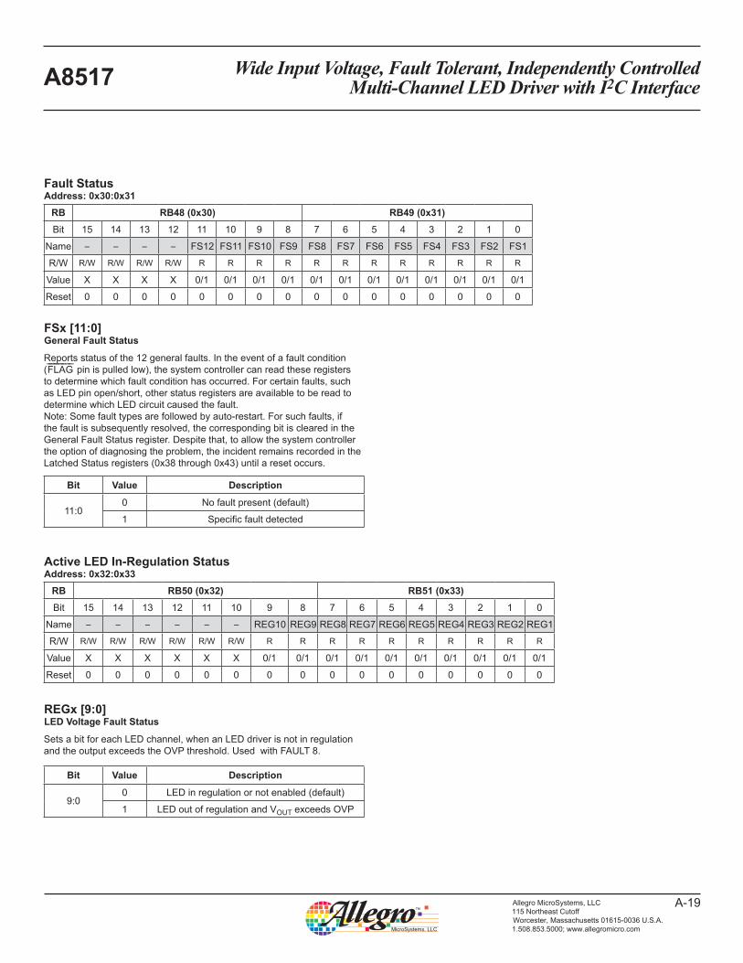
Wide Input Voltage, Fault Tolerant, Independently Controlled Multi-Channel LED Driver with I2C InterfaceA8517
A-19Allegro MicroSystems, LLC115 Northeast CutoffWorcester, Massachusetts 01615-0036 U.S.A.1.508.853.5000; www.allegromicro.com
Fault StatusAddress: 0x30:0x31
RB RB48 (0x30) RB49 (0x31)Bit 15 14 13 12 11 10 9 8 7 6 5 4 3 2 1 0
Name – – – – FS12 FS11 FS10 FS9 FS8 FS7 FS6 FS5 FS4 FS3 FS2 FS1
R/W R/W R/W R/W R/W R R R R R R R R R R R R
Value X X X X 0/1 0/1 0/1 0/1 0/1 0/1 0/1 0/1 0/1 0/1 0/1 0/1
Reset 0 0 0 0 0 0 0 0 0 0 0 0 0 0 0 0
Active LED In-Regulation StatusAddress: 0x32:0x33
RB RB50 (0x32) RB51 (0x33)Bit 15 14 13 12 11 10 9 8 7 6 5 4 3 2 1 0
Name – – – – – – REG10 REG9 REG8 REG7 REG6 REG5 REG4 REG3 REG2 REG1
R/W R/W R/W R/W R/W R/W R/W R R R R R R R R R R
Value X X X X X X 0/1 0/1 0/1 0/1 0/1 0/1 0/1 0/1 0/1 0/1
Reset 0 0 0 0 0 0 0 0 0 0 0 0 0 0 0 0
FSx [11:0]General Fault Status
Reports status of the 12 general faults. In the event of a fault condition (F L A G pin is pulled low), the system controller can read these registers to determine which fault condition has occurred. For certain faults, such as LED pin open/short, other status registers are available to be read to determine which LED circuit caused the fault. Note: Some fault types are followed by auto-restart. For such faults, if the fault is subsequently resolved, the corresponding bit is cleared in the General Fault Status register. Despite that, to allow the system controller the option of diagnosing the problem, the incident remains recorded in the Latched Status registers (0x38 through 0x43) until a reset occurs.
Bit Value Description
11:00 No fault present (default)
1 Specific fault detected
REGx [9:0]LED Voltage Fault Status
Sets a bit for each LED channel, when an LED driver is not in regulation and the output exceeds the OVP threshold. Used with FAULT 8.
Bit Value Description
9:00 LED in regulation or not enabled (default)
1 LED out of regulation and VOUT exceeds OVP

Wide Input Voltage, Fault Tolerant, Independently Controlled Multi-Channel LED Driver with I2C InterfaceA8517
A-20Allegro MicroSystems, LLC115 Northeast CutoffWorcester, Massachusetts 01615-0036 U.S.A.1.508.853.5000; www.allegromicro.com
LED Pin Shorted to GND StatusAddress: 0x34:0x35
RB RB52 (0x34) RB53 (0x35)Bit 15 14 13 12 11 10 9 8 7 6 5 4 3 2 1 0
Name – – – – – – LGS10 LGS9 LGS8 LGS7 LGS6 LGS5 LGS4 LGS3 LGS2 LGS1
R/W R/W R/W R/W R/W R/W R/W R R R R R R R R R R
Value X X X X X X 0/1 0/1 0/1 0/1 0/1 0/1 0/1 0/1 0/1 0/1
Reset 0 0 0 0 0 0 0 0 0 0 0 0 0 0 0 0
LED String Short-Detect StatusAddress: 0x36:0x37
RB RB53 (0x36) RB54 (0x37)Bit 15 14 13 12 11 10 9 8 7 6 5 4 3 2 1 0
Name – – – – – – LSD10 LSD9 LSD8 LSD7 LSD6 LSD5 LSD4 LSD3 LSD2 LSD1
R/W R/W R/W R/W R/W R/W R/W R R R R R R R R R R
Value X X X X X X 0/1 0/1 0/1 0/1 0/1 0/1 0/1 0/1 0/1 0/1
Reset 0 0 0 0 0 0 0 0 0 0 0 0 0 0 0 0
Latched Status RegistersAddress: 0x38:0x43(RB56 to RB67)
LGSx [9:0]LED Short to GND Fault Status
This bit is set if an LED pin voltage is found to remain at GND level during startup (prevents further initialization). Used with FAULT 10.
Bit Value Description
9:00 LED voltage normal (default)
1 LED remaining at GND during startup
LSDx [9:0]LED String Short Detect Status
This bit is set if an LED pin voltage goes above its preset voltage limit, as set by its corresponding LED pin Short-Detect Threshold register. Used with FAULT 12.
Bit Value Description
9:00 LED voltage normal (default)
1 LED exceeds short-detect threshold
Retain the status of faults that have been detected, allowing the system controller to poll them by an I2C Read to diagnose problems. All bits are cleared after a Read for the register.

Wide Input Voltage, Fault Tolerant, Independently Controlled Multi-Channel LED Driver with I2C InterfaceA8517
B-1Allegro MicroSystems, LLC115 Northeast CutoffWorcester, Massachusetts 01615-0036 U.S.A.1.508.853.5000; www.allegromicro.com
APPENDIX B: FEEDBACK LOOP COMPONENTS CALCULATION FOR PEAK CURRENT CONTROL BOOST CONVERTER USED IN LED DRIVERS APPLICATIONSThis appendix provides an examination of the factors involved in calculating the transfer function of a peak current controlled boost converter, an output to control transfer function, and rec-ommendations for stabilizing the feedback loop closed system. An example of a complete small signal model of a peak-current-mode boost converter is shown in Figure B-2. The A8517 is an example of a boost converter that drives 10 LED strings with 10 LEDs in each string.
Power Stage Transfer FunctionUsing a frequency-based model, the transfer function (control to output) of boost power stage peak-current control is given by the following equation:
×1+2 × × f × j
ωZ
1–2 × × f × j
ωRHP
×1+2 × × f × j
ωP
1+2 × × f × j
Q ×D ωS
+(2 × × f × j) 2
ωS
2
T (f ) = A ×P P (B-1)
AP is the DC gain,
ωZ is the angular frequency of the output capacitor ESR zero, fZ ,
ωRHP is the angular frequency of the right-half plane zero, fRHP ,
ωP is the angular frequency of the output load pole, fP ,
QD is the inductor peak current sampling double pole quality or damping factor, and
ωS is the double-pole angular frequency oscillation .
Figure A-1 shows the plot of the power stage logarithmic transfer function as gain, GP(f) , versus frequency. with GP(f) given by:
GP(f) = 20 × log( |TP(f)| ) (B-2)The next sections define the components of TP(f).
Figure B-1: Plot of Power Stage Transfer Function ver-sus Frequency
10 100 1 103 1 104 1 105 1 106 1 107 1 108
–100
0
Gai
n, G
P(f)
Frequency (Hz)× × × × × ×
AP , DC gain
The DC gain is defined as follows:
A =P ×1 D(nom)
RI
R × RS EQ
R + R + RS D EQ
(B-3)
where
• D is the PWM duty cycle, calculated as:
D(nom) = (VOUT – VIN(nom)) / VOUT (B-4)
where
VOUT = NL × Vf + VREG + VD + VH (B-5) and NL is the quantity of LEDs per string,
Vf is the nominal forward voltage drop for each LED diode,
VREG is the current sink regulated voltage for each LED string,
VD is the Schottky diode forward voltage drop and
VH is the output hysteresis-control voltage.
• RI is the current sense resistor, which is connected in series with the boost power switch,
• RS is the LED sink pin sense resistor, which is usually located inside the IC and can be calculated from the following equation:
RS = VREG / ILED (B-6)

Wide Input Voltage, Fault Tolerant, Independently Controlled Multi-Channel LED Driver with I2C InterfaceA8517
B-2Allegro MicroSystems, LLC115 Northeast CutoffWorcester, Massachusetts 01615-0036 U.S.A.1.508.853.5000; www.allegromicro.com
where ILED is the current through one LED string,
• REQ is the output nominal operating resistance, which is given by the following equation:
REQ = VOUT / ILEDT (B-7)
where ILEDT is the total output current through all LED strings:
ILEDT = NS × ILED (B-8) and NS is the total quantity of LED strings, and
• RD is the total dynamic resistance of one LED string, which can be measured in the lab, as follows:
1. Get a load board with one string of LEDs.2. Apply an external DC voltage across all LEDs in one string
through a current limit resistor, R = 10 Ω.3. Change the DC voltage to get 90% of one string current. Then
measure the voltage across all LEDs in one string.4. Repeat step 3 until reaching 100% of one string current.5. Calculate RD = ( V2 – V1 ) / ( I2 – I2 ) . V2 is the voltage across all
LEDs in one string at I2 = 100% of one string LED current. V1 is the voltage across all LEDs in one string at I1 = 90% of one string LED current.
QD , inductor peak current sampling double pole quality
Q =D × [0.5– D(nom)+ ( 1 – D(nom)) × IFSC]
1
(B-9)
where
IFSC is the implemented factor of inductor slope compensa- tion, and is given by:
IFSC = ( ISC / CSC ) × FSC (B-10)and
ISC is the IC implemented slope compensation in A/µs. At 2 MHz switching frequency, ISC = 2.3 A/µs. However, it changes as the switching frequency changes. It is normalized to a 2 MHz swtiching frequency. At a switching frequency dif-ferent from 2 MHz the implemented slope compensation can be calculated from:
ISC = 2.3 (A/µs) × ( fSW / 2 (MHz)) (B-11)
CSC is the calculated slope compensation also in A/µs, given by:
CSC =∆I FSC× × 10
–6
(1/ f )SW × (1– D(max))(B-12)
and
ΔI = (VIN(min) × D(max)) / L1 × fSW , and (B-13) FSC is the Ridley’s factor slope compensation, given by:
FSC = 1 – 0.18 / D(max) (B-14)ωZ , angular frequency of the output capacitor ESR zero, fZ
ωZ = 1 / (ESR × COUT ) (B-15)ωRHP , angular frequency of the right-half plane zero, fRHP
ωRHP = REQ / ((1 – D(max))2 × L1 ) (B-16) where
D(max) = (VOUT – VIN(min)) / VOUT (B-17)ωP , angular frequency of the output load pole, fP
ω =P (R + R + ESR) × R × CS D EQ OUT
R + R + RS D EQ
(B-18)
ωS , angular frequency oscillation of the double pole that occurs at half of the switching frequency, fSW
ωS = π × fSW (B-19)
Output to Control Transfer FunctionWhen using peak current mode control for a DC-to-DC converter, a type II PI error amplifier compensation circuit is sufficient to stabilize the converter. For controlling the current sink voltage and as a result controlling the output, the A8517 IC uses a high bandwidth transconductance amplifier, shown as A1 in Fig-ure B-2.
A transconductance amplifier is actually a voltage-controlled current source. It converts any error voltage at its input pins to a current flowing out of its output pin at VC. The transconductance gain of the error amplifier, g , is defined as:
g = IAMP / Verror (B-20)In Figure B-2, RAMP represents the output impedance of the transconductance amplifier (A1). RAMP usually has a high value and it is neglected in the calculation of the error amplifier transfer function.

Wide Input Voltage, Fault Tolerant, Independently Controlled Multi-Channel LED Driver with I2C InterfaceA8517
B-3Allegro MicroSystems, LLC115 Northeast CutoffWorcester, Massachusetts 01615-0036 U.S.A.1.508.853.5000; www.allegromicro.com
Ram p
Current SenseAmplifier
Transconductance(g) Amplifier
Vc
Cp
SlopeCompensation
A2
Adder
VIN
RI
Q1
ESR
D10
D1
L1
D2
COUT
D1
RsVreg
Cz
Rz
PWM andDriver
A1
VOUT
Figure B-2: Small signal model of a peak-current-mode boost converter; the ten strings of the A8517 are repre-sented by one string in this example
RZ, CZ , and CP represent the external Type II compensation net-work. From an AC point of view, the non-inverting pin of A1 is connected to a DC reference voltage, VREG , which is a virtual
AC ground. Therefore, the transfer function of the compensation circuit is derived as follows:
Figure B-3: Plot of error amplifier stage transfer func-tion versus frequency
10 100 1 103 1 104 1 105 1 106 1 107 1 10850
0
50
100
Frequency (Hz)
Mid-Band Gain
× × × × × ×
Gai
n, G
P(f)

Wide Input Voltage, Fault Tolerant, Independently Controlled Multi-Channel LED Driver with I2C InterfaceA8517
B-4Allegro MicroSystems, LLC115 Northeast CutoffWorcester, Massachusetts 01615-0036 U.S.A.1.508.853.5000; www.allegromicro.com
T (f ) =EA
–1 × I × Z ( f )AMP C
×VERROR
V ( f )C
V ( f )OUT
R + RS D
RS
=
(B-21)
(B-22)
applying equation A-20:
T (f ) = –1 ×EA × Z (f )C
R × gS
R +RS D
(B-23)
where
Z ( f ) =C
×1
R +Z
1
+1
R +Z
1
2 × × f × j× C Z
2× × f × j× C Z
2 × × f × j× C P
2 × × f × j× C P
(B-24)
Figure A-3 shows the logarithmic transfer function for the output to control compensation circuit, with gain, GEA(f). given by:
GEA(f) = 20 × log( |TEA(f)| ) (B-25)
The transfer function has a single pair of pole and zero in addi-tion to the pole at the origin. The pole at the origin is defined by CP and RAMP . The zero is defined by RZ and CZ . The zero frequency location is selected to compensate or cancel the power train load pole. It is defined by:
fZEA = 1 / (2 × π × RZ × CZ ) (B-26)The error amplifier pole frequency is selected to compen-sate for or cancel the power train ESR zero. This is the case if the frequency of the ESR zero is small or below the switch-ing frequency. Otherwise, it is selected to be at half switching frequency. This pole frequency determines the end of mid-band gain of the error amplifier transfer function, so it ensures that the closed loop system cross-over frequency is below half switch-ing frequency, which is important for stability issues. The pole frequency is defined by:
fPEA =
1
2 × × R × Z
C × CZ P
C + CZ P
(B-27)
Stabilizing the Closed Loop SystemIn this section, calculations are provided for selecting optimal RZ , CZ , and CP . The closed loop system will be stable if the total system transfer function rolls off while crossing over at a phase margin of approximately 90° or –20 dB per decade. It is recom-mended that the phase margin does not fall below 45°. For higher stability, the cross over frequency should be much less than the right half plane zero and smaller than half of the switching frequency.
To achieve that, first fix the mid-band gain of the error amplifier transfer function. Make it equal in value to the power train gain at the cross over frequency, but negative so the total closed loop gain will be 0 dB. Then position the compensation pole and zero. Here are step-by-step procedures on how to calculate the com-pensation network components:
1. Calculate RZ such that the negative mid-band gain of the error amplifier will be equal to the power train gain at the required system bandwidth or cross over frequency. A. Calculate the cross over frequency to be much less than
the RHP zero and lower than the half-switching frequen-

Wide Input Voltage, Fault Tolerant, Independently Controlled Multi-Channel LED Driver with I2C InterfaceA8517
B-5Allegro MicroSystems, LLC115 Northeast CutoffWorcester, Massachusetts 01615-0036 U.S.A.1.508.853.5000; www.allegromicro.com
10 100 1 103 1 104 1 105 1 106 1 107 1 108
100
0
100
Frequency (Hz)
× × × × × ×
Gai
n, G
S(f)
Figure B-4: Plot of the Whole System Closed Loop Transfer Function Gain versus Frequency, with a Cross Over Frequency, fC , of 30 kHz
cy. A 20 to 30 kHz cross over frequency is appropriate for LED applications, calculated as follows:
fC = 0.015 × fSW (B-28)
B. Calculate, or preferably measure, the power train gain at fC , which is GP(fC ), then multiply it by –1.
C. To compensate for the difference from the error ampli-fier gain at fZEA and the actual mid-band gain, subtract an
additional 3 dB:
–GP(fC) –3 dB (B-29)
D. Convert the calculated gain to a linear gain:
10
G ( f ) –3P C
20
(B-30)
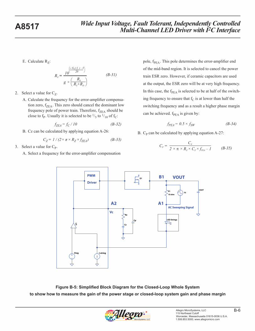
Wide Input Voltage, Fault Tolerant, Independently Controlled Multi-Channel LED Driver with I2C InterfaceA8517
B-6Allegro MicroSystems, LLC115 Northeast CutoffWorcester, Massachusetts 01615-0036 U.S.A.1.508.853.5000; www.allegromicro.com
E. Calculate RZ:
RZ =
g ×RS
R +RS D
10
– G ( f ) –3P C
20
(B-31)
2. Select a value for CZ. A. Calculate the frequency for the error-amplifier compensa-
tion zero, fZEA . This zero should cancel the dominant low frequency pole of power train. Therefore, fZEA should be close to fP . Usually it is selected to be 1/5 to 1/10 of fC:
fZEA = fC / 10 (B-32)
B. Cz can be calculated by applying equation A-26:
CZ = 1 / (2 × π × RZ × fZEA ) (B-33)
3. Select a value for CP .A. Select a frequency for the error-amplifier compensation
pole, fPEA . This pole determines the error-amplifier end
of the mid-band region. It is selected to cancel the power
train ESR zero. However, if ceramic capacitors are used
at the output, the ESR zero will be at very high frequency.
In this case, the fPEA is selected to be at half of the switch-
ing frequency to ensure that fC is at lower than half the
switching frequency and as a result a higher phase margin
can be achieved. fPEA is given by:
fPEA = 0.5 × fSW (B-34)
B. CP can be calculated by applying equation A-27:
2 × × R × C × f – 1 Z Z PEA
CZC =P
(B-35)
+–
+ –
+
–
PWM
Driver
AC Sweeping Signal
COUT
LED Strings
VsR1
Rz
Cz
I-stringVreg
U1
Cp
Q1
10 ohm
Vc
VOUTB1
A1A2
Figure B-5: Simplified Block Diagram for the Closed-Loop Whole Systemto show how to measure the gain of the power stage or closed-loop system gain and phase margin

Wide Input Voltage, Fault Tolerant, Independently Controlled Multi-Channel LED Driver with I2C InterfaceA8517
B-7Allegro MicroSystems, LLC115 Northeast CutoffWorcester, Massachusetts 01615-0036 U.S.A.1.508.853.5000; www.allegromicro.com
The closed-loop system transfer function is given by:
TS(f ) = TP(f ) × TEA(f ) (B-36)The closed-loop system logarithmic transfer function gain is given by:
GS(f ) = 20 × log(|TS(f )|) (B-37)Figure A-4 shows the closed loop logarithmic transfer function as gain versus frequency. As shown in Figure A-4, if the above methods are implemented the transfer function rolls off while crossing over with around a –20 dB per decade, which results in around a 90° phase margin.
Finally, it is recommended to measure the gain and phase margin of the whole system closed loop. If necessary, the compensation components values could be tweaked to obtain the required cross over frequency and phase margin.
Measuring the Feedback Loop Gain and Phase MarginIt is always necessary to measure the feedback loop gain and phase margin of a power converter to make sure the converter runs stably and responds quickly to line or load transients. In addition, to calculate the feedback-loop component values, it is necessary first to calculate or preferably to measure only the power-stage transfer function at the required cross over fre-quency. Below, one method for measuring the power-stage and the closed-loop whole system transfer functions is presented.
POWER STAGE TRANSFER FUNCTION MEASURE-MENT
The power stage or control to output transfer function can be mea-sured using any gain/phase analyzer. Figure A-5 shows a block diagram for the whole closed-loop system. To measure the power-stage transfer function, implement the following steps:
1. First, temporarily, use a large value capacitor for CZ , say 4.7 µF, and a small value resistor for RZ , say 100 Ω, to roll-
off the control loop at very low frequency.2. On the PCB cut the trace between VOUT and the LED
strings.3. Connect a 10 Ω resistor from VOUT to the LED strings.4. Connect the sweeping signal, VS, leads from the spectrum
analyzer line (red) to VOUT and the neutral (black) to the LED string, across the 10 Ω resistor.
5. Hook the voltage probe V2 (red) to VOUT (B1) and the ground lead to PCB GND.
6. Hook the voltage probe V1 (blue) to VC, so the gain would be GP(f) = B1 / A2.
7. Run the sweep.8. When the sweep is completed, to read the power stage gain
GP(fC) at the selected frequency, fC , place the analyzer screen cursor at that frequency.
WHOLE CLOSED-LOOP SYSTEM TRANSFER FUNC-TION GAIN AND PHASE MARGIN MEASUREMENT
The closed-loop whole system transfer function gain and phase margin can be measured using the following steps:
1. Change RZ , CZ , and CP to be the same as the calculated values.
2. Follow same steps 2 through 5, shown above.3. Hook the voltage probe V1 (blue) to A1, so the gain would be
GS(f) = B1 / A1.4. Run the sweep.5. When the sweep is completed, to read the phase margin at the
cross over frequency, fC, place the analyzer screen cursor at fC.
6. To read the gain margin, place the analyzer screen cursor where the phase margin is zero.
The whole system closed loop is considered stable if the phase margin is larger than 45°. It is also recommended to have the gain margin as large as possible. A gain margin around –7 dB is sufficient.

Wide Input Voltage, Fault Tolerant, Independently Controlled Multi-Channel LED Driver with I2C InterfaceA8517
B-8Allegro MicroSystems, LLC115 Northeast CutoffWorcester, Massachusetts 01615-0036 U.S.A.1.508.853.5000; www.allegromicro.com
For the latest version of this document, visit our website:www.allegromicro.com
Copyright ©2017, Allegro MicroSystems, LLCAllegro MicroSystems, LLC reserves the right to make, from time to time, such departures from the detail specifications as may be required to
permit improvements in the performance, reliability, or manufacturability of its products. Before placing an order, the user is cautioned to verify that the information being relied upon is current.
Allegro’s products are not to be used in any devices or systems, including but not limited to life support devices or systems, in which a failure of Allegro’s product can reasonably be expected to cause bodily harm.
The information included herein is believed to be accurate and reliable. However, Allegro MicroSystems, LLC assumes no responsibility for its use; nor for any infringement of patents or other rights of third parties which may result from its use.
Revision HistoryNumber Date Description
1 October 13, 2013 Updated Application Information.
2 May 16, 2014 Revised EC table, Functional Description and Design Example.
3 September 30, 2014 Revised Frequency Selection and Synchronization section.
4 October 24, 2014 Revised Figure 2.
5 September 29, 2015 Updated LED Regulation Voltage and Output Hysteresis (p. 54), and LED Voltage Fault Status (p. 56).
6 June 3, 2016 Updated Application C diagram (p. 32).
7 November 15, 2016 Updated Figures 4a and 4b (p. 19-20).
8 January 19, 2017 Updated Switch Leakage Current maximum value for first condition row (p. 7).
9 February 10, 2017 Corrected figure numbers in Functional Description (p. 17).
10 July 7, 2017 Updated Table 4 footnote (p. 44).
11 October 24, 2017Updated Soft-Start Timing section (p. 24); added Order of Reading and Writing Registers and Dealing with Incomplete Transmission sections (p. A-4); corrected typo in Register Map (p. A-6). Reorganized Programming Information into Appendix.
I2C™ is a trademark of Philips Semiconductors.