abstract dissertation: reliability of copper-filled
TRANSCRIPT

ABSTRACT
Title of Dissertation: RELIABILITY OF COPPER-FILLED
STACKED MICROVIAS IN HIGH DENSITY
INTERCONNECT CIRCUIT BOARDS
Yan Ning, Doctor of Philosophy, 2017
Dissertation directed by: Professor Michael Pecht,
Department of Mechanical Engineering
High density interconnect printed circuit boards and substrates are widely used for
high-end electronics to meet the demand of greater I/O density and smaller footprint
area. Microvias as electrical interconnections between circuit layers have much smaller
scale (no larger than 150 µm in diameter) compared to conventional plated-through
holes, and require a different fabrication process that introduces unique reliability
challenges. Firstly, the copper plating process can easily generate voids in microvias.
When voids are present, localized stress concentrations can degrade the reliability of
microvias. Secondly, poor quality of electroless copper results in inferior bonding
between the base of the microvia and the target pad underneath the microvia. Microvia
base and target pad interface separation is a common failure observed in high density
interconnect circuit boards.
The objectives of this dissertation are to determine the effects of voids on the lifetime
of copper-filled stacked microvias, and to develop an analytical model that the
electronics industry can use to predict microvia fatigue life. The dissertation also aims
to quantitatively address the factors that affect microvia interface separation.
A parametric study was conducted to investigate the effects of voids on the thermo-
mechanical reliability of copper-filled stacked microvias using finite element analysis.
Large voids decrease the lifetime of microvias; microvia aspect ratio and z-axis
coefficient of thermal expansion of the dielectric material are also critical parameters
for the lifetime. As an outgrowth of this study, a microvia virtual qualification method
was proposed.
A design of experiment (finite element simulation) was performed to quantify the
effects of design, material, and defect parameters on microvia lifetime. A second-order
strain-based life prediction model was developed using response surface mothed to
predict cycles to failure of copper-filled stacked microvias under thermal loading. This
is the first known regression model for copper-filled stacked microvia strain life
prediction.
Finally, the factors that affect microvia interface separation were quantitatively
addressed. Finite element modeling was used to simulate microvias with imperfect
electroless copper layers. This study revealed how thermal loadings and structure flaws
(in terms of initial crack length) affect the chance of microvia interface separation.

RELIABILITY OF COPPER-FILLED STACKED MICROVIAS IN HIGH
DENSITY INTERCONNECT CIRCUIT BOARDS
by
Yan Ning
Dissertation submitted to the Faculty of the Graduate School of the
University of Maryland, College Park, in partial fulfillment
of the requirements for the degree of
Doctor of Philosophy
2017
Advisory Committee:
Professor Michael Pecht, Chair
Dr. Michael H. Azarian, Co-Chair
Professor Sung Lee
Professor Abhijit Dasgupta
Professor Peter Sandborn
Professor F. Patrick McCluskey

© Copyright by
Yan Ning
2017


ii
Acknowledgements
I would never have been able to finish my dissertation without the guidance of my
advisors and committee members, help from my colleagues at the Center for Advanced
Life Cycle Engineering (CALCE) and industry partners and sponsors, and support from
my family and husband.
I would like to express my deepest appreciate to my advisor, Prof. Michael Pecht, for
his visionary guidance and constructive critique. His guidance and advice have allowed
me to grow to a stronger researcher and critical thinker.
I would like to express my sincerest gratitude to my co-advisor, Dr. Michael H.
Azarian, for his insightful guidance and invaluable advice. He spent enormous time to
discuss with me the details of my dissertation research, he always listened and provided
excellent advice, and he patiently corrected my writing in papers and presentations. All
these helped the success of this dissertation.
I am also very grateful to my committee members, Prof. Abhijit Dasgupta, Prof. Sung
Lee, Prof. Peter Sandborn, and Prof. F. Patrick McCluskey for their time spent with me
to discuss the research difficulties and their valuable suggestions to help improve the
quality of my work.
iii
In addition, I would like to thank all the colleagues at CALCE that helped me on my
work toward the dissertation, and CALCE Consortium members and industry sponsors
that supported my research and study in the University of Maryland. Special thanks to
the industry partners William Bowerman and John Strubbe. They spent a great deal of
time to help me understand all aspects of the HDI industry, and we had a lot of great
discussions on microvia reliability.
I owe many thanks to my family, including my parents, brother, inlows back in China.
Without their constant support, I could not dedicate all my time and efforts to my
research and study. Heartfelt thanks to my Husband, Jiachen Li, for his unconditional
love, great support, and all sacrifices he made on my behalf. He was always there
cheering me up, and stood by me through the good times and bad.

iv
Table of Contents
Acknowledgements ....................................................................................................... ii
Table of Contents ......................................................................................................... iv List of Tables ............................................................................................................... vi List of Figures ............................................................................................................. vii List of Abbreviations ................................................................................................... ix
Introduction ................................................................................................. 1
Background ......................................................................................................... 2 Motivation ........................................................................................................... 7 Overview of the Dissertation ............................................................................ 10
Literature Review and Objectives ............................................................. 11
Previous Work and Research Gaps ................................................................... 12 Reliability Testing on Microvias ............................................................... 12
Numerical Analysis on Microvias ............................................................. 15 Regression Microvia Life Model ............................................................... 17
IPC Standards on Microvia Voiding .......................................................... 18 TSV Voiding Research .............................................................................. 19 Microvia Interface Separation.................................................................... 20
Problem Statement ............................................................................................ 22 Objectives of the Dissertation ........................................................................... 23
Parametric Study on Microvia Voiding Effects ........................................ 24
Finite Element Modeling .................................................................................. 25 Microvia Unit Cell ..................................................................................... 26
Material Properties ..................................................................................... 28 Thermal Loading Conditions ..................................................................... 30
Fatigue Life Prediction ..................................................................................... 31 Physics-of-Failure Model for Electrolytic Copper Fatigue ....................... 31
Total Strain from FEA ............................................................................... 33 Application of Miner’s Rule ...................................................................... 33
Parametric Study ............................................................................................... 34
Results ............................................................................................................... 37 Void Size Effect ......................................................................................... 37
Void Shape Effect ...................................................................................... 38 Void Location Effect.................................................................................. 39 Aspect Ratio Effect on Voided Microvias ................................................. 41
Material Property Effect on Voided Microvias ......................................... 43 Potential Failure Sites ................................................................................ 44
Discussion about the Voiding Effects ............................................................... 45 Microvia Virtual Qualification ......................................................................... 49
Voided Microvias Acceptance Criterion .......................................................... 52 Summary ........................................................................................................... 54

v
Development of a Regression Microvia Strain Life Model Using Response
Surface Method ........................................................................................................... 58 Design of Experiments ...................................................................................... 58
Control Variables from Geometric Design ................................................ 59
Control Variables from Material Properties .............................................. 60 Control Variables from Manufacturing Process ........................................ 61 Box-Behnken Design ................................................................................. 64
Finite Element Modeling and Results ............................................................... 65 Finite Element Models ............................................................................... 67
Material Properties ..................................................................................... 68 Total Strain from the FEA Experiments .................................................... 69
Regression Analysis using Response Surface Method ..................................... 70 Discussion and Model Validation ..................................................................... 74
Model Simplification Using Least Square ................................................. 74 Nonlinearity Analysis ................................................................................ 77
Application Range and Limitations ........................................................... 79 Validation of the Model ............................................................................. 80
Summary ........................................................................................................... 83 Fracture Analysis for Microvia Interface Separation ................................ 86
Fracture Analysis and Numerical Calculation .................................................. 87
2D Finite Element Modeling ............................................................................ 90 Results and Discussion ..................................................................................... 93
Summary ........................................................................................................... 96 Contributions and Suggestions for Future Research ................................. 97
Contributions of this Dissertation ..................................................................... 97
Suggestions for Future Research ...................................................................... 99
Appendices ................................................................................................................ 101 Bibliography ............................................................................................................. 104

vi
List of Tables
Table 1: Geometry Dimension of the Microvia Models ............................................. 25
Table 2: Dielectric Material Properties of the Microvia Models ................................ 29 Table 3: Total Strains of Microvias with Different MRs ............................................ 62 Table 4: Three Levels of the Factors .......................................................................... 65 Table 5: Dielectric Material Properties ....................................................................... 69 Table 6: Response Surface Result with Coded Variables ........................................... 71
Table 7: Analysis of Variance Table .......................................................................... 71 Table 8: Round 1 Least Square Simplification ........................................................... 75 Table 9: Round 2 Least Square Simplification ........................................................... 75
Table 10: First-Order Model with No Interactions ..................................................... 77 Table 11: First-Order Model with Pairwise Interactions ............................................ 77 Table 12: First-Order Model with Pairwise and Three-Way Interactions .................. 78
Table 13: The Two Models with Highly Over-Predicted Life ................................... 79 Table 14: Parameters for Model Validation ................................................................ 81
Table 15: Material Properties of Electroless Copper .................................................. 92 Table A.I: Box–Behnken Design of the Experiments with Five Factors ................ 101 Table A.II: Parameters and FEA Results of the 41 Experiments ............................. 102

vii
List of Figures
Figure 1: IC Packaging Feature Roadmap [2] .............................................................. 2
Figure 2: Roadmap of HDI Key Attributes [3] ............................................................. 2 Figure 3: Diagram of Single Level Microvia ................................................................ 3 Figure 4: Illustration of Electroless Copper Layer in a Two-Level Stacked Microvia 5 Figure 5: Illustration of Microvia Filling ...................................................................... 6 Figure 6: Diagram of HDI Board with Various Microvias ........................................... 7
Figure 7: Microvia Voiding (Cross-sectional View) .................................................... 8 Figure 8: Microvia Voiding (Top View) ...................................................................... 8 Figure 9: Stress Distribution in a Voided Microvia ...................................................... 9 Figure 10: Crack at Void Border after Thermal Shock Testing [11] ............................ 9
Figure 11: Microvia Interface Separation after Thermal Cycling [12] ....................... 10 Figure 12: Microvia Structure Diagram in [22] .......................................................... 14
Figure 13: Microvia Interface Separation due to Fracture in Electroless Copper [12]21 Figure 14: Demonstration of Microvia Aspect Ratio ................................................. 26
Figure 15: Unit Cell and Quarter Model ..................................................................... 27 Figure 16: Microvia Finite Element Model and BCs.................................................. 28 Figure 17: Microvia Models of Different Void Shapes .............................................. 35
Figure 18: Definition of Void Locations .................................................................... 36 Figure 19: Effect of Void Size on Microvia Fatigue Life ........................................... 37 Figure 20: Effect of Void Shape on Microvia Fatigue Life ........................................ 39
Figure 21: Effect of Void Location and Minimum Wall Thickness ........................... 41 Figure 22: Effect of Microvia Aspect Ratio on Microvia Fatigue Life ...................... 42
Figure 23: Effect of Microvia Aspect Ratio with Different Void Size ....................... 43 Figure 24: Effect of Dielectric Material Properties .................................................... 44
Figure 25: Sites of Maximum von Mises Stress ......................................................... 45 Figure 26: Maximum Strain Sites in TSV and Microvia ............................................ 48
Figure 27: Microvia Virtual Qualification Method .................................................... 50 Figure 28: Cycles to Failure vs. Void Area Ratio for 3-Level Stacked Microvias ..... 53 Figure 29: Cycles to Failure vs. Void Area Ratio for 5-Level Stacked Microvias ..... 54
Figure 30: Cycles to Failure vs. Void Area Ratio for Single-Level Microvias .......... 54 Figure 31: Definition of MR (MR =o/r ) .................................................................... 62
Figure 32: Stress Distributions of Microvias with Different MRs ............................. 63 Figure 33: Voided Microvia Finite Element Model with BCs ................................... 68 Figure 34: Regression Model Predicted Strain vs. FEA Strain .................................. 73
Figure 35: Log-Log Plot of Cycles-to-Failure: Regression Fit vs FEA...................... 73 Figure 36: Predicted Strain vs. FEA Strain ................................................................. 76 Figure 37: Log-log Plot of Cycles-to-Failure: Final Regression Model vs. FEA ....... 76 Figure 38: Model Validation: Regression vs. FEA Strain .......................................... 81
Figure 39: Model Validation: Log-log Plot for Regression vs. FEA Life .................. 82 Figure 40: Three Potential Microvia Interface Separation Locations ......................... 86 Figure 41: Three Fracture Modes [51] ........................................................................ 88

viii
Figure 42: 2D Crack Geometry Schematic ................................................................. 90
Figure 43: Cylindrical Unit Cell ................................................................................. 90 Figure 44: 2D Axisymmetric Model ........................................................................... 91 Figure 45: Meshing Result of the Axisymmetric Model ............................................ 92
Figure 46: Total Energy Release Rate ........................................................................ 94 Figure 47: Mode I and Mode II Energy Release Rate ................................................ 95

ix
List of Abbreviations
ANOVA Analysis of Variance
AR Aspect Ratio
BC Boundary Condition
CALCE Center for Advanced Life Cycle Engineering
CTE Coefficient of Thermal Expansion
DOE Design of Experiment
FEA Finite Element Modeling
HDI High Density Interconnect
IST Interconnect Stress Test
I/O Input/Output
LDP Laser Drillable Prepreg
MCM Multi-Chip Module
MR Misalignment Ratio
MRTV-2.2 Motorola Reliability Test vehicle Version 2.2
NWA Non-Woven Aramid
PCB Printed Circuit Board
PP Prepreg
RCC Resin Coated Copper
RMS Response Surface Method
SBU Sequential Build-Up
TSV Through-Silicon Via

x
VQ Virtual Qualification
VCCT Virtual Crack Closure Technique

1
Introduction
The continuous increase in component performance and input/output interconnect (I/O)
density, reduction in package size, and prevalence of hand-held applications have
driven the adoption of high-density interconnects (HDIs) in component subtracts and
printed circuit boards (PCBs) that allow a greater number of I/Os with smaller footprint
area. (At the electronic component level, the solution is to employ flip-chip packages,
chip-scale packages, direct chip attachments, as well as 3D packages using through-
silicon vias (TSVs).) HDI substrates and PCBs use finer lines and spaces (≤100 µm),
smaller vias (≤150 µm) and capture pads (≤400 µm), and higher connection pad density
(>20 pads/cm2) than conventional PCBs [1]. HDI technology makes use of microvias
as electrical interconnects among different conductor layers.
Figure 1 shows an IC packaging feature roadmap with via size, via-pad size, lines and
spaces, and surface mount land size [2]. As the pitch of the package gets smaller, the
attribute size (size of pad, land, via, and line/space) decreases, and the PCB technology
advanced from standard FR4 to HDI circuit boards with increasing HDI layers. In
recent years, the attribute size of HDI boards continually decreases. Figure 2 shows the
HDI key attribute roadmap [3]. For example, the state of art of the microvia diameter
is 42 µm this year, and would be as small as 25 µm in 2025. HDI/microvia circuit board
has been widely used in the electronics industry. This chapter provides a brief
introduction to microvias and presents the motivation of this dissertation.

2
Figure 1: IC Packaging Feature Roadmap [2]
Figure 2: Roadmap of HDI Key Attributes [3]
Background
The HDI technology has been used in production of PCB boards since the late 1980s.
The use of microvias is the most significant change from conventional PCBs to HDI
circuit boards. Microvias play a key role as interconnects between different conductor
layers in HDI circuit boards to accommodate the high I/O density of advanced

3
packages. Microvias are defined as blind or buried vias that are equal to or less than
150 μm in diameter in IPC standards [4][5]. This definition focuses on single level
microvias that transport signal/power between two adjacent conductor layers. Figure 3
shows the diagram of a single level microvia. At the top and bottom of the microvia
are the capture pad and target pad, respectively, with the diameter equal to or less than
350 μm [4][5].
Figure 3: Diagram of Single Level Microvia
Sequential build-up (SBU) technology is used to fabricate HDI circuit boards. The HDI
layers are usually built up from a double-sided core or multilayer PCB (“core substrate”
is used in the remaining of this document to refer to the core board or multilayer PCB
in the middle of a HDI circuit board). The core substrate is typically manufactured
using conventional PCB techniques. Then the HDI layers are built on both sides of the
core substrate layer by layer with microvias. The SBU process consists of several steps:
layer lamination, via formation, via metallization, copper electrodeposition, and via
filling. There are multiple choices of the technologies and materials for each step.

4
There are a wide range of laminate materials that can be used for build-up layers on
HDI boards, including laser drillable prepreg (LDP), resin coated copper (RCC),
conventional prepreg (PP), polyimide, non-woven aramid (NWA) epoxy, photo
imageable dry films and liquids, etc. [2]. There are many considerations and
compromises when it comes to the choice of a dielectric material. For example, the
chemical composition of the dielectric must be compatible with that of the resin in the
core substrate; the material properties such as the coefficient of thermal expansion
(CTE) and glass transition temperature must be sufficiently well-matched between the
dielectric and the core substrate; the SBU material must adhere well to the copper on
the core substrate; and the construction of the SBU dielectric must compactable with
the microvia formation process (e.g. photoimageable materials should be used for the
photo-defined microvias). Today, FR4 type of dielectric materials are widely used in
the HDI layers.
Depending on the lamination materials and the via formation method, microvia holes
are created through the capture pad and the dielectric material either individually or
simultaneously. Holes terminate at the target pad. There are four microvia hole
formation methods—mechanical drilling, laser ablation, photo imaging, etching
including chemical etching and plasma etching [4],[6]. These methods have different
limits on the size of the microvias they can form, as well as significant differences in
cost efficiency and material selection. Laser ablation is the most widely used via
formation methods due to its compatible to most HDI materials.

5
Metallization is a process that renders the microvia hole conductive (known as “making
hole conductive” or MHC), and prepares the microvia for copper electrodeposition.
There are several processes that can be utilized for microvia metallization [2]:
electroless copper, palladium-based direct metallization, graphite, carbon black, and
conductive polymer. The microvia is then plated with electrolytic copper at the side
wall and the base, or plated closed to fill the microvia. Electroless copper is the most
common process for microvia hole metallization. Figure 4 illustrates the electroless
copper layer in a two-level stacked microvia.
Figure 4: Illustration of Electroless Copper Layer in a Two-Level Stacked Microvia
Microvias can be filled with epoxy resin (b-stage) during a sequential lamination
process [7], filled with non-conductive paste as a separate process [7], screen printed
closed with copper paste [7], filled with solder paste [8][9], or plated closed with
electroplated copper [10]. Microvias filled with a non-conductive or conductive fill
other than copper require a copper cap to be processed onto the top of the microvia fill
material [7]. Blind microvias at the top layer of the PCB could be left unfilled,
especially at the early age of microcia application. Figure 5 illustrates different
microvia filling results.

6
Figure 5: Illustration of Microvia Filling
Since the adoption of microvia technology, HDI circuit boards have been widely used
in the electronics industry. Advances in miniaturized electronic devices have led to the
evolution of microvias from single-level to stacked structures that intersect multiple
HDI layers. A stacked microvia is usually filled with electroplated copper to make
electrical interconnections between multiple conductor layers and provide structural
support for the outer level(s) of the microvia or for a component mounted on the
outermost copper pad. Figure 6 shows a schematic diagram of a [3+6+3]-layer HDI
board (3 HDI layers on each side of the board, and 6 core substrate layers in the middle)
with stacked, staggered, blind and buried microvias. In stacked microvias, the terms of
capture pad and target pad are usually used exchangeable. In this dissertation, the
researcher takes the original capture and target pad definitions as shown in Figure 3 for
each level of microvias in the stacked structures.

7
Figure 6: Diagram of HDI Board with Various Microvias
Motivation
A challenge for HDI circuit board development is to fabricate microvias without
generating voids or other defects in the electrodeposited copper structures. The
microvia hole is a dead-end structure with a very small diameter. During microvia
plating and filling process, voids can be created when gas is trapped in the
electrodeposited copper, the exchange of fresh solution is inefficient in the hole due to
limitation in throwing power, or improper plating parameters are applied (e.g.,
improper current density). Figure 7, shows a 3-level stacked microvia with a void in a
cross-sectional view. The voiding defect can also be detected using X-Ray. As showed
in Figure 8, non-voided microvias are dark dots under X-Ray when looked through the
circuit board thickness direction, but voided microvias have a white spot in the center
of the dark dot that indicates material missing.

8
Figure 7: Microvia Voiding (Cross-sectional View)
Figure 8: Microvia Voiding (Top View)
When voids are present, localized stress concentration on the electrodeposited copper
structure can degrade the reliability of microvias. Figure 9 shows the stress state in a
voided microvia under thermal loading generated using finite element analysis (FEA).
The max stress is located on the boarder of the void, and that is the potential failure site
of the voided microvia. A thermal shock test of microvias conducted at the Center for
Advance Life Cycle Engineering (CALCE) at the University of Maryland shows a
crack on the void boarder after the testing (Figure 10) [11]. However, the effect of voids
on the lifetime of copper-filled microvias has not been studied.
50 µm

9
Figure 9: Stress Distribution in a Voided Microvia
Figure 10: Crack at Void Border after Thermal Shock Testing [11]
Another defect that affects microvia reliability is the poor quality of electroless copper.
Microvia interface separation is a common failure observed in HDI circuit boards due

10
to inferior bonding between the microvia base and the target pad [7],[12]-[14]. Figure
11 shows a microvia interface separation failure. However, there is no published study
that quantitatively address the factors that result in microvia interface separation.
Figure 11: Microvia Interface Separation after Thermal Cycling [12]
Overview of the Dissertation
The structure of the remaining of the dissertation is as follows. Chapter 2 presents the
literature review on reliability research of microvias, puts forward the problem
statement based on the literature review, and provides the objectives of this dissertation.
Chapter 3 discusses a parametric study of voiding effects on microvia fatigue life.
Development of a second order regression model for microvia life prediction using
surface response mothed is presented in Chapter 4. Chapter 5 quantitatively addresses
the factors that affect microvia interface separation using fracture analysis. Chapter 6
presents the contributions of this dissertation and suggested future work.

11
Literature Review and Objectives
Microvia reliability studies have been conducted since its invention to determine
whether this structure is durable. The reliability studies at the early age of the microvias
were basically a go/no-go type of assessment done by the electronics industry.
Typically, the same HDI test vehicles were fabricated by different manufacturers using
different methods to evaluate the HDI technologies and manufactures’ fabrication
capacities. Later, industry participants and academic researchers started to conduct
reliability data analysis, look into the causes of microvias failures, and predict microvia
lifetimes using numerical analysis and fatigue life estimation.
Most of the microvia reliability research in the literature has focused on thermo-
mechanical reliability of single-level flaw-free microvias. Few researchers have studied
the reliability of stacked microvias, or addressed the effect of defects introduced during
manufacturing processes, such as voids and poor electroless copper quality on
reliability of microvias. The current microvia qualification methods and standards lag
behind the HDI technologies. The electronics industry does not have a tool to determine
the lifetime of copper filled stacked microvias in HDI circuit boards, nor a tool to decide
if certain voiding on microvias is acceptable for a field application. In addition, the
factors that affect microvia interface separation were not quantitatively studied.

12
Previous Work and Research Gaps
In this section, the researcher reviews previous work on microvia reliability, and
addresses the gap in the literature regarding the effects of voiding and poor electroless
copper qualify on the lifetime of microvias.
Reliability Testing on Microvias
To assess the reliability of microvias, several test methods exist. The most commonly
used tests is liquid-to-liquid or air-to-air thermal shock [12][15]–[22]. The thermal
shock test is typically carried out to 2000 thermal cycles or to failure on 50% of the
microvia coupons, with temperature extremes of −55 °C and +125 °C. Researchers also
used interconnect stress test (IST) [23] to evaluate microvia reliability in HDI boards
[7][12][24]. Solder reflow simulation test was performed to mimic the temperature
excursion in a solder reflow process [25] (e.g., up to 260 °C for lead-free soldering).
Solder reflow simulation can be used as an independent test [12], or as preconditioning
prior to thermal shock or IST tests [7],[12],[21][22],[24].
Microvia reliability testing has focused on the experimental assessment of reliability of
single-level unfilled or epoxy-filled microvias. Davignon [17] overviewed the
MRTV-2.2 microvia test vehicle and presented the reliability tests that the test vehicle
was subjected to. The test vehicle was a 4 layer circuit board with single level blind
microvias. The purpose of this project was to determine the feasibility and ability of
each microvia technology in meeting the general and specific requirements of the HDI

13
applications. Rasul et al. [16] reported the test results of the MRTV-2.2 coupon to
evaluate different HDI technologies and suppliers’ fabrication capacities. Liquid-to-
liquid thermal shock test from -55oC to 125oC was used to assess the reliability of the
microvias.
Liu et al. [18] conducted liquid-to-liquid thermal shock testing for 2000 cycles to
investigate the reliability of photo defined microvias. Cracks were observed at the foot
(the joint of microvia base and side wall) of failed the microvias, and the early failures
were found due to process-related defects, such as thin electrolytic copper plating at
the foot of the microvia. Ramakrishna et al. [19][20] conducted air-to-air thermal shock
test for 2000 cycles to study the effects of the geometry and process parameters on HDI
yield and reliability. It was concluded that large aspect ratio (AR) tended to cause lower
yield and worse reliability. Liu et al. [21] examined low loss thin dielectric laminate
and thin core organic systems for use in ultra-high density build up substrates. Three
lead-free solder reflow cycles and air-to-air thermal shock test were conducted to
examine microvia reliability in the HDI substrate. The authors concluded that the
material was reliable up to 1400 thermal shock cycles (a go/no-go test). The microvas
tested in [18]-[20] were single level unfilled microvia or filled with epoxy, and [21]
involved single-level microvias either unfilled or electrolytic copper filled.
Andrews et al. [24] conducted interconnect stress test (IST) with solder reflow
preconditions on TV6200 test vehicles to establish criteria for HDI board acceptance
and rejection. It was concluded that testing to 1000 cycles at 190oC, IST was capable

14
of differentiating between good and marginal coupons. This was a go/no-go type of test
and acceptance criteria, and the test coupon involves only single-level blind microvias.
Studies on reliability assessment of copper-filled stacked microvias were very limited.
In particular, Birch [7] tested multiple-level copper-filled microvias using IST, and
Weibull analysis showed that 2-level stacked microvias experienced about 20 times
more cycles to failure than 4-level stacked microvias. Heer and Wong [22] found that
test coupons (the microvia structure diagram of the test coupons is shown in Figure 12)
with 2-level stacked microvias on or off buried vias failed earlier than 3- and 4- level
microvias in their IST tests. However, the failure was on the longer barrel of the buried
vias.
Figure 12: Microvia Structure Diagram in [22]
CALCE had the first attempt in the literature to investigate the effect of voiding on
microvia reliability. The researcher’s colleague, Bakhshi et al. [26] took cross-section

15
of copper-filled microvias from HDI circuit boards. The cross-sections include single-
level, 2-level and 3-level microvias; some of the microvias had voids while others did
not. Bakhshi et al. conducted liquid-to-liquid thermal shock testing (−55 °C to
+125 °C) for 500 cycles on the cross-sectioned microvias, and observed microvia
degradation (crack formation and void expansion) on 7 voided microvias and 2 non-
voided microvias. Therefore, voids accelerated degradation in sectioned microvias.
In summary, most literature on microvia reliability assessment focused on go/no-go
type of testing for single level microvias. Only a few researchers examined reliability
of stacked microvias. Except Bakhshi et al., there was no effort to investigate the effect
of manufacturing defects on reliability of copper-filled microvias. In Bakhshi et al.’s
study, it was not verified whether sectioned microvias were representative of
unsectioned microvias under thermal loading; Bakhshi et al. did not test the microvias
to failure.
Numerical Analysis on Microvias
Researchers have conducted numerical analyses on microvia structures using FEA.
Finite element models were developed to determine the stress or strain state on the
microvia under thermal loading. Some researchers further used the total strain from the
FEA as input to copper fatigue life models to estimation the cycles to failure of the
microvias.
Prabhu et al. [27] examined the effect of accelerated temperature cycling and thermal
shock on the reliability of single-level epoxy filled microvias using FEA. Stress

16
distribution on the microvia structure was provided, and fatigue life of the microvias
under different thermal loading was estimated.
Ogunjimi et al. [28] conducted FEA for single-level epoxy filled microvias and
performed factorial design of experiment (DOE) to investigate the effect of
manufacturing and design process variables on microvia fatigue life. The authors
ranked the effects of the variables on microvia fatigue life in the order of importance
as concentration factor, copper ductility, via wall thickness, wall angle, and epoxy
height.
Ramakrishna et al. [19][20] conducted FEA for single-level unfilled blind microvias
under thermal shock condition to investigate the effects of the geometry and material
properties on the reliability of microvias. The parameters they examined included
microvia wall thickness, wall angle, diameter, and dielectric thickness and properties.
Wang and Lai [29] investigated the potential failure sites of single-level microvias in
the substrate of a multi-chip module (MCM) using submodeling technique in FEA.
Both unfilled microvias and electrolytic copper filled microvias were examined. The
authors found that unfilled microvias could have a higher stress than copper filled
microvias by up to 5%.
Wang et al. [30] estimated the fatigue life of single-level unfilled blind microvias with
a component assembled to it. In their work, the originally unfilled microvia barrel was

17
either fully filled with solder or remained completely hollow after assembling the
component. They found that a hollow microvia had up to 35% shorter fatigue life than
a fully solder-filled microvia.
Ko et al. [31] modeled three-level stacked microvias and found that the likely potential
failure sites were at the narrow region (the base) of the middle- and lower-level
microvias.
Most FEA studies and fatigue life predictions on microvias in the literature focused on
single-level defect-free microvias. According to the work of Wang and Lai [29] and
Wang et al. [30], fully copper or solder filled microvias were more durable than
completely unfilled microvias. However, the effect of different void conditions (e.g.,
different void shapes, sizes, locations) on copper-filled stacked microvias was not
studied.
Regression Microvia Life Model
Sexton [32] developed a first order strain life prediction model for single-level epoxy-
filled buried microvia. Sexton conducted a two level full factorial DOE using FEA
simulation. The DOE factors were microvia design factors, including capture pad
radius, microvia hole radius, dielectric thickness, microvia wall plating thickness. By
identifying the most significant factors and factor couples using analysis of variance
(ANOVA), a first order life prediction model was developed using least square
regression.

18
A regression microvia life prediction model is desirable to quickly qualify an HDI
circuit boards. However, Sexton focused on single level epoxy-filled microvias, and
his model is not applicable to the more popular copper-filled stacked microvias of
today. Also, Sexton’s regression model cannot capture higher-order relationship
between the microvia design parameter and the model output (total strain, which is
directly related to the lifetime). Moreover, Sexton’s regression model only considered
microvia geometry parameters, but did not take into account material properties and
microvia defects.
IPC Standards on Microvia Voiding
In the industry standards, there are regulations on HDI acceptance considering
manufacturing defects. IPC standards about copper filling requirements were reviewed.
IPC-6012D-RedLine [33] made the first attempt to specify the copper filling
requirement in electrolytic copper filled micrvias. According to the standard, voids in
blind or buried copper-filled microvias are acceptable if they are completely
encapsulated and do not exceed 25% of the area of the filled microvia in the central
cross-sectional plane.
The IPC standard does not consider the effects of different voiding conditions (e.g.
shapes and locations) and microvia design (e.g. material properties and AR), nor do
they address the filling requirement in stacked microvias.

19
TSV Voiding Research
Void-free filling of vias is also a challenge associated with the electroplating of TSVs,
which are electrical interconnections through silicon substrates in 3D packages. The
effect of voids on thermo-mechanical stress/strain of copper-plated TSVs has been
studied using finite element modeling by several researchers. Kinoshita et al. [34],[35]
compared the stress in the copper and silicon with and without a void. They concluded
that fatigue fracture of TSVs under either operational or reflow conditions was unlikely,
although they did not provide justification for their claim. The authors modeled an
elliptical void of a fixed size, shape, and location, and did not vary the void
characteristics in their study. Sun et al. [36] simulated TSVs containing voids of
varying size and location. They presented stress and strain results along the void
boundary and the Cu/SO2 interface, but it was inconclusive how voids affect TSV
lifetime. Moreover, the authors did not consider other parameters, such as void shape
and TSV AR, on stress and strain in electrodeposited copper structures. Liu et al. [37]
modeled different void volume fractions, sizes, and locations in copper TSV structures
of a fixed AR. They studied the case of multiple small, spherical voids within a single
TSV. While equivalent plastic strain was found to increase with increasing void volume
fraction, no clear effect of void size or location was evident. The effect of void shape
on thermo-mechanical stress and strain was not studied.
There are three major reasons why the thermo-mechanical stress/strain analysis results
of TSVs cannot be adopted for microvias. Firstly, the material properties of dielectrics
in microvias are significantly different from those of silicon and silicon dioxide (used

20
as an insulator between copper and silicon) in TSVs. For example, Young’s moduli of
silicon and silicon dioxide are about 130 GPa and 70 GPa, respectively; however,
Young’s modulus of dielectrics in HDI boards is usually less than 30 GPa in the in-
plane direction (X-/Y-direction), and less than 10 GPa in the out-of-plane direction (Z-
direction). The more compliant dielectrics in microvia structures, compared to silicon
and silicon dioxide in TSV structures, tend to deform more easily under the applied
thermal load, which results in a smaller stress/strain level within the copper in
microvias. According to the authors’ modeling results, the equivalent plastic strain in
a microvia is about an order of magnitude lower than that in a TSV of the same AR.
Secondly, the geometry of a TSV is usually a solid cylinder, while the geometry of a
microvia consists of several stacked conical structures due to the SBU process. The
tapered shape of microvias combined with voids results in stress/strain distributions
which differ from those in voided cylindrical TSV structures. Additionally, since the
TSV voiding simulation papers in the literature were limited to the analysis of
maximum stress/strain in the copper structure, they do not offer a means to estimate
the voiding effect on TSV reliability (i.e., the predicted fatigue life of TSVs).
Microvia Interface Separation
Microvia interface separation is a commonly observed failure in HDI boards due to
inferior bonding between the microvia base and the target pad [7][12][13][14]. poor
quality of electroless copper is recognized to be responsible of the inferior bonding
between the base of the microvia and the target pad. There were very limited discussion

21
in the literature regarding the electroless copper quality and microvia interface
separation.
Birch [7] and Reid [13] believed incomplete cleaning of residues from laser drilling or
poor micro-etching of the target pad caused poor electroless copper and weak bonding
between the microvia base and the target pad. Lesniewski [12] observed that the
separation was within the electroless copper layer from his testing result, and the
separation was due to brittle fracture of electroless copper. Figure 13 shows the fracture
in the electroless copper layer.
Figure 13: Microvia Interface Separation due to Fracture in Electroless Copper [12]
However, there is no published study in the literature that quantitatively addresses
factors that result in microvia interface separation. In the FEA studies, the researchers
have always modeled all copper layers generated from different manufacturing process
as identical electrodeposited copper in the microvia structure for simplification.

22
Problem Statement
Microvia technology has evolved from single-level buried or blind structures to copper-
filled stacked microvias. However the reliability research and qualification methods on
microvias still dwell on assessment and analysis means for single-level microvias. The
electronic industry has a big concern on reliability of copper-filled stacked microvias,
especially when defects are induced from manufacturing process. There was no
sufficient work on copper-filled stacked microvia reliability study, nor did researchers
analyze the effect of manufacturing defects of copper-filled microvias, except for the
preliminary voiding investigation from CALCE, which was not verified on unsectioned
microvias and not tested to failure.
Voids potentially generate stress concentration on microvia structures. However, the
effect of different voiding conditions (shapes, sizes, and locations) on the lifetime of
copper-filled microvias has not been studied.
A model for microvia life prediction is desired. However, a first-order regression model
does not capture needed nonlinear relationship between microvia parameters and total
strain. Moreover, there is no life model for copper-filled microvias, and no existing
model accounts for voiding effect on microvia fatigue life.
Interface separation is a commonly observed microvia failure. However, no published
study quantitatively discusses the factors that affect microvia interface separation.

23
Objectives of the Dissertation
The objective of this dissertation is to determine the effects of manufacturing defects,
such as voiding and poor electroless copper on reliability of copper-filled stacked
microvias.
Firstly, the researcher aims to quantitatively determine the voiding effect on the lifetime
(cycles to failure) of copper-filled stacked microvias with different void characteristics,
such as different shapes, sizes, and locations. This objective will be achieved through
a parametric study using FEA to simulate the void characteristics and microvia design
parameters.
Secondly, a regression model will be developed to predict the fatigue life (cycles to
failure) of copper-filled stacked microvias under cyclic thermal loading. The inputs of
the regression model are microvia geometry, material and defect parameters. Therefore,
the microvia life model will take into account the voiding effect. The model will capture
second-order relationships between the input parameters and the total strain that is used
for fatigue life estimation.
Thirdly, the researcher will quantitatively determine how structure flaw (initial crack
length) in electroless copper affects the likelihood of microvia interface separation
under different thermal loading conditions.
24
Parametric Study on Microvia Voiding Effects
A parametric study was conducted to investigate the effects of voids on the thermo-
mechanical reliability of copper-filled stacked microvias using finite element modeling
and strain-based fatigue life estimation. In this study, different voiding characteristics
(size, shape, location) in stacked microvias of different ARs with different dielectric
material properties were modeled to investigate how voids affect the reliability of the
microvias under cyclic thermal loading.
3D finite element models were created to study the stress/strain state in the microvias
under thermal loading and predict the lifetime of microvias in bare HDI PCBs.
Although HDI substrates are also used within packaged parts, when a die is attached to
an HDI substrate, the stress state in the microvias is different from that in a bare HDI
board. This is due to the differences in the boundary conditions between HDI layers
constrained on one side by conventional PCB layers as in a bare HDI board, and HDI
layers constrained between a die, die attach adhesive, epoxy molding compound, and
lead frame structures as in a packaged part. Due to the above differences, and the
differences in processing conditions, materials, and qualification requirements for
boards as compared to parts, the scope of this study has been limited to modeling
microvias in bare HDI boards.

25
Finite Element Modeling
The geometric dimensions of the microvia were based on a [3+6+3]-layer commercial
HDI board under study. Without loss of generality, microvias with different ARs were
modeled. In the stacked microvias, the center of the microvias were assumed to be
perfectly aligned between different levels. The model dimensions are listed in Table 1.
AR was defined for each level of the stacked microvias as the ratio of dielectric
thickness to the top microvia diameter. Figure 14 demonstrates how the AR of the first
level of microvia was defined in the stacked microvia. The AR of the commercial HDI
board under investigation was 0.5. The AR of 0.25 was simulated by reducing the
dielectric thickness to half and keeping the other parameters the same as the
commercial HDI board. The AR of 0.75 was simulated in two ways—by increasing the
dielectric thickness to 1.5 times of the commercial HDI board, or by reducing the
microvia diameter to 2/3 of the commercial HDI board. The simulation of different
microvia geometries was designed to study how geometry influences voided microvia
reliability, although some of the dielectric thicknesses or microvia diameters in the
table may not be used in practice.
Table 1: Geometry Dimension of the Microvia Models
Element
Dimension (µm)
AR =
0.5
AR =
0.25
AR =
0.75
AR =
0.75
Thickness
1st copper layer 28 28 28 28
1st dielectric layer 75 37.5 112.5 75
2nd copper layer 18 18 18 18
2nd dielectric layer 75 37.5 112.5 75
3rd copper layer 18 18 18 18
3rd dielectric layer 75 37.5 112.5 75
4th copper layer 18 18 18 18
4th dielectric layer 75 75 75 75

26
5th copper layer 12 12 12 12
5th dielectric layer 105 105 105 105
6th copper layer 12 12 12 12
middle dielectric layer 80 80 80 80
Microvia
diameter
Top 150 150 150 100
Bottom 120 135 120 80
Microvia capture/target pad diameter 300 300 300 300
Distance between adjacent microvias 800 800 800 800
Figure 14: Demonstration of Microvia Aspect Ratio
Microvia Unit Cell
The in-plane dimensions of an HDI board are orders of magnitude larger than the height
of a microvia, and there can be thousands to millions of microvias in a single HDI
board. In this study, a “unit cell” is modeled containing only one microvia structure
[38][39][40]. Periodic boundary conditions (BCs) were imposed on the unit cell to
simulate the presence of the surrounding microvias and board materials. As shown in
Figure 15, the unit cell extends halfway to the neighboring microvias in the same row
or column in the periodic arrangement. The periodic BCs permit the unit cell
boundaries to deform, but constrain them to remain in-plane and parallel to the original

27
faces. The constraints of the periodic BCs are tighter than free BCs, which do not
constrain the in-plane displacement, but looser than complete constraints of
displacement in the PCB plane, which may be overly restrictive and unrealistic. The
periodic BCs guarantee the continuity of the unit cell from the rest of HDI board.
Therefore, when the unit cell deforms, the entire board is compatible to the
deformation.
Figure 15: Unit Cell and Quarter Model
Only the top half of the HDI board was modeled due to symmetry to the board mid-
plane; a quarter model was used due to symmetry of the unit cell. Figure 16 shows the
3D quarter model with meshing for the non-voided microvia. The number of divisions
of each line of the solid model was specified for meshing. The meshing on and around
the microvia was finer, and the meshing of the dielectric far away from the microvia
was coarser. The meshing of different microvia models had the same refined level for
different voiding conditions, which made the models comparable.

28
Figure 16: Microvia Finite Element Model and BCs
Material Properties
The HDI circuit boards consist mainly of two types of materials—fabric-reinforced
dielectric and electrodeposited copper. The dielectric is an orthotropic material with
two principal material directions (x- and y-directions) orthogonal to each other in the
board plane, and a third direction (z-direction) along the plane normal direction. In this
study, the dielectric material properties were based on EM-285 [41] a lead-free and
halogen-free material widely used for commercial HDI boards. The dielectric material
properties are shown in Table 2. The elastic modulus for the x- and y-directions at
different temperatures, and the CTE below and above the glass transition temperature
(𝑇g) were measured by the authors and were found to fall within the range of reported
FR4 type of material properties in the literature. Other properties in Table 2 were
obtained from references [40][42] for equivalent dielectric materials. Through
experimental measurement, the authors found that the loss modulus (the ratio of viscous

29
stress to strain) of the dielectric material below 𝑇g is negligible compared to the storage
modulus (the ratio of elastic stress to strain). The temperature excursion of reflow
cycles is short, so the viscosity of the material above 𝑇g does not have a significant
effect on the copper stress/strain distribution. Therefore, the dielectric was modeled as
an elastic material under the loading range of this study. This simplification of the
dielectric material model is widely used for PCB modeling in the literature
[38][39][40][42][43]. Table 2 lists the dielectric material properties for the majority of
microvia models in this study. Besides these properties, two different z-axis CTEs and
three different z-axis elastic moduli were used to investigate the effect of material
properties on microvia reliability.
Table 2: Dielectric Material Properties of the Microvia Models
Temp
(°C)
Below 𝑻𝐠 Above 𝑻𝐠
-55 -15 25 65 105 125 145 185 225 265
𝑬𝒙 (GPa) 27 26 25 24 22 20 17 12 10 9.2
𝑬𝒚 (GPa) 28 28 28 27 25 23 20 14 12 11
𝑬𝒛 (GPa) 7.45 1.04
𝑮𝒙𝒚 (GPa) 15 1.35
𝑮𝒚𝒛 (GPa) 2.4 1.47
𝑮𝒙𝒛 (GPa) 2.4 1.47
𝝂𝒙𝒚 0.13 0.13
𝝂𝒚𝒛 0.42 0.42
𝝂𝐱𝐳 0.42 0.42
𝜶𝒙 (ppm/ºC) 16.7 7.25
𝜶𝒚 (ppm/ºC) 16.7 7.25
𝜶𝒛 (ppm/ºC) 49.4 237
Electroplated copper is used for the conductor layers and microvia structures in the
HDI boards. The electroplated copper was modeled as an elastic-plastic material with
kinematic hardening. The elastic modulus of the copper was measured using

30
nanoindentation in the authors’ lab. To model the plasticity of the copper, the stress-
strain relationship is simulated using the well-accepted Ramberg–Osgood model:
1
n
E K
(1)
where is strain, is stress, 127 GPaE is the elastic modulus, and 634 MPaK
and 0.15n are material constants. The CTE of copper is 17 ppm/°C, and the
Poisson’s ratio is 0.34 [40][42].
Thermal Loading Conditions
FEA was conducted to determine the thermo-mechanical stress and strain in microvias
under thermal loading. Firstly, a lead-free solder reflow excursion with a peak
temperature of 260 °C was simulated on the microvias. The reflow profile complies
with that given in IPC/JEDEC J-STD-020D.1 [25]. Three reflow cycles were applied,
considering the possibility of rework. Then a cyclic thermal load between −55 °C and
+125 °C was simulated. Each thermal cycle consisted of 5-min dwells at the high and
low temperatures, with 10-min ramps between the two temperature extremes.
Under the thermal load, the microvia experienced cyclic tensile and compressive
stresses. The stresses and corresponding strains were due to CTE mismatch between
the dielectric material and copper. In this study, von Mises stress was monitored to

31
determine the location of maximum damage and potential failure site; the total strain
generated per load cycle was used to predict the cycles to failure.
Fatigue Life Prediction
The total strain of the microvias at the potential failure sites is generated from the FEA.
Then the microvias fatigue life (cycles to failure) was estimated using a combined
Basquin and Coffin–Manson fatigue model. Moreover, Miner’s rule was used to take
into account the damage accumulation from solder reflow and thermal cycling loading
conditions.
Physics-of-Failure Model for Electrolytic Copper Fatigue
The total strain that the electrolytic copper experienced governs the fatigue life of the
microvias. The total strain consists of elastic and plastic strains:
el pl (2)
where is the total strain, and el and pl indicate elastic and plastic strains,
respectively. The elastic and plastic strains for electrolytic copper derived by
Engelmaier [44] are expressed as
0.1785log(10 / )5
exp( )0.9
0.36
N
fuel
fDS
E
(3)
and
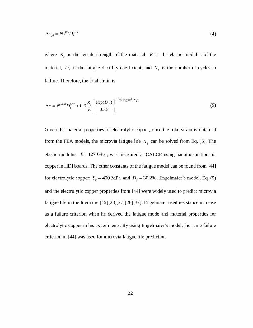
32
0.6 0.75
pl f fN D (4)
where uS is the tensile strength of the material, E is the elastic modulus of the
material, fD is the fatigue ductility coefficient, and fN is the number of cycles to
failure. Therefore, the total strain is
0.1785log(10 / )
0.6 0.75
5
exp( )0.9
0.36
N
fuf f
fDSN D
E
(5)
Given the material properties of electrolytic copper, once the total strain is obtained
from the FEA models, the microvia fatigue life fN can be solved from Eq. (5). The
elastic modulus, 127 GPaE , was measured at CALCE using nanoindentation for
copper in HDI boards. The other constants of the fatigue model can be found from [44]
for electrolytic copper: 400 MPauS and 30.2%fD . Engelmaier’s model, Eq. (5)
and the electrolytic copper properties from [44] were widely used to predict microvia
fatigue life in the literature [19][20][27][28][32]. Engelmaier used resistance increase
as a failure criterion when he derived the fatigue mode and material properties for
electrolytic copper in his experiments. By using Engelmaier’s model, the same failure
criterion in [44] was used for microvia fatigue life prediction.

33
Total Strain from FEA
To estimate the microvia fatigue life, the input to Eq. (5) is the total strain , which
is obtained from the FEA in this study. In order to minimize the element density effect
on the total strain, a group of elements at the neighborhood of the potential failure site
of the microvia was used to calculate the weighted average total strain:
e e
FEA e
V
V
(6)
where eV is the element volume, and
e is the element total strain. The element group
was selected as a circular slice (a quarter of a circle in the quarter model), taking about
1/8 of the single-level microvia height at the maximum von Mises stress location.
Application of Miner’s Rule
The damage from the sequential loading conditions accumulates for fatigue, according
to Miner’s Rule [45]:
1i
i i
n
N (7)
where in is the number of applied cycles and
iN is the limit number of cycles to failure
under loading i .
In this study, three solder reflow cycles were simulated and followed by thermal
cycling of −55 °C to +125 °C. The applied number of cycles to failure of the thermal

34
cycling was predicted. Based on FEA results, the total strain of the first solder reflow
cycle was much larger than that of the second and third solder reflow cycles due to
hardening of the copper structure. Therefore, the first solder reflow cycle was treated
as the first load, the second and third solder reflow cycles as the second load, and the
thermal cycling was the third load. In other words, 1 1n and
2 2n , and the aim is to
predict 3n .
The limit number of cycles to failure under each load was calculated using
Engelmaier’s fatigue life model, Eq. (5) based on the total strain from FEA, that is,
( 1,2,3)iN i was estimated. From Eq. (7), the applied number of thermal cycles
(−55 °C to +125 °C) to failure was derived as
3 3
1 2
1 21n N
N N
(8)
Parametric Study
A parametric study of void shape, size, and location, as well as microvia AR and
dielectric material properties, was conducted to investigate their effects on the thermo-
mechanical stress distribution and durability of microvias. Based on the examination
of the commercial HDI boards, four geometries were extracted from the void shape:
conical, spherical, cylindrical, and teardrop-shaped. The conical shape was the most
common void shape, representing more than half of the examined voids, followed by
the spherical shape.

35
The four different void shapes simulated in the microvias are shown in Figure 17. It
was assumed that the voids were located at the center of the stacked microvias. The
same void size was used to examine the microvia fatigue life for all the void shapes.
Whenever a void had a corner, where the radius of curvature had a sudden change, the
corner was smoothed using tangential surfaces to avoid artificial stress concentration.
The corners of the voids are marked in Figure 17.
Figure 17: Microvia Models of Different Void Shapes
The effect of different void sizes on microvia fatigue life was studied using both conical
and spherical voids. The void size was measured by volume ratio, which was defined
as the ratio of the void volume to the microvia volume. 4%, 8%, 12%, and 16% voids
were modeled for the two shapes.
To study the effect of void location, spherical voids of 12% were simulated at different
heights throughout the stacked microvia structure. Void locations were defined using
numerical data for generalizing the findings. The center of the middle-level microvia
is defined as Location 0, and half microvia height (single-level height) above Location
0 is defined as 0.5, half microvia height below Location 0 is defined as –0.5, and so on.
The location definitions are shown in Figure 18.
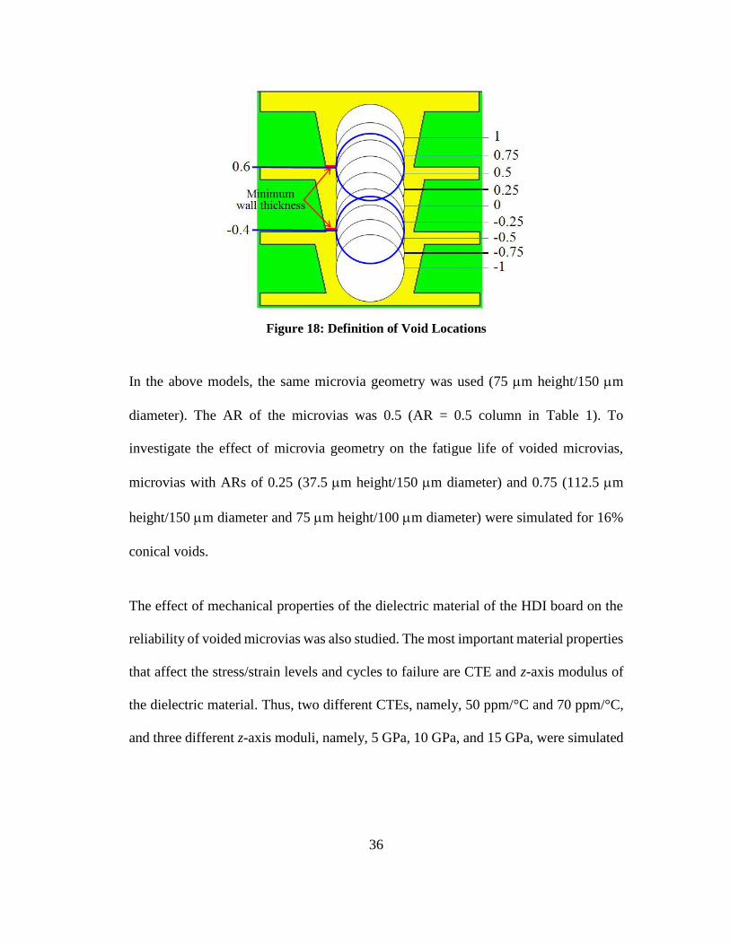
36
Figure 18: Definition of Void Locations
In the above models, the same microvia geometry was used (75 m height/150 m
diameter). The AR of the microvias was 0.5 (AR = 0.5 column in Table 1). To
investigate the effect of microvia geometry on the fatigue life of voided microvias,
microvias with ARs of 0.25 (37.5 m height/150 m diameter) and 0.75 (112.5 m
height/150 m diameter and 75 m height/100 m diameter) were simulated for 16%
conical voids.
The effect of mechanical properties of the dielectric material of the HDI board on the
reliability of voided microvias was also studied. The most important material properties
that affect the stress/strain levels and cycles to failure are CTE and z-axis modulus of
the dielectric material. Thus, two different CTEs, namely, 50 ppm/°C and 70 ppm/°C,
and three different z-axis moduli, namely, 5 GPa, 10 GPa, and 15 GPa, were simulated

37
in six microvia models (AR of 0.5 and 16% conical void). The other material properties
of these models were the same as in Table 2.
Results
The results of the parametric study of different void shapes, sizes, and locations, as well
as different microvia ARs and dielectric material properties, on microvia fatigue life
are presented in this section.
Void Size Effect
Figure 19 shows the cycles to failure of microvias with different spherical and conical
void sizes. For conical voids, the microvia fatigue life decreased as the void size
increased. The number of cycles to failure of a microvia with a 16% conical void was
only 5.4% of the cycles to failure of a non-voided microvia.
Figure 19: Effect of Void Size on Microvia Fatigue Life
For a spherical void, the microvia fatigue life first increased and then decreased as the
void size increased. When there is a void in the microvia structure, the stress and strain

38
distributions are different from the non-voided microvia, because the microvia
structure surrounding the void (referred to below as the “voided layer”) becomes more
compliant. For example, the strain increases in the voided layer, while it decreases in
the microvia structure above and below the voided layer. For a small void, the strain in
the voided layer is still smaller than in the microvia structure above or below the voided
layer, and therefore the strain level in the voided microvia is lower than a non-voided
microvia, which results in an increased fatigue life. A spherical void was beneficial up
to a certain void size (around 8%). When the void became larger than the cross-over
point, the thinner microvia wall generated by the void led to a lower fatigue life,
because the strain level in the voided layer exceeded that in the structure above or below
the voided layer. The fatigue life of a microvia with an 8% spherical void was 10%
longer than the fatigue life of a non-voided microvia, while the fatigue life of a microvia
with a 16% spherical void was 25% of the fatigue life of a non-voided microvia.
Void Shape Effect
Figure 20 presents the cycles to failure of microvias with four different void shapes of
the same size (12% volume ratio). The fatigue life of the microvia was highly
dependent on the void shape. The conical void resulted in the shortest fatigue life, while
the spherical void resulted in the longest fatigue life. The fatigue life of the conical void
was about 19% of that of the spherical void. The fatigue life of microvias with teardrop-
shaped and cylindrical voids was 63% and 60% of microvias with spherical voids,
respectively.

39
Figure 20: Effect of Void Shape on Microvia Fatigue Life
The longer fatigue life in the spherical void was due to the uniform radius of the void
boundary. The conical void had two corners (Figure 17), which resulted in the greatest
local stress concentration and hence the shortest fatigue life. A large region of the
teardrop-shaped void boundary had a uniform radius, and there was one corner on the
void boundary. In the cylindrical void, the lateral surface of the void boundary had
uniform curvature. Although the connection between the lateral surface and the base
surfaces formed two corners, the angles of the corners were 90° (not an acute angle).
Therefore, the teardrop-shaped and cylindrical voids resulted in longer fatigue life than
the conical void and shorter fatigue life than the spherical void.
Void Location Effect
Due to the tapered shape of microvias, void location change results in different
minimum wall thickness between the void boundary and the outside edge of the
microvia. Multiple void locations were simulated in each stack level to capture the
fatigue life change along with the changes in the microvia wall thickness. Apparently,
the voids located at 0.6 and -0.4 (Figure 18) resulted in the thinnest minimum wall. The

40
wall thickness at location 0.6 and -0.4 is about 5 m. It is thinner than the minimum
copper plating thickness in microvias required by IPC-6012D-RedLine [33]. However,
this does not affect our discussion on how microvia wall thickness affects the life time.
Moreover, the very thin plating wall was generated due to the specific void locations.
On other models in the dissertation, the void was located in the center of the microvia,
so other models did not have as thin as 5 m microvia walls.
Figure 21 shows the change of minimum wall thickness and cycles to failure of
microvias with the varying void location. The void at Locations -0.4 and 0.6 resulted
in the thinnest minimum microvia wall thickness and shortest fatigue life (local
minimum on the curve). However, the minimum wall thickness at different microvia
levels had different effects—for example, the local minimum fatigue life at location
0.6 was actually longer than the fatigue life at locations between -1 and 0 due to the
effects of the entire microvia geometry. The lower level minimum wall thickness
resulted in shorter microvia fatigue life than the same upper level minimum wall
thickness.

41
Figure 21: Effect of Void Location and Minimum Wall Thickness
The trend of cycles to failure was consistent with that of the minimum wall thickness,
except for location 1, which resulted in maximum stress at the top pad corner of the
microvia rather than around the minimum wall thickness site for other void locations.
The void location 1 was close to the top of the micoriva, so the stress distribution on
the microvia could be different than other locations. The shortest microvia fatigue life
at location -0.4 was 32% of the longest fatigue life at location 0.25.
Aspect Ratio Effect on Voided Microvias
The estimated cycles to failure of voided microvias with different ARs are presented in
Figure 22, which shows that smaller ARs are associated with longer microvia fatigue
life. The AR of 0.5 (75 m/150 m) was the default microvia geometry for the previous
models. The AR of 0.25 was achieved by reducing the dielectric thickness to half; the
AR of 0.75 was achieved in two ways—by increasing the dielectric thickness by half
or by reducing the microvia diameter by a third.

42
Figure 22: Effect of Microvia Aspect Ratio on Microvia Fatigue Life
The number of cycles to failure of the microvia (with 16% conical void) with AR of
0.25 was 36 times that of the microvia with AR of 0.5; the number of cycles to failure
of the microvia with AR of 0.5 was 7.5 and 12 times that of the microvias with AR of
0.75 for 112.5 m/150 m and 75 m/100 m geometry, respectively. Therefore, a
larger AR resulted in shorter microvia fatigue life, regardless of whether the AR was
generated by changing dielectric thickness or microvia diameter.
Interestingly, the fatigue life of the voided microvia of 0.25 AR was even longer than
that of a non-voided microvia of 0.5 AR—821,000 vs 415,000 cycles to failure.
Consequently, it is not sufficient to simply provide a qualification criterion for voided
microvias without considering the microvia geometries as in IPC-6012D-RedLine.
To better understand the effect of AR on the reliability of microvias containing conical
voids of varying sizes, microvias with an AR of 0.75 and with void size up to 16% were
modeled. As shown in Figure 23, the fatigue life of microvias of 0.75 AR had the same

43
trend as those with 0.5 AR—the fatigue life decreased as the conical void size
increased. The microvias of 0.75 AR always resulted in a shorter fatigue life than those
with 0.5 AR for the same void size. Moreover, voids had a more significant effect on
the fatigue life of microvias with a higher AR—the cycles to failure of the microvia of
0.75 AR with a 16% void was only 1.4% of that of the microvia without a void.
Figure 23: Effect of Microvia Aspect Ratio with Different Void Size
Material Property Effect on Voided Microvias
The effect of dielectric material properties on the fatigue life of voided microvias is
shown in Figure 24. A larger z-axis CTE or a larger elastic modulus resulted in a shorter
fatigue life. As the z-axis CTE increased by 40% (from 50 ppm/°C to 70 ppm/°C), the
fatigue life decreased by 95%, 92%, and 88% for a z-axis modulus of 5 GPa, 10 GPa,
and 15 GPa, respectively. As the modulus increased by 100% (from 5 GPa to 10 GPa),
the fatigue life decreased by 65% and 44%, respectively, for z-axis CTE of 50 ppm/°C
and 70 ppm/°C; as the modulus increased by 200% (from 5 GPa to 15 GPa), the fatigue
life decreased by 78% and 48%, respectively, for z-axis CTE of 50 ppm/°C and 70
ppm/°C. Therefore, the change of z-axis CTE had a more significant impact on

44
microvia fatigue life than elastic modulus. Additionally, the voided microvias with z-
axis CTE of 70 ppm/°C only lasted for about 1000 cycles under the thermal loading
condition.
Figure 24: Effect of Dielectric Material Properties
Potential Failure Sites
The site of the maximum von Mises stress is a potential site for maximum damage and,
hence, is a potential fatigue failure site in a microvia. Therefore, the identification of
the site is helpful for microvia reliability evaluation and improvement.
As shown in Figure 25, for a non-voided microvia, the site of maximum von Mises
stress was at the top and/or bottom pad corner of the microvia due to CTE mismatch in
the board thickness direction between the copper material and the dielectric. For conical
voids, the maximum von Mises stress was located at the void boundary or microvia
outside wall with minimum microvia wall thickness, due to local stress concentration.
For spherical voids, when the voids were equal to or less than 8% volume ratio (default

45
microvia AR and dielectric material properties), the potential site of maximum damage
was the same as in non-voided microvias; the major effect of the void was the change
of the compliance of the microvia structure, which resulted in an increase in microvia
fatigue life. When the spherical void reached 12% or larger, the thin microvia wall
generated a greater stress concentration than at the top or bottom pad corner, and the
maximum von Mises stress was located at the void boundary with a larger stress level
than the non-voided microvia.
Figure 25: Sites of Maximum von Mises Stress
Discussion about the Voiding Effects
Although voids have been observed in copper-filled microvias, their existence is not
always detrimental to microvia reliability. For example, 8% or smaller spherical voids
resulted in longer fatigue life than microvias without voids, while larger voids resulted
in shorter fatigue life than non-voided microvias. The voided layer in a microvia can
be considered as a composite of the copper and the void. In the simplest case of
effective material properties (Rule of Mixtures), each component (i.e., copper and void)
contributes to the effective modulus in a quantity proportional to its volume fraction.
The modulus of the void is considered as zero, and therefore, the effective modulus of

46
the voided layer decreases (or in other words, the compliance of the voided layer
increases). As confirmation of this, the FEA results show that for microvias with
spherical voids, the average strain in the voided layer increased with increasing void
size, while the average strain in the microvia structure above and below the voided
layer decreased. When the spherical void was smaller than the cross-over size of around
8%, the strain level in the voided layer was still lower than the microvia structure above
or below the voided layer, which was smaller than the strain level of the non-voided
microvia. Thus, the small spherical void resulted in more cycles to failure than the non-
voided microvia. When the spherical void was larger than the cross-over size, the strain
level in the voided layer exceeded that in the microvia structure above or below the
voided layer, and consequently, the microvia fatigue life started to decrease. The
increase of fatigue life due to small spherical voids was also seen from voided solder
balls [46]. On the other hand, conical voids greatly decreased the thermo-mechanical
reliability of microvias, regardless of the void size, because the strain in the voided
layer was much greater than in the microvia structure above and below the voided layer
even for small voids. For example, a conical void as small as 4% resulted in a 38%
drop in the microvia fatigue life.
This study demonstrated that the microvia AR and z-axis CTE of the dielectric material
had a significant impact on the fatigue life of voided microvias. A larger AR resulted
in a shorter fatigue life; a larger z-axis CTE resulted in fewer cycles to failure.
Experimental studies from the literature can provide support for this finding. Though

47
voiding was not concerned, Lesniewski [12] tested microvias with ARs of 1 and 0.5
fabricated with dielectric materials A, B, and C having z-axis CTEs of 70, 55, and 35–
45 ppm/°C, respectively. Under the same thermal loading condition, microvias with
material A always failed earlier than B and C, and microvias with material C
experienced the most cycles prior to failure. For another thermal loading condition,
failure was observed on microvias of AR of 1 within 1000 cycles, while all microvias
of AR of 0.5 survived after 1500 cycles of testing.
Moreover, as the diameter of the microvias gets smaller and smaller for denser I/O
applications today, voiding defects become more of a problem for reliability. For
example, the voided microvia with default microvia geometry (AR of 0.5) can have up
to 510 cycles to failure, which is normally not a concern for reliability (2000 cycles to
failure under the −55 °C to +125 °C thermal cycling is usually used as a qualification
criterion in the industry). However, with the AR of 0.75, the fatigue life of the voided
microvias was as low as about 1674 cycles, and obviously, the reliability is not
acceptable.
Additionally, the stress/strain distributions of TSVs and microvias were compared to
explore the differences in the two copper-filled interconnection structures. To make the
same baseline for comparison, the authors first duplicated a TSV model from Liu et al.
[37]. Using the same geometry, material properties, and loading condition as in [37],
the authors obtained stress/strain results very close to those in [37] for the non-voided
TSV with an AR of 2. The maximum first principle stress at 125 °C in the dielectric is

48
176.3 MPa from the authors’ simulation and 177 MPa from [37]—resulting in a
difference of 0.4%. The authors generated a maximum equivalent plastic strain of
1.35e-3, about 5.8% smaller than the result from [37]. The close results between the
authors’ TSV models and the TSV models from [37] verified that the authors FEA
modeling is equivalent to the modeling in [37]. However, the differences in dielectric
material properties between microvias and TSVs resulted in about an order of
magnitude smaller plastic strain (i.e., 2.93e-4) in a microvia with total AR of 2.05 (the
AR of each microvia level is 0.5). When voids of the same volume ratio were present
in the TSV and microvia at the same location, they resulted in not only different strain
levels, but also different maximum strain sites, as shown in Figure 26. Therefore,
thermo-mechanical reliability studies require the creation of TSV and microvia models
separately, and one cannot derive the reliability of one via type from the other.
a) TSV with a 12% void (b) Microvia with a 12% void
Figure 26: Maximum Strain Sites in TSV and Microvia

49
Microvia Virtual Qualification
According to the analysis above, the reliability of microvias is affected by many factors,
such as microvia geometry, material properties, and defect characteristics (e.g., void
shape, size, and location). The design parameters and defect variables affect microvia
fatigue life in different ways. However, it is extremely time-consuming and costly to
test all the potential microvia designs and defect variables to determine optimal or
acceptable HDI board designs or production processes. A fast and inexpensive method
is desirable for microvia design and process qualification. A microvia virtual
qualification (VQ) method for HDI boards using FEA and fatigue life prediction can
serve this purpose.
The microvia VQ method is shown in Figure 27. This method can be used to verify
microvia designs prior to HDI fabrication (Figure 27 (a)), or used for process
qualification and improvement during HDI production (Figure 27 (b)). For both
applications, the VQ method reduces or eliminates the need for multiple “design-build-
test-improve” cycles.
(a) Virtual qualification of design

50
(b) Virtual qualification of process
Figure 27: Microvia Virtual Qualification Method
The VQ of microvia designs (as shown in Figure 27 (a)) is mainly used to verify the
material selection and microvia geometry. With the expected life cycle load or
accelerated testing load, as well as potential defect characteristics (obtained by 2D X-
ray inspection of HDI boards and optical microscopy on microvia cross-sections) based
on process capability, FEA models are built to access the stress/strain distribution of
the microvia design. Then the microvia fatigue life can be predicted with the total strain
obtained from the FEA. Finally, a decision is made on whether the fatigue life is
sufficient based on the application of the HDI board. If not, the design is revised to
improve the fatigue life, and the new design goes through VQ again.
The VQ of the microvia production process starts with process characterization and
evaluation of microvia defects (using 2D X-ray inspection of HDI boards and optical
microscopy on microvia cross-sections). With the defect characteristics associated with
the process, FEA models are built for the specific microvia geometry and material
properties. Life cycle load or accelerated testing load profiles are applied to the finite

51
element models to solve the stress/strain distribution of the microvia structures. The
fatigue life of the microvia is predicted using a fatigue life model with the total strain
obtained from FEA. Similar to the virtual design qualification, a decision is made on
whether the microvia fatigue life is sufficient. If not, the process is revised to mitigate
the defects.
In cases where there is little prior experience with a microvia design or process, or
when boards will be used in a high-reliability application, then the VQ described above
can be supplemented by testing to validate the predictions of fatigue life. Even in those
cases VQ can reduce the amount of testing needed to arrive at an acceptable design or
process, employing VQ as a parameter screening step. One way of using VQ for this
purpose is to narrow the range of acceptable design or process parameters prior to
testing. The designs or defects that lead to insufficient fatigue life can be identified,
allowing reliability tests to focus on the parameter values most likely to satisfy
reliability requirements for the product. Another way in which VQ can serve as a
parameter screening tool is by identifying those parameters that have the most influence
on fatigue life. For example, it is possible that the three board materials under
consideration are all predicted to give approximately the same fatigue life, in which
case dielectric material could be excluded as a parameter for testing and reliability
testing could focus on the most critical parameters rather than on all the possible design
or process variables. In this manner, significant testing time and cost can be saved.

52
The microvia VQ method developed in this study is intended for use with bare HDI
printed circuit boards. It does not specifically address applications involving HDI
substrates in packaged devices, though it may be possible to extend it to such
applications if the finite element models are developed for such applications with the
appropriate boundary conditions. By modeling microvias in a package or in a PCB
assembly, microvia fatigue life in the specific context can be predicted.
In addition, the VQ method developed in this study focuses on qualifying and verifying
HDI board design and process capability. When it comes to the production consistence
and supplier monitoring, on-going reliability test (ORT) can be used to evaluate and
verify the product quality and reliability from mass production.
Voided Microvias Acceptance Criterion
IPC-6012D-RedLine defines the voided microvias acceptance criterion as that the void
should not exceeds 25% of the area of the filled microvia in the center cross-sectional
plane. However, this criterion is not appreciate for stacked microvias. The researcher
simulated single-level, 3-level, and 5-level microvias to investigate the proper criteria
for different microvia stack levels. In the simulation models, worst scenarios were
used—the conical shape, the largest z-axis CTE of the dielectric material, and the
largest allowed microvia AR that can maintain an acceptable yield.
2000 cycles to failure are commonly used in the electronics industry to determine if
microvias pass the qualification test (−55 °C to +125 °C cyclic thermal loading) [16]-

53
[20]. Using 2000 cycles to failure as the criterion, the researcher’s modeling results
show that the acceptance criterion should be no greater than 14% area ratio for 3-level
stacked microvias, and no greater than 9% area ratio for 5-level stacked microvias.
However, for single-level microvias, the fatigue life is above 25,000 cycles to failure
when the void area ratio is 25%. If the void size is larger than 25%, the void boarder
will become thinner than 8 m. In the perspective that the void boarder should not be
too thin (for example, IPC-6012D-RedLine [33] requires minimum copper plating
thickness as 10 m), 25% criterion for single level microvia makes sense. The
simulation results are in Figure 28, Figure 29, and Figure 30.
Figure 28: Cycles to Failure vs. Void Area Ratio for 3-Level Stacked Microvias

54
Figure 29: Cycles to Failure vs. Void Area Ratio for 5-Level Stacked Microvias
Figure 30: Cycles to Failure vs. Void Area Ratio for Single-Level Microvias
Summary
This study investigated the effects of voids on thermo-mechanical reliability of copper-
filled stacked microvias. A parametric study of microvias with various voiding
characteristics under thermal cycling demonstrated that different void shapes, sizes,

55
and locations, as well as different microvia ARs and dielectric material properties, led
to different cycles to failure. The conclusions of this study are especially useful for the
development of acceptability standards for HDI boards, for board manufacturers to set
their process targets, and for OEMs who regularly conduct cross-sections and 2D (and
3D) X-ray inspections to evaluate the board quality. Note that the quantitative results
of this study were based on three-level stacked microvias.
Large voids decrease the thermo-mechanical reliability of microvias due to local stress
concentration, while small spherical voids may actually result in longer fatigue life due
to increased compliance and strain redistribution. The cross-over void size above which
a void decreases the microvia fatigue life is determined by the microvia geometry (e.g.,
AR) and dielectric material properties. When a void is larger than the cross-over size,
it is referred as a “large void”; otherwise it is referred to as a “small void” in this study.
According to the authors’ investigation of production HDI boards, conical voids are the
most common voiding geometry, and they are also the worst void shape with respect
to fatigue life. For instance, a 16% conical void can reduce microvia fatigue life by
98.6%. Changing the void location affects the minimum microvia wall thickness,
which, together with the stack level where the void is located, governs the stress/strain
distribution in microvias.
Among all the parameters studied in this paper, microvia AR and z-axis CTE of the
dielectric materials have the strongest influence on the lifetime of microvias. Therefore,
these two parameters should be given the most attention for HDI board design and

56
experimental testing. As for different voiding characteristics of a particular board
design, more attention should be paid to the most critical void shape and location—a
conical void with the thinnest minimum microvia wall thickness—for which the larger
the void size, the less reliable the microvia.
Though the microvia fatigue life varies from board to board, this study has identified
the following general trends: (1) conical voids result in greater decrease in microvia
fatigue life than other void shapes; (2) large voids can reduce microvia fatigue life
greatly, while small spherical voids can actually increase the cycles to failure; (3) large
voids associated with thinner microvia walls result in shorter fatigue life in the same
stack level; (4) smaller microvia AR results in longer fatigue life; and (5) smaller CTE
or modulus of the dielectric material results in longer fatigue life.
A microvia VQ method has been proposed for design and process qualification to
reduce the need for multiple “design-build-test-improve” cycles. Even when VQ is
paired with some amount of reliability testing, it can be used as a parameter screening
method, to identify the acceptable ranges of design or process parameters or to
determine the most critical design parameters and process variables. In this manner,
VQ can help to decrease HDI board development time and cost.
According to this study, the criterion (25% area ratio) for voided microvia qualification
in the IPC-6012D-RedLine are not appropriate for stacked microvias. Considering the
worst scenario, this study has determined that the void acceptance criterion should be

57
no great than 14% area ratio for 3-level stacked microvias, and no greater than 9% area
ratio for 5-level stacked microvias.

58
Development of a Regression Microvia Strain Life
Model Using Response Surface Method
This study aims to develop a second-order regression strain life prediction model for
copper-filled stacked microvias that accounts for the nonlinear relationship between
the fatigue life and the microvia parameters. A DOE was conducted with microvia
design parameters, material properties, as well as a voiding defect variable. The design
parameters included microvia diameter and dielectric thickness. The materials used for
the DOE represent the currently commonly used materials and the state of the art for
next-generation materials. For the defect variable, different void sizes were simulated
in microvias. Finite element models were created with varying microvia parameters
(factors). The total strain, which is used for microvia fatigue life calculation, was
determined from the FEA. The response surface method (RSM) was used to develop a
regression model between the total strain and the microvia parameters. Then the
developed regression model together with the combined Basquin and Coffin–Manson
fatigue model was used to predict the fatigue life of microvias due to thermal loading.
The Basquin and Coffin–Manson fatigue model, Eq. (5) and the electrolytic copper
properties are introduced in Section 3.2.1, Chapter 3.
Design of Experiments
To develop the regression model for predicting the total strain, it is critical to select
control variables that are most responsible for the thermo-mechanical fatigue failure.

59
The factors that may influence microvia fatigue life can be categorized into three
groups: geometric design, material properties, and process parameters. This section
presents the selection of microvia parameters and the DOE for RSM regression.
Control Variables from Geometric Design
The essential geometric parameters of microvias include dielectric thickness (also
known as microvia height), microvia diameter (dielectric thickness and microvia
diameter together determine another crucial parameter, the AR of the microvia, which
is the dielectric thickness over the microvia diameter), and microvia stack levels. This
study focuses on three-level stacked microvias, which are commonly used in current
and anticipated future HDI designs [3]. Dielectric thickness and microvia diameter
were selected as factors in the DOE.
The largest microvia diameter based on the definition of microvia is 150 µm. According
to HDI industry experts and iNEMI Technology Roadmaps [3], in current practice, the
lower limit on microvia diameter is 75 µm for consumer electronics and 100 µm for
military applications. Considering technology advances in the future, a reasonable
range for microvia diameter is 50 µm to 150 µm in the DOE.
The lower limit for dielectric thickness is controlled by the amount of crosstalk between
conductor layers in a board; board layers no thinner than 25 µm are usually used for
this reason. Dielectric thicknesses of up to 75 µm were observed from production HDI
boards. Therefore, a dielectric thickness range of 25 µm to 75 µm is selected.
60
The ranges of microvia diameter and dielectric thickness result in a microvia AR from
0.17 to 1.5, which is more than enough to cover the commonly used AR—no larger
than 0.8 (a larger AR usually leads to unacceptably lower yield).
Control Variables from Material Properties
Microvia fatigue failure occurs because of CTE mismatch in the out-of-plane direction
of the HDI board (z-axis). Therefore, the most important material properties that affect
the cycles-to-failure include z-axis CTE and z-axis modulus.
Dielectric materials in current use (e.g., EM-827, EM-828G, Isola 370HR, and Megtron
6) and future generation materials for HDI design (e.g., Megtron 7 and Tachyon) have
glass transition temperatures, 𝑇g, between 160 °C to 210 °C, which is higher than the
thermal loading condition (-55 °C to 125 °C) discussed in this study. Hence, this study
uses material properties below 𝑇g.
The z-axis CTE range (below 𝑇g) of the commonly used HDI materials and future
generation materials is 42 to 50 ppm/ºC according to the material data sheets. Materials
with z-axis CTE of 35 to 70 ppm/°C were used in reliability tests of microvias in the
literature [12]. To cover most dielectric materials, the z-axis CTE range of 35 to 70
ppm/°C is used in the DOE. The z-axis CTE range in this study covers FR4 type of
HDI materials, some ceramic-filled high frequency laminates are not in the scope of
this study. A range of z-axis modulus (below 𝑇g) of glass-fabric-composite substrates

61
from 3 GPa to 11 GPa is used in this study based on values reported in the literature
[31][40][43][47].
Control Variables from Manufacturing Process
Because of the inherent difficulty of quantifying the effect of process parameters, such
as copper plating time and current, on microvia reliability, parameters associated with
defects induced from the manufacturing process are considered in the DOE. Two
common defects, voiding generated from the copper plating process and via-to-via
misalignment in stacked structures, are investigated in this study.
In the parametric study, the authors have found that conical voids located at the center
of microvias have a more significant effect than other void types in reducing microvia
fatigue life; larger voids resulted in less cycles to failure. Therefore, conical voids at
the microvia center were simulated in this study, and the void size is used as a factor in
the DOE.
To examine how microvia misalignment affects microvia fatigue life, FEA models with
different misalignment ratios (MRs) were simulated. MR is defined as the ratio of the
offset of the axes of two neighboring microvias in a stack to the radius of the microvias
( ro / as illustrated in Figure 31). The FEA modeling results for models with MRs of 0,
0.5, 1, and 2 are shown in Table 3. When MR was no greater than 1, the difference in
total strain was negligible, while an MR of 2 resulted in a much higher total strain.
Figure 32 shows that the maximum stress was located at the bottom corner for

62
microvias with MR of 0 and 0.5, at the middle-level microvia wall for MR of 1, and at
the corner formed by misalignment for MR of 2.
Figure 31: Definition of MR (MR =o/r )
Table 3: Total Strains of Microvias with Different MRs
MR 0 0.5 1 2
Total Strain 0.00280 0.00278 0.00268 0.00577

63
Figure 32: Stress Distributions of Microvias with Different MRs
According to IPC-6016 [48], for laser-drilled microvias, the microvia and
capture/target pad should have tangency at a minimum; breakout (resulting in reduced
contact area between the microvia and the capture/target pad) is not allowed. Though
the criterion was formulated for via-to-pad misalignment in single-level microvias, the
same threshold can be considered for via-to-via misalignment—a microvia with MR
no greater than 1 is acceptable (no breakout), but a microvia with MR larger than 1 can
result in breakout, which is not allowed. Therefore, only MR values between 0 and 1
are considered for this study. However, due to the negligible difference between the

64
total strains for microvias with MR between 0 and 1, misalignment was not selected as
a factor in the DOE.
Box-Behnken Design
In this study, the experiments are numerical simulations of microvias using FEA, and
therefore, there is only one replicate per run of the experiments. RSM is used to
formulate the regression model. To capture the nonlinear relationship between the total
strain and the microvia design, material, and defect parameters, a quadratic model
(second-order model) is used for regression:
2
0
1 1
k k
i i ij i j ii i
i ii j
y x x x x
(9)
where y is the response (total strain) and ( 1,2, )ix i k represents a number of factors
(i.e., dielectric thickness, microvia diameter, z-axis CTE, z-axis modulus, and void size
in this study). k is the number of factors, and 5k for this study. indicates the error
of this model.
To capture the quadratic relationship between the response and the control factors, the
experiments must involve at least three levels for each factor. A 3k full factorial design
consists of all the combinations of the k control factors, which have three levels each.
However, when 5k , 243 experiments would be required. As a more efficient
alternative, in engineering research, Box–Behnken designs [49] are widely used for
RSM.

65
Box–Behnken designs require three levels for each factor where the settings are –1, 0,
and 1. The Box–Behnken design with 5 factors requires at least 41 experiments
including 1 center point in the design space. The 41 experiments for this study are listed
in Table A.I in Appendices. The three levels of the control factors are selected to
represent current and state-of-the-art HDI technologies. Table 4 lists the values of the
three levels of each factor.
Table 4: Three Levels of the Factors
Level Dielectric
thickness (µm)
Microvia
diameter (µm)
z-axis CTE
(ppm/°C)
z-axis modulus
(GPa)
Void size
(%)
–1 25 50 35 3 0
0 50 100 52.5 7 8
1 75 150 70 11 16
Finite Element Modeling and Results
The experiments in this study were finite element simulations of microvias with
different design, material, and defect parameters as shown in Table 4. 3D FEA was
used to study the relationship between the total strain and the microvia parameters. As
mentioned in Section 4.1.1, this study focused on three-level stacked microvias.
[3+4+3]-layer HDI boards with different parameters were simulated. Due to differences
in boundary conditions and qualification requirements between HDI bare board and
HDI substrates within packaged components, the scope of this study has been limited
to modeling and predicting fatigue life of microvias in bare HDI boards. When
components are assembled to the bare circuit board, the boundary conditions,
compliance of the entire board, and the stress state of microvias may be changed.

66
Therefore, the predicted microvia fatigue life from the model in this study cannot be
directly used in HDI assemblies, either. However, the relative bare board microvia life
with vs. without voiding is relevant to HDI assemblies and HDI substrates within
packaged components. According to the study, large voids result in shorter microvia
life in the bare HDI board. Similarly, Wang, et al. [30] found that a hollow microvia
had a much shorter fatigue life than a fully filled microvia in a PCB assembly; Wang
and Lai [29] found that unfilled microvia had a higher stress than a filled microvia in
an MCM package.
The following additional considerations and assumptions are made for this study:
1) Two materials, FR4 type of glass-reinforced dielectric and electrolytic copper, are
simulated in the finite element models. Electroless copper and board finishing
layers (e.g. solder mask) are used in the HDI fabrication process, but they are not
considered in the models because of their small volume and negligible effect to the
FEA results. For example, the thickness of electroless copper is only 0.5 – 3 µm [2]
compared to the microvia height of 37.5 – 75 µm in different microvia models; the
material properties of electroless copper were considered the same as electrolytic
copper in the finite element models. Solder mask does not only have a negligible
volume, but its elastic modulus (2.4 – 3.2 GPa) [29], [31] is also negligible
compared to the modulus of copper (127 GPa, as measured in the Authors’ lab).
2) All the microvias are filled with electrolytic copper (some have voids in the

67
electrolytic copper structure).
3) The stacked microvias are perfectly aligned between different levels. Although via-
to-via misalignment may occur in practice, the effect of misalignment on the total
strain of microvias is not significant (when the MR is no larger than 1) according
to the modeling results in Section 4.1.3. Therefore, microvia misalignment was not
considered in the DOE.
4) Since the simulated thermal load is below the glass transition temperature of the
dielectric materials, the creep of the dielectric materials is negligible.
Finite Element Models
The finite element models are unit cells that simulate the thermo-mechanical behaviors
of microvias. The microvia unit cell was introduced in Section 3.1.1, Chapter 3. Proper
periodic BCs were applied on the microvia unit cell to ensure compatibility with
adjacent microvias around the unit cell and the rest of the HDI board. A quarter model
was used due to symmetry of the unit cell, and only the top half of the HDI board was
modeled due to symmetry with respect to the board mid-plane. Figure 33 shows a 3D
quarter model with meshing for a voided microvia used in this study. The number of
divisions of each line of the solid model was specified for meshing. The meshing on
and around the microvia was finer, and the meshing far away from the microvia was
coarser. The meshing of different microvia models had the same refined level for
different voiding conditions, which made the models comparable.

68
Figure 33: Voided Microvia Finite Element Model with BCs
Material Properties
Electrolytic copper is used for the conductor layers and microvia structures in the HDI
boards. The material properties of electrolytic copper can be found from Section 3.1.2,
Chapter 3.
Section 3.1.2, Chapter 3 also listed the orthotropic material properties of the dielectric
for the HDI board the researcher investigated. In this section, the material properties of
the dielectric material is general for the currently commonly used materials and the
state of the art for next-generation materials according to the analysis in Section 4.1.2.
The dielectric material properties for the microvia life modeling are shown in Table 5.
As discussed in Section 4.1.4, three levels of the z-axis CTE and three levels of the z-
axis modulus were used in the finite element models.

69
Table 5: Dielectric Material Properties
Temp (°C) Below 𝑇g
𝐸𝑥 (GPa) 20
𝐸𝑦 (GPa) 20
𝐸𝑧 (GPa) 3 7 11
𝐺𝑥𝑦 (GPa) 15
𝐺𝑦𝑧 (GPa) 2.4
𝐺𝑥𝑧 (GPa) 2.4
ν𝑥𝑦 0.13
ν𝑦𝑧 0.42
ν𝑥𝑧 0.42
α𝑥 (10–6/°C) 16
α𝑦 (10–6/°C) 16
α𝑧 (10–6/°C) 35 52.5 70
Total Strain from the FEA Experiments
A cyclic thermal load between −55 °C and +125 °C was simulated on the microvia
models. Under the thermal loading, the microvia experienced cyclic tensile and
compressive stresses and strains due to CTE mismatch between the dielectric material
and copper. In this study, the total strain generated per load cycle was used to predict
the cycles-to-failure. The total strain is calculated from the finite element models as
weighted average total strain using Eq. (6) in Section 3.2.2, Chapter 3.
The 41 experiments (finite element models) as shown in Table A.I and Table A.II in
Appendices were conducted to capture the relationship between the total strain and the
five microvia parameters. The total strain results are shown in Table A.II. For
convenience, in Table A.II and the following sections and chapters of this dissertation,

70
T, D, A, E, and V stand for the five factors—dielectric thickness, microvia diameter, z-
axis CTE, z-axis modulus, and void size, respectively.
Regression Analysis using Response Surface Method
With the experiment (simulation) results in Table A.II in Appendices, the response
surface regression analysis of a second-order model was performed using the R
package, rsm [50]. By fitting a second-order response surface model to the data, the
result is shown in Table 6. x1, x2, x3, x4, and x5 are coded variables, where x1 = (T -
50)/25, x2 = (D - 100)/50, x3 = (A - 52.5)/17.5, x4 = (E - 7)/4, and x5 = (V - 8)/8. 𝑅2 of
the fitted model is 96.1%, and adjusted 𝑅2 is 92.2%. The small p-values (a significance
level of 0.05 is usually used as a threshold) for linear, interaction and square terms in
Table 7 indicate that their contributions are significant to the model. (Some of the
individual terms have p-values larger than 0.05 in Table 6. Second-order models with
those terms removed are discussed in Section 4.4.)

71
Table 6: Response Surface Result with Coded Variables
Estimate Std. Error t value Pr(>|t|)
(Intercept) 2.78E-03 6.24E-04 4.4475 0.000247
x1 1.28E-03 1.56E-04 8.192 8.06E-08
x2 –1.94E-03 1.56E-04 –12.4104 7.49E-11
x3 1.90E-03 1.56E-04 12.185 1.04E-10
x4 6.83E-04 1.56E-04 4.3798 0.00029
x5 5.53E-04 1.56E-04 3.546 0.002027
x1:x2 –1.15E-03 3.12E-04 –3.6828 0.001475
x1:x3 7.99E-04 3.12E-04 2.5596 0.018689
x1:x4 2.39E-04 3.12E-04 0.7645 0.453524
x1:x5 1.92E-04 3.12E-04 0.6149 0.545568
x2:x3 –1.52E-03 3.12E-04 –4.8753 9.16E-05
x2:x4 –1.61E-04 3.12E-04 –0.5162 0.611362
x2:x5 –9.21E-04 3.12E-04 –2.952 0.007882
x3:x4 4.89E-04 3.12E-04 1.5661 0.133011
x3:x5 3.58E-04 3.12E-04 1.1483 0.264402
x4:x5 9.38E-05 3.12E-04 0.3007 0.766765
x1^2 7.24E-05 3.55E-04 0.2041 0.840333
x2^2 1.14E-03 3.55E-04 3.2232 0.004264
x3^2 2.98E-04 3.55E-04 0.8389 0.411448
x4^2 –1.84E-04 3.55E-04 –0.5187 0.609683
x5^2 –2.33E-05 3.55E-04 –0.0657 0.948258
Table 7: Analysis of Variance Table
Df Sum Sq Mean Sq F value Pr(>F)
Linear 5 1.56E-04 3.13E-05 80.2718 1.54E-12
Interaction 10 2.25E-05 2.25E-06 5.7687 0.000443
Square 5 1.34E-05 2.68E-06 6.8767 0.000698
Residuals 20 7.79E-06 3.90E-07
Lack of fit 20 7.79E-06 3.90E-07
Pure error 0 0.00E+00

72
Decoding the variables to the original units, the regression equation of the microvia life
model is:
6
2
2 2
10 ( 2723 11.27 31.14 19.88 96.93
102.4 0.9195 1.826 2.386
0.9594 1.739 0.8055 2.303
6.982 2.560 2.932 0.1158
0.4573 0.9715 11.50
T D A E
V TD TA TE
TV DA DE DV
AE AV EV T
D A E
2 20.3642 )V
(10)
A comparison of the strains obtained from the experiments (FEA models) and the
strains predicted with the regression model, Eq. (10) is shown in Figure 34. If the
regression model had predicted perfectly the strains from the FEA, the results would
lie along the theoretical line, representing a perfect fit. If a data point lies below the
line, the regression model under-predicted the strain value; if a data point lies above
the line, it corresponds to an over-prediction. Figure 34 shows that the predicted total
strains of the RSM regression model are close to FEA total strains.

73
Figure 34: Regression Model Predicted Strain vs. FEA Strain
The fatigue life of the microvia can be solved using the regression model predicted
total strain as an input to the electrolytic copper fatigue life model in Eq. (5). Figure 35
shows a log-log plot of the regression model predicted fatigue life compared to the life
estimated from FEA strain.
Figure 35: Log-Log Plot of Cycles-to-Failure: Regression Fit vs FEA

74
Discussion and Model Validation
In this section, the second-order regression model was simplified by removing those
terms that do not make significant contribution to the response (total strain). A
nonlinearity analysis was conducted by comparing the second-order model with first
order models. Then, the application range of the model was discussed. Finally, the
regression model was validated with extra data.
Model Simplification Using Least Square
In Table 6, the p-values of Terms x1x4, x1x5, x2x4, x3x4, x3x5, x4x5, x12, x32, x42, and
x52 are larger than the significance level of 0.05, and therefore these terms and their
decoded terms (TE, TV, DE, AE, AV, EV, 𝑇2, 𝐴2, 𝐸2, 𝑉2) are not significant. These
terms were removed from the model and a least square regression was performed to
generate a simplified model with the other linear, interaction, and square terms. The
summary of the least square model is shown in Table 8. R-squired of the model is
94.4%, and adjusted 𝑅2 is 92.5%. The linear terms T and D have larger than 0.05 p-
values in the least square model. These two terms were further removed, and a second
round of least square regression was conducted.

75
Table 8: Round 1 Least Square Simplification
Estimate Std. Error t value Pr(>|t|)
(Intercept) -9.64E-03 3.10E-03 -3.107 0.004114
T 4.72E-05 4.46E-05 1.06 0.297711
D 2.85E-05 2.79E-05 1.02 0.315711
A 1.91E-04 5.02E-05 3.807 0.000647
E 1.71E-04 3.83E-05 4.466 0.000105
V 3.00E-04 7.89E-05 3.797 0.000664
TD -9.20E-07 2.45E-07 -3.755 0.000744
TA 1.83E-06 7.00E-07 2.61 0.013991
DA -1.74E-06 3.50E-07 -4.971 2.53E-05
DV -2.30E-06 7.65E-07 -3.01 0.005253
DD 4.42E-07 7.84E-08 5.643 3.80E-06
Table 9 shows the Round 2 least square result. All the remaining terms in the model
are significant according to the p-values. 𝑅2 of this model is 94.1%, and adjusted 𝑅2 is
92.6%. The final regression model to predict total strain of microvias is:
6
2
10 5835 147 6 170 9 285 9 0 716
2 324 1 552 2 167 0 4781
(- + . A+ . E+ . V - . TD
+ . TA- . DA- . DV + . D )
(11)
Table 9: Round 2 Least Square Simplification
Estimate Std. Error t value Pr(>|t|)
(Intercept) -5.84E-03 1.14E-03 -5.098 1.49E-05
A 1.48E-04 3.75E-05 3.936 0.000419
E 1.71E-04 3.81E-05 4.484 8.84E-05
V 2.86E-04 7.66E-05 3.73 0.000743
TD -7.16E-07 1.89E-07 -3.795 0.000621
TA 2.32E-06 3.68E-07 6.316 4.36E-07
DA -1.55E-06 2.56E-07 -6.058 9.18E-07
DV -2.17E-06 7.42E-07 -2.919 0.006381
DD 4.78E-07 6.37E-08 7.507 1.51E-08

76
A comparison of the totals strain obtained from the FEA experiments and predicted
from the final second-order regression model, Eq. (11) is shown in Figure 36. The
microvia fatigue life using the regression model predicted strains against using FEA
strains is plotted with a log-log scale in Figure 37.
Figure 36: Predicted Strain vs. FEA Strain
Figure 37: Log-log Plot of Cycles-to-Failure: Final Regression Model vs. FEA

77
Nonlinearity Analysis
According to the 𝑅2 values, the second-order model, Eq. (11) is a very accurate fit of
the relationship between the total strain and the microvia parameters. The authors
further conducted a nonlinearity analysis to investigate how much improvement the
second-order model has made as opposed to first-order models (without or with
interaction terms) in predicting the total strain. The experiments (simulations) in Table
10 and Table 11 were used to generate the first-order models through least square
regression.
Table 10: First-Order Model with No Interactions
Estimate Std. Error t value Pr(>|t|)
(Intercept) -2.30E-03 1.31E-03 -1.75 0.0886
T 5.11E-05 1.16E-05 4.403 9.17E-05
D -3.87E-05 5.81E-06 -6.67 8.94E-08
A 1.09E-04 1.66E-05 6.548 1.29E-07
E 1.71E-04 7.26E-05 2.354 0.0242
Table 11: First-Order Model with Pairwise Interactions
Estimate Std. Error t value Pr(>|t|)
(Intercept) 7.16E-03 7.53E-04 9.502 1.81E-11
D -1.08E-04 1.45E-05 -7.482 6.52E-09
TD 4.27E-07 1.40E-07 3.061 0.00409
DA 9.20E-07 1.99E-07 4.617 4.58E-05
The result of the first-order model with no interaction terms is shown in Table 10. The
parameter, V was removed, because it was not significant to the total strain (the p-value
was larger than 0.05). The 𝑅2 of this model is 75.7%. Therefore, the first-order model

78
with no interaction terms is much less accurate than the second-order model, Eq. (11),
𝑅2 of which is 94.1%.
With pairwise interactions added to the first-order model, 𝑅2 is 61.7%, much smaller
than 94.1% of the second-order model, Eq. (11). Table 11 shows the model results after
the removal of non-significant terms with p-vales larger than 0.05. Only three terms,
D, TD, and DA are significant to the response in this model.
According to the first-order model with pairwise interactions (Table 11), the only
possible three-way interaction term is TDA. By adding the three-way interaction, the
resulted first-order model is shown in Table 12. The 𝑅2 of this model is 63.0%, and
none of the parameter terms is significant (p-vales are larger than 0.05).
Table 12: First-Order Model with Pairwise and Three-Way Interactions
Estimate Std. Error t value Pr(>|t|)
(Intercept) 7.16E-03 7.51E-04 9.533 2.20E-11
D -6.05E-05 4.54E-05 -1.333 0.191
TD -5.31E-07 8.71E-07 -0.61 0.546
DA 7.40E-09 8.43E-07 0.009 0.993
TDA 1.83E-08 1.64E-08 1.114 0.272
Compared with the first-order models, the second-order model, Eq. (11) has a much
larger 𝑅2 value, and hence expresses the relationship between the total strain and the
microvia parameters much more accurately. The development of the second-order

79
regression model in this study advanced the microvia life prediction approach beyond
Sexton’s first-order prediction model in [32].
Application Range and Limitations
In Figure 37, the two points with regression model predicted life over 108 cycles
(circled) are far away from the perfect fit line; the fatigue life of these two data points
were highly over-predicted. The over-prediction on fatigue life is due to the under-
prediction of the total strains for these two microvia models (corresponding to the two
points circled in Figure 36). Table 13 shows the microvia parameters and total strain
obtained from FEA for the two models. These two models have the lowest strains
among all the 41 models in the DOE, which resulted from smaller CTE (35 ppm/°C)
and smaller ARs (0.25 and 0.33) compared to other models. Therefore, it should be
avoided to use the regression model, Eq. (11), to predict microvia fatigue life when the
total strain is 0.1%, or less.
Table 13: The Two Models with Highly Over-Predicted Life
Experiment # T (µm) D (µm) A (ppm/°C) E (GPa) V (%) Total strain
5 25 100 35 7 8 0.0008110
30 50 150 35 7 8 0.0009986
It should be noted that the application range of the combined Basquin and Coffin–
Manson fatigue equation for electrolytic copper is 101 – 106 cycles in fatigue life [44].
Since the calculation of microvia life is based on the Basquin and Coffin–Manson
equation, the life prediction should be limited to fatigue life of less than 106 cycles,
corresponding to total strain no greater than 0.001747. The horizontal line in the plot

80
in Figure 37 is the limit of the predicted life using the total strain regression model. The
data points below the prediction limit (the horizontal line) in Figure 37 follows the
perfect fit line much better than the points above the prediction limit. A microvia with
a life beyond 106 cycles usually does not represent a reliability concern. As long as the
model can predict that the life is beyond 106 cycles for small total strain, the exact
number of cycles-to-failure is generally not important. Therefore, the regression model
developed in this paper is effective for predicting the reliability of microvias under
most practical circumstances.
In addition, the strain life model should not be used to extrapolate to parameter values
that lie outside of the ranges used in the creation of the regressions. Thus, the parameter
value ranges listed in Table 4 are the only valid regions for strain predictions from this
regression model. For example, the study focused on HDI circuit board made of FR4
type of dielectric materials. The strain life model is not applicable to dielectric materials
that have very different properties from FR4, such as polyimide and ceramic-filled high
frequency laminates.
Validation of the Model
To apply the developed model, the microvia parameters must be within the low and
high levels as shown in Table 4. In order to determine the model’s applicability over
the stated parameter ranges, the regression model was tested over certain interpolation
points. The points were selected in order to ensure that the trial parameters were as far

81
away as possible from the three levels in Table 4. The parameters for the validation test
are shown in Table 14.
Table 14: Parameters for Model Validation
Check Points T (µm) D (µm) A (ppm/°C) E (GPa) V (%)
Check 1 37.5 75 61.25 5 4
Check 2 37.5 125 43.75 9 12
Check 3 62.5 75 61.25 5 4
Check 4 62.5 125 43.75 9 12
These parameters in Table 14 were modeled using FEA, and the total strains were also
predicted using the regression model, Eq. (11). The data from the FEA were then
plotted against the regression strain estimates. The results are shown in Figure 38. 𝑅2
of the check points is 98.8%.
Figure 38: Model Validation: Regression vs. FEA Strain
Figure 38 indicates that the regression predictions have a good degree of accuracy. This
can be further verified by a log-log plot of the FEA predicted life vs. the regression
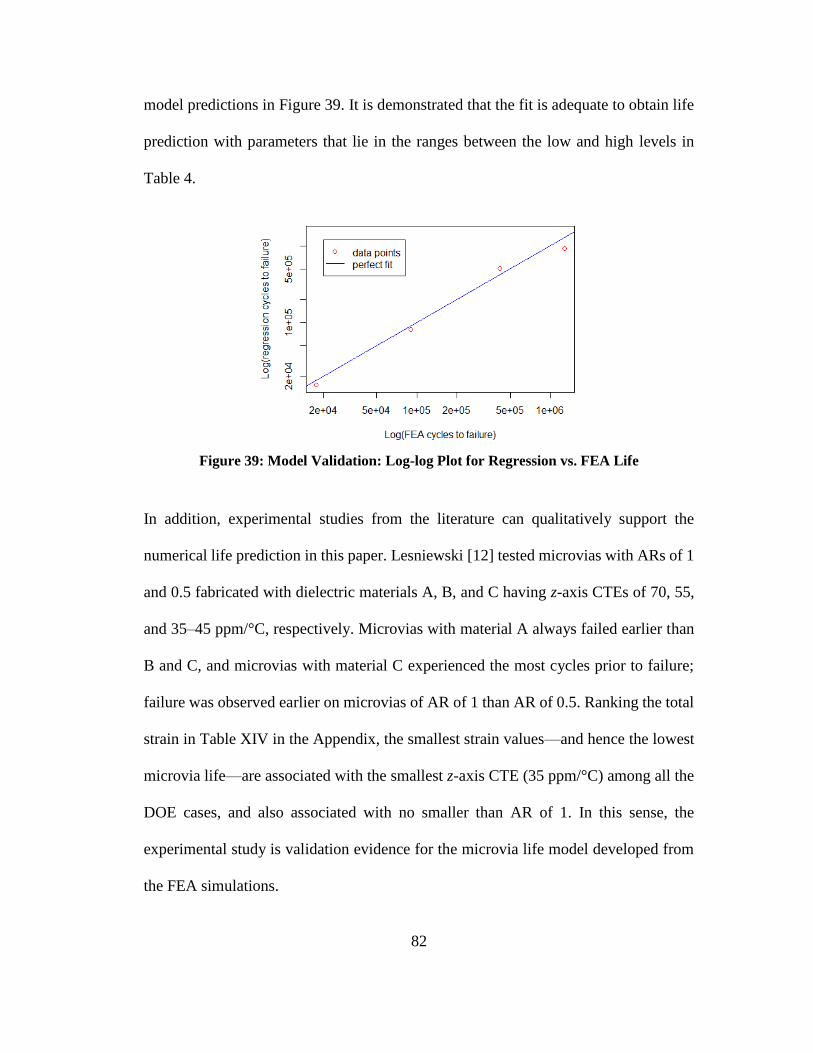
82
model predictions in Figure 39. It is demonstrated that the fit is adequate to obtain life
prediction with parameters that lie in the ranges between the low and high levels in
Table 4.
Figure 39: Model Validation: Log-log Plot for Regression vs. FEA Life
In addition, experimental studies from the literature can qualitatively support the
numerical life prediction in this paper. Lesniewski [12] tested microvias with ARs of 1
and 0.5 fabricated with dielectric materials A, B, and C having z-axis CTEs of 70, 55,
and 35–45 ppm/°C, respectively. Microvias with material A always failed earlier than
B and C, and microvias with material C experienced the most cycles prior to failure;
failure was observed earlier on microvias of AR of 1 than AR of 0.5. Ranking the total
strain in Table XIV in the Appendix, the smallest strain values—and hence the lowest
microvia life—are associated with the smallest z-axis CTE (35 ppm/°C) among all the
DOE cases, and also associated with no smaller than AR of 1. In this sense, the
experimental study is validation evidence for the microvia life model developed from
the FEA simulations.
83
Summary
This study has examined the design, material, and process parameters that affect
microvia reliability, and developed a second-order regression model to predict the
cycles-to-failure of copper-filled stacked microvias under thermal loading. This life
prediction model uses dielectric thickness, microvia diameter, z-axis CTE, z-axis
modulus, and void size as inputs to predict the total strain using Eq. (11), and then solve
the fatigue life of the microvia using the combined Basquin and Coffin–Manson Eq.
(5). The electronics industry can use this model as a convenient and inexpensive tool
for HDI design validation and board qualification. This is the first known regression
model for stacked microvia life prediction.
The prediction model captures the nonlinear relationship between the total strain and
the critical microvia parameters. The comparison of the developed second-order model,
Eq. (11) with first-order models demonstrated that the second-order model predicted
much more accurate total strain than first-order models. The life predictions from the
developed model were found to agree closely with the cycles-to-failure from the DOE
results. Robustness of the model was validated by using test parameter values that were
not included in the original DOE. The developed model was proven to be sufficiently
accurate and robust to predict microvia life within the limitations of the combined
Basquin and Coffin–Manson equation.
Early in the HDI board design stage, the microvia life prediction model can be used to
determine if a certain design satisfies the expected reliability or to compare different

84
designs. Given the design geometry, material properties, and process control capability
(expected voiding defects), a quick calculation of microvia fatigue life can be
performed using the developed model. This will reduce the need for costly prototypes
or test coupons, prolonged testing, and time spent for numerical simulation and
analysis. Based on the predicted microvia fatigue life, a reliable design and material
selection can be achieved through virtual “design-build-test-improve” cycles. Even
when the microvia life prediction model is paired with reliability testing, especially for
microvias used in high-reliability applications, the model can reduce the amount of
testing needed to arrive at an optimized design.
The life prediction model accounts for not only the microvia design parameters and
material properties, but also defects (microvia voiding) introduced during the
manufacturing process. The model can predict cycles-to-failure of microvias without
voids and with voids of different sizes. Thus, this model can be used to determine if a
batch of HDI boards can be accepted when voiding occur in the microvias, and if a
plating process is acceptable for a HDI board design in terms of the voids generated
from the process.
The regression model for microvia life prediction should be used with caution. Firstly,
the region of applicability of the model is subject to the accuracy of the combined
Basquin and Coffin–Manson equation for electrolytic copper, from approximately 101
cycles to 106 cycles-to-failure. Secondly, the regression should not be used to

85
extrapolate for parameter values that lie outside of the ranges used in the creation of
the regression model (the parameter value ranges are listed in Table 4). The parameter
ranges selected for the DOE were intentionally designed to enable the model to have
applicability to both current and anticipated future microvia technologies.

86
Fracture Analysis for Microvia Interface Separation
The poor quality of electroless copper results in weak bond between the microvia base
and the target pad, and hence the interface separation. The microvia interface separation
may occur at three potential locations as demonstrated in Figure 40 —1) at the interface
of the electroless copper and the target pad (electrolytic copper), 2) at the interface of
the microvia base (electrolytic copper) and the electroless copper, or 3) within the
electroless copper layer. Lesniewski [12] closely examined the interface separation,
and observed that the separation was within the electroless copper layer from his testing
samples. As the first study to quantitatively investigate the microvia separation issue,
this work focused on the separation due to fracture within the electroless copper layer.
Fracture analysis using FEA was conducted to calculate the fracture mechanics
parameter in the electroless copper layer.
Figure 40: Three Potential Microvia Interface Separation Locations

87
Fracture Analysis and Numerical Calculation
In the fracture analysis, an initial crack is present, simulating a structure flaw. The
fracture mechanics parameters, such as energy release rate and stress intensity factor
are usually used to characterize the fracture. In this study, the researcher evaluated the
energy release rate, G at the pre-existing crack tip in the electroless copper layer in
the microvia structure. Given the critical energy release rate cG and fracture criterion,
it can be determined whether the crack propagates.
There are three fracture modes, opening mode, shearing (or sliding) mode, and tearing
mode [51]. The diagram of the three fracture modes are shown in Figure 41. The
fracture criterion is a function of Mode I, Mode II, and Mode III fracture mechanics
parameters. Using energy release rate for fracture analysis, the fracture criterion can be
expressed as
( , , , , , )c c c
I II III I II IIIf f G G G G G G (12)
where IG , IIG , and IIIG are Mode I, II and III energy release rate, respectively, and
c
IG , c
IIG , and c
IIIG are critical Mode I, II and III energy release rate, respectively.
Fracture occurs when the energy release rate at the crack tip meets the criterion.

88
Figure 41: Three Fracture Modes [51]
The commercial finite element modeling software, Ansys has multiple fracture criteria
available. The criteria include Critical Energy Release Rate Criterion, Linear Fracture
Criterion, Bilinear Fracture Criterion, B-K Fracture Criterion, Modified B-K Fracture
Criterion, Power Law Fracture Criterion, and User-Defined Fracture Criterion [52].
The researcher used the Critical Energy Release Rate Criterion in this study to
determine the likelihood of microvia interface separation. In the Critical Energy
Release Rate Criterion,
T
c
T
Gf
G (13)
where T I II IIIG G G G is the total energy release rate, and c
TG is the critical energy
release rate. The recommended f value in Ansys for fracture to occur is 0.95 to 1.05,
and the default is 1.0. That means, by default, when TG equals to c
TG , the initial crack
propagates.

89
The energy release rate were calculated using the virtual crack-closure technique
(VCCT) from Ansys software in this study. VCCT assumes that the energy needed to
separate a surface is the same as the energy needed to close the same surface. The
numerical calculation of the energy release rate in a 2D geometry is as in Eq. (14) and
(15):
1
2I yG R
a (14)
1
2II xG R u
a (15)
where u and v are relative displacement between the top and bottom nodes of the
crack face in local coordinate x, and y, respectively, xR and yR approximates the
reaction forces at the crack tip node, and a is the crack extension. The 2D crack
geometry schematic is shown in Figure 42.

90
Figure 42: 2D Crack Geometry Schematic
2D Finite Element Modeling
To model the microvia structure using a 2D geometry, a cylindrical unit cell was
isolated from the HDI board (Figure 43). In this case, the 2D axial section can be used
for the microvia model due to axisymmetry. Periodical boundary conditions were
applied on the outer cylindrical boundary of the unit cell.
Figure 43: Cylindrical Unit Cell
Unit cell
Equivalent medium with
uniform density of
microvias

91
A two-level stacked microvia is modeled in this study. The thermo-mechanical stress
analysis indicates that maximum stress is located at the bottom corner of the lower level
microvia. Therefore, the electroless copper in the lower level microvia was the potential
site for interface separation. Consequently, only the electroless copper layer in the
lower microvia level was simulated in the finite element model, and the other part of
the microvia was simplified as electrolytic copper. We focused on the electroless
copper at the lower level bottom corner for fracture analysis.
Half of the axial section of the unit cell was modeled due to symmetry. The 2D model
is shown in Figure 44.
Figure 44: 2D Axisymmetric Model
The same material properties for the electrolytic copper and dielectric material were
used in the fracture analysis as in the stress/strain analysis in Chapter 3 and 4. The
properties of the electroless copper are listed in Table 15.
Electroless copper Initial crack

92
Table 15: Material Properties of Electroless Copper
Material CTE (ppm/oC) Young’s Modulus (GPa) Poisson’s Ratio
Copper (Isotropic) 17 127 0. 34
Figure 45 shows the meshing result of the axisymmetric model. The meshing on the
electroless copper is much finer than that on the other part of the model.
Figure 45: Meshing Result of the Axisymmetric Model
To understand the likelihood of fracture, different loading conditions and initial crack
lengths were simulated. The loading conditions were monotonic thermal loading, 25 ºC
to125 ºC and 25 ºC to 260 ºC, which simulated the accelerated testing and solder reflow
conditions, respectively. The initial crack length varied from 1 µm, to 15 µm in the
simulation to examine its effect to energy release rate.
Initial crack

93
Results and Discussion
The total energy release rate predicts the likelihood of fracture. According to the
Critical Energy Release Rate Criterion, when the value of the total energy release rate,
I IIG G G (The Mode III energy release rate was assumed to be zero in the 2D
axisymmetric model.) calculated from the crack tip in the electroless copper layer
exceeds the total critical energy release rate, CG , the initial crack will grow and the
fracture/interface separation will finally occur.
The total energy release rate results are shown in Figure 46. The 25 °C to 260 °C
loading always resulted in higher energy release rate for different initial crack length.
Therefore, the higher the loading temperature, the larger the energy release rate. Solder
reflow is a severer condition for microvia interface separation than accelerated testing
condition. Also, the energy release rate increases with the initial crack length for both
thermal loading conditions. Given the critical energy release rate of electroless copper,
it can be determined whether the initial crack propagates.

94
Figure 46: Total Energy Release Rate
There is no good database available for electroless copper material properties. The
researcher referred to general copper critical energy release rate from the literature. The
copper critical energy release rate varies a lot depending on the dimension and
preparation or manufacturing method of the test specimens. The copper critical energy
release rate can be as low as 1.8 J/m2, or as high as 600 J/m2 [53]-[57][56]. Considering
that electroless copper is more brittle than copper fabricated in other ways, such as
electrolytic copper or rolled copper, the critical energy release rate of electroless copper
can be at the lower range of the literature values, or even lower than the above
mentioned range. It is interesting to measure electroless copper critical energy release
rate, in order to have a more accurate understanding of the microvia interface
separation.
The Model I and Mode II energy release rates were plotted as in Figure 47. According
to the result, Model II energy release rate dominates for both 25 °C to 260 °C and 25 °C

95
to 125 °C loading conditions. Therefore, the shearing fracture contributes more in
microvia interface separation. It is interesting for the 25 °C to 260 °C loading. Although
Mode I energy release rate decreases with initial crack length, the total energy release
rate still increases. This phenomenon is due to the complex geometry and thermal
loading in the microvia structure.
Figure 47: Mode I and Mode II Energy Release Rate
In the fracture analysis, the electroless copper was assumed to be purely elastic, because
it is a brittle material. It is worth to discuss the effect of the assumption. In case
plasticity occurs in the electroless copper (all other conditions are unchanged), the
stress resulted from the thermal loading is lower than in the pure elastic scenario (Under
a specific thermal loading, the strain in the electroless copper is determinate due to the
CTE mismatch. However, the stress resulted from the strain is lower if the electroless
copper is an elastic-plastic material, compared with pure elastic assumption.). Hence,
the reaction force at the crack tip may be higher for the pure elastic case, as compared
to the case where plasticity is included. Because energy release rate is proportional to

96
the reaction force as shown in Eq. (14) and Eq. (15), the pure elasticity assumption of
the electroless copper may result in larger energy release rate calculation result than
reality. Therefore, there may be more chance that we predict the crack to grow than not
under the pure elasticity assumption.
Summary
This is the first known study on interface separation between microvia base and target
pad using fracture analysis. A higher thermal load always results in a larger energy
release rate—more likely to fracture and separate. According to the study, the solder
reflow thermal loading resulted in 1.6 – 2.3 times larger energy release rate than the
accelerated test loading, when the electroless copper layer has a pre-existing crack of 2
m – 15 m; 10.4 times larger energy release rate when the pre-existing crack is 1 m.
A larger initial crack length resulted in a higher energy release rate, and therefore, an
existing crack (structure flaw) tends to continue growing once the fracture starts,
resulting in microvia interface separation. Mode II fracture dominates the interface
separation in the microvia structure.

97
Contributions and Suggestions for Future Research
The electronics industry faces challenges to fabric the small size dead-end microvias
in HDI boards. Voids can be easily generated from copper plating process in the
copper-filled microvias. When voids are present, localized stress concentration on the
electrodeposited copper structure can degrade the reliability of microvias. Poor quality
of electroless copper results in weak bond between the microvia base and the target pad
interface, and therefore, interface separation is a commonly observed failure in HDI
boards.
However, the reliability research and qualification method on microvias lagged behind.
There was neither sufficient work on copper-filled stacked microvia reliability study,
nor analysis of the effect of manufacturing defects on copper-filled microvias.
This dissertation has determined the effects of voids on the lifetime of copper-filled
stacked microvias, and further develop a regression model that the electronics industry
can use to predict microvia fatigue life and assess risks associated with the design and
production of the latest generation of HDI circuit boards. The dissertation has also
quantitatively discussed the factors that affect microvia interface separation.
Contributions of this Dissertation
The most significant contributions made in this dissertation are:

98
1) First study to determine the effects of voids on the thermomechanical reliability
of copper-filled microvias with different HDI design parameters
a. With a parametric study, it is quantitatively determined how different
void shapes, sizes, and locations affect the lifetime of copper-filled
microvias with different microvia geometry parameters and dielectric
material properties.
b. It is revealed that void acceptance criterion (25% area ratio) from the
IPC-6012D-RedLine Standard is not correct for stacked microvias.
c. The researcher has determined the void acceptance criterion is 14% area
ratio for 3-level stacked microvias, and 9% area ratio for 5-level stacked
microvia.
d. A microvia virtual qualification method is proposed for HDI board
design and process qualification to reduce the need for multiple “design-
build-test-improve” cycles.
2) First strain life prediction model for copper-filled stacked microvias
a. The researcher has developed a regression life model for fatigue life
prediction of copper-filled three-level stacked microvias.
b. The life prediction model captures the second-order relationship
between the input variables (microvia design parameters, material
properties, as well as void size) and the total strain that is used for
fatigue life estimation.
c. The regression model takes the form of

99
∆𝜀 = 106(-5835+147.6A+170.9E+285.9V-0.716TD+2.324TA-
1.552DA-2.167DV+0.4781𝐷2)
3) First fracture analysis on microvia interface separation
a. The researcher has quantitatively determined how a structure flaw
(initial crack length) in the electroless copper affect the likelihood of
microvia interface separation under different thermal loading
conditions.
The contributions of this dissertation provide tools and guidelines for the electronics
industry in HDI board design and process qualification and HDI board reliability
assessment. The void acceptance criterion established from the dissertation helps the
electronics industry to make correct and prompt decisions on the acceptance/rejection
of a batch of HDI boards. The virtual qualification method reduces the amount of HDI
board reliability and qualification testing and cut overall development time and cost.
The electronics industry can use the regression life model as a convenient and
inexpensive tool for HDI design and process validation.
Suggestions for Future Research
The parametric study and DOE in this dissertation were performed with FEA
simulations. A suggestion for future research is to design microvia test coupons with
different geometry parameters, dielectric materials, and defect variables to verify the
effects of voids and the regression microvia life prediction model. The future work will
further promote the value of this dissertation.

100
As a common failure mode, the microvia interface separation is worth of more attention
and future studies. Here are some suggestions on the interface separation study. As the
first study on microvia interface separation, the researcher focused on crack growth
under a single thermal loading, while cyclic loading conditions further affect the crack
propagation. Next, it is valuable to measure electroless copper critical fracture
mechanic parameters (e.g. critical energy release rate and critical stress intensity factor)
in order to have an accurate prediction of microvia interface separation. Also,
electroless copper grain size affects the critical fracture mechanic parameters and the
crack growth process. Therefore, electroless copper process quality and capability
should be incorporated into the interface separation study. Additionally, it is interesting
to study the delamination on the interface between electroless copper and electrolytic
copper (on microvia base or target pad), as well as estimate the competing failure
mechanisms of the interface delamination and fracture within electroless copper.

101
Appendices
Table A.I: Box–Behnken Design of the Experiments with Five Factors
Experiment # Dielectric
thickness
Microvia
diameter
z-axis
CTE
z-axis
modulus Void size
1 –1 –1 0 0 0
2 1 –1 0 0 0
3 –1 1 0 0 0
4 1 1 0 0 0
5 –1 0 –1 0 0
6 1 0 –1 0 0
7 –1 0 1 0 0
8 1 0 1 0 0
9 0 0 –1 –1 0
10 0 0 1 –1 0
11 0 0 –1 1 0
12 0 0 1 1 0
13 0 0 0 –1 –1
14 0 0 0 1 –1
15 0 0 0 –1 1
16 0 0 0 1 1
17 0 –1 0 0 –1
18 0 1 0 0 –1
19 0 –1 0 0 1
20 0 1 0 0 1
21 –1 0 0 –1 0
22 1 0 0 –1 0
23 –1 0 0 1 0
24 1 0 0 1 0
25 –1 0 0 0 –1
26 1 0 0 0 –1
27 –1 0 0 0 1
28 1 0 0 0 1
29 0 –1 –1 0 0
30 0 1 –1 0 0
31 0 –1 1 0 0

102
32 0 1 1 0 0
33 0 –1 0 –1 0
34 0 1 0 –1 0
35 0 –1 0 1 0
36 0 1 0 1 0
37 0 0 –1 0 –1
38 0 0 1 0 –1
39 0 0 –1 0 1
40 0 0 1 0 1
41 0 0 0 0 0
Table A.II: Parameters and FEA Results of the 41 Experiments
Experiment # T (µm) D (µm) A (ppm/°C) E (GPa) V (%) Total strain
1 25 50 52.5 7 8 0.003586
2 75 50 52.5 7 8 0.009379
3 25 150 52.5 7 8 0.001385
4 75 150 52.5 7 8 0.002581
5 25 100 35 7 8 0.000811
6 75 100 35 7 8 0.001793
7 25 100 70 7 8 0.002580
8 75 100 70 7 8 0.006756
9 50 100 35 3 8 0.001020
10 50 100 70 3 8 0.003134
11 50 100 35 11 8 0.001575
12 50 100 70 11 8 0.005645
13 50 100 52.5 3 0 0.001833
14 50 100 52.5 11 0 0.002957
15 50 100 52.5 3 16 0.002450
16 50 100 52.5 11 16 0.003949
17 50 50 52.5 7 0 0.003466
18 50 150 52.5 7 0 0.002023

103
19 50 50 52.5 7 16 0.007159
20 50 150 52.5 7 16 0.002031
21 25 100 52.5 3 8 0.001208
22 75 100 52.5 3 8 0.002836
23 25 100 52.5 11 8 0.001977
24 75 100 52.5 11 8 0.004560
25 25 100 52.5 7 0 0.001615
26 75 100 52.5 7 0 0.003279
27 25 100 52.5 7 16 0.001864
28 75 100 52.5 7 16 0.004296
29 50 50 35 7 8 0.002447
30 50 150 35 7 8 0.000999
31 50 50 70 7 8 0.010773
32 50 150 70 7 8 0.003240
33 50 50 52.5 3 8 0.004331
34 50 150 52.5 3 8 0.001437
35 50 50 52.5 11 8 0.006029
36 50 150 52.5 11 8 0.002491
37 50 100 35 7 0 0.001164
38 50 100 70 7 0 0.003916
39 50 100 35 7 16 0.001586
40 50 100 70 7 16 0.005771
41 50 100 52.5 7 8 0.002776

104
Bibliography
[1] K. Jonsson and B. Andersson. HDI = High Density Interconnect, IPC
Presentation. NCAB Group. [Online] Available:
http://www.dnu.no/arkiv3/HDI%20-IPC%20presentation_Norge%20090924-
2.pdf
[2] Happy Holden et al., The HDI Handbook, 1st ed., Seaside: BR Publishing, Inc.,
2009.
[3] iNEMI Technology Roadmaps, “INTERCONNECTION PCB – ORGANIC”,
2017.
[4] Design Guide for High Density Interconnects (HDIs) and Microvias, IPC/JPCA-
2315, Jun. 2000.
[5] Sectional Design Standard for High Density Interconnect (HDI) Printed Boards,
IPC-2226, Apr. 2003.
[6] J.H. Lau and C. Chang, “An overview of microvia technology,” Circuit World,
vol. 22, no. 2, pp. 22-32, 2000.
[7] B. Birch, “Reliability testing for mcrovias in printed wire boards”, Circuit World,
vol. 35, no. 4, pp. 3–17, 2009.
[8] R. Soares, J. Haque, and Ed Prado, “High-density PWB microvia reliability for
space application”, in Proc. 2007 IEEE Aerospace Conference, Big Sky, MT,
Mar. 2007, pp. 1 – 8.

105
[9] R. Ghaffarian, “Reliability of PWB microvias for high density package
assembly,” International Journal of Materials and Structural Integrity, vol. 2,
nos. 1/2, pp. 47-63, 2008.
[10] B. Xiong, K. W. Loo, and K. Nagarajan, “Microvia reliability improvement for
high density interconnect substrate,” in Proc. 13th IEEE Electronics Packaging
Technology Conference (EPTC), Singapore, Singapore, Dec. 2011, pp. 138 –141.
[11] R. Bakhshi, M. Azarian, and M. Pecht, “Effects of voiding on the degradation of
microvias in high density interconnect printed circuit boards under
thermomechanical stresses,” IEEE Transactions on Components, Packaging and
Manufacturing Technology, vol. 4, no. 8, pp. 1374-1379, 2014.
[12] T. Lesniewski, “Effects of dielectric material, aspect ratio and copper plating on
microvia reliability,” in Proc. IPC APEX Technical Conference, Las Vegas, NV,
Mar. 25-27, 2014, Paper No. S19-01.
[13] P. Reid. (Aug., 2012). Test method improves PWB reliability. PWB Interconnect
Solutions. [Online]. Available: http://www.edn.com/design/test-and-
measurement/4391618/Test-method-improves-PWB-reliability
[14] L. Ji and Z. Yang, “Analysis of cracking blind vias of PCB for mobile phones,”
in Proc. International Conference on Electronic Packaging Technology & High
Density Packaging, Shanghai, China, Jul. 2008.
[15] Thermal Shock, Continuity and Microsection, Printed Board, IPC-TM-650
2.6.7.2B, May 2004.

106
[16] J. Rasul, W. Bratschun, and J. McGowen, “Microvia bare board reliability
assessment,” in Proc. IPC Expo Technical Conference, San Jose, CA, Mar. 9-13,
1997, Paper No. S17-5.
[17] J. Davignon, “Final report of the October project/ITRI microvia project,” in Proc.
IPC Expo Technical Conference, San Jose, CA, Mar. 9–13, 1997, Paper No. S17-
6.
[18] F. Liu, J. Lu, V. Sundaram, D. Sutter, G. White, D. F. Baldwin, and R. R.
Tummala, “Reliability assessment of microvias in HDI printed circuit board”,
IEEE Trans. Compon. Packag. Manuf. Technol., vol. 25, no. 2, pp. 254–259, Jun.
2000.
[19] G. Ramakrishna, F. Liu, and S. K. Sitaramana, “Experimental and numerical
investigation of microvia reliability,” in Proc. ITHERM, 2002, pp. 932–939.
[20] G. Ramakrishna, F. Liu, and S. K. Sitaramana, “Role of dielectric material and
geometry on the thermo-mechanical reliability of microvias,” in Proc. ECTC,
2002, pp. 439–445.
[21] F. Liu, V. Sundaram, H. Chan, G. Krishnan, J. Shang, J. Dobrick, J. Neill, D.
Baars, S. Kennedy, and R. Tummala, “Ultra-high density, thin core and low loss
organic system-on-package (SOP) substrate technology for mobile applications,”
in Proc. ECTC, San Diego, CA, May 2009, pp. 612–617.
[22] H. Heer and R. Wong, “Reliability of stacked microvia,” in Proc. IPC APEX
Technical Conference, Las Vegas, NV, Mar. 25-27, 2014, Paper No. S19-03.
[23] DC Current Induced Thermal Cycling Test, IPC-TM-650 2.6.26, May 2001.

107
[24] P. Andrews, G. Parry, P. Reid. (2005). Microvia reliability: Concerns in the lead
free assembly environment. Joint paper by Curtiss-Wright Controls Embedded
Computing, Coretec Inc., and PWB Interconnect Solution Inc. [Online].
Available: http://www.pwbcorp.com/images/Whitepapers/Microvia.pdf
[25] Moisture/Reflow Sensitivity Classification for Nonhermetic Solid State Surface
Mount Devices, IPC/JEDEC J-STD-020D.1, Mar. 2008.
[26] R. Bakhshi, M. H. Azarian, and M. G. Pecht, “Effects of Voiding on the
Degradation of Microvias in High Density Interconnect Printed Circuit Boards
Under Thermomechanical Stresses,” IEEE Trans. Compon. Packag. Manuf.
Technol., vol. 4, no. 8, pp. 1374–1379, Aug. 2014.
[27] A. S. Prabhu, D. B. Barker, M. G. Pecht, J. W. Evans, W. Grieg, E. S. Bernard,
and E. Smith, “A thermo-mechanical fatigue analysis of high density interconnect
vias,” in Proc. INTERpack, Lahaina, HI, Mar. 26-30, 1995, pp. 187–216.
[28] A. O. Ogunjimi, S. MacGregor M. G. Pecht, and J. W. Evans, “The effect of
manufacturing and design process variabilities on the fatigue life of the high
density interconnect vias,” J. Electron. Manuf., vol. 5, no. 2, pp. 111–119, Jun.
1995.
[29] T. Wang and Y. Lai, “Stress analysis for fracture potential of blind via in a build-
up substrate,” Circuit World, vol. 32, no. 2, pp. 39–44, 2006.
[30] J. Wang, J. Zhu, S. Quander, T. Reinikainen, and P. Viswanadham, “Microvia
fatigue life prediction under thermo-mechanical cyclic loading condition,” in
Proc. NEPCON West - Fiberoptic Expo Conference, Dec. 2002, pp. 53–60.

108
[31] Y. Ko, H. Park, G. Park, and S. Cho, “A study on the reliability of micro-vias in
printed circuit boards during thermal cycling,” Advanced Science Letters, vol. 19,
pp. 3683–3687, 2013.
[32] K. V. Sexton, “Formulation of simple model to assess microvia thermal cycle
fatigue life,” M.S. Thesis, Dept. Mech. Eng., Univ. of Maryland, College Park,
MD, 2001.
[33] Qualification and Performance Specification for Rigid Printed Boards, IPC-
6012D-RedLine, Sep. 2015.
[34] T. Kinoshita, T. Kawakami, T. Hori, K. Matsumoto, S. Kohara, Y, Orii, F.
Yamada, and M. Kada, “Thermal stresses of through silicon vias and Si chips in
three dimensional system in package,” Journal of Electronic Packaging, vol. 134,
No. 2. Jun 2012.
[35] T. Kinoshita, T. Sugiura, T. Kawakami, K. Matsumoto, S. Kohara, and Y. Orii,
“Thermal stress around void in through silicon via in 3D Sip,” in Proc.
International Conference on Electronics Packaging (ICEP), pp. 105-108, Apr.
23–25, 2014.
[36] Y. Sun, H. Kim, Y. Wang, G. Ding, J. Zhao, and H. Wang, “Thermal effect of
TSV (through silicon via) with void,” in Proc. 16th Electronics Packaging
Technology Conference (EPTC), pp. 307–312, Dec. 3-5, 2014.
[37] X. Liu, Q. Chen, V. Sundaram, S. Muthukumar, R. R. Tummala, and S. K
.Sitaraman1, “Reliable design of electroplated copper through silicon vias,” in

109
Proc. the ASME 2010 International Mechanical Engineering Congress &
Exposition (IMECE2010), Nov. 12–18, 2010.
[38] S. M. Bhandarkar, A. Dasgupta, D. Barker, and M. Pecht, “Effect of voids in
solder-filled plated through holes,” in Proc. IPC 33rd Annual Meeting, Apr. 1–6,
1990
[39] S. M. Bhandarkar, A. Dasgupta, D. Barker, M. Pecht, and W. Engelmaier,
“Influence of selected design variables on thermal-mechanical stress distributions
in plated-through-hole structures,” Journal of Electronic Packaging, vol. 114, no.
1, pp. 8–13, Mar. 1992.
[40] A. Dasgupta and V. Ramappan, “Simulation of the influence of manufacturing
quality on reliability of vias,” Journal of Electronic Packaging, vol. 117, no. 2,
pp. 141–146, Jun, 1995.
[41] Elite Material Co., Ltd., “Lead-free, halogen-free material EM-285 / EM-285B,”
[Online]. Available: http://www.emctw.com/upload/media/Product/CCL/EM-
285.pdf
[42] A. Dasgupta, S. M. Bhandarkar, D. Barker, and M. Pecht, “Thermoelastic
properties of woven-fabric composites using homogenization techniques,” in
Proc. American Society for Composites Technical Conference, pp. 1001–1010,
1990.
[43] F. Su, R. Mao, J. Xiong, K. Zhou, Z. Zhang, J. Shao, and C. Xie, “On thermo-
mechanical reliability of plated-through-hole (PTH),” Microelectronics
Reliability, vol. 52, no. 6, pp. 1189–1196, 2012.

110
[44] W. Engelmaier, “A method for the determination of ductility for thin metal
materials,” ASTM Special Technical Publication, pp. 279–295, 1982.
[45] M. A. Miner, “Cumulative damage in fatigue,” J. Appl. Mech., vol. 12, pp. 159–
164, 1945.
[46] L. J. Ladani and A. Dasgupta, “Effects of voids on thermomechanical durability
of Pb-free BGA solder joints: modeling and simulation,” Journal of Electronic
Packaging, vol. 129, pp. 273–277, 2007.
[47] R. Iannuzzeli, “Predicting plated-through-hole reliability in high temperature
manufacturing processes,” in Proc. ECTC, Atlanta, GA, May 11–16, 1991, pp.
410–421.
[48] Qualification and Performance Specification for High Density Interconnect
(HDI) Layers or Boards, IPC-6016, May 1999.
[49] G. E. P. Box and D. W. Behnken, “Some new three level design for the study of
quantitative variables,” Technometrics, vol. 2, no. 4, pp. 455–475, Nov. 1960.
[50] R. V. Lenth, “Response-Surface Methods in R, Using RSM,” J. Stat Softw, vol.
32, no. 7, Oct. 2009.
[51] C. T. Sun and Z-H Jin, Fracture Mechanics. Waltham Mass.: Butterworth-
Heinemann/Elsevier, 2012
[52] Ansys Manual, “Fracture analysis guide,” Mechanical APDL, Ansys 16.2.
[53] G. H. Lee, J. H. Kim, and H. G. Beom, “Size dependence of the fracture toughness
of copper nanostrips under tension,” Journal of Mechanical Science and
Technology, Vol. 30, No. 6. pp. 2497 – 2505, 2016.

111
[54] H. Hirakata, T. Yoshida, T. Kondo, and K. Minoshima, “Effects of film thickness
on critical crack tip opening displacement in single-crystalline and polycrystalline
submicron Cu films,” Engineering Fracture Mechanics, Vol. 159, pp. 98 – 114,
2016.
[55] H. Hirakata, O. Nishijima, N. Fukuhara, T. Kondo, A. Yonezu, and K.
Minoshima,“Size effect on fracture toughness of freestanding copper nano-
films,” Materials Science and Engineering A, Vol. 528, pp. 8120 – 8127, 2011.
[56] M. R. Begley, O. N. Scott, M. Utz, and H. Bart-Smith, “Fracture of nanoscale
copper films on elastomer substrates,” Applied Physics Letters, Vol. 95, pp.
231914, 2009.
[57] A. Singh, L. Tang, M. Dao, L. Lub, and S. Suresh, “Fracture toughness and
fatigue crack growth characteristics of nanotwinned copper,” Acta Materialia,
vol. 59, pp. 2437–2446, 2011.