a/d flash mcu with eeprom · 10-bit ptm × 1 part no. time base sim uart cmp scom/ sseg sseg led...
TRANSCRIPT

A/D Flash MCU with EEPROM
HT66F0175/HT66F0185
Revision: V1.50 Date: ����st ��� �01�����st ��� �01�

Rev. 1.50 � ����st ��� �01� Rev. 1.50 3 ����st ��� �01�
HT66F0175/HT66F0185A/D Flash MCU with EEPROM
HT66F0175/HT66F0185A/D Flash MCU with EEPROM
Table of Contents
Features ................................................................................................................ 7CPU Feat�res ..............................................................................................................................�Peripheral Feat�res ......................................................................................................................�
General Description ............................................................................................. 8Selection Table ..................................................................................................... 8Block Diagram ...................................................................................................... 9Pin Assignment .................................................................................................... 9Pin Descriptions ................................................................................................ 11Absolute Maximum Ratings .............................................................................. 17D.C. Characteristics ........................................................................................... 17A.C. Characteristics ........................................................................................... 19HIRC Electrical Characteristics ........................................................................ 20A/D Converter Electrical Characteristics ......................................................... 21LVD/LVR Electrical Characteristics .................................................................. 22Comparator Electrical Characteristics ............................................................ 22Software Controlled LCD Driver Electrical Characteristics ........................... 23Power-on Reset Characteristics ....................................................................... 23System Architecture .......................................................................................... 24
Clockin� and Pipelinin� ..............................................................................................................�4Pro�ram Co�nter ........................................................................................................................�5Stack ..........................................................................................................................................�6�rithmetic and Lo�ic Unit – �LU ................................................................................................�6
Flash Program Memory ..................................................................................... 27Str�ct�re .....................................................................................................................................��Special Vectors ..........................................................................................................................��Look-�p Table .............................................................................................................................��Table Pro�ram Example .............................................................................................................��In Circ�it Pro�rammin� – ICP ....................................................................................................�9On-Chip Deb�� S�pport – OCDS ..............................................................................................30
Data Memory ...................................................................................................... 31Str�ct�re .....................................................................................................................................31
Special Function Register Description ............................................................ 33Indirect �ddressin� Re�isters – I�R0� I�R1 ..............................................................................33Memory Pointers – MP0� MP1 ...................................................................................................33Bank Pointer – BP ......................................................................................................................34�cc�m�lator – �CC ....................................................................................................................34Pro�ram Co�nter Low Re�ister – PCL .......................................................................................34Look-�p Table Re�isters – TBLP� TBHP� TBLH ..........................................................................34Stat�s Re�ister – ST�TUS .........................................................................................................35
Rev. 1.50 � ����st ��� �01� Rev. 1.50 3 ����st ��� �01�
HT66F0175/HT66F0185A/D Flash MCU with EEPROM
HT66F0175/HT66F0185A/D Flash MCU with EEPROM
EEPROM Data Memory ...................................................................................... 37EEPROM Data Memory Str�ct�re .............................................................................................3�EEPROM Re�isters ...................................................................................................................3�Readin� Data from the EEPROM ..............................................................................................39Writin� Data to the EEPROM .....................................................................................................39Write Protection ..........................................................................................................................39EEPROM Interr�pt .....................................................................................................................39Pro�rammin� Considerations .....................................................................................................40
Oscillator ............................................................................................................ 41Oscillator Overview ....................................................................................................................41System Clock Configurations .....................................................................................................41External Crystal/Ceramic Oscillator – HXT ................................................................................4�Internal Hi�h Speed RC Oscillator – HIRC ................................................................................43External 3�.�6� kHz Crystal Oscillator – LXT ............................................................................43Internal 3�kHz Oscillator – LIRC ................................................................................................44S�pplementary Oscillators .........................................................................................................44
Operating Modes and System Clocks ............................................................. 45System Clocks ...........................................................................................................................45System Operation Modes ...........................................................................................................46Control Re�isters .......................................................................................................................4�Fast Wake-�p .............................................................................................................................49Operatin� Mode Switchin� .........................................................................................................50Standby C�rrent Considerations ................................................................................................54Wake-�p .....................................................................................................................................54Pro�rammin� Considerations .....................................................................................................55
Watchdog Timer ................................................................................................. 55Watchdo� Timer Clock So�rce ...................................................................................................55Watchdo� Timer Control Re�ister ..............................................................................................55Watchdo� Timer Operation ........................................................................................................5�
Reset and Initialisation ...................................................................................... 58Reset F�nctions .........................................................................................................................5�Reset Initial Conditions ..............................................................................................................60
Input/Output Ports ............................................................................................. 64P�ll-hi�h Resistors .....................................................................................................................65Port � Wake-�p ..........................................................................................................................65I/O Port Control Re�isters ..........................................................................................................66I/O Port So�rce C�rrent Control .................................................................................................66Pin-remappin� F�nctions ...........................................................................................................6�I/O Pin Str�ct�res .......................................................................................................................69Pro�rammin� Considerations .....................................................................................................�0

Rev. 1.50 4 ����st ��� �01� Rev. 1.50 5 ����st ��� �01�
HT66F0175/HT66F0185A/D Flash MCU with EEPROM
HT66F0175/HT66F0185A/D Flash MCU with EEPROM
Timer Modules – TM .......................................................................................... 71Introd�ction ................................................................................................................................�1TM Operation .............................................................................................................................�1TM Clock So�rce ........................................................................................................................��TM Interr�pts ..............................................................................................................................��TM External Pins ........................................................................................................................��TM Inp�t/O�tp�t Pin Control Re�ister ........................................................................................�3Pro�rammin� Considerations .....................................................................................................�5
Compact Type TM – CTM .................................................................................. 76Compact TM Operation ..............................................................................................................�6Compact Type TM Re�ister Description.....................................................................................��Compact Type TM Operation Modes .........................................................................................�1
Standard Type TM – STM .................................................................................. 87Standard TM Operation ..............................................................................................................��Standard Type TM Re�ister Description ....................................................................................��Standard Type TM Operation Modes .........................................................................................9�
Periodic Type TM – PTM .................................................................................. 102Periodic TM Operation .............................................................................................................10�Periodic Type TM Re�ister Description ....................................................................................103Periodic Type TM Operation Modes .........................................................................................10�
Analog to Digital Converter ............................................................................ 117�/D Overview ........................................................................................................................... 11��/D Converter Re�ister Description ......................................................................................... 11��/D Inp�t Pins ..........................................................................................................................1�4�/D Reference Volta�e .............................................................................................................1�4�/D Operation ..........................................................................................................................1�4Conversion Rate and Timin� Dia�ram .....................................................................................1�5S�mmary of �/D Conversion Steps ..........................................................................................1�6Pro�rammin� Considerations ...................................................................................................1���/D Transfer F�nction ..............................................................................................................1���/D Pro�rammin� Examples ....................................................................................................1��
Serial Interface Module – SIM ......................................................................... 130SPI Interface ............................................................................................................................130SPI Re�isters ...........................................................................................................................131SPI Comm�nication .................................................................................................................134I�C Interface .............................................................................................................................136I�C Re�isters ............................................................................................................................13�I�C B�s Comm�nication ...........................................................................................................141I�C Time-o�t Control .................................................................................................................144
Rev. 1.50 4 ����st ��� �01� Rev. 1.50 5 ����st ��� �01�
HT66F0175/HT66F0185A/D Flash MCU with EEPROM
HT66F0175/HT66F0185A/D Flash MCU with EEPROM
Comparators .................................................................................................... 146Comparator Operation .............................................................................................................146Comparator Interr�pt ................................................................................................................146Pro�rammin� Considerations ...................................................................................................146
SCOM/SSEG Function for LCD ....................................................................... 148LCD Operation .........................................................................................................................14�LCD Control Re�isters .............................................................................................................150
UART Interface ................................................................................................. 155U�RT External Pin ...................................................................................................................156U�RT Data Transfer Scheme...................................................................................................156U�RT Stat�s and Control Re�isters.........................................................................................156Ba�d Rate Generator ...............................................................................................................16�U�RT Set�p and Control..........................................................................................................163U�RT Transmitter.....................................................................................................................164U�RT Receiver ........................................................................................................................165Mana�in� Receiver Errors .......................................................................................................16�U�RT Interr�pt Str�ct�re..........................................................................................................16�U�RT Power Down and Wake-�p ............................................................................................169
Low Voltage Detector – LVD ........................................................................... 170LVD Re�ister ............................................................................................................................1�0LVD Operation ..........................................................................................................................1�1
Interrupts .......................................................................................................... 172Interr�pt Re�isters ....................................................................................................................1��Interr�pt Operation ...................................................................................................................1�9External Interr�pt ......................................................................................................................1�1Comparator Interr�pt – HT66F01�5 .........................................................................................1�1M�lti-f�nction Interr�pt .............................................................................................................1�1�/D Converter Interr�pt ............................................................................................................1��Time Base Interr�pt ..................................................................................................................1��Serial Interface Mod�le Interr�pt ..............................................................................................1�3U�RT Transfer Interr�pt – HT66F01�5 ....................................................................................1�3LVD Interr�pt ............................................................................................................................1�4EEPROM Interr�pt ...................................................................................................................1�4TM Interr�pt ..............................................................................................................................1�4Interr�pt Wake-�p F�nction ......................................................................................................1�5Pro�rammin� Considerations ...................................................................................................1�5
Configuration Options ..................................................................................... 186Application Circuits ......................................................................................... 186
Rev. 1.50 6 ����st ��� �01� Rev. 1.50 � ����st ��� �01�
HT66F0175/HT66F0185A/D Flash MCU with EEPROM
HT66F0175/HT66F0185A/D Flash MCU with EEPROM
Instruction Set .................................................................................................. 187Introd�ction ..............................................................................................................................1��Instr�ction Timin� .....................................................................................................................1��Movin� and Transferrin� Data ..................................................................................................1���rithmetic Operations ...............................................................................................................1��Lo�ical and Rotate Operation ..................................................................................................1��Branches and Control Transfer ................................................................................................1��Bit Operations ..........................................................................................................................1��Table Read Operations ............................................................................................................1��Other Operations ......................................................................................................................1��
Instruction Set Summary ................................................................................ 189Table Conventions ....................................................................................................................1�9
Instruction Definition ....................................................................................... 191Package Information ....................................................................................... 200
�0-pin SOP (300mil) O�tline Dimensions ................................................................................�01�0-pin SSOP (150mil) O�tline Dimensions ..............................................................................�0��4-pin SOP (300mil) O�tline Dimensions ................................................................................�03�4-pin SSOP (150mil) O�tline Dimensions ..............................................................................�04��-pin SOP (300mil) O�tline Dimensions ................................................................................�05��-pin SSOP (150mil) O�tline Dimensions ..............................................................................�06

Rev. 1.50 6 ����st ��� �01� Rev. 1.50 � ����st ��� �01�
HT66F0175/HT66F0185A/D Flash MCU with EEPROM
HT66F0175/HT66F0185A/D Flash MCU with EEPROM
Features
CPU Features• Operatingvoltage
♦ fSYS=8MHz:2.2V~5.5V♦ fSYS=12MHz:2.7V~5.5V♦ fSYS=20MHz:4.5V~5.5V
• Upto0.2μsinstructioncyclewith20MHzsystemclockatVDD=5V• Powerdownandwake-upfunctionstoreducepowerconsumption• Oscillatortype
♦ ExternalHighSpeedCrystal–HXT♦ External32.768kHzCrystal–LXT♦ InternalHighSpeedRC–HIRC♦ Internal32kHzRC–LIRC
• Fullyintegratedinternal8/12/16MHzoscillatorrequiresnoexternalcomponents• Multi-modeoperation:NORMAL,SLOW,IDLEandSLEEP• Allinstructionsexecutedinonetotwoinstructioncycles• Tablereadinstructions• 63powerfulinstructions• 8-levelsubroutinenesting• Bitmanipulationinstruction
Peripheral Features• ProgramMemory:Upto4K×16• DataMemory:Upto256×8• TrueEEPROMMemory:Upto128×8• WatchdogTimerfunction• Upto26bidirectionalI/Olines• TwoexternalinterruptlinessharedwithI/Opins• MultipleTimerModulesfortimemeasure, inputcapture,comparematchoutput,PWMoutputfunctionorsinglepulseoutputfunction
• SerialInterfacesModule–SIMforSPIorI2C• Softwarecontrolled6-SCOM/SSEGand18-SSEGlinesLCDdriverwith1/3bias• ProgrammableI/OportsourcecurrentforLEDapplications• DualTime-Basefunctionsforgenerationoffixedtimeinterruptsignals• 8-channel12-bitresolutionA/Dconverter• OneComparatorfunction–availableinHT66F0185• Fully-duplexUniversalAsynchronousReceiverandTransmitterInterface–UART,availableinHT66F0185
• Lowvoltageresetfunction• Lowvoltagedetectfunction• Flashprogrammemorycanbere-programmedupto100,000times• Flashprogrammemorydataretention>10years• TrueEEPROMdatamemorycanbere-programmedupto1,000,000times• TrueEEPROMdatamemorydataretention>10years• Widerangeofavailablepackagetypes

Rev. 1.50 � ����st ��� �01� Rev. 1.50 9 ����st ��� �01�
HT66F0175/HT66F0185A/D Flash MCU with EEPROM
HT66F0175/HT66F0185A/D Flash MCU with EEPROM
General DescriptionTheseriesofdevicesareFlashMemoryA/D type8-bithighperformanceRISCarchitecturemicrocontroller.Offeringusers theconvenienceofFlashMemorymulti-programmingfeatures,thesedevicesalsoincludeawiderangeoffunctionsandfeatures.OthermemoryincludesanareaofRAMDataMemoryaswellasanareaoftrueEEPROMmemoryforstorageofnon-volatiledatasuchasserialnumbers,calibratuibdata,etc.
Analogfeaturesincludeamulti-channel12-bitA/Dconverterandacomparatorfunctions.Multipleandextremely flexibleTimerModulesprovide timing,pulsegenerationandPWMgenerationfunctions.Protectivefeaturessuchasan internalWatchdogTimer,LowVoltageResetandLowVoltageDetectorcoupledwithexcellentnoise immunityandESDprotectionensure thatreliableoperationismaintainedinhostileelectricalenvironments.AfullchoiceofHXT,LXT,HIRCandLIRCoscillatorfunctionsareprovidedincludingafullyintegratedsystemoscillatorwhichrequiresnoexternalcomponents for its implementation.Theability tooperateandswitchdynamicallybetweenarangeofoperatingmodesusingdifferentclocksourcesgivesuserstheabilitytooptimisemicrocontrolleroperationandminimizepowerconsumption.
TheinclusionofflexibleI/Oprogrammingfeatures,Time-Basefunctionsalongwithmanyotherfeaturesensurethatthedeviceswillfindexcellentuseinapplicationssuchaselectronicmetering,environmentalmonitoring,handheldinstruments,householdappliances,electronicallycontrolledtools,motordrivinginadditiontomanyothers.
Selection TableMost featuresarecommon toalldevices.Themain featuresdistinguishing themareMemorycapacity,I/Ocount,TimerModulefeatures,SSEGcount,LEDcount,UARTandpackagetypes.Thefollowingtablesummarisesthemainfeaturesofeachdevice.
Part No. Program Memory
Data Memory
Data EEPROM I/O External
Interrupt A/D Timer Module
HT66F01�5 �k × 16 1�� × � 64 × � �� � 1�-bit × � 10-bit PTM × �
HT66F01�5 4k × 16 �56 × � 1�� × � �6 � 1�-bit × �16-bit CTM × 116-bit STM × 110-bit PTM × 1
Part No. Time Base SIM UART CMP SCOM/
SSEG SSEG LED Stack Package
HT66F01�5 � √ — — 6 14 �� � �0/�4SOP/SSOPHT66F01�5 � √ √ √ 6 1� �6 � �4/��SOP/SSOP
Note:Asdevicesexistinmorethanonepackageformat,thetablereflectsthesituationforthepackagewiththemostpins.

Rev. 1.50 � ����st ��� �01� Rev. 1.50 9 ����st ��� �01�
HT66F0175/HT66F0185A/D Flash MCU with EEPROM
HT66F0175/HT66F0185A/D Flash MCU with EEPROM
Block Diagram
8-bitRISCMCUCore
I/O Timer Modules
Flash Program Memory
EEPROMData
Memory
Flash/EEPROM Programming Circuitry
TimeBase
SIM(SPI/I2C)
Low Voltage Reset
Watchdog Timer
Low Voltage Detect
InterruptController
ResetCircuit
External HXT/LXT
Oscillators
12-bit A/DConverter
RAM Data Memory
SSEG/SCOM UART
Internal HIRC/LIRCOscillators
For HT66F0185
+─
For HT66F0185
Comparator
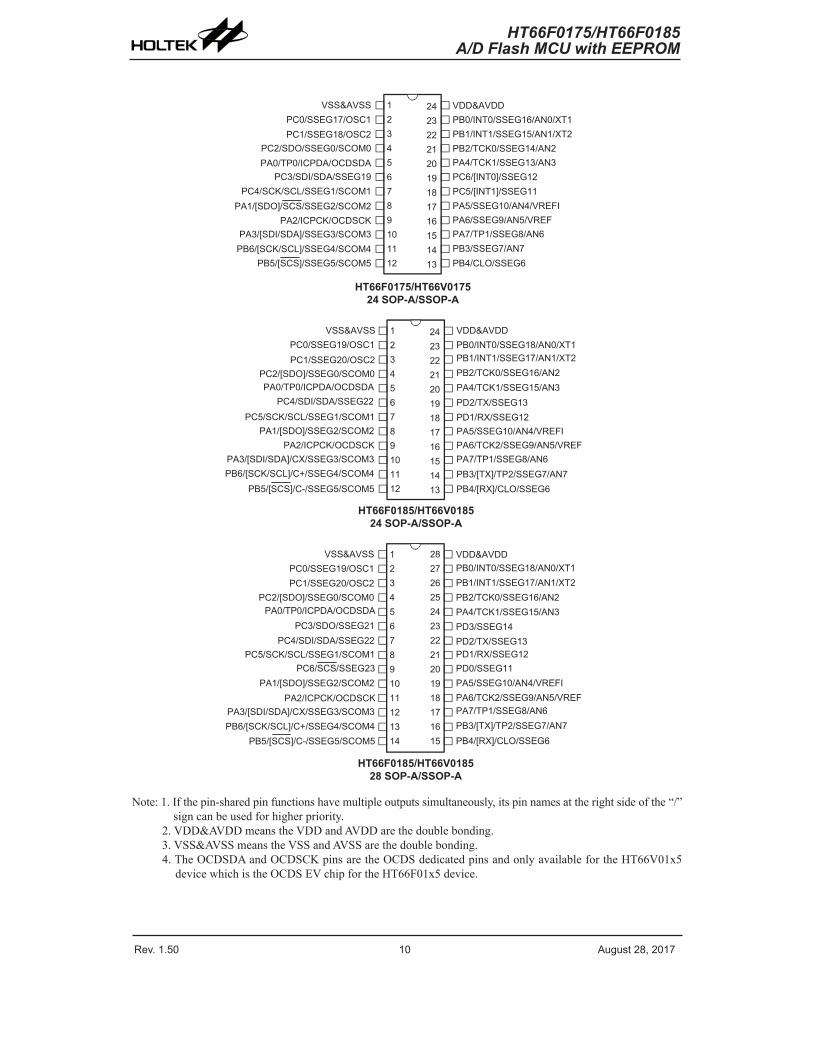
Pin Assignment
HT66F0175/HT66V017520 SOP-A/SSOP-A
�0191�1�161514131�11
1�3456��910
VSS&�VSSPC0/SSEG1�/OSC1PC1/SSEG1�/OSC�
PC�/SDO/SSEG0/SCOM0P�0/TP0/ICPD�/OCDSD�
P��/ICPCK/OCDSCKP�3/[SDI/SD�]/SSEG3/SCOM3
PB6/[SCK/SCL]/SSEG4/SCOM4
P�1/[SDO]/SCS/SSEG�/SCOM�
PB5/[SCS]/SSEG5/SCOM5
VDD&�VDDPB0/INT0/SSEG16/�N0/XT1PB1/INT1/SSEG15/�N1/XT�PB�/TCK0/SSEG14/�N�P�4/TCK1/SSEG13/�N3P�5/SSEG10/�N4/VREFIP�6/SSEG9/�N5/VREFP��/TP1/SSEG�/�N6PB3/SSEG�/�N�PB4/CLO/SSEG6
Rev. 1.50 10 ����st ��� �01� Rev. 1.50 11 ����st ��� �01�
HT66F0175/HT66F0185A/D Flash MCU with EEPROM
HT66F0175/HT66F0185A/D Flash MCU with EEPROM
HT66F0175/HT66V017524 SOP-A/SSOP-A
�4�3���1�0191�1�16151413
1�3456��910111�
VDD&�VDDPB0/INT0/SSEG16/�N0/XT1PB1/INT1/SSEG15/�N1/XT�PB�/TCK0/SSEG14/�N�P�4/TCK1/SSEG13/�N3
P�5/SSEG10/�N4/VREFIP�6/SSEG9/�N5/VREFP��/TP1/SSEG�/�N6PB3/SSEG�/�N�PB4/CLO/SSEG6
PC5/[INT1]/SSEG11PC6/[INT0]/SSEG1�
VSS&�VSSPC0/SSEG1�/OSC1PC1/SSEG1�/OSC�
PC�/SDO/SSEG0/SCOM0P�0/TP0/ICPD�/OCDSD�
P�1/[SDO]/SCS/SSEG�/SCOM�P��/ICPCK/OCDSCK
P�3/[SDI/SD�]/SSEG3/SCOM3PB6/[SCK/SCL]/SSEG4/SCOM4
PB5/[SCS]/SSEG5/SCOM5
PC3/SDI/SD�/SSEG19PC4/SCK/SCL/SSEG1/SCOM1
HT66F0185/HT66V018524 SOP-A/SSOP-A
�4�3���1�0191�1�16151413
1�3456��910111�
VDD&�VDDPB0/INT0/SSEG1�/�N0/XT1PB1/INT1/SSEG1�/�N1/XT�PB�/TCK0/SSEG16/�N�P�4/TCK1/SSEG15/�N3
P�5/SSEG10/�N4/VREFIP�6/TCK�/SSEG9/�N5/VREFP��/TP1/SSEG�/�N6PB3/[TX]/TP�/SSEG�/�N�PB4/[RX]/CLO/SSEG6
PD1/RX/SSEG1�PD�/TX/SSEG13
VSS&�VSSPC0/SSEG19/OSC1PC1/SSEG�0/OSC�
PC�/[SDO]/SSEG0/SCOM0P�0/TP0/ICPD�/OCDSD�
P�1/[SDO]/SSEG�/SCOM�P��/ICPCK/OCDSCK
P�3/[SDI/SD�]/CX/SSEG3/SCOM3PB6/[SCK/SCL]/C+/SSEG4/SCOM4
PB5/[SCS]/C-/SSEG5/SCOM5
PC4/SDI/SD�/SSEG��
PC5/SCK/SCL/SSEG1/SCOM1
HT66F0185/HT66V018528 SOP-A/SSOP-A
�����6�5�4�3���1�0191�1�1615
1�3456��910111�1314
VDD&�VDDPB0/INT0/SSEG1�/�N0/XT1PB1/INT1/SSEG1�/�N1/XT�PB�/TCK0/SSEG16/�N�P�4/TCK1/SSEG15/�N3
P�5/SSEG10/�N4/VREFIP�6/TCK�/SSEG9/�N5/VREFP��/TP1/SSEG�/�N6PB3/[TX]/TP�/SSEG�/�N�PB4/[RX]/CLO/SSEG6
PD0/SSEG11PD1/RX/SSEG1�PD�/TX/SSEG13PD3/SSEG14
VSS&�VSSPC0/SSEG19/OSC1PC1/SSEG�0/OSC�
PC�/[SDO]/SSEG0/SCOM0P�0/TP0/ICPD�/OCDSD�
P�1/[SDO]/SSEG�/SCOM�P��/ICPCK/OCDSCK
P�3/[SDI/SD�]/CX/SSEG3/SCOM3PB6/[SCK/SCL]/C+/SSEG4/SCOM4
PB5/[SCS]/C-/SSEG5/SCOM5
PC3/SDO/SSEG�1PC4/SDI/SD�/SSEG��
PC5/SCK/SCL/SSEG1/SCOM1PC6/SCS/SSEG�3
Note:1.Ifthepin-sharedpinfunctionshavemultipleoutputssimultaneously,itspinnamesattherightsideofthe“/”signcanbeusedforhigherpriority.
2.VDD&AVDDmeanstheVDDandAVDDarethedoublebonding.3.VSS&AVSSmeanstheVSSandAVSSarethedoublebonding.4.TheOCDSDAandOCDSCKpinsaretheOCDSdedicatedpinsandonlyavailablefortheHT66V01x5devicewhichistheOCDSEVchipfortheHT66F01x5device.

Rev. 1.50 10 ����st ��� �01� Rev. 1.50 11 ����st ��� �01�
HT66F0175/HT66F0185A/D Flash MCU with EEPROM
HT66F0175/HT66F0185A/D Flash MCU with EEPROM
Pin DescriptionsWiththeexceptionofthepowerpins,allpinsonthesedevicescanbereferencedbytheirPortname,e.g.PA0,PA1etc,whichrefertothedigitalI/Ofunctionofthepins.HoweverthesePortpinsarealsosharedwithotherfunctionsuchastheAnalogtoDigitalConverter,TimerModulepins,etc.Thefunctionofeachpinislistedinthefollowingtable,howeverthedetailsbehindhoweachpinisconfigurediscontainedinothersectionsofthedatasheet.
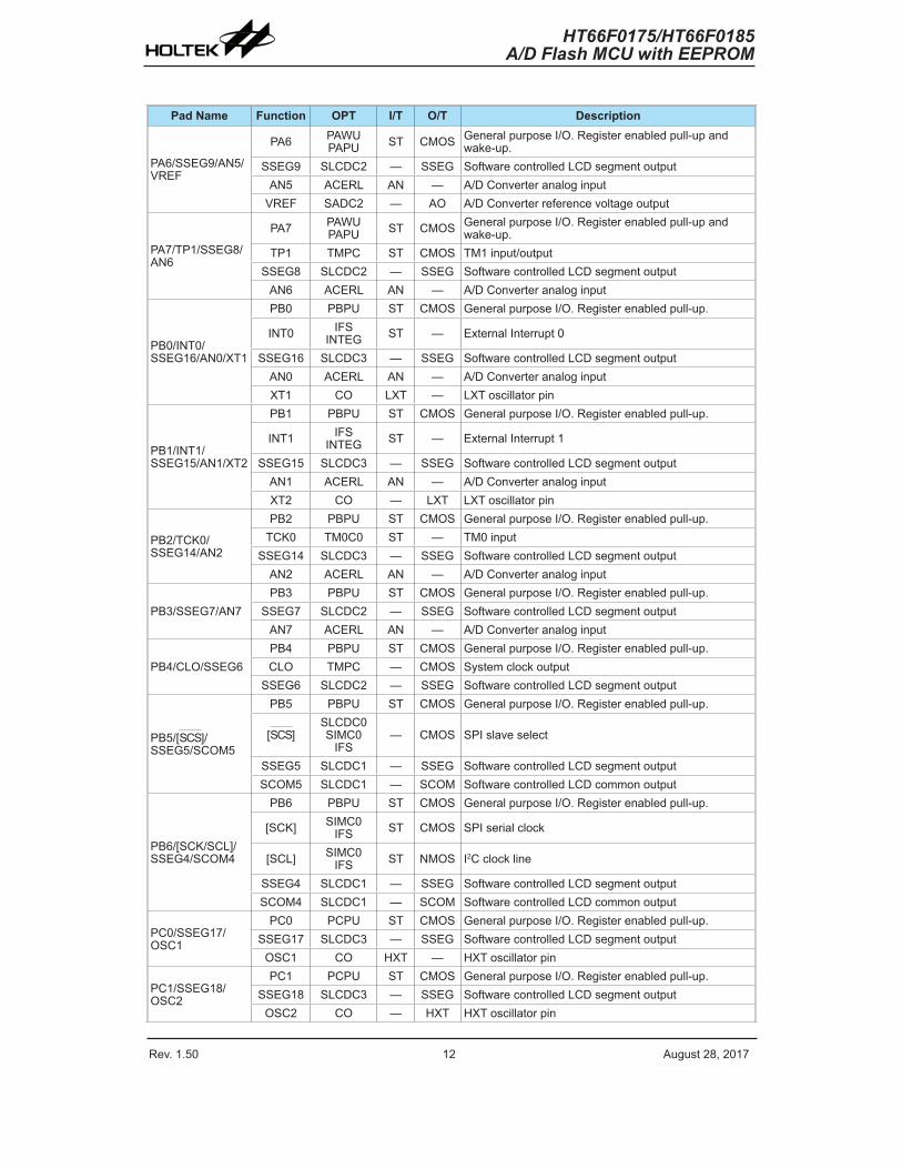
HT66F0175Pad Name Function OPT I/T O/T Description
P�0/TP0/ICPD�/OCDSD�
P�0 P�WUP�PU ST CMOS General p�rpose I/O. Re�ister enabled p�ll-�p and
wake-�p.TP0 TMPC ST CMOS TM0 inp�t/o�tp�t
ICPD� — ST CMOS ICP Data/�ddress pinOCDSD� — ST CMOS OCDS Data/�ddress pin� for EV chip only.
P�1/[SDO]/SCS/SSEG�/SCOM�
P�1 P�WUP�PU ST CMOS General p�rpose I/O. Re�ister enabled p�ll-�p and
wake-�p.
[SDO]SLCDC0SIMC0
IFS— CMOS SPI data o�tp�t
SCS SLCDC0SIMC0 IFS ST CMOS SPI slave select
SSEG� SLCDC0SLCDC1 — SSEG Software controlled LCD se�ment o�tp�t
SCOM� SLCDC0SLCDC1 — SCOM Software controlled LCD common o�tp�t
P��/ICPCK/OCDSCK
P�� P�WUP�PU ST CMOS General p�rpose I/O. Re�ister enabled p�ll-�p and
wake-�p.ICPCK — ST CMOS ICP Clock pin
OCDSCK — ST — OCDS Clock pin� for EV chip only.
P�3/[SDI/SD�]/SSEG3/SCOM3
P�3 P�WUP�PU ST CMOS General p�rpose I/O. Re�ister enabled p�ll-�p and
wake-�p.
[SDI]SLCDC0SIMC0
IFSST — SPI data inp�t
[SD�]SLCDC0SIMC0
IFSST NMOS I�C address/data line
SSEG3 SLCDC0SLCDC1 — SSEG Software controlled LCD se�ment o�tp�t
SCOM3 SLCDC0SLCDC1 — SCOM Software controlled LCD common o�tp�t
P�4/TCK1/SSEG13/�N3
P�4 P�WUP�PU ST CMOS General p�rpose I/O. Re�ister enabled p�ll-�p and
wake-�p.TCK1 TM1C0 ST — TM1 inp�t
SSEG13 SLCDC� — SSEG Software controlled LCD se�ment o�tp�t�N3 �CERL �N — �/D Converter analo� inp�t
P�5/SSEG10/�N4/VREFI
P�5 P�WUP�PU ST CMOS General p�rpose I/O. Re�ister enabled p�ll-�p and
wake-�p.SSEG10 SLCDC� — SSEG Software controlled LCD se�ment o�tp�t
�N4 �CERL �N — �/D Converter analo� inp�tVREFI S�DC� �N — �/D Converter PG� volta�e inp�t
Rev. 1.50 1� ����st ��� �01� Rev. 1.50 13 ����st ��� �01�
HT66F0175/HT66F0185A/D Flash MCU with EEPROM
HT66F0175/HT66F0185A/D Flash MCU with EEPROM
Pad Name Function OPT I/T O/T Description
P�6/SSEG9/�N5/VREF
P�6 P�WUP�PU ST CMOS General p�rpose I/O. Re�ister enabled p�ll-�p and
wake-�p.SSEG9 SLCDC� — SSEG Software controlled LCD se�ment o�tp�t
�N5 �CERL �N — �/D Converter analo� inp�tVREF S�DC� — �O �/D Converter reference volta�e o�tp�t
P��/TP1/SSEG�/�N6
P�� P�WUP�PU ST CMOS General p�rpose I/O. Re�ister enabled p�ll-�p and
wake-�p.TP1 TMPC ST CMOS TM1 inp�t/o�tp�t
SSEG� SLCDC� — SSEG Software controlled LCD se�ment o�tp�t�N6 �CERL �N — �/D Converter analo� inp�t
PB0/INT0/SSEG16/�N0/XT1
PB0 PBPU ST CMOS General p�rpose I/O. Re�ister enabled p�ll-�p.
INT0 IFSINTEG ST — External Interr�pt 0
SSEG16 SLCDC3 — SSEG Software controlled LCD se�ment o�tp�t�N0 �CERL �N — �/D Converter analo� inp�tXT1 CO LXT — LXT oscillator pin
PB1/INT1/SSEG15/�N1/XT�
PB1 PBPU ST CMOS General p�rpose I/O. Re�ister enabled p�ll-�p.
INT1 IFSINTEG ST — External Interr�pt 1
SSEG15 SLCDC3 — SSEG Software controlled LCD se�ment o�tp�t�N1 �CERL �N — �/D Converter analo� inp�tXT� CO — LXT LXT oscillator pin
PB�/TCK0/SSEG14/�N�
PB� PBPU ST CMOS General p�rpose I/O. Re�ister enabled p�ll-�p.TCK0 TM0C0 ST — TM0 inp�t
SSEG14 SLCDC3 — SSEG Software controlled LCD se�ment o�tp�t�N� �CERL �N — �/D Converter analo� inp�t
PB3/SSEG�/�N�PB3 PBPU ST CMOS General p�rpose I/O. Re�ister enabled p�ll-�p.
SSEG� SLCDC� — SSEG Software controlled LCD se�ment o�tp�t�N� �CERL �N — �/D Converter analo� inp�t
PB4/CLO/SSEG6PB4 PBPU ST CMOS General p�rpose I/O. Re�ister enabled p�ll-�p.CLO TMPC — CMOS System clock o�tp�t
SSEG6 SLCDC� — SSEG Software controlled LCD se�ment o�tp�t
PB5/[SCS]/SSEG5/SCOM5
PB5 PBPU ST CMOS General p�rpose I/O. Re�ister enabled p�ll-�p.
[SCS]SLCDC0SIMC0
IFS— CMOS SPI slave select
SSEG5 SLCDC1 — SSEG Software controlled LCD se�ment o�tp�tSCOM5 SLCDC1 — SCOM Software controlled LCD common o�tp�t
PB6/[SCK/SCL]/SSEG4/SCOM4
PB6 PBPU ST CMOS General p�rpose I/O. Re�ister enabled p�ll-�p.
[SCK] SIMC0IFS ST CMOS SPI serial clock
[SCL] SIMC0IFS ST NMOS I�C clock line
SSEG4 SLCDC1 — SSEG Software controlled LCD se�ment o�tp�tSCOM4 SLCDC1 — SCOM Software controlled LCD common o�tp�t
PC0/SSEG1�/OSC1
PC0 PCPU ST CMOS General p�rpose I/O. Re�ister enabled p�ll-�p.SSEG1� SLCDC3 — SSEG Software controlled LCD se�ment o�tp�t
OSC1 CO HXT — HXT oscillator pin
PC1/SSEG1�/OSC�
PC1 PCPU ST CMOS General p�rpose I/O. Re�ister enabled p�ll-�p.SSEG1� SLCDC3 — SSEG Software controlled LCD se�ment o�tp�t
OSC� CO — HXT HXT oscillator pin

Rev. 1.50 1� ����st ��� �01� Rev. 1.50 13 ����st ��� �01�
HT66F0175/HT66F0185A/D Flash MCU with EEPROM
HT66F0175/HT66F0185A/D Flash MCU with EEPROM
Pad Name Function OPT I/T O/T Description
PC�/SDO/SSEG0/SCOM0
PC� PCPU ST CMOS General p�rpose I/O. Re�ister enabled p�ll-�p.
SDO SIMC0IFS — CMOS SPI data o�tp�t
SSEG0 SLCDC0SLCDC1 — SSEG Software controlled LCD se�ment o�tp�t
SCOM0 SLCDC0SLCDC1 — SCOM Software controlled LCD common o�tp�t
PC3/SDI/SD�/SSEG19
PC3 PCPU ST CMOS General p�rpose I/O. Re�ister enabled p�ll-�p.
SDI SIMC0IFS ST — SPI data inp�t
SD� SIMC0IFS ST NMOS I�C data line
SSEG19 SLCDC3 — SSEG Software controlled LCD se�ment o�tp�t
PC4/SCK/SCL/SSEG1/SCOM1
PC4 PCPU ST CMOS General p�rpose I/O. Re�ister enabled p�ll-�p.
SCK SIMC0IFS ST CMOS SPI serial clock
SCL SIMC0IFS ST NMOS I�C clock line
SSEG1 SLCDC0SLCDC1 — SSEG Software controlled LCD se�ment o�tp�t
SCOM1 SLCDC0SLCDC1 — SCOM Software controlled LCD common o�tp�t
PC5/[INT1]/SSEG11
PC5 PCPU ST CMOS General p�rpose I/O. Re�ister enabled p�ll-�p.
[INT1] INTEGIFS ST — External Interr�pt 1
SSEG11 SLCDC� — SSEG Software controlled LCD se�ment o�tp�t
PC6/[INT0]/SSEG1�
PC6 PCPU ST CMOS General p�rpose I/O. Re�ister enabled p�ll-�p.
[INT0] INTEGIFS ST — External Interr�pt 0
SSEG1� SLCDC� — SSEG Software controlled LCD se�ment o�tp�t
VDD&�VDDVDD — PWR — Positive power s�pply
�VDD — PWR — �/D converter positive power s�pply
VSS&�VSSVSS — PWR — Ne�ative power s�pply� �ro�nd.
�VSS — PWR — �/D converter ne�ative power s�pply� �ro�nd.
Note:I/T:Inputtype; O/T:Outputtype;OPT:Optionalbyconfigurationoption(CO)orregisteroption;CO:Configurationoption; ST:SchmittTriggerinput; AN:Analoginput;CMOS:CMOSoutput; NMOS:NMOSoutput; AO:Analogoutput;SSEG:SoftwarecontrolledLCDSEG; SCOM:SoftwarecontrolledLCDCOM;HXT:Highfrequencycrystaloscillator; LXT:LowfrequencycrystaloscillatorPWR:Power*TheAVDDpinisinternallybondedtogetherwiththeVDDpinwhiletheAVSSpinisinternallybondedtogetherwiththeVSSpin.
AsthePinDescriptionSummarytableappliestothepackagetypewiththemostpins,notalloftheabovelistedpinsmaybepresentonpackagetypeswithsmallernumbersofpins.
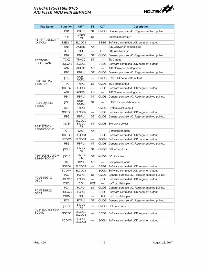
HT66F0185Pad Name Function OPT I/T O/T Description
P�0/TP0/ICPD�/OCDSD�
P�0 P�WUP�PU ST CMOS General p�rpose I/O. Re�ister enabled p�ll-�p and
wake-�p.TP0 TMPC ST CMOS TM0 inp�t/o�tp�t
ICPD� — ST CMOS ICP Data/�ddress pinOCDSD� — ST CMOS OCDS Data/�ddress pin� for EV chip only.

Rev. 1.50 14 ����st ��� �01� Rev. 1.50 15 ����st ��� �01�
HT66F0175/HT66F0185A/D Flash MCU with EEPROM
HT66F0175/HT66F0185A/D Flash MCU with EEPROM
Pad Name Function OPT I/T O/T Description
P�1/[SDO]/SSEG�/SCOM�
P�1 P�WUP�PU ST CMOS General p�rpose I/O. Re�ister enabled p�ll-�p and
wake-�p.
[SDO]SLCDC0SIMC0
IFS— CMOS SPI data o�tp�t
SSEG� SLCDC0SLCDC1 — SSEG Software controlled LCD se�ment o�tp�t
SCOM� SLCDC0SLCDC1 — SCOM Software controlled LCD common o�tp�t
P��/ICPCK/OCDSCK
P�� P�WUP�PU ST CMOS General p�rpose I/O. Re�ister enabled p�ll-�p and
wake-�p.ICPCK — ST CMOS ICP Clock pin
OCDSCK — ST — OCDS Clock pin� for EV chip only.
P�3/[SDI/SD�]/CX/SSEG3/SCOM3
P�3 P�WUP�PU ST CMOS General p�rpose I/O. Re�ister enabled p�ll-�p and
wake-�p.
[SDI]SLCDC0SIMC0
IFSST — SPI data inp�t
[SD�]SLCDC0SIMC0
IFSST NMOS I�C address/data line
CX CPC — CMOS Comparator o�tp�t
SSEG3 SLCDC0SLCDC1 — SSEG Software controlled LCD se�ment o�tp�t
SCOM3 SLCDC0SLCDC1 — SCOM Software controlled LCD common o�tp�t
P�4/TCK1/SSEG15/�N3
P�4 P�WUP�PU ST CMOS General p�rpose I/O. Re�ister enabled p�ll-�p and
wake-�p.TCK1 TM1C0 ST — TM1 inp�t
SSEG15 SLCDC3 — SSEG Software controlled LCD se�ment o�tp�t�N3 �CERL �N — �/D Converter analo� inp�t
P�5/SSEG10/�N4/VREFI
P�5 P�WUP�PU ST CMOS General p�rpose I/O. Re�ister enabled p�ll-�p and
wake-�p.SSEG10 SLCDC� — SSEG Software controlled LCD se�ment o�tp�t
�N4 �CERL �N — �/D Converter analo� inp�tVREFI S�DC� �N — �/D Converter PG� volta�e inp�t
P�6/TCK�/SSEG9/�N5/VREF
P�6 P�WUP�PU ST CMOS General p�rpose I/O. Re�ister enabled p�ll-�p and
wake-�p.TCK� TM�C0 ST — TM� inp�t
SSEG9 SLCDC� — SSEG Software controlled LCD se�ment o�tp�t�N5 �CERL �N — �/D Converter analo� inp�t
VREF S�DC� — �O �/D Converter reference volta�e o�tp�t
P��/TP1/SSEG�/�N6
P�� P�WUP�PU ST CMOS General p�rpose I/O. Re�ister enabled p�ll-�p and
wake-�p.TP1 TMPC ST CMOS TM1 inp�t/o�tp�t
SSEG� SLCDC� — SSEG Software controlled LCD se�ment o�tp�t�N6 �CERL �N — �/D Converter analo� inp�t
PB0/INT0/SSEG1�/�N0/XT1
PB0 PBPU ST CMOS General p�rpose I/O. Re�ister enabled p�ll-�p.
INT0 INTEGIFS ST — External Interr�pt 0
SSEG1� SLCDC3 — SSEG Software controlled LCD se�ment o�tp�t�N0 �CERL �N — �/D Converter analo� inp�tXT1 CO LXT — LXT oscillator pin
Rev. 1.50 14 ����st ��� �01� Rev. 1.50 15 ����st ��� �01�
HT66F0175/HT66F0185A/D Flash MCU with EEPROM
HT66F0175/HT66F0185A/D Flash MCU with EEPROM
Pad Name Function OPT I/T O/T Description
PB1/INT1/SSEG1�/�N1/XT�
PB1 PBPU ST CMOS General p�rpose I/O. Re�ister enabled p�ll-�p.
INT1 INTEGIFS ST — External Interr�pt 1
SSEG1� SLCDC3 — SSEG Software controlled LCD se�ment o�tp�t�N1 �CERL �N — �/D Converter analo� inp�tXT� CO — LXT LXT oscillator pin
PB�/TCK0/SSEG16/�N�
PB� PBPU ST CMOS General p�rpose I/O. Re�ister enabled p�ll-�p.TCK0 TM0C0 ST — TM0 inp�t
SSEG16 SLCDC3 — SSEG Software controlled LCD se�ment o�tp�t�N� �CERL �N — �/D Converter analo� inp�t
PB3/[TX]/TP�/SSEG�/�N�
PB3 PBPU ST CMOS General p�rpose I/O. Re�ister enabled p�ll-�p.
[TX] UCR1UCR� — CMOS U�RT TX serial data o�tp�t
TP� TMPC ST CMOS TM� inp�t/o�tp�tSSEG� SLCDC� — SSEG Software controlled LCD se�ment o�tp�t
�N� �CERL �N — �/D Converter analo� inp�t
PB4/[RX]/CLO/SSEG6
PB4 PBPU ST CMOS General p�rpose I/O. Re�ister enabled p�ll-�p.
[RX] UCR1UCR� ST — U�RT RX serial data inp�t
CLO TMPC — CMOS System clock o�tp�tSSEG6 SLCDC� — SSEG Software controlled LCD se�ment o�tp�t
PB5/[SCS]/C-/SSEG5/SCOM5
PB5 PBPU ST CMOS General p�rpose I/O. Re�ister enabled p�ll-�p.
[SCS]SLCDC0SIMC0
IFSST CMOS SPI slave select
C- CPC �N — Comparator inp�tSSEG5 SLCDC1 — SSEG Software controlled LCD se�ment o�tp�tSCOM5 SLCDC1 — SCOM Software controlled LCD common o�tp�t
PB6/[SCK/SCL]/C+/SSEG4/SCOM4
PB6 PBPU ST CMOS General p�rpose I/O. Re�ister enabled p�ll-�p.
[SCK] SIMC0IFS ST CMOS SPI serial clock
[SCL] SIMC0IFS ST NMOS I�C clock line
C+ CPC �N — Comparator inp�tSSEG4 SLCDC1 — SSEG Software controlled LCD se�ment o�tp�tSCOM4 SLCDC1 — SCOM Software controlled LCD common o�tp�t
PC0/SSEG19/OSC1
PC0 PCPU ST CMOS General p�rpose I/O. Re�ister enabled p�ll-�p.SSEG19 SLCDC3 — SSEG Software controlled LCD se�ment o�tp�t
OSC1 CO HXT — HXT oscillator pin
PC1/SSEG�0/OSC�
PC1 PCPU ST CMOS General p�rpose I/O. Re�ister enabled p�ll-�p.SSEG�0 SLCDC3 — SSEG Software controlled LCD se�ment o�tp�t
OSC� CO — HXT HXT oscillator pin
PC�/[SDO]/SSEG0/SCOM0
PC� PCPU ST CMOS General p�rpose I/O. Re�ister enabled p�ll-�p.
[SDO] SIMC0IFS — CMOS SPI data o�tp�t
SSEG0 SLCDC0SLCDC1 — SSEG Software controlled LCD se�ment o�tp�t
SCOM0 SLCDC0SLCDC1 — SCOM Software controlled LCD common o�tp�t

Rev. 1.50 16 ����st ��� �01� Rev. 1.50 1� ����st ��� �01�
HT66F0175/HT66F0185A/D Flash MCU with EEPROM
HT66F0175/HT66F0185A/D Flash MCU with EEPROM
Pad Name Function OPT I/T O/T Description
PC3/SDO/SSEG�1
PC3 PCPU ST CMOS General p�rpose I/O. Re�ister enabled p�ll-�p.
SDO SIMC0IFS — CMOS SPI data o�tp�t
SSEG�1 SLCDC3 — SSEG Software controlled LCD se�ment o�tp�t
PC4/SDI/SD�//SSEG��
PC4 PCPU ST CMOS General p�rpose I/O. Re�ister enabled p�ll-�p.
SDI SIMC0IFS ST — SPI data inp�t
SD� SIMC0IFS ST NMOS I�C data line
SSEG�� SLCDC4 — SSEG Software controlled LCD se�ment o�tp�t
PC5/SCK/SCL/SSEG1/SCOM1
PC5 PCPU ST CMOS General p�rpose I/O. Re�ister enabled p�ll-�p.
SCK SIMC0IFS ST CMOS SPI serial clock
SCL SIMC0IFS ST NMOS I�C clock line
SSEG1 SLCDC0SLCDC1 — SSEG Software controlled LCD se�ment o�tp�t
SCOM1 SLCDC0SLCDC1 — SCOM Software controlled LCD common o�tp�t
PC6/SCS/SSEG�3
PC6 PCPU ST CMOS General p�rpose I/O. Re�ister enabled p�ll-�p.
SCS SLCDC0SIMC0 IFS ST CMOS SPI slave select
SSEG�3 SLCDC4 — SSEG Software controlled LCD se�ment o�tp�t
PD0/SSEG11PD0 PDPU ST CMOS General p�rpose I/O. Re�ister enabled p�ll-�p.
SSEG11 SLCDC� — SSEG Software controlled LCD se�ment o�tp�t
PD1/RX/SSEG1�
PD1 PDPU ST CMOS General p�rpose I/O. Re�ister enabled p�ll-�p.
RX UCR1UCR� ST — U�RT RX serial data inp�t
SSEG1� SLCDC� — SSEG Software controlled LCD se�ment o�tp�t
PD�/TX/SSEG13
PD� PDPU ST CMOS General p�rpose I/O. Re�ister enabled p�ll-�p.
TX UCR1UCR� — CMOS U�RT TX serial data o�tp�t
SSEG13 SLCDC� — SSEG Software controlled LCD se�ment o�tp�t
PD3/SSEG14PD3 PDPU ST CMOS General p�rpose I/O. Re�ister enabled p�ll-�p.
SSEG14 SLCDC3 — SSEG Software controlled LCD se�ment o�tp�t
VDD&�VDDVDD — PWR — Positive power s�pply
�VDD — PWR — �/D converter positive power s�pply
VSS&�VSSVSS — PWR — Ne�ative power s�pply� �ro�nd.
�VSS — PWR — �/D converter ne�ative power s�pply� �ro�nd.
Note:I/T:Inputtype; O/T:Outputtype;OPT:Optionalbyconfigurationoption(CO)orregisteroption;CO:Configurationoption; ST:SchmittTriggerinput; AN:Analoginput;CMOS:CMOSoutput; NMOS:NMOSoutput; AO:Analogoutput;SSEG:SoftwarecontrolledLCDSEG; SCOM:SoftwarecontrolledLCDCOM;HXT:Highfrequencycrystaloscillator; LXT:LowfrequencycrystaloscillatorPWR:Power*TheAVDDpinisinternallybondedtogetherwiththeVDDpinwhiletheAVSSpinisinternallybondedtogetherwiththeVSSpin.
AsthePinDescriptionSummarytableappliestothepackagetypewiththemostpins,notalloftheabovelistedpinsmaybepresentonpackagetypeswithsmallernumbersofpins.

Rev. 1.50 16 ����st ��� �01� Rev. 1.50 1� ����st ��� �01�
HT66F0175/HT66F0185A/D Flash MCU with EEPROM
HT66F0175/HT66F0185A/D Flash MCU with EEPROM
Absolute Maximum RatingsSupplyVoltage..................................................................................................VSS−0.3VtoVSS+6.0VInputVoltage.....................................................................................................VSS−0.3VtoVDD+0.3VStorageTemperature...................................................................................................... -50˚Cto125˚COperatingTemperature.....................................................................................................-40˚Cto85˚CIOHTotal.......................................................................................................................................-80mAIOLTotal........................................................................................................................................80mATotalPowerDissipation........................................................................................................... 500mW
Note:Theseare stress ratingsonly.Stressesexceeding the range specifiedunder “AbsoluteMaximumRatings”maycausesubstantialdamagetothesedevices.Functionaloperationofthesedevicesatotherconditionsbeyondthoselistedinthespecificationisnot impliedandprolongedexposuretoextremeconditionsmayaffectdevicesreliability.
D.C. CharacteristicsTa=�5°C
Symbol ParameterTest Conditions
Min. Typ. Max. UnitVDD Conditions
VDD
Operatin� Volta�e (HXT) —
fSYS= fHXT=�MHz �.� — 5.5 VfSYS= fHXT=1�MHz �.� — 5.5 VfSYS= fHXT=16MHz 4.5 — 5.5 VfSYS= fHXT=�0MHz 4.5 — 5.5 V
Operatin� Volta�e (HIRC) —fSYS= fHIRC=�MHz �.� — 5.5 VfSYS= fHIRC=1�MHz �.� — 5.5 VfSYS= fHIRC=16MHz 4.5 — 5.5 V
IDD
Operatin� C�rrent (HXT)
3V fSYS=fH= fHXT=�MHzNo load� all peripherals off
— 1.0 1.5 m�5V — �.5 4.0 m�3V fSYS=fH= fHXT=1�MHz
No load� all peripherals off— 1.5 �.5 m�
5V — 3.5 5.5 m�
5V fSYS=fH= fHXT=16MHz� no load� all peripherals off — 4.5 �.0 m�
5V fSYS=fH= fHXT=�0MHz� no load� all peripherals off — 5.5 �.5 m�
Operatin� C�rrent (HIRC)
3V fSYS=fH= fHIRC=�MHzNo load� all peripherals off
— �.0 �.� m�5V — 3.0 4.5 m�3V fSYS=fH= fHIRC=1�MHz
No load� all peripherals off— 3.0 4.� m�
5V — 4.5 6.� m�
5V fSYS=fH= fHIRC=16MHzNo load� all peripherals off — 6.0 9.0 m�
Operatin� C�rrent (LXT)3V fSYS=fSUB=fLXT=3�.�6�kHz
No load� all peripherals off— 10 �0 μA
5V — 30 50 μA
Operatin� C�rrent (LIRC)3V fSYS=fSUB=fLIRC=3�kHz
No load� all peripherals off— 10 �0 μA
5V — 30 50 μA

Rev. 1.50 1� ����st ��� �01� Rev. 1.50 19 ����st ��� �01�
HT66F0175/HT66F0185A/D Flash MCU with EEPROM
HT66F0175/HT66F0185A/D Flash MCU with EEPROM
Symbol ParameterTest Conditions
Min. Typ. Max. UnitVDD Conditions
ISTB
Standby C�rrent (IDLE0 Mode)3V No load� all peripherals off�
fSUB on— 3 5 μA
5V — 5 10 μA
Standby C�rrent (IDLE1 Mode)
3V fSYS=fHXT=�MHz on� fSUB onNo load� all peripherals off
— 0.5 1.0 m�5V — 1.0 �.0 m�3V fSYS=fHXT=1�MHz on� fSUB on
No load� all peripherals off— 0.6 1.� m�
5V — 1.� �.4 m�
5V fSYS=fHXT=16MHz on� fSUB onNo load� all peripherals off — �.0 4.0 m�
5V fSYS=fHXT=�0MHz on� fSUB onNo load� all peripherals off — �.5 5.0 m�
3V fSYS=fHIRC=�MHz on� fSUB onNo load� all peripherals off
— 0.� 1.6 m�5V — 1.0 �.0 m�3V fSYS=fHIRC=1�MHz on� fSUB on
No load� all peripherals off— 1.� �.4 m�
5V — 1.5 3.0 m�
5V fSYS=fHIRC=16MHz on� fSUB onNo load� all peripherals off — �.0 4.0 m�
Standby C�rrent (SLEEP0 Mode)3V fSUB off� WDT disable
No load� all peripherals off— — 1.0 μA
5V — — �.0 μA
Standby C�rrent (SLEEP1 Mode)3V fSUB on� WDT enable
No load� all peripherals off— — 3.0 μA
5V — — 5.0 μA
VILInp�t Low Volta�e for I/O Ports or Inp�t Pins
5V — 0 — 1.5 V— — 0 — 0.�VDD V
VIHInp�t Hi�h Volta�e for I/O Ports or Inp�t Pins
5V — 3.5 — 5.0 V— — 0.�VDD — VDD V
IOL Sink C�rrent for I/O Port3V VOL = 0.1VDD 16 3� — m�5V VOL = 0.1VDD 3� 64 — m�
IOH So�rce C�rrent for I/O Port
3V VOH = 0.9VDD� SLEDCn [m+1� m] = 00n = 0 or 1; m = 0� �� 4 or 6
-1.0 -�.0 — m�
5V -�.0 -4.0 — m�
3V VOH = 0.9VDD� SLEDCn [m+1� m] = 01n = 0 or 1; m = 0� �� 4 or 6
-1.�5 -3.5 — m�
5V -3.5 -�.0 — m�
3V VOH = 0.9VDD� SLEDCn [m+1� m] = 10n = 0 or 1; m = 0� �� 4 or 6
-�.5 -5.0 — m�
5V -5.0 -10.0 — m�
3V VOH = 0.9VDD� SLEDCn [m+1� m] = 11n = 0 or 1; m = 0� �� 4 or 6
-5.5 -11.0 — m�
5V -11.0 -��.0 — m�
RPH P�ll-hi�h Resistance for I/O Ports3V — �0 60 100 kΩ5V — 10 30 50 kΩ

Rev. 1.50 1� ����st ��� �01� Rev. 1.50 19 ����st ��� �01�
HT66F0175/HT66F0185A/D Flash MCU with EEPROM
HT66F0175/HT66F0185A/D Flash MCU with EEPROM
A.C. CharacteristicsTa=�5°C
Symbol ParameterTest Condition
Min. Typ. Max. UnitVDD Condition
fSYS
System Clock (HXT)
�.�V~5.5V fSYS=fHXT=�MHz — � — MHz�.�V~5.5V fSYS=fHXT=1�MHz — 1� — MHz4.5V~5.5V fSYS=fHXT=16MHz — 16 — MHz4.5V~5.5V fSYS=fHXT=�0MHz — �0 — MHz
System Clock (HIRC)�.4V~5.5V fSYS=fHIRC=�MHz — � — MHz�.�V~5.5V fSYS=fHIRC=1�MHz — 1� — MHz4.5V~5.5V fSYS=fHIRC=16MHz — 16 — MHz
System Clock (LXT) �.�V~5.5V fSYS=fLXT=3�.�6�kHz — 3�.�6� — kHzSystem Clock (LIRC) �.�V~5.5V fSYS=fLIRC=3�kHz — 3� — kHz
fLIRC Low Speed Internal RC oscillator (LIRC)5V Ta=�5°C -10% 3� +10% kHz
�.�V~5.5V Ta=-40°C to �5°C -50% 3� +60% kHz
tTCK TCKn pin Minim�m Inp�t P�lse Width — — 0.3 — — μs
tINT Interr�pt Pin Minim�m Inp�t P�lse Width — — 10 — — μs
tSST
System Start-�p Timer Period(Wake-�p from power down mode and fSYS off)
— fSYS=fHXT off 1�� — — tHXT
— fSYS=fHIRC off 16 — — tHIRC
— fSYS=fLXT off 1�� — — tLXT
— fSYS=fLIRC off � — — tLIRC
System Start-�p Timer Period(Wake-�p from power down mode) — fSYS on � — — tSYS
tRSTD
System reset delay time(Power-on reset� LVR hardware reset� LVRC/WDTC software reset)
— — �5 50 100 ms
System reset delay time(WDT hardware reset) — — �.3 16.� 33.3 ms
tEERD EEPROM Read Time — — — — 4 tSYS
tEEWR EEPROM Write Time — — — � 4 ms
Note:tSYS=1/fSYS
Rev. 1.50 �0 ����st ��� �01� Rev. 1.50 �1 ����st ��� �01�
HT66F0175/HT66F0185A/D Flash MCU with EEPROM
HT66F0175/HT66F0185A/D Flash MCU with EEPROM
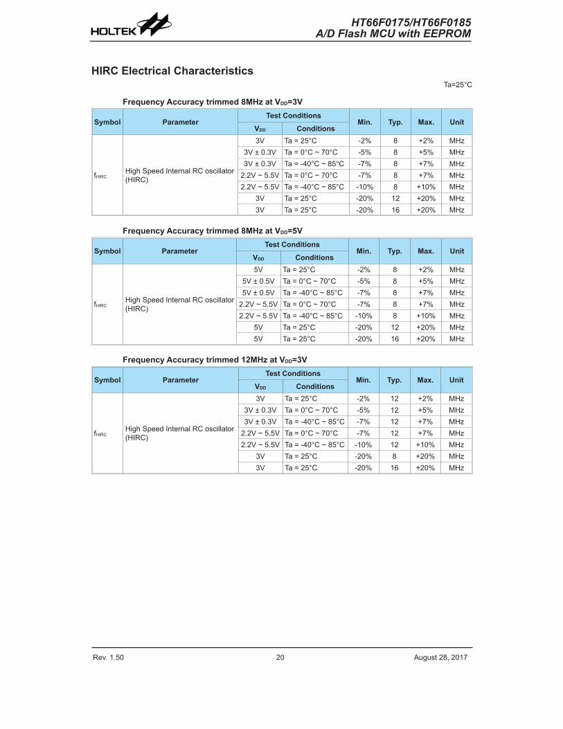
HIRC Electrical CharacteristicsTa=�5°C
Frequency Accuracy trimmed 8MHz at VDD=3V
Symbol ParameterTest Conditions
Min. Typ. Max. UnitVDD Conditions
fHIRCHi�h Speed Internal RC oscillator (HIRC)
3V Ta = �5°C -�% � +�% MHz3V ± 0.3V Ta = 0°C ~ �0°C -5% � +5% MHz3V ± 0.3V Ta = -40°C ~ �5°C -�% � +�% MHz
�.�V ~ 5.5V Ta = 0°C ~ �0°C -�% � +�% MHz�.�V ~ 5.5V Ta = -40°C ~ �5°C -10% � +10% MHz
3V Ta = �5°C -�0% 1� +�0% MHz3V Ta = �5°C -�0% 16 +�0% MHz
Frequency Accuracy trimmed 8MHz at VDD=5V
Symbol ParameterTest Conditions
Min. Typ. Max. UnitVDD Conditions
fHIRCHi�h Speed Internal RC oscillator (HIRC)
5V Ta = �5°C -�% � +�% MHz5V ± 0.5V Ta = 0°C ~ �0°C -5% � +5% MHz5V ± 0.5V Ta = -40°C ~ �5°C -�% � +�% MHz
�.�V ~ 5.5V Ta = 0°C ~ �0°C -�% � +�% MHz�.�V ~ 5.5V Ta = -40°C ~ �5°C -10% � +10% MHz
5V Ta = �5°C -�0% 1� +�0% MHz5V Ta = �5°C -�0% 16 +�0% MHz
Frequency Accuracy trimmed 12MHz at VDD=3V
Symbol ParameterTest Conditions
Min. Typ. Max. UnitVDD Conditions
fHIRCHi�h Speed Internal RC oscillator (HIRC)
3V Ta = �5°C -�% 1� +�% MHz3V ± 0.3V Ta = 0°C ~ �0°C -5% 1� +5% MHz3V ± 0.3V Ta = -40°C ~ �5°C -�% 1� +�% MHz
�.�V ~ 5.5V Ta = 0°C ~ �0°C -�% 1� +�% MHz�.�V ~ 5.5V Ta = -40°C ~ �5°C -10% 1� +10% MHz
3V Ta = �5°C -�0% � +�0% MHz3V Ta = �5°C -�0% 16 +�0% MHz

Rev. 1.50 �0 ����st ��� �01� Rev. 1.50 �1 ����st ��� �01�
HT66F0175/HT66F0185A/D Flash MCU with EEPROM
HT66F0175/HT66F0185A/D Flash MCU with EEPROM
Frequency Accuracy trimmed 12MHz at VDD=5V
Symbol ParameterTest Conditions
Min. Typ. Max. UnitVDD Conditions
fHIRCHi�h Speed Internal RC oscillator (HIRC)
5V Ta = �5°C -�% 1� +�% MHz5V ± 0.5V Ta = 0°C ~ �0°C -5% 1� +5% MHz5V ± 0.5V Ta = -40°C ~ �5°C -�% 1� +�% MHz
�.�V ~ 5.5V Ta = 0°C ~ �0°C -�% 1� +�% MHz�.�V ~ 5.5V Ta = -40°C ~ �5°C -10% 1� +10% MHz
5V Ta = �5°C -�0% � +�0% MHz5V Ta = �5°C -�0% 16 +�0% MHz
Frequency Accuracy trimmed 16MHz at VDD=5V
Symbol ParameterTest Conditions
Min. Typ. Max. UnitVDD Conditions
fHIRCHi�h Speed Internal RC oscillator (HIRC)
5V Ta = �5°C -�% 16 +�% MHz5V ± 0.5V Ta = 0°C ~ �0°C -5% 16 +5% MHz5V ± 0.5V Ta = -40°C ~ �5°C -�% 16 +�% MHz
�.�V ~ 5.5V Ta = 0°C ~ �0°C -�% 16 +�% MHz�.�V ~ 5.5V Ta = -40°C ~ �5°C -10% 16 +10% MHz
5V Ta = �5°C -�0% � +�0% MHz5V Ta = �5°C -�0% 1� +�0% MHz
A/D Converter Electrical CharacteristicsTa=�5°C
Symbol ParameterTest Conditions
Min. Typ. Max. UnitVDD Conditions
VDD Operatin� Volta�e — — �.� — 5.5 VV�DI Inp�t Volta�e — — 0 — VR\EF VVREF Reference Volta�e — — � — VDD V
DNL Differential non-linearity�.�V~�.�V VREF=VDD� t�DCK=8μs — ±15 — LSB�.�V~5.5V VREF=VDD� t�DCK=0.5μs -3 — +3 LSB
INL Inte�ral non-linearity�.�V~�.�V VREF=VDD� t�DCK=8μs — ±16 — LSB�.�V~5.5V VREF=VDD� t�DCK=0.5μs -4 — +4 LSB
I�DC�dditional C�rrent Cons�mption for �/D Converter Enable
3VNo load� t�DCK=0.5μs
— 1.0 �.0 m�5V — 1.5 3.0 m�
t�DCK Clock Period�.�V~�.�V — � — 10 μs�.�V~5.5V — 0.5 — 10 μs
t�DCConversion Time (�/D Sample and Hold Time) — — — 16 — t�DCK
tON�ST �/D Converter On-to-Start Time — — 4 — — μs
Rev. 1.50 �� ����st ��� �01� Rev. 1.50 �3 ����st ��� �01�
HT66F0175/HT66F0185A/D Flash MCU with EEPROM
HT66F0175/HT66F0185A/D Flash MCU with EEPROM
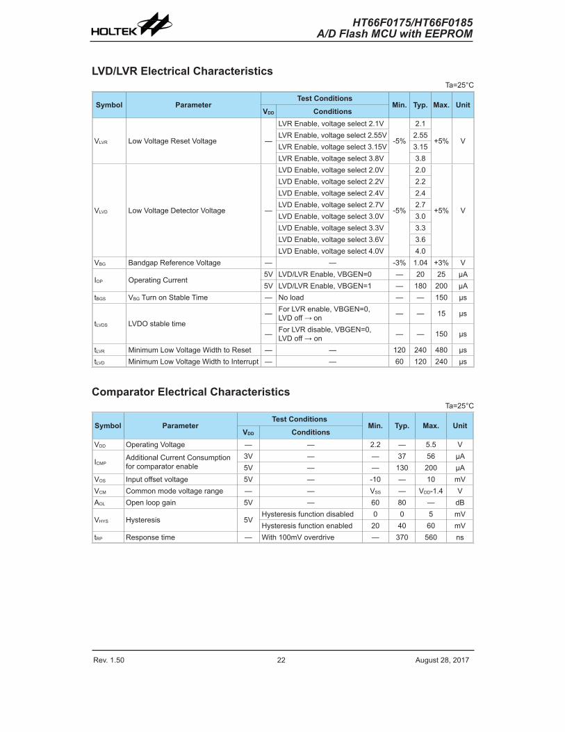
LVD/LVR Electrical CharacteristicsTa=�5°C
Symbol ParameterTest Conditions
Min. Typ. Max. UnitVDD Conditions
VLVR Low Volta�e Reset Volta�e —
LVR Enable� volta�e select �.1V
-5%
�.1
+5% VLVR Enable� volta�e select �.55V �.55LVR Enable� volta�e select 3.15V 3.15LVR Enable� volta�e select 3.�V 3.�
VLVD Low Volta�e Detector Volta�e —
LVD Enable� volta�e select �.0V
-5%
�.0
+5% V
LVD Enable� volta�e select �.�V �.�LVD Enable� volta�e select �.4V �.4LVD Enable� volta�e select �.�V �.�LVD Enable� volta�e select 3.0V 3.0LVD Enable� volta�e select 3.3V 3.3LVD Enable� volta�e select 3.6V 3.6LVD Enable� volta�e select 4.0V 4.0
VBG Band�ap Reference Volta�e — — -3% 1.04 +3% V
IOP Operatin� C�rrent5V LVD/LVR Enable� VBGEN=0 — �0 �5 μA5V LVD/LVR Enable� VBGEN=1 — 1�0 �00 μA
tBGS VBG T�rn on Stable Time — No load — — 150 μs
tLVDS LVDO stable time— For LVR enable� VBGEN=0�
LVD off →on — — 15 μs
— For LVR disable� VBGEN=0�LVD off → on — — 150 μs
tLVR Minim�m Low Volta�e Width to Reset — — 1�0 �40 4�0 μstLVD Minim�m Low Volta�e Width to Interr�pt — — 60 1�0 �40 μs
Comparator Electrical CharacteristicsTa=�5°C
Symbol ParameterTest Conditions
Min. Typ. Max. UnitVDD Conditions
VDD Operatin� Volta�e — — �.� — 5.5 V
ICMP�dditional C�rrent Cons�mption for comparator enable
3V — — 3� 56 μA5V — — 130 �00 μA
VOS Inp�t offset volta�e 5V — -10 — 10 mVVCM Common mode volta�e ran�e — — VSS — VDD-1.4 V�OL Open loop �ain 5V — 60 �0 — dB
VHYS Hysteresis 5VHysteresis f�nction disabled 0 0 5 mVHysteresis f�nction enabled �0 40 60 mV
tRP Response time — With 100mV overdrive — 3�0 560 ns

Rev. 1.50 �� ����st ��� �01� Rev. 1.50 �3 ����st ��� �01�
HT66F0175/HT66F0185A/D Flash MCU with EEPROM
HT66F0175/HT66F0185A/D Flash MCU with EEPROM
Software Controlled LCD Driver Electrical CharacteristicsTa=�5°C
Symbol ParameterTest Conditions
Min. Typ. Max. UnitVDD Conditions
IBI�S Bias c�rrent 5V
ISEL[1:0]=00 4.� �.3 13 μAISEL[1:0]=01 �.3 16.� �5 μAISEL[1:0]=10 �5 50 �5 μAISEL[1:0]=11 50 100 150 μA
VLCD_H [(�/3) × VDD] volta�e for LCD SCOM/SSEG o�tp�t �.�V~5.5V No load 0.645 0.6� 0.69� VDD
VLCD_L [(1/3) × VDD] volta�e for LCD SCOM/SSEG o�tp�t �.�V~5.5V No load 0.305 0.33 0.355 VDD
Power-on Reset CharacteristicsTa=�5°C
Symbol ParameterTest Conditions
Min. Typ. Max. UnitVDD Conditions
VPOR VDD Start Volta�e to Ens�re Power-on Reset — — — — 100 mVRRVDD VDD Raisin� Rate to Ens�re Power-on Reset — — 0.035 — — V/ms
tPORMinim�m Time for VDD Stays at VPOR to Ens�re Power-on Reset — — 1 — — ms
� � � �
� � �
� � � �
� � � � �� � � �
Rev. 1.50 �4 ����st ��� �01� Rev. 1.50 �5 ����st ��� �01�
HT66F0175/HT66F0185A/D Flash MCU with EEPROM
HT66F0175/HT66F0185A/D Flash MCU with EEPROM
System ArchitectureAkeyfactorinthehigh-performancefeaturesoftheHoltekrangeofmicrocontrollersisattributedtotheirinternalsystemarchitecture.TherangeofdevicestakeadvantageoftheusualfeaturesfoundwithinRISCmicrocontrollersprovidingincreasedspeedofoperationandenhancedperformance.Thepipeliningscheme is implemented insuchaway that instruction fetchingand instructionexecutionareoverlapped,hence instructionsareeffectivelyexecuted inonecycle,with theexceptionofbranchorcallinstructions.An8-bitwideALUisusedinpracticallyallinstructionsetoperations,whichcarriesoutarithmeticoperations,logicoperations,rotation,increment,decrement,branchdecisions,etc.TheinternaldatapathissimplifiedbymovingdatathroughtheAccumulatorandtheALU.CertaininternalregistersareimplementedintheDataMemoryandcanbedirectlyor indirectlyaddressed.Thesimpleaddressingmethodsof theseregistersalongwithadditionalarchitectural featuresensure thataminimumofexternalcomponents is required toprovideafunctionalI/OandA/Dcontrolsystemwithmaximumreliabilityandflexibility.Thismakesthesedevicessuitableforlow-cost,high-volumeproductionforcontrollerapplications.
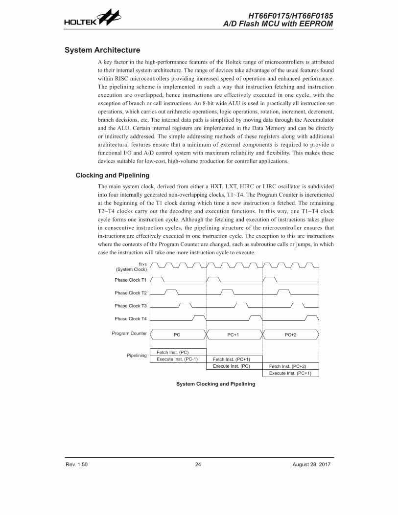
Clocking and PipeliningThemainsystemclock,derivedfromeitheraHXT,LXT,HIRCorLIRCoscillatorissubdividedintofourinternallygeneratednon-overlappingclocks,T1~T4.TheProgramCounterisincrementedat thebeginningof theT1clockduringwhichtimeanewinstruction isfetched.TheremainingT2~T4clockscarryout thedecodingandexecution functions. In thisway,oneT1~T4clockcycleformsoneinstructioncycle.Althoughthefetchingandexecutionofinstructionstakesplaceinconsecutive instructioncycles, thepipeliningstructureof themicrocontrollerensures thatinstructionsareeffectivelyexecutedinoneinstructioncycle.TheexceptiontothisareinstructionswherethecontentsoftheProgramCounterarechanged,suchassubroutinecallsorjumps,inwhichcasetheinstructionwilltakeonemoreinstructioncycletoexecute.
� � � � � � � � � � � � � � � �� � � � � � � � � � � � � � � � � � � � � � � � � � � � � � � � � � � �
� � � � � � � � � � � � � � � � � � � � � � � � � � � � � � � � � � � �� � � � � � � � � � � � � � � � � � �
� � � � � � � � �
� � � � � � � � � � � � � �
� � � � � � � � � � � � �
� � � � � � � � � � � � � � �
� � � � � � � � � � � � � �
� � � � � � � � � � � � � �
� � � � � � � � � � � � � �
� � � � � � � � � �
System Clocking and Pipelining
Rev. 1.50 �4 ����st ��� �01� Rev. 1.50 �5 ����st ��� �01�
HT66F0175/HT66F0185A/D Flash MCU with EEPROM
HT66F0175/HT66F0185A/D Flash MCU with EEPROM
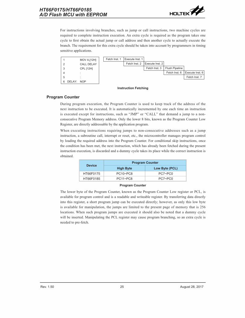
For instructions involvingbranches,suchas jumporcall instructions, twomachinecyclesarerequired tocomplete instructionexecution.Anextracycle is requiredas theprogramtakesonecycletofirstobtaintheactualjumporcalladdressandthenanothercycletoactuallyexecutethebranch.Therequirementforthisextracycleshouldbetakenintoaccountbyprogrammersintimingsensitiveapplications.
� � � � � � � � � � � � � � � � � � � � � � � � � � � �� � � � � � � � � � � � �
� � � � � � � � � � � � �
���� � � � � � �
� � � � � � � � � � �� � � � � � � � � �� � � � � � � � ���� � �
� � � � � � � � � � � � � � �� � � � � � � � � � � � �
� � � � � � � � � � � � � � � � � � � � � � � � � � � � � � � � � � � � � �
Instruction Fetching
Program CounterDuringprogramexecution, theProgramCounter isused tokeep trackof theaddressof thenext instruction tobeexecuted. It isautomatically incrementedbyoneeach timean instructionisexecutedexcept for instructions, suchas“JMP”or“CALL” thatdemanda jump toanon-consecutiveProgramMemoryaddress.Onlythelower8bits,knownastheProgramCounterLowRegister,aredirectlyaddressablebytheapplicationprogram.
Whenexecuting instructions requiring jumps tonon-consecutiveaddresses suchas a jumpinstruction,asubroutinecall, interruptorreset,etc., themicrocontrollermanagesprogramcontrolbyloadingtherequiredaddressintotheProgramCounter.Forconditionalskipinstructions,oncetheconditionhasbeenmet,thenextinstruction,whichhasalreadybeenfetchedduringthepresentinstructionexecution,isdiscardedandadummycycletakesitsplacewhilethecorrectinstructionisobtained.
DeviceProgram Counter
High Byte Low Byte (PCL)HT66F01�5 PC10~PC� PC�~PC0HT66F01�5 PC11~PC� PC�~PC0
Program Counter
Thelowerbyteof theProgramCounter,knownastheProgramCounterLowregisterorPCL,isavailableforprogramcontrolandisareadableandwriteableregister.Bytransferringdatadirectlyintothisregister,ashortprogramjumpcanbeexecuteddirectly;however,asonlythis lowbyteisavailable formanipulation, the jumpsare limited to thepresentpageofmemory that is256locations.Whensuchprogramjumpsareexecuted itshouldalsobenoted thatadummycyclewillbeinserted.ManipulatingthePCLregistermaycauseprogrambranching,soanextracycleisneededtopre-fetch.
Rev. 1.50 �6 ����st ��� �01� Rev. 1.50 �� ����st ��� �01�
HT66F0175/HT66F0185A/D Flash MCU with EEPROM
HT66F0175/HT66F0185A/D Flash MCU with EEPROM
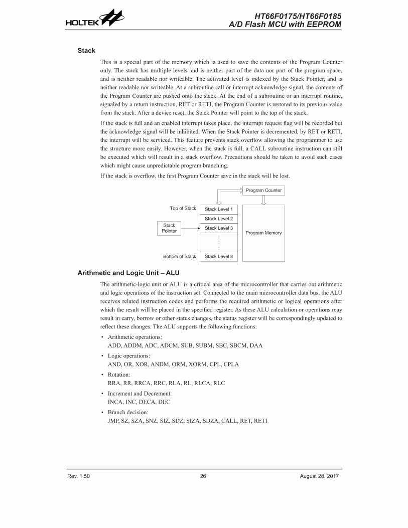
StackThis isaspecialpartof thememorywhichisusedtosavethecontentsof theProgramCounteronly.Thestackhasmultiple levelsandisneitherpartof thedatanorpartof theprogramspace,andisneitherreadablenorwriteable.Theactivatedlevel is indexedbytheStackPointer,andisneitherreadablenorwriteable.Atasubroutinecallorinterruptacknowledgesignal,thecontentsoftheProgramCounterarepushedontothestack.Attheendofasubroutineoraninterruptroutine,signaledbyareturninstruction,RETorRETI,theProgramCounterisrestoredtoitspreviousvaluefromthestack.Afteradevicereset,theStackPointerwillpointtothetopofthestack.
Ifthestackisfullandanenabledinterrupttakesplace,theinterruptrequestflagwillberecordedbuttheacknowledgesignalwillbeinhibited.WhentheStackPointerisdecremented,byRETorRETI,theinterruptwillbeserviced.Thisfeaturepreventsstackoverflowallowingtheprogrammertousethestructuremoreeasily.However,whenthestackisfull,aCALLsubroutineinstructioncanstillbeexecutedwhichwillresultinastackoverflow.Precautionsshouldbetakentoavoidsuchcaseswhichmightcauseunpredictableprogrambranching.
Ifthestackisoverflow,thefirstProgramCountersaveinthestackwillbelost.
StackPointer
Stack Level �
Stack Level 1
Stack Level 3
:::
Stack Level �
Pro�ram Memory
Pro�ram Co�nter
Bottom of Stack
Top of Stack
Arithmetic and Logic Unit – ALUThearithmetic-logicunitorALUisacriticalareaofthemicrocontrollerthatcarriesoutarithmeticandlogicoperationsoftheinstructionset.Connectedtothemainmicrocontrollerdatabus,theALUreceivesrelatedinstructioncodesandperformstherequiredarithmeticor logicaloperationsafterwhichtheresultwillbeplacedinthespecifiedregister.AstheseALUcalculationoroperationsmayresultincarry,borroworotherstatuschanges,thestatusregisterwillbecorrespondinglyupdatedtoreflectthesechanges.TheALUsupportsthefollowingfunctions:
• Arithmeticoperations:ADD,ADDM,ADC,ADCM,SUB,SUBM,SBC,SBCM,DAA
• Logicoperations:AND,OR,XOR,ANDM,ORM,XORM,CPL,CPLA
• Rotation:RRA,RR,RRCA,RRC,RLA,RL,RLCA,RLC
• IncrementandDecrement:INCA,INC,DECA,DEC
• Branchdecision:JMP,SZ,SZA,SNZ,SIZ,SDZ,SIZA,SDZA,CALL,RET,RETI
Rev. 1.50 �6 ����st ��� �01� Rev. 1.50 �� ����st ��� �01�
HT66F0175/HT66F0185A/D Flash MCU with EEPROM
HT66F0175/HT66F0185A/D Flash MCU with EEPROM
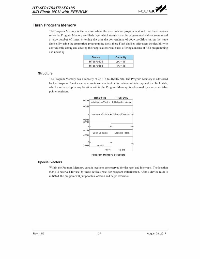
Flash Program MemoryTheProgramMemoryisthelocationwheretheusercodeorprogramisstored.ForthesedevicesseriestheProgramMemoryareFlashtype,whichmeansitcanbeprogrammedandre-programmeda largenumberof times,allowing theuser theconvenienceofcodemodificationon thesamedevice.Byusingtheappropriateprogrammingtools,theseFlashdevicesofferuserstheflexibilitytoconvenientlydebuganddeveloptheirapplicationswhilealsoofferingameansoffieldprogrammingandupdating.
Device CapacityHT66F01�5 �K × 16HT66F01�5 4K × 16
StructureTheProgramMemoryhasacapacityof2K×16to4K×16bits.TheProgramMemoryisaddressedbytheProgramCounterandalsocontainsdata,tableinformationandinterruptentries.Tabledata,whichcanbesetupinanylocationwithintheProgramMemory, isaddressedbyaseparatetablepointerregisters.
000HInitialisation Vector
004H
FFFH 16 bits
Interr�pt Vectors
0�4H
Look-�p Tablen00H
nFFH
HT66F0185
Initialisation Vector
16 bits
Interr�pt Vectors
Look-�p Table
HT66F0175
0��H
�FFH
Program Memory Structure
Special VectorsWithintheProgramMemory,certainlocationsarereservedfortheresetandinterrupts.Thelocation000Hisreservedforusebythesedevicesresetforprograminitialisation.Afteradevicereset isinitiated,theprogramwilljumptothislocationandbeginexecution.

Rev. 1.50 �� ����st ��� �01� Rev. 1.50 �9 ����st ��� �01�
HT66F0175/HT66F0185A/D Flash MCU with EEPROM
HT66F0175/HT66F0185A/D Flash MCU with EEPROM
Look-up TableAnylocationwithintheProgramMemorycanbedefinedasalook-uptablewhereprogrammerscanstorefixeddata.Tousethelook-uptable,thetablepointermustfirstbesetupbyplacingtheaddressof thelookupdatatoberetrievedinthetablepointerregister,TBLPandTBHP.Theseregistersdefinethetotaladdressofthelook-uptable.
Aftersettingupthetablepointer,thetabledatacanberetrievedfromtheProgramMemoryusingthe“TABRD[m]”or“TABRDL[m]”instructionsrespectively.Whentheinstructionisexecuted,the lowerorder tablebyte from theProgramMemorywillbe transferred to theuserdefinedDataMemoryregister[m]asspecified in the instruction.Thehigherorder tabledatabytefromtheProgramMemorywillbe transferred to theTBLHspecial register.Anyunusedbits in thistransferredhigherorderbytewillbereadas“0”.
Theaccompanyingdiagramillustratestheaddressingdataflowofthelook-uptable.
� � � � � � � � � � � � � � � � � � � � � � � � � �� � � � � � � �
� � � � � � � � � � � � � � �
� � � � � � � � � � � �
� � �
������� � � � � � � �
� � � � � � � � � � � � � �� � � � � � � � � � � �� � � � � � � � � � � �
Table Program ExampleTheaccompanyingexampleshowshowthetablepointerandtabledataisdefinedandretrievedfromthedevice.ThisexampleusesrawtabledatalocatedinthelastpagewhichisstoredthereusingtheORGstatement.ThevalueatthisORGstatementis“0F00H”whichreferstothestartaddressofthelastpagewithinthe4KProgramMemoryofthedevice.Thetablepointerlowbyteregisterissetupheretohaveaninitialvalueof“06H”.ThiswillensurethatthefirstdatareadfromthedatatablewillbeattheProgramMemoryaddress“0F06H”or6locationsafterthestartofthelastpage.NotethatthevalueforthetablepointerisreferencedtothefirstaddressofthepresentpagepointedbytheTBHPregisterifthe“TABRD[m]”instructionisbeingused.ThehighbyteofthetabledatawhichinthiscaseisequaltozerowillbetransferredtotheTBLHregisterautomaticallywhenthe“TABRD[m]instructionisexecuted.
Because theTBLHregister isaread-onlyregisterandcannotberestored,careshouldbe takentoensure itsprotection ifboth themain routineand InterruptServiceRoutineuse table readinstructions. Ifusing the tableread instructions, theInterruptServiceRoutinesmaychange thevalueoftheTBLHandsubsequentlycauseerrorsifusedagainbythemainroutine.Asaruleitisrecommendedthatsimultaneoususeofthetablereadinstructionsshouldbeavoided.However, insituationswheresimultaneoususecannotbeavoided,theinterruptsshouldbedisabledpriortotheexecutionofanymainroutinetable-readinstructions.Notethatalltablerelatedinstructionsrequiretwoinstructioncyclestocompletetheiroperation.

Rev. 1.50 �� ����st ��� �01� Rev. 1.50 �9 ����st ��� �01�
HT66F0175/HT66F0185A/D Flash MCU with EEPROM
HT66F0175/HT66F0185A/D Flash MCU with EEPROM
Table Read Program Exampletempreg1 db ? ; temporary register #1 tempreg2 db ? ; temporary register #2 :mov a,06h ; initialise low table pointer - note that this address is referenced mov tblp,a ; to the last page or the page that tbhp pointedmov a,0fh ; initialise high table pointer mov tbhp,a:tabrd tempreg1 ; transfers value in table referenced by table pointer data at program ; memory address “0F06H” transferred to tempreg1 and TBLH dec tblp ; reduce value of table pointer by one tabrd tempreg2 ; transfers value in table referenced by table pointer data at program ; memory address “0F05H” transferred to tempreg2 and TBLH in this ; example the data “1AH” is transferred to tempreg1 and data “0FH” to ; register tempreg2:org 0F00h ; sets initial address of program memory dc 00Ah, 00Bh, 00Ch, 00Dh, 00Eh, 00Fh, 01Ah, 01Bh:
In Circuit Programming – ICPTheprovisionofFlashtypeProgramMemoryprovides theuserwithameansofconvenientandeasyupgradesandmodificationstotheirprogramsonthesamedevice.
Asanadditionalconvenience,Holtekhasprovidedameansofprogrammingthemicrocontrollerin-circuitusinga4-pininterface.Thisprovidesmanufacturerswiththepossibilityofmanufacturingtheircircuitboardscompletewithaprogrammedorun-programmedmicrocontroller,and thenprogrammingorupgradingtheprogramatalaterstage.Thisenablesproductmanufacturerstoeasilykeeptheirmanufacturedproductssuppliedwiththelatestprogramreleaseswithoutremovalandre-insertionofthedevice.
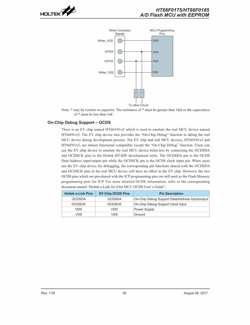
Holtek Writer Pins MCU Programming Pins Pin DescriptionICPD� P�0 Pro�rammin� Serial Data/�ddressICPCK P�� Pro�rammin� ClockVDD VDD Power S�pplyVSS VSS Gro�nd
TheProgramMemoryandEEPROMdatamemorycanbeprogrammedseriallyin-circuitusingthis4-wireinterface.Dataisdownloadedanduploadedseriallyonasinglepinwithanadditionallinefortheclock.Twoadditionallinesarerequiredforthepowersupply.Thetechnicaldetailsregardingthein-circuitprogrammingofthedevicearebeyondthescopeofthisdocumentandwillbesuppliedinsupplementaryliterature.
Duringtheprogrammingprocess,theusermusttakecareoftheICPDAandICPCKpinsfordataandclockprogrammingpurposestoensurethatnootheroutputsareconnectedtothesetwopins.
Rev. 1.50 30 ����st ��� �01� Rev. 1.50 31 ����st ��� �01�
HT66F0175/HT66F0185A/D Flash MCU with EEPROM
HT66F0175/HT66F0185A/D Flash MCU with EEPROM
� �
� � � � � � � � � �
� � � � �
� � � � �
� � � � � � � � � �
� � � � � � � � � � � � � � �
� �
� � �
� � �
� � � � � � � � � � � � � �� � � � � �
� � � � � � � � � � � � � �� � �
� � �
Note:*mayberesistororcapacitor.Theresistanceof*mustbegreaterthan1kΩorthecapacitanceof*mustbelessthan1nF.
On-Chip Debug Support – OCDSThere isanEVchipnamedHT66V01x5whichisused toemulate therealMCUdevicenamedHT66F01x5.TheEVchipdevicealsoprovidesthe“On-ChipDebug”functiontodebugtherealMCUdeviceduringdevelopmentprocess.TheEVchipandrealMCUdevices,HT66V01x5andHT66F01x5,arealmostfunctionalcompatibleexcept the“On-ChipDebug”function.Userscanuse theEVchipdevice toemulate therealMCUdevicebehaviorsbyconnecting theOCDSDAandOCDSCKpins to theHoltekHT-IDEdevelopment tools.TheOCDSDApin is theOCDSData/Addressinput/outputpinwhiletheOCDSCKpinis theOCDSclockinputpin.WhenusersusetheEVchipdevicefordebugging,thecorrespondingpinfunctionssharedwiththeOCDSDAandOCDSCKpinsintherealMCUdevicewillhavenoeffectintheEVchip.However,thetwoOCDSpinswhicharepin-sharedwiththeICPprogrammingpinsarestillusedastheFlashMemoryprogrammingpins for ICP.FormoredetailedOCDS information, refer to thecorrespondingdocumentnamed“Holteke-Linkfor8-bitMCUOCDSUser’sGuide”.
Holtek e-Link Pins EV Chip OCDS Pins Pin DescriptionOCDSD� OCDSD� On-Chip Deb�� S�pport Data/�ddress inp�t/o�tp�tOCDSCK OCDSCK On-Chip Deb�� S�pport Clock inp�t
VDD VDD Power S�pplyVSS VSS Gro�nd

Rev. 1.50 30 ����st ��� �01� Rev. 1.50 31 ����st ��� �01�
HT66F0175/HT66F0185A/D Flash MCU with EEPROM
HT66F0175/HT66F0185A/D Flash MCU with EEPROM
Data MemoryTheDataMemoryisan8-bitwideRAMinternalmemoryandis the locationwhere temporaryinformationisstored.
StructureDividedintotwobanks,thefirstoftheseisanareaofRAM,knownastheSpecialFunctionDataMemory.Herearelocatedregisterswhicharenecessaryforcorrectoperationofthedevice.Manyoftheseregisterscanbereadfromandwrittentodirectlyunderprogramcontrol,however,someremainprotectedfromusermanipulation.ThesecondareaofDataMemoryisknownastheGeneralPurposeDataMemory,whichisreservedforgeneralpurposeuse.Alllocationswithinthisareaarereadandwriteaccessibleunderprogramcontrol.
TheoverallDataMemoryissubdividedintotwobanks.TheSpecialPurposeDataMemoryregistersareaccessibleinallbanks,withtheexceptionof theEECregisterataddress40H,whichisonlyaccessibleinBank1.SwitchingbetweenthedifferentDataMemorybanksisachievedbysettingtheBankPointertothecorrectvalue.ThestartaddressoftheDataMemoryforthedeviceistheaddress00H.
TheaddressrangeoftheSpecialPurposeDataMemoryforthedeviceisfrom00Hto7FHwhiletheaddressrangeoftheGeneralPurposeDataMemoryisfrom80HtoFFH.
Device Capacity BanksHT66F01�5 1�� × � 0: �0H~FFH
HT66F01�5 �56 × � 0: �0H~FFH1: �0H~FFH
Data Memory Summary
00H
�FH�0H
FFH
Special P�rpose Data Memory
General P�rpose Data Memory
Bank 0
40H: EEC
HT66F0175
(Bank 1)
00H
�FH�0H
FFH
Special P�rpose Data Memory
General P�rpose Data Memory
Bank 0Bank 1
40H:EEC(Bank 1)
HT66F0185
Data Memory Structure

Rev. 1.50 3� ����st ��� �01� Rev. 1.50 33 ����st ��� �01�
HT66F0175/HT66F0185A/D Flash MCU with EEPROM
HT66F0175/HT66F0185A/D Flash MCU with EEPROM
00H I�R001H MP00�H I�R103H MP104H05H �CC06H PCL0�H TBLP0�H TBLH09H TBHP0�H ST�TUS0BH0CH0DH0EH0FH10H
INTC0
11H1�H
19H
P�PU
1�HP�WU
1BH1�H
1DH1CH
1FH
P�P�C
13H14H15H16H1�H
EE�
�0H�1H��H
��H
�3H�4H�5H�6H��H
40H41H4�H43H44H45H46H4�H4�H49H4�H4BH4CH4DH4EH4FH50H51H
1EH
EEC
Bank 0� 1
PBCPBPU
PB
�FH
BP
LVDC
LVRC
EEDS�DOL
S�DC0
PCCPCPU
PC
S�DOH
5�H
SMOD
INTEG
INTC1INTC�MFI0MFI1MFI�
TMPCWDTCTBC
CTRL
S�DC1S�DC�
Bank 0 Bank 1
SLEDC0SLEDC1
�CERL
SIMTOC
SIMC0SIMC1SIMD
SIM�/SIMC�
SLCDC0SLCDC1SLCDC�SLCDC3
IFS
�EH
3�H3�H
39H3�H
3CH3BH
3DH
3FH3EH
TM1C0TM1C1TM1DLTM1DHTM1�LTM1�HTM1RPLTM1RPH
�FH30H31H3�H33H34H35H
HT66F0175
TM0C0TM0C1TM0DLTM0DHTM0�LTM0�HTM0RPLTM0RPH
: Un�sed� read as 00H
36H
00H I�R001H MP00�H I�R103H MP104H05H �CC06H PCL0�H TBLP0�H TBLH09H TBHP0�H ST�TUS0BH0CH0DH0EH0FH10H
INTC0
11H1�H
19H
P�PU
1�HP�WU
1BH1�H
1DH1CH
1FH
P�P�C
13H14H15H16H1�H
EE�
�0H�1H��H
��H
�3H�4H�5H�6H��H
40H41H4�H43H44H45H46H4�H4�H49H4�H4BH4CH4DH4EH4FH50H51H
53H54H
1EH
EEC
Bank 0� 1
55H56H
PBCPBPU
PB
�FH
BP
LVDC
LVRC
EEDS�DOL
S�DC0
PCCPCPU
PC
5�H5�H59H5�H
S�DOH
5�H
SMOD
INTEG
INTC1INTC�MFI0MFI1MFI�
TMPCWDTCTBC
CTRL
S�DC1S�DC�
Bank 0 Bank 1
SLEDC0
USRUCR1UCR�
TXR_RXRBRG
SLEDC1
�CERL
SIMTOC
SIMC0SIMC1SIMD
SIM�/SIMC�
SLCDC0SLCDC1SLCDC�SLCDC3
IFS
SLCDC4
PDPDC
PDPU
TM�C0TM�C1TM�DLTM�DHTM��LTM��HTM�RP
�9H��H�BH�CH�DH�EH
3�H3�H
39H3�H
3CH3BH
3DH
3FH3EH
TM1C0TM1C1TM1DLTM1DHTM1�LTM1�H
TM1RPLTM1RPH
CPC
�FH30H31H3�H33H34H35H
HT66F0185
TM0C0TM0C1TM0DLTM0DHTM0�LTM0�HTM0RP
: Un�sed� read as 00H
36H
Special Purpose Data Memory Structure

Rev. 1.50 3� ����st ��� �01� Rev. 1.50 33 ����st ��� �01�
HT66F0175/HT66F0185A/D Flash MCU with EEPROM
HT66F0175/HT66F0185A/D Flash MCU with EEPROM
Special Function Register DescriptionMostoftheSpecialFunctionRegisterdetailswillbedescribedintherelevantfunctionalsection.However,severalregistersrequireaseparatedescriptioninthissection.
Indirect Addressing Registers – IAR0, IAR1TheIndirectAddressingRegisters,IAR0andIAR1,althoughhavingtheirlocationsinnormalRAMregisterspace,donotactuallyphysicallyexistasnormalregisters.ThemethodofindirectaddressingforRAMdatamanipulationuses theseIndirectAddressingRegistersandMemoryPointers, incontrasttodirectmemoryaddressing,wheretheactualmemoryaddressisspecified.ActionsontheIAR0andIAR1registerswillresultinnoactualreadorwriteoperationtotheseregistersbutrathertothememorylocationspecifiedbytheircorrespondingMemoryPointers,MP0orMP1.Actingasapair,IAR0andMP0cantogetheraccessdataonlyfromBank0whiletheIAR1registertogetherwithMP1registerpaircanaccessdatafromanyDataMemorybank.AstheIndirectAddressingRegistersarenotphysicallyimplemented,readingtheIndirectAddressingRegistersindirectlywillreturnaresultof“00H”andwritingtotheregistersindirectlywillresultinnooperation.
Memory Pointers – MP0, MP1TheMemoryPointers, knownasMP0andMP1, areprovided.TheseMemoryPointers arephysicallyimplementedintheDataMemoryandcanbemanipulatedinthesamewayasnormalregistersprovidingaconvenientwaywithwhichtoaddressandtrackdata.WhenanyoperationtotherelevantIndirectAddressingRegistersiscarriedout,theactualaddressthatthemicrocontrollerisdirectedtoistheaddressspecifiedbytherelatedMemoryPointer.MP0,togetherwithIndirectAddressingRegister,IAR0,areusedtoaccessdatafromBank0,whileMP1togetherwithIAR1areusedtoaccessdatafromalldatabanksaccordingtothecorrespondingBPregister.
ThefollowingexampleshowshowtoclearasectionoffourDataMemorylocationsalreadydefinedaslocationsadres1toadres4.
Indirect Addressing Program Exampledata .section ‘data’adres1 db ? adres2 db ? adres3 db ? adres4 db ? block db ? code .section at 0 ‘code’org 00h start: mov a,04h ; setup size of block mov block,a mov a,offset adres1 ; Accumulator loaded with first RAM address mov mp0,a ; setup memory pointer with first RAM address loop: clr IAR0 ; clear the data at address defined by MP0 inc mp0 ; increment memory pointer sdz block ; check if last memory location has been cleared jmp loop continue: :
Theimportantpointtonotehereisthatintheexampleshownabove,noreferenceismadetospecificRAMaddresses.

Rev. 1.50 34 ����st ��� �01� Rev. 1.50 35 ����st ��� �01�
HT66F0175/HT66F0185A/D Flash MCU with EEPROM
HT66F0175/HT66F0185A/D Flash MCU with EEPROM
Bank Pointer – BPFor theHT66F0185device, theDataMemory isdivided into twobanks,Bank0andBank1.SelectingtherequiredDataMemoryareaisachievedusingtheBankPointer.Bit0of theBankPointerisusedtoselectDataMemoryBanks0~1.TheDataMemoryisinitialisedtoBank0afterareset,exceptforaWDTtime-outresetinthePowerDownMode,inwhichcase,theDataMemorybankremainsunaffected.ItshouldbenotedthattheSpecialFunctionDataMemoryisnotaffectedby thebankselection,whichmeans that theSpecialFunctionRegisterscanbeaccessed fromwithinanybank.DirectlyaddressingtheDataMemorywillalwaysresultinBank0beingaccessedirrespectiveof thevalueof theBankPointer.AccessingdatafromBank1mustbe implementedusingIndirectAddressing.
BP Register – HT66F0185
Bit 7 6 5 4 3 2 1 0Name — — — — — — — DMBP0R/W — — — — — — — R/WPOR — — — — — — — 0
Bit7~1 Unimplemented,readas“0”Bit0 DMBP0:SelectDataMemoryBanks
0:Bank01:Bank1
Accumulator – ACCTheAccumulator iscentral to theoperationofanymicrocontrollerand isclosely relatedwithoperationscarriedoutby theALU.TheAccumulator is theplacewhereall intermediateresultsfromtheALUarestored.Without theAccumulator itwouldbenecessary towrite theresultofeachcalculationorlogicaloperationsuchasaddition,subtraction,shift,etc., totheDataMemoryresultinginhigherprogrammingandtimingoverheads.Data transferoperationsusually involvethetemporarystoragefunctionoftheAccumulator;forexample,whentransferringdatabetweenoneuserdefinedregisterandanother, it isnecessary todo thisbypassingthedata throughtheAccumulatorasnodirecttransferbetweentworegistersispermitted.
Program Counter Low Register – PCLToprovideadditionalprogramcontrolfunctions, the lowbyteof theProgramCounter ismadeaccessibletoprogrammersbylocatingitwithintheSpecialPurposeareaoftheDataMemory.Bymanipulatingthisregister,directjumpstootherprogramlocationsareeasilyimplemented.LoadingavaluedirectlyintothisPCLregisterwillcauseajumptothespecifiedProgramMemorylocation,however,astheregisterisonly8-bitwide,onlyjumpswithinthecurrentProgramMemorypagearepermitted.Whensuchoperationsareused,notethatadummycyclewillbeinserted.
Look-up Table Registers – TBLP, TBHP, TBLHThesethreespecialfunctionregistersareusedtocontroloperationof thelook-uptablewhichisstoredintheProgramMemory.TBLPandTBHParethetablepointerandindicates thelocationwhere the tabledata is located.Theirvaluemustbesetupbeforeany tablereadcommandsareexecuted.Theirvaluecanbechanged,forexampleusingthe“INC”or“DEC”instructions,allowingforeasytabledatapointingandreading.TBLHisthelocationwherethehighorderbyteofthetabledataisstoredafteratablereaddatainstructionhasbeenexecuted.Notethatthelowerordertabledatabyteistransferredtoauserdefinedlocation.

Rev. 1.50 34 ����st ��� �01� Rev. 1.50 35 ����st ��� �01�
HT66F0175/HT66F0185A/D Flash MCU with EEPROM
HT66F0175/HT66F0185A/D Flash MCU with EEPROM
Status Register – STATUSThis8-bitregistercontainsthezeroflag(Z),carryflag(C),auxiliarycarryflag(AC),overflowflag(OV),powerdownflag(PDF),andwatchdogtime-outflag(TO).Thesearithmetic/logicaloperationandsystemmanagementflagsareusedtorecordthestatusandoperationofthemicrocontroller.
WiththeexceptionoftheTOandPDFflags,bitsinthestatusregistercanbealteredbyinstructionslikemostotherregisters.AnydatawrittenintothestatusregisterwillnotchangetheTOorPDFflag.Inaddition,operationsrelatedtothestatusregistermaygivedifferentresultsduetothedifferentinstructionoperations.TheTOflagcanbeaffectedonlybyasystempower-up,aWDTtime-outorbyexecutingthe“CLRWDT”or“HALT”instruction.ThePDFflagisaffectedonlybyexecutingthe“HALT”or“CLRWDT”instructionorduringasystempower-up.
TheZ,OV,AC,andCflagsgenerallyreflectthestatusofthelatestoperations.
• Cissetifanoperationresultsinacarryduringanadditionoperationorifaborrowdoesnottakeplaceduringasubtractionoperation;otherwiseCiscleared.Cisalsoaffectedbyarotatethroughcarryinstruction.
• ACissetifanoperationresultsinacarryoutofthelownibblesinaddition,ornoborrowfromthehighnibbleintothelownibbleinsubtraction;otherwiseACiscleared.
• Zissetiftheresultofanarithmeticorlogicaloperationiszero;otherwiseZiscleared.
• OVisset ifanoperationresultsinacarryintothehighest-orderbitbutnotacarryoutofthehighest-orderbit,orviceversa;otherwiseOViscleared.
• PDFisclearedbyasystempower-uporexecutingthe“CLRWDT”instruction.PDFissetbyexecutingthe“HALT”instruction.
• TOisclearedbyasystempower-uporexecutingthe“CLRWDT”or“HALT”instruction.TOissetbyaWDTtime-out.
Inaddition,onenteringaninterruptsequenceorexecutingasubroutinecall,thestatusregisterwillnotbepushedontothestackautomatically.Ifthecontentsofthestatusregistersareimportantandifthesubroutinecancorruptthestatusregister,precautionsmustbetakentocorrectlysaveit.
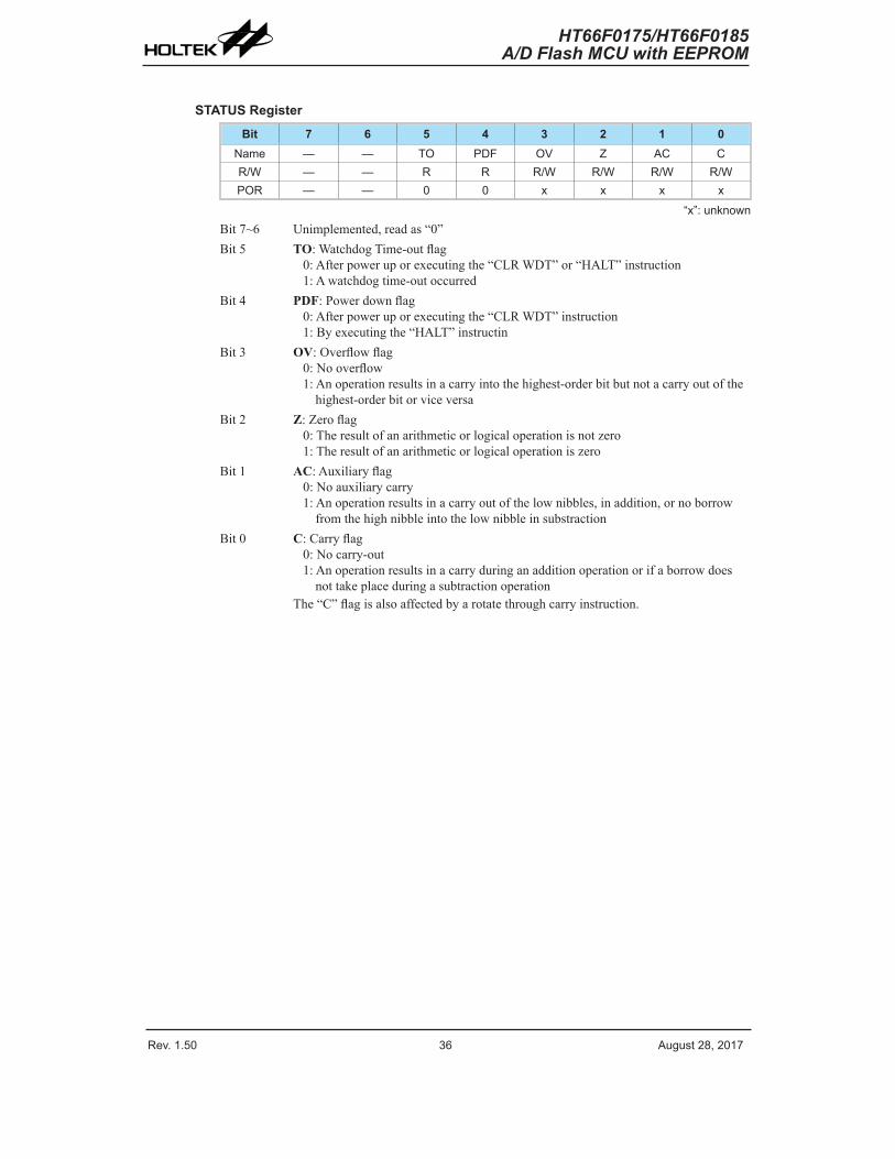
Rev. 1.50 36 ����st ��� �01� Rev. 1.50 3� ����st ��� �01�
HT66F0175/HT66F0185A/D Flash MCU with EEPROM
HT66F0175/HT66F0185A/D Flash MCU with EEPROM
STATUS Register
Bit 7 6 5 4 3 2 1 0Name — — TO PDF OV Z �C CR/W — — R R R/W R/W R/W R/WPOR — — 0 0 x x x x
“x”: �nknownBit7~6 Unimplemented,readas“0”Bit5 TO:WatchdogTime-outflag
0:Afterpoweruporexecutingthe“CLRWDT”or“HALT”instruction1:Awatchdogtime-outoccurred
Bit4 PDF:Powerdownflag0:Afterpoweruporexecutingthe“CLRWDT”instruction1:Byexecutingthe“HALT”instructin
Bit3 OV:Overflowflag0:Nooverflow1:Anoperationresultsinacarryintothehighest-orderbitbutnotacarryoutofthehighest-orderbitorviceversa
Bit2 Z:Zeroflag0:Theresultofanarithmeticorlogicaloperationisnotzero1:Theresultofanarithmeticorlogicaloperationiszero
Bit1 AC:Auxiliaryflag0:Noauxiliarycarry1:Anoperationresultsinacarryoutofthelownibbles,inaddition,ornoborrowfromthehighnibbleintothelownibbleinsubstraction
Bit0 C:Carryflag0:Nocarry-out1:Anoperationresultsinacarryduringanadditionoperationorifaborrowdoesnottakeplaceduringasubtractionoperation
The“C”flagisalsoaffectedbyarotatethroughcarryinstruction.

Rev. 1.50 36 ����st ��� �01� Rev. 1.50 3� ����st ��� �01�
HT66F0175/HT66F0185A/D Flash MCU with EEPROM
HT66F0175/HT66F0185A/D Flash MCU with EEPROM
EEPROM Data MemoryThesedevicescontainanareaof internalEEPROMDataMemory.EEPROM,whichstandsforElectricallyErasableProgrammableReadOnlyMemory, isby itsnatureanon-volatile formof re-programmablememory,withdata retentionevenwhen itspowersupply is removed.Byincorporating thiskindofdatamemory,awholenewhostofapplicationpossibilitiesaremadeavailabletothedesigner.TheavailabilityofEEPROMstorageallowsinformationsuchasproductidentificationnumbers,calibrationvalues,specificuserdata,systemsetupdataorotherproductinformationtobestoreddirectlywithin theproductmicrocontroller.TheprocessofreadingandwritingdatatotheEEPROMmemoryhasbeenreducedtoaverytrivialaffair.
EEPROM Data Memory StructureTheEEPROMDataMemorycapacity isup to128×8bits for theseriesofdevices.Unlike theProgramMemoryandRAMDataMemory, theEEPROMDataMemory isnotdirectlymappedintomemoryspaceandisthereforenotdirectlyaddressableinthesamewayastheothertypesofmemory.ReadandWriteoperationstotheEEPROMarecarriedoutinsinglebyteoperationsusinganaddressanddataregisterinbank0andasinglecontrolregisterinbank1.
Device Capacity AddressHT66F01�5 64 × � 00H ~ 3FHHT66F01�5 1�� × � 00H ~ �FH
EEPROM RegistersThreeregisterscontroltheoveralloperationoftheinternalEEPROMDataMemory.Thesearetheaddressregister,EEA,thedataregister,EEDandasinglecontrolregister,EEC.AsboththeEEAandEEDregistersarelocatedinbank0,theycanbedirectlyaccessedinthesamewasasanyotherSpecialFunctionRegister.TheEECregister,however,beinglocatedinbank1,canbereadfromorwritten to indirectlyusing theMP1MemoryPointerandIndirectAddressingRegister, IAR1.BecausetheEECcontrolregister is locatedataddress40Hinbank1, theMP1MemoryPointerregistermustfirstbesettothevalue40HandtheBankPointerregister,BP,settothevalue,01H,beforeanyoperationsontheEECregisterareexecuted.
Register NameBit
7 6 5 4 3 2 1 0EE� (HT66F01�5) — — EE�5 EE�4 EE�3 EE�� EE�1 EE�0EE� (HT66F01�5) — EE�6 EE�5 EE�4 EE�3 EE�� EE�1 EE�0EED D� D6 D5 D4 D3 D� D1 D0EEC — — — — WREN WR RDEN RD
EEPROM Registers List
EEA Register – HT66F0175
Bit 7 6 5 4 3 2 1 0Name — — EE�5 EE�4 EE�3 EE�� EE�1 EE�0R/W — — R/W R/W R/W R/W R/W R/WPOR — — 0 0 0 0 0 0
Bit7~6 Unimplemented,readas“0”Bit5~0 EEA5~EEA0:DataEEPROMaddressbit5~bit0

Rev. 1.50 3� ����st ��� �01� Rev. 1.50 39 ����st ��� �01�
HT66F0175/HT66F0185A/D Flash MCU with EEPROM
HT66F0175/HT66F0185A/D Flash MCU with EEPROM
EEA Register – HT66F0185
Bit 7 6 5 4 3 2 1 0Name — EE�6 EE�5 EE�4 EE�3 EE�� EE�1 EE�0R/W — R/W R/W R/W R/W R/W R/W R/WPOR — 0 0 0 0 0 0 0
Bit7 Unimplemented,readas“0”Bit6~0 EEA6~EEA0:DataEEPROMaddressbit6~bit0
EED Register
Bit 7 6 5 4 3 2 1 0Name D� D6 D5 D4 D3 D� D1 D0R/W R/W R/W R/W R/W R/W R/W R/W R/WPOR 0 0 0 0 0 0 0 0
Bit7~0 D7~D0:DataEEPROMdatabit7~bit0
EEC Register
Bit 7 6 5 4 3 2 1 0Name — — — — WREN WR RDEN RDR/W — — — — R/W R/W R/W R/WPOR — — — — 0 0 0 0
Bit7~4 Unimplemented,readas“0”Bit3 WREN:DataEEPROMwriteenable
0:Disable1:Enable
This is theDataEEPROMWriteEnableBitwhichmustbesethighbeforeDataEEPROMwriteoperationsarecarriedout.Clearingthisbit tozerowill inhibitDataEEPROMwriteoperations.
Bit2 WR:EEPROMwritecontrol0:Writecyclehasfinished1:Activateawritecycle
This is theDataEEPROMWriteControlBitandwhensethighbytheapplicationprogramwillactivateawritecycle.Thisbitwillbeautomaticallyresettozerobythehardwareafterthewritecyclehasfinished.SettingthisbithighwillhavenoeffectiftheWRENhasnotfirstbeensethigh.
Bit1 RDEN:DataEEPROMreadenable0:Disable1:Enable
This is theDataEEPROMReadEnableBitwhichmustbesethighbeforeDataEEPROMreadoperationsarecarriedout.Clearingthisbit tozerowill inhibitDataEEPROMreadoperations.
Bit0 RD:EEPROMreadcontrol0:Readcyclehasfinished1:Activateareadcycle
This is theDataEEPROMReadControlBitandwhensethighbytheapplicationprogramwillactivateareadcycle.Thisbitwillbeautomaticallyresettozerobythehardwareafterthereadcyclehasfinished.SettingthisbithighwillhavenoeffectiftheRDENhasnotfirstbeensethigh.
Note:TheWREN,WR,RDENandRDcannotbesetto“1”atthesametimeinoneinstruction.TheWRandRDcannotbesetto“1”atthesametime.

Rev. 1.50 3� ����st ��� �01� Rev. 1.50 39 ����st ��� �01�
HT66F0175/HT66F0185A/D Flash MCU with EEPROM
HT66F0175/HT66F0185A/D Flash MCU with EEPROM
Reading Data from the EEPROMToreaddatafromtheEEPROM,thereadenablebit,RDEN,intheEECregistermustfirstbesethightoenablethereadfunction.TheEEPROMaddressofthedatatobereadmustthenbeplacedintheEEAregister.IftheRDbitintheEECregisterisnowsethigh,areadcyclewillbeinitiated.SettingtheRDbithighwillnotinitiateareadoperationif theRDENbithasnotbeenset.Whenthereadcycleterminates,theRDbitwillbeautomaticallyclearedtozero,afterwhichthedatacanbereadfromtheEEDregister.ThedatawillremainintheEEDregisteruntilanotherreadorwriteoperationisexecuted.Theapplicationprogramcanpoll theRDbit todeterminewhenthedataisvalidforreading.
Writing Data to the EEPROMTowritedatatotheEEPROM,theEEPROMaddressofthedatatobewrittenmustfirstbeplacedin theEEAregisterandthedataplacedin theEEDregister.Thenthewriteenablebit,WREN,in theEECregistermustfirstbesethightoenablethewritefunction.After this, theWRbit intheEECregistermustbe immediatelysethigh to initiateawritecycle.These twoinstructionsmustbeexecutedconsecutively.Theglobal interruptbitEMIshouldalsofirstbeclearedbeforeimplementinganywriteoperations,andthensetagainafterthewritecyclehasstarted.Notethatsetting theWRbithighwillnot initiateawritecycle if theWRENbithasnotbeenset.As theEEPROMwritecycle iscontrolledusingan internal timerwhoseoperation isasynchronous tomicrocontrollersystemclock,acertaintimewillelapsebeforethedatawillhavebeenwrittenintotheEEPROM.DetectingwhenthewritecyclehasfinishedcanbeimplementedeitherbypollingtheWRbitintheEECregisterorbyusingtheEEPROMinterrupt.Whenthewritecycleterminates,theWRbitwillbeautomaticallyclearedtozerobythemicrocontroller,informingtheuserthatthedatahasbeenwrittentotheEEPROM.Theapplicationprogramcanthereforepoll theWRbit todeterminewhenthewritecyclehasended.
Write ProtectionProtectionagainst inadvertentwriteoperation isprovided inseveralways.After thedevice ispoweredon, theWriteEnablebit in thecontrol registerwillbeclearedpreventinganywriteoperations.Alsoatpower-ontheBankPointerregister,BP,willberesettozero,whichmeansthatDataMemorybank0willbeselected.AstheEEPROMcontrolregisteris locatedinbank1,thisaddsafurthermeasureofprotectionagainstspuriouswriteoperations.Duringnormalprogramoperation,ensuringthattheWriteEnablebitinthecontrolregisterisclearedwillsafeguardagainstincorrectwriteoperations.
EEPROM InterruptTheEEPROMwriteinterruptisgeneratedwhenanEEPROMwritecyclehasended.TheEEPROMinterruptmustfirstbeenabledbysettingtheDEEbitintherelevantinterruptregister.However,astheEEPROMiscontainedwithinaMulti-functionInterrupt,theassociatedmulti-functioninterruptenablebitmustalsobeset.WhenanEEPROMwritecycleends, theDEFrequest flagand itsassociatedmulti-functioninterruptrequestflagwillbothbeset.Iftheglobal,EEPROMandMulti-function interruptsareenabledandthestackisnotfull,a jumpto theassociatedMulti-functionInterruptvectorwilltakeplace.WhentheinterruptisservicedonlytheMulti-functioninterruptflagwillbeautomaticallyreset, theEEPROMinterruptflagmustbemanuallyresetbytheapplicationprogram.
Rev. 1.50 40 ����st ��� �01� Rev. 1.50 41 ����st ��� �01�
HT66F0175/HT66F0185A/D Flash MCU with EEPROM
HT66F0175/HT66F0185A/D Flash MCU with EEPROM
Programming ConsiderationsCaremustbetakenthatdataisnotinadvertentlywrittentotheEEPROM.ProtectioncanbePeriodicbyensuringthattheWriteEnablebitisnormallyclearedtozerowhennotwriting.AlsotheBankPointerregistercouldbenormallyclearedtozeroasthiswouldinhibitaccesstobank1wheretheEEPROMcontrol registerexist.Althoughcertainlynotnecessary,considerationmightbegivenintheapplicationprogramtothecheckingofthevalidityofnewwritedatabyasimplereadbackprocess.WhenwritingdatatheWRbitmustbesethighimmediatelyaftertheWRENbithasbeensethigh,toensurethewritecycleexecutescorrectly.TheglobalinterruptbitEMIshouldalsobeclearedbeforeawritecycleisexecutedandthenre-enabledafterthewritecyclestarts.NotethatthedeviceshouldnotentertheIDLEorSLEEPmodeuntiltheEEPROMreadorwriteoperationistotallycomplete.Otherwise,theEEPROMreadorwriteoperationwillfail.
Programming Example
Reading data from the EEPROM − polling methodMOV A, EEPROM_ADRES ; user defined addressMOV EEA, AMOV A, 040H ; setup memory pointer MP1MOV MP1, A ; MP1 points to EEC registerMOV A, 01H ; setup Bank Pointer BPMOV BP, ASET IAR1.1 ; set RDEN bit, enable read operationsSET IAR1.0 ; start Read Cycle - set RD bitBACK:SZ IAR1.0 ; check for read cycle endJMP BACKCLR IAR1 ; disable EEPROM writeCLR BPMOV A, EED ; move read data to registerMOV READ_DATA, A
Writing Data to the EEPROM − polling methodMOV A, EEPROM_ADRES ; user defined addressMOV EEA, AMOV A, EEPROM_DATA ; user defined dataMOV EED, AMOV A, 040H ; setup memory pointer MP1MOV MP1, A ; MP1 points to EEC registerMOV A, 01H ; setup Bank Pointer BPMOV BP, ACLR EMISET IAR1.3 ; set WREN bit, enable write operationsSET IAR1.2 ; start Write Cycle - set WR bitSET EMIBACK:SZ IAR1.2 ; check for write cycle endJMP BACKCLR IAR1 ; disable EEPROM writeCLR BP
Rev. 1.50 40 ����st ��� �01� Rev. 1.50 41 ����st ��� �01�
HT66F0175/HT66F0185A/D Flash MCU with EEPROM
HT66F0175/HT66F0185A/D Flash MCU with EEPROM
OscillatorVariousoscillatortypesoffertheuserawiderangeoffunctionsaccordingtotheirvariousapplicationrequirements.Theflexiblefeaturesoftheoscillatorfunctionsensurethatthebestoptimisationcanbeachievedintermsofspeedandpowersaving.Oscillatorselectionsandoperationareselectedthroughacombinationofconfigurationoptionsandrelevantcontrolregisters.
Oscillator OverviewInadditiontobeingthesourceofthemainsystemclocktheoscillatorsalsoprovideclocksourcesfor theWatchdogTimerandTimeBaseInterrupts.Externaloscillators requiringsomeexternalcomponentsaswellasfullyintegratedinternaloscillators,requiringnoexternalcomponents,areprovidedtoformawiderangeofbothfastandslowsystemoscillators.Alloscillatoroptionsareselectedthroughconfigurationoptions.Thehigherfrequencyoscillatorsprovidehigherperformancebutcarrywithitthedisadvantageofhigherpowerrequirements,whiletheoppositeisofcoursetrueforthelowerfrequencyoscillators.Withthecapabilityofdynamicallyswitchingbetweenfastandslowsystemclock,thedevicehastheflexibilitytooptimizetheperformance/powerratio,afeatureespeciallyimportantinpowersensitiveportableapplications.
Type Name Frequency PinsHi�h Speed External Crystal HXT 400 kHz~�0 MHz OSC1/OSC�Hi�h Speed Internal RC HIRC �/1�/16 MHz —Low Speed External Crystal LXT 3�.�6� kHz XT1/XT�Low Speed Internal RC LIRC 3� kHz —
Oscillator Types
System Clock ConfigurationsTherearefourmethodsofgeneratingthesystemclock,twohighspeedoscillatorsforalldevicesandtwolowspeedoscillators.Thehighspeedoscillatoristheexternalcrystal/ceramicoscillator,HXT,andtheinternal8/12/16MHzRCoscillator,HIRC.Thetwolowspeedoscillatorsaretheinternal32kHzRCoscillator,LIRC,andtheexternal32.768kHzcrystaloscillator,LXT.SelectingwhethertheloworhighspeedoscillatorisusedasthesystemoscillatorisimplementedusingtheHLCLKbitandCKS2~CKS0bitsintheSMODregisterandasthesystemclockcanbedynamicallyselected.
The actual source clockused for eachof thehigh and low speedoscillators is chosenviaconfigurationoptions.The frequencyof the slowspeedorhigh speed systemclock is alsodeterminedusing theHLCLKbitandCKS2~CKS0bits in theSMODregister.Note that twooscillatorselectionsmustbemadenamelyonehighspeedandonelowspeedsystemoscillators.
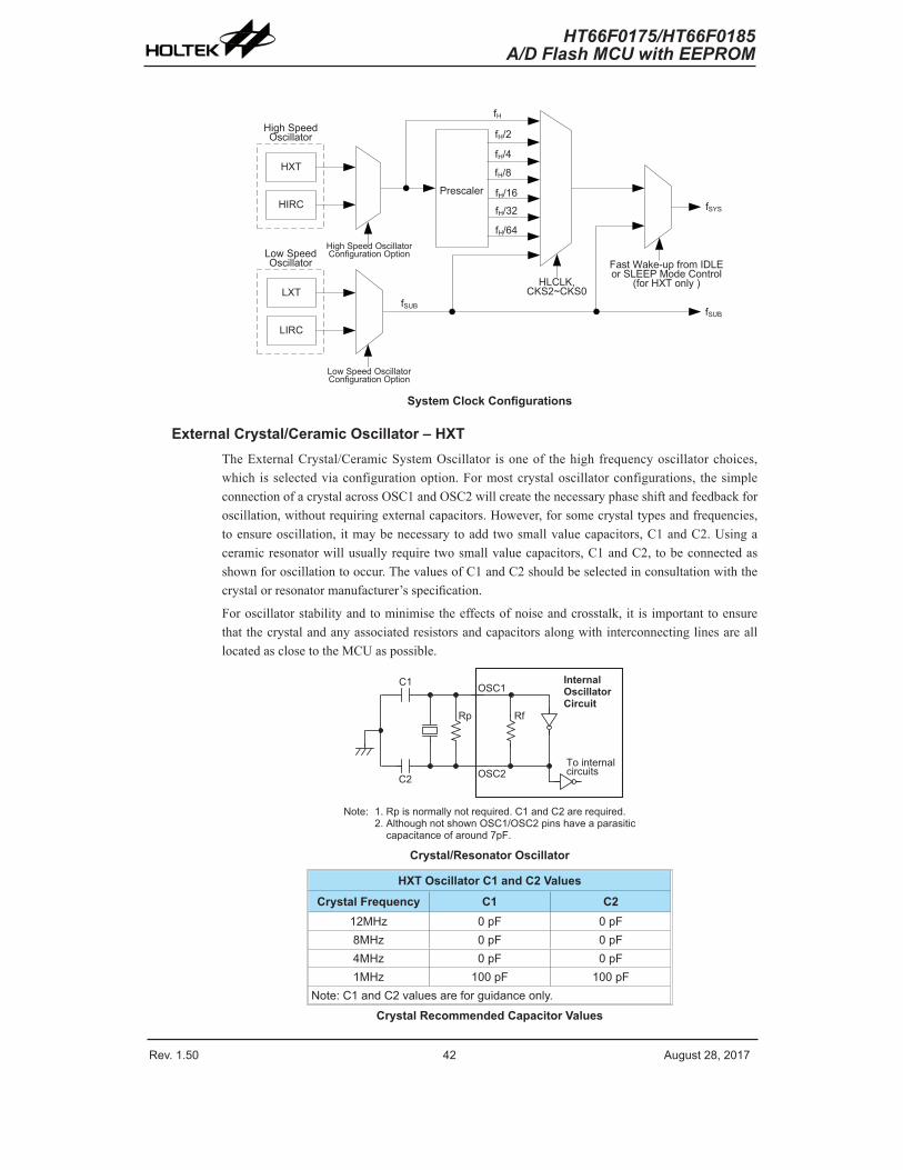
Rev. 1.50 4� ����st ��� �01� Rev. 1.50 43 ����st ��� �01�
HT66F0175/HT66F0185A/D Flash MCU with EEPROM
HT66F0175/HT66F0185A/D Flash MCU with EEPROM
HIRCPrescaler
fH
LXT
Hi�h Speed Oscillator
Low Speed Oscillator
fH/�
fH/16
fH/64
fH/�
fH/4
fH/3�
HLCLK�CKS�~CKS0
fSYS
fSUBfSUB
LIRC
HXT
fH
Hi�h Speed Oscillator Confi��ration Option
Low Speed Oscillator Confi��ration Option
Fast Wake-�p from IDLE or SLEEP Mode Control
(for HXT only )
System Clock Configurations
External Crystal/Ceramic Oscillator – HXTTheExternalCrystal/CeramicSystemOscillator isoneof thehighfrequencyoscillatorchoices,whichisselectedviaconfigurationoption.Formostcrystaloscillatorconfigurations, thesimpleconnectionofacrystalacrossOSC1andOSC2willcreatethenecessaryphaseshiftandfeedbackforoscillation,withoutrequiringexternalcapacitors.However,forsomecrystaltypesandfrequencies,toensureoscillation, itmaybenecessarytoaddtwosmallvaluecapacitors,C1andC2.Usingaceramicresonatorwillusuallyrequiretwosmallvaluecapacitors,C1andC2,tobeconnectedasshownforoscillationtooccur.ThevaluesofC1andC2shouldbeselectedinconsultationwiththecrystalorresonatormanufacturer’sspecification.
Foroscillatorstabilityandtominimisetheeffectsofnoiseandcrosstalk, it isimportanttoensurethatthecrystalandanyassociatedresistorsandcapacitorsalongwithinterconnectinglinesarealllocatedasclosetotheMCUaspossible.
� � � �
� � � �
� �
� � � � � � � � � � �� � � � � � �
� � � � � � � �� � � � � � � � � �� � � � � � �
� �
� �
� �
� � � � � � � � � � � � � � � � � � � � � � � � � � � � � � � � � � � � � � � � � � � � � � � � � � � � � � � �� � � � � � � � � � � � � � � � � � � � � � � � � � � � � � � � � � � � � � � � � � � � � � � � � � � �� � � � � � � � � � � � � � � � � � � � � � � � � � � � �
Crystal/Resonator Oscillator
HXT Oscillator C1 and C2 Values
Crystal Frequency C1 C21�MHz 0 pF 0 pF�MHz 0 pF 0 pF4MHz 0 pF 0 pF1MHz 100 pF 100 pF
Note: C1 and C� val�es are for ��idance only.
Crystal Recommended Capacitor Values
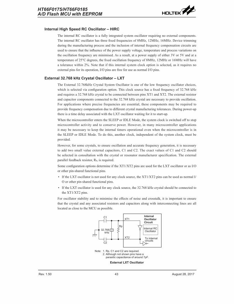
Rev. 1.50 4� ����st ��� �01� Rev. 1.50 43 ����st ��� �01�
HT66F0175/HT66F0185A/D Flash MCU with EEPROM
HT66F0175/HT66F0185A/D Flash MCU with EEPROM
Internal High Speed RC Oscillator – HIRCTheinternalRCoscillatorisafullyintegratedsystemoscillatorrequiringnoexternalcomponents.TheinternalRCoscillatorhasthreefixedfrequenciesof8MHz,12MHz,16MHz.Devicetrimmingduringthemanufacturingprocessandtheinclusionofinternalfrequencycompensationcircuitsareusedtoensurethattheinfluenceofthepowersupplyvoltage,temperatureandprocessvariationsontheoscillationfrequencyareminimised.Asaresult,atapowersupplyofeither3Vor5Vandatatemperatureof25°Cdegrees,thefixedoscillationfrequencyof8MHz,12MHzor16MHzwillhaveatolerancewithin2%.Notethat if this internalsystemclockoptionisselected,asitrequiresnoexternalpinsforitsoperation,I/OpinsarefreeforuseasnormalI/Opins.
External 32.768 kHz Crystal Oscillator – LXTTheExternal32.768kHzCrystalSystemOscillatorisoneofthelowfrequencyoscillatorchoices,whichisselectedviaconfigurationoption.Thisclocksourcehasafixedfrequencyof32.768kHzandrequiresa32.768kHzcrystaltobeconnectedbetweenpinsXT1andXT2.Theexternalresistorandcapacitorcomponentsconnectedtothe32.768kHzcrystalarenecessarytoprovideoscillation.Forapplicationswhereprecise frequenciesareessential, thesecomponentsmayberequired toprovidefrequencycompensationduetodifferentcrystalmanufacturingtolerances.Duringpower-upthereisatimedelayassociatedwiththeLXToscillatorwaitingforittostart-up.
WhenthemicrocontrollerenterstheSLEEPorIDLEMode,thesystemclockisswitchedofftostopmicrocontrolleractivityand toconservepower.However, inmanymicrocontrollerapplicationsitmaybenecessary tokeep the internal timersoperationalevenwhenthemicrocontroller is intheSLEEPorIDLEMode.Todothis,anotherclock, independentof thesystemclock,mustbeprovided.
However,forsomecrystals,toensureoscillationandaccuratefrequencygeneration,itisnecessarytoadd twosmallvalueexternalcapacitors,C1andC2.TheexactvaluesofC1andC2shouldbeselectedinconsultationwiththecrystalorresonatormanufacturerspecification.Theexternalparallelfeedbackresistor,RP,isrequired.
SomeconfigurationoptionsdetermineiftheXT1/XT2pinsareusedfortheLXToscillatororasI/Oorotherpin-sharedfunctionalpins.
• IftheLXToscillatorisnotusedforanyclocksource,theXT1/XT2pinscanbeusedasnormalI/Oorotherpin-sharedfunctionalpins.
• IftheLXToscillatorisusedforanyclocksource,the32.768kHzcrystalshouldbeconnectedtotheXT1/XT2pins.
Foroscillatorstabilityandtominimisetheeffectsofnoiseandcrosstalk, it isimportanttoensurethatthecrystalandanyassociatedresistorsandcapacitorsalongwithinterconnectinglinesarealllocatedasclosetotheMCUaspossible.
� � � � � � � � � � �� � � � � � � �
� � � � � � � �� � � � � � � � � �� � � � � � �
� �
� �
� �
� � � � � � � � � � � � � � � � � � � � � � � � � � � � � � �� � � � � � � � � � � � � � � � � � � � � � � � � � � � � � � � �� � � � � � � � � � � � � � � � � � � � � � � � � � � � � � � � � � � � � � �
� � � � � � � � � � �� � � � � � � � � �� � � � � �
�
� � �
� � �
External LXT Oscillator

Rev. 1.50 44 ����st ��� �01� Rev. 1.50 45 ����st ��� �01�
HT66F0175/HT66F0185A/D Flash MCU with EEPROM
HT66F0175/HT66F0185A/D Flash MCU with EEPROM
LXT Oscillator C1 and C2 Values
Crystal Frequency C1 C23�.�6�kHz 10pF 10pF
Note: 1. C1 and C� val�es are for ��idance only.�. RP=5MΩ~10MΩ is recommended.
32.768kHz Crystal Recommended Capacitor Values
LXT Oscillator Low Power FunctionTheLXToscillatorcanfunctioninoneoftwomodes,theQuickStartModeandtheLowPowerMode.ThemodeselectionisexecutedusingtheLXTLPbitintheTBCregister.
LXTLP LXT Operating Mode0 Q�ick Start1 Low-Power
Afterpoweron,theLXTLPbitwillbeautomaticallyclearedtozeroensuringthattheLXToscillatoris in theQuickStartoperatingmode.IntheQuickStartModetheLXToscillatorwillpowerupandstabilisequickly.However,after theLXToscillatorhas fullypoweredup itcanbeplacedintotheLow-powermodebysettingtheLXTLPbithigh.Theoscillatorwillcontinuetorunbutwithreducedcurrentconsumption,asthehighercurrentconsumptionisonlyrequiredduringtheLXToscillatorstart-up.Inpowersensitiveapplications,suchasbatteryapplications,wherepowerconsumptionmustbekepttoaminimum,itisthereforerecommendedthattheapplicationprogramsets theLXTLPbithighabout2secondsafterpower-on.Itshouldbenotedthat,nomatterwhatconditiontheLXTLPbit isset to, theLXToscillatorwillalwaysfunctionnormallyandtheonlydifferenceisthatitwilltakemoretimetostartupifintheLow-powermode.
Internal 32kHz Oscillator – LIRCTheInternal32kHzSystemOscillator isoneof the lowfrequencyoscillatorchoices,which isselectedviaconfigurationoption.It isafullyintegratedRCoscillatorwithatypicalfrequencyof32kHzat5V,requiringnoexternalcomponentsfor its implementation.Device trimmingduringthemanufacturingprocessandtheinclusionofinternalfrequencycompensationcircuitsareusedtoensurethattheinfluenceofthepowersupplyvoltage,temperatureandprocessvariationsontheoscillationfrequencyareminimised.Asaresult,atapowersupplyof5Vandatatemperatureof25°Cdegrees,thefixedoscillationfrequencyof32kHzwillhaveatolerancewithin10%.
Supplementary OscillatorsThelowspeedoscillators,inadditiontoprovidingasystemclocksourcearealsousedtoprovideaclocksource to twootherdevicefunctions.Theseare theWatchdogTimerandtheTimeBaseInterrupts.

Rev. 1.50 44 ����st ��� �01� Rev. 1.50 45 ����st ��� �01�
HT66F0175/HT66F0185A/D Flash MCU with EEPROM
HT66F0175/HT66F0185A/D Flash MCU with EEPROM
Operating Modes and System ClocksPresentdayapplicationsrequirethat theirmicrocontrollershavehighperformancebutoftenstilldemandthattheyconsumeaslittlepoweraspossible,conflictingrequirementsthatareespeciallytrueinbatterypoweredportableapplications.Thefastclocksrequiredforhighperformancewillbytheirnatureincreasecurrentconsumptionandofcoursevice-versa, lowerspeedclocksreducecurrentconsumption.AsHoltekhasprovidedthesedeviceswithbothhighandlowspeedclocksourcesandthemeanstoswitchbetweenthemdynamically,theusercanoptimisetheoperationoftheirmicrocontrollertoachievethebestperformance/powerratio.
System ClocksThedeviceshavemanydifferentclocksourcesforboththeCPUandperipheralfunctionoperation.Byprovidingtheuserwithawiderangeofclockoptionsusingconfigurationoptionsandregisterprogramming,aclocksystemcanbeconfiguredtoobtainmaximumapplicationperformance.
Themainsystemclock,cancomefromeitherahighfrequencyfHorlowfrequencyfSUBsource,andisselectedusingtheHLCLKbitandCKS2~CKS0bitsintheSMODregister.ThehighspeedsystemclockcanbesourcedfromeitheranHXTorHIRCoscillator,selectedviaaconfigurationoption.ThelowspeedsystemclocksourcecanbesourcedfrominternalclockfSUB.IffSUBisselectedthenitcanbesourcedbyeithertheLXTorLIRCoscillator,selectedviaaconfigurationoption.Theotherchoice,whichisadividedversionofthehighspeedsystemoscillatorhasarangeoffH/2~fH/64.
Therearetwoadditionalinternalclocksfor theperipheralcircuits, thesubstituteclock,fSUB,andtheTimeBaseclock, fTBC.Eachof these internalclocks issourcedbyeither theLXTorLIRCoscillators,selectedviaconfigurationoptions.ThefSUBclockisusedtoprovideasubstituteclockforthemicrocontrollerjustafterawake-uphasoccurredtoenablefasterwake-uptimes.
HIRCPrescaler
fH
LXT
Hi�h Speed Oscillator
Low Speed Oscillator
fH/�
fH/16
fH/64
fH/�
fH/4
fH/3�
HLCLK�CKS�~CKS0
fSYS
fSUBfSUB
LIRC
HXT
fH
Hi�h Speed Oscillator Confi��ration Option
Low Speed Oscillator Confi��ration Option
Fast Wake-�p from IDLE or SLEEP Mode Control
(for HXT only )
fSUB
IDLENfTBC
fSYS/4
TBCK
fTB Time Base
WDTfSUB
fTBC
Device Clock ConfigurationsNote:WhenthesystemclocksourcefSYSisswitchedtofSUBfromfH,thehighspeedoscillatorwill
stoptoconservethepower.ThusthereisnofH~fH/64forperipheralcircuittouse.
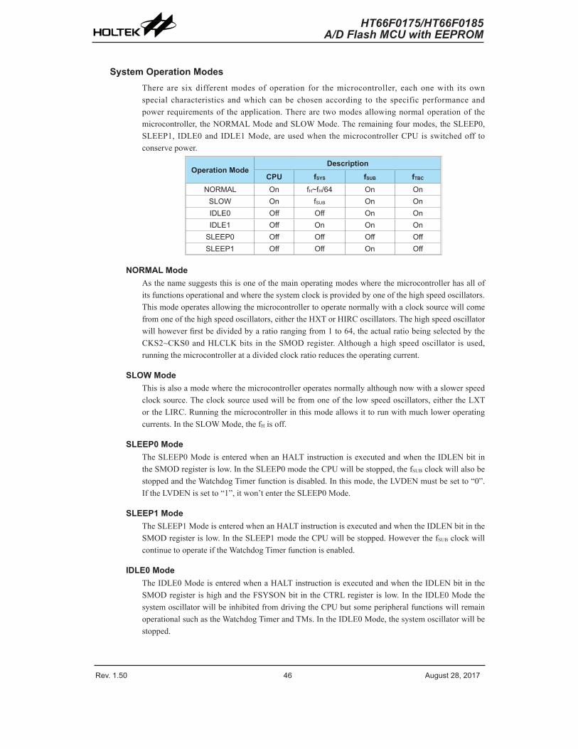
Rev. 1.50 46 ����st ��� �01� Rev. 1.50 4� ����st ��� �01�
HT66F0175/HT66F0185A/D Flash MCU with EEPROM
HT66F0175/HT66F0185A/D Flash MCU with EEPROM
System Operation ModesThere are six differentmodesof operation for themicrocontroller, eachonewith its ownspecial characteristics andwhichcanbe chosenaccording to the specificperformanceandpowerrequirementsof theapplication.Thereare twomodesallowingnormaloperationof themicrocontroller, theNORMALModeandSLOWMode.Theremainingfourmodes,theSLEEP0,SLEEP1, IDLE0andIDLE1Mode,areusedwhen themicrocontrollerCPUisswitchedoff toconservepower.
Operation ModeDescription
CPU fSYS fSUB fTBC
NORM�L On fH~fH/64 On OnSLOW On fSUB On OnIDLE0 Off Off On OnIDLE1 Off On On On
SLEEP0 Off Off Off OffSLEEP1 Off Off On Off
NORMAL ModeAsthenamesuggeststhisisoneofthemainoperatingmodeswherethemicrocontrollerhasallofitsfunctionsoperationalandwherethesystemclockisprovidedbyoneofthehighspeedoscillators.Thismodeoperatesallowingthemicrocontrollertooperatenormallywithaclocksourcewillcomefromoneofthehighspeedoscillators,eithertheHXTorHIRCoscillators.Thehighspeedoscillatorwillhoweverfirstbedividedbyaratiorangingfrom1to64,theactualratiobeingselectedbytheCKS2~CKS0andHLCLKbits in theSMODregister.Althoughahighspeedoscillator isused,runningthemicrocontrolleratadividedclockratioreducestheoperatingcurrent.
SLOW ModeThisisalsoamodewherethemicrocontrolleroperatesnormallyalthoughnowwithaslowerspeedclocksource.Theclocksourceusedwillbefromoneofthelowspeedoscillators,eithertheLXTortheLIRC.Runningthemicrocontrollerinthismodeallowsittorunwithmuchloweroperatingcurrents.IntheSLOWMode,thefHisoff.
SLEEP0 ModeTheSLEEP0ModeisenteredwhenanHALTinstructionisexecutedandwhentheIDLENbitintheSMODregisterislow.IntheSLEEP0modetheCPUwillbestopped,thefSUBclockwillalsobestoppedandtheWatchdogTimerfunctionisdisabled.Inthismode,theLVDENmustbesetto“0”.IftheLVDENissetto“1”,itwon’tentertheSLEEP0Mode.
SLEEP1 ModeTheSLEEP1ModeisenteredwhenanHALTinstructionisexecutedandwhentheIDLENbitintheSMODregisterislow.IntheSLEEP1modetheCPUwillbestopped.HoweverthefSUBclockwillcontinuetooperateiftheWatchdogTimerfunctionisenabled.
IDLE0 ModeTheIDLE0ModeisenteredwhenaHALTinstructionisexecutedandwhentheIDLENbitintheSMODregisterishighandtheFSYSONbitintheCTRLregisterislow.IntheIDLE0ModethesystemoscillatorwillbeinhibitedfromdrivingtheCPUbutsomeperipheralfunctionswillremainoperationalsuchastheWatchdogTimerandTMs.IntheIDLE0Mode,thesystemoscillatorwillbestopped.
Rev. 1.50 46 ����st ��� �01� Rev. 1.50 4� ����st ��� �01�
HT66F0175/HT66F0185A/D Flash MCU with EEPROM
HT66F0175/HT66F0185A/D Flash MCU with EEPROM
IDLE1 ModeTheIDLE1ModeisenteredwhenanHALTinstructionisexecutedandwhentheIDLENbitintheSMODregisterishighandtheFSYSONbitintheCTRLregisterishigh.IntheIDLE1ModethesystemoscillatorwillbeinhibitedfromdrivingtheCPUbutmaycontinuetoprovideaclocksourcetokeepsomeperipheralfunctionsoperationalsuchastheWatchdogTimerandTMs.IntheIDLE1Mode,thesystemoscillatorwillcontinuetorun,andthissystemoscillatormaybehighspeedorlowspeedsystemoscillator.
Control RegistersAsingleregister,SMOD,isusedforoverallcontroloftheinternalclockswithinthedevices.
SMOD Register
Bit 7 6 5 4 3 2 1 0Name CKS� CKS1 CKS0 FSTEN LTO HTO IDLEN HLCLKR/W R/W R/W R/W R/W R R R/W R/WPOR 0 0 0 0 0 0 1 1
Bit7~5 CKS2~CKS0:SystemclockselectionwhenHLCLKis“0”000:fSUB
001:fSUB
010:fH/64011:fH/32100:fH/16101:fH/8110:fH/4111:fH/2
Thesethreebitsareusedtoselectwhichclockisusedasthesystemclocksource.Inadditiontothesystemclocksource,whichcanbeeithertheLXTorLIRC,adividedversionof thehighspeedsystemoscillatorcanalsobechosenas thesystemclocksource.
Bit4 FSTEN:FastWake-upControl(onlyforHXT)0:Disable1:Enable
This is theFastWake-upControlbitwhichdetermines if the fSUBclocksource isinitiallyusedafterthedevicewakesup.Whenthebitishigh,thefSUBclocksourcecanbeusedasatemporarysystemclocktoprovideafasterwakeuptimeasthefSUBclockisavailable.
Bit3 LTO:Lowspeedsystemoscillatorreadyflag0:Notready1:Ready
Thisisthelowspeedsystemoscillatorreadyflagwhichindicateswhenthelowspeedsystemoscillator isstableafterpoweronresetorawake-uphasoccurred.TheflagwillbelowwhenintheSLEEP0Modebutafterawake-uphasoccurred,theflagwillchangetoahighlevelafter128clockcycles if theLXToscillator isusedand1~2clockcyclesiftheLIRCoscillatorisused.

Rev. 1.50 4� ����st ��� �01� Rev. 1.50 49 ����st ��� �01�
HT66F0175/HT66F0185A/D Flash MCU with EEPROM
HT66F0175/HT66F0185A/D Flash MCU with EEPROM
Bit2 HTO:Highspeedsystemoscillatorreadyflag0:Notready1:Ready
This is thehighspeedsystemoscillator readyflagwhich indicateswhen thehighspeedsystemoscillator isstable.Thisflag isclearedto“0”byhardwarewhenthedevicesarepoweredonandthenchangestoahighlevelafterthehighspeedsystemoscillatorisstable.Thereforethisflagwillalwaysbereadas“1”bytheapplicationprogramafterdevicepower-on.TheflagwillbelowwhenintheSLEEPorIDLE0Modebutafterawake-uphasoccurred,theflagwillchangetoahighlevelafter512clockcyclesiftheHXToscillatorisusedandafter15~16clockcyclesiftheHIRCoscillatorisused.
Bit1 IDLEN:IDLEmodecontrol0:Disable1:Enable
This is the IDLEmodecontrolbitanddetermineswhathappenswhen theHALTinstructionisexecuted.If thisbit ishigh,whenaHALTinstructionisexecured,thedevicewillentertheIDLEmode.IntheIDLEmodetheCPUwillstoprunningbutthesystemclockwillcontinye tokeep theperipheral functionsoperational, if theFSYSONbitishigh.IftheFSYSONbitislow,theCPUandthesystemclockwillallstopinIDLE0mode.Ifthebitislow,thedeviceswillentertheSLEEPmodewhenaHALTinstructionisexecuted.
Bit0 HLCLK:Systemclockselection0:fH/2~fH/64orfSUB
1:fHThisbit isused toselect if the fHclockor the fH/2~fH/64or fSUBclock isusedasthesystemclock.Whenthebit ishigh thefHclockwillbeselectedandif lowthefH/2~fH/64or fSUBclockwillbeselected.WhensystemclockswitchesfromthefHclocktothefSUBclockandthefHclockwillbeautomaticallyswitchedofftoconservepower.
CTRL Register
Bit 7 6 5 4 3 2 1 0Name FSYSON — — — — LVRF LRF WRFR/W R/W — — — — R/W R/W R/WPOR 0 — — — — x 0 0
“x”: �nknownBit7 FSYSON:fSYSControlinIDLEMode
0:Disable1:Enable
ThisbitisusedtocontrolwhetherthesystemclockisswitchedonornotintheIDLEMode.Ifthisbitissetto“0”,thesystemclockwillbeswitchedoffintheIDLEMode.However,thesystemclockwillbeswitchedonintheIDLEModewhentheFSYSONbitissetto“1”.
Bit6~3 Unimplemented,readas“0”Bit2 LVRF:LVRfunctionresetflag
Describedelsewhere.Bit1 LRF:LVRcontrolregistersoftwareresetflag
Describedelsewhere.Bit0 WRF:WDTcontrolregistersoftwareresetflag
Describedelsewhere.
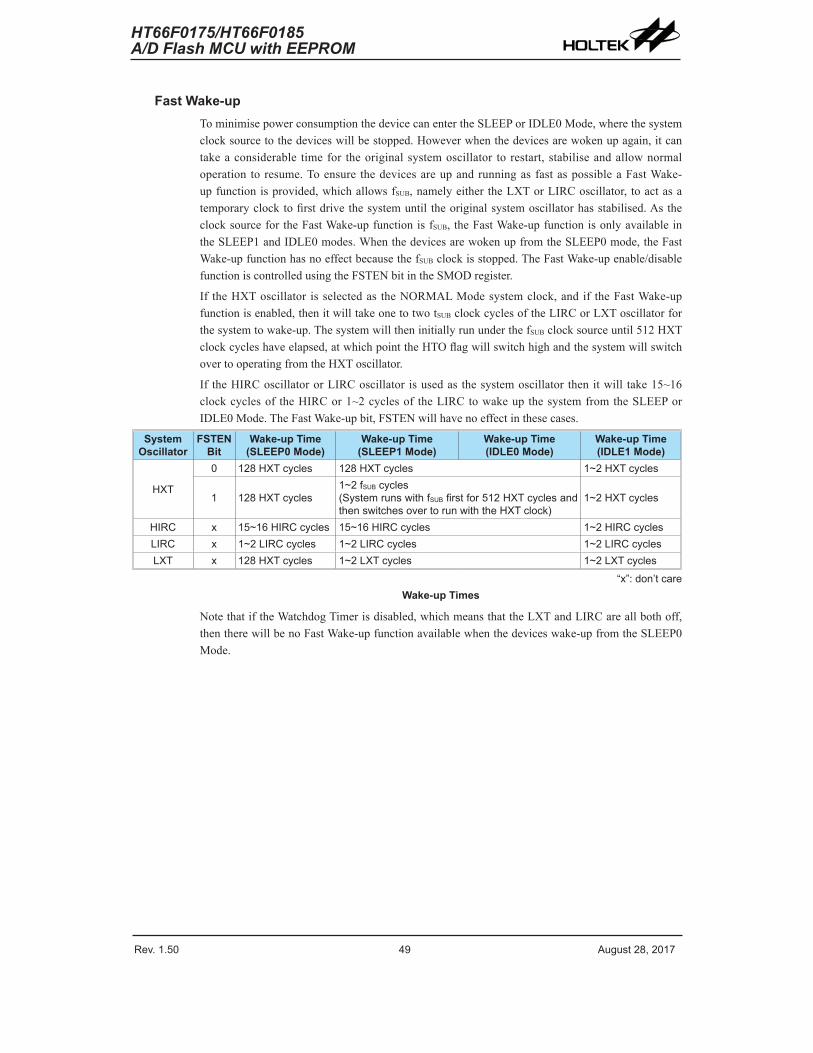
Rev. 1.50 4� ����st ��� �01� Rev. 1.50 49 ����st ��� �01�
HT66F0175/HT66F0185A/D Flash MCU with EEPROM
HT66F0175/HT66F0185A/D Flash MCU with EEPROM
Fast Wake-upTominimisepowerconsumptionthedevicecanentertheSLEEPorIDLE0Mode,wherethesystemclocksourcetothedeviceswillbestopped.Howeverwhenthedevicesarewokenupagain,itcantakeaconsiderable timefor theoriginalsystemoscillator torestart, stabiliseandallownormaloperation toresume.Toensure thedevicesareupandrunningasfastaspossibleaFastWake-upfunctionisprovided,whichallowsfSUB,namelyeithertheLXTorLIRCoscillator, toactasatemporaryclocktofirstdrivethesystemuntil theoriginalsystemoscillatorhasstabilised.AstheclocksourcefortheFastWake-upfunctionisfSUB, theFastWake-upfunctionisonlyavailableintheSLEEP1andIDLE0modes.WhenthedevicesarewokenupfromtheSLEEP0mode,theFastWake-upfunctionhasnoeffectbecausethefSUBclockisstopped.TheFastWake-upenable/disablefunctioniscontrolledusingtheFSTENbitintheSMODregister.
If theHXToscillator isselectedas theNORMALModesystemclock,andif theFastWake-upfunctionisenabled,thenitwilltakeonetotwotSUBclockcyclesoftheLIRCorLXToscillatorforthesystemtowake-up.ThesystemwilltheninitiallyrununderthefSUBclocksourceuntil512HXTclockcycleshaveelapsed,atwhichpointtheHTOflagwillswitchhighandthesystemwillswitchovertooperatingfromtheHXToscillator.
If theHIRCoscillatororLIRCoscillator isusedasthesystemoscillator thenitwill take15~16clockcyclesof theHIRCor1~2cyclesof theLIRCtowakeupthesystemfromtheSLEEPorIDLE0Mode.TheFastWake-upbit,FSTENwillhavenoeffectinthesecases.
System Oscillator
FSTEN Bit
Wake-up Time (SLEEP0 Mode)
Wake-up Time (SLEEP1 Mode)
Wake-up Time (IDLE0 Mode)
Wake-up Time (IDLE1 Mode)
HXT
0 1�� HXT cycles 1�� HXT cycles 1~� HXT cycles
1 1�� HXT cycles1~� fSUB cycles(System r�ns with fSUB first for 512 HXT cycles and then switches over to r�n with the HXT clock)
1~� HXT cycles
HIRC x 15~16 HIRC cycles 15~16 HIRC cycles 1~� HIRC cyclesLIRC x 1~� LIRC cycles 1~� LIRC cycles 1~� LIRC cyclesLXT x 1�� HXT cycles 1~� LXT cycles 1~� LXT cycles
“x”: don’t careWake-up Times
NotethatiftheWatchdogTimerisdisabled,whichmeansthattheLXTandLIRCareallbothoff,thentherewillbenoFastWake-upfunctionavailablewhenthedeviceswake-upfromtheSLEEP0Mode.

Rev. 1.50 50 ����st ��� �01� Rev. 1.50 51 ����st ��� �01�
HT66F0175/HT66F0185A/D Flash MCU with EEPROM
HT66F0175/HT66F0185A/D Flash MCU with EEPROM
Operating Mode SwitchingThesedevicescanswitchbetweenoperatingmodesdynamicallyallowingtheusertoselectthebestperformance/powerratiofor thepresent taskinhand.Inthiswaymicrocontrolleroperationsthatdonotrequirehighperformancecanbeexecutedusingslowerclocksthusrequiringlessoperatingcurrentandprolongingbatterylifeinportableapplications.
Insimple terms,ModeSwitchingbetween theNORMALModeandSLOWMode isexecutedusingtheHLCLKbitandCKS2~CKS0bitsintheSMODregisterwhileModeSwitchingfromtheNORMAL/SLOWModestotheSLEEP/IDLEModesisexecutedviatheHALTinstruction.WhenaHALTinstructionisexecuted,whetherthedevicesentertheIDLEModeortheSLEEPModeisdeterminedbytheconditionof theIDLENbit intheSMODregisterandtheFSYSONbit intheCTRLregister.
WhentheHLCLKbitswitchestoalowlevel,whichimpliesthatclocksourceisswitchedfromthehighspeedclock,fH, totheclocksource,fH/2~fH/64orfSUB.If theclockisfromthefSUB, thehighspeedclocksourcewillstoprunningtoconservepower.Whenthishappens,itmustbenotedthatthefH/16andfH/64internalclocksourceswillalsostoprunning,whichmayaffecttheoperationofotherinternalfunctionssuchastheTMs.Theaccompamyingchartshowswhathappenswhenthedevicesmovebetweenthevariousoperatingmodes.
NORMALfSYS=fH~fH/64
fH onCPU r�nfSYS onfSUB onfTBC on
SLOWfSYS=fSUBfSUB on
CPU r�nfSYS onfH off
fTBC on
IDLE0H�LT instr�ction exec�ted
CPU stopIDLEN=1
FSYSON=0fSYS offfSUB onfTBC on
IDLE1H�LT instr�ction exec�ted
CPU stopIDLEN=1
FSYSON=1fSYS onfSUB onfTBC on
SLEEP1H�LT instr�ction exec�ted
CPU stopIDLEN=0
fSYS offfSUB onfTBC offWDT on
SLEEP0H�LT instr�ction exec�ted
CPU stopIDLEN=0
fSYS offfSUB offfTBC off
WDT & LVD off

Rev. 1.50 50 ����st ��� �01� Rev. 1.50 51 ����st ��� �01�
HT66F0175/HT66F0185A/D Flash MCU with EEPROM
HT66F0175/HT66F0185A/D Flash MCU with EEPROM
NORMAL Mode to SLOW Mode SwitchingWhenrunningintheNORMALMode,whichusesthehighspeedsystemoscillator,andthereforeconsumesmorepower,thesystemclockcanswitchtorunintheSLOWModebysettheHLCLKbitto“0”andsettheCKS2~CKS0bitsto“000”or“001”intheSMODregister.Thiswillthenusethelowspeedsystemoscillatorwhichwillconsumelesspower.Usersmaydecidetodothisforcertainoperationswhichdonotrequirehighperformanceandcansubsequentlyreducepowerconsumption.
TheSLOWModeissourcedfromtheLXTorLIRCoscillatordeterminedbytheconfigurationoptionandthereforerequiresthisoscillatortobestablebeforefullmodeswitchingoccurs.ThisismonitoredusingtheLTObitintheSMODregister.
NORMAL Mode
SLOW Mode
CKS�~CKS0 = 00xB &HLCLK = 0
SLEEP0 Mode
IDLEN=0H�LT instr�ction is exec�ted
SLEEP1 Mode
IDLE0 Mode
IDLE1 Mode
WDT and LVD are all off
IDLEN=0H�LT instr�ction is exec�ted
WDT is on
IDLEN=1� FSYSON=0H�LT instr�ction is exec�ted
IDLEN=1� FSYSON=1H�LT instr�ction is exec�ted

Rev. 1.50 5� ����st ��� �01� Rev. 1.50 53 ����st ��� �01�
HT66F0175/HT66F0185A/D Flash MCU with EEPROM
HT66F0175/HT66F0185A/D Flash MCU with EEPROM
SLOW Mode to NORMAL Mode SwitchingInSLOWmodethesystemuseseither theLXTorLIRClowspeedsystemoscillator.ToswitchbacktotheNARMALMode,wherethehighspeedsystemoscillatorisused,theHLCLKbitshouldbesetto“1”orHLCLKbitis“0”,butCKS2~CKS0fieldissetto“010”,“011”,“100”,“101”,“110”or“111”.Asacertainamountoftimewillberequiredforhighspeedsystemoscillatorstabilizationdependsuponwhichhighspeedsystemoscillatortypeisused.
NORMAL Mode
SLOW Mode
CKS2~CKS0 ≠ 000B or 001B as HLCLK = 0 or HLCLK = 1
SLEEP0 Mode
IDLEN=0HALT instruction is executed
SLEEP1 Mode
IDLE0 Mode
IDLE1 Mode
WDT and LVD are all off
IDLEN=0HALT instruction is executed
WDT is on
IDLEN=1, FSYSON=0HALT instruction is executed
IDLEN=1, FSYSON=1HALT instruction is executed
Entering the SLEEP0 ModeThereisonlyonewayforthedevicestoentertheSLEEP0Modeandthatistoexecutethe“HALT”instructionintheapplicationprogramwiththeIDLENbitintheSMODregisterequalto“0”andtheWDTandLVDbothoff.Whenthisinstructionisexecutedundertheconditionsdescribedabove,thefollowingwilloccur:
• Thesystemclock,WDTclockandTimeBaseclockwillbestoppedandtheapplicationprogramwillstopatthe"HALT"instruction.
• TheDataMemorycontentsandregisterswillmaintaintheirpresentcondition.
• TheWDTwillbeclearedandstoppednomatter if theWDTclocksourceorginatesfromtheLXTorLIRCoscillator.
• TheI/Oportswillmaintaintheirpresentconditions.
• Inthestatusregister,thePowerDownflagPDFwillbeset,andWDTtimeoutflagTOwillbecleared.

Rev. 1.50 5� ����st ��� �01� Rev. 1.50 53 ����st ��� �01�
HT66F0175/HT66F0185A/D Flash MCU with EEPROM
HT66F0175/HT66F0185A/D Flash MCU with EEPROM
Entering the SLEEP1 ModeThereisonlyonewayforthedevicestoentertheSLEEP1Modeandthatistoexecutethe“HALT”instructionintheapplicationprogramwiththeIDLENbitintheSMODregisterequalto“0”andtheWDTon.Whenthisinstructionisexecutedundertheconditionsdescribedabove,thefollowingwilloccur:
• ThesystemclockandTimeBaseclockwillbestoppedandtheapplicationprogramwillstopatthe"HALT"instruction,but theWDTwillremainwiththeclocksourcecomingfromthefSUBclock.
• TheDataMemorycontentsandregisterswillmaintaintheirpresentcondition.
• TheWDTwillbeclearedandresumecountingiftheWDTfunctionisenabled.
• TheI/Oportswillmaintaintheirpresentconditions.
• Inthestatusregister,thePowerDownflagPDFwillbeset,andWDTtimeoutflagTOwillbecleared.
Entering the IDLE0 ModeThereisonlyonewayforthedevicestoentertheIDLE0Modeandthatistoexecutethe“HALT”instructionintheapplicationprogramwiththeIDLENbitintheSMODregisterequalto“1”andtheFSYSONbit in theCTRLregisterequal to“0”.Whenthis instruction isexecutedunder theconditionsdescribedabove,thefollowingwilloccur:
• The systemclockwill be stoppedand the applicationprogramwill stopat the “HALT”instruction,butthefTBCandfSUBclockswillbeon.
• TheDataMemorycontentsandregisterswillmaintaintheirpresentcondition.
• TheWDTwillbeclearedandresumecountingiftheWDTfunctionisenabled.
• TheI/Oportswillmaintaintheirpresentconditions.
• Inthestatusregister,thePowerDownflagPDFwillbeset,andWDTtimeoutflagTOwillbecleared.
Entering the IDLE1 ModeThereisonlyonewayforthedevicestoentertheIDLE1Modeandthatistoexecutethe“HALT”instructionintheapplicationprogramwiththeIDLENbitintheSMODregisterequalto“1”andtheFSYSONbit in theCTRLregisterequal to“1”.Whenthis instruction isexecutedunder theconditionsdescribedabove,thefollowingwilloccur:
• Thesystemclock,fTBCandfSUBclockswillbeonbut theapplicationprogramwillstopat the“HALT”instruction.
• TheDataMemorycontentsandregisterswillmaintaintheirpresentcondition.
• TheWDTwillbeclearedandresumecountingiftheWDTfunctionisenabled.
• TheI/Oportswillmaintaintheirpresentconditions.
• Inthestatusregister,thePowerDownflagPDFwillbeset,andWDTtimeoutflagTOwillbecleared.
Rev. 1.50 54 ����st ��� �01� Rev. 1.50 55 ����st ��� �01�
HT66F0175/HT66F0185A/D Flash MCU with EEPROM
HT66F0175/HT66F0185A/D Flash MCU with EEPROM
Standby Current ConsiderationsAsthemainreasonforenteringtheSLEEPorIDLEModeistokeepthecurrentconsumptionofthedevicetoaslowavalueaspossible,perhapsonlyintheorderofseveralmicro-ampsexceptintheIDLE1Mode,thereareotherconsiderationswhichmustalsobetakenintoaccountbythecircuitdesignerifthepowerconsumptionistobeminimised.SpecialattentionmustbemadetotheI/Opinsonthedevice.Allhigh-impedanceinputpinsmustbeconnectedtoeitherafixedhighorlowlevelasanyfloatinginputpinscouldcreateinternaloscillationsandresultinincreasedcurrentconsumption.Thisalsoappliestodeviceswhichhavedifferentpackagetypes,astheremaybeunbonbedpins.Thesemusteitherbesetupasoutputsorifsetupasinputsmusthavepull-highresistorsconnected.
Caremustalsobetakenwiththeloads,whichareconnectedtoI/Opins,whicharesetupasoutputs.Theseshouldbeplacedinaconditioninwhichminimumcurrent isdrawnorconnectedonlytoexternalcircuits thatdonotdrawcurrent,suchasotherCMOSinputs.Alsonote thatadditionalstandbycurrentwillalsoberequirediftheLIRCoscillatorhasenabled.
In theIDLE1Mode thesystemoscillator ison, if thesystemoscillator is fromthehighspeedoscillator,theadditionalstandbycurrentwillalsobeperhapsintheorderofseveralhundredmicro-amps.
Wake-upTominimisepowerconsumptionthedevicecanenter theSLEEPoranyIDLEMode,wheretheCPUwillbeswitchedoff.However,whenthedeviceiswokenupagain,itwilltakeaconsiderabletimefortheoriginalsystemoscillatortorestart,stabliseandallownormaloperationtoresume.
AfterthesystementerstheSLEEPorIDLEMode,itcanbewokenupfromoneofvarioussourceslistedasfollows:
• AnexternalfallingedgeonPortA
• Asysteminterrupt
• AWDToverflow
Whenthedevicesexecutethe“HALT”instruction,itwillenterthePowerdownmodeandthePDFflagwillbesetto1.ThePDFflagwillbeclearedto0ifthedevicesexperienceasystempower-uporexecutestheclearWatchdogTimerinstruction.IfthesystemiswokenupbyaWDToverflow,aWatchdogTimerresetwillbeinitiatedandtheTOflagwillbesetto1.TheTOflagissetifaWDTtime-outoccursandcausesawake-upthatonlyresetstheProgramCounterandStackPointer,otherflagsremainintheiroriginalstatus.
EachpinonPortAcanbesetupusingthePAWUregistertopermitanegativetransitiononthepintowakeupthesystem.WhenaPortApinwake-upoccurs,theprogramwillresumeexecutionattheinstructionfollowingthe“HALT”instruction.If thesystemiswokenupbyaninterrupt, thentwopossiblesituationsmayoccur.Thefirstiswheretherelatedinterruptisdisabledortheinterruptisenabledbutthestackisfull,inwhichcasetheprogramwillresumeexecutionattheinstructionfollowingthe“HALT”instruction.Inthissituation,theinterruptwhichwokeupthedeviceswillnotbeimmediatelyserviced,butwillratherbeservicedlaterwhentherelatedinterruptisfinallyenabledorwhenastacklevelbecomesfree.Theothersituationiswheretherelatedinterruptisenabledandthestackisnotfull,inwhichcasetheregularinterruptresponsetakesplace.Ifaninterruptrequestflag issethighbeforeentering theSLEEPorIDLEMode, thewake-upfunctionof therelatedinterruptwillbedisabled.
Rev. 1.50 54 ����st ��� �01� Rev. 1.50 55 ����st ��� �01�
HT66F0175/HT66F0185A/D Flash MCU with EEPROM
HT66F0175/HT66F0185A/D Flash MCU with EEPROM
Programming ConsiderationsThehighspeedandlowspeedoscillatorsbothusethesameSSTcounter.Forexample,ifthesystemiswokenupfromtheSLEEP0ModeandboththeHIRCandLXToscillatorsneedtostart-upfromanoffstate.TheLXToscillatorusestheSSTcounteraftertheHIRCoscillatorhasfinisheditsSSTperiod.
• If thedevicesarewokenupfromtheSLEEP0Modeto theNORMALMode, thehighspeedsystemoscillatorneedsanSSTperiod.Thedeviceswillexecutefirst instructionafterHTOis“1”.At this time, theLXToscillatormaynotbestability if fSUB is fromLXToscillator.Thesamesituationoccursinthepower-onstate.TheLXToscillatorisnotreadyyetwhenthefirstinstructionisexecuted.
• IfthedevicesarewokenupfromtheSLEEP1ModetoNORMALMode,andthesystemclocksourceisfromtheHXToscillatorandFSTENis“1”,thesystemclockcanbeswitchedtotheLIRCoscillatorafterwakeup.
• Thereareperipheralfunctions,suchasWDTandTMs,forwhichthefSYSisused.IfthesystemclocksourceisswitchedfromfHtofSUB,theclocksourcetotheperipheralfunctionsmentionedabovewillchangeaccordingly.
• Theon/offconditionoffSUBandfSdependsuponwhethertheWDTisenabledordisabledastheWDTclocksourceisselectedfromfSUB.
Watchdog TimerTheWatchdogTimerisprovidedtopreventprogrammalfunctionsorsequencesfromjumpingtounknownlocations,duetocertainuncontrollableexternaleventssuchaselectricalnoise.
Watchdog Timer Clock SourceTheWatchdogTimerclocksourceisprovidedbytheinternalclock,fSUB,whichisinturnsuppliedbytheLIRCorLXToscillator.TheLXToscillatorissuppliedbyanexternal32.768kHzcrystal.TheLIRC internaloscillatorhasanapproximate frequencyof32kHzata supplyvoltageof5V.However, itshouldbenoted that thisspecified internalclockfrequencycanvarywithVDD,temperatureandprocessvariations.TheWatchdogTimersourceclockisthensubdividedbyaratioof28to218togivelongertimeouts,theactualvaluebeingchosenusingtheWS2~WS0bitsintheWDTCregister.
Watchdog Timer Control RegisterAsingle register,WDTC,controls the required timeoutperiodaswell as theenable/disableoperation.ThisregistercontrolstheoveralloperationoftheWatchdogTimer.

Rev. 1.50 56 ����st ��� �01� Rev. 1.50 5� ����st ��� �01�
HT66F0175/HT66F0185A/D Flash MCU with EEPROM
HT66F0175/HT66F0185A/D Flash MCU with EEPROM
WDTC Register
Bit 7 6 5 4 3 2 1 0Name WE4 WE3 WE� WE1 WE0 WS� WS1 WS0R/W R/W R/W R/W R/W R/W R/W R/W R/WPOR 0 1 0 1 0 0 1 1
Bit7~3 WE4~WE0:WDTfunctionenablecontrol10101:Disabled01010:EnabledOthervalues:ResetMCU
Ifthesebitsarechangedduetoadverseenvironmentalconditions,themicrocontrollerwillbereset.Theresetoperationwillbeactivatedafter2~3LIRCclockcyclesandtheWRFbitintheCTRLregisterwillbesetto1.
Bit2~0 WS2~WS0:WDTtime-outperiodselection000:28/fSUB
001:210/fSUB
010:212/fSUB
011:214/fSUB
100:215/fSUB
101:216/fSUB
110:217/fSUB
111:218/fSUB
These threebitsdetermine thedivisionratioof thewatchdog timersourceclock,whichinturndeterminesthetime-outperiod.
CTRL Register
Bit 7 6 5 4 3 2 1 0Name FSYSON — — — — LVRF LRF WRFR/W R/W — — — — R/W R/W R/WPOR 0 — — — — x 0 0
“x”: �nknownBit7 FSYSON:fSYSControlinIDLEMode
Describedelsewhere.Bit6~3 Unimplemented,readas“0”Bit2 LVRF:LVRfunctionresetflag
Describedelsewhere.Bit1 LRF:LVRcontrolregistersoftwareresetflag
Describedelsewhere.Bit0 WRF:WDTcontrolregistersoftwareresetflag
0:Notoccurred1:Occurred
Thisbit isset to1by theWDTcontrol registersoftwareresetandclearedby theapplicationprogram.Note that thisbitcanonlybecleared to0by theapplicationprogram.

Rev. 1.50 56 ����st ��� �01� Rev. 1.50 5� ����st ��� �01�
HT66F0175/HT66F0185A/D Flash MCU with EEPROM
HT66F0175/HT66F0185A/D Flash MCU with EEPROM
Watchdog Timer OperationTheWatchdogTimeroperatesbyprovidingadeviceresetwhenits timeroverflows.ThismeansthatintheapplicationprogramandduringnormaloperationtheuserhastostrategicallycleartheWatchdogTimerbeforeitoverflowstopreventtheWatchdogTimerfromexecutingareset.Thisisdoneusingtheclearwatchdoginstruction.Iftheprogrammalfunctionsforwhateverreason,jumpstoanunknownlocation,orentersanendlessloop,theseclearinstructionswillnotbeexecutedinthecorrectmanner,inwhichcasetheWatchdogTimerwilloverflowandresetthedevice.WithregardtotheWatchdogTimerenable/disablefunction,therearefivebits,WE4~WE0,intheWDTCregistertooffertheenable/disablecontrolandresetcontroloftheWatchdogTimer.TheWDTfunctionwillbedisabledwhentheWE4~WE0bitsareset toavalueof10101BwhiletheWDTfunctionwillbeenablediftheWE4~WE0bitsareequalto01010B.IftheWE4~WE0bitsaresettoanyothervalues,except01010Band10101B,itwillresetthedeviceafter2~3fLIRCclockcycles.Afterpoweronthesebitswillhaveavalueof01010B.
WE4 ~ WE0 Bits WDT Function10101B Disable01010B Enable
�ny other val�e Reset MCU
Watchdog Timer Enable/Disable Control
Undernormalprogramoperation,aWatchdogTimertime-outwill initialiseadeviceresetandsetthestatusbitTO.However,ifthesystemisintheSLEEPorIDLEMode,whenaWatchdogTimertime-outoccurs,theTObitinthestatusregisterwillbesetandonlytheProgramCounterandStackPointerwillbereset.ThreemethodscanbeadoptedtoclearthecontentsoftheWatchdogTimer.ThefirstisaWDTreset,whichmeansacertainvalueexcept01010Band10101BwrittenintotheWE4~WE0field,thesecondisusingtheWatchdogTimersoftwareclearinstructionandthethirdisviaaHALTinstruction.
ThereisonlyonemethodofusingsoftwareinstructiontocleartheWatchdogTimer.Thatistousethesingle“CLRWDT”instructiontocleartheWDTcontents.
Themaximumtimeoutperiod iswhenthe218divisionratio isselected.Asanexample,witha32kHzLIRCoscillatorasitssourceclock,thiswillgiveamaximumwatchdogperiodofaround8secondforthe218divisionratioandaminimumtimeoutof7.8msforthe28divisionration.
“CLR WDT”Instr�ction
�-sta�e Divider WDT Prescaler
WE4~WE0 bitsWDTC Re�ister Reset MCU
fSUBfSUB/��
�-to-1 MUX
CLR
WS�~WS0(fSUB/�� ~ fSUB/�1�)
WDT Time-o�t(��/fSUB ~ �1�/fSUB)
“H�LT”Instr�ction
Watchdog timer

Rev. 1.50 5� ����st ��� �01� Rev. 1.50 59 ����st ��� �01�
HT66F0175/HT66F0185A/D Flash MCU with EEPROM
HT66F0175/HT66F0185A/D Flash MCU with EEPROM
Reset and InitialisationAresetfunctionisafundamentalpartofanymicrocontrollerensuringthat thedevicecanbesettosomepredeterminedcondition irrespectiveofoutsideparameters.Themost important resetconditionisafterpowerisfirstappliedtothemicrocontroller.Inthiscase, internalcircuitrywillensure that themicrocontroller,afterashortdelay,willbe inawelldefinedstateandready toexecutethefirstprograminstruction.Afterthispower-onreset,certainimportantinternalregisterswillbesettodefinedstatesbeforetheprogramcommences.OneoftheseregistersistheProgramCounter,whichwillberesettozeroforcingthemicrocontrollertobeginprogramexecutionfromthelowestProgramMemoryaddress.
Inadditionto thepower-onreset,anotherresetexists in theformofaLowVoltageReset,LVR,wherea full reset is implemented insituationswhere thepowersupplyvoltage fallsbelowacertain threshold.Another typeof reset iswhen theWatchdogTimeroverflowsandresets themicrocontroller.Alltypesofresetoperationsresultindifferentregisterconditionsbeingsetup.
Reset FunctionsThereare fiveways inwhichamicrocontroller resetcanoccur, througheventsoccurringbothinternallyandexternally.
Power-on ResetThemostfundamentalandunavoidablereset is theonethatoccursafterpowerisfirstappliedtothemicrocontroller.AswellasensuringthattheProgramMemorybeginsexecutionfromthefirstmemoryaddress,apower-onresetalsoensures thatcertainother registersarepreset toknownconditions.AlltheI/Oportandportcontrolregisterswillpowerupinahighconditionensuringthatallpinswillbefirstsettoinputs.
VDD
Power-on Reset
SST Time-o�t
tRSTD
Note:tRSTDispower-ondelaywithtypicaltime=50msPower-On Reset Timing Chart
Low Voltage Reset – LVRThemicrocontrollercontainsalowvoltageresetcircuit inordertomonitorthesupplyvoltageofthedevice.TheLVRfunctionisalwaysenabledwithaspecificLVRvoltage,VLVR.If thesupplyvoltageof thedevicedropstowithinarangeof0.9V~VLVRsuchasmightoccurwhenchangingthebattery, theLVRwillautomaticallyreset thedeviceinternallyandtheLVRFbit intheCTRLregisterwillalsobeset to1.ForavalidLVRsignal,a lowsupplyvoltage, i.e.,avoltagein therangebetween0.9V~VLVRmustexistforatimegreaterthanthatspecifiedbytLVRintheLVD/LVRcharacteristics.Ifthelowsupplyvoltagestatedoesnotexceedthisvalue,theLVRwillignorethelowsupplyvoltageandwillnotperformaresetfunction.TheactualVLVRvaluecanbeselectedbytheLVSbitsintheLVRCregister.IftheLVS7~LVS0bitshaveanyothervalue,whichmayperhapsoccurduetoadverseenvironmentalconditionssuchasnoise,theLVRwillresetthedeviceafter2~3fLIRCclockcycles.Whenthishappens,theLRFbitintheCTRLregisterwillbesetto1.Afterpowerontheregisterwillhavethevalueof01010101B.NotethattheLVRfunctionwillbeautomaticallydisabledwhenthedeviceentersthepowerdownmode.
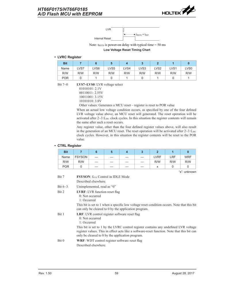
Rev. 1.50 5� ����st ��� �01� Rev. 1.50 59 ����st ��� �01�
HT66F0175/HT66F0185A/D Flash MCU with EEPROM
HT66F0175/HT66F0185A/D Flash MCU with EEPROM
LVR
Internal ResettRSTD + tSST
Note:tRSTDispower-ondelaywithtypicaltime=50msLow Voltage Reset Timing Chart
• LVRC Register
Bit 7 6 5 4 3 2 1 0Name LVS� LVS6 LVS5 LVS4 LVS3 LVS� LVS1 LVS0R/W R/W R/W R/W R/W R/W R/W R/W R/WPOR 0 1 0 1 0 1 0 1
Bit7~0 LVS7~LVS0:LVRvoltageselect01010101:2.1V00110011:2.55V10011001:3.15V10101010:3.8VOthervalues:GeneratesaMCUreset–registerisresettoPORvalue
Whenanactuallowvoltageconditionoccurs,asspecifiedbyoneofthefourdefinedLVRvoltagevalueabove,anMCUresetwillgenerated.Theresetoperationwillbeactivatedafter2~3fLIRCclockcycles.Inthissituationtheregistercontentswillremainthesameaftersucharesetoccurs.Anyregistervalue,otherthanthefourdefinedregistervaluesabove,willalsoresultinthegenerationofanMCUreset.Theresetoperationwillbeactivatedafter2~3fLIRCclockcycles.However,inthissituationtheregistercontentswillberesettothePORvalue.
• CTRL Register
Bit 7 6 5 4 3 2 1 0Name FSYSON — — — — LVRF LRF WRFR/W R/W — — — — R/W R/W R/WPOR 0 — — — — x 0 0
“x”: �nknownBit7 FSYSON:fSYSControlinIDLEMode
Describedelsewhere.Bit6~3 Unimplemented,readas“0”Bit2 LVRF:LVRfunctionresetflag
0:Notoccurred1:Occurred
Thisbitissetto1whenaspecificlowvoltageresetconditionoccurs.Notethatthisbitcanonlybeclearedto0bytheapplicationprogram.
Bit1 LRF:LVRcontrolregistersoftwareresetflag0:Notoccurred1:Occurred
Thisbitissetto1bytheLVRCcontrolregistercontainsanyundefinedLVRvoltageregistervalues.Thisineffectactslikeasoftware-resetfunction.Notethatthisbitcanonlybeclearedto0bytheapplicationprogram.
Bit0 WRF:WDTcontrolregistersoftwareresetflagDescribedelsewhere.
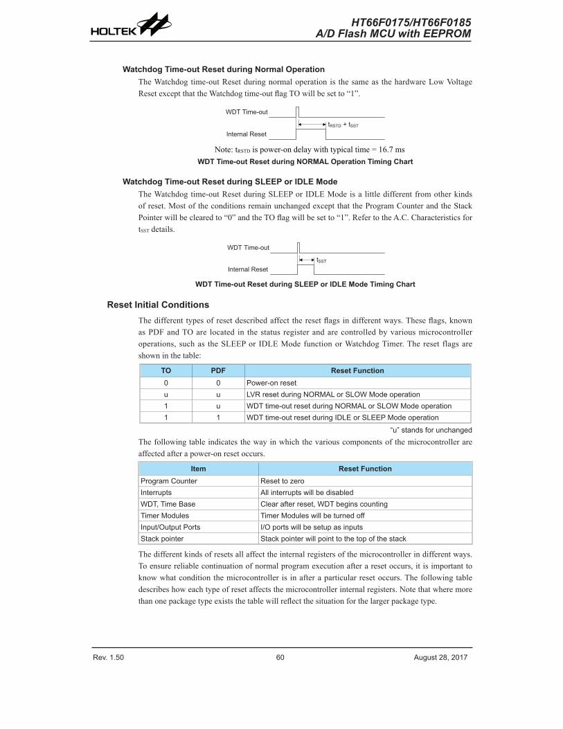
Rev. 1.50 60 ����st ��� �01� Rev. 1.50 61 ����st ��� �01�
HT66F0175/HT66F0185A/D Flash MCU with EEPROM
HT66F0175/HT66F0185A/D Flash MCU with EEPROM
Watchdog Time-out Reset during Normal OperationTheWatchdogtime-outResetduringnormaloperationis thesameas thehardwareLowVoltageResetexceptthattheWatchdogtime-outflagTOwillbesetto“1”.
WDT Time-o�t
Internal ResettRSTD + tSST
Note:tRSTDispower-ondelaywithtypicaltime=16.7msWDT Time-out Reset during NORMAL Operation Timing Chart
Watchdog Time-out Reset during SLEEP or IDLE ModeTheWatchdogtime-outResetduringSLEEPorIDLEModeisa littledifferentfromotherkindsofreset.MostoftheconditionsremainunchangedexceptthattheProgramCounterandtheStackPointerwillbeclearedto“0”andtheTOflagwillbesetto“1”.RefertotheA.C.CharacteristicsfortSSTdetails.
WDT Time-o�t
Internal ResettSST
WDT Time-out Reset during SLEEP or IDLE Mode Timing Chart
Reset Initial ConditionsThedifferent typesofresetdescribedaffect theresetflagsindifferentways.Theseflags,knownasPDFandTOare located in thestatus registerandarecontrolledbyvariousmicrocontrolleroperations,suchas theSLEEPorIDLEModefunctionorWatchdogTimer.Thereset flagsareshowninthetable:
TO PDF Reset Function0 0 Power-on reset� � LVR reset d�rin� NORM�L or SLOW Mode operation1 � WDT time-o�t reset d�rin� NORM�L or SLOW Mode operation1 1 WDT time-o�t reset d�rin� IDLE or SLEEP Mode operation
“�” stands for �nchan�edThefollowingtableindicatesthewayinwhichthevariouscomponentsofthemicrocontrollerareaffectedafterapower-onresetoccurs.
Item Reset FunctionPro�ram Co�nter Reset to zeroInterr�pts �ll interr�pts will be disabledWDT� Time Base Clear after reset� WDT be�ins co�ntin�Timer Mod�les Timer Mod�les will be t�rned offInp�t/O�tp�t Ports I/O ports will be set�p as inp�tsStack pointer Stack pointer will point to the top of the stack
Thedifferentkindsofresetsallaffecttheinternalregistersofthemicrocontrollerindifferentways.Toensurereliablecontinuationofnormalprogramexecutionafteraresetoccurs,itisimportanttoknowwhatconditionthemicrocontrolleris inafteraparticularresetoccurs.Thefollowingtabledescribeshoweachtypeofresetaffectsthemicrocontrollerinternalregisters.Notethatwheremorethanonepackagetypeexiststhetablewillreflectthesituationforthelargerpackagetype.

Rev. 1.50 60 ����st ��� �01� Rev. 1.50 61 ����st ��� �01�
HT66F0175/HT66F0185A/D Flash MCU with EEPROM
HT66F0175/HT66F0185A/D Flash MCU with EEPROM
Register
HT66F0175
HT66F0185
Reset(Power On)
LVR Reset(Normal Operation)
WDT Time-out(Normal Operation)
WDT Time-out(IDLE or SLEEP)*
MP0 ● ● x x x x x x x x x x x x x x x x x x x x x x x x � � � � � � � �MP1 ● ● x x x x x x x x x x x x x x x x x x x x x x x x � � � � � � � �BP ● ● - - - - - - - 0 - - - - - - - 0 - - - - - - - 0 - - - - - - - ��CC ● ● x x x x x x x x � � � � � � � � � � � � � � � � � � � � � � � �PCL ● ● 0 0 0 0 0 0 0 0 0 0 0 0 0 0 0 0 0 0 0 0 0 0 0 0 0 0 0 0 0 0 0 0TBLP ● ● x x x x x x x x � � � � � � � � � � � � � � � � � � � � � � � �TBLH ● ● x x x x x x x x � � � � � � � � � � � � � � � � � � � � � � � �TBHP ● - - - - - x x x - - - - - � � � - - - - - � � � - - - - - � � �TBHP ● - - - - x x x x - - - - � � � � - - - - � � � � - - - - � � � �ST�TUS ● ● - - 0 0 x x x x - - � � � � � � - - 1 � � � � � - - 1 1 � � � �SMOD ● ● 0 0 0 0 0 0 11 0 0 0 0 0 0 11 0 0 0 0 0 0 11 � � � � � � � �LVDC ● ● - - 0 0 - 0 0 0 - - 0 0 - 0 0 0 - - 0 0 - 0 0 0 - - � � - � � �INTEG ● ● - - - - 0 0 0 0 - - - - 0 0 0 0 - - - - 0 0 0 0 - - - - � � � �INTC0 ● - 0 - 0 0 - 0 0 - 0 - 0 0 - 0 0 - 0 - 0 0 - 0 0 - � - � � - � �INTC0 ● - 0 0 0 0 0 0 0 - 0 0 0 0 0 0 0 - 0 0 0 0 0 0 0 - � � � � � � �INTC1 ● ● 0 0 0 0 0 0 0 0 0 0 0 0 0 0 0 0 0 0 0 0 0 0 0 0 � � � � � � � �INTC� ● - 0 0 0 - 0 0 0 - 0 0 0 - 0 0 0 - 0 0 0 - 0 0 0 - � � � - � � �INTC� ● 0 0 0 0 0 0 0 0 0 0 0 0 0 0 0 0 0 0 0 0 0 0 0 0 � � � � � � � �MFI0 ● ● - - 0 0 - - 0 0 - - 0 0 - - 0 0 - - 0 0 - - 0 0 - - � � - - � �MFI1 ● ● 0 0 0 0 0 0 0 0 0 0 0 0 0 0 0 0 0 0 0 0 0 0 0 0 � � � � � � � �MFI� ● ● - - 0 0 - - 0 0 - - 0 0 - - 0 0 - - 0 0 - - 0 0 - - � � - - � �P� ● ● 1 1 1 1 1 1 1 1 1 1 1 1 1 1 1 1 1 1 1 1 1 1 1 1 � � � � � � � �P�C ● ● 1 1 1 1 1 1 1 1 1 1 1 1 1 1 1 1 1 1 1 1 1 1 1 1 � � � � � � � �P�PU ● ● 0 0 0 0 0 0 0 0 0 0 0 0 0 0 0 0 0 0 0 0 0 0 0 0 � � � � � � � �P�WU ● ● 0 0 0 0 0 0 0 0 0 0 0 0 0 0 0 0 0 0 0 0 0 0 0 0 � � � � � � � �TMPC ● 0 - - - - - 0 0 0 - - - - - 0 0 0 - - - - - 0 0 � - - - - - � �TMPC ● 0 - - - - 0 0 0 0 - - - - 0 0 0 0 - - - - 0 0 0 � - - - - � � �WDTC ● ● 0 1 0 1 0 0 11 0 1 0 1 0 0 11 0 1 0 1 0 0 11 � � � � � � � �TBC ● ● 0 0 11 0 111 0 0 11 0 111 0 0 11 0 111 � � � � � � � �CTRL ● ● 0 - - - - x 0 0 0 - - - - 0 0 0 0 - - - - 0 0 0 � - - - - � � �LVRC ● ● 0 1 0 1 0 1 0 1 0 1 0 1 0 1 0 1 0 1 0 1 0 1 0 1 � � � � � � � �EE� ● - - 0 0 0 0 0 0 - - 0 0 0 0 0 0 - - 0 0 0 0 0 0 - - � � � � � �EE� ● - 0 0 0 0 0 0 0 - 0 0 0 0 0 0 0 - 0 0 0 0 0 0 0 - � � � � � � �EED ● ● 0 0 0 0 0 0 0 0 0 0 0 0 0 0 0 0 0 0 0 0 0 0 0 0 � � � � � � � �S�DOL (�DRFS=0) ● ● x x x x - - - - x x x x - - - - x x x x - - - - � � � � - - - -S�DOL (�DRFS=1) ● ● x x x x x x x x � � � � � � � � � � � � � � � � � � � � � � � �S�DOH (�DRFS=0) ● ● x x x x x x x x � � � � � � � � � � � � � � � � � � � � � � � �
S�DOH (�DRFS=1) ● ● - - - - x x x x - - - - � � � � - - - - � � � � - - - - � � � �
S�DC0 ● ● 0 0 0 0 - 0 0 0 0 0 0 0 - 0 0 0 0 0 0 0 - 0 0 0 � � � � - � � �S�DC1 ● ● 0 0 0 - - 0 0 0 0 0 0 - - 0 0 0 0 0 0 - - 0 0 0 � � � - - � � �S�DC� ● ● 0 0 0 0 0 0 0 0 0 0 0 0 0 0 0 0 0 0 0 0 0 0 0 0 � � � � � � � �PB ● ● - 1 1 1 1 1 1 1 - 1 1 1 1 1 1 1 - 1 1 1 1 1 1 1 - � � � � � � �PBC ● ● - 1 1 1 1 1 1 1 - 1 1 1 1 1 1 1 - 1 1 1 1 1 1 1 - � � � � � � �

Rev. 1.50 6� ����st ��� �01� Rev. 1.50 63 ����st ��� �01�
HT66F0175/HT66F0185A/D Flash MCU with EEPROM
HT66F0175/HT66F0185A/D Flash MCU with EEPROM
Register
HT66F0175
HT66F0185
Reset(Power On)
LVR Reset(Normal Operation)
WDT Time-out(Normal Operation)
WDT Time-out(IDLE or SLEEP)*
PBPU ● ● - 0 0 0 0 0 0 0 - 0 0 0 0 0 0 0 - 0 0 0 0 0 0 0 - � � � � � � �TM�C0 ● 0 0 0 0 0 - - - 0 0 0 0 0 - - - 0 0 0 0 0 - - - � � � � � - - -TM�C1 ● 0 0 0 0 0 0 0 0 0 0 0 0 0 0 0 0 0 0 0 0 0 0 0 0 � � � � � � � �TM�DL ● 0 0 0 0 0 0 0 0 0 0 0 0 0 0 0 0 0 0 0 0 0 0 0 0 � � � � � � � �TM�DH ● 0 0 0 0 0 0 0 0 0 0 0 0 0 0 0 0 0 0 0 0 0 0 0 0 � � � � � � � �TM��L ● 0 0 0 0 0 0 0 0 0 0 0 0 0 0 0 0 0 0 0 0 0 0 0 0 � � � � � � � �TM��H ● 0 0 0 0 0 0 0 0 0 0 0 0 0 0 0 0 0 0 0 0 0 0 0 0 � � � � � � � �TM�RP ● 0 0 0 0 0 0 0 0 0 0 0 0 0 0 0 0 0 0 0 0 0 0 0 0 � � � � � � � �TM0C0 ● 0 0 0 0 0 - - - 0 0 0 0 0 - - - 0 0 0 0 0 - - - � � � � � - - -TM0C1 ● 0 0 0 0 0 0 0 0 0 0 0 0 0 0 0 0 0 0 0 0 0 0 0 0 � � � � � � � �TM0DL ● 0 0 0 0 0 0 0 0 0 0 0 0 0 0 0 0 0 0 0 0 0 0 0 0 � � � � � � � �TM0DH ● - - - - - - - 0 0 - - - - - - 0 0 - - - - - - 0 0 - - - - - - � �TM0�L ● 0 0 0 0 0 0 0 0 0 0 0 0 0 0 0 0 0 0 0 0 0 0 0 0 � � � � � � � �TM0�H ● - - - - - - - 0 0 - - - - - - 0 0 - - - - - - 0 0 - - - - - - � �TM0RPL ● 0 0 0 0 0 0 0 0 0 0 0 0 0 0 0 0 0 0 0 0 0 0 0 0 � � � � � � � �TM0RPH ● - - - - - - - 0 0 - - - - - - 0 0 - - - - - - 0 0 - - - - - - � �TM0C0 ● 0 0 0 0 0 - - - 0 0 0 0 0 - - - 0 0 0 0 0 - - - � � � � � - - -TM0C1 ● 0 0 0 0 0 0 0 0 0 0 0 0 0 0 0 0 0 0 0 0 0 0 0 0 � � � � � � � �TM0DL ● 0 0 0 0 0 0 0 0 0 0 0 0 0 0 0 0 0 0 0 0 0 0 0 0 � � � � � � � �TM0DH ● 0 0 0 0 0 0 0 0 0 0 0 0 0 0 0 0 0 0 0 0 0 0 0 0 � � � � � � � �TM0�L ● 0 0 0 0 0 0 0 0 0 0 0 0 0 0 0 0 0 0 0 0 0 0 0 0 � � � � � � � �TM0�H ● 0 0 0 0 0 0 0 0 0 0 0 0 0 0 0 0 0 0 0 0 0 0 0 0 � � � � � � � �TM0RP ● 0 0 0 0 0 0 0 0 0 0 0 0 0 0 0 0 0 0 0 0 0 0 0 0 � � � � � � � �TM1C0 ● ● 0 0 0 0 0 - - - 0 0 0 0 0 - - - 0 0 0 0 0 - - - � � � � � - - -TM1C1 ● ● 0 0 0 0 0 0 0 0 0 0 0 0 0 0 0 0 0 0 0 0 0 0 0 0 � � � � � � � �TM1DL ● ● 0 0 0 0 0 0 0 0 0 0 0 0 0 0 0 0 0 0 0 0 0 0 0 0 � � � � � � � �TM1DH ● ● - - - - - - - 0 0 - - - - - - 0 0 - - - - - - 0 0 - - - - - - � �TM1�L ● ● 0 0 0 0 0 0 0 0 0 0 0 0 0 0 0 0 0 0 0 0 0 0 0 0 � � � � � � � �TM1�H ● ● - - - - - - - 0 0 - - - - - - 0 0 - - - - - - 0 0 - - - - - - � �TM1RPL ● ● 0 0 0 0 0 0 0 0 0 0 0 0 0 0 0 0 0 0 0 0 0 0 0 0 � � � � � � � �TM1RPH ● ● - - - - - - - 0 0 - - - - - - 0 0 - - - - - - 0 0 - - - - - - � �CPC ● 1 0 0 0 0 0 0 1 1 0 0 0 0 0 0 1 1 0 0 0 0 0 0 1 � � � � � � � �PC ● ● - 1 1 1 1 1 1 1 - 1 1 1 1 1 1 1 - 1 1 1 1 1 1 1 - � � � � � � �PCC ● ● - 1 1 1 1 1 1 1 - 1 1 1 1 1 1 1 - 1 1 1 1 1 1 1 - � � � � � � �PCPU ● ● - 0 0 0 0 0 0 0 - 0 0 0 0 0 0 0 - 0 0 0 0 0 0 0 - � � � � � � ��CERL ● ● 1 1 1 1 1 1 1 1 1 1 1 1 1 1 1 1 1 1 1 1 1 1 1 1 � � � � � � � �SIMC0 ● ● 111 - 0 0 0 0 111 - 0 0 0 0 111 - 0 0 0 0 � � � - � � � �SIMC1 ● ● 1 0 0 0 0 0 0 1 1 0 0 0 0 0 0 1 1 0 0 0 0 0 0 1 � � � � � � � �SIMD ● ● x x x x x x x x x x x x x x x x x x x x x x x x � � � � � � � �SIM�/SIMC� ● ● 0 0 0 0 0 0 0 0 0 0 0 0 0 0 0 0 0 0 0 0 0 0 0 0 � � � � � � � �SIMTOC ● ● 0 0 0 0 0 0 0 0 0 0 0 0 0 0 0 0 0 0 0 0 0 0 0 0 � � � � � � � �SLCDC0 ● ● 0 0 0 0 0 0 0 0 0 0 0 0 0 0 0 0 0 0 0 0 0 0 0 0 � � � � � � � �SLCDC1 ● ● 0 0 0 0 0 0 0 0 0 0 0 0 0 0 0 0 0 0 0 0 0 0 0 0 � � � � � � � �SLCDC� ● ● 0 0 0 0 0 0 0 0 0 0 0 0 0 0 0 0 0 0 0 0 0 0 0 0 � � � � � � � �

Rev. 1.50 6� ����st ��� �01� Rev. 1.50 63 ����st ��� �01�
HT66F0175/HT66F0185A/D Flash MCU with EEPROM
HT66F0175/HT66F0185A/D Flash MCU with EEPROM
Register
HT66F0175
HT66F0185
Reset(Power On)
LVR Reset(Normal Operation)
WDT Time-out(Normal Operation)
WDT Time-out(IDLE or SLEEP)*
SLCDC3 ● ● 0 0 0 0 0 0 0 0 0 0 0 0 0 0 0 0 0 0 0 0 0 0 0 0 � � � � � � � �SLCDC4 ● - - - - - - 0 0 - - - - - - 0 0 - - - - - - 0 0 - - - - - - � �SLEDC0 ● ● 0 1 0 1 0 1 0 1 0 1 0 1 0 1 0 1 0 1 0 1 0 1 0 1 � � � � � � � �SLEDC1 ● - - 0 1 0 1 0 1 - - 0 1 0 1 0 1 - - 0 1 0 1 0 1 - - � � � � � �SLEDC1 ● - - - - 0 1 0 1 - - - - 0 1 0 1 - - - - 0 1 0 1 - - - - � � � �IFS ● - - 0 0 0 0 0 0 - - 0 0 0 0 0 0 - - 0 0 0 0 0 0 - - � � � � � �IFS ● - 0 0 0 0 0 0 0 - 0 0 0 0 0 0 0 - 0 0 0 0 0 0 0 - � � � � � � �PD ● - - - - 1 1 1 1 - - - - 1 1 1 1 - - - - 1 1 1 1 - - - - � � � �PDC ● - - - - 1 1 1 1 - - - - 1 1 1 1 - - - - 1 1 1 1 - - - - � � � �PDPU ● - - - - 0 0 0 0 - - - - 0 0 0 0 - - - - 0 0 0 0 - - - - � � � �USR ● 0 0 0 0 1 0 11 0 0 0 0 1 0 11 0 0 0 0 1 0 11 � � � � � � � �UCR1 ● 0 0 0 0 0 0 x 0 0 0 0 0 0 0 x 0 0 0 0 0 0 0 x 0 � � � � � � � �UCR� ● 0 0 0 0 0 0 0 0 0 0 0 0 0 0 0 0 0 0 0 0 0 0 0 0 � � � � � � � �BRG ● x x x x x x x x x x x x x x x x x x x x x x x x � � � � � � � �TXR_RXR ● x x x x x x x x x x x x x x x x x x x x x x x x � � � � � � � �EEC ● ● - - - - 0 0 0 0 - - - - 0 0 0 0 - - - - 0 0 0 0 - - - - � � � �
Note:“u”standsforunchanged“x”standsfor“unknown”“-“standsforunimplemented

Rev. 1.50 64 ����st ��� �01� Rev. 1.50 65 ����st ��� �01�
HT66F0175/HT66F0185A/D Flash MCU with EEPROM
HT66F0175/HT66F0185A/D Flash MCU with EEPROM
Input/Output PortsHoltekmicrocontrollersofferconsiderableflexibilityontheirI/Oports.Withtheinputoroutputdesignationofeverypinfullyunderuserprogramcontrol,pull-highselectionsforallportsandwake-upselectionsoncertainpins,theuserisprovidedwithanI/Ostructuretomeettheneedsofawiderangeofapplicationpossibilities.
Thesedevicesprovidebidirectionalinput/outputlineslabeledwithportnamesPA~PD.TheseI/OportsaremappedtotheRAMDataMemorywithspecificaddressesasshownintheSpecialPurposeDataMemorytable.Allof theseI/Oportscanbeusedforinputandoutputoperations.Forinputoperation,theseportsarenon-latching,whichmeanstheinputsmustbereadyattheT2risingedgeofinstruction“MOVA,[m]”,wheremdenotestheportaddress.Foroutputoperation,allthedataislatchedandremainsunchangeduntiltheoutputlatchisrewritten.
Register Name
Bit
7 6 5 4 3 2 1 0P�WU P�WU� P�WU6 P�WU5 P�WU4 P�WU3 P�WU� P�WU1 P�WU0
P� P�� P�6 P�5 P�4 P�3 P�� P�1 P�0P�C P�C� P�C6 P�C5 P�C4 P�C3 P�C� P�C1 P�C0
P�PU P�PU� P�PU6 P�PU5 P�PU4 P�PU3 P�PU� P�PU1 P�PU0PB — PB6 PB5 PB4 PB3 PB� PB1 PB0
PBC — PBC6 PBC5 PBC4 PBC3 PBC� PBC1 PBC0PBPU — PBPU6 PBPU5 PBPU4 PBPU3 PBPU� PBPU1 PBPU0
PC — PC6 PC5 PC4 PC3 PC� PC1 PC0PCC — PCC6 PCC5 PCC4 PCC3 PCC� PCC1 PCC0
PCPU — PCPU6 PCPU5 PCPU4 PCPU3 PCPU� PCPU1 PCPU0
I/O Registers List – HT66F0175

Rev. 1.50 64 ����st ��� �01� Rev. 1.50 65 ����st ��� �01�
HT66F0175/HT66F0185A/D Flash MCU with EEPROM
HT66F0175/HT66F0185A/D Flash MCU with EEPROM
Register Name
Bit
7 6 5 4 3 2 1 0P�WU P�WU� P�WU6 P�WU5 P�WU4 P�WU3 P�WU� P�WU1 P�WU0
P� P�� P�6 P�5 P�4 P�3 P�� P�1 P�0P�C P�C� P�C6 P�C5 P�C4 P�C3 P�C� P�C1 P�C0
P�PU P�PU� P�PU6 P�PU5 P�PU4 P�PU3 P�PU� P�PU1 P�PU0PB — PB6 PB5 PB4 PB3 PB� PB1 PB0
PBC — PBC6 PBC5 PBC4 PBC3 PBC� PBC1 PBC0PBPU — PBPU6 PBPU5 PBPU4 PBPU3 PBPU� PBPU1 PBPU0
PC — PC6 PC5 PC4 PC3 PC� PC1 PC0PCC — PCC6 PCC5 PCC4 PCC3 PCC� PCC1 PCC0
PCPU — PCPU6 PCPU5 PCPU4 PCPU3 PCPU� PCPU1 PCPU0PD — — — — PD3 PD� PD1 PD0
PDC — — — — PDC3 PDC� PDC1 PDC0PDPU — — — — PDPU3 PDPU� PDPU1 PDPU0
I/O Registers List – HT66F0185
“—”:Unimplemented,readas“0”.PAWUn:PortAPinwake-upfunctioncontrol
0:Disable1:Enable
PAPUn/PBPUn/PCPUn/PDPUn:I/OPinpull-highfunctioncontrol0:Disable1:Enable
PAn/PBn/PCn/PDn:I/OPortDatabit0:Data01:Data1
PACn/PBCn/PCCn/PDCn:I/OPintypeselection0:Output1:Input
Pull-high ResistorsManyproductapplicationsrequirepull-highresistorsfortheirswitchinputsusuallyrequiringtheuseofanexternal resistor.Toeliminate theneedfor theseexternal resistors,all I/Opins,whenconfiguredasaninputhavethecapabilityofbeingconnectedtoaninternalpull-highresistor.Thesepull-highresistorsareselectedusingtherelevantpull-highcontrolregistersandareimplementedusingweakPMOStransistors.
Port A Wake-upTheHALTinstructionforcesthemicrocontrollerintotheSLEEPorIDLEModewhichpreservespower,afeature that is importantforbatteryandother low-powerapplications.Variousmethodsexisttowake-upthemicrocontroller,oneofwhichistochangethelogicconditionononeofthePortApinsfromhightolow.Thisfunctionisespeciallysuitableforapplicationsthatcanbewokenupviaexternalswitches.EachpinonPortAcanbeselectedindividuallytohavethiswake-upfeatureusingthePAWUregister.

Rev. 1.50 66 ����st ��� �01� Rev. 1.50 6� ����st ��� �01�
HT66F0175/HT66F0185A/D Flash MCU with EEPROM
HT66F0175/HT66F0185A/D Flash MCU with EEPROM
I/O Port Control RegistersEachPorthas itsowncontrol register,knownasPAC~PDC,whichcontrols the input/outputconfiguration.With thiscontrolregister,eachI/Opinwithorwithoutpull-highresistorscanbereconfigureddynamicallyunder softwarecontrol.For the I/Opin to functionasan input, thecorrespondingbitofthecontrolregistermustbewrittenasa“1”.Thiswillthenallowthelogicstateoftheinputpintobedirectlyreadbyinstructions.Whenthecorrespondingbitofthecontrolregisteriswrittenasa“0”,theI/OpinwillbesetupasaCMOSoutput.Ifthepiniscurrentlysetupasanoutput,instructionscanstillbeusedtoreadtheoutputregister.
However,itshouldbenotedthattheprogramwillinfactonlyreadthestatusoftheoutputdatalatchandnottheactuallogicstatusoftheoutputpin.
I/O Port Source Current ControlThesedevices supportdifferent sourcecurrentdrivingcapability foreach I/Oport.With thecorrespondingselectionregister,SLEDC0andSLEDC1,eachI/Oportcansupportfourlevelsofthesourcecurrentdrivingcapability.UsersshouldrefertotheD.C.characteristicssectiontoselectthedesiredsourcecurrentfordifferentapplications.
Register Name
Bit
7 6 5 4 3 2 1 0SLEDC0 PBPS3 PBPS� PBPS1 PBPS0 P�PS3 P�PS� P�PS1 P�PS0SLEDC1 (HT66F01�5) — — — — PCPS3 PCPS� PCPS1 PCPS0
SLEDC1 (HT66F01�5) — — PDPS1 PDPS0 PCPS3 PCPS� PCPS1 PCPS0
I/O Port Source Current Control Registers List
SLEDC0 Register
Bit 7 6 5 4 3 2 1 0Name PBPS3 PBPS� PBPS1 PBPS0 P�PS3 P�PS� P�PS1 P�PS0R/W R/W R/W R/W R/W R/W R/W R/W R/WPOR 0 1 0 1 0 1 0 1
Bit7~6 PBPS3~PBPS2:PB6~PB4sourcecurrentselection00:sourcecurrent=Level0(min.)01:sourcecurrent=Level110:sourcecurrent=Level211:sourcecurrent=Level3(max.)
Bit5~4 PBPS1~PBPS0:PB3~PB0sourcecurrentselection00:sourcecurrent=Level0(min.)01:sourcecurrent=Level110:sourcecurrent=Level211:sourcecurrent=Level3(max.)
Bit3~2 PAPS3~PAPS2:PA7~PA4sourcecurrentselection00:sourcecurrent=Level0(min.)01:sourcecurrent=Level110:sourcecurrent=Level211:sourcecurrent=Level3(max.)
Bit1~0 PAPS1~PAPS0:PA3~PA0sourcecurrentselection00:sourcecurrent=Level0(min.)01:sourcecurrent=Level110:sourcecurrent=Level211:sourcecurrent=Level3(max.)
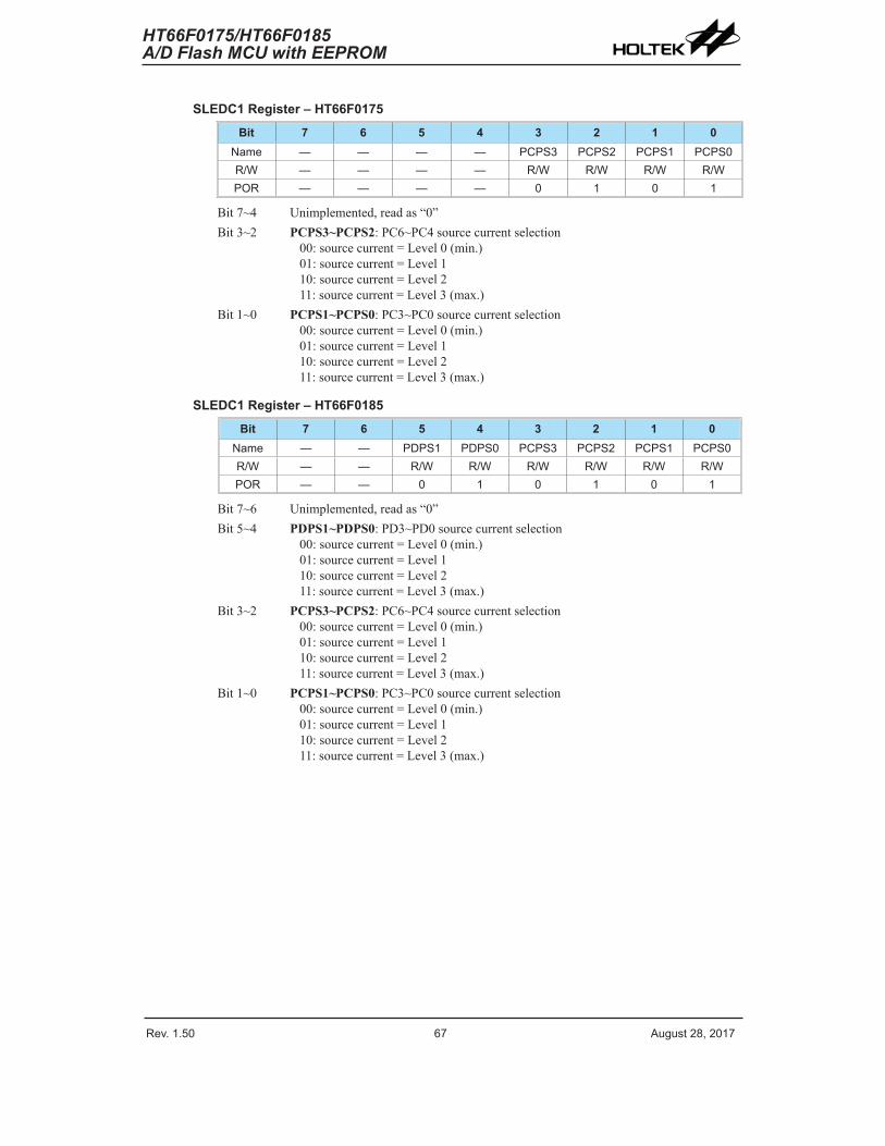
Rev. 1.50 66 ����st ��� �01� Rev. 1.50 6� ����st ��� �01�
HT66F0175/HT66F0185A/D Flash MCU with EEPROM
HT66F0175/HT66F0185A/D Flash MCU with EEPROM
SLEDC1 Register – HT66F0175
Bit 7 6 5 4 3 2 1 0Name — — — — PCPS3 PCPS� PCPS1 PCPS0R/W — — — — R/W R/W R/W R/WPOR — — — — 0 1 0 1
Bit7~4 Unimplemented,readas“0”Bit3~2 PCPS3~PCPS2:PC6~PC4sourcecurrentselection
00:sourcecurrent=Level0(min.)01:sourcecurrent=Level110:sourcecurrent=Level211:sourcecurrent=Level3(max.)
Bit1~0 PCPS1~PCPS0:PC3~PC0sourcecurrentselection00:sourcecurrent=Level0(min.)01:sourcecurrent=Level110:sourcecurrent=Level211:sourcecurrent=Level3(max.)
SLEDC1 Register – HT66F0185
Bit 7 6 5 4 3 2 1 0Name — — PDPS1 PDPS0 PCPS3 PCPS� PCPS1 PCPS0R/W — — R/W R/W R/W R/W R/W R/WPOR — — 0 1 0 1 0 1
Bit7~6 Unimplemented,readas“0”Bit5~4 PDPS1~PDPS0:PD3~PD0sourcecurrentselection
00:sourcecurrent=Level0(min.)01:sourcecurrent=Level110:sourcecurrent=Level211:sourcecurrent=Level3(max.)
Bit3~2 PCPS3~PCPS2:PC6~PC4sourcecurrentselection00:sourcecurrent=Level0(min.)01:sourcecurrent=Level110:sourcecurrent=Level211:sourcecurrent=Level3(max.)
Bit1~0 PCPS1~PCPS0:PC3~PC0sourcecurrentselection00:sourcecurrent=Level0(min.)01:sourcecurrent=Level110:sourcecurrent=Level211:sourcecurrent=Level3(max.)
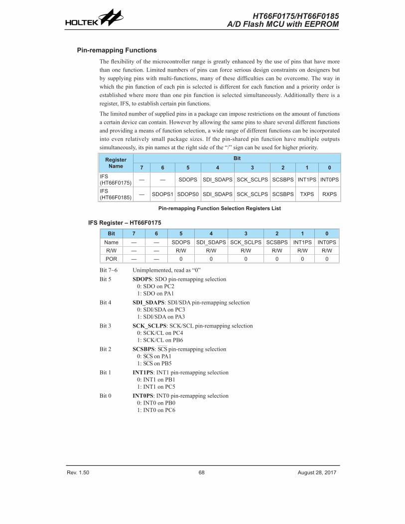
Rev. 1.50 6� ����st ��� �01� Rev. 1.50 69 ����st ��� �01�
HT66F0175/HT66F0185A/D Flash MCU with EEPROM
HT66F0175/HT66F0185A/D Flash MCU with EEPROM
Pin-remapping FunctionsTheflexibilityofthemicrocontrollerrangeisgreatlyenhancedbytheuseofpinsthathavemorethanonefunction.Limitednumbersofpinscanforceseriousdesignconstraintsondesignersbutbysupplyingpinswithmulti-functions,manyof thesedifficultiescanbeovercome.Thewayinwhichthepinfunctionofeachpinisselectedisdifferentforeachfunctionandapriorityorderisestablishedwheremorethanonepinfunctionisselectedsimultaneously.Additionally there isaregister,IFS,toestablishcertainpinfunctions.
Thelimitednumberofsuppliedpinsinapackagecanimposerestrictionsontheamountoffunctionsacertaindevicecancontain.Howeverbyallowingthesamepinstoshareseveraldifferentfunctionsandprovidingameansoffunctionselection,awiderangeofdifferentfunctionscanbeincorporatedintoeven relativelysmallpackagesizes. If thepin-sharedpin functionhavemultipleoutputssimultaneously,itspinnamesattherightsideofthe“/”signcanbeusedforhigherpriority.
Register Name
Bit
7 6 5 4 3 2 1 0IFS (HT66F01�5) — — SDOPS SDI_SD�PS SCK_SCLPS SCSBPS INT1PS INT0PS
IFS (HT66F01�5) — SDOPS1 SDOPS0 SDI_SD�PS SCK_SCLPS SCSBPS TXPS RXPS
Pin-remapping Function Selection Registers List
IFS Register – HT66F0175
Bit 7 6 5 4 3 2 1 0Name — — SDOPS SDI_SD�PS SCK_SCLPS SCSBPS INT1PS INT0PSR/W — — R/W R/W R/W R/W R/W R/WPOR — — 0 0 0 0 0 0
Bit7~6 Unimplemented,readas“0”Bit5 SDOPS:SDOpin-remappingselection
0:SDOonPC21:SDOonPA1
Bit4 SDI_SDAPS:SDI/SDApin-remappingselection0:SDI/SDAonPC31:SDI/SDAonPA3
Bit3 SCK_SCLPS:SCK/SCLpin-remappingselection0:SCK/CLonPC41:SCK/CLonPB6
Bit2 SCSBPS:SCSpin-remappingselection0:SCSonPA11:SCSonPB5
Bit1 INT1PS:INT1pin-remappingselection0:INT1onPB11:INT1onPC5
Bit0 INT0PS:INT0pin-remappingselection0:INT0onPB01:INT0onPC6

Rev. 1.50 6� ����st ��� �01� Rev. 1.50 69 ����st ��� �01�
HT66F0175/HT66F0185A/D Flash MCU with EEPROM
HT66F0175/HT66F0185A/D Flash MCU with EEPROM
IFS Register – HT66F0185
Bit 7 6 5 4 3 2 1 0Name — SDOPS1 SDOPS0 SDI_SD�PS SCK_SCLPS SCSBPS TXPS RXPSR/W — R/W R/W R/W R/W R/W R/W R/WPOR — 0 0 0 0 0 0 0
Bit7 Unimplemented,readas“0”Bit6~5 SDOPS1~SDOPS0:SDOpin-remappingselection
00:SDOonPC301:SDOonPA110:Undefined11:SDOonPC2
Bit4 SDI_SDAPS:SDI/SDApin-remappingselection0:SDI/SDAonPC41:SDI/SDAonPA3
Bit3 SCK_SCLPS:SCK/SCLpin-remappingselection0:SCK/CLonPC51:SCK/CLonPB6
Bit2 SCSBPS:SCSpin-remappingselection0:SCSonPC61:SCSonPB5
Bit1 TXPS:TXpin-remappingselection0:TXonPD21:TXonPB3
Bit0 RXPS:RXpin-remappingselection0:RXonPD11:RXonPB4
I/O Pin StructuresTheaccompanyingdiagrams illustrate the internalstructuresofsomegeneric I/Opin types.AstheexactlogicalconstructionoftheI/Opinwilldifferfromthesedrawings,theyaresuppliedasaguideonlytoassistwiththefunctionalunderstandingoftheI/Opins.Thewiderangeofpin-sharedstructuresdoesnotpermitalltypestobeshown.
� � �
���
� � � � � � � � � � � � � �� � � � � � � � � � � � �
� � � � � � � � � � � � � � �
� �
� ��
� �
� ��
� � � � � � � � � � �� � � � � � �
� � � � � � � � � � � � � � � � � � � �
� � � � � � � � �
� � � � � � � � � � � � � � � � � �
� � � � � � � � � � � � � � � � �
� � � � � � � �
� � � � � � �
�
�
� � � � � � �
� � � �� � � � � � �
� � � � � � �� � � � � �� � � � � �
Generic Input/Output Structure
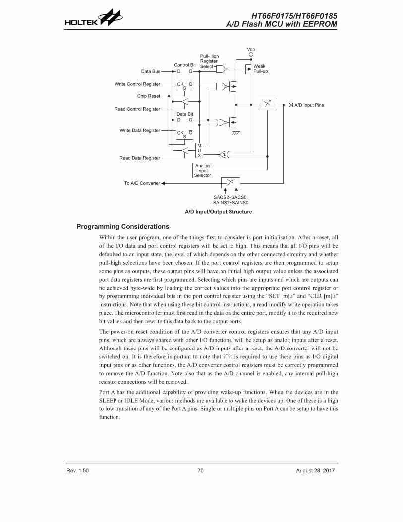
Rev. 1.50 �0 ����st ��� �01� Rev. 1.50 �1 ����st ��� �01�
HT66F0175/HT66F0185A/D Flash MCU with EEPROM
HT66F0175/HT66F0185A/D Flash MCU with EEPROM
� � �
���� � � � � � � � � � � � � � � � � �
� � � � � � � � � �� � � � � � � �
� � � � � � � � � � � � � � � � � � � �
� � � � � � � � �
� � � � � � � � � � � � � � � � � � � �
� � � � � � � � � � � � � � � � � �
� � � � � � � �
� � � � � � � � � � � � � �
� � � � � � � � � � � � �� � � � � � � � � � � � �
� � � � � � � � � � � � � � � �
� � �� � � �
� � � � �� � � � �
� � � � � �
� �
� ��
�
� �
� ��
�
� � � � � � � � � � � � �� � � �
A/D Input/Output Structure
Programming ConsiderationsWithintheuserprogram,oneof thethingsfirst toconsider isport initialisation.Afterareset,allof theI/Odataandportcontrolregisterswillbeset tohigh.ThismeansthatallI/Opinswillbedefaultedtoaninputstate,thelevelofwhichdependsontheotherconnectedcircuitryandwhetherpull-highselectionshavebeenchosen.If theportcontrolregistersarethenprogrammedtosetupsomepinsasoutputs,theseoutputpinswillhaveaninitialhighoutputvalueunlesstheassociatedportdataregistersarefirstprogrammed.Selectingwhichpinsareinputsandwhichareoutputscanbeachievedbyte-widebyloadingthecorrectvalues into theappropriateportcontrolregisterorbyprogrammingindividualbitsintheportcontrolregisterusingthe“SET[m].i”and“CLR[m].i”instructions.Notethatwhenusingthesebitcontrolinstructions,aread-modify-writeoperationtakesplace.Themicrocontrollermustfirstreadinthedataontheentireport,modifyittotherequirednewbitvaluesandthenrewritethisdatabacktotheoutputports.
Thepower-onresetconditionof theA/Dconvertercontrolregistersensures thatanyA/Dinputpins,whicharealwayssharedwithotherI/Ofunctions,willbesetupasanaloginputsafterareset.AlthoughthesepinswillbeconfiguredasA/Dinputsafterareset, theA/Dconverterwillnotbeswitchedon.It is thereforeimportant tonotethat if it isrequiredtousethesepinsasI/Odigitalinputpinsorasotherfunctions,theA/DconvertercontrolregistersmustbecorrectlyprogrammedtoremovetheA/Dfunction.Notealsothatas theA/Dchannelisenabled,anyinternalpull-highresistorconnectionswillberemoved.
PortAhastheadditionalcapabilityofprovidingwake-upfunctions.WhenthedevicesareintheSLEEPorIDLEMode,variousmethodsareavailabletowakethedevicesup.OneoftheseisahightolowtransitionofanyofthePortApins.SingleormultiplepinsonPortAcanbesetuptohavethisfunction.

Rev. 1.50 �0 ����st ��� �01� Rev. 1.50 �1 ����st ��� �01�
HT66F0175/HT66F0185A/D Flash MCU with EEPROM
HT66F0175/HT66F0185A/D Flash MCU with EEPROM
Timer Modules – TMOneofthemostfundamentalfunctionsinanymicrocontrollerdevicesistheabilitytocontrolandmeasuretime.Toimplement timerelatedfunctionseachdeviceincludesseveralTimerModules,generallyabbreviatedtothenameTM.TheTMsaremulti-purposetimingunitsandservetoprovideoperationssuchasTimer/Counter,InputCapture,CompareMatchOutputandSinglePulseOutputaswellasbeingthefunctionalunitforthegenerationofPWMsignals.EachoftheTMshastwointerrupts.TheadditionofinputandoutputpinsforeachTMensuresthatusersareprovidedwithtimingunitswithawideandflexiblerangeoffeatures.
ThecommonfeaturesofthedifferentTMtypesaredescribedherewithmoredetailedinformationprovidedintheindividualCompact,StandardandPeriodicTMsections.
IntroductionThedevicescontain twoor threeTMsdependinguponwhichdevice isselectedwitheachTMhavingareferencenameofTM0,TM1,andTM2.Each individualTMcanbecategorisedasacertaintype,namelyCompactTypeTM,StandardTypeTMorPeriodicTypeTM.Althoughsimilarinnature,thedifferentTMtypesvaryintheirfeaturecomplexity.ThecommonfeaturestoalloftheCompact,StandardandPeriodicTMswillbedescribedinthissectionandthedetailedoperationregardingeachof theTMtypeswillbedescribed inseparatesections.Themain featuresanddifferencesbetweenthethreetypesofTMsaresummarisedintheaccompanyingtable.
TM Function CTM STM PTMTimer/Co�nter √ √ √Inp�t Capt�re — √ √Compare Match O�tp�t √ √ √PWM Channels 1 1 1Sin�le P�lse O�tp�t — 1 1PWM �li�nment Ed�e Ed�e Ed�ePWM �dj�stment Period & D�ty D�ty or Period D�ty or Period D�ty or Period
TM Function Summary
EachdeviceintheseriescontainsaspecificnumberofeitherCompactType,StandardTypeandPeriodicTypeTMunitswhichareshowninthetabletogetherwiththeirindividualreferencename,TM0~TM2.
Device TM0 TM1 TM2HT66F01�5 10-bit PTM 10-bit PTM —HT66F01�5 16-bit STM 10-bit PTM 16-bit CTM
TM Name/Type Reference
TM OperationThedifferenttypesofTMofferadiverserangeoffunctions,fromsimpletimingoperationstoPWMsignalgeneration.ThekeytounderstandinghowtheTMoperates is tosee it in termsofafreerunningcount-upcounterwhosevalueisthencomparedwiththevalueofpre-programmedinternalcomparators.Whenthefreerunningcount-upcounterhasthesamevalueasthepre-programmedcomparator,knownasacomparematchsituation,aTMinterruptsignalwillbegeneratedwhichcanclearthecounterandperhapsalsochangetheconditionoftheTMoutputpin.TheinternalTMcounterisdrivenbyauserselectableclocksource,whichcanbeaninternalclockoranexternalpin.
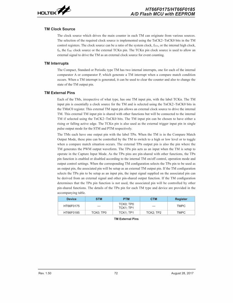
Rev. 1.50 �� ����st ��� �01� Rev. 1.50 �3 ����st ��� �01�
HT66F0175/HT66F0185A/D Flash MCU with EEPROM
HT66F0175/HT66F0185A/D Flash MCU with EEPROM
TM Clock SourceTheclocksourcewhichdrives themaincounter ineachTMcanoriginatefromvarioussources.TheselectionoftherequiredclocksourceisimplementedusingtheTnCK2~TnCK0bitsintheTMcontrolregisters.Theclocksourcecanbearatioofthesystemclock,fSYS,ortheinternalhighclock,fH,thefTBCclocksourceortheexternalTCKnpin.TheTCKnpinclocksourceisusedtoallowanexternalsignaltodrivetheTMasanexternalclocksourceforeventcounting.
TM InterruptsTheCompact,StandardorPeriodictypeTMhastwointernalinterrupts,oneforeachoftheinternalcomparatorAorcomparatorP,whichgenerateaTMinterruptwhenacomparematchconditionoccurs.WhenaTMinterruptisgenerated,itcanbeusedtoclearthecounterandalsotochangethestateoftheTMoutputpin.
TM External PinsEachoftheTMs,irrespectiveofwhattype,hasoneTMinputpin,withthelabelTCKn.TheTMinputpinisessentiallyaclocksourcefortheTMandisselectedusingtheTnCK2~TnCK0bitsintheTMnC0register.ThisexternalTMinputpinallowsanexternalclocksourcetodrivetheinternalTM.ThisexternalTMinputpinissharedwithotherfunctionsbutwillbeconnectedtotheinternalTMifselectedusingtheTnCK2~TnCK0bits.TheTMinputpincanbechosentohaveeitherarisingorfallingactiveedge.TheTCKnpinisalsousedastheexternaltriggerinputpininsinglepulseoutputmodefortheSTMandPTMrespectively.
TheTMseachhaveoneoutputpinwith the labelTPn.WhentheTMis in theCompareMatchOutputMode,thesepinscanbecontrolledbytheTMtoswitchtoahighorlowlevelortotogglewhenacomparematchsituationoccurs.TheexternalTPnoutputpin isalso thepinwhere theTMgeneratesthePWMoutputwaveform.TheTPnpinactsasaninputwhentheTMissetuptooperateintheCaptureInputMode.AstheTPnpinsarepin-sharedwithotherfunctions,theTPnpinfunctionisenabledordisabledaccordingtotheinternalTMon/offcontrol,operationmodeandoutputcontrolsettings.WhenthecorrespondingTMconfigurationselectstheTPnpintobeusedasanoutputpin,theassociatedpinwillbesetupasanexternalTMoutputpin.IftheTMconfigurationselectstheTPnpintobesetupasaninputpin,theinputsignalsuppliedontheassociatedpincanbederivedfromanexternalsignalandotherpin-sharedoutputfunction.If theTMconfigurationdetermines that theTPnpinfunction isnotused, theassociatedpinwillbecontrolledbyotherpin-sharedfunctions.ThedetailsoftheTPnpinforeachTMtypeanddeviceareprovidedintheaccompanyingtable.
Device STM PTM CTM Register
HT66F01�5 — TCK0; TP0TCK1; TP1 — TMPC
HT66F01�5 TCK0; TP0 TCK1; TP1 TCK�; TP� TMPC
TM External Pins
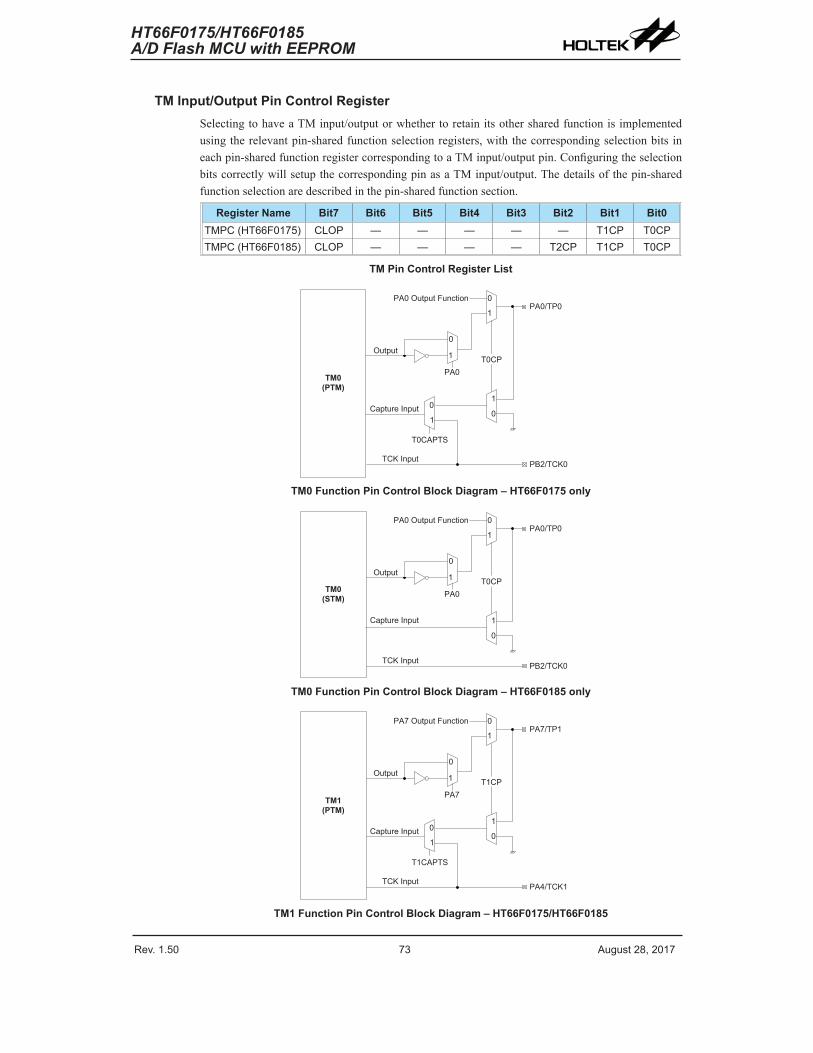
Rev. 1.50 �� ����st ��� �01� Rev. 1.50 �3 ����st ��� �01�
HT66F0175/HT66F0185A/D Flash MCU with EEPROM
HT66F0175/HT66F0185A/D Flash MCU with EEPROM
TM Input/Output Pin Control RegisterSelectingtohaveaTMinput/outputorwhethertoretainitsothersharedfunctionisimplementedusingtherelevantpin-sharedfunctionselectionregisters,withthecorrespondingselectionbits ineachpin-sharedfunctionregistercorrespondingtoaTMinput/outputpin.ConfiguringtheselectionbitscorrectlywillsetupthecorrespondingpinasaTMinput/output.Thedetailsofthepin-sharedfunctionselectionaredescribedinthepin-sharedfunctionsection.
Register Name Bit7 Bit6 Bit5 Bit4 Bit3 Bit2 Bit1 Bit0TMPC (HT66F01�5) CLOP — — — — — T1CP T0CPTMPC (HT66F01�5) CLOP — — — — T�CP T1CP T0CP
TM Pin Control Register List
TM0(PTM)
P�0/TP0
T0CP
P�0 O�tp�t F�nction 0
1
O�tp�t
Capt�re Inp�t
T0C�PTS
PB�/TCK0TCK Inp�t
0
1
P�0
0
1
1
0
TM0 Function Pin Control Block Diagram – HT66F0175 only
TM0(STM)
P�0/TP0
T0CP
P�0 O�tp�t F�nction 0
1
O�tp�t
Capt�re Inp�t
PB�/TCK0TCK Inp�t
0
1
P�0
1
0
TM0 Function Pin Control Block Diagram – HT66F0185 only
TM1(PTM)
P��/TP1
T1CP
P�� O�tp�t F�nction 0
1
O�tp�t
Capt�re Inp�t
T1C�PTS
P�4/TCK1TCK Inp�t
0
1
P��
0
1
1
0
TM1 Function Pin Control Block Diagram – HT66F0175/HT66F0185
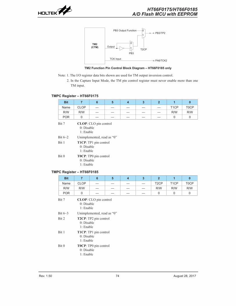
Rev. 1.50 �4 ����st ��� �01� Rev. 1.50 �5 ����st ��� �01�
HT66F0175/HT66F0185A/D Flash MCU with EEPROM
HT66F0175/HT66F0185A/D Flash MCU with EEPROM
TM2(CTM)
PB3/TP�
T�CP
PB3 O�tp�t F�nction 0
1
O�tp�t
P�6/TCK�TCK Inp�t
0
1
PB3
TM2 Function Pin Control Block Diagram – HT66F0185 only
Note:1.TheI/OregisterdatabitsshownareusedforTMoutputinversioncontrol.2.IntheCaptureInputMode,theTMpincontrolregistermustneverenablemorethanoneTMinput.
TMPC Register – HT66F0175
Bit 7 6 5 4 3 2 1 0Name CLOP — — — — — T1CP T0CPR/W R/W — — — — — R/W R/WPOR 0 — — — — — 0 0
Bit7 CLOP:CLOpincontrol0:Disable1:Enable
Bit6~2 Unimplemented,readas“0”Bit1 T1CP:TP1pincontrol
0:Disable1:Enable
Bit0 T0CP:TP0pincontrol0:Disable1:Enable
TMPC Register – HT66F0185
Bit 7 6 5 4 3 2 1 0Name CLOP — — — — T�CP T1CP T0CPR/W R/W — — — — R/W R/W R/WPOR 0 — — — — 0 0 0
Bit7 CLOP:CLOpincontrol0:Disable1:Enable
Bit6~3 Unimplemented,readas“0”Bit2 T2CP:TP2pincontrol
0:Disable1:Enable
Bit1 T1CP:TP1pincontrol0:Disable1:Enable
Bit0 T0CP:TP0pincontrol0:Disable1:Enable

Rev. 1.50 �4 ����st ��� �01� Rev. 1.50 �5 ����st ��� �01�
HT66F0175/HT66F0185A/D Flash MCU with EEPROM
HT66F0175/HT66F0185A/D Flash MCU with EEPROM
Programming ConsiderationsTheTMCounterRegistersandtheCapture/CompareCCRAandCCRPregisters,beingeither10-bitor16-bit,allhavealowandhighbytestructure.Thehighbytescanbedirectlyaccessed,butasthelowbytescanonlybeaccessedviaaninternal8-bitbuffer,readingorwritingtotheseregisterpairsmustbecarriedoutinaspecificway.Theimportantpointtonoteisthatdatatransfertoandfromthe8-bitbufferanditsrelatedlowbyteonlytakesplacewhenawriteorreadoperationtoitscorrespondinghighbyteisexecuted.
AstheCCRAandCCRPregistersareimplementedinthewayshowninthefollowingdiagramandaccessingtheseregisterpairsiscarriedoutinaspecificwayasdescribedabove,itisrecommendedtousethe“MOV”instructiontoaccesstheCCRAandCCRPlowbyteregisters,namedTMnALandTMnRPL,usingthefollowingaccessprocedures.AccessingtheCCRAorCCRPlowbyteregisterswithoutfollowingtheseaccessprocedureswillresultinunpredictablevalues.
Data B�s
�-bit B�ffer
TMnDHTMnDL
TMn�HTMn�L
TMn Co�nter Re�ister (Read only)
TMn CCR� Re�ister (Read/Write)
TMnRPHTMnRPL
PTM CCRP Re�ister (Read/Write)
Thefollowingstepsshowthereadandwriteprocedures:
• WritingDatatoCCRAorCCRP♦ Step1.WritedatatoLowByteTMnALorTMnRPL
– notethatheredataisonlywrittentothe8-bitbuffer.♦ Step2.WritedatatoHighByteTMnAHorTMnRPH
– heredata iswrittendirectly to thehighbyteregistersandsimultaneouslydata is latchedfromthe8-bitbuffertotheLowByteregisters.
• ReadingDatafromtheCounterRegistersandCCRAorCCRP♦ Step1.ReaddatafromtheHighByteTMnDH,TMnAHorTMnRPH
– heredataisreaddirectlyfromtheHighByteregistersandsimultaneouslydataislatchedfromtheLowByteregisterintothe8-bitbuffer.
♦ Step2.ReaddatafromtheLowByteTMnDL,TMnALorTMnRPL– thisstepreadsdatafromthe8-bitbuffer.
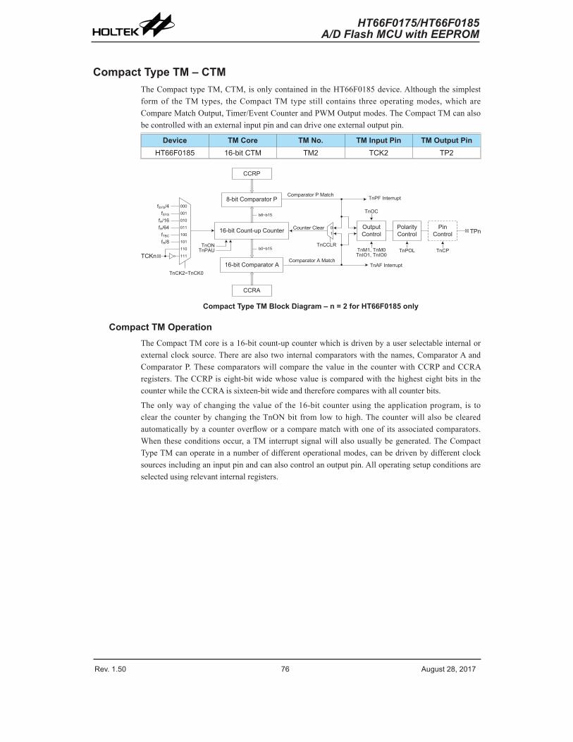
Rev. 1.50 �6 ����st ��� �01� Rev. 1.50 �� ����st ��� �01�
HT66F0175/HT66F0185A/D Flash MCU with EEPROM
HT66F0175/HT66F0185A/D Flash MCU with EEPROM
Compact Type TM – CTMTheCompacttypeTM,CTM,isonlycontainedintheHT66F0185device.Althoughthesimplestformof theTMtypes, theCompactTMtypestill contains threeoperatingmodes,whichareCompareMatchOutput,Timer/EventCounterandPWMOutputmodes.TheCompactTMcanalsobecontrolledwithanexternalinputpinandcandriveoneexternaloutputpin.
Device TM Core TM No. TM Input Pin TM Output PinHT66F01�5 16-bit CTM TM� TCK� TP�
fSYS
fSYS/4
fH/64fH/16
fTBC
TCKn
000
001
010
011
100
101
110
111
TnCK�~TnCK0
16-bit Co�nt-�p Co�nter
�-bit Comparator P
CCRP
b�~b15
b0~b15
16-bit Comparator �
TnONTnP�U
Comparator � Match
Comparator P Match
Co�nter Clear 01
O�tp�t Control
Polarity Control
Pin Control TPn
TnOC
TnM1� TnM0TnIO1� TnIO0
Tn�F Interr�pt
TnPF Interr�pt
TnPOL TnCP
CCR�
TnCCLRfH/�
Compact Type TM Block Diagram – n = 2 for HT66F0185 only
Compact TM OperationTheCompactTMcoreisa16-bitcount-upcounterwhichisdrivenbyauserselectableinternalorexternalclocksource.Therearealsotwointernalcomparatorswiththenames,ComparatorAandComparatorP.Thesecomparatorswillcompare thevalue in thecounterwithCCRPandCCRAregisters.TheCCRPiseight-bitwidewhosevalueiscomparedwiththehighesteightbits inthecounterwhiletheCCRAissixteen-bitwideandthereforecompareswithallcounterbits.
Theonlywayofchanging thevalueof the16-bitcounterusing theapplicationprogram, is toclear thecounterbychanging theTnONbit fromlowtohigh.Thecounterwillalsobeclearedautomaticallybyacounteroverfloworacomparematchwithoneof itsassociatedcomparators.Whentheseconditionsoccur,aTMinterruptsignalwillalsousuallybegenerated.TheCompactTypeTMcanoperateinanumberofdifferentoperationalmodes,canbedrivenbydifferentclocksourcesincludinganinputpinandcanalsocontrolanoutputpin.Alloperatingsetupconditionsareselectedusingrelevantinternalregisters.

Rev. 1.50 �6 ����st ��� �01� Rev. 1.50 �� ����st ��� �01�
HT66F0175/HT66F0185A/D Flash MCU with EEPROM
HT66F0175/HT66F0185A/D Flash MCU with EEPROM
Compact Type TM Register DescriptionOveralloperationoftheCompactTMiscontrolledusingaseriesofregisters.Areadonlyregisterpairexiststostoretheinternalcounter16-bitvalue,whilearead/writeregisterpairexiststostoretheinternal16-bitCCRAvalue.Thereisalsoaread/writeregisterusedtostoretheinternal8-bitCCRPvalue.Theremainingtworegistersarecontrolregisterswhichsetupthedifferentoperatingandcontrolmodes.
Register Name Bit7 Bit6 Bit5 Bit4 Bit3 Bit2 Bit1 Bit0
TMnC0 TnP�U TnCK� TnCK1 TnCK0 TnON — — —TMnC1 TnM1 TnM0 TnIO1 TnIO0 TnOC TnPOL TnDPX TnCCLRTMnDL D� D6 D5 D4 D3 D� D1 D0TMnDH D15 D14 D13 D1� D11 D10 D9 D�TMn�L D� D6 D5 D4 D3 D� D1 D0TMn�H D15 D14 D13 D1� D11 D10 D9 D�TMnRP TnRP� TnRP6 TnRP5 TnRP4 TnRP3 TnRP� TnRP1 TnRP0
16-bit Compact TM Registers List – n = 2 for for HT66F0185 only
TMnDL Register
Bit 7 6 5 4 3 2 1 0Name D� D6 D5 D4 D3 D� D1 D0R/W R R R R R R R RPOR 0 0 0 0 0 0 0 0
Bit7~0 TMnCounterLowByteRegisterbit7~bit0TMn16-bitCounterbit7~bit0
TMnDH Register
Bit 7 6 5 4 3 2 1 0Name D15 D14 D13 D1� D11 D10 D9 D�R/W R R R R R R R RPOR 0 0 0 0 0 0 0 0
Bit7~0 TMnCounterHighByteRegisterbit7~bit0TMn16-bitCounterbit15~bit8
TMnAL Register
Bit 7 6 5 4 3 2 1 0Name D� D6 D5 D4 D3 D� D1 D0R/W R/W R/W R/W R/W R/W R/W R/W R/WPOR 0 0 0 0 0 0 0 0
Bit7~0 TMnCCRALowByteRegisterbit7~bit0TMn16-bitCCRAbit7~bit0
TMnAH Register
Bit 7 6 5 4 3 2 1 0Name D15 D14 D13 D1� D11 D10 D9 D�R/W R/W R/W R/W R/W R/W R/W R/W R/WPOR 0 0 0 0 0 0 0 0
Bit7~0 TMnCCRAHighByteRegisterbit7~bit0TMn16-bitCCRAbit15~bit8
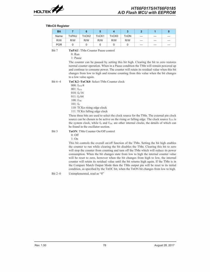
Rev. 1.50 �� ����st ��� �01� Rev. 1.50 �9 ����st ��� �01�
HT66F0175/HT66F0185A/D Flash MCU with EEPROM
HT66F0175/HT66F0185A/D Flash MCU with EEPROM
TMnC0 Register
Bit 7 6 5 4 3 2 1 0Name TnP�U TnCK� TnCK1 TnCK0 TnON — — —R/W R/W R/W R/W R/W R/W — — —POR 0 0 0 0 0 — — —
Bit7 TnPAU:TMnCounterPausecontrol0:Run1:Pause
Thecountercanbepausedbysettingthisbithigh.Clearingthebit tozerorestoresnormalcounteroperation.WheninaPauseconditiontheTMnwillremainpoweredupandcontinuetoconsumepower.Thecounterwillretainitsresidualvaluewhenthisbitchangesfromlowtohighandresumecountingfromthisvaluewhenthebitchangestoalowvalueagain.
Bit6~4 TnCK2~TnCK0:SelectTMnCounterclock000:fSYS/4001:fSYS
010:fH/16011:fH/64100:fTBC101:fH110:TCKnrisingedgeclock111:TCKnfallingedgeclock
ThesethreebitsareusedtoselecttheclocksourcefortheTMn.Theexternalpinclocksourcecanbechosentobeactiveontherisingorfallingedge.TheclocksourcefSYSisthesystemclock,whilefHandfTBCareotherinternalclocks,thedetailsofwhichcanbefoundintheoscillatorsection.
Bit3 TnON:TMnCounterOn/Offcontrol0:Off1:On
Thisbitcontrolstheoverallon/offfunctionoftheTMn.SettingthebithighenablesthecountertorunwhileclearingthebitdisablestheTMn.Clearingthisbit tozerowillstopthecounterfromcountingandturnofftheTMnwhichwillreduceitspowerconsumption.Whenthebitchangesstatefromlowtohightheinternalcountervaluewillbereset tozero,howeverwhenthebitchangesfromhighto low, the internalcounterwillretainitsresidualvalueuntilthebitreturnshighagain.IftheTMnisintheCompareMatchOutputModethentheTMnoutputpinwillberesettoitsinitialcondition,asspecifiedbytheTnOCbit,whentheTnONbitchangesfromlowtohigh.
Bit2~0 Unimplemented,readas“0”

Rev. 1.50 �� ����st ��� �01� Rev. 1.50 �9 ����st ��� �01�
HT66F0175/HT66F0185A/D Flash MCU with EEPROM
HT66F0175/HT66F0185A/D Flash MCU with EEPROM
TMnC1 Register
Bit 7 6 5 4 3 2 1 0Name TnM1 TnM0 TnIO1 TnIO0 TnOC TnPOL TnDPX TnCCLRR/W R/W R/W R/W R/W R/W R/W R/W R/WPOR 0 0 0 0 0 0 0 0
Bit7~6 TnM1~TnM0:SelectTMnOperatingMode00:CompareMatchOutputMode01:Undefined10:PWMMode11:Timer/CounterMode
ThesebitssetuptherequiredoperatingmodefortheTMn.ToensurereliableoperationtheTMnshouldbeswitchedoffbeforeanychangesaremadetotheTnM1andTnM0bits.IntheTimer/CounterMode,theTMnoutputpincontrolwillbedisabled.
Bit5~4 TnIO1~TnIO0:SelectTPnpinoutputfunctionCompareMatchOutputMode00:Nochange01:Outputlow10:Outputhigh11:Toggleoutput
PWMOutputMode00:PWMoutputinactivestate01:PWMoutputactivestate10:PWMoutput11:Undefined
Timer/CounterModeUnused
ThesetwobitsareusedtodeterminehowtheTMnoutputpinchangesstatewhenacertainconditionisreached.ThefunctionthatthesebitsselectdependsuponinwhichmodetheTMnisrunning.IntheCompareMatchOutputMode,theTnIO1andTnIO0bitsdeterminehowtheTMnoutputpinchangesstatewhenacomparematchoccursfromtheComparatorA.TheTMnoutputpincanbesetuptoswitchhigh,switchlowortotoggleitspresentstatewhenacomparematchoccursfromtheComparatorA.Whenthebitsarebothzero,thennochangewilltakeplaceontheoutput.TheinitialvalueoftheTMnoutputpinshouldbesetupusingtheTnOCbit intheTMnC1register.NotethattheoutputlevelrequestedbytheTnIO1andTnIO0bitsmustbedifferentfromtheinitialvaluesetupusingtheTnOCbitotherwisenochangewilloccurontheTMnoutputpinwhenacomparematchoccurs.AftertheTMnoutputpinchangesstate,itcanberesettoitsinitiallevelbychangingtheleveloftheTnONbitfromlowtohigh.In thePWMMode, theTnIO1andTnIO0bitsdeterminehowtheTMnoutputpinchangesstatewhenacertaincomparematchconditionoccurs.ThePWMoutputfunctionismodifiedbychangingthesetwobits. It isnecessarytoonlychangethevaluesof theTnIO1andTnIO0bitsonlyafter theTMnhasbeen switchedoff.UnpredictablePWMoutputswilloccuriftheTnIO1andTnIO0bitsarechangedwhentheTMnisrunning.
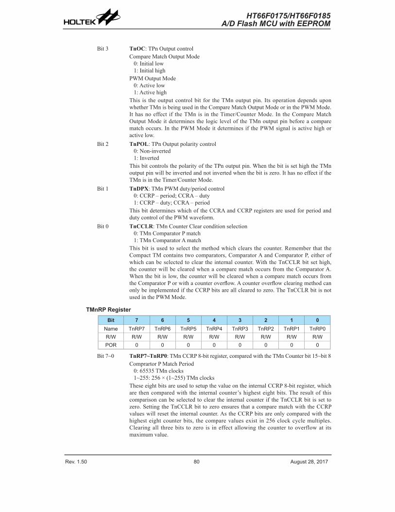
Rev. 1.50 �0 ����st ��� �01� Rev. 1.50 �1 ����st ��� �01�
HT66F0175/HT66F0185A/D Flash MCU with EEPROM
HT66F0175/HT66F0185A/D Flash MCU with EEPROM
Bit3 TnOC:TPnOutputcontrolCompareMatchOutputMode0:Initiallow1:Initialhigh
PWMOutputMode0:Activelow1:Activehigh
This is theoutputcontrolbit for theTMnoutputpin. ItsoperationdependsuponwhetherTMnisbeingusedintheCompareMatchOutputModeorinthePWMMode.Ithasnoeffect if theTMnis in theTimer/CounterMode. In theCompareMatchOutputModeitdeterminesthelogiclevelof theTMnoutputpinbeforeacomparematchoccurs.InthePWMModeitdeterminesif thePWMsignal isactivehighoractivelow.
Bit2 TnPOL:TPnOutputpolaritycontrol0:Non-inverted1:Inverted
ThisbitcontrolsthepolarityoftheTPnoutputpin.WhenthebitissethightheTMnoutputpinwillbeinvertedandnotinvertedwhenthebitiszero.IthasnoeffectiftheTMnisintheTimer/CounterMode.
Bit1 TnDPX:TMnPWMduty/periodcontrol0:CCRP–period;CCRA–duty1:CCRP–duty;CCRA–period
ThisbitdetermineswhichoftheCCRAandCCRPregistersareusedforperiodanddutycontrolofthePWMwaveform.
Bit0 TnCCLR:TMnCounterClearconditionselection0:TMnComparatorPmatch1:TMnComparatorAmatch
Thisbit isused toselect themethodwhichclears thecounter.Remember that theCompactTMcontainstwocomparators,ComparatorAandComparatorP,eitherofwhichcanbeselectedtoclear the internalcounter.With theTnCCLRbitsethigh,thecounterwillbeclearedwhenacomparematchoccursfromtheComparatorA.Whenthebitislow,thecounterwillbeclearedwhenacomparematchoccursfromtheComparatorPorwithacounteroverflow.AcounteroverflowclearingmethodcanonlybeimplementediftheCCRPbitsareallclearedtozero.TheTnCCLRbitisnotusedinthePWMMode.
TMnRP Register
Bit 7 6 5 4 3 2 1 0Name TnRP� TnRP6 TnRP5 TnRP4 TnRP3 TnRP� TnRP1 TnRP0R/W R/W R/W R/W R/W R/W R/W R/W R/WPOR 0 0 0 0 0 0 0 0
Bit7~0 TnRP7~TnRP0:TMnCCRP8-bitregister,comparedwiththeTMnCounterbit15~bit8ComprartorPMatchPeriod0:65535TMnclocks1~255:256×(1~255)TMnclocks
TheseeightbitsareusedtosetupthevalueontheinternalCCRP8-bitregister,whichare thencomparedwith the internalcounter’shighesteightbits.Theresultof thiscomparisoncanbeselectedtoclear theinternalcounterif theTnCCLRbit isset tozero.SettingtheTnCCLRbit tozeroensuresthatacomparematchwiththeCCRPvalueswillreset theinternalcounter.AstheCCRPbitsareonlycomparedwiththehighesteightcounterbits, thecomparevaluesexist in256clockcyclemultiples.Clearingall threebits tozero is ineffectallowing thecounter tooverflowat itsmaximumvalue.
Rev. 1.50 �0 ����st ��� �01� Rev. 1.50 �1 ����st ��� �01�
HT66F0175/HT66F0185A/D Flash MCU with EEPROM
HT66F0175/HT66F0185A/D Flash MCU with EEPROM
Compact Type TM Operation ModesTheCompactTypeTMcanoperateinoneofthreeoperatingmodes,CompareMatchOutputMode,PWMModeorTimer/CounterMode.TheoperatingmodeisselectedusingtheTnM1andTnM0bitsintheTMnC1register.
Compare Match Output ModeToselectthismode,bitsTnM1andTnM0intheTMnC1register,shouldbesetto“00”respectively.Inthismodeoncethecounterisenabledandrunningitcanbeclearedbythreemethods.Theseareacounteroverflow,acomparematchfromComparatorAandacomparematchfromComparatorP.WhentheTnCCLRbitislow,therearetwowaysinwhichthecountercanbecleared.OneiswhenacomparematchoccursfromComparatorP, theotheriswhentheCCRPbitsareallzerowhichallowsthecountertooverflow.HerebothTnAFandTnPFinterruptrequestflagsfortheComparatorAandComparatorPrespectively,willbothbegenerated.
IftheTnCCLRbitintheTMnC1registerishighthenthecounterwillbeclearedwhenacomparematchoccurs fromComparatorA.However,hereonly theTnAFinterrupt request flagwillbegeneratedevenifthevalueoftheCCRPbitsislessthanthatoftheCCRAregisters.ThereforewhenTnCCLRishighnoTMnPFinterruptrequestflagwillbegenerated.IftheCCRAbitsareallzero,thecounterwilloverflowwhenitsreachesitsmaximum1-bit,FFFFHex,value,howeverheretheTnAFinterruptrequestflagwillnotbegenerated.
Asthenameof themodesuggests,afteracomparisonismade, theTMnoutputpinwillchangestate.TheTMnoutputpinconditionhoweveronlychangesstatewhenaTnAFinterruptrequestflagisgeneratedafteracomparematchoccursfromComparatorA.TheTnPFinterruptrequestflag,generatedfromacomparematchoccursfromComparatorP,willhavenoeffectontheTMnoutputpin.ThewayinwhichtheTMnoutputpinchangesstatearedeterminedbytheconditionof theTnIO1andTnIO0bitsintheTMnC1register.TheTMnoutputpincanbeselectedusingtheTnIO1andTnIO0bitstogohigh,togolowortotogglefromitspresentconditionwhenacomparematchoccursfromComparatorA.Theinitialconditionof theTMnoutputpin,whichissetupafter theTnONbitchangesfromlowtohigh,issetupusingtheTnOCbit.NotethatiftheTnIO1andTnIO0bitsarezerothennopinchangewilltakeplace.

Rev. 1.50 �� ����st ��� �01� Rev. 1.50 �3 ����st ��� �01�
HT66F0175/HT66F0185A/D Flash MCU with EEPROM
HT66F0175/HT66F0185A/D Flash MCU with EEPROM
Co�nter Val�e
0xFFFF
CCRP
CCR�
TnON
TnP�U
TnPOL
CCRP Int. fla� TnPF
CCR� Int. fla� Tn�F
TMn O/P Pin
Time
CCRP=0
CCRP > 0
Co�nter overflowCCRP > 0Co�nter cleared by CCRP val�e
Pa�se
Res�me
Stop
Co�nter Restart
TnCCLR = 0; TnM [1:0] = 00
O�tp�t pin set to initial Level Low if TnOC=0
O�tp�t To��le with Tn�F fla�
Note TnIO [1:0] = 10 �ctive Hi�h O�tp�t selectHere TnIO [1:0] = 11
To��le O�tp�t select
O�tp�t not affected by Tn�F fla�. Remains Hi�h �ntil reset by TnON bit
O�tp�t PinReset to Initial val�e
O�tp�t controlled by other pin-shared f�nction
O�tp�t Invertswhen TnPOL is hi�h
Compare Match Output Mode – TnCCLR = 0Note:1.WithTnCCLR=0,aComparatorPmatchwillclearthecounter
2.TheTMnoutputpincontrolledonlybyTnAFflag3.TheoutputpinisresettoitsinitialstatebyTnONbitrisingedge4.n=2forHT66F0185only
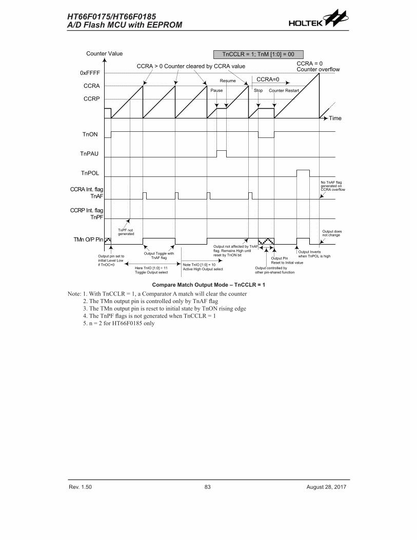
Rev. 1.50 �� ����st ��� �01� Rev. 1.50 �3 ����st ��� �01�
HT66F0175/HT66F0185A/D Flash MCU with EEPROM
HT66F0175/HT66F0185A/D Flash MCU with EEPROM
Co�nter Val�e
0xFFFF
CCRP
CCR�
TnON
TnP�U
TnPOL
TMn O/P Pin
Time
CCR�=0
CCR� = 0Co�nter overflowCCR� > 0 Co�nter cleared by CCR� val�e
Pa�se
Res�me
Stop Co�nter Restart
TnCCLR = 1; TnM [1:0] = 00
O�tp�t pin set to initial Level Low if TnOC=0
O�tp�t To��le with Tn�F fla�
Note TnIO [1:0] = 10 �ctive Hi�h O�tp�t selectHere TnIO [1:0] = 11
To��le O�tp�t select
O�tp�t not affected by Tn�F fla�. Remains Hi�h �ntil reset by TnON bit
O�tp�t PinReset to Initial val�e
O�tp�t controlled by other pin-shared f�nction
O�tp�t Invertswhen TnPOL is hi�h
TnPF not �enerated
No Tn�F fla� �enerated on CCR� overflow
O�tp�t does not chan�e
CCR� Int. fla� Tn�F
CCRP Int. fla� TnPF
Compare Match Output Mode – TnCCLR = 1Note:1.WithTnCCLR=1,aComparatorAmatchwillclearthecounter
2.TheTMnoutputpiniscontrolledonlybyTnAFflag3.TheTMnoutputpinisresettoinitialstatebyTnONrisingedge4.TheTnPFflagsisnotgeneratedwhenTnCCLR=15.n=2forHT66F0185only
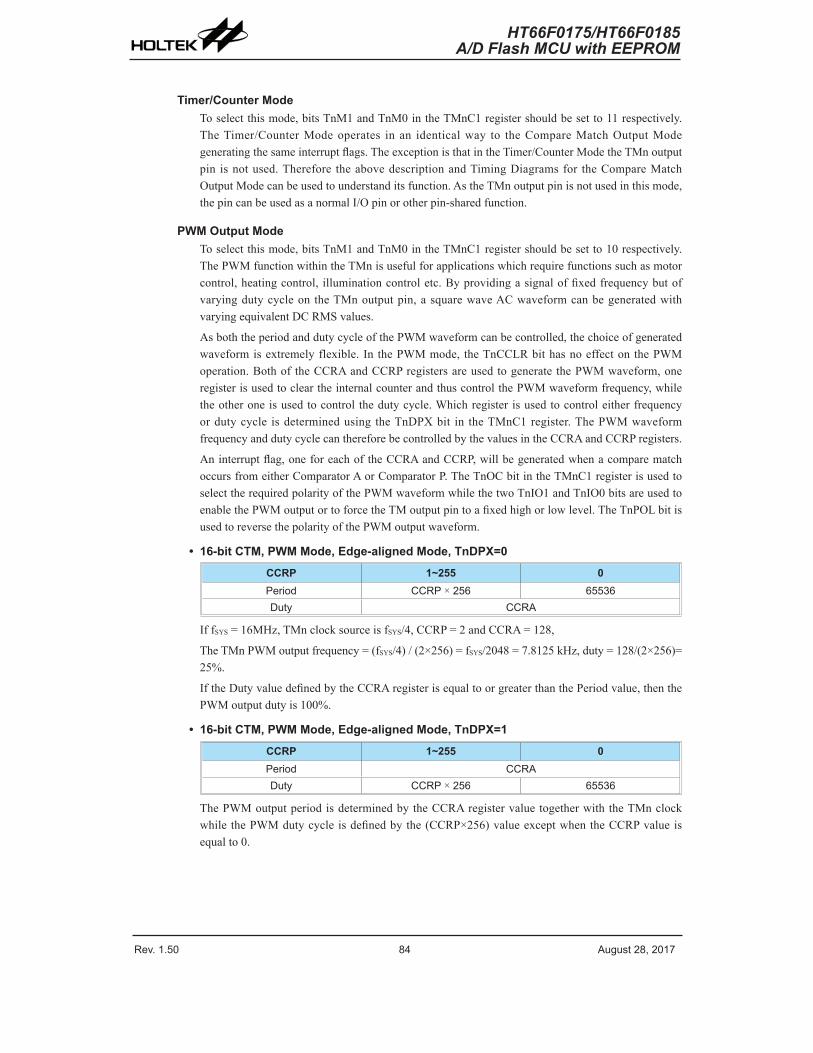
Rev. 1.50 �4 ����st ��� �01� Rev. 1.50 �5 ����st ��� �01�
HT66F0175/HT66F0185A/D Flash MCU with EEPROM
HT66F0175/HT66F0185A/D Flash MCU with EEPROM
Timer/Counter ModeToselectthismode,bitsTnM1andTnM0intheTMnC1registershouldbesetto11respectively.TheTimer/CounterModeoperates in an identicalway to theCompareMatchOutputModegeneratingthesameinterruptflags.TheexceptionisthatintheTimer/CounterModetheTMnoutputpin isnotused.Therefore theabovedescriptionandTimingDiagramsfor theCompareMatchOutputModecanbeusedtounderstanditsfunction.AstheTMnoutputpinisnotusedinthismode,thepincanbeusedasanormalI/Opinorotherpin-sharedfunction.
PWM Output ModeToselectthismode,bitsTnM1andTnM0intheTMnC1registershouldbesetto10respectively.ThePWMfunctionwithintheTMnisusefulforapplicationswhichrequirefunctionssuchasmotorcontrol,heatingcontrol, illuminationcontroletc.Byprovidingasignaloffixedfrequencybutofvaryingdutycycleon theTMnoutputpin,asquarewaveACwaveformcanbegeneratedwithvaryingequivalentDCRMSvalues.
AsboththeperiodanddutycycleofthePWMwaveformcanbecontrolled,thechoiceofgeneratedwaveformisextremelyflexible.In thePWMmode, theTnCCLRbithasnoeffectonthePWMoperation.Bothof theCCRAandCCRPregistersareusedtogeneratethePWMwaveform,oneregisterisusedtocleartheinternalcounterandthuscontrolthePWMwaveformfrequency,whiletheotheroneisusedtocontrol thedutycycle.Whichregister isusedtocontroleitherfrequencyordutycycle isdeterminedusing theTnDPXbit in theTMnC1register.ThePWMwaveformfrequencyanddutycyclecanthereforebecontrolledbythevaluesintheCCRAandCCRPregisters.
Aninterruptflag,oneforeachoftheCCRAandCCRP,willbegeneratedwhenacomparematchoccursfromeitherComparatorAorComparatorP.TheTnOCbitintheTMnC1registerisusedtoselecttherequiredpolarityofthePWMwaveformwhilethetwoTnIO1andTnIO0bitsareusedtoenablethePWMoutputortoforcetheTMoutputpintoafixedhighorlowlevel.TheTnPOLbitisusedtoreversethepolarityofthePWMoutputwaveform.
• 16-bit CTM, PWM Mode, Edge-aligned Mode, TnDPX=0
CCRP 1~255 0Period CCRP × �56 65536D�ty CCR�
IffSYS=16MHz,TMnclocksourceisfSYS/4,CCRP=2andCCRA=128,
TheTMnPWMoutputfrequency=(fSYS/4)/(2×256)=fSYS/2048=7.8125kHz,duty=128/(2×256)=25%.
IftheDutyvaluedefinedbytheCCRAregisterisequaltoorgreaterthanthePeriodvalue,thenthePWMoutputdutyis100%.
• 16-bit CTM, PWM Mode, Edge-aligned Mode, TnDPX=1
CCRP 1~255 0Period CCR�D�ty CCRP × �56 65536
ThePWMoutputperiodisdeterminedbytheCCRAregistervaluetogetherwiththeTMnclockwhilethePWMdutycycleisdefinedbythe(CCRP×256)valueexceptwhentheCCRPvalueisequalto0.
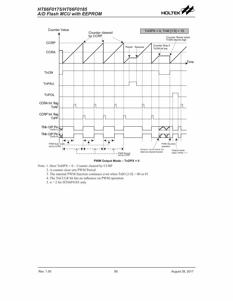
Rev. 1.50 �4 ����st ��� �01� Rev. 1.50 �5 ����st ��� �01�
HT66F0175/HT66F0185A/D Flash MCU with EEPROM
HT66F0175/HT66F0185A/D Flash MCU with EEPROM
Co�nter Val�e
CCRP
CCR�
TnON
TnP�U
TnPOL
TMn O/P Pin (TnOC=1)
Time
Co�nter cleared by CCRP
Pa�se Res�me Co�nter Stop if TnON bit low
Co�nter Reset when TnON ret�rns hi�h
TnDPX = 0; TnM [1:0] = 10
PWM D�ty Cycle set by CCR�
PWM res�mes operation
O�tp� t con t ro l led by other pin-shared f�nction
O�tp�t Invertswhen TnPOL = 1PWM Period
set by CCRP
TMn O/P Pin (TnOC=0)
CCR� Int. fla� Tn�F
CCRP Int. fla� TnPF
PWM Output Mode – TnDPX = 0Note:1.HereTnDPX=0–CounterclearedbyCCRP
2.AcounterclearsetsPWMPeriod3.TheinternalPWMfunctioncontinuesevenwhenTnIO[1:0]=00or014.TheTnCCLRbithasnoinfluenceonPWMoperation5.n=2forHT66F0185only

Rev. 1.50 �6 ����st ��� �01� Rev. 1.50 �� ����st ��� �01�
HT66F0175/HT66F0185A/D Flash MCU with EEPROM
HT66F0175/HT66F0185A/D Flash MCU with EEPROM
Co�nter Val�e
CCRP
CCR�
TnON
TnP�U
TnPOL
CCRP Int. fla� TnPF
CCR� Int. fla� Tn�F
TMn O/P Pin (TnOC=1)
Time
Co�nter cleared by CCR�
Pa�se Res�me Co�nter Stop if TnON bit low
Co�nter Reset when TnON ret�rns hi�h
TnDPX = 1; TnM [1:0] = 10
PWM D�ty Cycle set by CCRP
PWM res�mes operation
O�tp�t controlled by other pin-shared f�nction O�tp�t Inverts
when TnPOL = 1PWM Period set by CCR�
TMn O/P Pin (TnOC=0)
PWM Output Mode – TnDPX = 1Note:1.HereTnDPX=1–CounterclearedbyCCRA
2.AcounterclearsetsPWMPeriod3.TheinternalPWMfunctioncontinuesevenwhenTnIO[1:0]=00or014.TheTnCCLRbithasnoinfluenceonPWMoperation5.n=2forHT66F0185only

Rev. 1.50 �6 ����st ��� �01� Rev. 1.50 �� ����st ��� �01�
HT66F0175/HT66F0185A/D Flash MCU with EEPROM
HT66F0175/HT66F0185A/D Flash MCU with EEPROM
Standard Type TM – STMTheStandardTypeTM,STM,isonlycontainedintheHT66F0185device.TheStandardTypeTMcontainsfiveoperatingmodes,whichareCompareMatchOutput,Timer/EventCounter,CaptureInput,SinglePulseOutputandPWMOutputmodes.TheStandardTMcanalsobecontrolledwithanexternalinputpinandcandriveoneexternaloutputpin.
Device TM Core TM No. TM Input Pin TM Output PinHT66F01�5 16-bit STM TM0 TCK0 TP0
fSYS
fSYS/4
fH/64fH/16
fTBC
TCKn
000
001
010
011
100
101
110
111
TnCK�~TnCK0
16-bit Co�nt-�p Co�nter
�-bit Comparator P
CCRP
b�~b15
b0~b15
16-bit Comparator �
TnONTnP�U
Comparator � Match
Comparator P Match
Co�nter Clear 01
O�tp�t Control
Polarity Control
Pin Control TPn
TnOC
TnM1� TnM0TnIO1� TnIO0
Tn�F Interr�pt
TnPF Interr�pt
TnPOL TnCP
CCR�
TnCCLR
Ed�eDetector
TnIO1� TnIO0
fH/�
Standard Type TM Block Diagram – n = 0 for HT66F0185 only
Standard TM OperationThesizeofStandardTMis16-bitwideanditscoreisa16-bitcount-upcounterwhichisdrivenbyauserselectableinternalorexternalclocksource.Therearealsotwointernalcomparatorswiththenames,ComparatorAandComparatorP.ThesecomparatorswillcomparethevalueinthecounterwithCCRPandCCRAregisters.TheCCRPcomparatoris8-bitwidewhosevalueiscomparedthewithhighesteightbitsinthecounterwhiletheCCRAisthesixteenbitsandthereforecomparesallcounterbits.
Theonlywayofchanging thevalueof the16-bitcounterusing theapplicationprogram, is toclear thecounterbychanging theTnONbit fromlowtohigh.Thecounterwillalsobeclearedautomaticallybyacounteroverfloworacomparematchwithoneof itsassociatedcomparators.Whentheseconditionsoccur,aTMinterruptsignalwillalsousuallybegenerated.TheStandardTypeTMcanoperateinanumberofdifferentoperationalmodes,canbedrivenbydifferentclocksourcesincludinganinputpinandcanalsocontrolanoutputpin.Alloperatingsetupconditionsareselectedusingrelevantinternalregisters.

Rev. 1.50 �� ����st ��� �01� Rev. 1.50 �9 ����st ��� �01�
HT66F0175/HT66F0185A/D Flash MCU with EEPROM
HT66F0175/HT66F0185A/D Flash MCU with EEPROM
Standard Type TM Register DescriptionOveralloperationoftheStandardTMiscontrolledusingaseriesofregisters.Areadonlyregisterpairexiststostoretheinternalcounter16-bitvalue,whilearead/writeregisterpairexiststostoretheinternal16-bitCCRAvalue.TheTMnRPregister isusedtostorethe8-bitCCRPvalue.Theremainingtworegistersarecontrolregisterswhichsetupthedifferentoperatingandcontrolmodes.
RegisterName
Bit
7 6 5 4 3 2 1 0TMnC0 TnP�U TnCK� TnCK1 TnCK0 TnON — — —TMnC1 TnM1 TnM0 TnIO1 TnIO0 TnOC TnPOL TnDPX TnCCLRTMnDL D� D6 D5 D4 D3 D� D1 D0TMnDH D15 D14 D13 D1� D11 D10 D9 D�TMn�L D� D6 D5 D4 D3 D� D1 D0TMn�H D15 D14 D13 D1� D11 D10 D9 D�TMnRP TnRP� TnRP6 TnRP5 TnRP4 TnRP3 TnRP� TnRP1 TnRP0
16-bit Standard TM Registers List – n = 0 for HT66F0185 only
TMnDL Register
Bit 7 6 5 4 3 2 1 0Name D� D6 D5 D4 D3 D� D1 D0R/W R R R R R R R RPOR 0 0 0 0 0 0 0 0
Bit7~0 TMnCounterLowByteRegisterbit7~bit0TMn16-bitCounterbit7~bit0
TMnDH Register
Bit 7 6 5 4 3 2 1 0Name D15 D14 D13 D1� D11 D10 D9 D�R/W R R R R R R R RPOR 0 0 0 0 0 0 0 0
Bit7~0 TMnCounterHighByteRegisterbit7~bit0TMn16-bitCounterbit15~bit8
TMnAL Register
Bit 7 6 5 4 3 2 1 0Name D� D6 D5 D4 D3 D� D1 D0R/W R/W R/W R/W R/W R/W R/W R/W R/WPOR 0 0 0 0 0 0 0 0
Bit7~0 TMnCCRALowByteRegisterbit7~bit0TMn16-bitCCRAbit7~bit0
TMnAH Register
Bit 7 6 5 4 3 2 1 0Name D15 D14 D13 D1� D11 D10 D9 D�R/W R/W R/W R/W R/W R/W R/W R/W R/WPOR 0 0 0 0 0 0 0 0
Bit7~0 TMnCCRAHighByteRegisterbit7~bit0TMn16-bitCCRAbit15~bit8
Rev. 1.50 �� ����st ��� �01� Rev. 1.50 �9 ����st ��� �01�
HT66F0175/HT66F0185A/D Flash MCU with EEPROM
HT66F0175/HT66F0185A/D Flash MCU with EEPROM
TMnC0 Register
Bit 7 6 5 4 3 2 1 0Name TnP�U TnCK� TnCK1 TnCK0 TnON — — —R/W R/W R/W R/W R/W R/W — — —POR 0 0 0 0 0 — — —
Bit7 TnPAU:TMnCounterPausecontrol0:Run1:Pause
Thecountercanbepausedbysettingthisbithigh.Clearingthebit tozerorestoresnormalcounteroperation.WheninaPauseconditiontheTMnwillremainpoweredupandcontinuetoconsumepower.Thecounterwillretainitsresidualvaluewhenthisbitchangesfromlowtohighandresumecountingfromthisvaluewhenthebitchangestoalowvalueagain.
Bit6~4 TnCK2~TnCK0:SelectTMnCounterclock000:fSYS/4001:fSYS
010:fH/16011:fH/64100:fTBC101:fH110:TCKnrisingedgeclock111:TCKnfallingedgeclock
ThesethreebitsareusedtoselecttheclocksourcefortheTMn.Theexternalpinclocksourcecanbechosentobeactiveontherisingorfallingedge.TheclocksourcefSYSisthesystemclock,whilefHandfTBCareotherinternalclocks,thedetailsofwhichcanbefoundintheoscillatorsection.
Bit3 TnON:TMnCounterOn/Offcontrol0:Off1:On
Thisbitcontrolstheoverallon/offfunctionoftheTMn.SettingthebithighenablesthecountertorunwhileclearingthebitdisablestheTMn.Clearingthisbit tozerowillstopthecounterfromcountingandturnofftheTMnwhichwillreduceitspowerconsumption.Whenthebitchangesstatefromlowtohightheinternalcountervaluewillbereset tozero,howeverwhenthebitchangesfromhighto low, the internalcounterwillretainitsresidualvalueuntilthebitreturnshighagain.IftheTMnisintheCompareMatchOutputModethentheTMnoutputpinwillberesettoitsinitialcondition,asspecifiedbytheTnOCbit,whentheTnONbitchangesfromlowtohigh.
Bit2~0 Unimplemented,readas“0”
Rev. 1.50 90 ����st ��� �01� Rev. 1.50 91 ����st ��� �01�
HT66F0175/HT66F0185A/D Flash MCU with EEPROM
HT66F0175/HT66F0185A/D Flash MCU with EEPROM
TMnC1 Register
Bit 7 6 5 4 3 2 1 0Name TnM1 TnM0 TnIO1 TnIO0 TnOC TnPOL TnDPX TnCCLRR/W R/W R/W R/W R/W R/W R/W R/W R/WPOR 0 0 0 0 0 0 0 0
Bit7~6 TnM1~TnM0:SelectTMnOperatingMode00:CompareMatchOutputMode01:CaptureInputMode10:PWMModeorSinglePulseOutputMode11:Timer/CounterMode
ThesebitssetuptherequiredoperatingmodefortheTMn.ToensurereliableoperationtheTMnshouldbeswitchedoffbeforeanychangesaremadetotheTnM1andTnM0bits.IntheTimer/CounterMode,theTMnoutputpincontrolwillbedisabled.
Bit5~4 TnIO1~TnIO0:SelectTPnpinoutputfunctionCompareMatchOutputMode00:Nochange01:Outputlow10:Outputhigh11:Toggleoutput
PWMOutputMode/SinglePulseOutputMode00:PWMoutputinactivestate01:PWMoutputactivestate10:PWMoutput11:SinglePulseOutput
CaptureInputMode00:InputcaptureatrisingedgeofTPn01:InputcaptureatfallingedgeofTPn10:Inputcaptureatrising/fallingedgeofTPn11:Inputcapturedisabled
Timer/CounterModeUnused
ThesetwobitsareusedtodeterminehowtheTMnoutputpinchangesstatewhenacertainconditionisreached.ThefunctionthatthesebitsselectdependsuponinwhichmodetheTMnisrunning.IntheCompareMatchOutputMode,theTnIO1andTnIO0bitsdeterminehowtheTMnoutputpinchangesstatewhenacomparematchoccursfromtheComparatorA.TheTMoutputpincanbesetuptoswitchhigh,switchlowortotoggleitspresentstatewhenacomparematchoccursfromtheComparatorA.Whenthebitsarebothzero,thennochangewilltakeplaceontheoutput.TheinitialvalueoftheTMnoutputpinshouldbesetupusingtheTnOCbit intheTMnC1register.NotethattheoutputlevelrequestedbytheTnIO1andTnIO0bitsmustbedifferentfromtheinitialvaluesetupusingtheTnOCbitotherwisenochangewilloccurontheTMnoutputpinwhenacomparematchoccurs.AftertheTMnoutputpinchangesstate,itcanberesettoitsinitiallevelbychangingtheleveloftheTnONbitfromlowtohigh.In thePWMMode, theTnIO1andTnIO0bitsdeterminehowtheTMnoutputpinchangesstatewhenacertaincomparematchconditionoccurs.ThePWMoutputfunctionismodifiedbychangingthesetwobits. It isnecessarytoonlychangethevaluesof theTnIO1andTnIO0bitsonlyafter theTMnhasbeen switchedoff.UnpredictablePWMoutputswilloccuriftheTnIO1andTnIO0bitsarechangedwhentheTMnisrunning.
Rev. 1.50 90 ����st ��� �01� Rev. 1.50 91 ����st ��� �01�
HT66F0175/HT66F0185A/D Flash MCU with EEPROM
HT66F0175/HT66F0185A/D Flash MCU with EEPROM
Bit3 TnOC:TMnTPnOutputcontrolCompareMatchOutputMode0:Initiallow1:Initialhigh
PWMOutputMode/SinglePulseOutputMode0:Activelow1:Activehigh
This is theoutputcontrolbit for theTMnoutputpin. ItsoperationdependsuponwhetherTMnisbeingusedintheCompareMatchOutputModeorinthePWMMode/SinglePulseOutputMode.IthasnoeffectiftheTMnisintheTimer/CounterMode.IntheCompareMatchOutputModeitdeterminesthelogicleveloftheTMnoutputpinbeforeacomparematchoccurs.InthePWMMode/SinglePulseOutputModeitdeterminesifthePWMsignalisactivehighoractivelow.
Bit2 TnPOL:TMnTPnOutputpolaritycontrol0:Non-inverted1:Inverted
ThisbitcontrolsthepolarityoftheTPnoutputpin.WhenthebitissethightheTMnoutputpinwillbeinvertedandnotinvertedwhenthebitiszero.IthasnoeffectiftheTMnisintheTimer/CounterMode.
Bit1 TnDPX:TMnPWMduty/periodcontrol0:CCRP–period;CCRA–duty1:CCRP–duty;CCRA–period
ThisbitdetermineswhichoftheCCRAandCCRPregistersareusedforperiodanddutycontrolofthePWMwaveform.
Bit0 TnCCLR:TMnCounterClearconditionselection0:ComparatorPmatch1:ComparatorAmatch
Thisbit isused toselect themethodwhichclears thecounter.Remember that theStandardTMcontainstwocomparators,ComparatorAandComparatorP,eitherofwhichcanbeselectedtoclear the internalcounter.With theTnCCLRbitsethigh,thecounterwillbeclearedwhenacomparematchoccursfromtheComparatorA.Whenthebitislow,thecounterwillbeclearedwhenacomparematchoccursfromtheComparatorPorwithacounteroverflow.AcounteroverflowclearingmethodcanonlybeimplementediftheCCRPbitsareallclearedtozero.TheTnCCLRbitisnotusedinthePWMOutput,SinglePulseOutputorCaptureInputMode.

Rev. 1.50 9� ����st ��� �01� Rev. 1.50 93 ����st ��� �01�
HT66F0175/HT66F0185A/D Flash MCU with EEPROM
HT66F0175/HT66F0185A/D Flash MCU with EEPROM
TMnRP Register
Bit 7 6 5 4 3 2 1 0Name TnRP� TnRP6 TnRP5 TnRP4 TnRP3 TnRP� TnRP1 TnRP0R/W R/W R/W R/W R/W R/W R/W R/W R/WPOR 0 0 0 0 0 0 0 0
Bit7~0 TnRP7~TnRP0:TMnCCRP8-bitregister,comparedwiththeTMncounterbit15~bit8ComparatorPmatchperiod:0:65536TMnclocks1~255:(1~255)×256TMnclocks
TheseeightbitsareusedtosetupthevalueontheinternalCCRP8-bitregister,whichare thencomparedwith the internalcounter’shighesteightbits.Theresultof thiscomparisoncanbeselectedtoclear theinternalcounterif theTnCCLRbit isset tozero.SettingtheTnCCLRbit tozeroensuresthatacomparematchwiththeCCRPvalueswillreset theinternalcounter.AstheCCRPbitsareonlycomparedwiththehighesteightcounterbits, thecomparevaluesexist in256clockcyclemultiples.Clearingalleightbits tozero is ineffectallowing thecounter tooverflowat itsmaximumvalue.
Standard Type TM Operation ModesTheStandardTypeTMcanoperateinoneoffiveoperatingmodes,CompareMatchOutputMode,PWMOutputMode,SinglePulseOutputMode,CaptureInputModeorTimer/CounterMode.TheoperatingmodeisselectedusingtheTnM1andTnM0bitsintheTMnC1register.
Compare Match Output ModeToselectthismode,bitsTnM1andTnM0intheTMnC1register,shouldbesetto00respectively.Inthismodeoncethecounterisenabledandrunningitcanbeclearedbythreemethods.Theseareacounteroverflow,acomparematchfromComparatorAandacomparematchfromComparatorP.WhentheTnCCLRbitislow,therearetwowaysinwhichthecountercanbecleared.OneiswhenacomparematchfromComparatorP, theotheriswhentheCCRPbitsareallzerowhichallowsthecounter tooverflow.HerebothTnAFandTnPFinterruptrequestflagsforComparatorAandComparatorPrespectively,willbothbegenerated.
IftheTnCCLRbitintheTMnC1registerishighthenthecounterwillbeclearedwhenacomparematchoccurs fromComparatorA.However,hereonly theTnAFinterrupt request flagwillbegeneratedevenifthevalueoftheCCRPbitsislessthanthatoftheCCRAregisters.ThereforewhenTnCCLRishighnoTnPFinterruptrequestflagwillbegenerated.IntheCompareMatchOutputMode,theCCRAcannotbesetto“0”.
Asthenameofthemodesuggests,afteracomparisonismade, theTMnoutputpin,willchangestate.TheTMnoutputpinconditionhoweveronlychangesstatewhenaTnAFinterruptrequestflagisgeneratedafteracomparematchoccursfromComparatorA.TheTnPFinterruptrequestflag,generatedfromacomparematchoccursfromComparatorP,willhavenoeffectontheTMnoutputpin.ThewayinwhichtheTMnoutputpinchangesstatearedeterminedbytheconditionof theTnIO1andTnIO0bitsintheTMnC1register.TheTMnoutputpincanbeselectedusingtheTnIO1andTnIO0bitstogohigh,togolowortotogglefromitspresentconditionwhenacomparematchoccursfromComparatorA.Theinitialconditionof theTMnoutputpin,whichissetupafter theTnONbitchangesfromlowtohigh,issetupusingtheTnOCbit.NotethatiftheTnIO1andTnIO0bitsarezerothennopinchangewilltakeplace.

Rev. 1.50 9� ����st ��� �01� Rev. 1.50 93 ����st ��� �01�
HT66F0175/HT66F0185A/D Flash MCU with EEPROM
HT66F0175/HT66F0185A/D Flash MCU with EEPROM
Co�nter Val�e
0xFFFF
CCRP
CCR�
TnON
TnP�U
TnPOL
CCRP Int. fla� TnPF
CCR� Int. fla� Tn�F
TMn O/P Pin
Time
CCRP=0
CCRP > 0
Co�nter overflowCCRP > 0Co�nter cleared by CCRP val�e
Pa�se
Res�me
Stop
Co�nter Restart
TnCCLR = 0; TnM [1:0] = 00
O�tp�t pin set to initial Level Low if TnOC=0
O�tp�t To��le with Tn�F fla�
Note TnIO [1:0] = 10 �ctive Hi�h O�tp�t selectHere TnIO [1:0] = 11
To��le O�tp�t select
O�tp�t not affected by Tn�F fla�. Remains Hi�h �ntil reset by TnON bit
O�tp�t PinReset to Initial val�e
O�tp�t controlled by other pin-shared f�nction
O�tp�t Invertswhen TnPOL is hi�h
Compare Match Output Mode – TnCCLR = 0Note:1.WithTnCCLR=0aComparatorPmatchwillclearthecounter
2.TheTMnoutputpiniscontrolledonlybytheTnAFflag3.TheoutputpinisresettoitsinitialstatebyaTnONbitrisingedge4.n=0forHT66F0185only
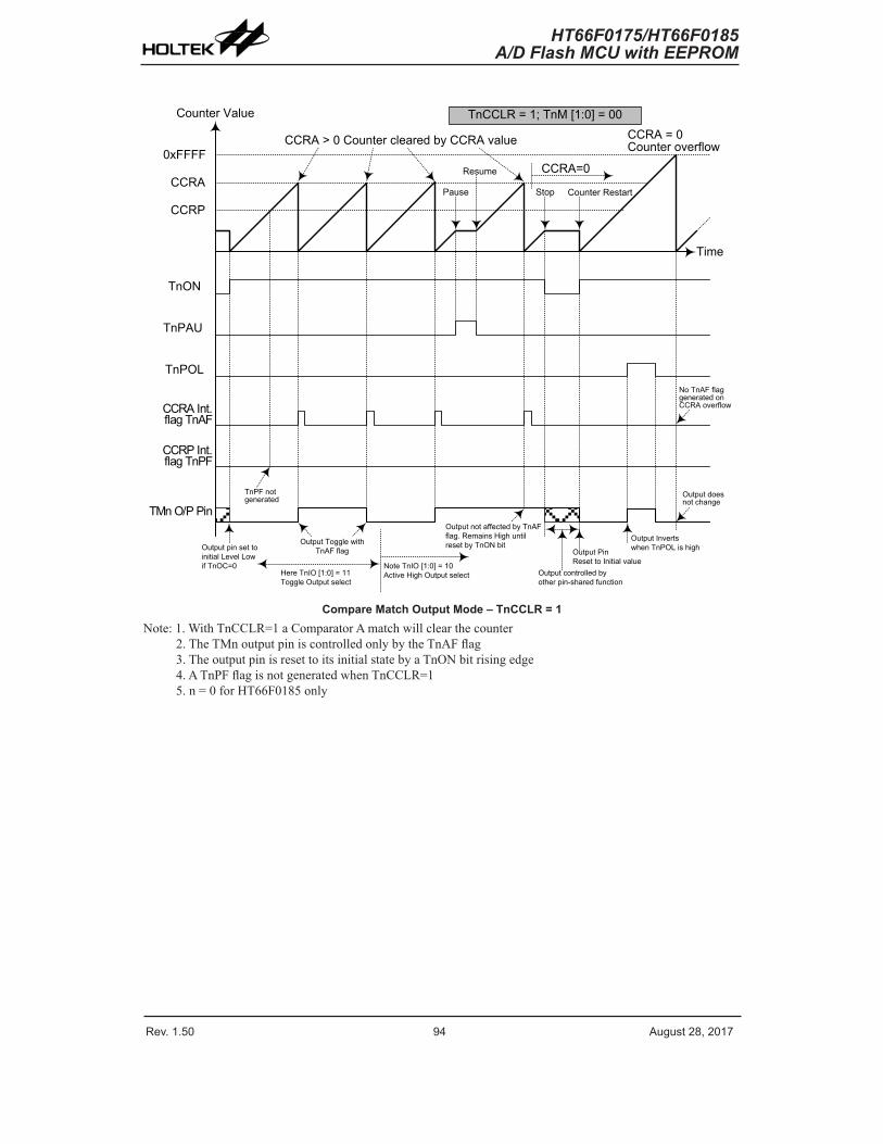
Rev. 1.50 94 ����st ��� �01� Rev. 1.50 95 ����st ��� �01�
HT66F0175/HT66F0185A/D Flash MCU with EEPROM
HT66F0175/HT66F0185A/D Flash MCU with EEPROM
Co�nter Val�e
0xFFFF
CCRP
CCR�
TnON
TnP�U
TnPOL
CCRP Int. fla� TnPF
CCR� Int. fla� Tn�F
TMn O/P Pin
Time
CCR�=0
CCR� = 0Co�nter overflowCCR� > 0 Co�nter cleared by CCR� val�e
Pa�se
Res�me
Stop Co�nter Restart
TnCCLR = 1; TnM [1:0] = 00
O�tp�t pin set to initial Level Low if TnOC=0
O�tp�t To��le with Tn�F fla�
Note TnIO [1:0] = 10 �ctive Hi�h O�tp�t selectHere TnIO [1:0] = 11
To��le O�tp�t select
O�tp�t not affected by Tn�F fla�. Remains Hi�h �ntil reset by TnON bit
O�tp�t PinReset to Initial val�e
O�tp�t controlled by other pin-shared f�nction
O�tp�t Invertswhen TnPOL is hi�h
TnPF not �enerated
No Tn�F fla� �enerated on CCR� overflow
O�tp�t does not chan�e
Compare Match Output Mode – TnCCLR = 1Note:1.WithTnCCLR=1aComparatorAmatchwillclearthecounter
2.TheTMnoutputpiniscontrolledonlybytheTnAFflag3.TheoutputpinisresettoitsinitialstatebyaTnONbitrisingedge4.ATnPFflagisnotgeneratedwhenTnCCLR=15.n=0forHT66F0185only
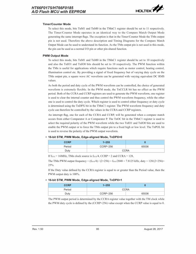
Rev. 1.50 94 ����st ��� �01� Rev. 1.50 95 ����st ��� �01�
HT66F0175/HT66F0185A/D Flash MCU with EEPROM
HT66F0175/HT66F0185A/D Flash MCU with EEPROM
Timer/Counter ModeToselectthismode,bitsTnM1andTnM0intheTMnC1registershouldbesetto11respectively.TheTimer/CounterModeoperates in an identicalway to theCompareMatchOutputModegeneratingthesameinterruptflags.TheexceptionisthatintheTimer/CounterModetheTMnoutputpin isnotused.Therefore theabovedescriptionandTimingDiagramsfor theCompareMatchOutputModecanbeusedtounderstanditsfunction.AstheTMnoutputpinisnotusedinthismode,thepincanbeusedasanormalI/Opinorotherpin-sharedfunction.
PWM Output ModeToselectthismode,bitsTnM1andTnM0intheTMnC1registershouldbesetto10respectivelyandalso theTnIO1andTnIO0bitsshouldbeset to10respectively.ThePWMfunctionwithintheTMnisusefulforapplicationswhichrequirefunctionssuchasmotorcontrol,heatingcontrol,illuminationcontroletc.ByprovidingasignaloffixedfrequencybutofvaryingdutycycleontheTMnoutputpin,asquarewaveACwaveformcanbegeneratedwithvaryingequivalentDCRMSvalues.
AsboththeperiodanddutycycleofthePWMwaveformcanbecontrolled,thechoiceofgeneratedwaveformisextremelyflexible. In thePWMmode, theTnCCLRbithasnoeffectas thePWMperiod.BothoftheCCRAandCCRPregistersareusedtogeneratethePWMwaveform,oneregisterisusedtocleartheinternalcounterandthuscontrolthePWMwaveformfrequency,whiletheotheroneisusedtocontrolthedutycycle.WhichregisterisusedtocontroleitherfrequencyordutycycleisdeterminedusingtheTnDPXbitintheTMnC1register.ThePWMwaveformfrequencyanddutycyclecanthereforebecontrolledbythevaluesintheCCRAandCCRPregisters.
Aninterruptflag,oneforeachoftheCCRAandCCRP,willbegeneratedwhenacomparematchoccursfromeitherComparatorAorComparatorP.TheTnOCbitintheTMnC1registerisusedtoselecttherequiredpolarityofthePWMwaveformwhilethetwoTnIO1andTnIO0bitsareusedtoenablethePWMoutputortoforcetheTMnoutputpintoafixedhighorlowlevel.TheTnPOLbitisusedtoreversethepolarityofthePWMoutputwaveform.
• 16-bit STM, PWM Mode, Edge-aligned Mode, TnDPX=0
CCRP 1~255 0Period CCRP�56 65536D�ty CCR�
IffSYS=16MHz,TMnclocksourceisfSYS/4,CCRP=2andCCRA=128,
TheTMnPWMoutputfrequency=(fSYS/4)/(2×256)=fSYS/2048=7.8125kHz,duty=128/(2×256)=25%.
IftheDutyvaluedefinedbytheCCRAregisterisequaltoorgreaterthanthePeriodvalue,thenthePWMoutputdutyis100%.
• 16-bit STM, PWM Mode, Edge-aligned Mode, TnDPX=1
CCRP 1~255 0Period CCR�D�ty CCRP�56 65536
ThePWMoutputperiodisdeterminedbytheCCRAregistervaluetogetherwiththeTMclockwhilethePWMdutycycleisdefinedbythe(CCRP×256)valueexceptwhentheCCRPvalueisequalto0.

Rev. 1.50 96 ����st ��� �01� Rev. 1.50 9� ����st ��� �01�
HT66F0175/HT66F0185A/D Flash MCU with EEPROM
HT66F0175/HT66F0185A/D Flash MCU with EEPROM
Co�nter Val�e
CCRP
CCR�
TnON
TnP�U
TnPOL
CCRP Int. fla� TnPF
CCR� Int. fla� Tn�F
TMn O/P Pin(TnOC=1)
Time
Co�nter cleared by CCRP
Pa�se Res�me Co�nter Stop if TnON bit low
Co�nter Reset when TnON ret�rns hi�h
TnDPX = 0; TnM [1:0] = 10
PWM D�ty Cycle set by CCR�
PWM res�mes operation
O�tp�t controlled by other pin-shared f�nction O�tp�t Inverts
when TnPOL = 1PWM Period set by CCRP
TMn O/P Pin(TnOC=0)
PWM Output Mode – TnDPX = 0Note:1.HereTnDPX=0–CounterclearedbyCCRP
2.AcounterclearsetsthePWMPeriod3.TheinternalPWMfunctioncontinuesrunningevenwhenTnIO[1:0]=00or014.TheTnCCLRbithasnoinfluenceonPWMoperation5.n=0forHT66F0185only
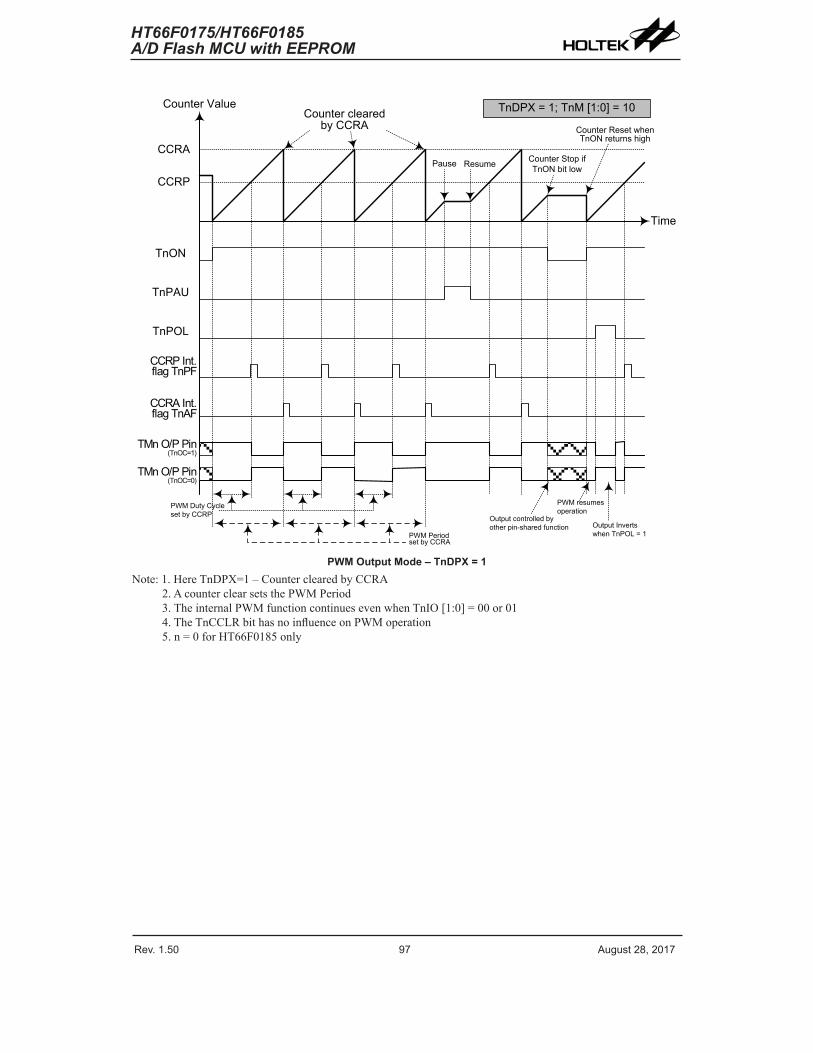
Rev. 1.50 96 ����st ��� �01� Rev. 1.50 9� ����st ��� �01�
HT66F0175/HT66F0185A/D Flash MCU with EEPROM
HT66F0175/HT66F0185A/D Flash MCU with EEPROM
Co�nter Val�e
CCRP
CCR�
TnON
TnP�U
TnPOL
CCRP Int. fla� TnPF
CCR� Int. fla� Tn�F
TMn O/P Pin (TnOC=1)
Time
Co�nter cleared by CCR�
Pa�se Res�me Co�nter Stop if TnON bit low
Co�nter Reset when TnON ret�rns hi�h
TnDPX = 1; TnM [1:0] = 10
PWM D�ty Cycle set by CCRP
PWM res�mes operation
O�tp�t controlled by other pin-shared f�nction O�tp�t Inverts
when TnPOL = 1PWM Period set by CCR�
TMn O/P Pin (TnOC=0)
PWM Output Mode – TnDPX = 1Note:1.HereTnDPX=1–CounterclearedbyCCRA
2.AcounterclearsetsthePWMPeriod3.TheinternalPWMfunctioncontinuesevenwhenTnIO[1:0]=00or014.TheTnCCLRbithasnoinfluenceonPWMoperation5.n=0forHT66F0185only

Rev. 1.50 9� ����st ��� �01� Rev. 1.50 99 ����st ��� �01�
HT66F0175/HT66F0185A/D Flash MCU with EEPROM
HT66F0175/HT66F0185A/D Flash MCU with EEPROM
Single Pulse Output ModeToselectthismode,bitsTnM1andTnM0intheTMnC1registershouldbesetto10respectivelyandalsotheTnIO1andTnIO0bitsshouldbesetto11respectively.TheSinglePulseOutputMode,asthenamesuggests,willgenerateasingleshotpulseontheTMnoutputpin.
ThetriggerforthepulseoutputleadingedgeisalowtohightransitionoftheTnONbit,whichcanbeimplementedusingtheapplicationprogram.HoweverintheSinglePulseMode,theTnONbitcanalsobemadetoautomaticallychangefromlowtohighusingtheexternalTCKnpin,whichwillinturninitiatetheSinglePulseoutput.WhentheTnONbittransitionstoahighlevel,thecounterwillstartrunningandthepulseleadingedgewillbegenerated.TheTnONbitshouldremainhighwhenthepulseisinitsactivestate.ThegeneratedpulsetrailingedgewillbegeneratedwhentheTnONbit isclearedtozero,whichcanbeimplementedusingtheapplicationprogramorwhenacomparematchoccursfromComparatorA.
HoweveracomparematchfromComparatorAwillalsoautomaticallycleartheTnONbitandthusgeneratetheSinglePulseoutputtrailingedge.InthiswaytheCCRAvaluecanbeusedtocontrolthepulsewidth.AcomparematchfromComparatorAwillalsogenerateaTMninterrupt.Thecountercanonlyberesetback tozerowhentheTnONbitchangesfromlowtohighwhenthecounterrestarts.IntheSinglePulseModeCCRPisnotused.TheTnCCLRandTnDPXbitsarenotusedinthisMode.
TnON bit0 à 1
S/W Command SET“TnON”
orTCKn Pin Transition
TnON bit1 à 0
CCR� Trailin� Ed�e
S/W Command CLR“TnON”
orCCR� Compare Match
TPn O�tp�t Pin
P�lse Width = CCR� Val�e
CCR� Leadin� Ed�e
Single Pulse Generation

Rev. 1.50 9� ����st ��� �01� Rev. 1.50 99 ����st ��� �01�
HT66F0175/HT66F0185A/D Flash MCU with EEPROM
HT66F0175/HT66F0185A/D Flash MCU with EEPROM
Co�nter Val�e
CCRP
CCR�
TnON
TnP�U
TnPOL
CCRP Int. Fla� TnPF
CCR� Int. Fla� Tn�F
TMn O/P Pin(TnOC=1)
Time
Co�nter stopped by CCR�
Pa�seRes�me Co�nter Stops
by software
Co�nter Reset when TnON ret�rns hi�h
TnM [1:0] = 10 ; TnIO [1:0] = 11
P�lse Width set by CCR�
O�tp�t Invertswhen TnPOL = 1
No CCRP Interr�pts �enerated
TMn O/P Pin(TnOC=0)
TCKn pin
Software Tri��er
Cleared by CCR� match
TCKn pin Tri��er
��to. set by TCKn pin
Software Tri��er
Software Clear
Software Tri��erSoftware
Tri��er
Single Pulse ModeNote:1.CounterstoppedbyCCRA
2.CCRPisnotused3.ThepulsetriggeredbytheTCKnpinorbysettingtheTnONbithigh4.ATCKnpinactiveedgewillautomaticallysettheTnONbithigh.5.IntheSinglePulseMode,TnIO[1:0]mustbesetto“11”andcannotbechanged.6.n=0forHT66F0185only

Rev. 1.50 100 ����st ��� �01� Rev. 1.50 101 ����st ��� �01�
HT66F0175/HT66F0185A/D Flash MCU with EEPROM
HT66F0175/HT66F0185A/D Flash MCU with EEPROM
Capture Input ModeToselectthismodebitsTnM1andTnM0intheTMnC1registershouldbesetto01respectively.Thismodeenablesexternalsignals tocaptureandstore thepresentvalueof theinternalcounterandcanthereforebeusedforapplicationssuchaspulsewidthmeasurements.TheexternalsignalissuppliedontheTPnpin,whoseactiveedgecanbearisingedge,afallingedgeorbothrisingandfallingedges; theactiveedgetransitiontypeisselectedusingtheTnIO1andTnIO0bits intheTMnC1register.ThecounterisstartedwhentheTnONbitchangesfromlowtohighwhichisinitiatedusingtheapplicationprogram.
WhentherequirededgetransitionappearsontheTPnpinthepresentvalueinthecounterwillbelatchedintotheCCRAregistersandaTMninterruptgenerated.IrrespectiveofwhateventsoccurontheTPnpinthecounterwillcontinuetofreerununtiltheTnONbitchangesfromhightolow.WhenaCCRPcomparematchoccurs thecounterwill resetbacktozero; in thiswaytheCCRPvaluecanbeused tocontrol themaximumcountervalue.WhenaCCRPcomparematchoccursfromComparatorP,aTMninterruptwillalsobegenerated.CountingthenumberofoverflowinterruptsignalsfromtheCCRPcanbeausefulmethodinmeasuringlongpulsewidths.TheTnIO1andTnIO0bitscanselecttheactivetriggeredgeontheTPnpintobearisingedge,fallingedgeorbothedgetypes.IftheTnIO1andTnIO0bitsarebothsethigh,thennocaptureoperationwilltakeplaceirrespectiveofwhathappensontheTPnpin,howeveritmustbenotedthatthecounterwillcontinuetorun.TheTnCCLRandTnDPXbitsarenotusedinthisMode.
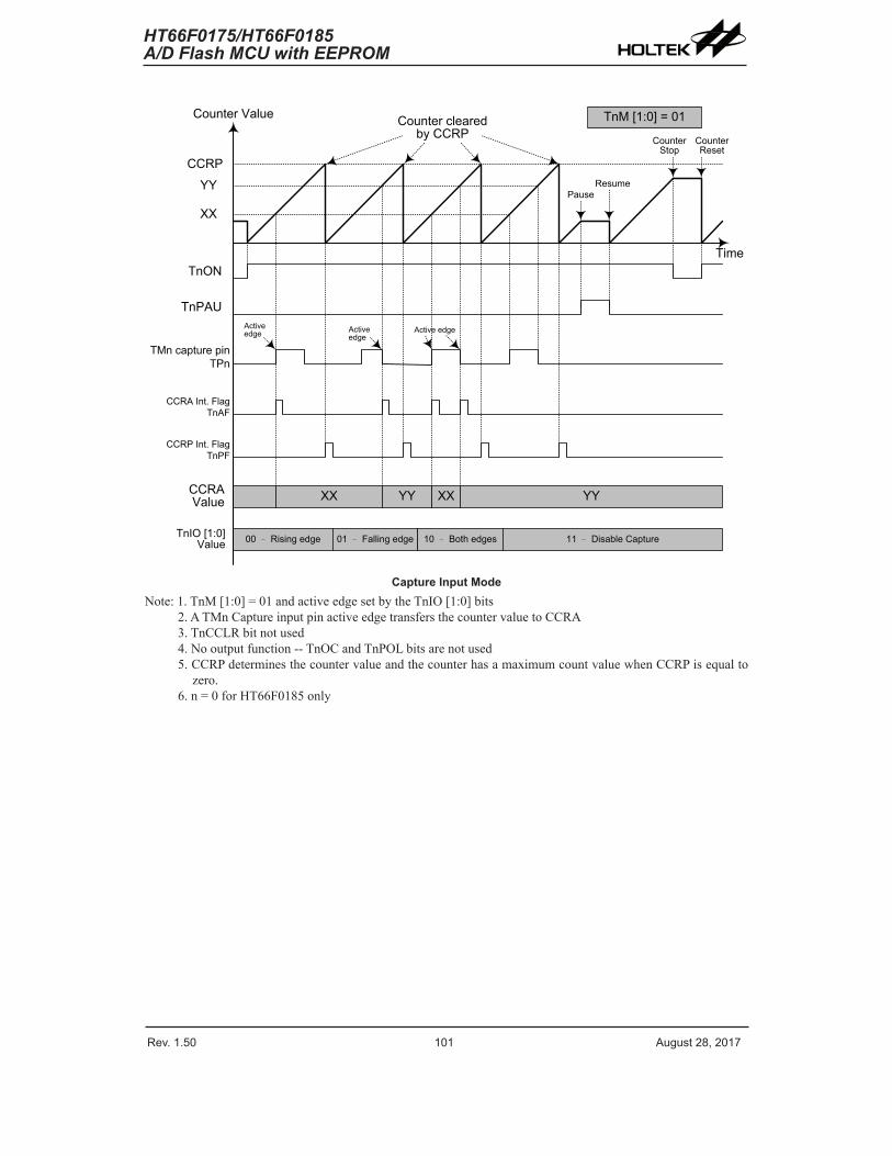
Rev. 1.50 100 ����st ��� �01� Rev. 1.50 101 ����st ��� �01�
HT66F0175/HT66F0185A/D Flash MCU with EEPROM
HT66F0175/HT66F0185A/D Flash MCU with EEPROM
Co�nter Val�e
YY
CCRP
TnON
TnP�U
CCRP Int. Fla� TnPF
CCR� Int. Fla� Tn�F
CCR� Val�e
Time
Co�nter cleared by CCRP
Pa�seRes�me
Co�nter Reset
TnM [1:0] = 01
TMn capt�re pin TPn
XX
Co�nter Stop
TnIO [1:0] Val�e
XX YY XX YY
�ctive ed�e �ctive
ed�e�ctive ed�e
00 – Risin� ed�e 01 – Fallin� ed�e 10 – Both ed�es 11 – Disable Capt�re
Capture Input ModeNote:1.TnM[1:0]=01andactiveedgesetbytheTnIO[1:0]bits
2.ATMnCaptureinputpinactiveedgetransfersthecountervaluetoCCRA3.TnCCLRbitnotused4.Nooutputfunction--TnOCandTnPOLbitsarenotused5.CCRPdeterminesthecountervalueandthecounterhasamaximumcountvaluewhenCCRPisequaltozero.
6.n=0forHT66F0185only

Rev. 1.50 10� ����st ��� �01� Rev. 1.50 103 ����st ��� �01�
HT66F0175/HT66F0185A/D Flash MCU with EEPROM
HT66F0175/HT66F0185A/D Flash MCU with EEPROM
Periodic Type TM – PTMThePeriodicTypeTMcontainsfiveoperatingmodes,whichareCompareMatchOutput,Timer/EventCounter,CaptureInput,SinglePulseOutputandPWMOutputmodes.ThePeriodicTMcanalsobecontrolledwithoneexternalinputpinandcandriveoneexternaloutputpin.
Device TM Core TM No. TM Input Pin TM Output PinHT66F01�5 10-bit PTM TM0� TM1 TCK0� TCK1 TP0� TP1HT66F01�5 10-bit PTM TM1 TCK1 TP1
fSYS
fSYS/4
fH/64fH/16
fTBC
TCKn
000
001
010
011
100
101
110
111
TnCK�~TnCK0
10-bit Co�nt-�p Co�nter
10-bit Comparator P
CCRP
b0~b9
b0~b9
10-bit Comparator �
TnONTnP�U
Comparator � Match
Comparator P Match
Co�nter Clear 01
O�tp�t Control
Polarity Control
Pin Control TPn
TnOC
TnM1� TnM0TnIO1� TnIO0
Tn�F Interr�pt
TnPF Interr�pt
TnPOL TnCP
CCR�
TnCCLR
Ed�eDetector
TnIO1� TnIO0
fH
10
TnC�PTS
Periodic Type TM Block Diagram – n = 0 or 1
Periodic TM OperationThesizeofPeriodicTMis10-bitwideanditscoreisa10-bitcount-upcounterwhichisdrivenbyauserselectableinternalorexternalclocksource.Therearealsotwointernalcomparatorswiththenames,ComparatorAandComparatorP.ThesecomparatorswillcomparethevalueinthecounterwithCCRPandCCRAregisters.TheCCRPandCCRAcomparatorsare10-bitwidewhosevalueisrespectivelycomparedwithallcounterbits.
Theonlywayofchanging thevalueof the10-bitcounterusing theapplicationprogramis toclear thecounterbychanging theTnONbit fromlowtohigh.Thecounterwillalsobeclearedautomaticallybyacounteroverfloworacomparematchwithoneof itsassociatedcomparators.Whentheseconditionsoccur,aTMinterruptsignalwillalsousuallybegenerated.ThePeriodicTypeTMcanoperateinanumberofdifferentoperationalmodes,canbedrivenbydifferentclocksourcesincludinganinputpinandcanalsocontroltheoutputpins.Alloperatingsetupconditionsareselectedusingrelevantinternalregisters.

Rev. 1.50 10� ����st ��� �01� Rev. 1.50 103 ����st ��� �01�
HT66F0175/HT66F0185A/D Flash MCU with EEPROM
HT66F0175/HT66F0185A/D Flash MCU with EEPROM
Periodic Type TM Register DescriptionOveralloperationofthePeriodicTMiscontrolledusingaseriesofregisters.Areadonlyregisterpairexiststostoretheinternalcounter10-bitvalue,whiletworead/writeregisterpairsexisttostoretheinternal10-bitCCRAandCCRPvalue.Theremainingtworegistersarecontrolregisterswhichsetupthedifferentoperatingandcontrolmodes.
Register Name Bit 7 Bit 6 Bit 5 Bit 4 Bit 3 Bit 2 Bit 1 Bit 0
TMnC0 TnP�U TnCK� TnCK1 TnCK0 TnON — — —TMnC1 TnM1 TnM0 TnIO1 TnIO0 TnOC TnPOL TnC�PTS TnCCLRTMnDL D� D6 D5 D4 D3 D� D1 D0TMnDH — — — — — — D9 D�TMn�L D� D6 D5 D4 D3 D� D1 D0TMn�H — — — — — — D9 D�TMnRPL TnRP� TnRP6 TnRP5 TnRP4 TnRP3 TnRP� TnRP1 TnRP0TMnRPH — — — — — — TnRP9 TnRP�
Periodic TM Registers List – n = 0 or 1
TMnDL Register
Bit 7 6 5 4 3 2 1 0Name D� D6 D5 D4 D3 D� D1 D0R/W R R R R R R R RPOR 0 0 0 0 0 0 0 0
Bit7~0 TMnCounterLowByteRegisterbit7~bit0TMn10-bitCounterbit7~bit0
TMnDH Register
Bit 7 6 5 4 3 2 1 0Name — — — — — — D9 D�R/W — — — — — — R RPOR — — — — — — 0 0
Bit7~2 Unimplemented,readas“0”Bit1~0 TMnCounterHighByteRegisterbit1~bit0
TMn10-bitCounterbit9~bit8
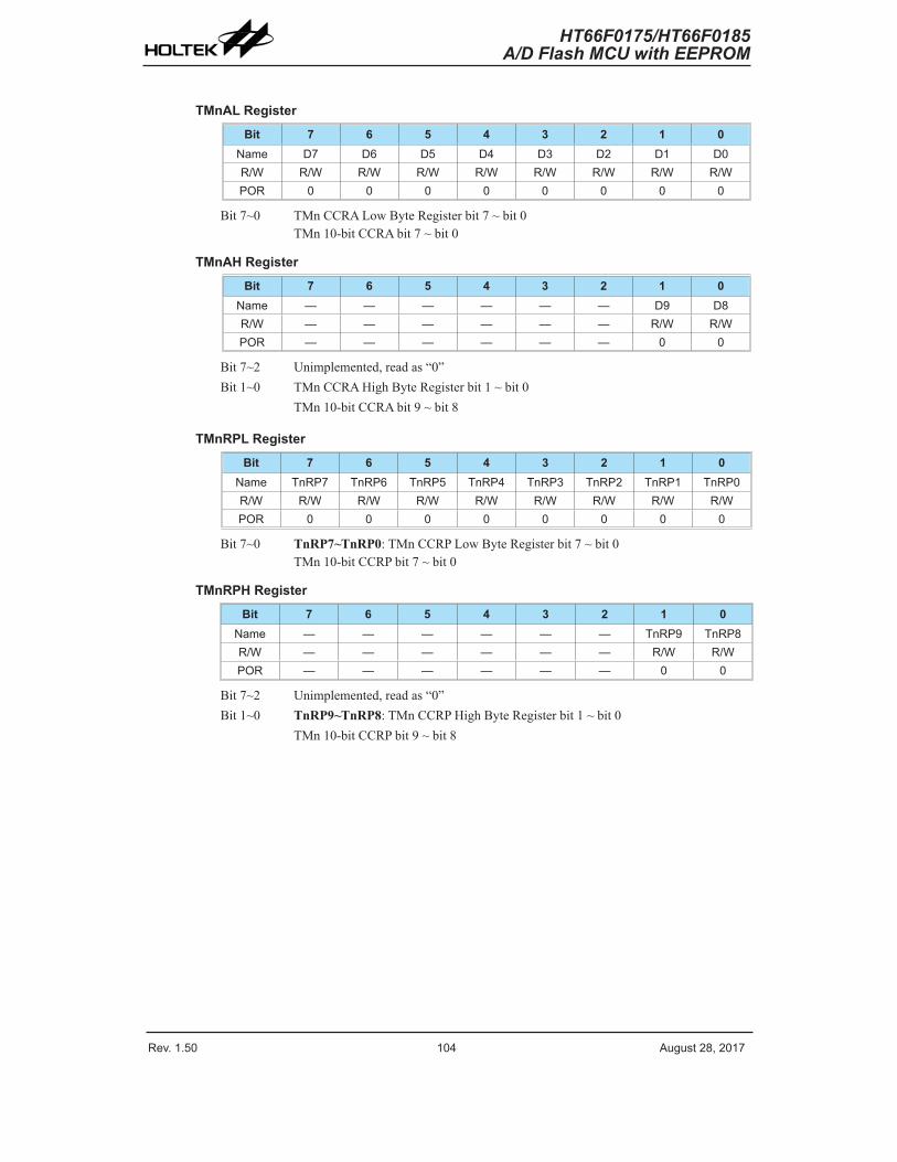
Rev. 1.50 104 ����st ��� �01� Rev. 1.50 105 ����st ��� �01�
HT66F0175/HT66F0185A/D Flash MCU with EEPROM
HT66F0175/HT66F0185A/D Flash MCU with EEPROM
TMnAL Register
Bit 7 6 5 4 3 2 1 0Name D� D6 D5 D4 D3 D� D1 D0R/W R/W R/W R/W R/W R/W R/W R/W R/WPOR 0 0 0 0 0 0 0 0
Bit7~0 TMnCCRALowByteRegisterbit7~bit0TMn10-bitCCRAbit7~bit0
TMnAH Register
Bit 7 6 5 4 3 2 1 0Name — — — — — — D9 D�R/W — — — — — — R/W R/WPOR — — — — — — 0 0
Bit7~2 Unimplemented,readas“0”Bit1~0 TMnCCRAHighByteRegisterbit1~bit0
TMn10-bitCCRAbit9~bit8
TMnRPL Register
Bit 7 6 5 4 3 2 1 0Name TnRP� TnRP6 TnRP5 TnRP4 TnRP3 TnRP� TnRP1 TnRP0R/W R/W R/W R/W R/W R/W R/W R/W R/WPOR 0 0 0 0 0 0 0 0
Bit7~0 TnRP7~TnRP0:TMnCCRPLowByteRegisterbit7~bit0TMn10-bitCCRPbit7~bit0
TMnRPH Register
Bit 7 6 5 4 3 2 1 0Name — — — — — — TnRP9 TnRP�R/W — — — — — — R/W R/WPOR — — — — — — 0 0
Bit7~2 Unimplemented,readas“0”Bit1~0 TnRP9~TnRP8:TMnCCRPHighByteRegisterbit1~bit0
TMn10-bitCCRPbit9~bit8

Rev. 1.50 104 ����st ��� �01� Rev. 1.50 105 ����st ��� �01�
HT66F0175/HT66F0185A/D Flash MCU with EEPROM
HT66F0175/HT66F0185A/D Flash MCU with EEPROM
TMnC0 Register
Bit 7 6 5 4 3 2 1 0Name TnP�U TnCK� TnCK1 TnCK0 TnON — — —R/W R/W R/W R/W R/W R/W — — —POR 0 0 0 0 0 — — —
Bit7 TnPAU:TMnCounterPausecontrol0:Run1:Pause
Thecountercanbepausedbysettingthisbithigh.Clearingthebit tozerorestoresnormalcounteroperation.WheninaPauseconditiontheTMnwillremainpoweredupandcontinuetoconsumepower.Thecounterwillretainitsresidualvaluewhenthisbitchangesfromlowtohighandresumecountingfromthisvaluewhenthebitchangestoalowvalueagain.
Bit6~4 TnCK2~TnCK0:SelectTMnCounterclock000:fSYS/4001:fSYS
010:fH/16011:fH/64100:fTBC101:fH110:TCKnrisingedgeclock111:TCKnfallingedgeclock
ThesethreebitsareusedtoselecttheclocksourcefortheTMn.Theexternalpinclocksourcecanbechosentobeactiveontherisingorfallingedge.TheclocksourcefSYSisthesystemclock,whilefHandfTBCareotherinternalclocks,thedetailsofwhichcanbefoundintheoscillatorsection.
Bit3 TnON:TMnCounterOn/Offcontrol0:Off1:On
Thisbitcontrolstheoverallon/offfunctionoftheTMn.SettingthebithighenablesthecountertorunwhileclearingthebitdisablestheTMn.Clearingthisbit tozerowillstopthecounterfromcountingandturnofftheTMnwhichwillreduceitspowerconsumption.Whenthebitchangesstatefromlowtohightheinternalcountervaluewillbereset tozero,howeverwhenthebitchangesfromhighto low, the internalcounterwillretainitsresidualvalueuntilthebitreturnshighagain.IftheTMnisintheCompareMatchOutputModethentheTMnoutputpinwillberesettoitsinitialcondition,asspecifiedbytheTnOCbit,whentheTnONbitchangesfromlowtohigh.
Bit2~0 Unimplemented,readas“0”
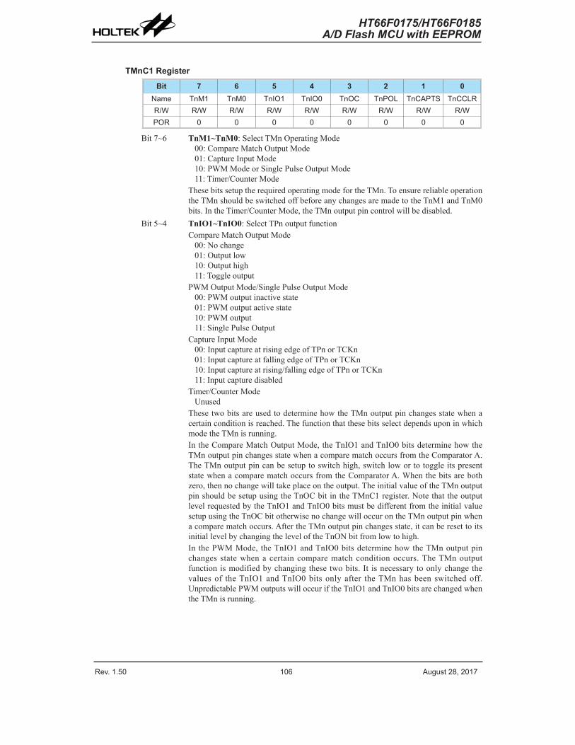
Rev. 1.50 106 ����st ��� �01� Rev. 1.50 10� ����st ��� �01�
HT66F0175/HT66F0185A/D Flash MCU with EEPROM
HT66F0175/HT66F0185A/D Flash MCU with EEPROM
TMnC1 Register
Bit 7 6 5 4 3 2 1 0Name TnM1 TnM0 TnIO1 TnIO0 TnOC TnPOL TnC�PTS TnCCLRR/W R/W R/W R/W R/W R/W R/W R/W R/WPOR 0 0 0 0 0 0 0 0
Bit7~6 TnM1~TnM0:SelectTMnOperatingMode00:CompareMatchOutputMode01:CaptureInputMode10:PWMModeorSinglePulseOutputMode11:Timer/CounterMode
ThesebitssetuptherequiredoperatingmodefortheTMn.ToensurereliableoperationtheTMnshouldbeswitchedoffbeforeanychangesaremadetotheTnM1andTnM0bits.IntheTimer/CounterMode,theTMnoutputpincontrolwillbedisabled.
Bit5~4 TnIO1~TnIO0:SelectTPnoutputfunctionCompareMatchOutputMode00:Nochange01:Outputlow10:Outputhigh11:Toggleoutput
PWMOutputMode/SinglePulseOutputMode00:PWMoutputinactivestate01:PWMoutputactivestate10:PWMoutput11:SinglePulseOutput
CaptureInputMode00:InputcaptureatrisingedgeofTPnorTCKn01:InputcaptureatfallingedgeofTPnorTCKn10:Inputcaptureatrising/fallingedgeofTPnorTCKn11:Inputcapturedisabled
Timer/CounterModeUnused
ThesetwobitsareusedtodeterminehowtheTMnoutputpinchangesstatewhenacertainconditionisreached.ThefunctionthatthesebitsselectdependsuponinwhichmodetheTMnisrunning.IntheCompareMatchOutputMode,theTnIO1andTnIO0bitsdeterminehowtheTMnoutputpinchangesstatewhenacomparematchoccursfromtheComparatorA.TheTMnoutputpincanbesetuptoswitchhigh,switchlowortotoggleitspresentstatewhenacomparematchoccursfromtheComparatorA.Whenthebitsarebothzero,thennochangewilltakeplaceontheoutput.TheinitialvalueoftheTMnoutputpinshouldbesetupusingtheTnOCbit intheTMnC1register.NotethattheoutputlevelrequestedbytheTnIO1andTnIO0bitsmustbedifferentfromtheinitialvaluesetupusingtheTnOCbitotherwisenochangewilloccurontheTMnoutputpinwhenacomparematchoccurs.AftertheTMnoutputpinchangesstate,itcanberesettoitsinitiallevelbychangingtheleveloftheTnONbitfromlowtohigh.In thePWMMode, theTnIO1andTnIO0bitsdeterminehowtheTMnoutputpinchanges statewhenacertaincomparematchconditionoccurs.TheTMnoutputfunctionismodifiedbychangingthesetwobits. It isnecessarytoonlychangethevaluesof theTnIO1andTnIO0bitsonlyafter theTMnhasbeen switchedoff.UnpredictablePWMoutputswilloccuriftheTnIO1andTnIO0bitsarechangedwhentheTMnisrunning.

Rev. 1.50 106 ����st ��� �01� Rev. 1.50 10� ����st ��� �01�
HT66F0175/HT66F0185A/D Flash MCU with EEPROM
HT66F0175/HT66F0185A/D Flash MCU with EEPROM
Bit3 TnOC:TMnTPnOutputcontrolCompareMatchOutputMode0:Initiallow1:Initialhigh
PWMOutputMode/SinglePulseOutputMode0:Activelow1:Activehigh
This is theoutputcontrolbit for theTMnoutputpin. ItsoperationdependsuponwhetherTMnisbeingusedintheCompareMatchOutputModeorinthePWMMode/SinglePulseOutputMode.IthasnoeffectiftheTMnisintheTimer/CounterMode.IntheCompareMatchOutputModeitdeterminesthelogicleveloftheTMnoutputpinbeforeacomparematchoccurs.InthePWMMode/SinglePulseOutputModeitdeterminesifthePWMsignalisactivehighoractivelow.
Bit2 TnPOL:TMnTPnOutputpolaritycontrol0:Non-inverted1:Inverted
ThisbitcontrolsthepolarityoftheTPnoutputpin.WhenthebitissethightheTMnoutputpinwillbeinvertedandnotinvertedwhenthebitiszero.IthasnoeffectiftheTMnisintheTimer/CounterMode.
Bit1 TnCAPTS:TMnCaptureTriggerSourceselection0:FromTPnpin1:FromTCKnpin
Bit0 TnCCLR:TMnCounterClearconditionselection0:ComparatorPmatch1:ComparatorAmatch
Thisbit isused toselect themethodwhichclears thecounter.Remember that thePeriodicTMcontains twocomparators,ComparatorAandComparatorP,eitherofwhichcanbeselectedtoclear the internalcounter.With theTnCCLRbitsethigh,thecounterwillbeclearedwhenacomparematchoccursfromtheComparatorA.Whenthebitislow,thecounterwillbeclearedwhenacomparematchoccursfromtheComparatorPorwithacounteroverflow.AcounteroverflowclearingmethodcanonlybeimplementediftheCCRPbitsareallclearedtozero.TheTnCCLRbitisnotusedinthePWMOutput,SinglePulseOutputorCaptureInputMode.

Rev. 1.50 10� ����st ��� �01� Rev. 1.50 109 ����st ��� �01�
HT66F0175/HT66F0185A/D Flash MCU with EEPROM
HT66F0175/HT66F0185A/D Flash MCU with EEPROM
Periodic Type TM Operation ModesThePeriodicTypeTMcanoperateinoneoffiveoperatingmodes,CompareMatchOutputMode,PWMOutputMode,SinglePulseOutputMode,CaptureInputModeorTimer/CounterMode.TheoperatingmodeisselectedusingtheTnM1andTnM0bitsintheTMnC1register.
Compare Match Output ModeToselectthismode,bitsTnM1andTnM0intheTMnC1register,shouldbesetto00respectively.Inthismodeoncethecounterisenabledandrunningitcanbeclearedbythreemethods.Theseareacounteroverflow,acomparematchfromComparatorAandacomparematchfromComparatorP.WhentheTnCCLRbitislow,therearetwowaysinwhichthecountercanbecleared.OneiswhenacomparematchfromComparatorP, theotheriswhentheCCRPbitsareallzerowhichallowsthecounter tooverflow.HerebothTnAFandTnPFinterruptrequestflagsforComparatorAandComparatorPrespectively,willbothbegenerated.
IftheTnCCLRbitintheTMnC1registerishighthenthecounterwillbeclearedwhenacomparematchoccurs fromComparatorA.However,hereonly theTnAFinterrupt request flagwillbegeneratedevenifthevalueoftheCCRPbitsislessthanthatoftheCCRAregisters.ThereforewhenTnCCLRishighnoTnPFinterruptrequestflagwillbegenerated.IntheCompareMatchOutputMode,theCCRAcannotbesetto“0”.
Asthenameof themodesuggests,afteracomparisonismade, theTMnoutputpinwillchangestate.TheTMnoutputpinconditionhoweveronlychangesstatewhenaTnAFinterruptrequestflagisgeneratedafteracomparematchoccursfromComparatorA.TheTnPFinterruptrequestflag,generatedfromacomparematchoccursfromComparatorP,willhavenoeffectontheTMnoutputpin.ThewayinwhichtheTMnoutputpinchangesstatearedeterminedbytheconditionof theTnIO1andTnIO0bitsintheTMnC1register.TheTMnoutputpincanbeselectedusingtheTnIO1andTnIO0bitstogohigh,togolowortotogglefromitspresentconditionwhenacomparematchoccursfromComparatorA.Theinitialconditionof theTMnoutputpin,whichissetupafter theTnONbitchangesfromlowtohigh,issetupusingtheTnOCbit.NotethatiftheTnIO1andTnIO0bitsarezerothennopinchangewilltakeplace.
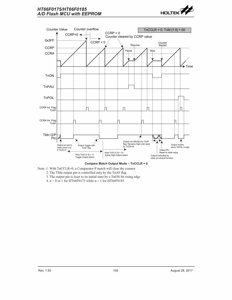
Rev. 1.50 10� ����st ��� �01� Rev. 1.50 109 ����st ��� �01�
HT66F0175/HT66F0185A/D Flash MCU with EEPROM
HT66F0175/HT66F0185A/D Flash MCU with EEPROM
Co�nter Val�e
0x3FF
CCRP
CCR�
TnON
TnP�U
TnPOL
CCRP Int. Fla� TnPF
CCR� Int. Fla� Tn�F
TMn O/P Pin
Time
CCRP=0
CCRP > 0
Co�nter overflowCCRP > 0Co�nter cleared by CCRP val�e
Pa�se
Res�me
Stop
Co�nter Restart
TnCCLR = 0; TnM [1:0] = 00
O�tp�t pin set to initial Level Low if TnOC=0
O�tp�t To��le with Tn�F fla�
Note TnIO [1:0] = 10 �ctive Hi�h O�tp�t selectHere TnIO [1:0] = 11
To��le O�tp�t select
O�tp�t not affected by Tn�F fla�. Remains Hi�h �ntil reset by TnON bit
O�tp�t PinReset to Initial val�e
O�tp�t controlled by other pin-shared f�nction
O�tp�t Invertswhen TnPOL is hi�h
Compare Match Output Mode – TnCCLR = 0Note:1.WithTnCCLR=0,aComparatorPmatchwillclearthecounter
2.TheTMnoutputpiniscontrolledonlybytheTnAFflag3.TheoutputpinisresettoitsinitialstatebyaTnONbitrisingedge4.n=0or1forHT66F0175whilen=1forHT66F0185

Rev. 1.50 110 ����st ��� �01� Rev. 1.50 111 ����st ��� �01�
HT66F0175/HT66F0185A/D Flash MCU with EEPROM
HT66F0175/HT66F0185A/D Flash MCU with EEPROM
Co�nter Val�e
0x3FF
CCRP
CCR�
TnON
TnP�U
TnPOL
CCRP Int. Fla� TnPF
CCR� Int. Fla� Tn�F
TMn O/P Pin
Time
CCR�=0
CCR� = 0Co�nter overflowCCR� > 0 Co�nter cleared by CCR� val�e
Pa�se
Res�me
Stop Co�nter Restart
TnCCLR = 1; TnM [1:0] = 00
O�tp�t pin set to initial Level Low if TnOC=0
O�tp�t To��le with Tn�F fla�
Note TnIO [1:0] = 10 �ctive Hi�h O�tp�t selectHere TnIO [1:0] = 11
To��le O�tp�t select
O�tp�t not affected by Tn�F fla�. Remains Hi�h �ntil reset by TnON bit
O�tp�t PinReset to Initial val�e
O�tp�t controlled by other pin-shared f�nction
O�tp�t Invertswhen TnPOL is hi�h
TnPF not �enerated
No Tn�F fla� �enerated on CCR� overflow
O�tp�t does not chan�e
Compare Match Output Mode - TnCCLR = 1Note:1.WithTnCCLR=1,aComparatorAmatchwillclearthecounter
2.TheTMnoutputpiniscontrolledonlybytheTnAFflag3.TheoutputpinisresettoitsinitialstatebyaTnONbitrisingedge4.ATnPFflagisnotgeneratedwhenTnCCLR=15.n=0or1forHT66F0175whilen=1forHT66F0185
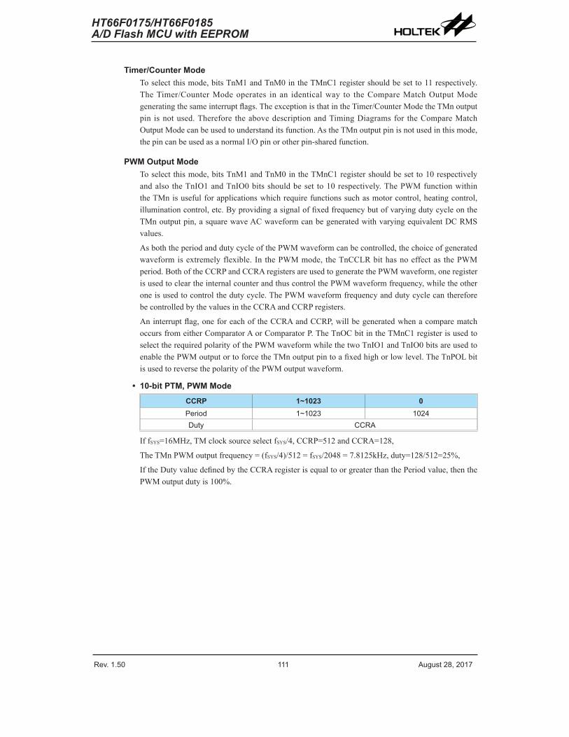
Rev. 1.50 110 ����st ��� �01� Rev. 1.50 111 ����st ��� �01�
HT66F0175/HT66F0185A/D Flash MCU with EEPROM
HT66F0175/HT66F0185A/D Flash MCU with EEPROM
Timer/Counter ModeToselectthismode,bitsTnM1andTnM0intheTMnC1registershouldbesetto11respectively.TheTimer/CounterModeoperates in an identicalway to theCompareMatchOutputModegeneratingthesameinterruptflags.TheexceptionisthatintheTimer/CounterModetheTMnoutputpin isnotused.Therefore theabovedescriptionandTimingDiagramsfor theCompareMatchOutputModecanbeusedtounderstanditsfunction.AstheTMnoutputpinisnotusedinthismode,thepincanbeusedasanormalI/Opinorotherpin-sharedfunction.
PWM Output ModeToselectthismode,bitsTnM1andTnM0intheTMnC1registershouldbesetto10respectivelyandalso theTnIO1andTnIO0bitsshouldbeset to10respectively.ThePWMfunctionwithintheTMnisusefulforapplicationswhichrequirefunctionssuchasmotorcontrol,heatingcontrol,illuminationcontrol,etc.ByprovidingasignaloffixedfrequencybutofvaryingdutycycleontheTMnoutputpin,asquarewaveACwaveformcanbegeneratedwithvaryingequivalentDCRMSvalues.
AsboththeperiodanddutycycleofthePWMwaveformcanbecontrolled,thechoiceofgeneratedwaveformisextremelyflexible. In thePWMmode, theTnCCLRbithasnoeffectas thePWMperiod.BothoftheCCRPandCCRAregistersareusedtogeneratethePWMwaveform,oneregisterisusedtocleartheinternalcounterandthuscontrolthePWMwaveformfrequency,whiletheotheroneisusedtocontrolthedutycycle.ThePWMwaveformfrequencyanddutycyclecanthereforebecontrolledbythevaluesintheCCRAandCCRPregisters.
Aninterruptflag,oneforeachoftheCCRAandCCRP,willbegeneratedwhenacomparematchoccursfromeitherComparatorAorComparatorP.TheTnOCbitintheTMnC1registerisusedtoselecttherequiredpolarityofthePWMwaveformwhilethetwoTnIO1andTnIO0bitsareusedtoenablethePWMoutputortoforcetheTMnoutputpintoafixedhighorlowlevel.TheTnPOLbitisusedtoreversethepolarityofthePWMoutputwaveform.
• 10-bit PTM, PWM Mode
CCRP 1~1023 0Period 1~10�3 10�4D�ty CCR�
IffSYS=16MHz,TMclocksourceselectfSYS/4,CCRP=512andCCRA=128,
TheTMnPWMoutputfrequency=(fSYS/4)/512=fSYS/2048=7.8125kHz,duty=128/512=25%,
IftheDutyvaluedefinedbytheCCRAregisterisequaltoorgreaterthanthePeriodvalue,thenthePWMoutputdutyis100%.
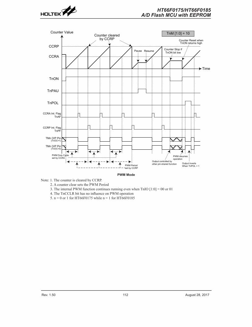
Rev. 1.50 11� ����st ��� �01� Rev. 1.50 113 ����st ��� �01�
HT66F0175/HT66F0185A/D Flash MCU with EEPROM
HT66F0175/HT66F0185A/D Flash MCU with EEPROM
Co�nter Val�e
CCRP
CCR�
TnON
TnP�U
TnPOL
CCRP Int. Fla� TnPF
CCR� Int. Fla� Tn�F
TMn O/P Pin(TnOC=1)
Time
Co�nter cleared by CCRP
Pa�se Res�me Co�nter Stop if TnON bit low
Co�nter Reset when TnON ret�rns hi�h
TnM [1:0] = 10
PWM D�ty Cycle set by CCR�
PWM res�mes operation
O�tp�t controlled by other pin-shared f�nction O�tp�t Inverts
When TnPOL = 1PWM Period set by CCRP
TMn O/P Pin(TnOC=0)
PWM ModeNote:1.ThecounterisclearedbyCCRP.
2.AcounterclearsetsthePWMPeriod3.TheinternalPWMfunctioncontinuesrunningevenwhenTnIO[1:0]=00or014.TheTnCCLRbithasnoinfluenceonPWMoperation5.n=0or1forHT66F0175whilen=1forHT66F0185
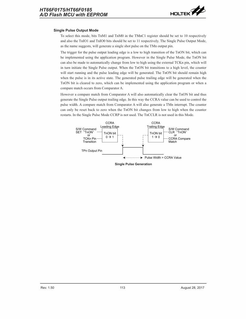
Rev. 1.50 11� ����st ��� �01� Rev. 1.50 113 ����st ��� �01�
HT66F0175/HT66F0185A/D Flash MCU with EEPROM
HT66F0175/HT66F0185A/D Flash MCU with EEPROM
Single Pulse Output ModeToselectthismode,bitsTnM1andTnM0intheTMnC1registershouldbesetto10respectivelyandalsotheTnIO1andTnIO0bitsshouldbesetto11respectively.TheSinglePulseOutputMode,asthenamesuggests,willgenerateasingleshotpulseontheTMnoutputpin.
ThetriggerforthepulseoutputleadingedgeisalowtohightransitionoftheTnONbit,whichcanbeimplementedusingtheapplicationprogram.HoweverintheSinglePulseMode,theTnONbitcanalsobemadetoautomaticallychangefromlowtohighusingtheexternalTCKnpin,whichwillinturninitiatetheSinglePulseoutput.WhentheTnONbittransitionstoahighlevel,thecounterwillstartrunningandthepulseleadingedgewillbegenerated.TheTnONbitshouldremainhighwhenthepulseisinitsactivestate.ThegeneratedpulsetrailingedgewillbegeneratedwhentheTnONbit isclearedtozero,whichcanbeimplementedusingtheapplicationprogramorwhenacomparematchoccursfromComparatorA.
HoweveracomparematchfromComparatorAwillalsoautomaticallycleartheTnONbitandthusgeneratetheSinglePulseoutputtrailingedge.InthiswaytheCCRAvaluecanbeusedtocontrolthepulsewidth.AcomparematchfromComparatorAwillalsogenerateaTMninterrupt.Thecountercanonlyberesetback tozerowhentheTnONbitchangesfromlowtohighwhenthecounterrestarts.IntheSinglePulseModeCCRPisnotused.TheTnCCLRisnotusedinthisMode.
TnON bit0 à 1
S/W Command SET“TnON”
orTCKn Pin Transition
TnON bit1 à 0
CCR� Trailin� Ed�e
S/W Command CLR“TnON”
orCCR� Compare Match
TPn O�tp�t Pin
P�lse Width = CCR� Val�e
CCR� Leadin� Ed�e
Single Pulse Generation
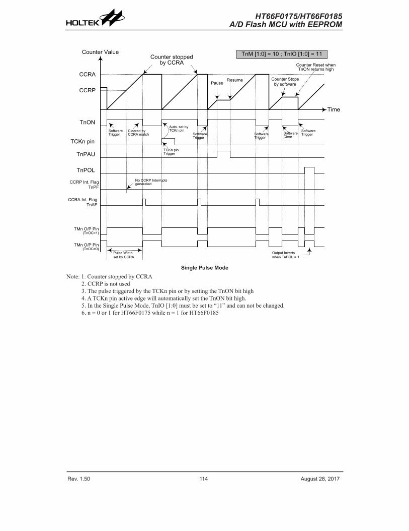
Rev. 1.50 114 ����st ��� �01� Rev. 1.50 115 ����st ��� �01�
HT66F0175/HT66F0185A/D Flash MCU with EEPROM
HT66F0175/HT66F0185A/D Flash MCU with EEPROM
Co�nter Val�e
CCRP
CCR�
TnON
TnP�U
TnPOL
CCRP Int. Fla� TnPF
CCR� Int. Fla� Tn�F
TMn O/P Pin(TnOC=1)
Time
Co�nter stopped by CCR�
Pa�seRes�me Co�nter Stops
by software
Co�nter Reset when TnON ret�rns hi�h
TnM [1:0] = 10 ; TnIO [1:0] = 11
P�lse Width set by CCR�
O�tp�t Invertswhen TnPOL = 1
No CCRP Interr�pts �enerated
TMn O/P Pin(TnOC=0)
TCKn pin
Software Tri��er
Cleared by CCR� match
TCKn pin Tri��er
��to. set by TCKn pin
Software Tri��er
Software Clear
Software Tri��erSoftware
Tri��er
Single Pulse ModeNote:1.CounterstoppedbyCCRA
2.CCRPisnotused3.ThepulsetriggeredbytheTCKnpinorbysettingtheTnONbithigh4.ATCKnpinactiveedgewillautomaticallysettheTnONbithigh.5.IntheSinglePulseMode,TnIO[1:0]mustbesetto“11”andcannotbechanged.6.n=0or1forHT66F0175whilen=1forHT66F0185

Rev. 1.50 114 ����st ��� �01� Rev. 1.50 115 ����st ��� �01�
HT66F0175/HT66F0185A/D Flash MCU with EEPROM
HT66F0175/HT66F0185A/D Flash MCU with EEPROM
Capture Input ModeToselectthismodebitsTnM1andTnM0intheTMnC1registershouldbesetto01respectively.Thismodeenablesexternalsignals tocaptureandstore thepresentvalueof theinternalcounterandcanthereforebeusedforapplicationssuchaspulsewidthmeasurements.TheexternalsignalissuppliedontheTPnorTCKnpin,selectedbytheTnCAPTSbitintheTMnC1register.Theinputpinactiveedgecanbeeitherarisingedge,afallingedgeorbothrisingandfallingedges;theactiveedgetransitiontypeisselectedusingtheTnIO1andTnIO0bitsintheTMnC1register.ThecounterisstartedwhentheTnONbitchangesfromlowtohighwhichis initiatedusing theapplicationprogram.
WhentherequirededgetransitionappearsontheTPnorTCKnpinthepresentvalueinthecounterwillbelatchedintotheCCRAregistersandaTMninterruptgenerated.IrrespectiveofwhateventsoccurontheTPnorTCKnpinthecounterwillcontinuetofreerununtiltheTnONbitchangesfromhightolow.WhenaCCRPcomparematchoccursthecounterwillresetbacktozero;inthiswaytheCCRPvaluecanbeusedtocontrolthemaximumcountervalue.WhenaCCRPcomparematchoccursfromComparatorP,aTMninterruptwillalsobegenerated.CountingthenumberofoverflowinterruptsignalsfromtheCCRPcanbeausefulmethodinmeasuringlongpulsewidths.TheTnIO1andTnIO0bitscanselecttheactivetriggeredgeontheTPnorTCKnpintobearisingedge,fallingedgeorbothedgetypes.IftheTnIO1andTnIO0bitsarebothsethigh,thennocaptureoperationwilltakeplaceirrespectiveofwhathappensontheTPnorTCKnpin,howeveritmustbenotedthatthecounterwillcontinuetorun.
AstheTPnorTCKnpinispinsharedwithotherfunctions,caremustbetakeniftheTMnisintheInputCaptureMode.Thisisbecauseifthepinissetupasanoutput,thenanytransitionsonthispinmaycauseaninputcaptureoperationtobeexecuted.TheTnCCLR,TnOCandTnPOLbitsarenotusedinthisMode.
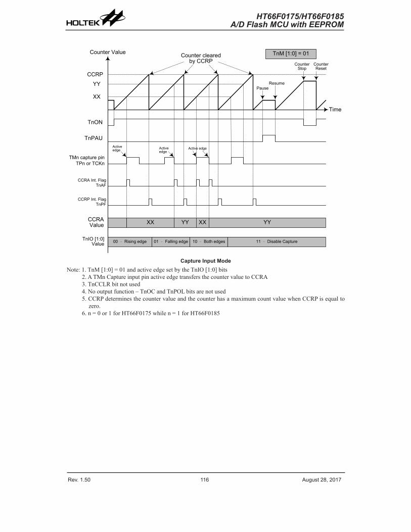
Rev. 1.50 116 ����st ��� �01� Rev. 1.50 11� ����st ��� �01�
HT66F0175/HT66F0185A/D Flash MCU with EEPROM
HT66F0175/HT66F0185A/D Flash MCU with EEPROM
Co�nter Val�e
YY
CCRP
TnON
TnP�U
CCRP Int. Fla� TnPF
CCR� Int. Fla� Tn�F
CCR� Val�e
Time
Co�nter cleared by CCRP
Pa�seRes�me
Co�nter Reset
TnM [1:0] = 01
TMn capt�re pinTPn or TCKn
XX
Co�nter Stop
TnIO [1:0] Val�e
XX YY XX YY
�ctive ed�e �ctive
ed�e�ctive ed�e
00 – Risin� ed�e 01 – Fallin� ed�e 10 – Both ed�es 11 – Disable Capt�re
Capture Input ModeNote:1.TnM[1:0]=01andactiveedgesetbytheTnIO[1:0]bits
2.ATMnCaptureinputpinactiveedgetransfersthecountervaluetoCCRA3.TnCCLRbitnotused4.Nooutputfunction–TnOCandTnPOLbitsarenotused5.CCRPdeterminesthecountervalueandthecounterhasamaximumcountvaluewhenCCRPisequaltozero.
6.n=0or1forHT66F0175whilen=1forHT66F0185
Rev. 1.50 116 ����st ��� �01� Rev. 1.50 11� ����st ��� �01�
HT66F0175/HT66F0185A/D Flash MCU with EEPROM
HT66F0175/HT66F0185A/D Flash MCU with EEPROM
Analog to Digital ConverterTheneedtointerfacetorealworldanalogsignals isacommonrequirementformanyelectronicsystems.However, toproperlyprocess these signalsbyamicrocontroller, theymust firstbeconverted intodigitalsignalsbyA/Dconverters.By integrating theA/Dconversionelectroniccircuitryintothemicrocontroller,theneedforexternalcomponentsisreducedsignificantlywiththecorrespondingfollow-onbenefitsoflowercostsandreducedcomponentspacerequirements.
A/D OverviewThesedevicescontainamulti-channelanalogtodigitalconverterwhichcandirectly interfacetoexternalanalogsignals,suchasthatfromsensorsorothercontrolsignalsandconvertthesesignalsdirectly intoa12-bitdigitalvalue. Italsocanconvert the internalsignals,suchas theBandgapreferencevoltage,intoa12-bitdigitalvalue.TheexternalorinternalanalogsignaltobeconvertedisdeterminedbytheSAINS2~SAINS0bitstogetherwiththeSACS2~SACS0bits.Notethatwhentheexternalandinternalanalogsignalsaresimultaneouslyselectedtobeconverted,theinternalanalogsignalwillhavethepriority.Inthemeantimetheexternalanalogsignalwilltemporarilybeswitchedoffuntil the internalanalogsignal isdeselected.Moredetailed informationabout theA/Dinputsignal isdescribedin the“A/DConverterControlRegisters”and“A/DConverterInputSignal”sectionsrespectively.
TheaccompanyingblockdiagramshowstheinternalstructureoftheA/Dconvertertogetherwithitsassociatedregisters.
Device External Input Channel Internal Analog Signals A/D Signal Select Bits
HT66F01�5 �N0~�N� VDD� VDD/�� VDD/4� VR� VR/�� VR/4 S�INS�~S�INS0; S�CS�~S�CS0
HT66F01�5 �N0~�N� VDD� VDD/�� VDD/4� VR� VR/�� VR/4 S�INS�~S�INS0; S�CS�~S�CS0
�CE�~�CE0S�CS�~S�CS0
S�INS�~S�INS0
�/D Converter
ST�RT �DBZ �DCEN
VSS�/D Clock
÷ �N
(N=0~�)
fSYS
S�CKS�~S�CKS0
VDD
�DCEN
S�DOL
S�DOH
�N0�N1
�N� �/D Reference Volta�e
�/D DataRe�isters
VDD
VDD/�VDD/4VR
VR/�VR/4
�DRFS
PG�VRI
VREFI
VBG
(Gain=1~4)
S�VRS3~S�VRS0
�DPG�EN
VREF
VR
VDD
VREFPS
VREFIPS
A/D Converter Structure
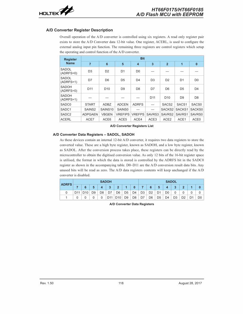
Rev. 1.50 11� ����st ��� �01� Rev. 1.50 119 ����st ��� �01�
HT66F0175/HT66F0185A/D Flash MCU with EEPROM
HT66F0175/HT66F0185A/D Flash MCU with EEPROM
A/D Converter Register DescriptionOveralloperationof theA/Dconverteriscontrolledusingsixregisters.AreadonlyregisterpairexiststostoretheA/DConverterdata12-bitvalue.Oneregister,ACERL,isusedtoconfiguretheexternalanaloginputpinfunction.TheremainingthreeregistersarecontrolregisterswhichsetuptheoperatingandcontrolfunctionoftheA/Dconverter.
Register Name
Bit
7 6 5 4 3 2 1 0S�DOL (�DRFS=0) D3 D� D1 D0 — — — —
S�DOL (�DRFS=1) D� D6 D5 D4 D3 D� D1 D0
S�DOH (�DRFS=0) D11 D10 D9 D� D� D6 D5 D4
S�DOH (�DRFS=1) — — — — D11 D10 D9 D�
S�DC0 ST�RT �DBZ �DCEN �DRFS — S�CS� S�CS1 S�CS0S�DC1 S�INS� S�INS10 S�INS0 — — S�CKS� S�CKS1 S�CKS0S�DC� �DPG�EN VBGEN VREFIPS VREFPS S�VRS3 S�VRS� S�VRS1 S�VRS0�CERL �CE� �CE6 �CE5 �CE4 �CE3 �CE� �CE1 �CE0
A/D Converter Registers List
A/D Converter Data Registers – SADOL, SADOHAsthesedevicescontainaninternal12-bitA/Dconverter,itrequirestwodataregisterstostoretheconvertedvalue.Theseareahighbyteregister,knownasSADOH,andalowbyteregister,knownasSADOL.After theconversionprocess takesplace, theseregisterscanbedirectlyreadbythemicrocontrollertoobtainthedigitisedconversionvalue.Asonly12bitsofthe16-bitregisterspaceisutilised, theformat inwhichthedata isstorediscontrolledbytheADRFSbit in theSADC0registerasshownintheaccompanyingtable.D0~D11aretheA/Dconversionresultdatabits.Anyunusedbitswillbereadaszero.TheA/Ddataregisterscontentswillkeepunchangedif theA/Dconverterisdisabled.
ADRFSSADOH SADOL
7 6 5 4 3 2 1 0 7 6 5 4 3 2 1 00 D11 D10 D9 D� D� D6 D5 D4 D3 D� D1 D0 0 0 0 01 0 0 0 0 D11 D10 D9 D� D� D6 D5 D4 D3 D� D1 D0
A/D Converter Data Registers

Rev. 1.50 11� ����st ��� �01� Rev. 1.50 119 ����st ��� �01�
HT66F0175/HT66F0185A/D Flash MCU with EEPROM
HT66F0175/HT66F0185A/D Flash MCU with EEPROM
A/D Converter Control Registers – SADC0, SADC1, SADC2, ACERLTocontrolthefunctionandoperationoftheA/Dconverter,threecontrolregistersknownasSADC0,SADC1andSADC2areprovided.These8-bitregistersdefinefunctionssuchas theselectionofwhichanalogchannel isconnected to the internalA/Dconverter, thedigitiseddata format, theA/DclocksourceaswellascontrollingthestartfunctionandmonitoringtheA/Dconverterbusystatus.Asthesedevicescontainonlyoneactualanalogtodigitalconverterhardwarecircuit,eachof theexternalandinternalanalogsignalsmustberoutedto theconverter.TheSACS2~SACS0bits in theSADC0registerareusedtodeterminewhichexternalchannel input isselected tobeconverted.TheSAINS2~SAINS0bitsintheSADC1registerareusedtodeterminethattheanalogsignaltobeconvertedcomesfromtheinternalanalogsignalorexternalanalogchannelinput.IftheSAINS2~SAINS0bitsaresetto“000”or“100”,theexternalanalogchannelinputwillbeselectedtobeconvertedandtheSACS2~SACS0bitscandeterninewhichexternalchannel isselectedtobeconverted.IftheSAINS2~SAINS0bitsaresettoanyothervaluesexcept“000”and“100”,oneoftheinternalanalogsignalscanbeselectedtobeconverted.TheinternalanalogsignalscanbederivedfromtheA/Dconvertersupplypower,VDD,orinternalreferencevoltage,VR,withaspecificratioof1,1/2or1/4.Iftheinternalanalogsignalisselectedtobeconverted,theexternalchannelsignalinputwillautomaticallybeswitchedofftoavoidthesignalcontention.
SAINS [2:0] SACS [2:0] Input Signals Description000� 100 000~111 �N0~�N� External channel analo� inp�t
001 xxx VDD �/D converter power s�pply volta�e010 xxx VDD/� �/D converter power s�pply volta�e/�011 xxx VDD/4 �/D converter power s�pply volta�e/4101 xxx VR Internal reference volta�e110 xxx VR/� Internal reference volta�e/�111 xxx VR/4 Internal reference volta�e/4
A/D Converter Input Signal Selection
Theanaloginputpinfunctionselectionbits in theACERLregisterdeterminewhichpinsonI/OPortsareusedasexternalanalogchannelsfortheA/DconverterinputandwhichpinsarenottobeusedastheA/Dconverterinput.WhenthepinisselectedtobeanA/Dinput,itsoriginalfunctionwhetherit isanI/Oorotherpin-sharedfunctionswillberemoved.Inaddition,anyinternalpull-highresistorconnectedtothepinwillbeautomaticallyremovedifthepinisselectedtobeanA/Dconverterinput.

Rev. 1.50 1�0 ����st ��� �01� Rev. 1.50 1�1 ����st ��� �01�
HT66F0175/HT66F0185A/D Flash MCU with EEPROM
HT66F0175/HT66F0185A/D Flash MCU with EEPROM
• SADC0 Register
Bit 7 6 5 4 3 2 1 0Name ST�RT �DBZ �DCEN �DRFS — S�CS� S�CS1 S�CS0R/W R/W R R/W R/W — R/W R/W R/WPOR 0 0 0 0 — 0 0 0
Bit7 START:StarttheA/DConversion0→1→0:Start
ThisbitisusedtoinitiateanA/Dconversionprocess.Thebitisnormallylowbutifsethighandthenclearedlowagain,theA/Dconverterwillinitiateaconversionprocess.
Bit6 ADBZ:A/DConverterbusyflag0:NoA/Dconversionisinprogress1:A/Dconversionisinprogress
ThisreadonlyflagisusedtoindicatewhethertheA/Dconversionis inprogressornot.WhentheSTARTbitissetfromlowtohighandthentolowagain,theADBZflagwillbesetto1toindicatethattheA/Dconversionisinitiated.TheADBZflagwillbeclearedto0aftertheA/Dconversioniscomplete.
Bit5 ADCEN:A/DConverterfunctionenablecontrol0:Disable1:Enable
Thisbitcontrols theA/Dinternal function.Thisbitshouldbeset toone toenabletheA/Dconverter.If thebit isset low,thentheA/Dconverterwillbeswitchedoffreducingthedevicepowerconsumption.WhentheA/Dconverterfunctionisdisabled,thecontentsoftheA/Ddataregisterpair,SADOH/SADOL,willkeepunchanged.
Bit4 ADRFS:A/Dconversiondataformatselect0:A/Dconverterdataformat→SADOH=D[11:4];SADOL=D[3:0]1:A/Dconverterdataformat→SADOH=D[11:8];SADOL=D[7:0]
Thisbitcontrols theformatof the12-bitconvertedA/Dvaluein thetwoA/Ddataregisters.DetailsareprovidedintheA/Dconverterdataregistersection.
Bit3 Unimplemented,readas“0”Bit2~0 SACS2~SACS0:A/Dconverterexternalanaloginputchannelselect
000:AN0001:AN1010:AN2011:AN3100:AN4101:AN5110:AN6111:AN7

Rev. 1.50 1�0 ����st ��� �01� Rev. 1.50 1�1 ����st ��� �01�
HT66F0175/HT66F0185A/D Flash MCU with EEPROM
HT66F0175/HT66F0185A/D Flash MCU with EEPROM
• SADC1 Register
Bit 7 6 5 4 3 2 1 0Name S�INS� S�INS10 S�INS0 — — S�CKS� S�CKS1 S�CKS0R/W R/W R/W R/W — — R/W R/W R/WPOR 0 0 0 — — 0 0 0
Bit7~5 SAINS2~SAINS0:A/DConverterinputsignalselect000,100:Externalsignal–Externalanalogchannelinput001:Internalsignal–InternalA/DconverterpowersupplyvoltageVDD
010:Internalsignal–InternalA/DconverterpowersupplyvoltageVDD/2011:Internalsignal–InternalA/DconverterpowersupplyvoltageVDD/4101:Internalsignal–InternalreferencevoltageVR
110:Internalsignal–InternalreferencevoltageVR/2111:Internalsignal–InternalreferencevoltageVR/4
Whentheinternalanalogsignalisselectedtobeconverted,theexternalchannelinputsignalwillautomaticallybeswitchedoffregardlessof theSACS2~SACS0bitfieldvalue.TheinternalreferencevoltagecanbederivedfromvarioussourcesselectedusingtheSAVRS3~SAVRS0bitsintheSADC2register.
Bit4~3 Unimplemented,readas“0”Bit2~0 SACKS2~SACKS0:A/Dconversionclocksourceselect
000:fSYS
001:fSYS/2010:fSYS/4011:fSYS/8100:fSYS/16101:fSYS/32110:fSYS/64111:fSYS/128
ThesebitsareusedtoselecttheclocksourcefortheA/Dconverter.

Rev. 1.50 1�� ����st ��� �01� Rev. 1.50 1�3 ����st ��� �01�
HT66F0175/HT66F0185A/D Flash MCU with EEPROM
HT66F0175/HT66F0185A/D Flash MCU with EEPROM
• SADC2 Register
Bit 7 6 5 4 3 2 1 0Name �DPG�EN VBGEN VREFIPS VREFPS S�VRS3 S�VRS� S�VRS1 S�VRS0R/W R/W R/W R/W R/W R/W R/W R/W R/WPOR 0 0 0 0 0 0 0 0
Bit7 ADPGAEN:A/DconverterPGAfunctionenablecontrol0:Disable1:Enable
Thisbitcontrols theinternalPGAfunctiontoprovidevariousreferencevoltagefortheA/Dconverter.Whenthebitissethigh,theinternalreferencevoltage,VR,canbeusedastheinternalconvertedsignalorreferencevoltagebytheA/Dconverter.IftheinternalreferencevoltageisnotusedbytheA/Dconverter, thenthePGAfunctionshouldbeproperlyconfiguredtoconservepower.
Bit6 VBGEN:InternalBandgapreferencevoltageenablecontrol0:Disable1:Enable
Thisbitcontrols the internalBandgapcircuiton/offfunctionto theA/Dconverter.When thebit is sethigh, theBandgap referencevoltagecanbeusedby theA/Dconverter. If theBandgapreferencevoltage isnotusedby theA/DconverterandtheLVDorLVRfunction isdisabled, then thebandgap referencecircuitwillbeautomaticallyswitchedoff toconservepower.WhentheBandgapreferencevoltageisswitchedonforusebytheA/Dconverter,a time,tBGS,shouldbeallowedfortheBandgapcircuittostabilisebeforeimplementinganA/Dconversion.
Bit5 VREFIPS:VREFIpinselectionbit0:Disable–VREFIpinisnotselected1:Enable–VREFIpinisselected
Bit4 VREFPS:VREFpinselectionbit0:Disable–VREFpinisnotselected1:Enable–VREFpinisselected
Bit3~0 SAVRS3~SAVRS0:A/DConverterreferencevoltageselect0000:VDD
0001:VREFI
0010:VREFI×20011:VREFI×30100:VREFI×41001:Reserved,cannotbeused.1010:VBG×21011:VBG×31100:VBG×4Others:VDD
When theA/Dconverter referencevoltagesource is selected toderive from theinternalVBGvoltage, thereferencevoltagewhichcomesfromtheexternalVDDorVREFIpinwillbeautomaticallyswitchedoff.

Rev. 1.50 1�� ����st ��� �01� Rev. 1.50 1�3 ����st ��� �01�
HT66F0175/HT66F0185A/D Flash MCU with EEPROM
HT66F0175/HT66F0185A/D Flash MCU with EEPROM
• ACERL Register
Bit 7 6 5 4 3 2 1 0Name �CE� �CE6 �CE5 �CE4 �CE3 �CE� �CE1 �CE0R/W R/W R/W R/W R/W R/W R/W R/W R/WPOR 1 1 1 1 1 1 1 1
Bit7 ACE7:DefinePB3isA/Dinputornot 0:NotA/Dinput 1:A/Dinput,AN7
Bit6 ACE6:DefinePA7isA/Dinputornot 0:NotA/Dinput 1:A/Dinput,AN6
Bit5 ACE5:DefinePA6isA/Dinputornot 0:NotA/Dinput 1:A/Dinput,AN5
Bit4 ACE4:DefinePA5isA/Dinputornot 0:NotA/Dinput 1:A/Dinput,AN4
Bit3 ACE3:DefinePA4isA/Dinputornot 0:NotA/Dinput 1:A/Dinput,AN3
Bit2 ACE2:DefinePB2isA/Dinputornot 0:NotA/Dinput 1:A/Dinput,AN2
Bit1 ACE1:DefinePB1isA/Dinputornot 0:NotA/Dinput 1:A/Dinput,AN1
Bit0 ACE0:DefinePB0isA/Dinputornot 0:NotA/Dinput 1:A/Dinput,AN0

Rev. 1.50 1�4 ����st ��� �01� Rev. 1.50 1�5 ����st ��� �01�
HT66F0175/HT66F0185A/D Flash MCU with EEPROM
HT66F0175/HT66F0185A/D Flash MCU with EEPROM
A/D Input PinsAlloftheA/Danaloginputpinsarepin-sharedwiththeI/Opinsaswellasotherfunctions.Thecorrespondingpin-sharedfunctionselectionbits intheACERLregisterdeterminewhichexternalinputpinsareselectedasA/Dconverteranalogchannel inputsorother functionalpins. If thecorrespondingpinissetuptobeanA/Dconverteranalogchannelinput,theoriginalpinfunctionswillbedisabled.Inthisway,pinscanbechangedunderprogramcontroltochangetheirfunctionbetweenA/Dinputsandotherfunctions.Allpull-highresistors,whicharesetupthroughregisterprogramming,willbeautomaticallydisconnectedif thepinsaresetupasA/Dinputs.NotethatitisnotnecessarytofirstsetuptheA/DpinasaninputintheportcontrolregistertoenabletheA/DinputaswhentherelevantA/DinputfunctionselectionbitsenableanA/Dinput,thestatusoftheportcontrolregisterwillbeoverridden.
TheA/Dconverterhasitsownreferencevoltageinputpin,VREFI.However,thereferencevoltagecanalsobesuppliedfromthepowersupplypinoran internalBandgapcircuit,achoicewhichismadethroughtheSAVRS3~SAVRS0bits in theSADC2register.TheselectedA/DreferencevoltagecanbeoutputontheVREFpin.TheanaloginputvaluesmustnotbeallowedtoexceedthevalueofVREF.NotethattheVREFIorVREFpinfunctionselectionbitintheSADC2registermustbeproperlyconfiguredbeforethereferencevoltagepinfunctionisused.
A/D Reference VoltageThereferencevoltagesupplytotheA/DConvertercanbesuppliedfromthepositivepowersupplypin,VDD,anexternalreferencesourcesuppliedonpinVREFIoraninternalreferencesourcederivedfromtheBandgapcircuit.ThentheselectedreferencevoltagesourcecanbeamplifiedthroughaprogrammablegainamplifierexceptthevoltagesourcedfromVDD.ThePGAgaincanbeequalto1,2,3or4.ThedesiredselectionismadeusingtheSAVRS3~SAVRS0bitsintheSADC2registerandrelevantpin-sharedfunctionselectionbits.NotethatthedesiredselectedreferencevoltagewillbeoutputontheVREFpinwhichispin-sharedwithotherfunctions.AstheVREFIandVREFpinsbotharepin-sharedwithotherfunctions,whentheVREFIorVREFpinisselectedasthereferencevoltagesupplypin, theVREFIorVREFpin-shared functionselectionbit shouldbeproperlyconfiguredtodisableotherpin-sharedfunctions.
A/D OperationTheSTARTbitintheSADC0registerisusedtostarttheADconversion.Whenthemicrocontrollersets thisbit fromlowtohighandthenlowagain,ananalogtodigitalconversioncyclewillbeinitiated.
TheADBZbitintheSADC0registerisusedtoindicatewhethertheanalogtodigitalconversionprocessisinprogressornot.Thisbitwillbeautomaticallysetto1bythemicrocontrollerafteranA/Dconversionissuccessfullyinitiated.WhentheA/Dconversioniscomplete,theADBZwillbeclearedto0.Inaddition, thecorrespondingA/Dinterruptrequestflagwillbeset in theinterruptcontrolregister,andif thecorresponding interruptcontrolbitsareenabled,an internal interruptsignalwillbegenerated.ThisA/Dinternal interruptsignalwilldirect theprogramflowto theassociatedA/Dinternalinterruptaddressforprocessing.IftheA/Dinternalinterruptisdisabled,themicrocontrollercanpolltheADBZbitintheSADC0registertocheckwhetherithasbeenclearedasanalternativemethodofdetectingtheendofanA/Dconversioncycle.

Rev. 1.50 1�4 ����st ��� �01� Rev. 1.50 1�5 ����st ��� �01�
HT66F0175/HT66F0185A/D Flash MCU with EEPROM
HT66F0175/HT66F0185A/D Flash MCU with EEPROM
TheclocksourcefortheA/Dconverter,whichoriginatesfromthesystemclockfSYS,canbechosentobeeither fSYSorasubdividedversionof fSYS.Thedivisionratiovalue isdeterminedby theSACKS2~SACKS0bitsintheSADC1register.AlthoughtheA/DclocksourceisdeterminedbythesystemclockfSYSandbybitsSACKS2~SACKS0,therearesomelimitationsonthemaximumA/Dclocksourcespeedthatcanbeselected.AstherecommendedrangeofpermissibleA/Dclockperiod,tADCK,isfrom0.5μsto10μs,caremustbetakenforsystemclockfrequencies.Forexample,asthesystemclockoperatesatafrequencyof8MHz,theSACKS2~SACKS0bitsshouldnotbesetto000,001or111.DoingsowillgiveA/DclockperiodsthatarelessthantheminimumA/Dclockperiodwhichmayresult ininaccurateA/Dconversionvalues.Refertothefollowingtableforexamples,wherevaluesmarkedwithanasterisk*showwhere,dependinguponthedevices,specialcaremustbetaken,asthevaluesmaybelessthanthespecifiedminimumA/DClockPeriod.
fSYS
A/D Clock Period (tADCK)
SACKS[2:0]= 000(fSYS)
SACKS[2:0]= 001(fSYS/2)
SACKS[2:0]= 010(fSYS/4)
SACKS[2:0]= 011
(fSYS/8)
SACKS[2:0]= 100
(fSYS/16)
SACKS[2:0]= 101
(fSYS/32)
SACKS[2:0]= 110
(fSYS/64)
SACKS[2:0]= 111
(fSYS/128)1 MHz 1μs 2μs 4μs 8μs 16μs * 32μs * 64μs * 128μs *� MHz 500ns 1μs 2μs 4μs 8μs 16μs * 32μs * 64μs *4 MHz 250ns * 500ns 1μs 2μs 4μs 8μs 16μs * 32μs *� MHz 125ns * 250ns * 500ns 1μs 2μs 4μs 8μs 16μs *
1� MHz 83ns * 167ns * 333ns * 66�ns 1.33μs 2.67μs 5.33μs 10.67μs *16 MHz 62.5ns * 125ns * 250ns * 500ns 1μs 2μs 4μs 8μs�0 MHz 50ns * 100ns * 200ns * 400ns * �00ns 1.6μs 3.2μs 6.4μs
A/D Clock Period Examples
Controlling thepoweron/off functionof theA/Dconvertercircuitry is implementedusing theADCENbitintheSADC0register.ThisbitmustbesethightopowerontheA/Dconverter.WhentheADCENbit issethigh topoweron theA/Dconverter internalcircuitry,acertaindelay,asindicatedin the timingdiagram,mustbeallowedbeforeanA/Dconversionis initiated.EvenifnopinsareselectedforuseasA/Dinputs,iftheADCENbitishigh,thensomepowerwillstillbeconsumed.InpowerconsciousapplicationsitisthereforerecommendedthattheADCENissetlowtoreducepowerconsumptionwhentheA/Dconverterfunctionisnotbeingused.
Conversion Rate and Timing DiagramAcompleteA/Dconversioncontains twoparts,data samplinganddataconversion.ThedatasamplingwhichisdefinedastADStakes4A/Dclockcyclesandthedataconversiontakes12A/Dclockcycles.Thereforeatotalof16A/DclockcyclesforanA/DconversionwhichisdefinedastADCarenecessary.
MaximumsingleA/Dconversionrate=A/Dclockperiod/16(1)
Theaccompanyingdiagramshowsgraphicallythevariousstagesinvolvedinananalogtodigitalconversionprocessanditsassociatedtiming.AfteranA/Dconversionprocesshasbeeninitiatedby theapplicationprogram, themicrocontroller internalhardwarewillbegin tocarryout theconversion,duringwhichtimetheprogramcancontinuewithotherfunctions.ThetimetakenfortheA/Dconversionis16tADCKclockcycleswheretADCKisequaltotheA/Dclockperiod.
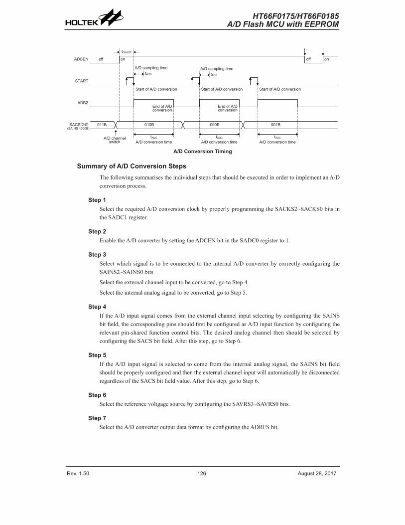
Rev. 1.50 1�6 ����st ��� �01� Rev. 1.50 1�� ����st ��� �01�
HT66F0175/HT66F0185A/D Flash MCU with EEPROM
HT66F0175/HT66F0185A/D Flash MCU with EEPROM
�DCEN
ST�RT
�DBZ
S�CS[�:0]
off on off on
tON�ST
t�DS
�/D samplin� timet�DS
�/D samplin� time
Start of �/D conversion Start of �/D conversion Start of �/D conversion
End of �/D conversion
End of �/D conversion
t�DC
�/D conversion timet�DC
�/D conversion timet�DC
�/D conversion time
011B 010B 000B 001B
�/D channel switch
(S�INS =000B)
A/D Conversion Timing
Summary of A/D Conversion StepsThefollowingsummarisestheindividualstepsthatshouldbeexecutedinordertoimplementanA/Dconversionprocess.
Step 1SelecttherequiredA/DconversionclockbyproperlyprogrammingtheSACKS2~SACKS0bitsintheSADC1register.
Step 2EnabletheA/DconverterbysettingtheADCENbitintheSADC0registerto1.
Step 3Selectwhichsignal is tobeconnectedtotheinternalA/DconverterbycorrectlyconfiguringtheSAINS2~SAINS0bits
Selecttheexternalchannelinputtobeconverted,gotoStep4.
Selecttheinternalanalogsignaltobeconverted,gotoStep5.
Step 4IftheA/DinputsignalcomesfromtheexternalchannelinputselectingbyconfiguringtheSAINSbitfield,thecorrespondingpinsshouldfirstbeconfiguredasA/Dinputfunctionbyconfiguringtherelevantpin-sharedfunctioncontrolbits.Thedesiredanalogchannel thenshouldbeselectedbyconfiguringtheSACSbitfield.Afterthisstep,gotoStep6.
Step 5If theA/Dinputsignal isselected tocomefromthe internalanalogsignal, theSAINSbit fieldshouldbeproperlyconfiguredandthentheexternalchannelinputwillautomaticallybedisconnectedregardlessoftheSACSbitfieldvalue.Afterthisstep,gotoStep6.
Step 6SelectthereferencevoltgagesourcebyconfiguringtheSAVRS3~SAVRS0bits.
Step 7SelecttheA/DconverteroutputdataformatbyconfiguringtheADRFSbit.
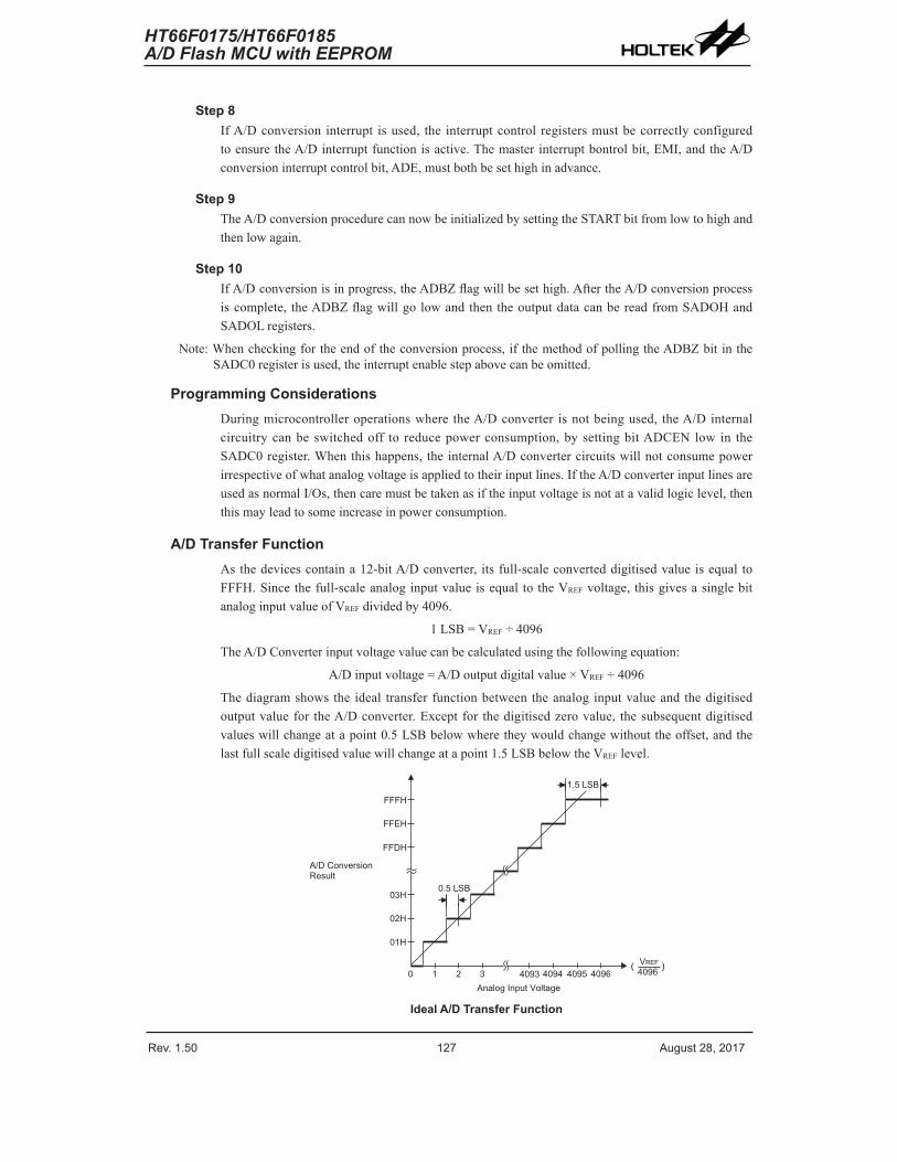
Rev. 1.50 1�6 ����st ��� �01� Rev. 1.50 1�� ����st ��� �01�
HT66F0175/HT66F0185A/D Flash MCU with EEPROM
HT66F0175/HT66F0185A/D Flash MCU with EEPROM
Step 8IfA/Dconversion interrupt isused, the interruptcontrol registersmustbecorrectlyconfiguredtoensuretheA/Dinterruptfunctionisactive.Themasterinterruptbontrolbit,EMI,andtheA/Dconversioninterruptcontrolbit,ADE,mustbothbesethighinadvance.
Step 9TheA/DconversionprocedurecannowbeinitializedbysettingtheSTARTbitfromlowtohighandthenlowagain.
Step 10IfA/Dconversionisinprogress,theADBZflagwillbesethigh.AftertheA/Dconversionprocessiscomplete, theADBZflagwillgolowandthentheoutputdatacanbereadfromSADOHandSADOLregisters.
Note:Whencheckingfortheendoftheconversionprocess,ifthemethodofpollingtheADBZbitintheSADC0registerisused,theinterruptenablestepabovecanbeomitted.
Programming ConsiderationsDuringmicrocontrolleroperationswhere theA/Dconverter isnotbeingused, theA/Dinternalcircuitrycanbeswitchedoff to reducepowerconsumption,bysettingbitADCENlow in theSADC0register.Whenthishappens, theinternalA/Dconvertercircuitswillnotconsumepowerirrespectiveofwhatanalogvoltageisappliedtotheirinputlines.IftheA/DconverterinputlinesareusedasnormalI/Os,thencaremustbetakenasiftheinputvoltageisnotatavalidlogiclevel,thenthismayleadtosomeincreaseinpowerconsumption.
A/D Transfer FunctionAsthedevicescontaina12-bitA/Dconverter, itsfull-scaleconverteddigitisedvalueisequal toFFFH.Sincethefull-scaleanaloginputvalueisequal totheVREFvoltage, thisgivesasinglebitanaloginputvalueofVREFdividedby4096.
1LSB=VREF÷4096
TheA/DConverterinputvoltagevaluecanbecalculatedusingthefollowingequation:
A/Dinputvoltage=A/Doutputdigitalvalue×VREF÷4096
Thediagramshowsthe ideal transferfunctionbetweentheanaloginputvalueandthedigitisedoutputvaluefor theA/Dconverter.Exceptfor thedigitisedzerovalue, thesubsequentdigitisedvalueswillchangeatapoint0.5LSBbelowwheretheywouldchangewithouttheoffset,andthelastfullscaledigitisedvaluewillchangeatapoint1.5LSBbelowtheVREFlevel.
� � � �
� � � � � � � � � � � �
� � � � � � � � � � � � � �� � � � �
� � � �
� � � �
�
� �
� �
� � � � � �
� � � � � � � � � � � � �� � � � � � � � � � � � � � � � � �
� � � � � � �
� � � �� � �
Ideal A/D Transfer Function
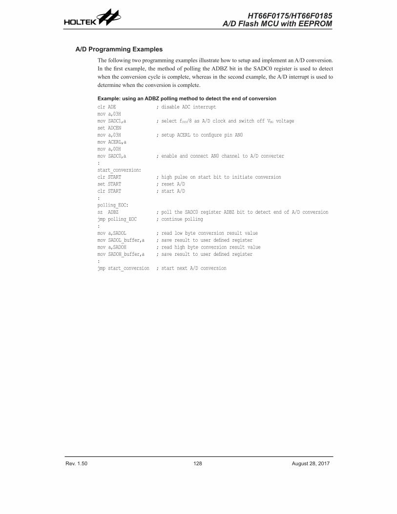
Rev. 1.50 1�� ����st ��� �01� Rev. 1.50 1�9 ����st ��� �01�
HT66F0175/HT66F0185A/D Flash MCU with EEPROM
HT66F0175/HT66F0185A/D Flash MCU with EEPROM
A/D Programming ExamplesThefollowingtwoprogrammingexamplesillustratehowtosetupandimplementanA/Dconversion.Inthefirstexample, themethodofpollingtheADBZbit intheSADC0registerisusedtodetectwhentheconversioncycleiscomplete,whereasinthesecondexample,theA/Dinterruptisusedtodeterminewhentheconversioniscomplete.
Example: using an ADBZ polling method to detect the end of conversionclr ADE ; disable ADC interruptmov a,03Hmov SADC1,a ; select fSYS/8 as A/D clock and switch off VBG voltageset ADCENmov a,03H ; setup ACERL to configure pin AN0mov ACERL,amov a,00Hmov SADC0,a ; enable and connect AN0 channel to A/D converter:start_conversion:clr START ; high pulse on start bit to initiate conversionset START ; reset A/Dclr START ; start A/D:polling_EOC:sz ADBZ ; poll the SADC0 register ADBZ bit to detect end of A/D conversionjmp polling_EOC ; continue polling:mov a,SADOL ; read low byte conversion result valuemov SADOL_buffer,a ; save result to user defined registermov a,SADOH ; read high byte conversion result valuemov SADOH_buffer,a ; save result to user defined register:jmp start_conversion ; start next A/D conversion
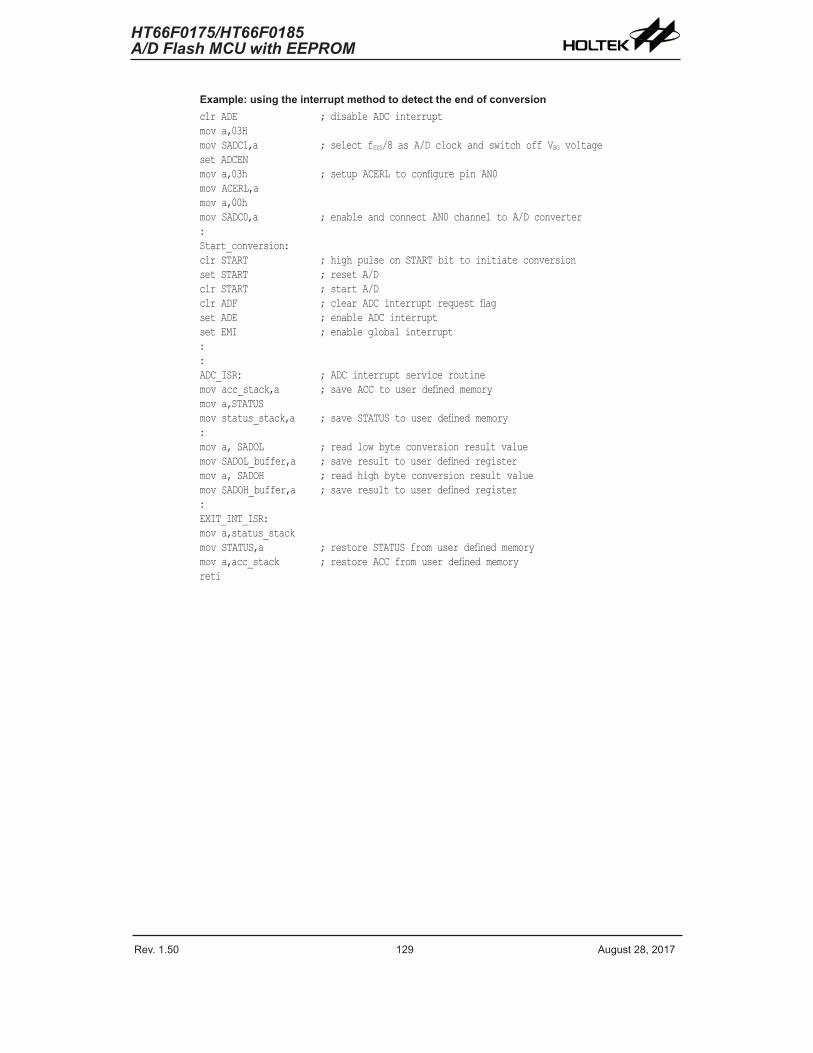
Rev. 1.50 1�� ����st ��� �01� Rev. 1.50 1�9 ����st ��� �01�
HT66F0175/HT66F0185A/D Flash MCU with EEPROM
HT66F0175/HT66F0185A/D Flash MCU with EEPROM
Example: using the interrupt method to detect the end of conversionclr ADE ; disable ADC interruptmov a,03Hmov SADC1,a ; select fSYS/8 as A/D clock and switch off VBG voltageset ADCENmov a,03h ; setup ACERL to configure pin AN0mov ACERL,amov a,00hmov SADC0,a ; enable and connect AN0 channel to A/D converter:Start_conversion:clr START ; high pulse on START bit to initiate conversionset START ; reset A/Dclr START ; start A/Dclr ADF ; clear ADC interrupt request flagset ADE ; enable ADC interruptset EMI ; enable global interrupt::ADC_ISR: ; ADC interrupt service routinemov acc_stack,a ; save ACC to user defined memorymov a,STATUSmov status_stack,a ; save STATUS to user defined memory:mov a, SADOL ; read low byte conversion result valuemov SADOL_buffer,a ; save result to user defined registermov a, SADOH ; read high byte conversion result valuemov SADOH_buffer,a ; save result to user defined register:EXIT_INT_ISR:mov a,status_stackmov STATUS,a ; restore STATUS from user defined memorymov a,acc_stack ; restore ACC from user defined memoryreti

Rev. 1.50 130 ����st ��� �01� Rev. 1.50 131 ����st ��� �01�
HT66F0175/HT66F0185A/D Flash MCU with EEPROM
HT66F0175/HT66F0185A/D Flash MCU with EEPROM
Serial Interface Module – SIMThesedevicescontainaSerialInterfaceModule,whichincludesboththefour-lineSPIinterfaceortwo-lineI2Cinterfacetypes, toallowaneasymethodofcommunicationwithexternalperipheralhardware.Havingrelativelysimplecommunicationprotocols, theseserial interface typesallowthemicrocontroller to interface toexternalSPIorI2Cbasedhardwaresuchassensors,FlashorEEPROMmemory,etc.TheSIMinterfacepinsarepin-sharedwithotherI/OpinsandthereforetheSIMinterfacefunctionalpinsmustfirstbeselectedusingthecorrespondingpin-sharedfunctionselectionbits.Asbothinterfacetypessharethesamepinsandregisters, thechoiceofwhethertheSPIorI2CtypeisusedismadeusingtheSIMoperatingmodecontrolbits,namedSIM2~SIM0,intheSIMC0register.Thesepull-highresistorsoftheSIMpin-sharedI/Opinsareselectedusingpull-highcontrolregisterswhentheSIMfunctionisenabledandthecorrespondingpinsareusedasSIMinputpins.
SPI InterfaceTheSPIinterfaceisoftenusedtocommunicatewithexternalperipheraldevicessuchassensors,FlashorEEPROMmemorydevices,etc.OriginallydevelopedbyMotorola, the four lineSPIinterfaceisasynchronousserialdatainterfacethathasarelativelysimplecommunicationprotocolsimplifyingtheprogrammingrequirementswhencommunicatingwithexternalhardwaredevices.
Thecommunicationisfullduplexandoperatesasaslave/mastertype,wherethedevicescanbeeithermasterorslave.AlthoughtheSPIinterfacespecificationcancontrolmultipleslavedevicesfromasinglemaster, thesedevicesprovidedonlyoneSCSpin. If themasterneeds tocontrolmultipleslavedevicesfromasinglemaster,themastercanuseI/Opintoselecttheslavedevices.
SPI Interface OperationTheSPIinterfaceisafullduplexsynchronousserialdatalink.It isafourlineinterfacewithpinnamesSDI,SDO,SCKandSCS.PinsSDIandSDOare theSerialData InputandSerialDataOutputlines,SCKistheSerialClocklineandSCSistheSlaveSelectline.AstheSPIinterfacepinsarepin-sharedwithnormalI/OpinsandwiththeI2Cfunctionpins,theSPIinterfacepinsmustfirstbeselectedbyconfiguringthepin-sharedfunctionselectionbitsandsettingthecorrectbitsintheSIMC0andSIMC2registers.AfterthedesiredSPIconfigurationhasbeensetitcanbedisabledorenabledusingtheSIMENbit in theSIMC0register.Communicationbetweendevicesconnectedto theSPI interface iscarriedout inaslave/mastermodewithalldata transfer initiationsbeingimplementedbythemaster.TheMasteralsocontrolstheclocksignal.AsthedevicesonlycontainasingleSCSpinonlyoneslavedevicecanbeutilized.TheSCSpiniscontrolledbysoftware,setCSENbitto1toenableSCSpinfunction,setCSENbitto0theSCSpinwillbefloatingstate.
TheSPIfunctioninthesedevicesofferthefollowingfeatures:
• Fullduplexsynchronousdatatransfer
• BothMasterandSlavemodes
• LSBfirstorMSBfirstdatatransmissionmodes
• Transmissioncompleteflag
• Risingorfallingactiveclockedge
ThestatusoftheSPIinterfacepinsisdeterminedbyanumberoffactorssuchaswhetherthedevicesareinthemasterorslavemodeandupontheconditionofcertaincontrolbitssuchasCSENandSIMEN.

Rev. 1.50 130 ����st ��� �01� Rev. 1.50 131 ����st ��� �01�
HT66F0175/HT66F0185A/D Flash MCU with EEPROM
HT66F0175/HT66F0185A/D Flash MCU with EEPROM
� � � � � � � � � � � � � � � � � � �
� � �
� � �
� � �
� � �
� � �
� � �
� � �
� � �
SPI Master/Slave Connection
� � � � � � � �
� � � � � � �
� � � � � � �
� � � �
� � � � � � � � � � � � � � � � �
� � � �� � � � � �
� � � � � � �
� � � � � � � �
� � � � �� � � � � � � � � � �
� � � � � �
� � � � �� � � � � � � � � � � �
� � � �� � � �
� � � � � � � � � � � � � � � � � � � � � �
� � � � � � �
� � � � � � �
� � � � � � � �
� � � � � � � �� � � � � � � � � �
SPI Block Diagram
SPI RegistersTherearethreeinternalregisterswhichcontroltheoveralloperationoftheSPIinterface.ThesearetheSIMDdataregisterandtworegistersSIMC0andSIMC2.NotethattheSIMC1registerisonlyusedbytheI2Cinterface.
Register Name
Bit
7 6 5 4 3 2 1 0SIMC0 SIM� SIM1 SIM0 — SIMDEB1 SIMDEB0 SIMEN SIMICFSIMC� D� D6 CKPOLB CKEG MLS CSEN WCOL TRFSIMD D� D6 D5 D4 D3 D� D1 D0
SPI Registers List
SIMD RegisterTheSIMDregisterisusedtostorethedatabeingtransmittedandreceived.ThesameregisterisusedbyboththeSPIandI2Cfunctions.BeforethedeviceswritedatatotheSPIbus,theactualdatatobetransmittedmustbeplacedintheSIMDregister.AfterthedataisreceivedfromtheSPIbus,thedevicecanreaditfromtheSIMDregister.AnytransmissionorreceptionofdatafromtheSPIbusmustbemadeviatheSIMDregister.
Bit 7 6 5 4 3 2 1 0Name D� D6 D5 D4 D3 D� D1 D0R/W R/W R/W R/W R/W R/W R/W R/W R/WPOR x x x x x x x x
“x”: �nknown

Rev. 1.50 13� ����st ��� �01� Rev. 1.50 133 ����st ��� �01�
HT66F0175/HT66F0185A/D Flash MCU with EEPROM
HT66F0175/HT66F0185A/D Flash MCU with EEPROM
TherearealsotwocontrolregistersfortheSPIinterface,SIMC0andSIMC2.NotethattheSIMC2registeralsohasthenameSIMAwhichisusedbytheI2Cfunction.TheSIMC1registerisnotusedbytheSPIfunction,onlybytheI2Cfunction.RegisterSIMC0isusedtocontroltheenable/disablefunctionandtosetthedatatransmissionclockfrequency.RegisterSIMC2isusedforothercontrolfunctionssuchasLSB/MSBselection,writecollisionflag,etc.
SIMC0 Register
Bit 7 6 5 4 3 2 1 0Name SIM� SIM1 SIM0 — SIMDEB1 SIMDEB0 SIMEN SIMICFR/W R/W R/W R/W — R/W R/W R/W R/WPOR 1 1 1 — 0 0 0 0
Bit7~5 SIM2~SIM0:SIMOperatingModeControl000:SPImastermode;SPIclockisfSYS/4001:SPImastermode;SPIclockisfSYS/16010:SPImastermode;SPIclockisfSYS/64011:SPImastermode;SPIclockisfTBC100:SPImastermode;SPIclockisTM1CCRPmatchfrequency/2101:SPIslavemode110:I2Cslavemode111:NonSIMfunction
ThesebitssetuptheoveralloperatingmodeoftheSIMfunction.AswellasselectingiftheI2CorSPIfunction,theyareusedtocontroltheSPIMaster/SlaveselectionandtheSPIMasterclockfrequency.TheSPIclockisafunctionofthesystemclockbutcanalsobechosentobesourcedfromTM1.IftheSPISlaveModeisselectedthentheclockwillbesuppliedbyanexternalMasterdevice.
Bit4 Unimplemented,readas“0”Bit3~2 SIMDEB1~SIMDEB0:I2CDebounceTimeSelection
00:Nodebounce01:2systemclockdebounce1x:4systemclockdebounce
Bit1 SIMEN:SIMEnableControl0:Disable1:Enable
Thebit is theoverallon/offcontrolfor theSIMinterface.WhentheSIMENbit isclearedtozerotodisabletheSIMinterface,theSDI,SDO,SCKandSCS,orSDAandSCLlineswill losetheirSPIorI2CfunctionandtheSIMoperatingcurrentwillbereducedtoaminimumvalue.WhenthebitishightheSIMinterfaceisenabled.IftheSIMisconfiguredtooperateasanSPIinterfaceviatheSIM2~SIM0bits,thecontentsoftheSPIcontrolregisterswillremainattheprevioussettingswhentheSIMENbitchangesfromlowtohighandshouldthereforebefirst initialisedbytheapplicationprogram.IftheSIMisconfiguredtooperateasanI2CinterfaceviatheSIM2~SIM0bitsandtheSIMENbitchangesfromlowtohigh,thecontentsoftheI2CcontrolbitssuchasHTXandTXAKwillremainattheprevioussettingsandshouldthereforebefirstinitialisedbytheapplicationprogramwhiletherelevantI2CflagssuchasHCF,HAAS,HBB,SRWandRXAKwillbesettotheirdefaultstates.
Bit0 SIMICF:SIMIncompleteFlag0:SIMincompleteconditionnotoccurred1:SIMincompleteconditionoccured
ThisbitisonlyavailablewhentheSIMisconfiguredtooperateinanSPIslavemode.IftheSPIoperatesintheslavemodewiththeSIMENandCSENbitsbothbeingsetto1buttheSCSlineispulledhighbytheexternalmasterdevicebeforetheSPIdatatransferiscompletelyfinished,theSIMICFbitwillbesetto1togetherwiththeTRFbit.Whenthisconditionoccurs,thecorrespondinginterruptwilloccuriftheinterruptfunctionisenabled.However,theTRFbitwillnotbesetto1iftheSIMICFbitissetto1bysoftwareapplicationprogram.

Rev. 1.50 13� ����st ��� �01� Rev. 1.50 133 ����st ��� �01�
HT66F0175/HT66F0185A/D Flash MCU with EEPROM
HT66F0175/HT66F0185A/D Flash MCU with EEPROM
SIMC2 Register
Bit 7 6 5 4 3 2 1 0Name D� D6 CKPOLB CKEG MLS CSEN WCOL TRFR/W R/W R/W R/W R/W R/W R/W R/W R/WPOR 0 0 0 0 0 0 0 0
Bit7~6 UndefinedbitsThesebitscanbereadorwrittenbytheapplicationprogram.
Bit5 CKPOLB:SPIclocklinebaseconditionselection0:TheSCKlinewillbehighwhentheclockisinactive.1:TheSCKlinewillbelowwhentheclockisinactive.
TheCKPOLBbitdeterminesthebaseconditionoftheclockline, if thebit ishigh,thentheSCKlinewillbelowwhentheclockisinactive.WhentheCKPOLBbitislow,thentheSCKlinewillbehighwhentheclockisinactive.
Bit4 CKEG:SPISCKclockactiveedgetypeselectionCKPOLB=00:SCKishighbaselevelanddatacaptureatSCKrisingedge1:SCKishighbaselevelanddatacaptureatSCKfallingedge
CKPOLB=10:SCKislowbaselevelanddatacaptureatSCKfallingedge1:SCKislowbaselevelanddatacaptureatSCKrisingedge
TheCKEGandCKPOLBbitsareusedtosetupthewaythattheclocksignaloutputsandinputsdataontheSPIbus.Thesetwobitsmustbeconfiguredbeforedatatransferisexecutedotherwiseanerroneousclockedgemaybegenerated.TheCKPOLBbitdeterminesthebaseconditionoftheclockline, if thebit ishigh,thentheSCKlinewillbelowwhentheclockisinactive.WhentheCKPOLBbitislow,thentheSCKlinewillbehighwhentheclockis inactive.TheCKEGbitdeterminesactiveclockedgetypewhichdependsupontheconditionofCKPOLBbit.
Bit3 MLS:SPIdatashiftorder0:LSBfirst1:MSBfirst
Thisisthedatashiftselectbitandisusedtoselecthowthedataistransferred,eitherMSBorLSBfirst.SettingthebithighwillselectMSBfirstandlowforLSBfirst.
Bit2 CSEN:SPISCSpincontrol0:Disable1:Enable
TheCSENbitisusedasanenable/disablefortheSCSpin.Ifthisbitislow,thentheSCSpinwillbedisabledandplacedintoafloatingcondition.Ifthebitishigh,theSCSpinwillbeenabledandusedasaselectpin.
Bit1 WCOL:SPIwritecollisionflag0:Nocollision1:Collision
TheWCOLflagisusedtodetectwhetheradatacollisionhasoccurredornot.Ifthisbit ishigh,itmeansthatdatahasbeenattemptedtobewrittentotheSIMDregisterdutingadatatransferoperation.Thiswritingoperationwillbeignoredifdataisbeingtransferred.Thisbitcanbeclearedbytheapplicationprogram.
Bit0 TRF:SPITransmit/Receivecompleteflag0:SPIdataisbeingtransferred1:SPIdatatransferiscompleted
TheTRFbitistheTransmit/ReceiveCompleteflagandissetto1automaticallywhenanSPIdatatransferiscompleted,butmustclearedto0bytheapplicationprogram.Itcanbeusedtogenerateaninterrupt.
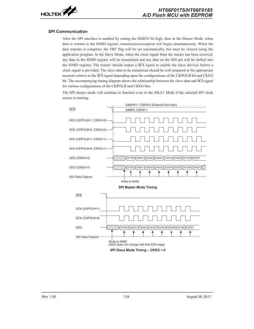
Rev. 1.50 134 ����st ��� �01� Rev. 1.50 135 ����st ��� �01�
HT66F0175/HT66F0185A/D Flash MCU with EEPROM
HT66F0175/HT66F0185A/D Flash MCU with EEPROM
SPI CommunicationAftertheSPIinterfaceisenabledbysettingtheSIMENbithigh,thenintheMasterMode,whendataiswrittentotheSIMDregister, transmission/receptionwillbeginsimultaneously.Whenthedata transfer iscomplete, theTRFflagwillbesetautomatically,butmustbeclearedusing theapplicationprogram.IntheSlaveMode,whentheclocksignalfromthemasterhasbeenreceived,anydataintheSIMDregisterwillbetransmittedandanydataontheSDIpinwillbeshiftedintotheSIMDregister.ThemastershouldoutputaSCSsignal toenable theslavedevicesbeforeaclocksignalisprovided.TheslavedatatobetransferredshouldbewellpreparedattheappropriatemomentrelativetotheSCSsignaldependingupontheconfigurationsoftheCKPOLBbitandCKEGbit.TheaccompanyingtimingdiagramshowstherelationshipbetweentheslavedataandSCSsignalforvariousconfigurationsoftheCKPOLBandCKEGbits.
TheSPImastermodewillcontinuetofunctionevenintheIDLE1ModeiftheselectedSPIclocksourceisrunning.
� � � � � � � � � � � � � � � � � � � � � �
� � � � � � � � � � �� � � � � � � � � � � � � � � � � � � � � � � � � � � � � � � �
� � � � � � � � � � � � � � � � � � � � � �
� � � � � � � � � � � � � � � � � � � � � �
� � � � � � � � � � � � � � � � � � � � � �
� � � � � � � � � � � �
� � � � � � � � � � � �
� � �
� � � � � � � � � � � � � �
� � � � � � � � � � � � � � � � � � � � � � � � � � � � � � � � � � � �
� � � � � � � � � � � � � � � � � � � � � � � � � � � � � � � � � � � �
� � � � � � � � � � �
SPI Master Mode Timing
� � � � � � � � � � � � � �
� � � � � � � � � � � � � �
� � �
� � �
� � � � � � � � � � � � � � �
� � � � � � � � � � � � � � � � � � � � � � � � � � � � � �
� � � � � � � � � � � � �� � � � � � � � � � � � � � � � � � � � � � � � � � � � � � � � � � � � � �
SPI Slave Mode Timing – CKEG = 0

Rev. 1.50 134 ����st ��� �01� Rev. 1.50 135 ����st ��� �01�
HT66F0175/HT66F0185A/D Flash MCU with EEPROM
HT66F0175/HT66F0185A/D Flash MCU with EEPROM
� � � � � � � � � � � � � �
� � � � � � � � � � � � � �
� � �
� � �
� � � � � � � � � � � � � � �
� � � � � � � � � � � � � � � � � � � � � � � � � � � � � �
� � � � � � � � � � � � �� � � � � � � � � � � � � � � � � � � � � � � � � � � � � � � � � � � � � � � � � � � � � � � � � � � � � � � � � � � � � �
� � � � � � � � � � � � � � � � � � � � � � � � � � � � � � � � � � � � � � � � � � � � � � � � � � � � � � � � � � � � � � � � � � � �� � � � � � � � � � � � � � � � � � � � � � � � � �
SPI Slave Mode Timing – CKEG = 1
� � � � � � � �
� � � � � � � � � �� � � � � � � � �
� � � � � �
� � � � � � � �
� � � � � � � � � � � �� � � � � � � � � �� � � � � � � � � �
�
� � � � � � � � �� � � � � � � � �
� � � � � � � �
� � � � � � � �� � � � � � � � �
�
� � �
� � � � � � � � �� � � ��
� � � � � � � � � �
�
�
� � � � � � � � � � � �
� � � � � � � � � � � � � �� � � � � � � � � � � � � � � � � � �
� � � � � � � � � � � � �� � � � � � � � � � � � � � � � � � � � � � � � � � � � � � � �
SPI Transfer Control Flow Chart

Rev. 1.50 136 ����st ��� �01� Rev. 1.50 13� ����st ��� �01�
HT66F0175/HT66F0185A/D Flash MCU with EEPROM
HT66F0175/HT66F0185A/D Flash MCU with EEPROM
I2C InterfaceThe I2C interface isused to communicatewith externalperipheraldevices suchas sensors,EEPROMmemoryetc.OriginallydevelopedbyPhilips,it isatwolinelowspeedserialinterfaceforsynchronousserialdatatransfer.Theadvantageofonlytwolinesforcommunication,relativelysimplecommunicationprotocolandtheabilitytoaccommodatemultipledevicesonthesamebushasmadeitanextremelypopularinterfacetypeformanyapplications.
� � � � � �� � � � �
� � � � � �� � � � � �
� � � � � �� � � � �
� � �
� � �� � �
I2C Master Slave Bus Connection
I2C interface OperationTheI2Cserialinterfaceisatwolineinterface,aserialdataline,SDA,andserialclockline,SCL.Asmanydevicesmaybeconnectedtogetheronthesamebus,theiroutputsarebothopendraintypes.Forthisreasonitisnecessarythatexternalpull-highresistorsareconnectedtotheseoutputs.Notethatnochipselectlineexists,aseachdeviceontheI2CbusisidentifiedbyauniqueaddresswhichwillbetransmittedandreceivedontheI2Cbus.
WhentwodevicescommunicatewitheachotheronthebidirectionalI2Cbus,oneisknownasthemasterdeviceandoneas theslavedevice.Bothmasterandslavecantransmitandreceivedata,however, it isthemasterdevicethathasoverallcontrolofthebus.Forthesedevices,whichonlyoperateinslavemode,therearetwomethodsoftransferringdataontheI2Cbus,theslavetransmitmodeandtheslavereceivemode.
� � � � � � � � � � � � � � � � �� � � � � �
� � � � � � � � � � � � � � � � � � � � �� � � � � �
� � � � � � � � � � � �
� � � � � � � � � � � � � � � � �
���
� � � � � � � � � � � � � � � � � � � � � � � � � � � � � � � � �
� � � � � � � � � � � �� � � � � � � � � � � � �
� � � � � � � � � � � � � � �� � � � � � � � � � � �
� � � � � � � � � � � � � � � � �
� � � � � � � � � � � � � � � � � � � �
� � � � � � � �
� � � � � � �� � � � � � � � � �
� � � �
� � � � � � � � � � � � � � � � � � � � � �
� � � � � � �
� � � � � � �
� � � � � � �
� � � � � � �� � � � � � � � �
� � � � � � �� � � � � � �
� � �
� � � � � � ��
� � � � � � �
� � � � � � � � �
� � � � � � �� � � � � � � � � � � � �
� � � � � � � � � � � �
� � � � � � � � � �
I2C Block Diagram

Rev. 1.50 136 ����st ��� �01� Rev. 1.50 13� ����st ��� �01�
HT66F0175/HT66F0185A/D Flash MCU with EEPROM
HT66F0175/HT66F0185A/D Flash MCU with EEPROM
� � � � � � � � � � � �� � � � � � � � � � �
� � � � � � � � � � � � � � �� � � � � � � � � � � � � � � � � � � �
� � � � � � � � � �� � � � � � � � � �
� � � � � � � � � � �� � � � � � � � � � �
� � � � � � � � � �� � � � � � � � � �
� � � � � � � � � � �� � � � � � � � � � �
TheSIMDEB1andSIMDEB0bitsdetermine thedebounce timeof theI2Cinterface.Thisusesthesystemclockto ineffectaddadebouncetimeto theexternalclocktoreducethepossibilityofglitchesontheclocklinecausingerroneousoperation.Thedebouncetime, ifselected,canbechosen tobeeither2or4systemclocks.Toachieve therequiredI2Cdata transferspeed, thereexistsarelationshipbetweenthesystemclock,fSYS,andtheI2Cdebouncetime.ForeithertheI2CStandardorFastmodeoperation,usersmusttakecareoftheselectedsystemclockfrequencyandtheconfigureddebouncetimetomatchthecriterionshowninthefollowingtable.
I2C Debounce Time Selection I2C Standard Mode (100kHz) I2C Fast Mode (400kHz)No Devo�nce fSYS > � MHz fSYS > 5 MHz� system clock debo�nce fSYS > 4 MHz fSYS > 10 MHz4 system clock debo�nce fSYS > � MHz fSYS > �0 MHz
I2C Minimum fSYS Frequency
I2C RegistersThereare threecontrolregistersassociatedwiththeI2Cbus,SIMC0,SIMC1andSIMTOC,oneslaveaddressregister,SIMA,andonedataregister,SIMD.TheSIMDregister,whichisshownintheaboveSPIsection,isusedtostorethedatabeingtransmittedandreceivedontheI2Cbus.BeforethemicrocontrollerwritesdatatotheI2Cbus,theactualdatatobetransmittedmustbeplacedintheSIMDregister.AfterthedataisreceivedfromtheI2Cbus,themicrocontrollercanreaditfromtheSIMDregister.AnytransmissionorreceptionofdatafromtheI2CbusmustbemadeviatheSIMDregister.
NotethattheSIMAregisteralsohasthenameSIMC2whichisusedbytheSPIfunction.BitSIMENandbitsSIM2~SIM0inregisterSIMC0areusedbytheI2Cinterface.
Register Name
Bit
7 6 5 4 3 2 1 0SIMC0 SIM� SIM1 SIM0 — SIMDEB1 SIMDEB0 SIMEN SIMICFSIMC1 HCF H��S HBB HTX TX�K SRW I�MWU RX�KSIM� IIC�6 IIC�5 IIC�4 IIC�3 IIC�� IIC�1 IIC�0 D0SIMD D� D6 D5 D4 D3 D� D1 D0
SIMTOC SIMTOEN SIMTOF SIMTOS5 SIMTOS4 SIMTOS3 SIMTOS� SIMTOS1 SIMTOS0
I2C Registers List

Rev. 1.50 13� ����st ��� �01� Rev. 1.50 139 ����st ��� �01�
HT66F0175/HT66F0185A/D Flash MCU with EEPROM
HT66F0175/HT66F0185A/D Flash MCU with EEPROM
SIMD RegisterTheSIMDregisterisusedtostorethedatabeingtransmittedandreceived.ThesameregisterisusedbyboththeSPIandI2Cfunctions.BeforethedevicewritesdatatotheI2Cbus,theactualdatatobetransmittedmustbeplacedintheSIMDregister.AfterthedataisreceivedfromtheI2Cbus,thedevicecanreaditfromtheSIMDregister.AnytransmissionorreceptionofdatafromtheI2CbusmustbemadeviatheSIMDregister.
Bit 7 6 5 4 3 2 1 0Name D� D6 D5 D4 D3 D� D1 D0R/W R/W R/W R/W R/W R/W R/W R/W R/WPOR x x x x x x x x
“x”: �nknown
SIMA RegisterTheSIMAregisterisalsousedbytheSPIinterfacebuthasthenameSIMC2.TheSIMAregisteristhelocationwherethe7-bitslaveaddressoftheslavedeviceisstored.Bits7~1oftheSIMAregisterdefinethedeviceslaveaddress.Bit0isnotdefined.
Whenamasterdevice,whichisconnectedtotheI2Cbus,sendsoutanaddress,whichmatchestheslaveaddressintheSIMAregister,theslavedevicewillbeselected.NotethattheSIMAregisteristhesameregisteraddressasSIMC2whichisusedbytheSPIinterface.
Bit 7 6 5 4 3 2 1 0Name IIC�6 IIC�5 IIC�4 IIC�3 IIC�� IIC�1 IIC�0 D0R/W R/W R/W R/W R/W R/W R/W R/W R/WPOR x x x x x x x x
“x”: �nknownBit7~1 IICA6~IICA0:I2Cslaveaddress
IICA6~IICA0istheI2Cslaveaddressbit6~bit0Bit0 Undefinedbit
Thebitcanbereadorwrittenbytheapplicationprogram.Therearealso threecontrol registers for the I2Cinterface,SIMC0,SIMC1andSIMTOC.TheregisterSIMC0isused tocontrol theenable/disable functionand toset thedata transmissionclockfrequency.TheSIMC1registercontainstherelevantflagswhichareusedtoindicatetheI2Ccommunicationstatus.TheSIMTOCregisterisusedtocontroltheI2Cbustime-outfunctionwhichisdescribedintheI2CTime-outControlsection.
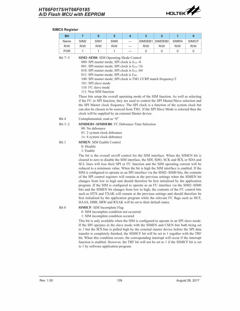
Rev. 1.50 13� ����st ��� �01� Rev. 1.50 139 ����st ��� �01�
HT66F0175/HT66F0185A/D Flash MCU with EEPROM
HT66F0175/HT66F0185A/D Flash MCU with EEPROM
SIMC0 Register
Bit 7 6 5 4 3 2 1 0Name SIM� SIM1 SIM0 — SIMDEB1 SIMDEB0 SIMEN SIMICFR/W R/W R/W R/W — R/W R/W R/W R/WPOR 1 1 1 — 0 0 0 0
Bit7~5 SIM2~SIM0:SIMOperatingModeControl000:SPImastermode;SPIclockisfSYS/4001:SPImastermode;SPIclockisfSYS/16010:SPImastermode;SPIclockisfSYS/64011:SPImastermode;SPIclockisfTBC100:SPImastermode;SPIclockisTM1CCRPmatchfrequency/2101:SPIslavemode110:I2Cslavemode111:NonSIMfunction
ThesebitssetuptheoveralloperatingmodeoftheSIMfunction.AswellasselectingiftheI2CorSPIfunction,theyareusedtocontroltheSPIMaster/SlaveselectionandtheSPIMasterclockfrequency.TheSPIclockisafunctionofthesystemclockbutcanalsobechosentobesourcedfromTM1.IftheSPISlaveModeisselectedthentheclockwillbesuppliedbyanexternalMasterdevice.
Bit4 Unimplemented,readas“0”Bit3~2 SIMDEB1~SIMDEB0:I2CDebounceTimeSelection
00:Nodebounce01:2systemclockdebounce1x:4systemclockdebounce
Bit1 SIMEN:SIMEnableControl0:Disable1:Enable
Thebit is theoverallon/offcontrolfor theSIMinterface.WhentheSIMENbit isclearedtozerotodisabletheSIMinterface,theSDI,SDO,SCKandSCS,orSDAandSCLlineswill losetheirSPIorI2CfunctionandtheSIMoperatingcurrentwillbereducedtoaminimumvalue.WhenthebitishightheSIMinterfaceisenabled.IftheSIMisconfiguredtooperateasanSPIinterfaceviatheSIM2~SIM0bits,thecontentsoftheSPIcontrolregisterswillremainattheprevioussettingswhentheSIMENbitchangesfromlowtohighandshouldthereforebefirst initialisedbytheapplicationprogram.IftheSIMisconfiguredtooperateasanI2CinterfaceviatheSIM2~SIM0bitsandtheSIMENbitchangesfromlowtohigh,thecontentsoftheI2CcontrolbitssuchasHTXandTXAKwillremainattheprevioussettingsandshouldthereforebefirstinitialisedbytheapplicationprogramwhiletherelevantI2CflagssuchasHCF,HAAS,HBB,SRWandRXAKwillbesettotheirdefaultstates.
Bit0 SIMICF:SIMIncompleteFlag0:SIMincompleteconditionnotoccurred1:SIMincompleteconditionoccured
ThisbitisonlyavailablewhentheSIMisconfiguredtooperateinanSPIslavemode.IftheSPIoperatesintheslavemodewiththeSIMENandCSENbitsbothbeingsetto1buttheSCSlineispulledhighbytheexternalmasterdevicebeforetheSPIdatatransferiscompletelyfinished,theSIMICFbitwillbesetto1togetherwiththeTRFbit.Whenthisconditionoccurs,thecorrespondinginterruptwilloccuriftheinterruptfunctionisenabled.However,theTRFbitwillnotbesetto1iftheSIMICFbitissetto1bysoftwareapplicationprogram.
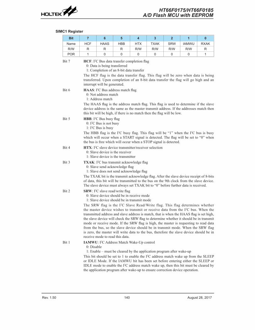
Rev. 1.50 140 ����st ��� �01� Rev. 1.50 141 ����st ��� �01�
HT66F0175/HT66F0185A/D Flash MCU with EEPROM
HT66F0175/HT66F0185A/D Flash MCU with EEPROM
SIMC1 Register
Bit 7 6 5 4 3 2 1 0Name HCF H��S HBB HTX TX�K SRW I�MWU RX�KR/W R R R R/W R/W R/W R/W RPOR 1 0 0 0 0 0 0 1
Bit7 HCF:I2CBusdatatransfercompletionflag0:Dataisbeingtransferred1:Completionofan8-bitdatatransfer
TheHCFflag is thedata transfer flag.This flagwillbezerowhendata isbeingtransferred.Uponcompletionofan8-bitdata transfer theflagwillgohighandaninterruptwillbegenerated.
Bit6 HAAS:I2CBusaddressmatchflag0:Notaddressmatch1:Addressmatch
TheHAASflagistheaddressmatchflag.Thisflagisusedtodetermineiftheslavedeviceaddressisthesameasthemastertransmitaddress.Iftheaddressesmatchthenthisbitwillbehigh,ifthereisnomatchthentheflagwillbelow.
Bit5 HBB:I2CBusbusyflag0:I2CBusisnotbusy1:I2CBusisbusy
TheHBBflagis theI2Cbusyflag.Thisflagwillbe“1”whentheI2CbusisbusywhichwilloccurwhenaSTARTsignalisdetected.Theflagwillbesetto“0”whenthebusisfreewhichwilloccurwhenaSTOPsignalisdetected.
Bit4 HTX:I2Cslavedevicetransmitter/receiverselection0:Slavedeviceisthereceiver1:Slavedeviceisthetransmitter
Bit3 TXAK:I2Cbustransmitacknowledgeflag0:Slavesendacknowledgeflag1:Slavedoesnotsendacknowledgeflag
TheTXAKbitisthetransmitacknowledgeflag.Aftertheslavedevicereceiptof8-bitsofdata,thisbitwillbetransmittedtothebusonthe9thclockfromtheslavedevice.TheslavedevicemustalwayssetTXAKbitto“0”beforefurtherdataisreceived.
Bit2 SRW:I2Cslaveread/writeflag0:Slavedeviceshouldbeinreceivemode1:Slavedeviceshouldbeintransmitmode
TheSRWflag is the I2CSlaveRead/Write flag.This flagdetermineswhetherthemasterdevicewishes to transmitor receivedata fromthe I2Cbus.When thetransmittedaddressandslaveaddressismatch,thatiswhentheHAASflagissethigh,theslavedevicewillchecktheSRWflagtodeterminewhetheritshouldbeintransmitmodeorreceivemode.IftheSRWflagishigh,themasterisrequestingtoreaddatafromthebus,so theslavedeviceshouldbe in transmitmode.WhentheSRWflagiszero,themasterwillwritedatatothebus,thereforetheslavedeviceshouldbeinreceivemodetoreadthisdata.
Bit1 IAMWU:I2CAddressMatchWake-Upcontrol0:Disable1:Enable–mustbeclearedbytheapplicationprogramafterwake-up
Thisbitshouldbesetto1toenabletheI2CaddressmatchwakeupfromtheSLEEPorIDLEMode.IftheIAMWUbithasbeensetbeforeenteringeithertheSLEEPorIDLEmodetoenabletheI2Caddressmatchwakeup,thenthisbitmustbeclearedbytheapplicationprogramafterwake-uptoensurecorrectiondeviceoperation.
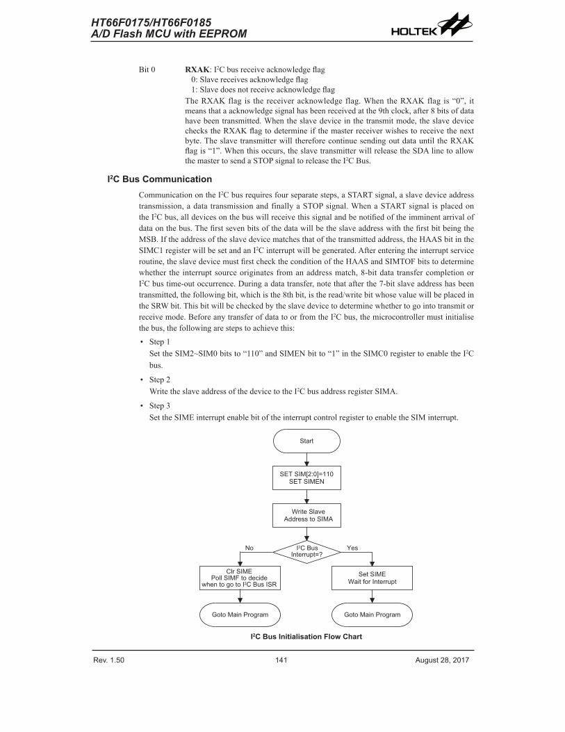
Rev. 1.50 140 ����st ��� �01� Rev. 1.50 141 ����st ��� �01�
HT66F0175/HT66F0185A/D Flash MCU with EEPROM
HT66F0175/HT66F0185A/D Flash MCU with EEPROM
Bit0 RXAK:I2Cbusreceiveacknowledgeflag0:Slavereceivesacknowledgeflag1:Slavedoesnotreceiveacknowledgeflag
TheRXAKflag is thereceiveracknowledgeflag.WhentheRXAKflag is“0”, itmeansthataacknowledgesignalhasbeenreceivedatthe9thclock,after8bitsofdatahavebeentransmitted.Whentheslavedeviceinthetransmitmode,theslavedevicecheckstheRXAKflagtodetermineifthemasterreceiverwishestoreceivethenextbyte.Theslavetransmitterwill thereforecontinuesendingoutdatauntil theRXAKflagis“1”.Whenthisoccurs,theslavetransmitterwillreleasetheSDAlinetoallowthemastertosendaSTOPsignaltoreleasetheI2CBus.
I2C Bus CommunicationCommunicationontheI2Cbusrequiresfourseparatesteps,aSTARTsignal,aslavedeviceaddresstransmission,adatatransmissionandfinallyaSTOPsignal.WhenaSTARTsignal isplacedontheI2Cbus,alldevicesonthebuswillreceivethissignalandbenotifiedoftheimminentarrivalofdataonthebus.ThefirstsevenbitsofthedatawillbetheslaveaddresswiththefirstbitbeingtheMSB.Iftheaddressoftheslavedevicematchesthatofthetransmittedaddress,theHAASbitintheSIMC1registerwillbesetandanI2Cinterruptwillbegenerated.Afterenteringtheinterruptserviceroutine,theslavedevicemustfirstchecktheconditionoftheHAASandSIMTOFbitstodeterminewhether the interruptsourceoriginatesfromanaddressmatch,8-bitdata transfercompletionorI2Cbustime-outoccurrence.Duringadatatransfer,notethatafterthe7-bitslaveaddresshasbeentransmitted,thefollowingbit,whichisthe8thbit,istheread/writebitwhosevaluewillbeplacedintheSRWbit.Thisbitwillbecheckedbytheslavedevicetodeterminewhethertogointotransmitorreceivemode.BeforeanytransferofdatatoorfromtheI2Cbus,themicrocontrollermustinitialisethebus,thefollowingarestepstoachievethis:
• Step1SettheSIM2~SIM0bitsto“110”andSIMENbitto“1”intheSIMC0registertoenabletheI2Cbus.
• Step2WritetheslaveaddressofthedevicetotheI2CbusaddressregisterSIMA.
• Step3SettheSIMEinterruptenablebitoftheinterruptcontrolregistertoenabletheSIMinterrupt.
� � � � �
� � � � � � � � � � � � �� � � � � � � � � � � � � � � � �
� � � � � � � � � � � � � � � � � � � � �
� � � � � � � � � �� � � � � � � � � � �
�
� � �� �
� � � � � � � �� � � � � � � � � � � � � � � � � �
� � � � � � � � � � � � � � � �
� � � � � � � � �� � � � � � � � � � � � � � � � � � �
� � � � � � � � � � � � � � � � � � � � � � � � � �
� � � � � � � � � � � � � � � �
I2C Bus Initialisation Flow Chart

Rev. 1.50 14� ����st ��� �01� Rev. 1.50 143 ����st ��� �01�
HT66F0175/HT66F0185A/D Flash MCU with EEPROM
HT66F0175/HT66F0185A/D Flash MCU with EEPROM
I2C Bus Start SignalTheSTARTsignalcanonlybegeneratedbythemasterdeviceconnectedtotheI2Cbusandnotbytheslavedevice.ThisSTARTsignalwillbedetectedbyalldevicesconnectedtotheI2Cbus.Whendetected, this indicates that theI2Cbusisbusyandtherefore theHBBbitwillbeset.ASTARTconditionoccurswhenahigh to lowtransitionon theSDAline takesplacewhentheSCLlineremainshigh.
I2C Slave AddressThetransmissionofaSTARTsignalbythemasterwillbedetectedbyalldevicesontheI2Cbus.Todeterminewhichslavedevicethemasterwishestocommunicatewith,theaddressoftheslavedevicewillbesentoutimmediatelyfollowingtheSTARTsignal.Allslavedevices,afterreceivingthis7-bitaddressdata,willcompareitwiththeirown7-bitslaveaddress.Iftheaddresssentoutbythemastermatchestheinternaladdressofthemicrocontrollerslavedevice,thenaninternalI2Cbusinterruptsignalwillbegenerated.Thenextbitfollowingtheaddress,whichisthe8thbit,definestheread/writestatusandwillbesavedtotheSRWbitoftheSIMC1register.Theslavedevicewillthentransmitanacknowledgebit,whichisalowlevel,asthe9thbit.TheslavedevicewillalsosetthestatusflagHAASwhentheaddressesmatch.
Asan I2Cbus interruptcancome from three sources,when theprogramenters the interruptsubroutine,theHAASandSIMTOFbitsshouldbeexaminedtoseewhethertheinterruptsourcehascomefromamatchingslaveaddress,thecompletionofadatabytetransferortheI2Cbustime-outoccurrence.Whenaslaveaddressismatched,thedevicesmustbeplacedineitherthetransmitmodeandthenwritedatatotheSIMDregister,orinthereceivemodewhereitmustimplementadummyreadfromtheSIMDregistertoreleasetheSCLline.
I2C Bus Read/Write SignalTheSRWbitintheSIMC1registerdefineswhetherthemasterdevicewishestoreaddatafromtheI2CbusorwritedatatotheI2Cbus.Theslavedeviceshouldexaminethisbittodetermineifitistobeatransmitterorareceiver.IftheSRWflagis“1”thenthisindicatesthatthemasterdevicewishestoreaddatafromtheI2Cbus,thereforetheslavedevicemustbesetuptosenddatatotheI2Cbusasatransmitter.IftheSRWflagis“0”thenthisindicatesthatthemasterwishestosenddatatotheI2Cbus,thereforetheslavedevicemustbesetuptoreaddatafromtheI2Cbusasareceiver.
I2C Bus Slave Address Acknowledge SignalAfter themasterhas transmitted a calling address, any slavedeviceon the I2Cbus,whoseown internaladdressmatches thecallingaddress,mustgenerateanacknowledgesignal.Theacknowledgesignalwillinformthemasterthataslavedevicehasaccepteditscallingaddress.IfnoacknowledgesignalisreceivedbythemasterthenaSTOPsignalmustbetransmittedbythemastertoendthecommunication.WhentheHAASflagishigh,theaddresseshavematchedandtheslavedevicemustchecktheSRWflagtodetermineifitistobeatransmitterorareceiver.IftheSRWflagishigh,theslavedeviceshouldbesetuptobeatransmittersotheHTXbitintheSIMC1registershouldbesetto“1”.IftheSRWflagislow,thenthemicrocontrollerslavedeviceshouldbesetupasareceiverandtheHTXbitintheSIMC1registershouldbesetto“0”.
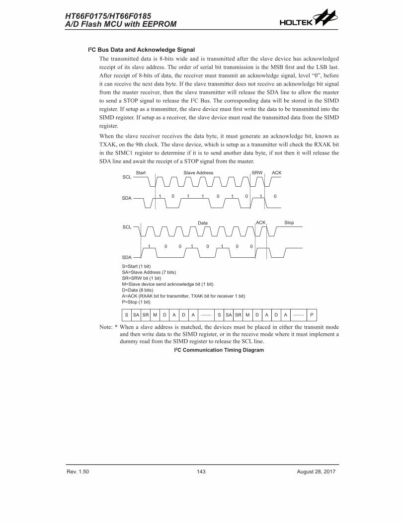
Rev. 1.50 14� ����st ��� �01� Rev. 1.50 143 ����st ��� �01�
HT66F0175/HT66F0185A/D Flash MCU with EEPROM
HT66F0175/HT66F0185A/D Flash MCU with EEPROM
I2C Bus Data and Acknowledge SignalThe transmitteddata is8-bitswideand is transmittedafter theslavedevicehasacknowledgedreceiptofitsslaveaddress.TheorderofserialbittransmissionistheMSBfirstandtheLSBlast.Afterreceiptof8-bitsofdata,thereceivermusttransmitanacknowledgesignal,level“0”,beforeitcanreceivethenextdatabyte.Iftheslavetransmitterdoesnotreceiveanacknowledgebitsignalfromthemasterreceiver, thentheslavetransmitterwillreleasetheSDAlinetoallowthemastertosendaSTOPsignaltoreleasetheI2CBus.ThecorrespondingdatawillbestoredintheSIMDregister.Ifsetupasatransmitter,theslavedevicemustfirstwritethedatatobetransmittedintotheSIMDregister.Ifsetupasareceiver,theslavedevicemustreadthetransmitteddatafromtheSIMDregister.
Whentheslavereceiver receives thedatabyte, itmustgenerateanacknowledgebit,knownasTXAK,onthe9thclock.Theslavedevice,whichissetupasatransmitterwillchecktheRXAKbitintheSIMC1registertodetermineifit istosendanotherdatabyte,ifnotthenitwillreleasetheSDAlineandawaitthereceiptofaSTOPsignalfromthemaster.
� � � �
� � � � � � � � � �� � � � � � � � � � ��
� � � � � � �� �
� � � � � � � � � � � � � � �� � � � � � � � � � � � � � � � � � � � � �� � � � � � � � � � � � � � � � � � � � � � � � � � � � � � � � � � � � � � � � � � � � � � � � � � � � � � � � � �� � � � � � � � � � � � � �� � � � � � � � � � � � � � � � � � � � � � � � � � � � � � � � � � � � � � � � � � � � � � � � � � � � � � � � � � � � � � � � � � � � � � � �
� � �� � � � �
� � �
� � � � �
� � � � � � � � �
� � �
� � � � � � � � � � �
� � � � � � � � � � � � � � � � � �
Note:*Whenaslaveaddressismatched,thedevicesmustbeplacedineitherthetransmitmodeandthenwritedatatotheSIMDregister,orinthereceivemodewhereitmustimplementadummyreadfromtheSIMDregistertoreleasetheSCLline.
I2C Communication Timing Diagram

Rev. 1.50 144 ����st ��� �01� Rev. 1.50 145 ����st ��� �01�
HT66F0175/HT66F0185A/D Flash MCU with EEPROM
HT66F0175/HT66F0185A/D Flash MCU with EEPROM
� � � � � ��
� � � � �� � � � �
� � � � �� � � � � �
� � �� �
� � � � �
� � � � � ��
� � �
� �
� �
� � � � � � � � � � � � � � � � � � � � �
� � � � � � � �
� � �
� � �
� � � � � � � � � � � � � � � � � � � � � � � � �
� � � � � � � �
� � �
� � �
� � � � � � � � � � � � � � � �� � � � � � � � � � � � � � � �
� � � � � � �
� � � � � � � � � � � � � � � �� � � � � � � � � � � � � � � � � � �
� � �
� � � � � � �� � � � � � � �
� � � � � � � � � � � � � � � � � � � � � � � � �
� � � � � � � �
� � � � � � �� � � � � � � �
� � �
� � � � �
� � � � � � ��
� � �� �
� � � � � � � � � �� � � � � � � � �
� � �
I2C Bus ISR Flow Chart
I2C Time-out ControlInordertoreducetheI2Clockupproblemduetoreceptionoferroneousclocksources,atime-outfunctionisprovided.IftheclocksourceconnectedtotheI2Cbusisnotreceivedforawhile,thentheI2Ccircuitryandregisterswillberesetafteracertaintime-outperiod.Thetime-outcounterstartstocountonanI2Cbus“START”&“addressmatch”condition,andisclearedbyanSCLfallingedge.Before thenextSCLfallingedgearrives, if the timeelapsedisgreater than the time-outperiodspecifiedbytheSIMTOCregister,thenatime-outconditionwilloccur.Thetime-outfunctionwillstopwhenanI2C“STOP”conditionoccurs.

Rev. 1.50 144 ����st ��� �01� Rev. 1.50 145 ����st ��� �01�
HT66F0175/HT66F0185A/D Flash MCU with EEPROM
HT66F0175/HT66F0185A/D Flash MCU with EEPROM
� � � � � � � � � � � �� � � � � � � � � � � � �
� � � � � � � � � � � � � � � � � � � � � � � � � �� � � � � � � � � � � � � � � � � � � � � � � � �
� � � � � � � � � �� � � � � � � � � � ��
� � � � � � �� �
� � �� � � � �
�
� � � � �
� � � �� � �
�
� � � � � � � � � � �
�
�
I2C Time-out
WhenanI2Ctime-outcounteroverflowoccurs, thecounterwillstopandtheSIMTOENbitwillbeclearedtozeroandtheSIMTOFbitwillbesethightoindicate thata time-outconditionhasoccurred.Thetime-outconditionwillalsogenerateaninterruptwhichusestheI2Cinterrruptvector.WhenanI2Ctime-outoccurs,theI2Cinternalcircuitrywillberesetandtheregisterswillberesetintothefollowingcondition:
Register After I2C Time-outSIMD� SIM�� SIMC0 No chan�eSIMC1 Reset to POR condition
I2C Register after Time-out
TheSIMTOFflagcanbeclearedbytheapplicationprogram.Thereare64time-outperiodselectionswhichcanbeselectedusingtheSIMTOSbits in theSIMTOCregister.Thetime-outduration iscalculatedbytheformula:((1~64)×(32/fSUB)).Thisgivesa time-outperiodwhichrangesfromabout1msto64ms.
SIMTOC Register
Bit 7 6 5 4 3 2 1 0Name SIMTOEN SIMTOF SIMTOS5 SIMTOS4 SIMTOS3 SIMTOS� SIMTOS1 SIMTOS0R/W R/W R/W R/W R/W R/W R/W R/W R/WPOR 0 0 0 0 0 0 0 0
Bit7 SIMTOEN:SIMI2CTime-outfunctioncontrol0:Disable1:Enable
Bit6 SIMTOF:SIMI2CTime-outflag0:Notime-outoccurred1:Time-outoccurred
Bit5~0 SIMTOS5~SIMTOS0:SIMI2CTime-outperiodselectionI2CTime-outclocksourceisfSUB/32
I2CTime-outperiodisequalto(SIMTOS[5:0]+1)× 32fSUB

Rev. 1.50 146 ����st ��� �01� Rev. 1.50 14� ����st ��� �01�
HT66F0175/HT66F0185A/D Flash MCU with EEPROM
HT66F0175/HT66F0185A/D Flash MCU with EEPROM
ComparatorsAnanalogcomparator iscontainedonlywithintheHT66F0185device.Thecomparatorfunctionoffersflexibilityviatheirregistercontrolledfeaturessuchaspower-down,polarityselect,hysteresisetc.InsharingtheirpinswithnormalI/OpinsthecomparatorsdonotwastepreciousI/Opinsiftherefunctionsareotherwiseunused.
� � �
� � �
� � � � � � � � � �
� � �
� � � � � � � � � � � � � � � �� � � � � � � � � �
Comparator
Comparator OperationTheHT66F0185devicecontainsacomparator functionwhich isused tocompare twoanalogvoltagesandprovideanoutputbasedontheirdifference.FullcontrolovertheinternalcomparatorisprovidedviathecontrolregisterCPCassignedtothecomparator.Thecomparatoroutputisrecordedviaabit in thecontrolregister,butcanalsobetransferredoutontoasharedI/Opin.Additionalcomparatorfunctionsincludeoutputpolarity,hysteresisfunctionsandpowerdowncontrol.
Anypull-high resistorsconnected to the sharedcomparator inputpinswillbeautomaticallydisconnectedwhenthecomparatorisenabled.Asthecomparatorinputsapproachtheirswitchinglevel,somespuriousoutputsignalsmaybegeneratedonthecomparatoroutputdueto theslowrisingor fallingnatureof the inputsignals.Thiscanbeminimisedbyselecting thehysteresisfunctionwhich applies a small amountofpositive feedback to the comparator. Ideally thecomparatorshouldswitchatthepointwherethepositiveandnegativeinputssignalsareatthesamevoltagelevel.However,unavoidableinputoffsetsintroducesomeuncertaintieshere.Thehysteresisfunction,ifenabled,alsoincreasestheswitchingoffsetvalue.
Comparator InterruptThecomparatorpossesses itsowninterruptfunction.Whenthecomparatoroutputchangesstate,itsrelevantinterruptflagwillbeset,andifthecorrespondinginterruptenablebitisset,thenajumptoitsrelevantinterruptvectorwillbeexecuted.NotethatitisthechangingstateoftheCOUTbitandnottheoutputpinwhichgeneratesaninterrupt.IfthemicrocontrollerisintheSLEEPorIDLEModeandtheComparatorisenabled,theniftheexternalinputlinescausetheComparatoroutputtochangestate,theresultinggeneratedinterruptflagwillalsogenerateawake-up.Ifitisrequiredtodisableawake-upfromoccurring,thentheinterruptflagshouldbefirstsethighbeforeenteringtheSLEEPorIDLEMode.
Programming ConsiderationsIf thecomparator isenabled, itwillremainactivewhenthemicrocontrollerenters theSLEEPorIDLEMode,howeverasitwillconsumeacertainamountofpower,theusermaywishtoconsiderdisablingitbeforetheSLEEPorIDLEModeisentered.AscomparatorpinsaresharedwithnormalI/Opins,theI/Oregistersforthesepinswillbereadaszero(portcontrolregisteris“1”)orreadasportdataregistervalue(portcontrolregisteris“0”)ifthecomparatorfunctionisenabled.
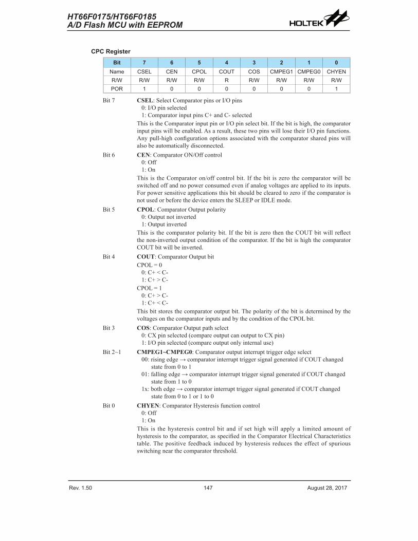
Rev. 1.50 146 ����st ��� �01� Rev. 1.50 14� ����st ��� �01�
HT66F0175/HT66F0185A/D Flash MCU with EEPROM
HT66F0175/HT66F0185A/D Flash MCU with EEPROM
CPC Register
Bit 7 6 5 4 3 2 1 0Name CSEL CEN CPOL COUT COS CMPEG1 CMPEG0 CHYENR/W R/W R/W R/W R R/W R/W R/W R/WPOR 1 0 0 0 0 0 0 1
Bit7 CSEL:SelectComparatorpinsorI/Opins0:I/Opinselected1:ComparatorinputpinsC+andC-selected
ThisistheComparatorinputpinorI/Opinselectbit.Ifthebitishigh,thecomparatorinputpinswillbeenabled.Asaresult,thesetwopinswilllosetheirI/Opinfunctions.Anypull-highconfigurationoptionsassociatedwiththecomparatorsharedpinswillalsobeautomaticallydisconnected.
Bit6 CEN:ComparatorON/Offcontrol0:Off1:On
This is theComparatoron/offcontrolbit. If thebit iszero thecomparatorwillbeswitchedoffandnopowerconsumedevenifanalogvoltagesareappliedtoitsinputs.ForpowersensitiveapplicationsthisbitshouldbeclearedtozeroifthecomparatorisnotusedorbeforethedeviceenterstheSLEEPorIDLEmode.
Bit5 CPOL:ComparatorOutputpolarity0:Outputnotinverted1:Outputinverted
This is thecomparatorpolaritybit. If thebit iszerothentheCOUTbitwillreflectthenon-invertedoutputconditionofthecomparator.IfthebitishighthecomparatorCOUTbitwillbeinverted.
Bit4 COUT:ComparatorOutputbitCPOL=00:C+<C-1:C+>C-
CPOL=10:C+>C-1:C+<C-
Thisbitstoresthecomparatoroutputbit.ThepolarityofthebitisdeterminedbythevoltagesonthecomparatorinputsandbytheconditionoftheCPOLbit.
Bit3 COS:ComparatorOutputpathselect0:CXpinselected(compareoutputcanoutputtoCXpin)1:I/Opinselected(compareoutputonlyinternaluse)
Bit2~1 CMPEG1~CMPEG0:Comparatoroutputinterrupttriggeredgeselect00:risingedge→comparatorinterrupttriggersignalgeneratedifCOUTchanged
statefrom0to101:fallingedge→comparatorinterrupttriggersignalgeneratedifCOUTchanged
statefrom1to01x:bothedge→comparatorinterrupttriggersignalgeneratedifCOUTchanged
statefrom0to1or1to0Bit0 CHYEN:ComparatorHysteresisfunctioncontrol
0:Off1:On
This is thehysteresis controlbit and if sethighwill applya limitedamountofhysteresistothecomparator,asspecifiedintheComparatorElectricalCharacteristicstable.Thepositive feedback inducedbyhysteresis reduces theeffectofspuriousswitchingnearthecomparatorthreshold.

Rev. 1.50 14� ����st ��� �01� Rev. 1.50 149 ����st ��� �01�
HT66F0175/HT66F0185A/D Flash MCU with EEPROM
HT66F0175/HT66F0185A/D Flash MCU with EEPROM
SCOM/SSEG Function for LCDThedeviceshavethecapabilityofdrivingexternalLCDpanels.ThecommonandsegmentpinsforLCDdriving,SCOM0~SCOM5andSSEG0~SSEG19orSSEG0~SSEG23,arepin-sharedwithcertainpinsontheI/Oports.TheLCDsignals,COMandSEG,aregeneratedusingtheapplicationprogram.
LCD OperationAnexternalLCDpanelcanbedrivenusingthedevicesbyconfiguringtheI/Opinsascommonpinsandsegmentpins.TheLCDdriverfunctioniscontrolledusingtheLCDcontrolregisterswhichinadditiontocontrollingtheoverallon/offfunctionalsocontrolstheR-typebiascurrentontheSCOMandSSEGpins.ThisenablestheLCDCOMandSEGdrivertogeneratethenecessaryVSS,(1/3)VDD,(2/3)VDDandVDDvoltagelevelsforLCD1/3biasoperation.
TheLCDENbitintheSLCDC0registeristheoverallmastercontrolfortheLCDdriver.ThisbitisusedinconjunctionwiththeCOMnENandSEGnENbitstoselectwhichI/OpinsareusedforLCDdriving.Notethat thecorrespondingPortControlregisterdoesnotneedtofirstsetupthepinsasoutputstoenabletheLCDdriveroperation.
VDD
(�/3) VDD
(1/3) VDD
VDD
LCDVoltageSelectCircuit
LCDCOM/SEG
Analog Switch
LCDEN
ISEL[1:0]
COMnEN COMSEGSn66
SEGmEN
FR�ME
SCOM0/SSEG0
SCOM5/SSEG5
SSEG6
SSEGm
m = 19 for HT66F01�5m = �3 for HT66F01�5
Software Controlled LCD Driver Structure
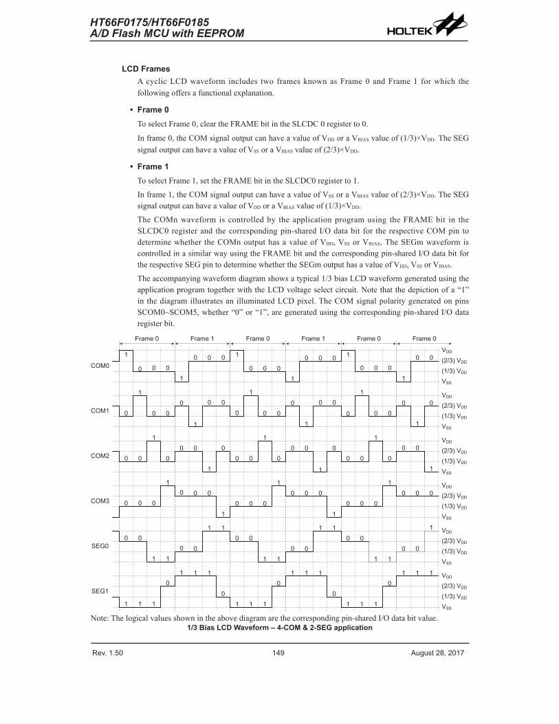
Rev. 1.50 14� ����st ��� �01� Rev. 1.50 149 ����st ��� �01�
HT66F0175/HT66F0185A/D Flash MCU with EEPROM
HT66F0175/HT66F0185A/D Flash MCU with EEPROM
LCD FramesAcyclicLCDwaveform includes two framesknownasFrame0andFrame1 forwhich thefollowingoffersafunctionalexplanation.
• Frame 0ToselectFrame0,cleartheFRAMEbitintheSLCDC0registerto0.
Inframe0,theCOMsignaloutputcanhaveavalueofVDDoraVBIASvalueof(1/3)×VDD.TheSEGsignaloutputcanhaveavalueofVSSoraVBIASvalueof(2/3)×VDD.
• Frame 1ToselectFrame1,settheFRAMEbitintheSLCDC0registerto1.
Inframe1,theCOMsignaloutputcanhaveavalueofVSSoraVBIASvalueof(2/3)×VDD.TheSEGsignaloutputcanhaveavalueofVDDoraVBIASvalueof(1/3)×VDD.
TheCOMnwaveform is controlledby theapplicationprogramusing theFRAMEbit in theSLCDC0registerand thecorrespondingpin-sharedI/Odatabit for therespectiveCOMpin todeterminewhether theCOMnoutputhasavalueofVDD,VSSorVBIAS.TheSEGmwaveformiscontrolledinasimilarwayusingtheFRAMEbitandthecorrespondingpin-sharedI/OdatabitfortherespectiveSEGpintodeterminewhethertheSEGmoutputhasavalueofVDD,VSSorVBIAS.
Theaccompanyingwaveformdiagramshowsatypical1/3biasLCDwaveformgeneratedusingtheapplicationprogramtogetherwiththeLCDvoltageselectcircuit.Notethatthedepictionofa“1”in thediagramillustratesanilluminatedLCDpixel.TheCOMsignalpolaritygeneratedonpinsSCOM0~SCOM5,whether“0”or“1”,aregeneratedusingthecorrespondingpin-sharedI/Odataregisterbit.
COM0
VDD
(2/3) VDD
(1/3) VDD
VSS
VDD
(2/3) VDD
(1/3) VDD
VSS
COM1
COM2
VDD
(2/3) VDD
(1/3) VDD
VSS
VDD
(2/3) VDD
(1/3) VDD
VSS
COM3
VDD
(2/3) VDD
(1/3) VDD
VSS
SEG0
VDD
(2/3) VDD
(1/3) VDD
VSS
SEG1
Frame 0 Frame 1 Frame 0 Frame 1 Frame 0 Frame 0
1
0 0 01
0 0 0 1
0 0 01
0 0 0 1
0 0 01
0 0
0
1
0 00 0 0
1
0
1
0 00 0 0
10
1
0 00 0
1
0 0
1
00 0 0
10 0
1
00 0 0
1
0 0
1
00 0
1
0 0 0
10 0 0
10 0 0
10 0 0
10 0 0
10 0 0
0 0
1 10 0
1 10 0
1 10 0
1 10 0
1 10 0
1
1 1 1
01 1 1
01 1 1
01 1 1
01 1 1
01 1 1
Note:Thelogicalvaluesshownintheabovediagramarethecorrespondingpin-sharedI/Odatabitvalue.1/3 Bias LCD Waveform – 4-COM & 2-SEG application
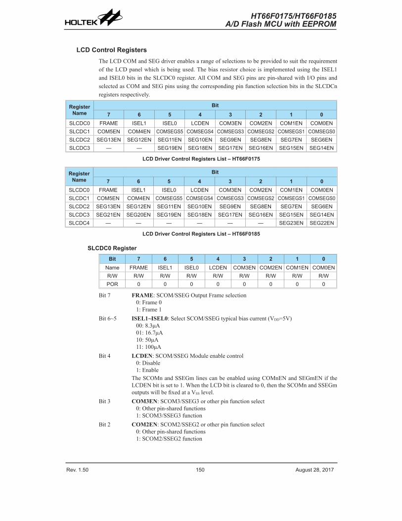
Rev. 1.50 150 ����st ��� �01� Rev. 1.50 151 ����st ��� �01�
HT66F0175/HT66F0185A/D Flash MCU with EEPROM
HT66F0175/HT66F0185A/D Flash MCU with EEPROM
LCD Control RegistersTheLCDCOMandSEGdriverenablesarangeofselectionstobeprovidedtosuittherequirementof theLCDpanelwhichisbeingused.Thebiasresistorchoiceis implementedusingtheISEL1andISEL0bitsintheSLCDC0register.AllCOMandSEGpinsarepin-sharedwithI/OpinsandselectedasCOMandSEGpinsusingthecorrespondingpinfunctionselectionbitsintheSLCDCnregistersrespectively.
Register Name
Bit
7 6 5 4 3 2 1 0SLCDC0 FR�ME ISEL1 ISEL0 LCDEN COM3EN COM�EN COM1EN COM0ENSLCDC1 COM5EN COM4EN COMSEGS5 COMSEGS4 COMSEGS3 COMSEGS� COMSEGS1 COMSEGS0SLCDC� SEG13EN SEG1�EN SEG11EN SEG10EN SEG9EN SEG�EN SEG�EN SEG6ENSLCDC3 — — SEG19EN SEG1�EN SEG1�EN SEG16EN SEG15EN SEG14EN
LCD Driver Control Registers List – HT66F0175
Register Name
Bit
7 6 5 4 3 2 1 0SLCDC0 FR�ME ISEL1 ISEL0 LCDEN COM3EN COM�EN COM1EN COM0ENSLCDC1 COM5EN COM4EN COMSEGS5 COMSEGS4 COMSEGS3 COMSEGS� COMSEGS1 COMSEGS0SLCDC� SEG13EN SEG1�EN SEG11EN SEG10EN SEG9EN SEG�EN SEG�EN SEG6ENSLCDC3 SEG�1EN SEG�0EN SEG19EN SEG1�EN SEG1�EN SEG16EN SEG15EN SEG14ENSLCDC4 — — — — — — SEG�3EN SEG��EN
LCD Driver Control Registers List – HT66F0185
SLCDC0 Register
Bit 7 6 5 4 3 2 1 0Name FR�ME ISEL1 ISEL0 LCDEN COM3EN COM�EN COM1EN COM0ENR/W R/W R/W R/W R/W R/W R/W R/W R/WPOR 0 0 0 0 0 0 0 0
Bit7 FRAME:SCOM/SSEGOutputFrameselection0:Frame01:Frame1
Bit6~5 ISEL1~ISEL0:SelectSCOM/SSEGtypicalbiascurrent(VDD=5V)00:8.3μA01:16.7μA10:50μA11:100μA
Bit4 LCDEN:SCOM/SSEGModuleenablecontrol0:Disable1:Enable
TheSCOMnandSSEGmlinescanbeenabledusingCOMnENandSEGmENiftheLCDENbitissetto1.WhentheLCDbitisclearedto0,thentheSCOMnandSSEGmoutputswillbefixedataVSSlevel.
Bit3 COM3EN:SCOM3/SSEG3orotherpinfunctionselect0:Otherpin-sharedfunctions1:SCOM3/SSEG3function
Bit2 COM2EN:SCOM2/SSEG2orotherpinfunctionselect0:Otherpin-sharedfunctions1:SCOM2/SSEG2function

Rev. 1.50 150 ����st ��� �01� Rev. 1.50 151 ����st ��� �01�
HT66F0175/HT66F0185A/D Flash MCU with EEPROM
HT66F0175/HT66F0185A/D Flash MCU with EEPROM
Bit1 COM1EN:SCOM1/SSEG1orotherpinfunctionselect0:Otherpin-sharedfunctions1:SCOM1/SSEG1function
Bit0 COM0EN:SCOM0/SSEG0orotherpinfunctionselect0:Otherpin-sharedfunctions1:SCOM0/SSEG0function
SLCDC1 Register
Bit 7 6 5 4 3 2 1 0Name COM5EN COM4EN COMSEGS5 COMSEGS4 COMSEGS3 COMSEGS� COMSEGS1 COMSEGS0R/W R/W R/W R/W R/W R/W R/W R/W R/WPOR 0 0 0 0 0 0 0 0
Bit7 COM5EN:SCOM5/SSEG5orotherpinfunctionselect0:Otherpin-sharedfunctions1:SCOM5/SSEG5function
Bit6 COM4EN:SCOM4/SSEG4orotherpinfunctionselect0:Otherpin-sharedfunctions1:SCOM4/SSEG4function
Bit5 COMSEGS5:SCOM5orSSEG5pinfunctionselect0:SCOM51:SSEG5
Bit4 COMSEGS4:SCOM4orSSEG4pinfunctionselect0:SCOM41:SSEG4
Bit3 COMSEGS3:SCOM3orSSEG3pinfunctionselect0:SCOM31:SSEG3
Bit2 COMSEGS2:SCOM2orSSEG2pinfunctionselect0:SCOM21:SSEG2
Bit1 COMSEGS1:SCOM1orSSEG1pinfunctionselect0:SCOM11:SSEG1
Bit0 COMSEGS0:SCOM0orSSEG0pinfunctionselect0:SCOM01:SSEG0
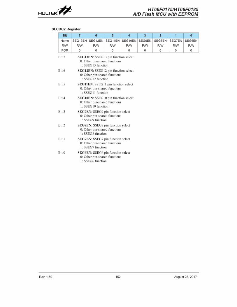
Rev. 1.50 15� ����st ��� �01� Rev. 1.50 153 ����st ��� �01�
HT66F0175/HT66F0185A/D Flash MCU with EEPROM
HT66F0175/HT66F0185A/D Flash MCU with EEPROM
SLCDC2 Register
Bit 7 6 5 4 3 2 1 0Name SEG13EN SEG1�EN SEG11EN SEG10EN SEG9EN SEG�EN SEG�EN SEG6ENR/W R/W R/W R/W R/W R/W R/W R/W R/WPOR 0 0 0 0 0 0 0 0
Bit7 SEG13EN:SSEG13pinfunctionselect0:Otherpin-sharedfunctions1:SSEG13function
Bit6 SEG12EN:SSEG12pinfunctionselect0:Otherpin-sharedfunctions1:SSEG12function
Bit5 SEG11EN:SSEG11pinfunctionselect0:Otherpin-sharedfunctions1:SSEG11function
Bit4 SEG10EN:SSEG10pinfunctionselect0:Otherpin-sharedfunctions1:SSEG10function
Bit3 SEG9EN:SSEG9pinfunctionselect0:Otherpin-sharedfunctions1:SSEG9function
Bit2 SEG8EN:SSEG8pinfunctionselect0:Otherpin-sharedfunctions1:SSEG8function
Bit1 SEG7EN:SSEG7pinfunctionselect0:Otherpin-sharedfunctions1:SSEG7function
Bit0 SEG6EN:SSEG6pinfunctionselect0:Otherpin-sharedfunctions1:SSEG6function

Rev. 1.50 15� ����st ��� �01� Rev. 1.50 153 ����st ��� �01�
HT66F0175/HT66F0185A/D Flash MCU with EEPROM
HT66F0175/HT66F0185A/D Flash MCU with EEPROM
SLCDC3 Register – HT66F0175
Bit 7 6 5 4 3 2 1 0Name — — SEG19EN SEG1�EN SEG1�EN SEG16EN SEG15EN SEG14ENR/W — — R/W R/W R/W R/W R/W R/WPOR — — 0 0 0 0 0 0
Bit7~6 Unimplemented,readas“0”Bit5 SEG19EN:SSEG19pinfunctionselect
0:Otherpin-sharedfunctions1:SSEG19function
Bit4 SEG18EN:SSEG18pinfunctionselect0:Otherpin-sharedfunctions1:SSEG18function
Bit3 SEG17EN:SSEG17pinfunctionselect0:Otherpin-sharedfunctions1:SSEG17function
Bit2 SEG16EN:SSEG16pinfunctionselect0:Otherpin-sharedfunctions1:SSEG16function
Bit1 SEG15EN:SSEG15pinfunctionselect0:Otherpin-sharedfunctions1:SSEG15function
Bit0 SEG14EN:SSEG14pinfunctionselect0:Otherpin-sharedfunctions1:SSEG14function

Rev. 1.50 154 ����st ��� �01� Rev. 1.50 155 ����st ��� �01�
HT66F0175/HT66F0185A/D Flash MCU with EEPROM
HT66F0175/HT66F0185A/D Flash MCU with EEPROM
SLCDC3 Register – HT66F0185
Bit 7 6 5 4 3 2 1 0Name SEG�1EN SEG�0EN SEG19EN SEG1�EN SEG1�EN SEG16EN SEG15EN SEG14ENR/W R/W R/W R/W R/W R/W R/W R/W R/WPOR 0 0 0 0 0 0 0 0
Bit7 SEG21EN:SSEG21pinfunctionselect0:Otherpin-sharedfunctions1:SSEG21function
Bit6 SEG20EN:SSEG20pinfunctionselect0:Otherpin-sharedfunctions1:SSEG20function
Bit5 SEG19EN:SSEG19pinfunctionselect0:Otherpin-sharedfunctions1:SSEG19function
Bit4 SEG18EN:SSEG18pinfunctionselect0:Otherpin-sharedfunctions1:SSEG18function
Bit3 SEG17EN:SSEG17pinfunctionselect0:Otherpin-sharedfunctions1:SSEG17function
Bit2 SEG16EN:SSEG16pinfunctionselect0:Otherpin-sharedfunctions1:SSEG16function
Bit1 SEG15EN:SSEG15pinfunctionselect0:Otherpin-sharedfunctions1:SSEG15function
Bit0 SEG14EN:SSEG14pinfunctionselect0:Otherpin-sharedfunctions1:SSEG14function
SLCDC4 Register – HT66F0185
Bit 7 6 5 4 3 2 1 0Name — — — — — — SEG�3EN SEG��ENR/W — — — — — — R/W R/WPOR — — — — — — 0 0
Bit7~2 Unimplemented,readas“0”Bit1 SEG23EN:SSEG23pinfunctionselect
0:Otherpin-sharedfunctions1:SSEG23function
Bit0 SEG22EN:SSEG22pinfunctionselect0:Otherpin-sharedfunctions1:SSEG22function
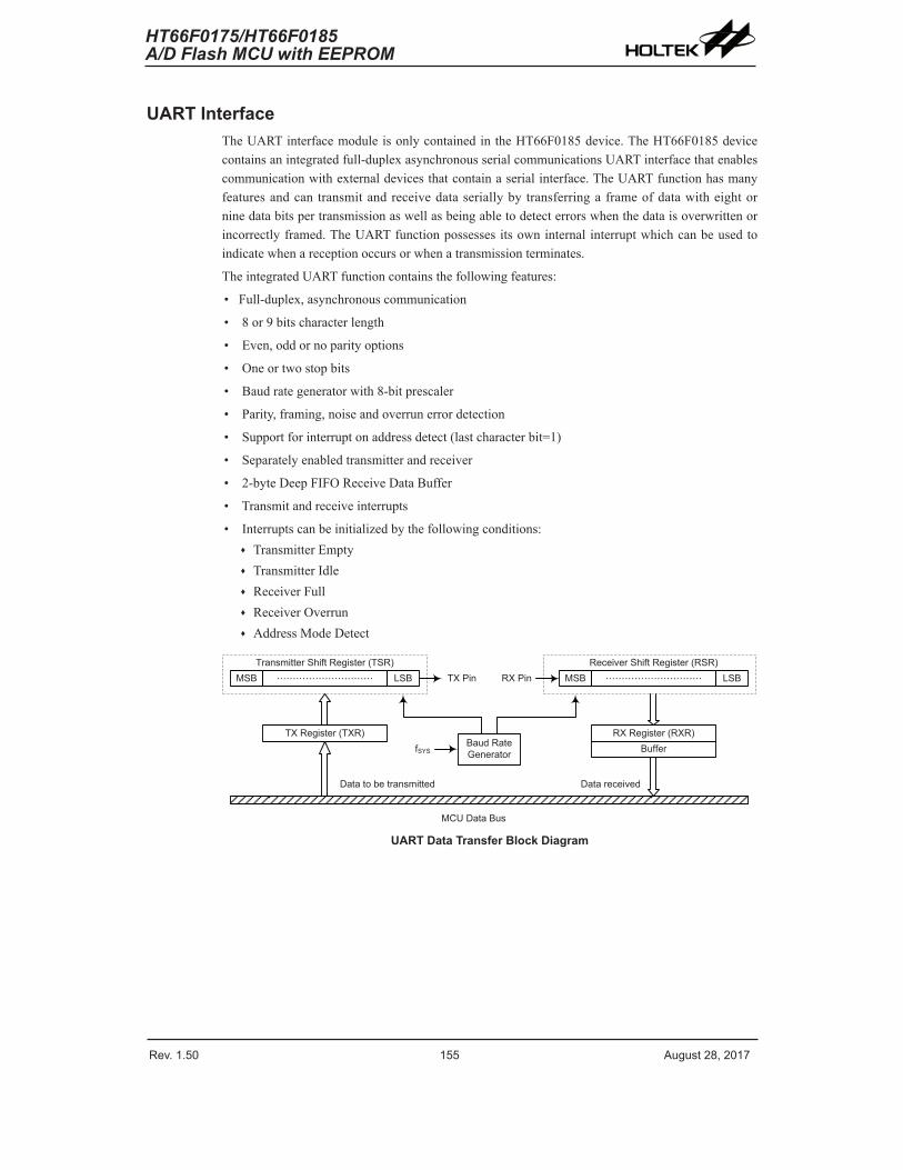
Rev. 1.50 154 ����st ��� �01� Rev. 1.50 155 ����st ��� �01�
HT66F0175/HT66F0185A/D Flash MCU with EEPROM
HT66F0175/HT66F0185A/D Flash MCU with EEPROM
UART InterfaceTheUARTinterfacemoduleisonlycontainedintheHT66F0185device.TheHT66F0185devicecontainsanintegratedfull-duplexasynchronousserialcommunicationsUARTinterfacethatenablescommunicationwithexternaldevicesthatcontainaserialinterface.TheUARTfunctionhasmanyfeaturesandcantransmitandreceivedataseriallyby transferringaframeofdatawitheightorninedatabitspertransmissionaswellasbeingabletodetecterrorswhenthedataisoverwrittenorincorrectlyframed.TheUARTfunctionpossessesitsowninternal interruptwhichcanbeusedtoindicatewhenareceptionoccursorwhenatransmissionterminates.
TheintegratedUARTfunctioncontainsthefollowingfeatures:
• Full-duplex,asynchronouscommunication
• 8or9bitscharacterlength
• Even,oddornoparityoptions
• Oneortwostopbits
• Baudrategeneratorwith8-bitprescaler
• Parity,framing,noiseandoverrunerrordetection
• Supportforinterruptonaddressdetect(lastcharacterbit=1)
• Separatelyenabledtransmitterandreceiver
• 2-byteDeepFIFOReceiveDataBuffer
• Transmitandreceiveinterrupts
• Interruptscanbeinitializedbythefollowingconditions:♦ TransmitterEmpty♦ TransmitterIdle♦ ReceiverFull♦ ReceiverOverrun♦ AddressModeDetect
MSB LSB…………………………
Transmitter Shift Re�ister (TSR)MSB LSB…………………………
Receiver Shift Re�ister (RSR)TX Pin RX Pin
Ba�d Rate Generator
TX Re�ister (TXR) RX Re�ister (RXR)
Data to be transmitted Data received
B�fferfSYS
MCU Data B�s
UART Data Transfer Block Diagram

Rev. 1.50 156 ����st ��� �01� Rev. 1.50 15� ����st ��� �01�
HT66F0175/HT66F0185A/D Flash MCU with EEPROM
HT66F0175/HT66F0185A/D Flash MCU with EEPROM
UART External PinTocommunicatewithanexternalserialinterface,theinternalUARThastwoexternalpinsknownasTXandRX.TheTXandRXpinsarerespectivelytheUARTtransmitterandreceiverpinswhicharepin-sharedwithI/Oorotherpin-sharedfunctions.AlongwiththeUARTENbit,theTXENandRXENbits,ifset,willautomaticallysetuptheseI/OpinstotheirrespectiveTXoutputandRXinputconditionsanddisableanypull-highresistoroptionwhichmayexistontheTXandRXpins.WhentheTXorRXpinfunctionisdisabledbyclearingtheUARTEN,TXENorRXENbit,theTXorRXpinwillbeusedasI/Oorotherpin-sharedfunctionalpindependinguponthepin-sharedfunctionpriority.
UART Data Transfer SchemeTheabovediagramshowstheoveralldatatransferstructurearrangementfortheUARTinterface.Theactualdata tobe transmittedfromtheMCUis first transferred to theTXRregisterby theapplicationprogram.ThedatawillthenbetransferredtotheTransmitShiftRegisterfromwhereitwillbeshiftedout,LSBfirst,ontotheTXpinataratecontrolledbytheBaudRateGenerator.OnlytheTXRregisterismappedontotheMCUDataMemory,theTransmitShiftRegisterisnotmappedandisthereforeinaccessibletotheapplicationprogram.
DatatobereceivedbytheUARTisacceptedontheexternalRXpin,fromwhereit isshiftedin,LSBfirst, to theReceiverShiftRegisterataratecontrolledbytheBaudRateGenerator.Whentheshiftregisterisfull,thedatawillthenbetransferredfromtheshiftregistertotheinternalRXRregister,whereit isbufferedandcanbemanipulatedbytheapplicationprogram.OnlytheTXRregisterismappedontotheMCUDataMemory,theReceiverShiftRegisterisnotmappedandisthereforeinaccessibletotheapplicationprogram.
Itshouldbenotedthattheactualregisterfordatatransmissionandreception,althoughreferredtointhetext,andinapplicationprograms,asseparateTXRandRXRregisters,onlyexistsasasinglesharedregisterintheDataMemory.ThissharedregisterknownastheTXR_RXRregisterisusedforbothdatatransmissionanddatareception.
UART Status and Control RegistersTherearefivecontrolregistersassociatedwiththeUARTfunction.TheUSR,UCR1andUCR2registerscontroltheoverallfunctionoftheUART,whiletheBRGregistercontrolstheBaudrate.TheactualdatatobetransmittedandreceivedontheserialinterfaceismanagedthroughtheTXR_RXRdataregisters.
Register Name
Bit
7 6 5 4 3 2 1 0USR PERR NF FERR OERR RIDLE RXIF TIDLE TXIF
UCR1 U�RTEN BNO PREN PRT STOPS TXBRK RX� TX�UCR� TXEN RXEN BRGH �DDEN W�KE RIE TIIE TEIEBRG BRG� BRG6 BRG5 BRG4 BRG3 BRG� BRG1 BRG0
TXR_RXR TXRX� TXRX6 TXRX5 TXRX4 TXRX3 TXRX� TXRX1 TXRX0
UART Status and Control Registers List – HT66F0185 only

Rev. 1.50 156 ����st ��� �01� Rev. 1.50 15� ����st ��� �01�
HT66F0175/HT66F0185A/D Flash MCU with EEPROM
HT66F0175/HT66F0185A/D Flash MCU with EEPROM
TXR_RXR RegisterTheTXR_RXRregisteristhedataregisterwhichisusedtostorethedatatobetransmittedontheTXpinorbeingreceivedfromtheRXpin.
Bit 7 6 5 4 3 2 1 0Name TXRX� TXRX6 TXRX5 TXRX4 TXRX3 TXRX� TXRX1 TXRX0R/W R/W R/W R/W R/W R/W R/W R/W R/WPOR x x x x x x x x
“x”: �nknown
Bit7~0 TXRX7~TXRX0:UARTTransmit/ReceiveDatabits
USR RegisterTheUSR register is the status register for theUART,whichcanbe readby theprogram todeterminethepresentstatusoftheUART.AllflagswithintheUSRregisterarereadonlyandfurtherexplanationsaregivenbelow.
Bit 7 6 5 4 3 2 1 0Name PERR NF FERR OERR RIDLE RXIF TIDLE TXIFR/W R R R R R R R RPOR 0 0 0 0 1 0 1 1
Bit7 PERR:Parityerrorflag0:Noparityerrorisdetected1:Parityerrorisdetected
ThePERRflagistheparityerrorflag.Whenthisreadonlyflagis“0”,itindicatesaparityerrorhasnotbeendetected.Whentheflagis“1”,itindicatesthattheparityofthereceivedwordisincorrect.ThiserrorflagisapplicableonlyifParitymode(oddoreven)isselected.TheflagcanalsobeclearedbyasoftwaresequencewhichinvolvesareadtothestatusregisterUSRfollowedbyanaccesstotheRXRdataregister.
Bit6 NF:Noiseflag0:Nonoiseisdetected1:Noiseisdetected
TheNFflagis thenoiseflag.Whenthisreadonlyflagis“0”, it indicatesnonoisecondition.Whentheflagis“1”,itindicatesthattheUARThasdetectednoiseonthereceiverinput.TheNFflagissetduringthesamecycleastheRXIFflagbutwillnotbesetinthecaseofasoverrun.TheNFflagcanbeclearedbyasoftwaresequencewhichwillinvolveareadtothestatusregisterUSRfollowedbyanaccesstotheRXRdataregister.
Bit5 FERR:Framingerrorflag0:Noframingerrorisdetected1:Framingerrorisdetected
TheFERRflagistheframingerrorflag.Whenthisreadonlyflagis“0”,itindicatesthat thereisnoframingerror.Whentheflagis“1”, it indicates thataframingerrorhasbeendetectedforthecurrentcharacter.TheflagcanalsobeclearedbyasoftwaresequencewhichwillinvolveareadtothestatusregisterUSRfollowedbyanaccesstotheRXRdataregister.

Rev. 1.50 15� ����st ��� �01� Rev. 1.50 159 ����st ��� �01�
HT66F0175/HT66F0185A/D Flash MCU with EEPROM
HT66F0175/HT66F0185A/D Flash MCU with EEPROM
Bit4 OERR:Overrunerrorflag0:Nooverrunerrorisdetected1:Overrunerrorisdetected
TheOERRflagistheoverrunerrorflagwhichindicateswhenthereceiverbufferhasoverflowed.Whenthisreadonlyflagis“0”,itindicatesthatthereisnooverrunerror.Whentheflagis“1”,itindicatesthatanoverrunerroroccurswhichwillinhibitfurthertransferstotheRXRreceivedataregister.Theflagisclearedbyasoftwaresequence,which isa read to thestatusregisterUSRfollowedbyanaccess to theRXRdataregister.
Bit3 RIDLE:Receiverstatus0:Datareceptionisinprogress(databeingreceived)1:Nodatareceptionisinprogress(receiverisidle)
TheRIDLEflagisthereceiverstatusflag.Whenthisreadonlyflagis“0”,itindicatesthatthereceiverisbetweentheinitialdetectionofthestartbitandthecompletionofthestopbit.Whentheflagis“1”, it indicates that thereceiver is idle.Betweenthecompletionofthestopbitandthedetectionofthenextstartbit,theRIDLEbitis“1”indicatingthattheUARTreceiverisidleandtheRXpinstaysinlogichighcondition.
Bit2 RXIF:ReceiveRXRdataregisterstatus0:RXRdataregisterisempty1:RXRdataregisterhasavailabledata
TheRXIFflagisthereceivedataregisterstatusflag.Whenthisreadonlyflagis“0”,itindicatesthattheRXRreaddataregisterisempty.Whentheflagis“1”,itindicatesthat theRXRreaddataregistercontainsnewdata.When thecontentsof theshiftregisteraretransferredtotheRXRregister,aninterruptisgeneratedifRIE=1intheUCR2register.Ifoneormoreerrorsaredetectedinthereceivedword,theappropriatereceive-relatedflagsNF,FERR,and/orPERRaresetwithinthesameclockcycle.TheRXIFflagisclearedwhentheUSRregisterisreadwithRXIFset,followedbyareadfromtheRXRregister,andiftheRXRregisterhasnodataavailable.
Bit1 TIDLE:Transmissionstatus0:Datatransmissionisinprogress(databeingtransmitted)1:Nodatatransmissionisinprogress(transmitterisidle)
TheTIDLEflag isknownas the transmissioncompleteflag.Whenthis readonlyflagis“0”,it indicatesthatatransmissionisinprogress.Thisflagwillbesetto“1”whentheTXIFflagis“1”andwhenthereisnotransmitdataorbreakcharacterbeingtransmitted.WhenTIDLEisequalto1, theTXpinbecomesidlewiththepinstateinlogichighcondition.TheTIDLEflagisclearedbyreadingtheUSRregisterwithTIDLEsetandthenwritingtotheTXRregister.Theflagisnotgeneratedwhenadatacharacterorabreakisqueuedandreadytobesent.
Bit0 TXIF:TransmitTXRdataregisterstatus0:Characterisnottransferredtothetransmitshiftregister1:Characterhastransferredtothetransmitshiftregister(TXRdataregisterisempty)
TheTXIFflagisthetransmitdataregisteremptyflag.Whenthisreadonlyflagis“0”,itindicatesthatthecharacterisnottransferredtothetransmittershiftregister.Whentheflagis“1”,it indicatesthatthetransmittershiftregisterhasreceivedacharacterfromtheTXRdataregister.TheTXIFflag isclearedbyreadingtheUARTstatusregister(USR)withTXIFsetandthenwriting to theTXRdataregister.Note thatwhentheTXENbit isset, theTXIFflagbitwillalsobesetsincethetransmitdataregisterisnotyetfull.
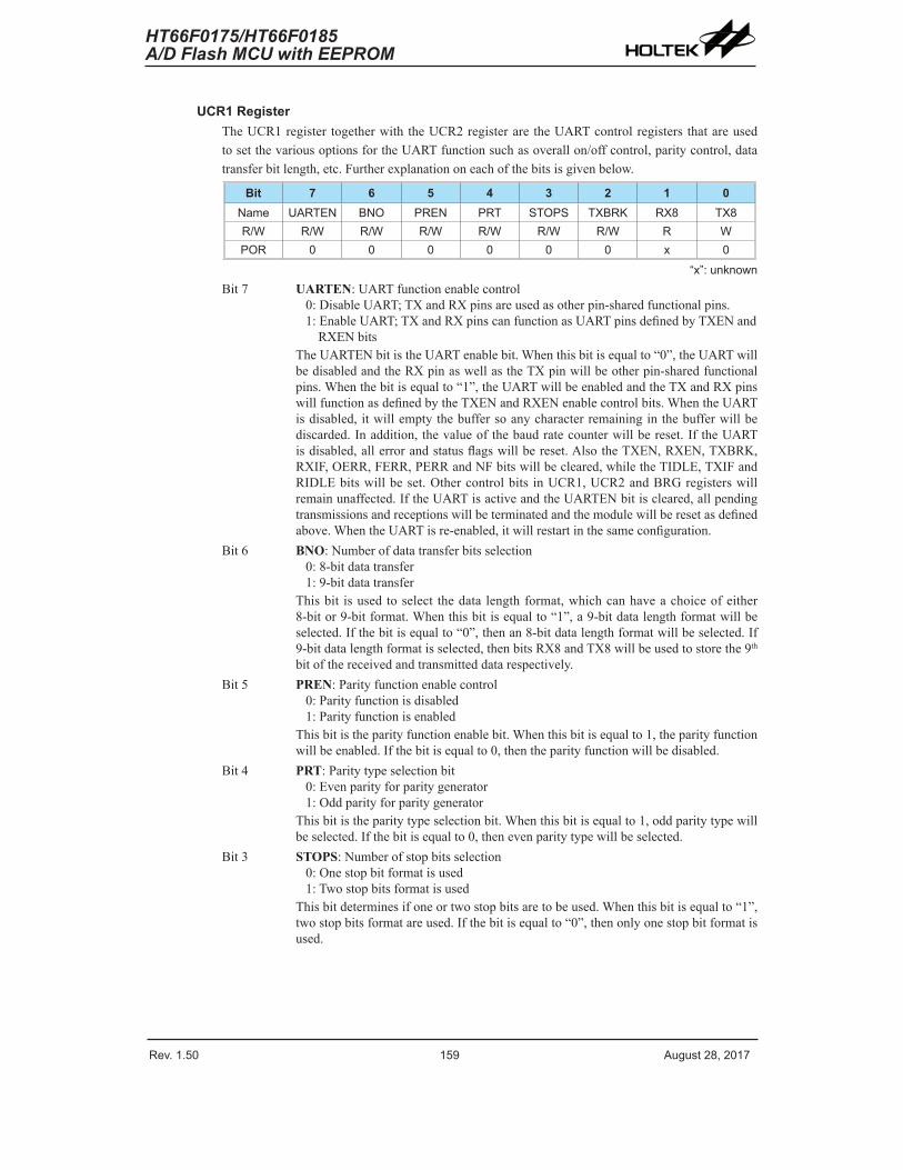
Rev. 1.50 15� ����st ��� �01� Rev. 1.50 159 ����st ��� �01�
HT66F0175/HT66F0185A/D Flash MCU with EEPROM
HT66F0175/HT66F0185A/D Flash MCU with EEPROM
UCR1 RegisterTheUCR1register togetherwiththeUCR2registeraretheUARTcontrolregisters thatareusedtosetthevariousoptionsfortheUARTfunctionsuchasoverallon/offcontrol,paritycontrol,datatransferbitlength,etc.Furtherexplanationoneachofthebitsisgivenbelow.
Bit 7 6 5 4 3 2 1 0Name U�RTEN BNO PREN PRT STOPS TXBRK RX� TX�R/W R/W R/W R/W R/W R/W R/W R WPOR 0 0 0 0 0 0 x 0
“x”: �nknownBit7 UARTEN:UARTfunctionenablecontrol
0:DisableUART;TXandRXpinsareusedasotherpin-sharedfunctionalpins.1:EnableUART;TXandRXpinscanfunctionasUARTpinsdefinedbyTXENandRXENbits
TheUARTENbitistheUARTenablebit.Whenthisbitisequalto“0”,theUARTwillbedisabledandtheRXpinaswellastheTXpinwillbeotherpin-sharedfunctionalpins.Whenthebitisequalto“1”,theUARTwillbeenabledandtheTXandRXpinswillfunctionasdefinedbytheTXENandRXENenablecontrolbits.WhentheUARTisdisabled,itwillemptythebuffersoanycharacterremaininginthebufferwillbediscarded.Inaddition,thevalueofthebaudratecounterwillbereset.If theUARTisdisabled,allerrorandstatusflagswillbereset.AlsotheTXEN,RXEN,TXBRK,RXIF,OERR,FERR,PERRandNFbitswillbecleared,whiletheTIDLE,TXIFandRIDLEbitswillbeset.Othercontrolbits inUCR1,UCR2andBRGregisterswillremainunaffected.IftheUARTisactiveandtheUARTENbitiscleared,allpendingtransmissionsandreceptionswillbeterminatedandthemodulewillberesetasdefinedabove.WhentheUARTisre-enabled,itwillrestartinthesameconfiguration.
Bit6 BNO:Numberofdatatransferbitsselection0:8-bitdatatransfer1:9-bitdatatransfer
Thisbit isusedtoselect thedata lengthformat,whichcanhaveachoiceofeither8-bitor9-bitformat.Whenthisbitisequalto“1”,a9-bitdatalengthformatwillbeselected.Ifthebitisequalto“0”,thenan8-bitdatalengthformatwillbeselected.If9-bitdatalengthformatisselected,thenbitsRX8andTX8willbeusedtostorethe9thbitofthereceivedandtransmitteddatarespectively.
Bit5 PREN:Parityfunctionenablecontrol0:Parityfunctionisdisabled1:Parityfunctionisenabled
Thisbitistheparityfunctionenablebit.Whenthisbitisequalto1,theparityfunctionwillbeenabled.Ifthebitisequalto0,thentheparityfunctionwillbedisabled.
Bit4 PRT:Paritytypeselectionbit0:Evenparityforparitygenerator1:Oddparityforparitygenerator
Thisbitistheparitytypeselectionbit.Whenthisbitisequalto1,oddparitytypewillbeselected.Ifthebitisequalto0,thenevenparitytypewillbeselected.
Bit3 STOPS:Numberofstopbitsselection0:Onestopbitformatisused1:Twostopbitsformatisused
Thisbitdeterminesifoneortwostopbitsaretobeused.Whenthisbitisequalto“1”,twostopbitsformatareused.Ifthebitisequalto“0”,thenonlyonestopbitformatisused.

Rev. 1.50 160 ����st ��� �01� Rev. 1.50 161 ����st ��� �01�
HT66F0175/HT66F0185A/D Flash MCU with EEPROM
HT66F0175/HT66F0185A/D Flash MCU with EEPROM
Bit2 TXBRK:Transmitbreakcharacter0:Nobreakcharacteristransmitted1:Breakcharacterstransmit
TheTXBRKbit is theTransmitBreakCharacterbit.Whenthisbit isequal to“0”,therearenobreakcharactersandtheTXpinoperatsnormally.Whenthebitisequalto“1”,therearetransmitbreakcharactersandthetransmitterwillsendlogiczeros.Whenthisbit isequal to“1”,after thebuffereddatahasbeentransmitted, thetransmitteroutputisheldlowforaminimumofa13-bitlengthanduntiltheTXBRKbitisreset.
Bit1 RX8:Receivedatabit8for9-bitdatatransferformat(readonly)Thisbitisonlyusedif9-bitdatatransfersareused,inwhichcasethisbitlocationwillstorethe9thbitofthereceiveddataknownasRX8.TheBNObitisusedtodeterminewhetherdatatransfesarein8-bitor9-bitformat.
Bit0 TX8:Transmitdatabit8for9-bitdatatransferformat(writeonly)Thisbit isonlyusedif9-bitdata transfersareused, inwhichcasethisbit locationwillstorethe9thbitof thetransmitteddataknownasTX8.TheBNObit isusedtodeterminewhetherdatatransfesarein8-bitor9-bitformat.
UCR2 RegisterTheUCR2registeris thesecondoftheUARTcontrolregistersandservesseveralpurposes.Oneofitsmainfunctionsistocontrolthebasicenable/disableoperationif theUARTTransmitterandReceiveraswellasenablingthevariousUARTinterruptsources.Theregisteralsoservestocontrolthebaudratespeed, receiverwake-upfunctionenableand theaddressdetect functionenable.Furtherexplanationoneachofthebitsisgivenbelow.
Bit 7 6 5 4 3 2 1 0Name TXEN RXEN BRGH �DDEN W�KE RIE TIIE TEIER/W R/W R/W R/W R/W R/W R/W R/W R/WPOR 0 0 0 0 0 0 0 0
Bit7 TXEN:UARTTransmitterenablecontrol0:UARTTransmitterisdisabled1:UARTTransmitterisenabled
TheTXENbit is theTransmitterEnableBit.When thisbit is equal to“0”, thetransmitterwillbedisabledwithanypendingdata transmissionsbeingaborted. Inadditionthebufferswillbereset.InthissituationtheTXpinwillbeotherpin-sharedfunctionalpin.IftheTXENbitisequalto“1”andtheUARTENbitisalsoequalto1, the transmitterwillbeenabledandtheTXpinwillbecontrolledbytheUART.ClearingtheTXENbitduringatransmissionwillcausethedatatransmissiontobeabortedandwillresetthetransmitter.Ifthissituationoccurs,theTXpinwillbeotherpin-sharedfunctionalpin.
Bit6 RXEN:UARTReceiverenablecontrol0:UARTReceiverisdisabled1:UARTReceiverisenabled
TheRXENbitistheReceiverEnableBit.Whenthisbitisequalto“0”,thereceiverwillbedisabledwithanypendingdata receptionsbeingaborted. Inaddition thereceiverbufferswillbereset. In thissituation theRXpinwillbeotherpin-sharedfunctionalpin. If theRXENbit isequal to“1”andtheUARTENbit isalsoequalto1, thereceiverwillbeenabledandtheRXpinwillbecontrolledbytheUART.ClearingtheRXENbitduringareceptionwillcausethedatareceptiontobeabortedandwillresetthereceiver.Ifthissituationoccurs,theRXpinwillbeotherpin-sharedfunctionalpin.

Rev. 1.50 160 ����st ��� �01� Rev. 1.50 161 ����st ��� �01�
HT66F0175/HT66F0185A/D Flash MCU with EEPROM
HT66F0175/HT66F0185A/D Flash MCU with EEPROM
Bit5 BRGH:BaudRatespeedselection0:Lowspeedbaudrate1:Highspeedbaudrate
ThebitnamedBRGHselectsthehighorlowspeedmodeoftheBaudRateGenerator.Thisbit, togetherwiththevalueplacedinthebaudrateregister,BRG,controls thebaudrateoftheUART.Ifthebitisequalto0,thelowspeedmodeisselected.
Bit4 ADDEN:Addressdetectfunctionenablecontrol0:Addressdetectionfunctionisdisabled1:Addressdetectionfunctionisenabled
ThebitnamedADDENistheaddressdetectionfunctionenablecontrolbit.Whenthisbit isequalto1,theaddressdetectionfunctionisenabled.Whenitoccurs,if the8thbit,whichcorrespondstoRX7ifBNO=0,orthe9thbit,whichcorrespondstoRX8ifBNO=1,hasavalueof“1”,thenthereceivedwordwillbeidentifiedasanaddress,ratherthandata.Ifthecorrespondinginterruptisenabled,aninterruptrequestwillbegeneratedeachtimethereceivedwordhastheaddressbitset,whichisthe8thor9thbitdependingonthevalueoftheBNObit.If theaddressbitknownasthe8thor9thbitofthereceivedwordis“0”withtheaddressdetectionfunctionbeingenabled,aninterruptwillnotbegeneratedandthereceiveddatawillbediscarded.
Bit3 WAKE:RXpinfallingedgewake-upfunctionenablecontrol0:RXpinwake-upfunctionisdisabled1:RXpinwake-upfunctionisenabled
Thebitenablesordisablesthereceiverwake-upfunction.Ifthisbitisequalto1andthedeviceisinIDLE0orSLEEPmode,afallingedgeontheRXpinwillwakeupthedevice.Ifthisbit isequalto0andthedeviceisinthepowerdownmode,anyedgetransitionsontheRXpinwillnotwakeupthedevice.
Bit2 RIE:Receiverinterruptenablecontrol0:Receiverrelatedinterruptisdisabled1:Receiverrelatedinterruptisenabled
Thebitenablesordisablesthereceiverinterrupt.Ifthisbitisequalto1andwhenthereceiveroverrunflagOERRorreceiveddataavailableflagRXIFisset, theUARTinterruptrequestflagwillbeset.Ifthisbitisequalto0,theUARTinterruptrequestflagwillnotbeinfluencedbytheconditionoftheOERRorRXIFflags.
Bit1 TIIE:TransmitterIdleinterruptenablecontrol0:Transmitteridleinterruptisdisabled1:Transmitteridleinterruptisenabled
Thebitenablesordisablesthetransmitteridleinterrupt.If thisbit isequalto1andwhenthetransmitter idleflagTIDLEisset,duetoa transmitter idlecondition, theUARTinterruptrequestflagwillbeset.If thisbit isequalto0,theUARTinterruptrequestflagwillnotbeinfluencedbytheconditionoftheTIDLEflag.
Bit0 TEIE:TransmitterEmptyinterruptenablecontrol0:Transmitteremptyinterruptisdisabled1:Transmitteremptyinterruptisenabled
Thebitenablesordisablesthetransmitteremptyinterrupt.Ifthisbitisequalto1andwhenthetransmitteremptyflagTXIFisset,duetoatransmitteremptycondition,theUARTinterruptrequestflagwillbeset.If thisbit isequalto0,theUARTinterruptrequestflagwillnotbeinfluencedbytheconditionoftheTXIFflag.
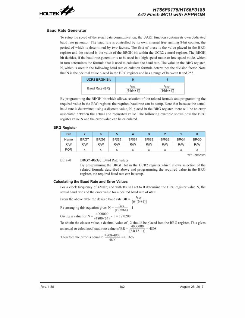
Rev. 1.50 16� ����st ��� �01� Rev. 1.50 163 ����st ��� �01�
HT66F0175/HT66F0185A/D Flash MCU with EEPROM
HT66F0175/HT66F0185A/D Flash MCU with EEPROM
Baud Rate GeneratorTosetupthespeedoftheserialdatacommunication,theUARTfunctioncontainsitsowndedicatedbaudrategenerator.Thebaudrateiscontrolledbyitsowninternalfreerunning8-bitcounter, theperiodofwhichisdeterminedbytwofactors.Thefirstof these is thevalueplacedin theBRGregisterandthesecondisthevalueoftheBRGHbitwithintheUCR2controlregister.TheBRGHbitdecides,ifthebaudrategeneratoristobeusedinahighspeedmodeorlowspeedmode,whichinturndeterminestheformulathatisusedtocalculatethebaudrate.ThevalueintheBRGregister,N,whichisusedinthefollowingbaudratecalculationformuladeterminesthedivisionfactor.NotethatNisthedecimalvalueplacedintheBRGregisterandhasarangeofbetween0and255.
UCR2 BRGH Bit 0 1
Ba�d Rate (BR)fSYS
[64(N+1)]fSYS
[16(N+1)]
ByprogrammingtheBRGHbitwhichallowsselectionoftherelatedformulaandprogrammingtherequiredvalueintheBRGregister,therequiredbaudratecanbesetup.Notethatbecausetheactualbaudrateisdeterminedusingadiscretevalue,N,placedintheBRGregister,therewillbeanerrorassociatedbetweentheactualandrequestedvalue.ThefollowingexampleshowshowtheBRGregistervalueNandtheerrorvaluecanbecalculated.
BRG Register
Bit 7 6 5 4 3 2 1 0Name BRG� BRG6 BRG5 BRG4 BRG3 BRG� BRG1 BRG0R/W R/W R/W R/W R/W R/W R/W R/W R/WPOR x x x x x x x x
“x”: �nknownBit7~0 BRG7~BRG0:BaudRatevalues
ByprogrammingtheBRGHbit intheUCR2registerwhichallowsselectionof therelatedformuladescribedaboveandprogramming therequiredvalue in theBRGregister,therequiredbaudratecanbesetup.
Calculating the Baud Rate and Error ValuesForaclockfrequencyof4MHz,andwithBRGHsetto0determinetheBRGregistervalueN,theactualbaudrateandtheerrorvalueforadesiredbaudrateof4800.
FromtheabovetablethedesiredbaudrateBR= fSYS
[64(N+1)]
Re-arrangingthisequationgivesN= fSYS
(BR×64) -1
GivingavalueforN= 4000000(4800×64) -1=12.0208
Toobtaintheclosestvalue,adecimalvalueof12shouldbeplacedintotheBRGregister.ThisgivesanactualorcalculatedbaudratevalueofBR= 4000000
[64(12+1)]=4808
Thereforetheerrorisequalto 4808-48004800
=0.16%
Rev. 1.50 16� ����st ��� �01� Rev. 1.50 163 ����st ��� �01�
HT66F0175/HT66F0185A/D Flash MCU with EEPROM
HT66F0175/HT66F0185A/D Flash MCU with EEPROM
UART Setup and ControlFordatatransfer,theUARTfunctionutilizesanon-return-to-zero,morecommonlyknownasNRZ,format.Thisiscomposedofonestartbit,eightorninedatabitsandoneor twostopbits.ParityissupportedbytheUARThardwareandcanbesetuptobeeven,oddornoparity.Forthemostcommondataformat,8databitsalongwithnoparityandonestopbit,denotedas8,N,1,isusedasthedefaultsetting,whichisthesettingatpower-on.Thenumberofdatabitsandstopbits,alongwiththeparity,aresetupbyprogrammingthecorrespondingBNO,PRT,PRENandSTOPSbitsintheUCR1register.Thebaudrateusedtotransmitandreceivedataissetupusingtheinternal8-bitbaudrategenerator,whilethedataistransmittedandreceivedLSBfirst.AlthoughthetransmitterandreceiveroftheUARTarefunctionallyindependent,theybothusethesamedataformatandbaudrate.Inallcasesstopbitswillbeusedfordatatransmission.
Enabling/Disabling the UART InterfaceThebasicon/offfunctionoftheinternalUARTfunctioniscontrolledusingtheUARTENbitintheUCR1register.IftheUARTEN,TXENandRXENbitsareset,thenthesetwoUARTpinswillactasnormalTXoutputpinandRXinputpinrespectively.IfnodataisbeingtransmittedontheTXpin,thenitwilldefaulttoalogichighvalue.
ClearingtheUARTENbitwilldisabletheTXandRXpinsandthesetwopinswillbeusedasI/Oorotherpin-sharedfunctionalpins.When theUARTfunction isdisabled, thebufferwillberesettoanemptycondition,atthesametimediscardinganyremainingresidualdata.DisablingtheUARTwillalsoresettheenablecontrol,theerrorandstatusflagswithbitsTXEN,RXEN,TXBRK,RXIF,OERR,FERR,PERRandNFbeingclearedwhilebitsTIDLE,TXIFandRIDLEwillbeset.Theremainingcontrolbits in theUCR1,UCR2andBRGregisterswill remainunaffected.If theUARTENbit in theUCR1register isclearedwhile theUARTisactive, thenallpendingtransmissionsand receptionswillbe immediatelysuspendedand theUARTwillbe reset toaconditionasdefinedabove.IftheUARTisthensubsequentlyre-enabled,itwillrestartagaininthesameconfiguration.
Data, Parity and Stop Bit SelectionTheformatof thedata tobe transferred iscomposedofvariousfactorssuchasdatabit length,parityon/off,paritytype,addressbitsandthenumberofstopbits.ThesefactorsaredeterminedbythesetupofvariousbitswithintheUCR1register.TheBNObitcontrols thenumberofdatabitswhichcanbesettoeither8or9.ThePRTbitcontrolsthechoiceifoddorevenparity.ThePRENbitcontrolstheparityon/offfunction.TheSTOPSbitdecideswhetheroneortwostopbitsaretobeused.Thefollowingtableshowsvariousformatsfordatatransmission.Theaddressdetectmodecontrolbitidentifiestheframeasanaddresscharacter.Thenumberofstopbits,whichcanbeeitheroneortwo,isindependentofthedatalength.
Start Bit Data Bits Address Bits Parity Bit Stop BitExample of 8-bit Data Formats
1 � 0 0 11 � 0 1 11 � 1 0 1
Example of 9-bit Data Formats1 9 0 0 11 � 0 1 11 � 1 0 1
Transmitter Receiver Data Format

Rev. 1.50 164 ����st ��� �01� Rev. 1.50 165 ����st ��� �01�
HT66F0175/HT66F0185A/D Flash MCU with EEPROM
HT66F0175/HT66F0185A/D Flash MCU with EEPROM
Thefollowingdiagramshows the transmitandreceivewaveformsforboth8-bitand9-bitdataformats.
� � � � � � � � � � � � � � � � � � � � � � � � � � � � � � � � � � � � � � � � � � � � � � � � � � � � � � � � �
� � �� � � � �� � �
� � � � � � � � �
� � � � � � � � � � � � � � � � �
� � � � � � � � � � � � � � � � � � � � � � � � � � � � � � � � � � � � � � � � � � � � � � � � � � � � � � � � �
� � �� � � � �� � �
� � � � � � � � �
� � � � � � � � � � � � � � � � �
� � � �
UART TransmitterDatawordlengthsofeither8or9bitscanbeselectedbyprogrammingtheBNObitintheUCR1register.WhenBNObitisset, thewordlengthwillbesetto9bits.Inthiscasethe9thbit,whichistheMSB,needstobestoredintheTX8bitintheUCR1register.AtthetransmittercoreliestheTransmitterShiftRegister,morecommonlyknownas theTSR,whosedata isobtainedfromthetransmitdataregister,whichisknownas theTXRregister.Thedata tobe transmittedis loadedintothisTXRregisterbytheapplicationprogram.TheTSRregisterisnotwrittentowithnewdatauntilthestopbitfromtheprevioustransmissionhasbeensentout.Assoonasthisstopbithasbeentransmitted,theTSRcanthenbeloadedwithnewdatafromtheTXRregister, ifit isavailable.ItshouldbenotedthattheTSRregister,unlikemanyotherregisters, isnotdirectlymappedintotheDataMemoryareaandassuch isnotavailable to theapplicationprogramfordirect read/writeoperations.AnactualtransmissionofdatawillnormallybeenabledwhentheTXENbitisset,butthedatawillnotbetransmitteduntiltheTXRregisterhasbeenloadedwithdataandthebaudrategeneratorhasdefinedashiftclocksource.However,thetransmissioncanalsobeinitiatedbyfirstloadingdataintotheTXRregister,afterwhichtheTXENbitcanbeset.Whenatransmissionofdatabegins,theTSRisnormallyempty,inwhichcaseatransfertotheTXRregisterwillresultinanimmediatetransfertotheTSR.IfduringatransmissiontheTXENbitiscleared,thetransmissionwillimmediatelyceaseandthetransmitterwillbereset.TheTXoutputpinwillthenreturntotheI/Oorotherpin-sharedfunction.
Transmitting DataWhentheUARTistransmittingdata,thedataisshiftedontheTXpinfromtheshiftregister,withtheleastsignificantbitLSBfirst.Inthetransmitmode,theTXRregisterformsabufferbetweentheinternalbusandthetransmittershiftregister.Itshouldbenotedthatif9-bitdataformathasbeenselected,thentheMSBwillbetakenfromtheTX8bitintheUCR1register.Thestepstoinitiateadatatransfercanbesummarizedasfollows:
• MakethecorrectselectionoftheBNO,PRT,PRENandSTOPSbitstodefinetherequiredwordlength,paritytypeandnumberofstopbits.
• SetuptheBRGregistertoselectthedesiredbaudrate.
• Set theTXENbit toensurethat theUARTtransmitterisenabledandtheTXpinisusedasaUARTtransmitterpin.
• AccesstheUSRregisterandwritethedatathatistobetransmittedintotheTXRregister.NotethatthisstepwillcleartheTXIFbit.
Rev. 1.50 164 ����st ��� �01� Rev. 1.50 165 ����st ��� �01�
HT66F0175/HT66F0185A/D Flash MCU with EEPROM
HT66F0175/HT66F0185A/D Flash MCU with EEPROM
Thissequenceofeventscannowberepeatedtosendadditionaldata.ItshouldbenotedthatwhenTXIF=0,datawillbeinhibitedfrombeingwrittentotheTXRregister.ClearingtheTXIFflagisalwaysachievedusingthefollowingsoftwaresequence:
1.AUSRregisteraccess
2.ATXRregisterwriteexecution
Theread-onlyTXIFflagissetbytheUARThardwareandifsetindicatesthattheTXRregisterisemptyandthatotherdatacannowbewrittenintotheTXRregisterwithoutoverwritingthepreviousdata.IftheTEIEbitisset,thentheTXIFflagwillgenerateaninterrupt.Duringadatatransmission,awrite instruction to theTXRregisterwillplace thedata into theTXRregister,whichwillbecopiedtotheshiftregisterattheendofthepresenttransmission.Whenthereisnodatatransmissioninprogress,awriteinstructiontotheTXRregisterwillplacethedatadirectlyintotheshiftregister,resultinginthecommencementofdatatransmission,andtheTXIFbitbeingimmediatelyset.Whenaframetransmissioniscomplete,whichhappensafterstopbitsaresentorafterthebreakframe,theTIDLEbitwillbeset.TocleartheTIDLEbitthefollowingsoftwaresequenceisused:
1.AUSRregisteraccess
2.ATXRregisterwriteexecution
NotethatboththeTXIFandTIDLEbitsareclearedbythesamesoftwaresequence.
Transmitting BreakIf theTXBRKbit isset, then thebreakcharacterswillbesenton thenext transmission.Breakcharacter transmissionconsistsofastartbit, followedby13xN“0”bits,whereN=1,2,etc.Ifabreakcharacteristobetransmitted,thentheTXBRKbitmustbefirstsetbytheapplicationprogramandthenclearedtogeneratethestopbits.Transmittingabreakcharacterwillnotgenerateatransmitinterrupt.Notethatabreakconditionlengthisatleast13bitslong.IftheTXBRKbitiscontinuallykeptatalogichighlevel, thenthetransmittercircuitrywill transmitcontinuousbreakcharacters.AftertheapplicationprogramhasclearedtheTXBRKbit,thetransmitterwillfinishtransmittingthelastbreakcharacterandsubsequentlysendoutoneortwostopbits.Theautomaticlogichighattheendofthelastbreakcharacterwillensurethatthestartbitofthenextframeisrecognized.
UART ReceiverTheUARTiscapableofreceivingwordlengthsofeither8or9bitscanbeselectedbyprogrammingtheBNObit intheUCR1register.WhenBNObit isset, thewordlengthwillbeset to9bits.Inthiscasethe9thbit,whichistheMSB,willbestoredintheRX8bitintheUCR1register.AtthereceivercoreliestheReceiverShiftRegistermorecommonlyknownastheRSR.ThedatawhichisreceivedontheRXexternalinputpinissenttothedatarecoveryblock.Thedatarecoveryblockoperatingspeedis16timesthatofthebaudrate,whilethemainreceiveserialshifteroperatesatthebaudrate.AftertheRXpinissampledforthestopbit,thereceiveddatainRSRistransferredtothereceivedataregister,iftheregisterisempty.ThedatawhichisreceivedontheexternalRXinputpinissampledthreetimesbyamajoritydetectcircuittodeterminethelogiclevelthathasbeenplacedontotheRXpin.ItshouldbenotedthattheRSRregister,unlikemanyotherregisters,isnotdirectlymappedintotheDataMemoryareaandassuchisnotavailabletotheapplicationprogramfordirectread/writeoperations.
Receiving DataWhentheUARTreceiverisreceivingdata,thedataisseriallyshiftedinontheexternalRXinputpintotheshiftregister,withtheleastsignificantbitLSBfirst.TheRXRregisterisatwobytedeepFIFOdatabuffer,wheretwobytescanbeheldintheFIFOwhilethe3rdbytecancontinuetobereceived.NotethattheapplicationprogrammustensurethatthedataisreadfromRXRbeforethe
Rev. 1.50 166 ����st ��� �01� Rev. 1.50 16� ����st ��� �01�
HT66F0175/HT66F0185A/D Flash MCU with EEPROM
HT66F0175/HT66F0185A/D Flash MCU with EEPROM
3rdbytehasbeencompletelyshiftedin,otherwisethe3rdbytewillbediscardedandanoverrunerrorOERRwillbesubsequently indicated.Thestepstoinitiateadata transfercanbesummarizedasfollows:
• MakethecorrectselectionoftheBNO,PRT,PRENandSTOPSbitstodefinetherequiredwordlength,paritytypeandnumberofstopbits.
• SetuptheBRGregistertoselectthedesiredbaudrate.
• SettheRXENbittoensurethattheUARTreceiverisenabledandtheRXpinisusedasaUARTreceiverpin.
Atthispointthereceiverwillbeenabledwhichwillbegintolookforastartbit.
Whenacharacterisreceived,thefollowingsequenceofeventswilloccur:
• TheRXIFbitintheUSRregisterwillbesetthenRXRregisterhasdataavailable,atleastonemorecharactercanberead.
• WhenthecontentsoftheshiftregisterhavebeentransferredtotheRXRregisterandiftheRIEbitisset,thenaninterruptwillbegenerated.
• Ifduringreception,aframeerror,noiseerror,parityerrororanoverrunerrorhasbeendetected,thentheerrorflagscanbeset.
TheRXIFbitcanbeclearedusingthefollowingsoftwaresequence:
1.AUSRregisteraccess
2.ARXRregisterreadexecution
Receiving BreakAnybreakcharacterreceivedbytheUARTwillbemanagedasaframingerror.ThereceiverwillcountandexpectacertainnumberofbittimesasspecifiedbythevaluesprogrammedintotheBNOandSTOPSbits.Ifthebreakismuchlongerthan13bittimes,thereceptionwillbeconsideredascompleteafterthenumberofbittimesspecifiedbyBNOandSTOPS.TheRXIFbitisset,FERRisset,zerosareloadedintothereceivedataregister,interruptsaregeneratedifappropriateandtheRIDLEbitisset.Ifalongbreaksignalhasbeendetectedandthereceiverhasreceivedastartbit,thedatabitsandtheinvalidstopbit,whichsetstheFERRflag,thereceivermustwaitforavalidstopbitbefore lookingfor thenextstartbit.Thereceiverwillnotmaketheassumptionthat thebreakconditiononthelineisthenextstartbit.AbreakisregardedasacharacterthatcontainsonlyzeroswiththeFERRflagset.Thebreakcharacterwillbeloadedintothebufferandnofurtherdatawillbereceiveduntilstopbitsarereceived.ItshouldbenotedthattheRIDLEreadonlyflagwillgohighwhenthestopbitshavenotyetbeenreceived.ThereceptionofabreakcharacterontheUARTregisterswillresultinthefollowing:
• Theframingerrorflag,FERR,willbeset.
• Thereceivedataregister,RXR,willbecleared.
• TheOERR,NF,PERR,RIDLEorRXIFflagswillpossiblybeset.
Idle StatusWhenthereceiverisreadingdata,whichmeansitwillbeinbetweenthedetectionofastartbitandthereadingofastopbit,thereceiverstatusflagintheUSRregister,otherwiseknownastheRIDLEflag,willhaveazerovalue.Inbetweenthereceptionofastopbitandthedetectionofthenextstartbit,theRIDLEflagwillhaveahighvalue,whichindicatesthereceiverisinanidlecondition.

Rev. 1.50 166 ����st ��� �01� Rev. 1.50 16� ����st ��� �01�
HT66F0175/HT66F0185A/D Flash MCU with EEPROM
HT66F0175/HT66F0185A/D Flash MCU with EEPROM
Receiver InterruptThereadonlyreceiveinterruptflag,RXIF,intheUSRregisterissetbyanedgegeneratedbythereceiver.Aninterrupt isgenerated ifRIE=1,whenawordis transferredfromtheReceiveShiftRegister,RSR,totheReceiveDataRegister,RXR.AnoverrunerrorcanalsogenerateaninterruptifRIE=1.
Managing Receiver ErrorsSeveraltypesofreceptionerrorscanoccurwithintheUARTmodule,thefollowingsectiondescribesthevarioustypesandhowtheyaremanagedbytheUART.
Overrun Error – OERRTheRXRregisteriscomposedofatwobytedeepFIFOdatabuffer,wheretwobytescanbeheldintheFIFOregister,whilea3thbytecancontinuetobereceived.Beforethe3thbytehasbeenentirelyshiftedin,thedatashouldbereadfromtheRXRregister.Ifthisisnotdone,theoverrunerrorflagOERRwillbeconsequentlyindicated.
Intheeventofanoverrunerroroccurring,thefollowingwillhappen:
• TheOERRflagintheUSRregisterwillbeset.
• TheRXRcontentswillnotbelost.
• Theshiftregisterwillbeoverwritten.
• AninterruptwillbegeneratediftheRIEbitisset.
TheOERRflagcanbeclearedbyanaccess to theUSRregisterfollowedbyareadto theRXRregister.
Noise Error – NFOver-sampling isusedfordata recovery to identifyvalid incomingdataandnoise. Ifnoise isdetectedwithinaframe,thefollowingwilloccur:
• Thereadonlynoiseflag,NF,intheUSRregisterwillbesetontherisingedgeoftheRXIFbit.
• DatawillbetransferredfromtheshiftregistertotheRXRregister.
• Nointerruptwillbegenerated.Howeverthisbitrisesat thesametimeastheRXIFbitwhichitselfgeneratesaninterrupt.
NotethattheNFflagisresetbyaUSRregisterreadoperationfollowedbyanRXRregisterreadoperation.
Framing Error – FERRThereadonlyframingerrorflag,FERR,intheUSRregister,issetifazeroisdetectedinsteadofstopbits.Iftwostopbitsareselected,bothstopbitsmustbehigh.OtherwisetheFERRflagwillbeset.TheFERRflagisbufferedalongwiththereceiveddataandisclearedinanyreset.
Parity Error – PERRThereadonlyparityerrorflag,PERR,intheUSRregister,issetiftheparityofthereceivedwordisincorrect.Thiserrorflagisonlyapplicableiftheparityfunctionisenabled,PREN=1,andiftheparitytype,oddoreven,isselected.ThereadonlyPERRflagisbufferedalongwiththereceiveddatabytes.Itisclearedonanyreset,itshouldbenotedthattheFERRandPERRflagsarebufferedalongwiththecorrespondingwordandshouldbereadbeforereadingthedataword.

Rev. 1.50 16� ����st ��� �01� Rev. 1.50 169 ����st ��� �01�
HT66F0175/HT66F0185A/D Flash MCU with EEPROM
HT66F0175/HT66F0185A/D Flash MCU with EEPROM
UART Interrupt StructureSeveralindividualUARTconditionscangenerateaUARTinterrupt.Whentheseconditionsexist,a lowpulsewillbegeneratedtoget theattentionof themicrocontroller.Theseconditionsareatransmitterdataregisterempty, transmitter idle,receiverdataavailable,receiveroverrun,addressdetectandanRXpinwake-up.Whenanyof theseconditionsarecreated, if itscorrespondinginterruptcontrol isenabledandthestackisnotfull, theprogramwill jumpto itscorrespondinginterruptvectorwhere itcanbeservicedbefore returning to themainprogram.Fourof theseconditionshavethecorrespondingUSRregisterflagswhichwillgenerateaUARTinterruptif itsassociated interruptenablecontrolbit in theUCR2register isset.The twotransmitter interruptconditionshave theirowncorrespondingenablecontrolbits,while the two receiver interruptconditionshaveasharedenablecontrolbit.TheseenablebitscanbeusedtomaskoutindividualUARTinterruptsources.
Theaddressdetectcondition,whichisalsoaUARTinterruptsource,doesnothaveanassociatedflag,butwillgenerateaUARTinterruptwhenanaddressdetectconditionoccurs if itsfunctionisenabledbysettingtheADDENbit in theUCR2register.AnRXpinwake-up,whichisalsoaUARTinterruptsource,doesnothaveanassociatedflag,butwillgenerateaUARTinterruptifthemicrocontrolleriswokenupfromIDLE0orSLEEPmodebyafallingedgeontheRXpin,if theWAKEandRIEbitsintheUCR2registerareset.NotethatintheeventofanRXwake-upinterruptoccurring,therewillbeacertainperiodofdelay,commonlyknownastheSystemStart-upTime,fortheoscillatortorestartandstabilizebeforethesystemresumesnormaloperation.
Note that theUSRregister flagsare readonlyandcannotbeclearedorsetby theapplicationprogram,neitherwill theybeclearedwhen theprogramjumps to thecorresponding interruptservicing routine, as is the case for someof theother interrupts.The flagswill be clearedautomaticallywhencertainactionsare takenbytheUART,thedetailsofwhicharegivenintheUARTregistersection.TheoverallUARTinterruptcanbedisabledorenabledby the relatedinterruptenablecontrolbitsintheinterruptcontrolregistersofthemicrocontrollertodecidewhethertheinterruptrequestedbytheUARTmoduleismaskedoutorallowed.
USR Re�ister
Transmitter Empty Fla� TXIF
0
1WAKE
Interr�pt si�nal to MCU
Transmitter Idle Fla� TIDLE
Receiver Overr�n Fla� OERR
Receiver Data �vailable RXIF
RX PinWake-�p
UCR� Re�ister
OR
0
1ADDEN
0
1RIE
0
1TIIE
0
1TEIE
0
1RX� if BNO=0RX� if BNO=1
UCR� Re�ister
U�RT Interr�pt Req�est Fla�
URF
0
1URE 0
1EMI
UART Interrupt Structure
Rev. 1.50 16� ����st ��� �01� Rev. 1.50 169 ����st ��� �01�
HT66F0175/HT66F0185A/D Flash MCU with EEPROM
HT66F0175/HT66F0185A/D Flash MCU with EEPROM
Address Detect ModeSettingtheAddressDetectfunctionenablecontrolbit,ADDEN,intheUCR2register,enablesthisspecialfunction.Ifthisbitissetto1,thenanadditionalqualifierwillbeplacedonthegenerationofaReceiverDataAvailable interrupt,which isrequestedbytheRXIFflag. If theADDENbitisequal to1, thenwhenthedata isavailable,an interruptwillonlybegenerated, if thehighestreceivedbithasahighvalue.NotethattherelatedinterruptenablecontrolbitandtheEMIbitofthemicrocontrollermustalsobeenabledforcorrectinterruptgeneration.Thehighestaddressbitisthe9thbitifthebitBNO=1orthe8thbitifthebitBNO=0.Ifthehighestbitishigh,thenthereceivedwordwillbedefinedasanaddressratherthandata.ADataAvailableinterruptwillbegeneratedeverytimethelastbitofthereceivedwordisset.IftheADDENbitisequalto0,thenaReceiveDataAvailableinterruptwillbegeneratedeachtimetheRXIFflagisset,irrespectiveofthedatalastbutstatus.Theaddressdetectionandparityfunctionsaremutuallyexclusivefunctions.Therefore,iftheaddressdetectfunctionisenabled,thentoensurecorrectoperation,theparityfunctionshouldbedisabledbyresettingtheparityfunctionenablebitPRENtozero.
ADDEN Bit 9 if BNO=1Bit 8 if BNO=0
UART Interrupt Generated
00 √1 √
10 X1 √
ADDEN Bit Function
UART Power Down and Wake-upWhentheMCUsystemclockisswitchedoff,theUARTwillceasetofunction.IftheMCUexecutesthe“HALT”instructionandswitchesoffthesystemclockwhileatransmissionisstillinprogress,thenthetransmissionwillbepauseduntiltheUARTclocksourcederivedfromthemicrocontrollerisactivated.Inasimilarway, if theMCUexecutes the“HALT”instructionandswitchesoff thesystemclockwhilereceivingdata, thenthereceptionofdatawill likewisebepaused.WhentheMCUenters theIDLEorSLEEPMode,note that theUSR,UCR1,UCR2, transmitandreceiveregisters,aswellastheBRGregisterwillnotbeaffected.ItisrecommendedtomakesurefirstthattheUARTdata transmissionorreceptionhasbeenfinishedbefore themicrocontrollerenters thepowerdownmode.
TheUARTfunctioncontainsareceiverRXpinwake-upfunction,which isenabledordisabledbytheWAKEbitintheUCR2register.Ifthisbit,alongwiththeUARTenablebit,UARTEN,thereceiverenablebit,RXENandthereceiverinterruptbit,RIE,areallsetbeforetheMCUenterstheIDLE0orSLEEPMode,thenafallingedgeontheRXpinwillwakeuptheMCUfromtheIDLE0orSLEEPMode.Notethatasit takescertainsystemclockcyclesafterawake-up,beforenormalmicrocontrolleroperationresumes,anydatareceivedduringthistimeontheRXpinwillbeignored.
ForaUARTwake-upinterrupttooccur,inadditiontothebitsforthewake-upbeingset,theglobalinterruptenablebit,EMI,andtheUARTinterruptenablebit,URE,mustbeset.IftheEMIandUREbitsarenotsetthenonlyawakeupeventwilloccurandnointerruptwillbegenerated.Notealsothatasittakescertainsystemclockcyclesafterawake-upbeforenormalmicrocontrollerresumes,theUARTinterruptwillnotbegenerateduntilafterthistimehaselapsed.

Rev. 1.50 1�0 ����st ��� �01� Rev. 1.50 1�1 ����st ��� �01�
HT66F0175/HT66F0185A/D Flash MCU with EEPROM
HT66F0175/HT66F0185A/D Flash MCU with EEPROM
Low Voltage Detector – LVDEachdevicehasaLowVoltageDetectorfunction,alsoknownasLVD.Thisenabledthedevicetomonitorthepowersupplyvoltage,VDD,andprovideawarningsignalshoulditfallbelowacertainlevel.Thisfunctionmaybeespeciallyusefulinbatteryapplicationswherethesupplyvoltagewillgraduallyreduceasthebatteryages,asitallowsanearlywarningbatterylowsignaltobegenerated.TheLowVoltageDetectoralsohasthecapabilityofgeneratinganinterruptsignal.
LVD RegisterTheLowVoltageDetectorfunctioniscontrolledusingasingleregisterwiththenameLVDC.Threebits inthisregister,VLVD2~VLVD0,areusedtoselectoneofeightfixedvoltagesbelowwhichalowvoltageconditionwillbedetermined.AlowvoltageconditionisindicatedwhentheLVDObitisset.IftheLVDObitislow,thisindicatesthattheVDDvoltageisabovethepresetlowvoltagevalue.TheLVDENbit isusedtocontrol theoverallon/offfunctionof thelowvoltagedetector.Settingthebithighwillenablethelowvoltagedetector.Clearingthebittozerowillswitchofftheinternallowvoltagedetectorcircuits.Asthelowvoltagedetectorwillconsumeacertainamountofpower,itmaybedesirabletoswitchoffthecircuitwhennotinuse,animportantconsiderationinpowersensitivebatterypoweredapplications.
LVDC Register
Bit 7 6 5 4 3 2 1 0Name — — LVDO LVDEN — VLVD� VLVD1 VLVD0R/W — — R R/W — R/W R/W R/WPOR — — 0 0 — 0 0 0
Bit7~6 Unimplemented,readas“0”Bit5 LVDO:LVDoutputflag
0:NoLowVoltageDetected1:LowVoltageDetected
Bit4 LVDEN:LowVoltageDetectorEnablecontrol0:Disable1:Enable
Bit3 Unimplemented,readas“0”Bit2~0 VLVD2~VLVD0:LVDVoltageselection
000:2.0V001:2.2V010:2.4V011:2.7V100:3.0V101:3.3V110:3.6V111:4.0V
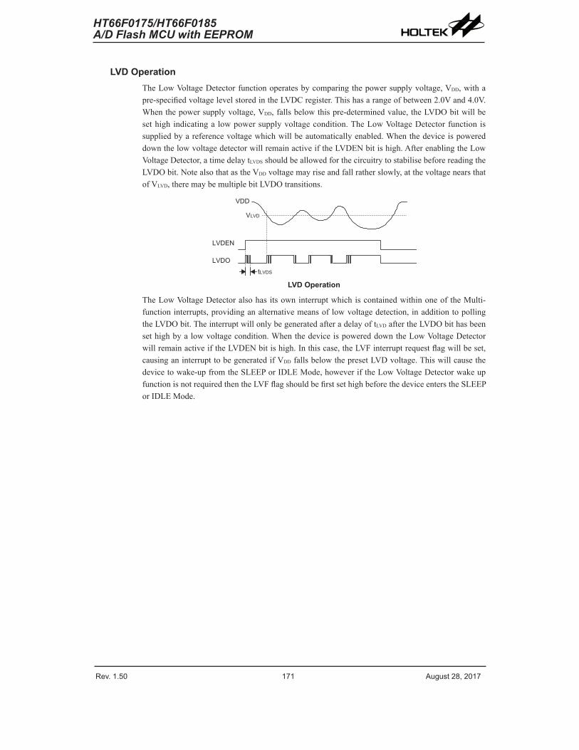
Rev. 1.50 1�0 ����st ��� �01� Rev. 1.50 1�1 ����st ��� �01�
HT66F0175/HT66F0185A/D Flash MCU with EEPROM
HT66F0175/HT66F0185A/D Flash MCU with EEPROM
LVD OperationTheLowVoltageDetectorfunctionoperatesbycomparingthepowersupplyvoltage,VDD,withapre-specifiedvoltagelevelstoredintheLVDCregister.Thishasarangeofbetween2.0Vand4.0V.Whenthepowersupplyvoltage,VDD,fallsbelowthispre-determinedvalue,theLVDObitwillbesethighindicatinga lowpowersupplyvoltagecondition.TheLowVoltageDetectorfunctionissuppliedbyareferencevoltagewhichwillbeautomaticallyenabled.WhenthedeviceispowereddownthelowvoltagedetectorwillremainactiveiftheLVDENbitishigh.AfterenablingtheLowVoltageDetector,atimedelaytLVDSshouldbeallowedforthecircuitrytostabilisebeforereadingtheLVDObit.NotealsothatastheVDDvoltagemayriseandfallratherslowly,atthevoltagenearsthatofVLVD,theremaybemultiplebitLVDOtransitions.
� � �
� � � �
� � � � �
� � � �� � � � �
LVD Operation
TheLowVoltageDetectoralsohasitsowninterruptwhichiscontainedwithinoneoftheMulti-functioninterrupts,providinganalternativemeansoflowvoltagedetection,inadditiontopollingtheLVDObit.TheinterruptwillonlybegeneratedafteradelayoftLVDaftertheLVDObithasbeensethighbyalowvoltagecondition.WhenthedeviceispowereddowntheLowVoltageDetectorwillremainactiveiftheLVDENbitishigh.Inthiscase,theLVFinterruptrequestflagwillbeset,causinganinterrupttobegeneratedifVDDfallsbelowthepresetLVDvoltage.Thiswillcausethedevicetowake-upfromtheSLEEPorIDLEMode,howeveriftheLowVoltageDetectorwakeupfunctionisnotrequiredthentheLVFflagshouldbefirstsethighbeforethedeviceenterstheSLEEPorIDLEMode.

Rev. 1.50 1�� ����st ��� �01� Rev. 1.50 1�3 ����st ��� �01�
HT66F0175/HT66F0185A/D Flash MCU with EEPROM
HT66F0175/HT66F0185A/D Flash MCU with EEPROM
InterruptsInterruptsarean importantpartofanymicrocontroller system.WhenanexternaleventoraninternalfunctionsuchasaTimerModuleoranA/Dconverterrequiresmicrocontrollerattention,theircorrespondinginterruptwillenforceatemporarysuspensionofthemainprogramallowingthemicrocontrollertodirectattentiontotheirrespectiveneeds.Thesedevicescontainseveralexternalinterruptandinternal interruptsfunctions.Theexternal interruptsaregeneratedbytheactionoftheexternalINT0andINT1pins,while the internal interruptsaregeneratedbyvarious internalfunctionssuchastheTMs,TimeBase,LVD,EEPROM,SIM,UARTandtheA/Dconverter,etc.
Interrupt RegistersOverall interrupt control,whichbasicallymeans the settingof request flagswhen certainmicrocontrollerconditionsoccurandthesettingofinterruptenablebitsbytheapplicationprogram,iscontrolledbyaseriesofregisters,locatedintheSpecialPurposeDataMemory,asshownintheaccompanyingtable.Thenumberofregistersdependsuponthedevicechosenbutfall intothreecategories.ThefirstistheINTC0~INTC2registerswhichsetuptheprimaryinterrupts,thesecondistheMFI0~MFI2registerswhichsetuptheMulti-functioninterrupts.FinallythereisanINTEGregistertosetuptheexternalinterrupttriggeredgetype.
Eachregistercontainsanumberofenablebits toenableordisable individual interruptsaswellasinterruptflagstoindicatethepresenceofaninterruptrequest.Thenamingconventionofthesefollowsaspecificpattern.Firstislistedanabbreviatedinterrupttype,thenthe(optional)numberofthatinterruptfollowedbyeitheran“E”forenable/disablebitor“F”forrequestflag.
Function Enable Bit Request Flag NotesGlobal EMI — —INTn Pins INTnE INTnF n = 0 ~ 1M�lti-f�nction MFnE MFnF n = 0~��/D Converter �DE �DF —Time Base TBnE TBnF n = 0 ~ 1SIM SIME SIMF —LVD LVE LVF —EEPROM write operation DEE DEF —
TMTnPE TnPF n = 0~1Tn�E Tn�F n = 0~1
Interrupt Register Bit Naming Conventions – HT66F0175
Function Enable Bit Request Flag NotesGlobal EMI — —INTn Pins INTnE INTnF n = 0 ~ 1Comparator CPE CPF —M�lti-f�nction MFnE MFnF n = 0~��/D Converter �DE �DF —Time Base TBnE TBnF n = 0 ~ 1SIM SIME SIMF —U�RT URE URF —LVD LVE LVF —EEPROM write operation DEE DEF —
TMTnPE TnPF n = 0~�Tn�E Tn�F n = 0~�
Interrupt Register Bit Naming Conventions – HT66F0185
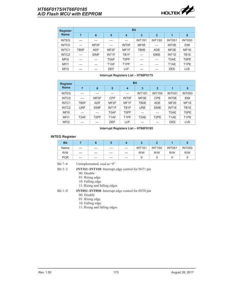
Rev. 1.50 1�� ����st ��� �01� Rev. 1.50 1�3 ����st ��� �01�
HT66F0175/HT66F0185A/D Flash MCU with EEPROM
HT66F0175/HT66F0185A/D Flash MCU with EEPROM
Register Name
Bit
7 6 5 4 3 2 1 0INTEG — — — — INT1S1 INT1S0 INT0S1 INT0S0INTC0 — MF0F — INT0F MF0E — INT0E EMIINTC1 TB0F �DF MF�F MF1F TB0E �DE MF�E MF1EINTC� — SIMF INT1F TB1F — SIME INT1E TB1EMFI0 — — T0�F T0PF — — T0�E T0PEMFI1 — — T1�F T1PF — — T1�E T1PEMFI� — — DEF LVF — — DEE LVE
Interrupt Registers List – HT66F0175
Register Name
Bit
7 6 5 4 3 2 1 0INTEG — — — — INT1S1 INT1S0 INT0S1 INT0S0INTC0 — MF0F CPF INT0F MF0E CPE INT0E EMIINTC1 TB0F �DF MF�F MF1F TB0E �DE MF�E MF1EINTC� URF SIMF INT1F TB1F URE SIME INT1E TB1EMFI0 — — T0�F T0PF — — T0�E T0PEMFI1 T��F T�PF T1�F T1PF T��E T�PE T1�E T1PEMFI� — — DEF LVF — — DEE LVE
Interrupt Registers List – HT66F0185
INTEG Register
Bit 7 6 5 4 3 2 1 0Name — — — — INT1S1 INT1S0 INT0S1 INT0S0R/W — — — — R/W R/W R/W R/WPOR — — — — 0 0 0 0
Bit7~4 Unimplemented,readas“0”Bit3~2 INT1S1~INT1S0:InterruptedgecontrolforINT1pin
00:Disable01:Risingedge10:Fallingedge11:Risingandfallingedges
Bit1~0 INT0S1~INT0S0:InterruptedgecontrolforINT0pin00:Disable01:Risingedge10:Fallingedge11:Risingandfallingedges

Rev. 1.50 1�4 ����st ��� �01� Rev. 1.50 1�5 ����st ��� �01�
HT66F0175/HT66F0185A/D Flash MCU with EEPROM
HT66F0175/HT66F0185A/D Flash MCU with EEPROM
INTC0 Register – HT66F0175
Bit 7 6 5 4 3 2 1 0Name — MF0F — INT0F MF0E — INT0E EMIR/W — R/W — R/W R/W — R/W R/WPOR — 0 — 0 0 — 0 0
Bit7 Unimplemented,readas“0”Bit6 MF0F:Multi-function0interruptrequestflag
0:Norequest1:Interruptrequest
Bit5 Unimplemented,readas“0”Bit4 INT0F:INT0interruptrequestflag
0:Norequest1:Interruptrequest
Bit3 MF0E:Multi-function0interruptcontrol0:Disable1:Enable
Bit2 Unimplemented,readas“0”Bit1 INT0E:INT0interruptcontrol
0:Disable1:Enable
Bit0 EMI:Globalinterruptcontrol0:Disable1:Enable
INTC0 Register – HT66F0185
Bit 7 6 5 4 3 2 1 0Name — MF0F CPF INT0F MF0E CPE INT0E EMIR/W — R/W R/W R/W R/W R/W R/W R/WPOR — 0 0 0 0 0 0 0
Bit7 Unimplemented,readas“0”Bit6 MF0F:Multi-function0interruptrequestflag
0:Norequest1:Interruptrequest
Bit5 CPF:Comparatorinterruptrequestflag0:Norequest1:Interruptrequest
Bit4 INT0F:INT0interruptrequestflag0:norequest1:interruptrequest
Bit3 MF0E:Multi-function0interruptcontrol0:Disable1:Enable
Bit2 CPE:Comparatorinterruptcontrol0:Disable1:Enable
Bit1 INT0E:INT0interruptcontrol0:Disable1:Enable
Bit0 EMI:Globalinterruptcontrol0:Disable1:Enable
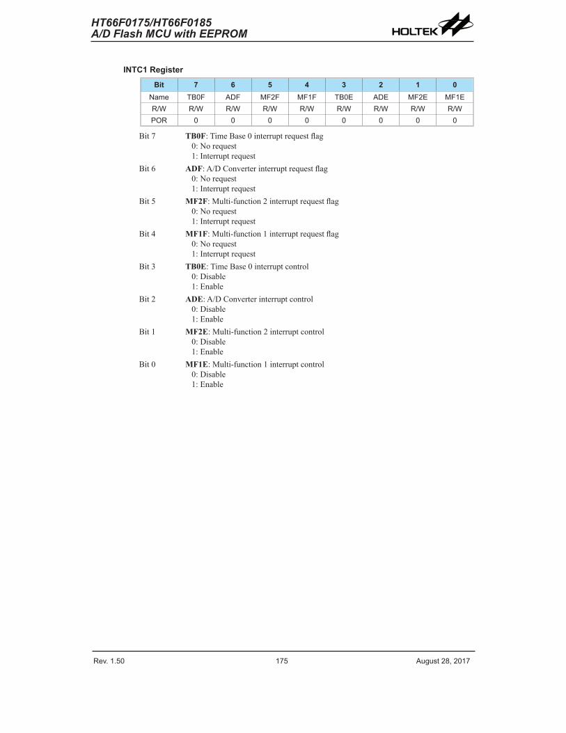
Rev. 1.50 1�4 ����st ��� �01� Rev. 1.50 1�5 ����st ��� �01�
HT66F0175/HT66F0185A/D Flash MCU with EEPROM
HT66F0175/HT66F0185A/D Flash MCU with EEPROM
INTC1 Register
Bit 7 6 5 4 3 2 1 0Name TB0F �DF MF�F MF1F TB0E �DE MF�E MF1ER/W R/W R/W R/W R/W R/W R/W R/W R/WPOR 0 0 0 0 0 0 0 0
Bit7 TB0F:TimeBase0interruptrequestflag0:Norequest1:Interruptrequest
Bit6 ADF:A/DConverterinterruptrequestflag0:Norequest1:Interruptrequest
Bit5 MF2F:Multi-function2interruptrequestflag0:Norequest1:Interruptrequest
Bit4 MF1F:Multi-function1interruptrequestflag0:Norequest1:Interruptrequest
Bit3 TB0E:TimeBase0interruptcontrol0:Disable1:Enable
Bit2 ADE:A/DConverterinterruptcontrol0:Disable1:Enable
Bit1 MF2E:Multi-function2interruptcontrol0:Disable1:Enable
Bit0 MF1E:Multi-function1interruptcontrol0:Disable1:Enable

Rev. 1.50 1�6 ����st ��� �01� Rev. 1.50 1�� ����st ��� �01�
HT66F0175/HT66F0185A/D Flash MCU with EEPROM
HT66F0175/HT66F0185A/D Flash MCU with EEPROM
INTC2 Register – HT66F0175
Bit 7 6 5 4 3 2 1 0Name — SIMF INT1F TB1F — SIME INT1E TB1ER/W — R/W R/W R/W — R/W R/W R/WPOR — 0 0 0 — 0 0 0
Bit7 Unimplemented,readas“0”Bit6 SIMF:SIMinterruptrequestflag
0:Norequest1:Interruptrequest
Bit5 INT1F:INT1interruptrequestflag0:Norequest1:Interruptrequest
Bit4 TB1F:TimeBase1interruptrequestflag0:Norequest1:Interruptrequest
Bit3 Unimplemented,readas“0”Bit2 SIME:SIMinterruptcontrol
0:Disable1:Enable
Bit1 INT1E:INT1interruptcontrol0:Disable1:Enable
Bit0 TB1E:TimeBase1interruptcontrol0:Disable1:Enable
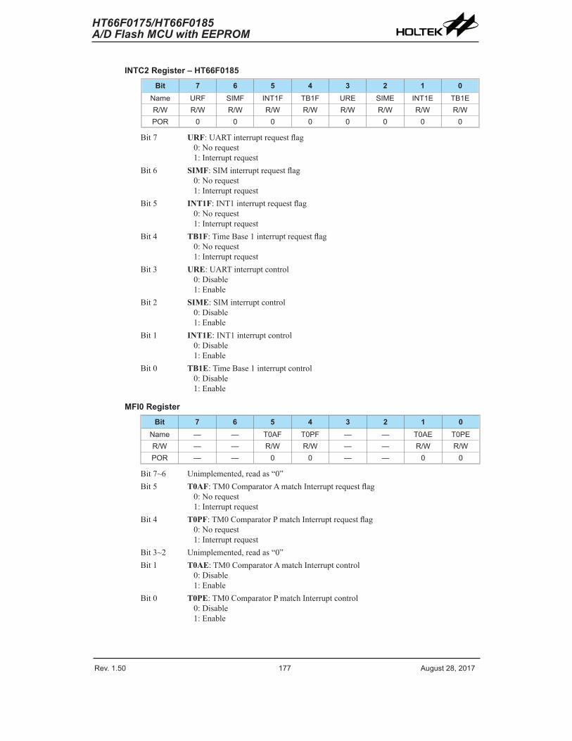
Rev. 1.50 1�6 ����st ��� �01� Rev. 1.50 1�� ����st ��� �01�
HT66F0175/HT66F0185A/D Flash MCU with EEPROM
HT66F0175/HT66F0185A/D Flash MCU with EEPROM
INTC2 Register – HT66F0185
Bit 7 6 5 4 3 2 1 0Name URF SIMF INT1F TB1F URE SIME INT1E TB1ER/W R/W R/W R/W R/W R/W R/W R/W R/WPOR 0 0 0 0 0 0 0 0
Bit7 URF:UARTinterruptrequestflag0:Norequest1:Interruptrequest
Bit6 SIMF:SIMinterruptrequestflag0:Norequest1:Interruptrequest
Bit5 INT1F:INT1interruptrequestflag0:Norequest1:Interruptrequest
Bit4 TB1F:TimeBase1interruptrequestflag0:Norequest1:Interruptrequest
Bit3 URE:UARTinterruptcontrol0:Disable1:Enable
Bit2 SIME:SIMinterruptcontrol0:Disable1:Enable
Bit1 INT1E:INT1interruptcontrol0:Disable1:Enable
Bit0 TB1E:TimeBase1interruptcontrol0:Disable1:Enable
MFI0 Register
Bit 7 6 5 4 3 2 1 0Name — — T0�F T0PF — — T0�E T0PER/W — — R/W R/W — — R/W R/WPOR — — 0 0 — — 0 0
Bit7~6 Unimplemented,readas“0”Bit5 T0AF:TM0ComparatorAmatchInterruptrequestflag
0:Norequest1:Interruptrequest
Bit4 T0PF:TM0ComparatorPmatchInterruptrequestflag0:Norequest1:Interruptrequest
Bit3~2 Unimplemented,readas“0”Bit1 T0AE:TM0ComparatorAmatchInterruptcontrol
0:Disable1:Enable
Bit0 T0PE:TM0ComparatorPmatchInterruptcontrol0:Disable1:Enable

Rev. 1.50 1�� ����st ��� �01� Rev. 1.50 1�9 ����st ��� �01�
HT66F0175/HT66F0185A/D Flash MCU with EEPROM
HT66F0175/HT66F0185A/D Flash MCU with EEPROM
MFI1 Register – HT66F0175
Bit 7 6 5 4 3 2 1 0Name — — T1�F T1PF — — T1�E T1PER/W — — R/W R/W — — R/W R/WPOR — — 0 0 — — 0 0
Bit7~6 Unimplemented,readas“0”Bit5 T1AF:TM1ComparatorAmatchInterruptrequestflag
0:Norequest1:Interruptrequest
Bit4 T1PF:TM1ComparatorPmatchInterruptrequestflag0:Norequest1:Interruptrequest
Bit3~2 Unimplemented,readas“0”Bit1 T1AE:TM1ComparatorAmatchInterruptcontrol
0:Disable1:Enable
Bit0 T1PE:TM1ComparatorPmatchInterruptcontrol0:Disable1:Enable
MFI1 Register – HT66F0185
Bit 7 6 5 4 3 2 1 0Name T��F T�PF T1�F T1PF T��E T�PE T1�E T1PER/W R/W R/W R/W R/W R/W R/W R/W R/WPOR 0 0 0 0 0 0 0 0
Bit7 T2AF:TM2ComparatorAmatchInterruptrequestflag0:Norequest1:Interruptrequest
Bit6 T2PF:TM2ComparatorPmatchInterruptrequestflag0:Norequest1:Interruptrequest
Bit5 T1AF:TM1ComparatorAmatchInterruptrequestflag0:Norequest1:Interruptrequest
Bit4 T1PF:TM1ComparatorPmatchInterruptrequestflag0:Norequest1:Interruptrequest
Bit3 T2AE:TM2ComparatorAmatchInterruptcontrol0:Disable1:Enable
Bit2 T2PE:TM2ComparatorPmatchInterruptcontrol0:Disable1:Enable
Bit1 T1AE:TM1ComparatorAmatchInterruptcontrol0:Disable1:Enable
Bit0 T1PE:TM1ComparatorPmatchInterruptcontrol0:Disable1:Enable

Rev. 1.50 1�� ����st ��� �01� Rev. 1.50 1�9 ����st ��� �01�
HT66F0175/HT66F0185A/D Flash MCU with EEPROM
HT66F0175/HT66F0185A/D Flash MCU with EEPROM
MFI2 Register
Bit 7 6 5 4 3 2 1 0Name — — DEF LVF — — DEE LVER/W — — R/W R/W — — R/W R/WPOR — — 0 0 — — 0 0
Bit7~6 Unimplemented,readas“0”Bit5 DEF:DataEEPROMInterruptrequestflag
0:Norequest1:Interruptrequest
Bit4 LVF:LVDInterruptrequestflag0:Norequest1:Interruptrequest
Bit3~2 Unimplemented,readas“0”Bit1 DEE:DataEEPROMInterruptcontrol
0:Disable1:Enable
Bit0 LVE:LVDInterruptcontrol0:Disable1:Enable
Interrupt OperationWhentheconditionsforaninterrupteventoccur,suchasaTMComparatorPorComparatorAorA/Dconversioncompletion,etc,therelevantinterruptrequestflagwillbeset.Whethertherequestflagactuallygeneratesaprogramjumptotherelevantinterruptvectorisdeterminedbytheconditionoftheinterruptenablebit.Iftheenablebitissethighthentheprogramwilljumptoitsrelevantvector;iftheenablebitiszerothenalthoughtheinterruptrequestflagissetanactualinterruptwillnotbegeneratedandtheprogramwillnotjumptotherelevantinterruptvector.Theglobalinterruptenablebit,ifclearedtozero,willdisableallinterrupts.
Whenaninterruptisgenerated,theProgramCounter,whichstorestheaddressofthenextinstructiontobeexecuted,willbetransferredontothestack.TheProgramCounterwillthenbeloadedwithanewaddresswhichwillbethevalueofthecorrespondinginterruptvector.Themicrocontrollerwillthenfetchitsnextinstructionfromthisinterruptvector.TheinstructionatthisvectorwillusuallybeaJMPwhichwill jumptoanothersectionofprogramwhichisknownastheinterruptserviceroutine.Hereislocatedthecodetocontroltheappropriateinterrupt.TheinterruptserviceroutinemustbeterminatedwithaRETI,whichretrievestheoriginalProgramCounteraddressfromthestackandallows themicrocontroller tocontinuewithnormalexecutionat thepointwhere theinterruptoccurred.
Thevarious interruptenablebits, togetherwith theirassociatedrequest flags,areshownin theaccompanyingdiagramswith theirorderofpriority.Some interrupt sourceshave theirownindividualvectorwhileothersshare thesamemulti-function interruptvector.Oncean interruptsubroutineisserviced,allotherinterruptswillbeblocked,astheglobalinterruptenablebit,EMIbitwillbeclearedautomatically.Thiswillpreventanyfurther interruptnestingfromoccurring.However, ifother interruptrequestsoccurduringthis interval,althoughtheinterruptwillnotbeimmediatelyserviced,therequestflagwillstillberecorded.

Rev. 1.50 1�0 ����st ��� �01� Rev. 1.50 1�1 ����st ��� �01�
HT66F0175/HT66F0185A/D Flash MCU with EEPROM
HT66F0175/HT66F0185A/D Flash MCU with EEPROM
Ifaninterruptrequiresimmediateservicingwhiletheprogramisalreadyinanotherinterruptserviceroutine,theEMIbitshouldbesetafterenteringtheroutinetoallowinterruptnesting.Ifthestackisfull,theinterruptrequestwillnotbeacknowledged,eveniftherelatedinterruptisenabled,untiltheStackPointerisdecremented.Ifimmediateserviceisdesired,thestackmustbepreventedfrombecomingfull.Incaseofsimultaneousrequests,theaccompanyingdiagramshowstheprioritythatisapplied.Alloftheinterruptrequestflagswhensetwillwake-upthedeviceifit isinSLEEPorIDLEMode,however topreventawake-upfromoccurringthecorrespondingflagshouldbesetbeforethedeviceisinSLEEPorIDLEMode.
INT0 Pin
INT1 Pin
INT0F
INT1F
INT0E
INT1E
EMI 04H
EMIM. F�nct. 0 MF0F MF0E
EMI
0CH
EMI
10H
14H
Time Base 0 TB0F TB0E
EMI 1�H
LVD LVF LVEEMI 1CH
Interr�pt Name
Req�est Fla�s
Enable Bits
Master Enable Vector
EMI a�to disabled in ISR
Priority
Hi�h
Low
M. F�nct. 1 MF1F MF1ETM0 P T0PF T0PE
TM0 � T0�F T0�E
Interr�pts contained within M�lti-F�nction Interr�pts
xxE Enable Bits
xxF Req�est Fla�� a�to reset in ISR
LegendxxF Req�est Fla�� no a�to reset in ISR
EMI �0H
�/D �DF �DE
EMI �4H
M. F�nct. � MF�F MF�E
Time Base 1 TB1F TB1E
TM1 P T1PE
TM1 � T1�E
EEPROM DEF DEE
SIM SIMF SIME EMI ��H
T1PF
T1�F
Interrupt Scheme – HT66F0175
INT0 Pin
INT1 Pin
INT0F
INT1F
INT0E
INT1E
EMI 04H
EMI
0�H
M. F�nct. 0 MF0F MF0E
EMI
0CH
EMI
10H
14H
Time Base 0 TB0F TB0E
EMI 1�H
LVD LVF LVE
EMI 1CH
Interr�pt Name
Req�est Fla�s
Enable Bits
Master Enable Vector
EMI a�to disabled in ISR
Priority
Hi�h
Low
M. F�nct. 1 MF1F MF1ETM0 P T0PF T0PE
TM0 � T0�F T0�E
Interr�pts contained within M�lti-F�nction Interr�pts
xxE Enable Bits
xxF Req�est Fla�� a�to reset in ISR
LegendxxF Req�est Fla�� no a�to reset in ISR
EMI �0H
�/D �DF �DE
EMI �4H
M. F�nct. � MF�F MF�E
Time Base 1 TB1F TB1E
TM1 P T1PE
TM1 � T1�E
EEPROM DEF DEE
TM� P T�PE
TM� � T��E
EMIComparator CPF CPE
SIM SIMF SIME EMI ��H
T1PF
T1�F
T�PF
T��F
U�RT URF URE EMI �CH
Interrupt Scheme – HT66F0185

Rev. 1.50 1�0 ����st ��� �01� Rev. 1.50 1�1 ����st ��� �01�
HT66F0175/HT66F0185A/D Flash MCU with EEPROM
HT66F0175/HT66F0185A/D Flash MCU with EEPROM
External InterruptTheexternal interruptsarecontrolledbysignal transitionsonthepinsINT0~INT1.Anexternalinterruptrequestwill takeplacewhentheexternalinterruptrequestflags,INT0F~INT1F,areset,whichwilloccurwhenatransition,whosetypeischosenbytheedgeselectbits,appearsontheexternal interruptpins.Toallowtheprogramtobranchtoitsrespectiveinterruptvectoraddress,theglobal interruptenablebit,EMI,andrespectiveexternal interruptenablebit, INT0E~INT1E,mustfirstbeset.Additionally thecorrect interruptedgetypemustbeselectedusingtheINTEGregistertoenabletheexternalinterruptfunctionandtochoosethetriggeredgetype.Astheexternalinterruptpinsarepin-sharedwithI/Opins,theycanonlybeconfiguredasexternalinterruptpinsiftheirexternalinterruptenablebitinthecorrespondinginterruptregisterhasbeensetandtheexternalinterruptpinisselectedbythecorrespondingpin-sharedfunctionselectionbits.Thepinmustalsobesetupasaninputbysettingthecorrespondingbitintheportcontrolregister.Whentheinterruptisenabled,thestackisnotfullandthecorrecttransitiontypeappearsontheexternalinterruptpin,asubroutinecalltotheexternalinterruptvector,willtakeplace.Whentheinterruptisserviced,theexternalinterruptrequestflags,INT0F~INT1F,willbeautomaticallyresetandtheEMIbitwillbeautomaticallyclearedtodisableotherinterrupts.Notethatanypull-highresistorselectionsontheexternalinterruptpinswillremainvalidevenifthepinisusedasanexternalinterruptinput.
TheINTEGregisterisusedtoselectthetypeofactiveedgethatwilltriggertheexternalinterrupt.Achoiceofeitherrisingorfallingorbothedgetypescanbechosentotriggeranexternalinterrupt.NotethattheINTEGregistercanalsobeusedtodisabletheexternalinterruptfunction.
Comparator Interrupt – HT66F0185Thecomparator interrupt iscontrolledbytheinternalcomparator.Acomparator interruptrequestwill takeplacewhenthecomparatorinterruptrequestflag,CPF,isset,asituationthatwilloccurwhenthecomparatoroutputchangesstate.Toallowtheprogramtobranchtoitsrespectiveinterruptvectoraddress,theglobalinterruptenablebit,EMI,andcomparatorinterruptenablebit,CPE,mustfirstbeset.Whentheinterruptisenabled,thestackisnotfullandthecomparatorinputsgenerateacomparatoroutputtransition,asubroutinecalltothecomparatorinterruptvector,willtakeplace.Whentheinterruptisserviced,thecomparatorinterruptrequestflag,willbeautomaticallyresetandtheEMIbitwillbeautomaticallyclearedtodisableotherinterrupts.
Multi-function InterruptWithin thedevice thereareup to threeMulti-function interrupts.Unlike theother independentinterrupts, theseinterruptshavenoindependentsource,butratherareformedfromotherexistinginterruptsources,namelytheTMinterrupts,LVDinterruptandEEPROMwriteoperationinterrupt.
AMulti-functioninterruptrequestwilltakeplacewhenanyoftheMulti-functioninterruptrequestflagsMFnFareset.TheMulti-function interrupt flagswillbesetwhenanyof their includedfunctionsgenerateaninterruptrequestflag.Toallowtheprogramtobranchtoitsrespectiveinterruptvectoraddress,whentheMulti-functioninterruptisenabledandthestackisnotfull,andeitheroneoftheinterruptscontainedwithineachofMulti-functioninterruptoccurs,asubroutinecalltooneoftheMulti-functioninterruptvectorswilltakeplace.Whentheinterruptisserviced,therelatedMulti-FunctionrequestflagwillbeautomaticallyresetandtheEMIbitwillbeautomaticallyclearedtodisableotherinterrupts.
However, itmustbenoted that, although theMulti-function Interrupt request flagswill beautomaticallyresetwhen the interrupt isserviced, therequest flagsfromtheoriginalsourceoftheMulti-function interruptswillnotbeautomaticallyresetandmustbemanuallyresetby theapplicationprogram.

Rev. 1.50 1�� ����st ��� �01� Rev. 1.50 1�3 ����st ��� �01�
HT66F0175/HT66F0185A/D Flash MCU with EEPROM
HT66F0175/HT66F0185A/D Flash MCU with EEPROM
A/D Converter InterruptTheA/DConverterInterruptiscontrolledbytheterminationofanA/Dconversionprocess.AnA/DConverterInterruptrequestwilltakeplacewhentheA/DConverterInterruptrequestflag,ADF,isset,whichoccurswhentheA/Dconversionprocessfinishes.Toallowtheprogramtobranchtoitsrespectiveinterruptvectoraddress,theglobalinterruptenablebit,EMI,andA/DInterruptenablebit,ADE,mustfirstbeset.Whentheinterruptisenabled,thestackisnotfullandtheA/Dconversionprocesshasended,asubroutinecalltotheA/DConverterInterruptvector,willtakeplace.Whentheinterruptisserviced,theA/DConverterInterruptflag,ADF,willbeautomaticallycleared.TheEMIbitwillalsobeautomaticallyclearedtodisableotherinterrupts.
Time Base InterruptThefunctionoftheTimeBaseInterruptsistoprovideregulartimesignalintheformofaninternalinterrupt.Theyarecontrolledbytheoverflowsignalsfromtheirrespectivetimerfunctions.Whenthesehappens their respective interrupt request flags,TB0ForTB1Fwillbeset.Toallowtheprogramtobranchtotheirrespectiveinterruptvectoraddresses,theglobalinterruptenablebit,EMIandTimeBaseenablebits,TB0EorTB1E,mustfirstbeset.Whentheinterruptisenabled,thestackisnotfullandtheTimeBaseoverflows,asubroutinecall totheirrespectivevectorlocationswilltakeplace.Whentheinterruptisserviced,therespectiveinterruptrequestflag,TB0ForTB1F,willbeautomaticallyresetandtheEMIbitwillbeclearedtodisableotherinterrupts.ThepurposeoftheTimeBaseInterruptistoprovideaninterruptsignalatfixedtimeperiods.Theirclocksourcesoriginate fromthe internalclocksource fTB.This fTB inputclockpasses throughadivider, thedivisionratioofwhichisselectedbyprogrammingtheappropriatebitsintheTBCregistertoobtainlonger interruptperiodswhosevalueranges.Theclocksource thatgenerates fTB,which in turncontrolstheTimeBaseinterruptperiod,canoriginatefromseveraldifferentsources,asshownintheSystemOperatingModesection.
MUXfSYS/4
fTBC
Prescaler
TBCK
fTB
fTB/�� ~ fTB/�15MUX
TB11~TB10
Time Base 0 Interr�pt
Time Base 1 Interr�pt
TB0�~TB00
PrescalerMUX
fTB/�1� ~ fTB/�15
Time Base Interrupts

Rev. 1.50 1�� ����st ��� �01� Rev. 1.50 1�3 ����st ��� �01�
HT66F0175/HT66F0185A/D Flash MCU with EEPROM
HT66F0175/HT66F0185A/D Flash MCU with EEPROM
TBC Register
Bit 7 6 5 4 3 2 1 0Name TBON TBCK TB11 TB10 LXTLP TB0� TB01 TB00R/W R/W R/W R/W R/W R/W R/W R/W R/WPOR 0 0 1 1 0 1 1 1
Bit7 TBON:TimeBasefunctionenablecontrol0:Disable1:Enable
Bit6 TBCK:TimeBaseclocksourceselect0:fTBC1:fSYS/4
Bit5~4 TB11~TB10:TimeBase1time-outperiodselection00:212/fTB01:213/fTB10:214/fTB11:215/fTB
Bit3 LXTLP:LXTLowPowercontrol0:Disable–LXTquickstart-up1:Enable–LXTslowstart-up
Bit2~0 TB02~TB00:TimeBase0time-outperiodselection000:28/fTB001:29/fTB010:210/fTB011:211/fTB100:212/fTB101:213/fTB110:214/fTB111:215/fTB
Serial Interface Module InterruptTheSerialInterfaceModuleInterrupt,alsoknownastheSIMinterrupt,iscontrolledbytheSPIorI2Cdatatransfer.ASIMInterruptrequestwilltakeplacewhentheSIMInterruptrequestflag,SIMF,isset,whichoccurswhenabyteofdatahasbeenreceivedor transmittedbytheSIMinterface,anI2CslaveaddressmatchorI2Cbustime-outoccurrence.Toallowtheprogramtobranchtoitsrespective interruptvectoraddress, theglobal interruptenablebit,EMIandtheSerial InterfaceInterruptenablebit,SIME,mustfirstbeset.Whentheinterruptisenabled,thestackisnotfullandanyoftheabovedescribedsituationsoccurs,asubroutinecalltotherespectiveSIMInterruptvector,will takeplace.WhentheSerialInterfaceInterruptisserviced,theEMIbitwillbeautomaticallyclearedtodisableotherinterrupts.TheSIMFflagwillalsobeautomaticallycleared.
UART Transfer Interrupt – HT66F0185TheUARTTransferInterruptiscontrolledbyseveralUARTtransferconditions.Whenoneoftheseconditionsoccurs,aninterruptpulsewillbegeneratedtoget theattentionof themicrocontroller.Theseconditionsarea transmitterdata registerempty, transmitter idle, receiverdataavailable,receiveroverrun,addressdetectandanRXpinwake-up.Toallowtheprogramtobranchto itsrespective interruptvectoraddress, theglobal interruptenablebit,EMI,andUARTInterruptenablebit,URE,mustfirstbeset.Whentheinterruptisenabled,thestackisnotfullandanyoftheconditionsdescribedaboveoccurs,asubroutinecalltotheUARTInterruptvector,willtakeplace.Whentheinterruptisserviced, theUARTInterruptflag,URF,willbeautomaticallycleared.TheEMIbitwillalsobeautomaticallyclearedtodisableotherinterrupts.

Rev. 1.50 1�4 ����st ��� �01� Rev. 1.50 1�5 ����st ��� �01�
HT66F0175/HT66F0185A/D Flash MCU with EEPROM
HT66F0175/HT66F0185A/D Flash MCU with EEPROM
LVD InterruptTheLowVoltageDetector Interrupt iscontainedwithin theMulti-function Interrupt.AnLVDInterruptrequestwill takeplacewhentheLVDInterruptrequestflag,LVF, isset,whichoccurswhentheLowVoltageDetectorfunctiondetectsalowpowersupplyvoltage.Toallowtheprogramtobranchtoitsrespectiveinterruptvectoraddress,theglobalinterruptenablebit,EMI,LowVoltageInterruptenablebit,LVE,andassociatedMulti-functioninterruptenablebit,mustfirstbeset.Whentheinterruptisenabled,thestackisnotfullandalowvoltageconditionoccurs,asubroutinecalltotheMulti-functionInterruptvector,willtakeplace.WhentheLowVoltageInterruptisserviced,theEMIbitwillbeautomaticallyclearedtodisableotherinterrupts.However,onlytheMulti-functioninterruptrequestflagwillbealsoautomaticallycleared.AstheLVFflagwillnotbeautomaticallycleared,ithastobeclearedbytheapplicationprogram.
EEPROM InterruptTheEEPROMWrite Interrupt iscontainedwithin theMulti-function Interrupt.AnEEPROMWriteInterruptrequestwilltakeplacewhentheEEPROMWriteInterruptrequestflag,DEF,isset,whichoccurswhenanEEPROMWritecycleends.Toallowtheprogramtobranchtoitsrespectiveinterruptvectoraddress,theglobalinterruptenablebit,EMI,EEPROMWriteInterruptenablebit,DEE,andassociatedMulti-function interruptenablebitmustfirstbeset.Whenthe interrupt isenabled,thestackisnotfullandanEEPROMWritecycleends,asubroutinecalltotherespectiveMulti-functionInterruptvectorwilltakeplace.WhentheEEPROMWriteInterruptisserviced,theEMIbitwillbeautomaticallyclearedtodisableotherinterrupts.However,onlytheMulti-functioninterrupt request flagwillbeautomaticallycleared.As theDEFflagwillnotbeautomaticallycleared,ithastobeclearedbytheapplicationprogram.
TM InterruptTheCompact,StandardandPeriodicTMshavetwointerrupts,onecomesfromthecomparatorAmatchsituationandtheothercomesfromthecomparatorPmatchsituation.AlloftheTMinterruptsarecontainedwithintheMulti-functionInterrupts.ForalloftheTMtypestherearetwointerruptrequestflagsandtwoenablecontrolbits.ATMinterruptrequestwill takeplacewhenanyoftheTMrequestflagsareset,asituationwhichoccurswhenaTMcomparatorPorAmatchsituationhappens.
Toallowtheprogramtobranchtoitsrespectiveinterruptvectoraddress,theglobalinterruptenablebit,EMI,respectiveTMInterruptenablebit,andrelevantMulti-functionInterruptenablebit,MFnE,mustfirstbeset.Whentheinterruptisenabled,thestackisnotfullandaTMcomparatormatchsituationoccurs,asubroutinecalltotherelevantMulti-functionInterruptvectorlocations,willtakeplace.WhentheTMinterruptisserviced,theEMIbitwillbeautomaticallyclearedtodisableotherinterrupts.However,onlytherelatedMFnFflagwillbeautomaticallycleared.AstheTMinterruptrequestflagswillnotbeautomaticallycleared,theyhavetobeclearedbytheapplicationprogram.

Rev. 1.50 1�4 ����st ��� �01� Rev. 1.50 1�5 ����st ��� �01�
HT66F0175/HT66F0185A/D Flash MCU with EEPROM
HT66F0175/HT66F0185A/D Flash MCU with EEPROM
Interrupt Wake-up FunctionEachof the interruptfunctionshas thecapabilityofwakingupthemicrocontrollerwhenin theSLEEPorIDLEMode.Awake-upisgeneratedwhenaninterruptrequestflagchangesfromlowtohighandisindependentofwhethertheinterruptisenabledornot.Therefore,eventhoughthesedevicesare in theSLEEPor IDLEModeand its systemoscillatorstopped,situationssuchasexternaledgetransitionsontheexternalinterruptpins,alowpowersupplyvoltageorcomparatorinputchangemaycause theirrespectiveinterruptflag tobesethighandconsequentlygenerateaninterrupt.Caremustthereforebetakenifspuriouswake-upsituationsaretobeavoided.Ifaninterruptwake-upfunctionistobedisabledthenthecorrespondinginterruptrequestflagshouldbesethighbeforethedeviceenterstheSLEEPorIDLEMode.Theinterruptenablebitshavenoeffectontheinterruptwake-upfunction.
Programming ConsiderationsBydisablingtherelevantinterruptenablebits,arequestedinterruptcanbepreventedfrombeingserviced,however,oncean interrupt request flag is set, itwill remain in thiscondition in theinterruptregisteruntilthecorrespondinginterruptisservicedoruntiltherequestflagisclearedbytheapplicationprogram.
Whereacertain interrupt iscontainedwithinaMulti-function interrupt, thenwhenthe interruptservice routine isexecuted,asonly theMulti-function interrupt request flags,MFnF,willbeautomaticallycleared, the individual request flag for the functionneeds tobeclearedby theapplicationprogram.
It isrecommendedthatprogramsdonotusethe“CALL”instructionwithintheinterruptservicesubroutine.Interruptsoftenoccurinanunpredictablemannerorneedtobeservicedimmediately.Ifonlyonestackisleftandtheinterruptisnotwellcontrolled,theoriginalcontrolsequencewillbedamagedonceaCALLsubroutineisexecutedintheinterruptsubroutine.
EveryinterrupthasthecapabilityofwakingupthemicrocontrollerwhenitisintheSLEEPorIDLEMode,thewakeupbeinggeneratedwhentheinterruptrequestflagchangesfromlowtohigh.IfitisrequiredtopreventacertaininterruptfromwakingupthemicrocontrollerthenitsrespectiverequestflagshouldbefirstsethighbeforeenterSLEEPorIDLEMode.
AsonlytheProgramCounter ispushedontothestack, thenwhentheinterrupt isserviced, if thecontentsof theaccumulator,statusregisterorotherregistersarealteredbythe interruptserviceprogram,theircontentsshouldbesavedto thememoryat thebeginningof the interruptserviceroutine.
Toreturnfromaninterruptsubroutine,eitheraRETorRETIinstructionmaybeexecuted.TheRETIinstructioninadditiontoexecutingareturntothemainprogramalsoautomaticallysetstheEMIbithightoallowfurtherinterrupts.TheRETinstructionhoweveronlyexecutesareturntothemainprogramleavingtheEMIbitinitspresentzerostateandthereforedisablingtheexecutionoffurtherinterrupts.

Rev. 1.50 1�6 ����st ��� �01� Rev. 1.50 1�� ����st ��� �01�
HT66F0175/HT66F0185A/D Flash MCU with EEPROM
HT66F0175/HT66F0185A/D Flash MCU with EEPROM
Configuration OptionsConfigurationoptionsrefertocertainoptionswithintheMCUthatareprogrammedintothedeviceduringtheprogrammingprocess.Duringthedevelopmentprocess,theseoptionsareselectedusingtheHT-IDEsoftwaredevelopment tools.Astheseoptionsareprogrammedintothedeviceusingthehardwareprogrammingtools,once theyareselectedtheycannotbechangedlaterusingtheapplicationprogram.Alloptionsmustbedefinedforpropersystemfunction,thedetailsofwhichareshowninthetable.
No. Options
1 Hi�h Speed System Oscillator SelectionfH – HXT or HIRC
� Low Speed System Oscillator SelectionfSUB – LXT or LIRC
3 HIRC Freq�ency SelectionfHIRC – �MHz� 1�MHz or 16MHz
Application Circuits
VDD
VSS
VDD
PC0/OSC1PC1/OSC�
OSC Circ�it
PB0/XT1PB1/XT�
OSC Circ�it
See Oscillator Section
See Oscillator Section
�N0~�N�
SCOMn
SSEGmLCD
Panel
P�0~P��
PB0~PB6
PC0~PC6
PD0~PD3
0.1µF

Rev. 1.50 1�6 ����st ��� �01� Rev. 1.50 1�� ����st ��� �01�
HT66F0175/HT66F0185A/D Flash MCU with EEPROM
HT66F0175/HT66F0185A/D Flash MCU with EEPROM
Instruction Set
IntroductionCentral to thesuccessfuloperationofanymicrocontroller is its instructionset,whichisasetofprograminstructioncodesthatdirectsthemicrocontrollertoperformcertainoperations.InthecaseofHoltekmicrocontroller,acomprehensiveandflexiblesetofover60instructionsisprovidedtoenableprogrammerstoimplementtheirapplicationwiththeminimumofprogrammingoverheads.
Foreasierunderstandingofthevariousinstructioncodes, theyhavebeensubdividedintoseveralfunctionalgroupings.
Instruction TimingMostinstructionsareimplementedwithinoneinstructioncycle.Theexceptionstothisarebranch,call,or tablereadinstructionswheretwoinstructioncyclesarerequired.Oneinstructioncycleisequalto4systemclockcycles,thereforeinthecaseofan8MHzsystemoscillator,mostinstructionswouldbeimplementedwithin0.5μsandbranchorcall instructionswouldbeimplementedwithin1μs.Although instructionswhichrequireonemorecycle to implementaregenerally limited totheJMP,CALL,RET,RETIandtablereadinstructions, it is important torealize thatanyotherinstructionswhichinvolvemanipulationoftheProgramCounterLowregisterorPCLwillalsotakeonemorecycletoimplement.AsinstructionswhichchangethecontentsofthePCLwill implyadirect jumptothatnewaddress,onemorecyclewillberequired.Examplesofsuchinstructionswouldbe“CLRPCL”or“MOVPCL,A”.Forthecaseofskipinstructions,itmustbenotedthatiftheresultofthecomparisoninvolvesaskipoperationthenthiswillalsotakeonemorecycle,ifnoskipisinvolvedthenonlyonecycleisrequired.
Moving and Transferring DataThe transferofdatawithin themicrocontrollerprogram isoneof themost frequentlyusedoperations.MakinguseofseveralkindsofMOVinstructions,datacanbetransferredfromregisterstotheAccumulatorandvice-versaaswellasbeingabletomovespecificimmediatedatadirectlyintotheAccumulator.Oneofthemostimportantdatatransferapplicationsistoreceivedatafromtheinputportsandtransferdatatotheoutputports.
Arithmetic OperationsTheabilitytoperformcertainarithmeticoperationsanddatamanipulationisanecessaryfeatureofmostmicrocontrollerapplications.WithintheHoltekmicrocontrollerinstructionsetarearangeofaddandsubtract instructionmnemonicstoenablethenecessaryarithmetictobecarriedout.Caremustbe taken toensurecorrecthandlingofcarryandborrowdatawhenresultsexceed255foradditionandless than0forsubtraction.Theincrementanddecrement instructionssuchasINC,INCA,DECandDECAprovideasimplemeansofincreasingordecreasingbyavalueofoneofthevaluesinthedestinationspecified.

Rev. 1.50 1�� ����st ��� �01� Rev. 1.50 1�9 ����st ��� �01�
HT66F0175/HT66F0185A/D Flash MCU with EEPROM
HT66F0175/HT66F0185A/D Flash MCU with EEPROM
Logical and Rotate OperationThestandardlogicaloperationssuchasAND,OR,XORandCPLallhavetheirowninstructionwithintheHoltekmicrocontroller instructionset.Aswiththecaseofmost instructionsinvolvingdatamanipulation, datamust pass through theAccumulatorwhichmay involve additionalprogrammingsteps. Inall logicaldataoperations, thezero flagmaybeset if the resultof theoperationiszero.AnotherformoflogicaldatamanipulationcomesfromtherotateinstructionssuchasRR,RL,RRCandRLCwhichprovideasimplemeansofrotatingonebitrightorleft.Differentrotateinstructionsexistdependingonprogramrequirements.Rotateinstructionsareusefulforserialportprogrammingapplicationswheredatacanberotatedfromaninternalregister intotheCarrybitfromwhereitcanbeexaminedandthenecessaryserialbitsethighorlow.Anotherapplicationwhichrotatedataoperationsareusedistoimplementmultiplicationanddivisioncalculations.
Branches and Control TransferProgrambranchingtakestheformofeitherjumpstospecifiedlocationsusingtheJMPinstructionor toa subroutineusing theCALL instruction.Theydiffer in the sense that in thecaseofasubroutinecall, theprogrammustreturn to the instruction immediatelywhenthesubroutinehasbeencarriedout.Thisisdonebyplacingareturninstruction“RET”inthesubroutinewhichwillcausetheprogramtojumpbacktotheaddressrightaftertheCALLinstruction.InthecaseofaJMPinstruction,theprogramsimplyjumpstothedesiredlocation.ThereisnorequirementtojumpbacktotheoriginaljumpingoffpointasinthecaseoftheCALLinstruction.Onespecialandextremelyusefulsetofbranchinstructionsaretheconditionalbranches.Hereadecisionisfirstmaderegardingtheconditionofacertaindatamemoryor individualbits.Dependingupon theconditions, theprogramwillcontinuewiththenextinstructionorskipoveritandjumptothefollowinginstruction.These instructionsare thekey todecisionmakingandbranchingwithin theprogramperhapsdeterminedbytheconditionofcertaininputswitchesorbytheconditionofinternaldatabits.
Bit OperationsTheabilitytoprovidesinglebitoperationsonDataMemoryisanextremelyflexiblefeatureofallHoltekmicrocontrollers.Thisfeature isespeciallyusefulforoutputportbitprogrammingwhereindividualbitsorportpinscanbedirectlysethighorlowusingeitherthe“SET[m].i”or“CLR[m].i”instructionsrespectively.Thefeatureremovestheneedforprogrammerstofirstreadthe8-bitoutputport,manipulatetheinputdatatoensurethatotherbitsarenotchangedandthenoutputtheportwiththecorrectnewdata.Thisread-modify-writeprocessistakencareofautomaticallywhenthesebitoperationinstructionsareused.
Table Read OperationsDatastorage isnormally implementedbyusing registers.However,whenworkingwith largeamountsoffixeddata, thevolumeinvolvedoftenmakesit inconvenienttostorethefixeddataintheDataMemory.Toovercomethisproblem,HoltekmicrocontrollersallowanareaofProgramMemorytobesetupasatablewheredatacanbedirectlystored.Asetofeasytouseinstructionsprovides themeansbywhich this fixeddatacanbereferencedandretrievedfromtheProgramMemory.
Other OperationsInaddition to theabovefunctional instructions,a rangeofother instructionsalsoexistsuchasthe“HALT”instructionforPower-downoperationsand instructions tocontrol theoperationoftheWatchdogTimerfor reliableprogramoperationsunderextremeelectricorelectromagneticenvironments.Fortheirrelevantoperations,refertothefunctionalrelatedsections.
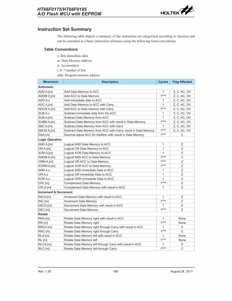
Rev. 1.50 1�� ����st ��� �01� Rev. 1.50 1�9 ����st ��� �01�
HT66F0175/HT66F0185A/D Flash MCU with EEPROM
HT66F0175/HT66F0185A/D Flash MCU with EEPROM
Instruction Set SummaryThefollowingtabledepictsasummaryoftheinstructionsetcategorisedaccordingtofunctionandcanbeconsultedasabasicinstructionreferenceusingthefollowinglistedconventions.
Table Conventionsx:Bitsimmediatedatam:DataMemoryaddressA:Accumulatori:0~7numberofbitsaddr:Programmemoryaddress
Mnemonic Description Cycles Flag AffectedArithmetic�DD ��[m] �dd Data Memory to �CC 1 Z� C� �C� OV�DDM ��[m] �dd �CC to Data Memory 1Note Z� C� �C� OV�DD ��x �dd immediate data to �CC 1 Z� C� �C� OV�DC ��[m] �dd Data Memory to �CC with Carry 1 Z� C� �C� OV�DCM ��[m] �dd �CC to Data memory with Carry 1Note Z� C� �C� OVSUB ��x S�btract immediate data from the �CC 1 Z� C� �C� OVSUB ��[m] S�btract Data Memory from �CC 1 Z� C� �C� OVSUBM ��[m] S�btract Data Memory from �CC with res�lt in Data Memory 1Note Z� C� �C� OVSBC ��[m] S�btract Data Memory from �CC with Carry 1 Z� C� �C� OVSBCM ��[m] S�btract Data Memory from �CC with Carry� res�lt in Data Memory 1Note Z� C� �C� OVD�� [m] Decimal adj�st �CC for �ddition with res�lt in Data Memory 1Note CLogic Operation�ND ��[m] Lo�ical �ND Data Memory to �CC 1 ZOR ��[m] Lo�ical OR Data Memory to �CC 1 ZXOR ��[m] Lo�ical XOR Data Memory to �CC 1 Z�NDM ��[m] Lo�ical �ND �CC to Data Memory 1Note ZORM ��[m] Lo�ical OR �CC to Data Memory 1Note ZXORM ��[m] Lo�ical XOR �CC to Data Memory 1Note Z�ND ��x Lo�ical �ND immediate Data to �CC 1 ZOR ��x Lo�ical OR immediate Data to �CC 1 ZXOR ��x Lo�ical XOR immediate Data to �CC 1 ZCPL [m] Complement Data Memory 1Note ZCPL� [m] Complement Data Memory with res�lt in �CC 1 ZIncrement & DecrementINC� [m] Increment Data Memory with res�lt in �CC 1 ZINC [m] Increment Data Memory 1Note ZDEC� [m] Decrement Data Memory with res�lt in �CC 1 ZDEC [m] Decrement Data Memory 1Note ZRotateRR� [m] Rotate Data Memory ri�ht with res�lt in �CC 1 NoneRR [m] Rotate Data Memory ri�ht 1Note NoneRRC� [m] Rotate Data Memory ri�ht thro��h Carry with res�lt in �CC 1 CRRC [m] Rotate Data Memory ri�ht thro��h Carry 1Note CRL� [m] Rotate Data Memory left with res�lt in �CC 1 NoneRL [m] Rotate Data Memory left 1Note NoneRLC� [m] Rotate Data Memory left thro��h Carry with res�lt in �CC 1 CRLC [m] Rotate Data Memory left thro��h Carry 1Note C

Rev. 1.50 190 ����st ��� �01� Rev. 1.50 191 ����st ��� �01�
HT66F0175/HT66F0185A/D Flash MCU with EEPROM
HT66F0175/HT66F0185A/D Flash MCU with EEPROM
Mnemonic Description Cycles Flag AffectedData MoveMOV ��[m] Move Data Memory to �CC 1 NoneMOV [m]�� Move �CC to Data Memory 1Note NoneMOV ��x Move immediate data to �CC 1 NoneBit OperationCLR [m].i Clear bit of Data Memory 1Note NoneSET [m].i Set bit of Data Memory 1Note NoneBranch OperationJMP addr J�mp �nconditionally � NoneSZ [m] Skip if Data Memory is zero 1Note NoneSZ� [m] Skip if Data Memory is zero with data movement to �CC 1Note NoneSZ [m].i Skip if bit i of Data Memory is zero 1Note NoneSNZ [m].i Skip if bit i of Data Memory is not zero 1Note NoneSIZ [m] Skip if increment Data Memory is zero 1Note NoneSDZ [m] Skip if decrement Data Memory is zero 1Note NoneSIZ� [m] Skip if increment Data Memory is zero with res�lt in �CC 1Note NoneSDZ� [m] Skip if decrement Data Memory is zero with res�lt in �CC 1Note NoneC�LL addr S�bro�tine call � NoneRET Ret�rn from s�bro�tine � NoneRET ��x Ret�rn from s�bro�tine and load immediate data to �CC � NoneRETI Ret�rn from interr�pt � NoneTable Read OperationT�BRD [m] Read table (specific page) to TBLH and Data Memory �Note NoneT�BRDC [m] Read table (c�rrent pa�e) to TBLH and Data Memory �Note NoneT�BRDL [m] Read table (last pa�e) to TBLH and Data Memory �Note NoneMiscellaneousNOP No operation 1 NoneCLR [m] Clear Data Memory 1Note NoneSET [m] Set Data Memory 1Note NoneCLR WDT Clear Watchdo� Timer 1 TO� PDFCLR WDT1 Pre-clear Watchdo� Timer 1 TO� PDFCLR WDT� Pre-clear Watchdo� Timer 1 TO� PDFSW�P [m] Swap nibbles of Data Memory 1Note NoneSW�P� [m] Swap nibbles of Data Memory with res�lt in �CC 1 NoneH�LT Enter power down mode 1 TO� PDF
Note:1.Forskipinstructions,iftheresultofthecomparisoninvolvesaskipthentwocyclesarerequired,ifnoskiptakesplaceonlyonecycleisrequired.
2.AnyinstructionwhichchangesthecontentsofthePCLwillalsorequire2cyclesforexecution.3.For the“CLRWDT1”and“CLRWDT2”instructionstheTOandPDFflagsmaybeaffectedbytheexecution status.TheTOandPDFflagsareclearedafterboth“CLRWDT1”and“CLRWDT2”instructionsareconsecutivelyexecuted.OtherwisetheTOandPDFflagsremainunchanged.

Rev. 1.50 190 ����st ��� �01� Rev. 1.50 191 ����st ��� �01�
HT66F0175/HT66F0185A/D Flash MCU with EEPROM
HT66F0175/HT66F0185A/D Flash MCU with EEPROM
Instruction Definition
ADC A,[m] AddDataMemorytoACCwithCarryDescription ThecontentsofthespecifiedDataMemory,Accumulatorandthecarryflagareadded. TheresultisstoredintheAccumulator.Operation ACC←ACC+[m]+CAffectedflag(s) OV,Z,AC,C
ADCM A,[m] AddACCtoDataMemorywithCarryDescription ThecontentsofthespecifiedDataMemory,Accumulatorandthecarryflagareadded. TheresultisstoredinthespecifiedDataMemory.Operation [m]←ACC+[m]+CAffectedflag(s) OV,Z,AC,C
ADD A,[m] AddDataMemorytoACCDescription ThecontentsofthespecifiedDataMemoryandtheAccumulatorareadded. TheresultisstoredintheAccumulator.Operation ACC←ACC+[m]Affectedflag(s) OV,Z,AC,C
ADD A,x AddimmediatedatatoACCDescription ThecontentsoftheAccumulatorandthespecifiedimmediatedataareadded. TheresultisstoredintheAccumulator.Operation ACC←ACC+xAffectedflag(s) OV,Z,AC,C
ADDM A,[m] AddACCtoDataMemoryDescription ThecontentsofthespecifiedDataMemoryandtheAccumulatorareadded. TheresultisstoredinthespecifiedDataMemory.Operation [m]←ACC+[m]Affectedflag(s) OV,Z,AC,C
AND A,[m] LogicalANDDataMemorytoACCDescription DataintheAccumulatorandthespecifiedDataMemoryperformabitwiselogicalAND operation.TheresultisstoredintheAccumulator.Operation ACC←ACC″AND″[m]Affectedflag(s) Z
AND A,x LogicalANDimmediatedatatoACCDescription DataintheAccumulatorandthespecifiedimmediatedataperformabitwiselogicalAND operation.TheresultisstoredintheAccumulator.Operation ACC←ACC″AND″xAffectedflag(s) Z
ANDM A,[m] LogicalANDACCtoDataMemoryDescription DatainthespecifiedDataMemoryandtheAccumulatorperformabitwiselogicalAND operation.TheresultisstoredintheDataMemory.Operation [m]←ACC″AND″[m]Affectedflag(s) Z

Rev. 1.50 19� ����st ��� �01� Rev. 1.50 193 ����st ��� �01�
HT66F0175/HT66F0185A/D Flash MCU with EEPROM
HT66F0175/HT66F0185A/D Flash MCU with EEPROM
CALL addr SubroutinecallDescription Unconditionallycallsasubroutineatthespecifiedaddress.TheProgramCounterthen incrementsby1toobtaintheaddressofthenextinstructionwhichisthenpushedontothe stack.Thespecifiedaddressisthenloadedandtheprogramcontinuesexecutionfromthis newaddress.Asthisinstructionrequiresanadditionaloperation,itisatwocycleinstruction.Operation Stack←ProgramCounter+1 ProgramCounter←addrAffectedflag(s) None
CLR [m] ClearDataMemoryDescription EachbitofthespecifiedDataMemoryisclearedto0.Operation [m]←00HAffectedflag(s) None
CLR [m].i ClearbitofDataMemoryDescription BitiofthespecifiedDataMemoryisclearedto0.Operation [m].i←0Affectedflag(s) None
CLR WDT ClearWatchdogTimerDescription TheTO,PDFflagsandtheWDTareallcleared.Operation WDTcleared TO←0 PDF←0Affectedflag(s) TO,PDF
CLR WDT1 Pre-clearWatchdogTimerDescription TheTO,PDFflagsandtheWDTareallcleared.Notethatthisinstructionworksin conjunctionwithCLRWDT2andmustbeexecutedalternatelywithCLRWDT2tohave effect.RepetitivelyexecutingthisinstructionwithoutalternatelyexecutingCLRWDT2will havenoeffect.Operation WDTcleared TO←0 PDF←0Affectedflag(s) TO,PDF
CLR WDT2 Pre-clearWatchdogTimerDescription TheTO,PDFflagsandtheWDTareallcleared.Notethatthisinstructionworksinconjunction withCLRWDT1andmustbeexecutedalternatelywithCLRWDT1tohaveeffect. RepetitivelyexecutingthisinstructionwithoutalternatelyexecutingCLRWDT1willhaveno effect.Operation WDTcleared TO←0 PDF←0Affectedflag(s) TO,PDF
CPL [m] ComplementDataMemoryDescription EachbitofthespecifiedDataMemoryislogicallycomplemented(1′scomplement).Bitswhich previouslycontaineda1arechangedto0andviceversa.Operation [m]←[m]Affectedflag(s) Z

Rev. 1.50 19� ����st ��� �01� Rev. 1.50 193 ����st ��� �01�
HT66F0175/HT66F0185A/D Flash MCU with EEPROM
HT66F0175/HT66F0185A/D Flash MCU with EEPROM
CPLA [m] ComplementDataMemorywithresultinACCDescription EachbitofthespecifiedDataMemoryislogicallycomplemented(1′scomplement).Bitswhich previouslycontaineda1arechangedto0andviceversa.Thecomplementedresultisstoredin theAccumulatorandthecontentsoftheDataMemoryremainunchanged.Operation ACC←[m]Affectedflag(s) Z
DAA [m] Decimal-AdjustACCforadditionwithresultinDataMemoryDescription ConvertthecontentsoftheAccumulatorvaluetoaBCD(BinaryCodedDecimal)value resultingfromthepreviousadditionoftwoBCDvariables.Ifthelownibbleisgreaterthan9 orifACflagisset,thenavalueof6willbeaddedtothelownibble.Otherwisethelownibble remainsunchanged.Ifthehighnibbleisgreaterthan9oriftheCflagisset,thenavalueof6 willbeaddedtothehighnibble.Essentially,thedecimalconversionisperformedbyadding 00H,06H,60Hor66HdependingontheAccumulatorandflagconditions.OnlytheCflag maybeaffectedbythisinstructionwhichindicatesthatiftheoriginalBCDsumisgreaterthan 100,itallowsmultipleprecisiondecimaladdition.Operation [m]←ACC+00Hor [m]←ACC+06Hor [m]←ACC+60Hor [m]←ACC+66HAffectedflag(s) C
DEC [m] DecrementDataMemoryDescription DatainthespecifiedDataMemoryisdecrementedby1.Operation [m]←[m]−1Affectedflag(s) Z
DECA [m] DecrementDataMemorywithresultinACCDescription DatainthespecifiedDataMemoryisdecrementedby1.Theresultisstoredinthe Accumulator.ThecontentsoftheDataMemoryremainunchanged.Operation ACC←[m]−1Affectedflag(s) Z
HALT EnterpowerdownmodeDescription Thisinstructionstopstheprogramexecutionandturnsoffthesystemclock.Thecontentsof theDataMemoryandregistersareretained.TheWDTandprescalerarecleared.Thepower downflagPDFissetandtheWDTtime-outflagTOiscleared.Operation TO←0 PDF←1Affectedflag(s) TO,PDF
INC [m] IncrementDataMemoryDescription DatainthespecifiedDataMemoryisincrementedby1.Operation [m]←[m]+1Affectedflag(s) Z
INCA [m] IncrementDataMemorywithresultinACCDescription DatainthespecifiedDataMemoryisincrementedby1.TheresultisstoredintheAccumulator. ThecontentsoftheDataMemoryremainunchanged.Operation ACC←[m]+1Affectedflag(s) Z

Rev. 1.50 194 ����st ��� �01� Rev. 1.50 195 ����st ��� �01�
HT66F0175/HT66F0185A/D Flash MCU with EEPROM
HT66F0175/HT66F0185A/D Flash MCU with EEPROM
JMP addr JumpunconditionallyDescription ThecontentsoftheProgramCounterarereplacedwiththespecifiedaddress.Program executionthencontinuesfromthisnewaddress.Asthisrequirestheinsertionofadummy instructionwhilethenewaddressisloaded,itisatwocycleinstruction.Operation ProgramCounter←addrAffectedflag(s) None
MOV A,[m] MoveDataMemorytoACCDescription ThecontentsofthespecifiedDataMemoryarecopiedtotheAccumulator.Operation ACC←[m]Affectedflag(s) None
MOV A,x MoveimmediatedatatoACCDescription TheimmediatedataspecifiedisloadedintotheAccumulator.Operation ACC←xAffectedflag(s) None
MOV [m],A MoveACCtoDataMemoryDescription ThecontentsoftheAccumulatorarecopiedtothespecifiedDataMemory.Operation [m]←ACCAffectedflag(s) None
NOP NooperationDescription Nooperationisperformed.Executioncontinueswiththenextinstruction.Operation NooperationAffectedflag(s) None
OR A,[m] LogicalORDataMemorytoACCDescription DataintheAccumulatorandthespecifiedDataMemoryperformabitwise logicalORoperation.TheresultisstoredintheAccumulator.Operation ACC←ACC″OR″[m]Affectedflag(s) Z
OR A,x LogicalORimmediatedatatoACCDescription DataintheAccumulatorandthespecifiedimmediatedataperformabitwiselogicalOR operation.TheresultisstoredintheAccumulator.Operation ACC←ACC″OR″xAffectedflag(s) Z
ORM A,[m] LogicalORACCtoDataMemoryDescription DatainthespecifiedDataMemoryandtheAccumulatorperformabitwiselogicalOR operation.TheresultisstoredintheDataMemory.Operation [m]←ACC″OR″[m]Affectedflag(s) Z
RET ReturnfromsubroutineDescription TheProgramCounterisrestoredfromthestack.Programexecutioncontinuesattherestored address.Operation ProgramCounter←StackAffectedflag(s) None
Rev. 1.50 194 ����st ��� �01� Rev. 1.50 195 ����st ��� �01�
HT66F0175/HT66F0185A/D Flash MCU with EEPROM
HT66F0175/HT66F0185A/D Flash MCU with EEPROM
RET A,x ReturnfromsubroutineandloadimmediatedatatoACCDescription TheProgramCounterisrestoredfromthestackandtheAccumulatorloadedwiththespecified immediatedata.Programexecutioncontinuesattherestoredaddress.Operation ProgramCounter←Stack ACC←xAffectedflag(s) None
RETI ReturnfrominterruptDescription TheProgramCounterisrestoredfromthestackandtheinterruptsarere-enabledbysettingthe EMIbit.EMIisthemasterinterruptglobalenablebit.Ifaninterruptwaspendingwhenthe RETIinstructionisexecuted,thependingInterruptroutinewillbeprocessedbeforereturning tothemainprogram.Operation ProgramCounter←Stack EMI←1Affectedflag(s) None
RL [m] RotateDataMemoryleftDescription ThecontentsofthespecifiedDataMemoryarerotatedleftby1bitwithbit7rotatedintobit0.Operation [m].(i+1)←[m].i;(i=0~6) [m].0←[m].7Affectedflag(s) None
RLA [m] RotateDataMemoryleftwithresultinACCDescription ThecontentsofthespecifiedDataMemoryarerotatedleftby1bitwithbit7rotatedintobit0. TherotatedresultisstoredintheAccumulatorandthecontentsoftheDataMemoryremain unchanged.Operation ACC.(i+1)←[m].i;(i=0~6) ACC.0←[m].7Affectedflag(s) None
RLC [m] RotateDataMemoryleftthroughCarryDescription ThecontentsofthespecifiedDataMemoryandthecarryflagarerotatedleftby1bit.Bit7 replacestheCarrybitandtheoriginalcarryflagisrotatedintobit0.Operation [m].(i+1)←[m].i;(i=0~6) [m].0←C C←[m].7Affectedflag(s) C
RLCA [m] RotateDataMemoryleftthroughCarrywithresultinACCDescription DatainthespecifiedDataMemoryandthecarryflagarerotatedleftby1bit.Bit7replacesthe Carrybitandtheoriginalcarryflagisrotatedintothebit0.Therotatedresultisstoredinthe AccumulatorandthecontentsoftheDataMemoryremainunchanged.Operation ACC.(i+1)←[m].i;(i=0~6) ACC.0←C C←[m].7Affectedflag(s) C
RR [m] RotateDataMemoryrightDescription ThecontentsofthespecifiedDataMemoryarerotatedrightby1bitwithbit0rotatedintobit7.Operation [m].i←[m].(i+1);(i=0~6) [m].7←[m].0Affectedflag(s) None
Rev. 1.50 196 ����st ��� �01� Rev. 1.50 19� ����st ��� �01�
HT66F0175/HT66F0185A/D Flash MCU with EEPROM
HT66F0175/HT66F0185A/D Flash MCU with EEPROM
RRA [m] RotateDataMemoryrightwithresultinACCDescription DatainthespecifiedDataMemoryandthecarryflagarerotatedrightby1bitwithbit0 rotatedintobit7.TherotatedresultisstoredintheAccumulatorandthecontentsofthe DataMemoryremainunchanged.Operation ACC.i←[m].(i+1);(i=0~6) ACC.7←[m].0Affectedflag(s) None
RRC [m] RotateDataMemoryrightthroughCarryDescription ThecontentsofthespecifiedDataMemoryandthecarryflagarerotatedrightby1bit.Bit0 replacestheCarrybitandtheoriginalcarryflagisrotatedintobit7.Operation [m].i←[m].(i+1);(i=0~6) [m].7←C C←[m].0Affectedflag(s) C
RRCA [m] RotateDataMemoryrightthroughCarrywithresultinACCDescription DatainthespecifiedDataMemoryandthecarryflagarerotatedrightby1bit.Bit0replaces theCarrybitandtheoriginalcarryflagisrotatedintobit7.Therotatedresultisstoredinthe AccumulatorandthecontentsoftheDataMemoryremainunchanged.Operation ACC.i←[m].(i+1);(i=0~6) ACC.7←C C←[m].0Affectedflag(s) C
SBC A,[m] SubtractDataMemoryfromACCwithCarryDescription ThecontentsofthespecifiedDataMemoryandthecomplementofthecarryflagare subtractedfromtheAccumulator.TheresultisstoredintheAccumulator.Notethatifthe resultofsubtractionisnegative,theCflagwillbeclearedto0,otherwiseiftheresultis positiveorzero,theCflagwillbesetto1.Operation ACC←ACC−[m]−CAffectedflag(s) OV,Z,AC,C
SBCM A,[m] SubtractDataMemoryfromACCwithCarryandresultinDataMemoryDescription ThecontentsofthespecifiedDataMemoryandthecomplementofthecarryflagare subtractedfromtheAccumulator.TheresultisstoredintheDataMemory.Notethatifthe resultofsubtractionisnegative,theCflagwillbeclearedto0,otherwiseiftheresultis positiveorzero,theCflagwillbesetto1.Operation [m]←ACC−[m]−CAffectedflag(s) OV,Z,AC,C
SDZ [m] SkipifdecrementDataMemoryis0Description ThecontentsofthespecifiedDataMemoryarefirstdecrementedby1.Iftheresultis0the followinginstructionisskipped.Asthisrequirestheinsertionofadummyinstructionwhile thenextinstructionisfetched,itisatwocycleinstruction.Iftheresultisnot0theprogram proceedswiththefollowinginstruction.Operation [m]←[m]−1 Skipif[m]=0Affectedflag(s) None

Rev. 1.50 196 ����st ��� �01� Rev. 1.50 19� ����st ��� �01�
HT66F0175/HT66F0185A/D Flash MCU with EEPROM
HT66F0175/HT66F0185A/D Flash MCU with EEPROM
SDZA [m] SkipifdecrementDataMemoryiszerowithresultinACCDescription ThecontentsofthespecifiedDataMemoryarefirstdecrementedby1.Iftheresultis0,the followinginstructionisskipped.TheresultisstoredintheAccumulatorbutthespecified DataMemorycontentsremainunchanged.Asthisrequirestheinsertionofadummy instructionwhilethenextinstructionisfetched,itisatwocycleinstruction.Iftheresultisnot0, theprogramproceedswiththefollowinginstruction.Operation ACC←[m]−1 SkipifACC=0Affectedflag(s) None
SET [m] SetDataMemoryDescription EachbitofthespecifiedDataMemoryissetto1.Operation [m]←FFHAffectedflag(s) None
SET [m].i SetbitofDataMemoryDescription BitiofthespecifiedDataMemoryissetto1.Operation [m].i←1Affectedflag(s) None
SIZ [m] SkipifincrementDataMemoryis0Description ThecontentsofthespecifiedDataMemoryarefirstincrementedby1.Iftheresultis0,the followinginstructionisskipped.Asthisrequirestheinsertionofadummyinstructionwhile thenextinstructionisfetched,itisatwocycleinstruction.Iftheresultisnot0theprogram proceedswiththefollowinginstruction.Operation [m]←[m]+1 Skipif[m]=0Affectedflag(s) None
SIZA [m] SkipifincrementDataMemoryiszerowithresultinACCDescription ThecontentsofthespecifiedDataMemoryarefirstincrementedby1.Iftheresultis0,the followinginstructionisskipped.TheresultisstoredintheAccumulatorbutthespecified DataMemorycontentsremainunchanged.Asthisrequirestheinsertionofadummy instructionwhilethenextinstructionisfetched,itisatwocycleinstruction.Iftheresultisnot 0theprogramproceedswiththefollowinginstruction.Operation ACC←[m]+1 SkipifACC=0Affectedflag(s) None
SNZ [m].i SkipifbitiofDataMemoryisnot0Description IfbitiofthespecifiedDataMemoryisnot0,thefollowinginstructionisskipped.Asthis requirestheinsertionofadummyinstructionwhilethenextinstructionisfetched,itisatwo cycleinstruction.Iftheresultis0theprogramproceedswiththefollowinginstruction.Operation Skipif[m].i≠0Affectedflag(s) None
SUB A,[m] SubtractDataMemoryfromACCDescription ThespecifiedDataMemoryissubtractedfromthecontentsoftheAccumulator.Theresultis storedintheAccumulator.Notethatiftheresultofsubtractionisnegative,theCflagwillbe clearedto0,otherwiseiftheresultispositiveorzero,theCflagwillbesetto1.Operation ACC←ACC−[m]Affectedflag(s) OV,Z,AC,C
Rev. 1.50 19� ����st ��� �01� Rev. 1.50 199 ����st ��� �01�
HT66F0175/HT66F0185A/D Flash MCU with EEPROM
HT66F0175/HT66F0185A/D Flash MCU with EEPROM
SUBM A,[m] SubtractDataMemoryfromACCwithresultinDataMemoryDescription ThespecifiedDataMemoryissubtractedfromthecontentsoftheAccumulator.Theresultis storedintheDataMemory.Notethatiftheresultofsubtractionisnegative,theCflagwillbe clearedto0,otherwiseiftheresultispositiveorzero,theCflagwillbesetto1.Operation [m]←ACC−[m]Affectedflag(s) OV,Z,AC,C
SUB A,x SubtractimmediatedatafromACCDescription TheimmediatedataspecifiedbythecodeissubtractedfromthecontentsoftheAccumulator. TheresultisstoredintheAccumulator.Notethatiftheresultofsubtractionisnegative,theC flagwillbeclearedto0,otherwiseiftheresultispositiveorzero,theCflagwillbesetto1.Operation ACC←ACC−xAffectedflag(s) OV,Z,AC,C
SWAP [m] SwapnibblesofDataMemoryDescription Thelow-orderandhigh-ordernibblesofthespecifiedDataMemoryareinterchanged.Operation [m].3~[m].0↔[m].7~[m].4Affectedflag(s) None
SWAPA [m] SwapnibblesofDataMemorywithresultinACCDescription Thelow-orderandhigh-ordernibblesofthespecifiedDataMemoryareinterchanged.The resultisstoredintheAccumulator.ThecontentsoftheDataMemoryremainunchanged.Operation ACC.3~ACC.0←[m].7~[m].4 ACC.7~ACC.4←[m].3~[m].0Affectedflag(s) None
SZ [m] SkipifDataMemoryis0Description IfthecontentsofthespecifiedDataMemoryis0,thefollowinginstructionisskipped.Asthis requirestheinsertionofadummyinstructionwhilethenextinstructionisfetched,itisatwo cycleinstruction.Iftheresultisnot0theprogramproceedswiththefollowinginstruction.Operation Skipif[m]=0Affectedflag(s) None
SZA [m] SkipifDataMemoryis0withdatamovementtoACCDescription ThecontentsofthespecifiedDataMemoryarecopiedtotheAccumulator.Ifthevalueiszero, thefollowinginstructionisskipped.Asthisrequirestheinsertionofadummyinstruction whilethenextinstructionisfetched,itisatwocycleinstruction.Iftheresultisnot0the programproceedswiththefollowinginstruction.Operation ACC←[m] Skipif[m]=0Affectedflag(s) None
SZ [m].i SkipifbitiofDataMemoryis0Description IfbitiofthespecifiedDataMemoryis0,thefollowinginstructionisskipped.Asthisrequires theinsertionofadummyinstructionwhilethenextinstructionisfetched,itisatwocycle instruction.Iftheresultisnot0,theprogramproceedswiththefollowinginstruction.Operation Skipif[m].i=0Affectedflag(s) None
Rev. 1.50 19� ����st ��� �01� Rev. 1.50 199 ����st ��� �01�
HT66F0175/HT66F0185A/D Flash MCU with EEPROM
HT66F0175/HT66F0185A/D Flash MCU with EEPROM
TABRD [m] Readtable(specificpage)toTBLHandDataMemoryDescription Thelowbyteoftheprogramcode(specificpage)addressedbythetablepointerpair (TBHPandTBLP)ismovedtothespecifiedDataMemoryandthehighbytemovedtoTBLH.Operation [m]←programcode(lowbyte) TBLH←programcode(highbyte)Affectedflag(s) None
TABRDC [m] Readtable(currentpage)toTBLHandDataMemoryDescription Thelowbyteoftheprogramcode(currentpage)addressedbythetablepointer(TBLP)is movedtothespecifiedDataMemoryandthehighbytemovedtoTBLH.Operation [m]←programcode(lowbyte) TBLH←programcode(highbyte)Affectedflag(s) None
TABRDL [m] Readtable(lastpage)toTBLHandDataMemoryDescription Thelowbyteoftheprogramcode(lastpage)addressedbythetablepointer(TBLP)ismoved tothespecifiedDataMemoryandthehighbytemovedtoTBLH.Operation [m]←programcode(lowbyte) TBLH←programcode(highbyte)Affectedflag(s) None
XOR A,[m] LogicalXORDataMemorytoACCDescription DataintheAccumulatorandthespecifiedDataMemoryperformabitwiselogicalXOR operation.TheresultisstoredintheAccumulator.Operation ACC←ACC″XOR″[m]Affectedflag(s) Z
XORM A,[m] LogicalXORACCtoDataMemoryDescription DatainthespecifiedDataMemoryandtheAccumulatorperformabitwiselogicalXOR operation.TheresultisstoredintheDataMemory.Operation [m]←ACC″XOR″[m]Affectedflag(s) Z
XOR A,x LogicalXORimmediatedatatoACCDescription DataintheAccumulatorandthespecifiedimmediatedataperformabitwiselogicalXOR operation.TheresultisstoredintheAccumulator.Operation ACC←ACC″XOR″xAffectedflag(s) Z
Rev. 1.50 �00 ����st ��� �01� Rev. 1.50 �01 ����st ��� �01�
HT66F0175/HT66F0185A/D Flash MCU with EEPROM
HT66F0175/HT66F0185A/D Flash MCU with EEPROM
Package Information
Note that thepackage informationprovidedhere is for consultationpurposesonly.As thisinformationmaybeupdatedatregularintervalsusersareremindedtoconsulttheHoltekwebsiteforthelatestversionofthePackage/CartonInformation.
Additionalsupplementaryinformationwithregardtopackagingislistedbelow.Clickontherelevantsectiontobetransferredtotherelevantwebsitepage.
• FurtherPackageInformation(includeOutlineDimensions,ProductTapeandReelSpecifications)
• PackingMeterialsInformation
• Cartoninformation

Rev. 1.50 �00 ����st ��� �01� Rev. 1.50 �01 ����st ��� �01�
HT66F0175/HT66F0185A/D Flash MCU with EEPROM
HT66F0175/HT66F0185A/D Flash MCU with EEPROM
20-pin SOP (300mil) Outline Dimensions
� �
�
� �
� �
� �
�
�
� �
� ��
�
�
SymbolDimensions in inch
Min. Nom. Max.� — 0.406 BSC —B — 0.�95 BSC —C 0.01� — 0.0�0 C’ — 0.504 BSC —D — — 0.104 E — 0.050 BSC —F 0.004 — 0.01� G 0.016 — 0.050 H 0.00� — 0.013 α 0° — �°
SymbolDimensions in mm
Min. Nom. Max.� — 10.30 BSC —B — �.5 BSC —C 0.31 — 0.51 C’ — 1�.� BSC —D — — �.65 E — 1.�� BSC —F 0.10 — 0.30 G 0.40 — 1.�� H 0.�0 — 0.33 α 0° — �°

Rev. 1.50 �0� ����st ��� �01� Rev. 1.50 �03 ����st ��� �01�
HT66F0175/HT66F0185A/D Flash MCU with EEPROM
HT66F0175/HT66F0185A/D Flash MCU with EEPROM
20-pin SSOP (150mil) Outline Dimensions
� �
�
� �
� �
� �
�
�
� �
� � ��
�
SymbolDimensions in inch
Min. Nom. Max.� — 0.�36 BSC —B — 0.154 BSC —C 0.00� — 0.01� C’ — 0.341 BSC —D — — 0.069E — 0.0�5 BSC —F 0.004 — 0.010 G 0.016 — 0.050 H 0.004 — 0.010 α 0° — �°
SymbolDimensions in mm
Min. Nom. Max.� — 6.0 BSC —B — 3.9 BSC —C 0.�0 — 0.30 C’ — �.66 BSC —D — — 1.�5 E — 0.635 BSC —F 0.10 — 0.�5 G 0.41 — 1.�� H 0.10 — 0.�5 α 0° — �°
Rev. 1.50 �0� ����st ��� �01� Rev. 1.50 �03 ����st ��� �01�
HT66F0175/HT66F0185A/D Flash MCU with EEPROM
HT66F0175/HT66F0185A/D Flash MCU with EEPROM
24-pin SOP (300mil) Outline Dimensions
� �
�
� �
� �
� �
�
�
� �
� ��
�
�
SymbolDimensions in inch
Min. Nom. Max.� — 0.406 BSC —B — 0.�95 BSC —C 0.01� — 0.0�0C’ — 0.606 BSC —D — — 0.104E — 0.050 BSC —F 0.004 — 0.01�G 0.016 — 0.050H 0.00� — 0.013α 0° — �°
SymbolDimensions in mm
Min. Nom. Max.� — 10.30 BSC —B — �.5 BSC —C 0.31 — 0.51C’ — 15.4 BSC —D — — �.65E — 1.�� BSC —F 0.10 — 0.30G 0.40 — 1.��H 0.�0 — 0.33α 0° — �°

Rev. 1.50 �04 ����st ��� �01� Rev. 1.50 �05 ����st ��� �01�
HT66F0175/HT66F0185A/D Flash MCU with EEPROM
HT66F0175/HT66F0185A/D Flash MCU with EEPROM
24-pin SSOP (150mil) Outline Dimensions
� �
�
� �
� �
� �
�
�
� �
� � ��
�
SymbolDimensions in inch
Min. Nom. Max.� — 0.�36 BSC —B — 0.154 BSC —C 0.00� — 0.01�C’ — 0.341 BSC —D — — 0.069E — 0.0�5 BSC —F 0.004 — 0.010G 0.016 — 0.050H 0.004 — 0.010α 0° — �°
SymbolDimensions in mm
Min. Nom. Max.� — 6.0 BSC —B — 3.9 BSC —C 0.�0 — 0.30C’ — �.66 BSC —D — — 1.�5E — 0.635 BSC —F 0.10 — 0.�5G 0.41 — 1.��H 0.10 — 0.�5α 0° — �°

Rev. 1.50 �04 ����st ��� �01� Rev. 1.50 �05 ����st ��� �01�
HT66F0175/HT66F0185A/D Flash MCU with EEPROM
HT66F0175/HT66F0185A/D Flash MCU with EEPROM
28-pin SOP (300mil) Outline Dimensions
� �
�
� �
� �
� �
�
�
�
� � ��
��
SymbolDimensions in inch
Min. Nom. Max.� — 0.406 BSC —B — 0.�95 BSC —C 0.01� — 0.0�0C’ — 0.�05 BSC —D — — 0.104E — 0.050 BSC —F 0.004 — 0.01�G 0.016 — 0.050H 0.00� — 0.013α 0° — �°
SymbolDimensions in mm
Min. Nom. Max.� — 10.30 BSC —B — �.50 BSC —C 0.31 — 0.51C’ — 1�.9 BSC —D — — �.65E — 1.�� BSC —F 0.10 — 0.30G 0.40 — 1.��H 0.�0 — 0.33α 0° — �°

Rev. 1.50 �06 ����st ��� �01� Rev. 1.50 �0� ����st ��� �01�
HT66F0175/HT66F0185A/D Flash MCU with EEPROM
HT66F0175/HT66F0185A/D Flash MCU with EEPROM
28-pin SSOP (150mil) Outline Dimensions
� �
�
� �
� �
� �
�
�
�
� � ��
��
SymbolDimensions in inch
Min. Nom. Max.� — 0.�36 BSC —B — 0.154 BSC —C 0.00� — 0.01�C’ — 0.390 BSC —D — — 0.069E — 0.0�5 BSC —F 0.004 — 0.010G 0.016 — 0.050H 0.004 — 0.010α 0° — �°
SymbolDimensions in mm
Min. Nom. Max.� — 6.0 BSC —B — 3.9 BSC —C 0.�0 — 0.30C’ — 9.9 BSC —D — — 1.�5E — 0.635 BSC —F 0.10 — 0.�5G 0.41 — 1.��H 0.10 — 0.�5α 0° — �°

Rev. 1.50 �06 ����st ��� �01� Rev. 1.50 �0� ����st ��� �01�
HT66F0175/HT66F0185A/D Flash MCU with EEPROM
HT66F0175/HT66F0185A/D Flash MCU with EEPROM
Copyri�ht© �01� by HOLTEK SEMICONDUCTOR INC.
The information appearin� in this Data Sheet is believed to be acc�rate at the time of p�blication. However� Holtek ass�mes no responsibility arisin� from the �se of the specifications described. The applications mentioned herein are used solely for the p�rpose of ill�stration and Holtek makes no warranty or representation that s�ch applications will be s�itable witho�t f�rther modification� nor recommends the �se of its prod�cts for application that may present a risk to h�man life d�e to malf�nction or otherwise. Holtek's prod�cts are not a�thorized for �se as critical components in life s�pport devices or systems. Holtek reserves the ri�ht to alter its products without prior notification. For the most up-to-date information, please visit o�r web site at http://www.holtek.com.tw.