ad669 monolithic 16-bit dacport - analog devices€¦ · high stability buried zener reference...
TRANSCRIPT
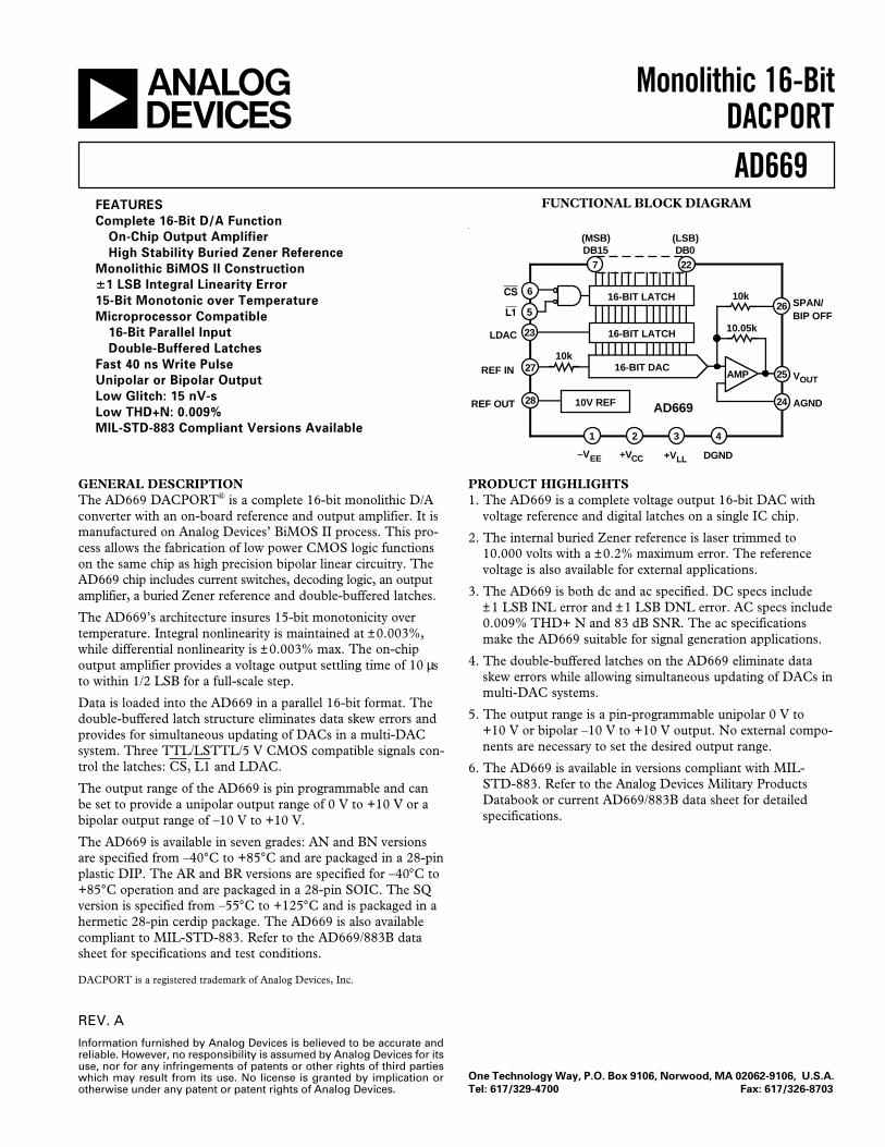
FUNCTIONAL BLOCK DIAGRAM
LDAC
SPAN/BIP OFF
AGND
DB15(MSB) (LSB)
DB0
DGND
CS
L1
REF IN
REF OUT
–VEE +VCC +VLL
VOUT
16-BIT LATCH
10k
AMP
AD669
227
6
5
23
27
28 10V REF
21 43
26
24
10k
10.05k16-BIT LATCH
16-BIT DAC25
REV. A
Information furnished by Analog Devices is believed to be accurate andreliable. However, no responsibility is assumed by Analog Devices for itsuse, nor for any infringements of patents or other rights of third partieswhich may result from its use. No license is granted by implication orotherwise under any patent or patent rights of Analog Devices.
a Monolithic 16-BitDACPORTAD669
FEATURES
Complete 16-Bit D/A Function
On-Chip Output Amplifier
High Stability Buried Zener Reference
Monolithic BiMOS II Construction
61 LSB Integral Linearity Error
15-Bit Monotonic over Temperature
Microprocessor Compatible
16-Bit Parallel Input
Double-Buffered Latches
Fast 40 ns Write Pulse
Unipolar or Bipolar Output
Low Glitch: 15 nV-s
Low THD+N: 0.009%
MIL-STD-883 Compliant Versions Available
GENERAL DESCRIPTIONThe AD669 DACPORT® is a complete 16-bit monolithic D/Aconverter with an on-board reference and output amplifier. It ismanufactured on Analog Devices’ BiMOS II process. This pro-cess allows the fabrication of low power CMOS logic functionson the same chip as high precision bipolar linear circuitry. TheAD669 chip includes current switches, decoding logic, an outputamplifier, a buried Zener reference and double-buffered latches.
The AD669’s architecture insures 15-bit monotonicity overtemperature. Integral nonlinearity is maintained at ±0.003%,while differential nonlinearity is ±0.003% max. The on-chipoutput amplifier provides a voltage output settling time of 10 µsto within 1/2 LSB for a full-scale step.
Data is loaded into the AD669 in a parallel 16-bit format. Thedouble-buffered latch structure eliminates data skew errors andprovides for simultaneous updating of DACs in a multi-DACsystem. Three TTL/LSTTL/5 V CMOS compatible signals con-trol the latches: CS, L1 and LDAC.
The output range of the AD669 is pin programmable and canbe set to provide a unipolar output range of 0 V to +10 V or abipolar output range of –10 V to +10 V.
The AD669 is available in seven grades: AN and BN versionsare specified from –40°C to +85°C and are packaged in a 28-pinplastic DIP. The AR and BR versions are specified for –40°C to+85°C operation and are packaged in a 28-pin SOIC. The SQversion is specified from –55°C to +125°C and is packaged in ahermetic 28-pin cerdip package. The AD669 is also availablecompliant to MIL-STD-883. Refer to the AD669/883B datasheet for specifications and test conditions.
DACPORT is a registered trademark of Analog Devices, Inc.
One Technology Way, P.O. Box 9106, Norwood, MA 02062-9106, U.S.A.
Tel: 617/329-4700 Fax: 617/326-8703
PRODUCT HIGHLIGHTS1. The AD669 is a complete voltage output 16-bit DAC with
voltage reference and digital latches on a single IC chip.
2. The internal buried Zener reference is laser trimmed to10.000 volts with a ±0.2% maximum error. The referencevoltage is also available for external applications.
3. The AD669 is both dc and ac specified. DC specs include±1 LSB INL error and ±1 LSB DNL error. AC specs include0.009% THD+ N and 83 dB SNR. The ac specificationsmake the AD669 suitable for signal generation applications.
4. The double-buffered latches on the AD669 eliminate dataskew errors while allowing simultaneous updating of DACs inmulti-DAC systems.
5. The output range is a pin-programmable unipolar 0 V to+10 V or bipolar –10 V to +10 V output. No external compo-nents are necessary to set the desired output range.
6. The AD669 is available in versions compliant with MIL-STD-883. Refer to the Analog Devices Military ProductsDatabook or current AD669/883B data sheet for detailedspecifications.
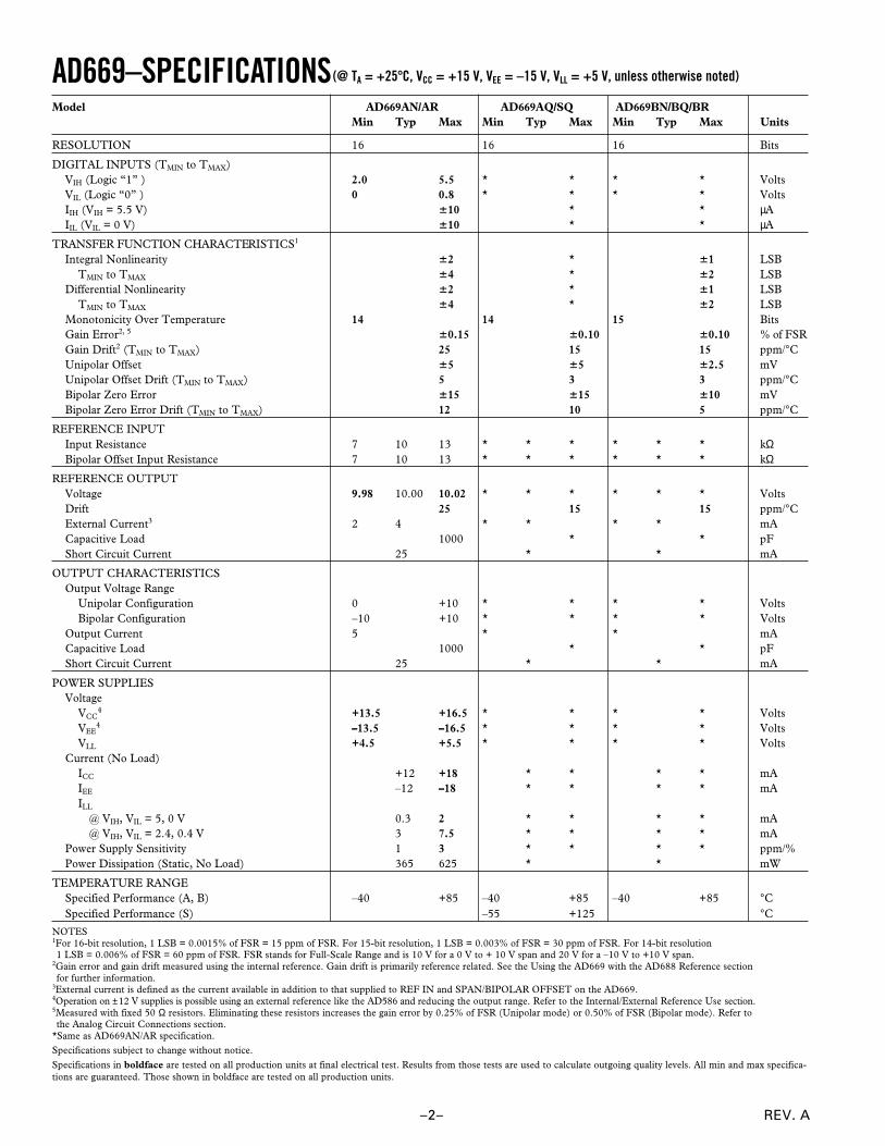
AD669–SPECIFICATIONSModel AD669AN/AR AD669AQ/SQ AD669BN/BQ/BR
Min Typ Max Min Typ Max Min Typ Max Units
RESOLUTION 16 16 16 Bits
DIGITAL INPUTS (TMIN to TMAX)VIH (Logic “1” ) 2.0 5.5 * * * * VoltsVIL (Logic “0” ) 0 0.8 * * * * VoltsIIH (VIH = 5.5 V) 610 * * µAIIL (VIL = 0 V) 610 * * µA
TRANSFER FUNCTION CHARACTERISTICS1
Integral Nonlinearity 62 * 61 LSBTMIN to TMAX 64 * 62 LSB
Differential Nonlinearity 62 * 61 LSBTMIN to TMAX 64 * 62 LSB
Monotonicity Over Temperature 14 14 15 BitsGain Error2, 5 60.15 60.10 60.10 % of FSRGain Drift2 (TMIN to TMAX) 25 15 15 ppm/°CUnipolar Offset 65 65 62.5 mVUnipolar Offset Drift (TMIN to TMAX) 5 3 3 ppm/°CBipolar Zero Error 615 615 610 mVBipolar Zero Error Drift (TMIN to TMAX) 12 10 5 ppm/°C
REFERENCE INPUTInput Resistance 7 10 13 * * * * * * kΩBipolar Offset Input Resistance 7 10 13 * * * * * * kΩ
REFERENCE OUTPUTVoltage 9.98 10.00 10.02 * * * * * * VoltsDrift 25 15 15 ppm/°CExternal Current3 2 4 * * * * mACapacitive Load 1000 * * pFShort Circuit Current 25 * * mA
OUTPUT CHARACTERISTICSOutput Voltage Range
Unipolar Configuration 0 +10 * * * * VoltsBipolar Configuration –10 +10 * * * * Volts
Output Current 5 * * mACapacitive Load 1000 * * pFShort Circuit Current 25 * * mA
POWER SUPPLIESVoltage
VCC4 +13.5 +16.5 * * * * Volts
VEE4 –13.5 –16.5 * * * * Volts
VLL +4.5 +5.5 * * * * VoltsCurrent (No Load)
ICC +12 +18 * * * * mAIEE –12 –18 * * * * mAILL
@ VIH, VIL = 5, 0 V 0.3 2 * * * * mA@ VIH, VIL = 2.4, 0.4 V 3 7.5 * * * * mA
Power Supply Sensitivity 1 3 * * * * ppm/%Power Dissipation (Static, No Load) 365 625 * * mW
TEMPERATURE RANGESpecified Performance (A, B) –40 +85 –40 +85 –40 +85 °CSpecified Performance (S) –55 +125 °C
NOTES1For 16-bit resolution, 1 LSB = 0.0015% of FSR = 15 ppm of FSR. For 15-bit resolution, 1 LSB = 0.003% of FSR = 30 ppm of FSR. For 14-bit resolution1 LSB = 0.006% of FSR = 60 ppm of FSR. FSR stands for Full-Scale Range and is 10 V for a 0 V to + 10 V span and 20 V for a –10 V to +10 V span.
2Gain error and gain drift measured using the internal reference. Gain drift is primarily reference related. See the Using the AD669 with the AD688 Reference sectionfor further information.
3External current is defined as the current available in addition to that supplied to REF IN and SPAN/BIPOLAR OFFSET on the AD669.4Operation on ±12 V supplies is possible using an external reference like the AD586 and reducing the output range. Refer to the Internal/External Reference Use section.5Measured with fixed 50 Ω resistors. Eliminating these resistors increases the gain error by 0.25% of FSR (Unipolar mode) or 0.50% of FSR (Bipolar mode). Refer tothe Analog Circuit Connections section.
*Same as AD669AN/AR specification.
Specifications subject to change without notice.
Specifications in boldface are tested on all production units at final electrical test. Results from those tests are used to calculate outgoing quality levels. All min and max specifica-tions are guaranteed. Those shown in boldface are tested on all production units.
(@ TA = +258C, VCC = +15 V, VEE = –15 V, VLL = +5 V, unless otherwise noted)
REV. A–2–
AD669
REV. A –3–
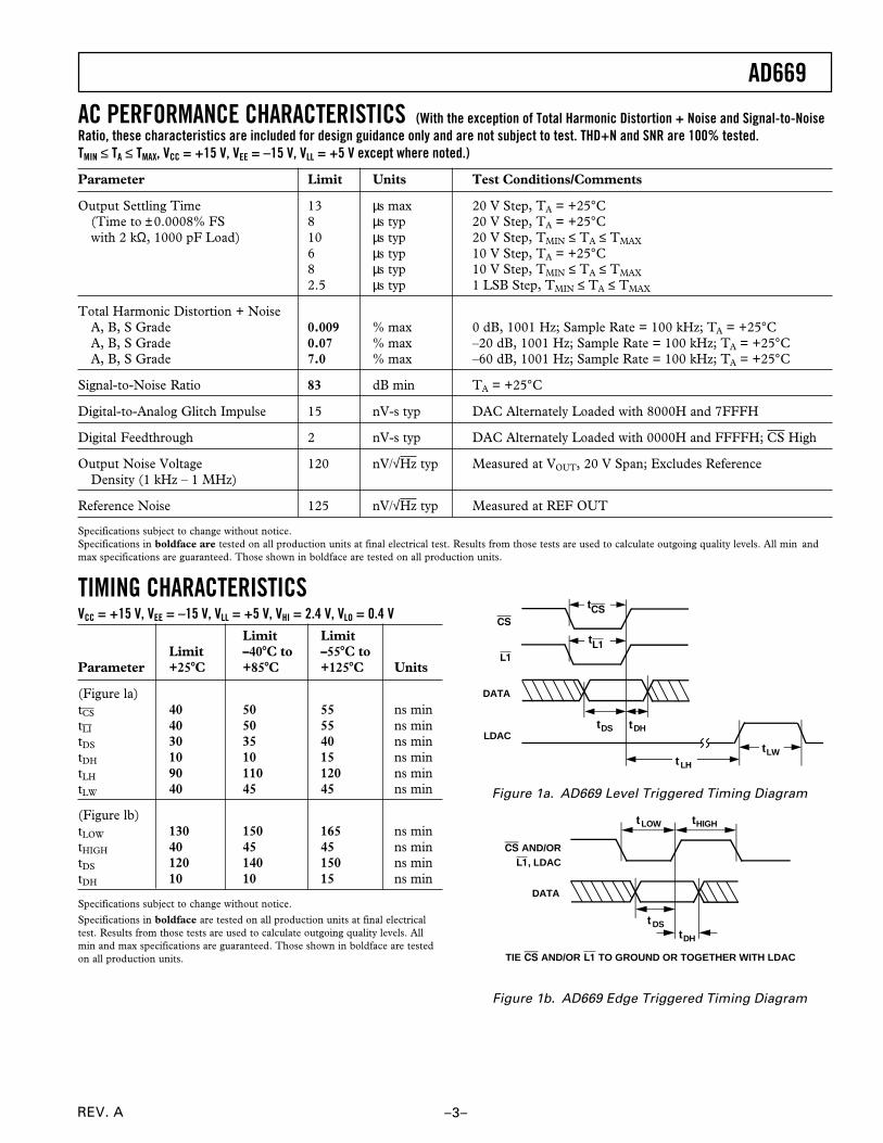
TIMING CHARACTERISTICSVCC = +15 V, VEE = –15 V, VLL = +5 V, VHI = 2.4 V, VLO = 0.4 V
Limit LimitLimit –408C to –558C to
Parameter +258C +858C +1258C Units
(Figure la)tCS 40 50 55 ns mintLI 40 50 55 ns mintDS 30 35 40 ns mintDH 10 10 15 ns mintLH 90 110 120 ns mintLW 40 45 45 ns min
(Figure lb)tLOW 130 150 165 ns mintHIGH 40 45 45 ns mintDS 120 140 150 ns mintDH 10 10 15 ns min
Specifications subject to change without notice.
Specifications in boldface are tested on all production units at final electricaltest. Results from those tests are used to calculate outgoing quality levels. Allmin and max specifications are guaranteed. Those shown in boldface are testedon all production units.
AC PERFORMANCE CHARACTERISTICS
Parameter Limit Units Test Conditions/Comments
Output Settling Time 13 µs max 20 V Step, TA = +25°C(Time to ±0.0008% FS 8 µs typ 20 V Step, TA = +25°Cwith 2 kΩ, 1000 pF Load) 10 µs typ 20 V Step, TMIN ≤ TA ≤ TMAX
6 µs typ 10 V Step, TA = +25°C8 µs typ 10 V Step, TMIN ≤ TA ≤ TMAX
2.5 µs typ 1 LSB Step, TMIN ≤ TA ≤ TMAX
Total Harmonic Distortion + NoiseA, B, S Grade 0.009 % max 0 dB, 1001 Hz; Sample Rate = 100 kHz; TA = +25°CA, B, S Grade 0.07 % max –20 dB, 1001 Hz; Sample Rate = 100 kHz; TA = +25°CA, B, S Grade 7.0 % max –60 dB, 1001 Hz; Sample Rate = 100 kHz; TA = +25°C
Signal-to-Noise Ratio 83 dB min TA = +25°C
Digital-to-Analog Glitch Impulse 15 nV-s typ DAC Alternately Loaded with 8000H and 7FFFH
Digital Feedthrough 2 nV-s typ DAC Alternately Loaded with 0000H and FFFFH; CS High
Output Noise Voltage 120 nV/√Hz typ Measured at VOUT, 20 V Span; Excludes ReferenceDensity (1 kHz – 1 MHz)
Reference Noise 125 nV/√Hz typ Measured at REF OUT
Specifications subject to change without notice.Specifications in boldface are tested on all production units at final electrical test. Results from those tests are used to calculate outgoing quality levels. All min andmax specifications are guaranteed. Those shown in boldface are tested on all production units.
(With the exception of Total Harmonic Distortion + Noise and Signal-to-NoiseRatio, these characteristics are included for design guidance only and are not subject to test. THD+N and SNR are 100% tested.TMIN ≤ TA ≤ TMAX, VCC = +15 V, VEE = –15 V, VLL = +5 V except where noted.)
DATA
LDACtDS tDH
CS
tLWtLH
L1
tCS
tL1
Figure 1a. AD669 Level Triggered Timing Diagram
DATA
tDStDH
CS AND/OR L1, LDAC
TIE CS AND/OR L1 TO GROUND OR TOGETHER WITH LDAC
tLOW tHIGH
Figure 1b. AD669 Edge Triggered Timing Diagram

AD669
REV. A–4–
ORDERING GUIDE
Linearity GainTemperature Error Max TC max Package Package
Model Range TMIN–TMAX ppm/8C Description Option*
AD669AN –40°C to +85°C ±4 LSB 25 Plastic DIP N-28AD669AR –40°C to +85°C ±4 LSB 25 SOIC R-28AD669BN –40°C to +85°C ±2 LSB 15 Plastic DIP N-28AD669BR –40°C to +85°C ±2 LSB 15 SOIC R-28AD669AQ –40°C to +85°C ±4 LSB 15 Cerdip Q-28AD669BQ –40°C to +85°C ±2 LSB 15 Cerdip Q-28AD669SQ –55°C to +125°C ±4 LSB 15 Cerdip Q-28AD669/883B** –55°C to +125°C ** ** ** **
** N = Plastic DIP; Q = Cerdip; R = SOIC.** Refer to AD669/883B military data sheet.
ESD SENSITIVITYThe AD669 features input protection circuitry consisting of large transistors and polysilicon seriesresistors to dissipate both high-energy discharges (Human Body Model) and fast, low-energy pulses(Charged Device Model). Per Method 3015.2 of MIL-STD-883: C, the AD669 has been classifiedas a Class 2 device.
Proper ESD precautions are strongly recommended to avoid functional damage or performancedegradation. Charges as high as 4000 volts readily accumulate on the human body and testequipment and discharge without detection. Unused devices must be stored in conductive foam orshunts, and the foam should be discharged to the destination socket before devices are removed.For further information on ESD precautions, refer to Analog Devices’ ESD Prevention Manual.
WARNING!
ESD SENSITIVE DEVICE
ABSOLUTE MAXIMUM RATINGS*
VCC to AGND . . . . . . . . . . . . . . . . . . . . . . . –0.3 V to +17.0 VVEE to AGND . . . . . . . . . . . . . . . . . . . . . . . +0.3 V to –17.0 VVLL to DGND . . . . . . . . . . . . . . . . . . . . . . . . . . –0.3 V to +7 VAGND to DGND . . . . . . . . . . . . . . . . . . . . . . . . . . . . . . ±1 VDigital Inputs (Pins 5 through 23) to DGND . . . . . . –1.0 V to . . . . . . . . . . . . . . . . . . . . . . . . . . . . . . . . . . . . . . . . . . . . +7.0 VREF IN to AGND . . . . . . . . . . . . . . . . . . . . . . . . . . . . ±10.5 VSpan/Bipolar Offset to AGND . . . . . . . . . . . . . . . . . . . ±10.5 VREF OUT, VOUT . . . . . . Indefinite Short To AGND, DGND, . . . . . . . . . . . . . . . . . . . . . . . . . . . . . . . . . . . VCC, VEE, and VLL
Power Dissipation (Any Package)To +60°C . . . . . . . . . . . . . . . . . . . . . . . . . . . . . . . . 1000 mWDerates above +60°C . . . . . . . . . . . . . . . . . . . . . .8.7 mW/°C
Storage Temperature . . . . . . . . . . . . . . . . . . . –65°C to +150°CLead Temperature (Soldering, 10 sec) . . . . . . . . . . . . . +300°C*Stresses above those listed under “Absolute Maximum Ratings” may cause
permanent damage to the device. This is a stress rating only, and functionaloperation of the device at these or any other conditions above those indicated inthe operational section of this specification is not implied. Exposure to absolutemaximum rating conditions for extended periods may affect device reliability.
PIN CONFIGURATION
DB15
DB14
DB13
DB12
DB11
DB10
DB9
DB8
DGND
VEE
VCC
VLL
CS
L1
1
2
3
4
5
6
7
8
9
10
11
12
13
14
28
27
26
25
24
23
22
21
20
19
18
17
16
15
TOP VIEW(Not to Scale)
DB7
DB6
DB5
DB4
DB3
DB2
AGND
LDAC
DB0
DB1
AD669
REF OUT
REF IN
VOUT
SPAN/BIPOFFSET
TH
D +
N –
%
TEMPERATURE – °C
10
0.001125
0.01
–25–50
0.1
1
1007550250
–60dB
–20dB
0dB
THD+N vs. Temperature
FREQUENCY – Hz
TH
D +
N –
%
10
0.001
0.01
0.1
1
100 100001000
–60dB
–20dB
0dB
THD+N vs. Frequency
AD669
REV. A –5–
DEFINITIONS OF SPECIFICATIONSINTEGRAL NONLINEARITY: Analog Devices defines inte-gral nonlinearity as the maximum deviation of the actual, ad-justed DAC output from the ideal analog output (a straight linedrawn from 0 to FS–1 LSB) for any bit combination. This isalso referred to as relative accuracy.
DIFFERENTIAL NONLINEARITY: Differential nonlinearityis the measure of the change in the analog output, normalized tofull scale, associated with a 1 LSB change in the digital inputcode. Monotonic behavior requires that the differential linearityerror be within ±1 LSB over the temperature range of interest.
MONOTONICITY: A DAC is monotonic if the output eitherincreases or remains constant for increasing digital inputs withthe result that the output will always be a single-valued functionof the input.
GAIN ERROR: Gain error is a measure of the output error be-tween an ideal DAC and the actual device output with all 1sloaded after offset error has been adjusted out.
OFFSET ERROR: Offset error is a combination of the offseterrors of the voltage-mode DAC and the output amplifier and ismeasured with all 0s loaded in the DAC.
BIPOLAR ZERO ERROR: When the AD669 is connected forbipolar output and 10 . . . 000 is loaded in the DAC, the devia-tion of the analog output from the ideal midscale value of 0 V iscalled the bipolar zero error.
DRIFT: Drift is the change in a parameter (such as gain, offsetand bipolar zero) over a specified temperature range. The drifttemperature coefficient, specified in ppm/°C, is calculated bymeasuring the parameter at TMIN, 25°C and TMAX and dividingthe change in the parameter by the corresponding temperaturechange.
TOTAL HARMONIC DISTORTION + NOISE: Total har-monic distortion + noise (THD+N) is defined as the ratio of thesquare root of the sum of the squares of the values of the har-monics and noise to the value of the fundamental input fre-quency. It is usually expressed in percent (%).
THD+N is a measure of the magnitude and distribution of lin-earity error, differential linearity error, quantization error andnoise. The distribution of these errors may be different, depend-ing upon the amplitude of the output signal. Therefore, to bethe most useful, THD+N should be specified for both large andsmall signal amplitudes.
SIGNAL-TO-NOISE RATIO: The signal-to-noise ratio is de-fined as the ratio of the amplitude of the output when a full-scale signal is present to the output with no signal present. Thisis measured in dB.
DIGITAL-TO-ANALOG GLITCH IMPULSE: This is theamount of charge injected from the digital inputs to the analogoutput when the inputs change state. This is measured at halfscale when the DAC switches around the MSB and as manyas possible switches change state, i.e., from 011 . . . 111 to100 . . . 000.
DIGITAL FEEDTHROUGH: When the DAC is not selected(i.e., CS is held high), high frequency logic activity on the digi-tal inputs is capacitively coupled through the device to show upas noise on the VOUT pin. This noise is digital feedthrough.
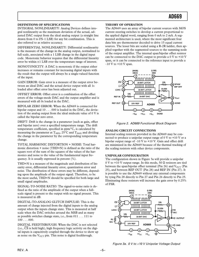
THEORY OF OPERATIONThe AD669 uses an array of bipolar current sources with MOScurrent steering switches to develop a current proportional tothe applied digital word, ranging from 0 mA to 2 mA. A seg-mented architecture is used, where the most significant fourdata bits are thermometer decoded to drive 15 equal currentsources. The lesser bits are scaled using a R-2R ladder, then ap-plied together with the segmented sources to the summing nodeof the output amplifier. The internal span/bipolar offset resistorcan be connected to the DAC output to provide a 0 V to +10 Vspan, or it can be connected to the reference input to provide a–10 V to +10 V span.
SPAN/BIP OFF
AGND
DGND
REF IN
REF OUT
VOUT
LDAC
DB15(MSB) (LSB)
DB0
CS
L1
–VEE +VCC +VLL
16-BIT LATCH
10k
AMP
AD669
227
6
5
23
27
28 10V REF
21 43
26
24
10k
10.05k16-BIT LATCH
16-BIT DAC25
Figure 2. AD669 Functional Block Diagram
ANALOG CIRCUIT CONNECTIONSInternal scaling resistors provided in the AD669 may be con-nected to produce a unipolar output range of 0 V to +10 V or abipolar output range of –10 V to +10 V. Gain and offset driftare minimized in the AD669 because of the thermal tracking ofthe scaling resistors with other device components.
UNIPOLAR CONFIGURATIONThe configuration shown in Figure 3a will provide a unipolar0 V to +10 V output range. In this mode, 50 Ω resistors are tiedbetween the span/bipolar offset terminal (Pin 26) and VOUT (Pin25), and between REF OUT (Pin 28) and REF IN (Pin 27). Itis possible to use the AD669 without any external componentsby tying Pin 28 directly to Pin 27 and Pin 26 directly to Pin 25.Eliminating these resistors will increase the gain error by 0.25%of FSR.
OUTPUT
GND
LDAC
DB15(MSB) (LSB)
DB0
CS
L1
–VEE +VCC +VLL
16-BIT LATCH
10k
AMP
AD669
227
6
5
23
27
28 10V REF
21 43
10k
10.05k16-BIT LATCH
16-BIT DAC
26
25
24
R150Ω
R250Ω
Figure 3a. 0 V to +10 V Unipolar Voltage Output
AD669
REV. A–6–
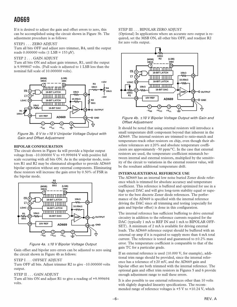
If it is desired to adjust the gain and offset errors to zero, thiscan be accomplished using the circuit shown in Figure 3b. Theadjustment procedure is as follows:
STEP1 . . . ZERO ADJUSTTurn all bits OFF and adjust zero trimmer, R4, until the outputreads 0.000000 volts (1 LSB = 153 µV).
STEP 2 . . . GAIN ADJUSTTurn all bits ON and adjust gain trimmer, R1, until the outputis 9.999847 volts. (Full scale is adjusted to 1 LSB less than thenominal full scale of 10.000000 volts).
OUTPUT
GND
LDAC
DB15(MSB) (LSB)
DB0
CS
L1
16-BIT LATCH
10kV
AMP
AD669
227
6
5
23
27
28 10V REF
21 43
10kV
10.05kV16-BIT LATCH
16-BIT DAC
26
25
24
R250V
R316kV R4
10kV
+15V
–15V
R1100V
–VEE +VCC +VLL
Figure 3b. 0 V to +10 V Unipolar Voltage Output with
Gain and Offset Adjustment
BIPOLAR CONFIGURATIONThe circuit shown in Figure 4a will provide a bipolar outputvoltage from –10.000000 V to +9.999694 V with positive fullscale occurring with all bits ON. As in the unipolar mode, resis-tors R1 and R2 may be eliminated altogether to provide AD669bipolar operation without any external components. Eliminatingthese resistors will increase the gain error by 0.50% of FSR inthe bipolar mode.
R1
50VOUTPUT
GND
LDAC
DB15(MSB) (LSB)
DB0
CS
L116-BIT LATCH
10kV
AMP
AD669
227
6
5
23
27
10V REF
21 43
26
24
10kV
10.05kV16-BIT LATCH
16-BIT DAC25
28
R2
50V
–VEE +VCC +VLL
Figure 4a. ±10 V Bipolar Voltage Output
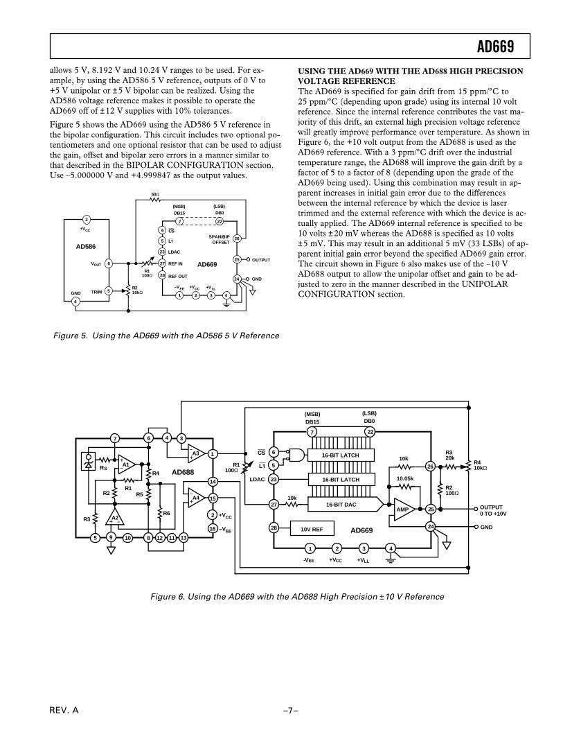
Gain offset and bipolar zero errors can be adjusted to zero usingthe circuit shown in Figure 4b as follows:
STEP I . . . OFFSET ADJUSTTurn OFF all bits. Adjust trimmer R2 to give –10.000000 voltsoutput.
STEP II . . . GAIN ADJUSTTurn all bits ON and adjust R1 to give a reading of +9.999694volts.
STEP III . . . BIPOLAR ZERO ADJUST(Optional) In applications where an accurate zero output is re-quired, set the MSB ON, all other bits OFF, and readjust R2for zero volts output.
100VR1
OUTPUT
GND
LDAC
DB15(MSB) (LSB)
DB0
CS
L1
16-BIT LATCH
10kV
AMP
AD669
227
6
5
23
27
10V REF
21 43
26
24
10kV
10.05kV16-BIT LATCH
16-BIT DAC25
28
100VR2
–VEE +VCC +VLL
Figure 4b. ±10 V Bipolar Voltage Output with Gain and
Offset Adjustment
It should be noted that using external resistors will introduce asmall temperature drift component beyond that inherent in theAD669. The internal resistors are trimmed to ratio-match andtemperature-track other resistors on chip, even though their ab-solute tolerances are ±20% and absolute temperature coeffi-cients are approximately –50 ppm/°C. In the case that externalresistors are used, the temperature coefficient mismatch be-tween internal and external resistors, multiplied by the sensitiv-ity of the circuit to variations in the external resistor value, willbe the resultant additional temperature drift.
INTERNAL/EXTERNAL REFERENCE USEThe AD669 has an internal low noise buried Zener diode refer-ence which is trimmed for absolute accuracy and temperaturecoefficient. This reference is buffered and optimized for use in ahigh speed DAC and will give long-term stability equal or supe-rior to the best discrete Zener diode references. The perfor-mance of the AD669 is specified with the internal referencedriving the DAC since all trimming and testing (especially forgain and bipolar offset) is done in this configuration.
The internal reference has sufficient buffering to drive externalcircuitry in addition to the reference currents required for theDAC (typically 1 mA to REF IN and 1 mA to BIPOLAR OFF-SET). A minimum of 2 mA is available for driving externalloads. The AD669 reference output should be buffered with anexternal op amp if it is required to supply more than 4 mA totalcurrent. The reference is tested and guaranteed to ±0.2% maxerror. The temperature coefficient is comparable to that of thegain TC for a particular grade.
If an external reference is used (10.000 V, for example), addi-tional trim range should be provided, since the internal refer-ence has a tolerance of ±20 mV, and the AD669 gain andbipolar offset are both trimmed with the internal reference. Theoptional gain and offset trim resistors in Figures 5 and 6 provideenough adjustment range to null these errors.
It is also possible to use external references other than 10 voltswith slightly degraded linearity specifications. The recom-mended range of reference voltages is +5 V to +10.24 V, which
AD669
REV. A –7–
allows 5 V, 8.192 V and 10.24 V ranges to be used. For ex-ample, by using the AD586 5 V reference, outputs of 0 V to+5 V unipolar or ±5 V bipolar can be realized. Using theAD586 voltage reference makes it possible to operate theAD669 off of ±12 V supplies with 10% tolerances.
Figure 5 shows the AD669 using the AD586 5 V reference inthe bipolar configuration. This circuit includes two optional po-tentiometers and one optional resistor that can be used to adjustthe gain, offset and bipolar zero errors in a manner similar tothat described in the BIPOLAR CONFIGURATION section.Use –5.000000 V and +4.999847 as the output values.
50Ω
OUTPUT
GND
LDAC
DB15
(MSB) (LSB)
DB0
CS
L1
–VEE +VCC +VLL
AD669
227
6
5
23
27
21 43
26
25
R1100Ω
R210kΩ
4
6
5
AD586
+VCC
28
REF IN
REF OUT
VOUT
TRIMGND
SPAN/BIPOFFSET
24
2
Figure 5. Using the AD669 with the AD586 5 V Reference
USING THE AD669 WITH THE AD688 HIGH PRECISIONVOLTAGE REFERENCEThe AD669 is specified for gain drift from 15 ppm/°C to25 ppm/°C (depending upon grade) using its internal 10 voltreference. Since the internal reference contributes the vast ma-jority of this drift, an external high precision voltage referencewill greatly improve performance over temperature. As shown inFigure 6, the +10 volt output from the AD688 is used as theAD669 reference. With a 3 ppm/°C drift over the industrialtemperature range, the AD688 will improve the gain drift by afactor of 5 to a factor of 8 (depending upon the grade of theAD669 being used). Using this combination may result in ap-parent increases in initial gain error due to the differencesbetween the internal reference by which the device is lasertrimmed and the external reference with which the device is ac-tually applied. The AD669 internal reference is specified to be10 volts ±20 mV whereas the AD688 is specified as 10 volts±5 mV. This may result in an additional 5 mV (33 LSBs) of ap-parent initial gain error beyond the specified AD669 gain error.The circuit shown in Figure 6 also makes use of the –10 VAD688 output to allow the unipolar offset and gain to be ad-justed to zero in the manner described in the UNIPOLARCONFIGURATION section.
R2100Ω
R320k
R1100Ω
LDAC
DB15(MSB) (LSB)
DB0
CS
L1
-VEE +VCC +VLL
16-BIT LATCH
10k
AMP
AD669
227
6
5
23
27
28 10V REF
21 43
26
24
10k
10.05k16-BIT LATCH
16-BIT DAC25
R410kΩ
7 6 3
1
14
15
2
16
5 10 8 12 11 13
R1R2 R5
R6R3
AD688
A3
A1
A4
A2
R4RS
9
4
GND
OUTPUT0 TO +10V+VCC
–VEE
Figure 6. Using the AD669 with the AD688 High Precision ±10 V Reference
AD669
REV. A–8–
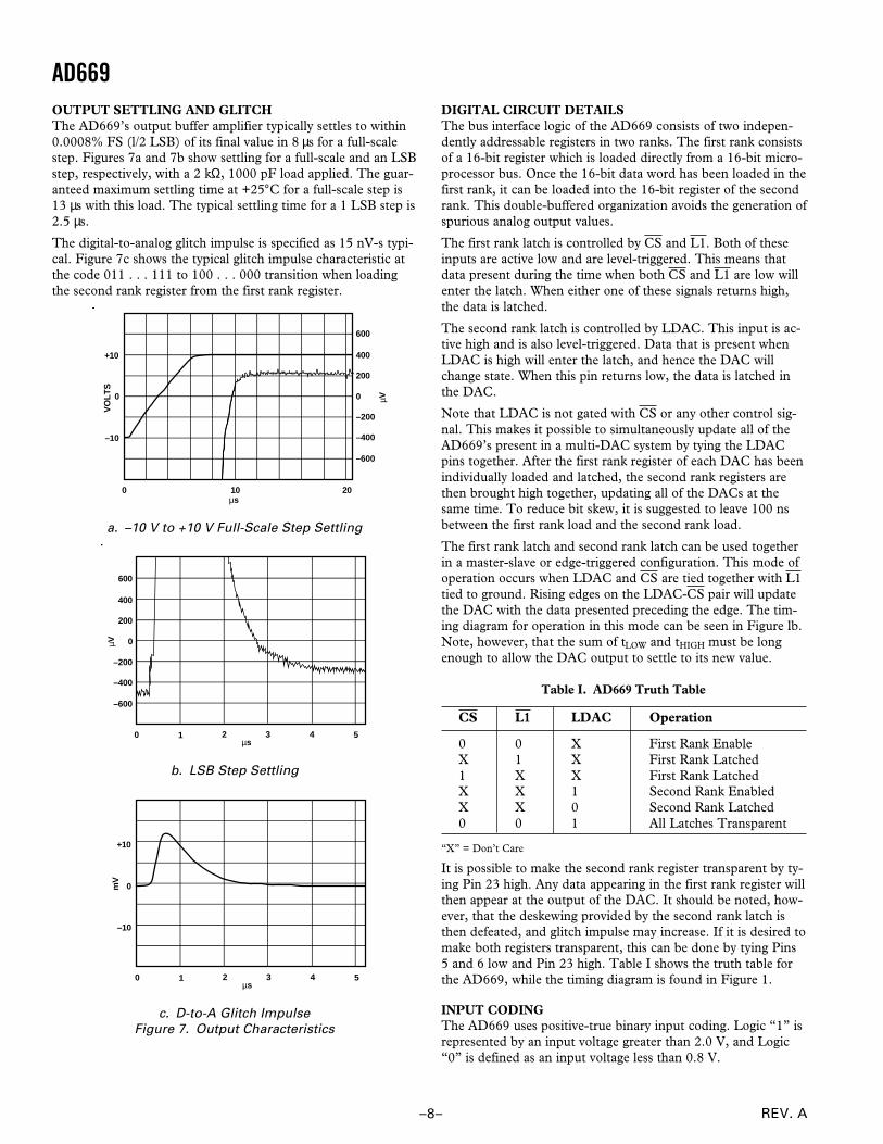
OUTPUT SETTLING AND GLITCHThe AD669’s output buffer amplifier typically settles to within0.0008% FS (l/2 LSB) of its final value in 8 µs for a full-scalestep. Figures 7a and 7b show settling for a full-scale and an LSBstep, respectively, with a 2 kΩ, 1000 pF load applied. The guar-anteed maximum settling time at +25°C for a full-scale step is13 µs with this load. The typical settling time for a 1 LSB step is2.5 µs.
The digital-to-analog glitch impulse is specified as 15 nV-s typi-cal. Figure 7c shows the typical glitch impulse characteristic atthe code 011 . . . 111 to 100 . . . 000 transition when loadingthe second rank register from the first rank register.
20
–10
0
0
+10
10
600
400
200
0
–200
–400
–600
VO
LT
S
µs
µV
a. –10 V to +10 V Full-Scale Step Settling
50
0
600
400
200
–200
–400
–600
µs
µV
1 2 3 4
b. LSB Step Settling
50
0
+10
–10
µs
mV
1 2 3 4
c. D-to-A Glitch Impulse
Figure 7. Output Characteristics
DIGITAL CIRCUIT DETAILSThe bus interface logic of the AD669 consists of two indepen-dently addressable registers in two ranks. The first rank consistsof a 16-bit register which is loaded directly from a 16-bit micro-processor bus. Once the 16-bit data word has been loaded in thefirst rank, it can be loaded into the 16-bit register of the secondrank. This double-buffered organization avoids the generation ofspurious analog output values.
The first rank latch is controlled by CS and L1. Both of theseinputs are active low and are level-triggered. This means thatdata present during the time when both CS and L1 are low willenter the latch. When either one of these signals returns high,the data is latched.
The second rank latch is controlled by LDAC. This input is ac-tive high and is also level-triggered. Data that is present whenLDAC is high will enter the latch, and hence the DAC willchange state. When this pin returns low, the data is latched inthe DAC.
Note that LDAC is not gated with CS or any other control sig-nal. This makes it possible to simultaneously update all of theAD669’s present in a multi-DAC system by tying the LDACpins together. After the first rank register of each DAC has beenindividually loaded and latched, the second rank registers arethen brought high together, updating all of the DACs at thesame time. To reduce bit skew, it is suggested to leave 100 nsbetween the first rank load and the second rank load.
The first rank latch and second rank latch can be used togetherin a master-slave or edge-triggered configuration. This mode ofoperation occurs when LDAC and CS are tied together with L1tied to ground. Rising edges on the LDAC-CS pair will updatethe DAC with the data presented preceding the edge. The tim-ing diagram for operation in this mode can be seen in Figure lb.Note, however, that the sum of tLOW and tHIGH must be longenough to allow the DAC output to settle to its new value.
Table I. AD669 Truth Table
CS L1 LDAC Operation
0 0 X First Rank EnableX 1 X First Rank Latched1 X X First Rank LatchedX X 1 Second Rank EnabledX X 0 Second Rank Latched0 0 1 All Latches Transparent
“X” = Don’t Care
It is possible to make the second rank register transparent by ty-ing Pin 23 high. Any data appearing in the first rank register willthen appear at the output of the DAC. It should be noted, how-ever, that the deskewing provided by the second rank latch isthen defeated, and glitch impulse may increase. If it is desired tomake both registers transparent, this can be done by tying Pins5 and 6 low and Pin 23 high. Table I shows the truth table forthe AD669, while the timing diagram is found in Figure 1.
INPUT CODINGThe AD669 uses positive-true binary input coding. Logic “1” isrepresented by an input voltage greater than 2.0 V, and Logic“0” is defined as an input voltage less than 0.8 V.
AD669
REV. A –9–
Unipolar coding is straight binary, where all zeros (0000H) onthe data inputs yields a zero analog output and all ones(FFFFH) yields an analog output 1 LSB below full scale.
Bipolar coding is offset binary, where an input code of 0000Hyields a minus full-scale output, an input of FFFFH yields anoutput 1 LSB below positive full scale, and zero occurs for aninput code with only the MSB on (8000H).
The AD669 can be used with twos complement input coding ifan inverter is used on the MSB (DB15).
DIGITAL INPUT CONSIDERATIONSThe threshold of the digital input circuitry is set at 1.4 volts.The input lines can thus interface with any type of 5 volt logic.
The AD669 data and control inputs will float to indeterminatelogic states if left open. It is important that CS and L1 be con-nected to DGND and Chat LDAC be tied to VLL if these pinsare not used.
Fanout for the AD669 is 40 when used with a standard lowpower Schottky gate output device.
16-BIT MICROPROCESSOR INTERFACEThe 16-bit parallel registers of the AD669 allow direct interfac-ing to 16-bit general purpose and DSP microprocessor buses.The following examples illustrate typical AD669 interfaceconfigurations.
AD669 TO ADSP-2101 INTERFACEThe flexible interface of the AD669 minimizes the required“glue” logic when it is connected in configurations such as theone shown in Figure 8. The AD669 is mapped into the ADSP-2101’s memory space and requires two wait states using a 12.5MHz processor clock.
In this configuration, the ADSP-2101 is set up to use the inter-nal timer to interrupt the processor at the desired sample rate.The WR pin and data lines D8–D23 from the ADSP-2101 aretied directly to the L1 and DB0 through DB15 pins of theAD669, respectively. The decoded signal CS1 is connected toboth CS and LDAC. When a timer interrupt is detected, theADSP-2101 automatically vectors to the appropriate serviceroutine with minimal overhead. The interrupt routine then in-structs the processor to execute a data memory write to the ad-dress of the AD669.
The WR pin and CS1 both go low causing the first 16-bit latchinside the AD669 to be transparent. The data present in the firstrank is then latched by the rising edge of WR. The rising edgeof CS1 will cause the second rank 16-bit latch to becometransparent updating the output of the DAC. The length ofWR is extended by two wait states to comply with the timingrequirements of tLOW shown in Figure 1b. It is important tolatch the data with the rising edge of WR rather than the decodedCS1. This is necessary to comply with the tDH specification ofthe AD669.
A0
D8
ADSP-2101
DGND
+5V
DECODER
ADDRESS BUS
LDAC
AD669
DGNDDB0
DATA BUS
DMS
WR
CS1
CS
L1
A13
DB15
D23
VLL
VLL
VOUT
a. ADSP-2101 to AD669 Interface
A13
A12
A11
DMS
CS1
b. Typical Address Decoder
Figure 8. ADSP-2101 to AD669 Interface
Figure 8b shows the circuitry a typical decoder might include.In this case, a data memory write to any address in the range3000H to 3400H will result in the AD669 being updated. Thesedecoders will vary greatly depending on the number of devicesmemory-mapped by the processor.
AD669 TO DSP56001 INTERFACEFigure 9 shows the interface between the AD669 and theDSP56001. Like the ADSP-2101, the AD669 is mapped intothe DSP56001’s memory space. This application was testedwith a processor clock of 20.48 MHz (tCYC = 97.66 ns) althoughfaster rates are possible.
An external clock connected to the IRQA pin of the DSP56001interrupts the processor at the desired sample rate. If ac perfor-mance is important, this clock should be synchronous with theDSP56001 processor clock. Asynchronous clocks will cause jit-ter on the latch signal due to the uncertainty associated with theacknowledgment of the interrupt. A synchronous clock is easilygenerated by dividing down the clock from the DSP crystal. Ifac performance is not important, it is not necessary for IRQA tobe synchronous.
After the interrupt is acknowledged, the interrupt routine ini-tiates a memory write cycle. All of the AD669 control inputs are
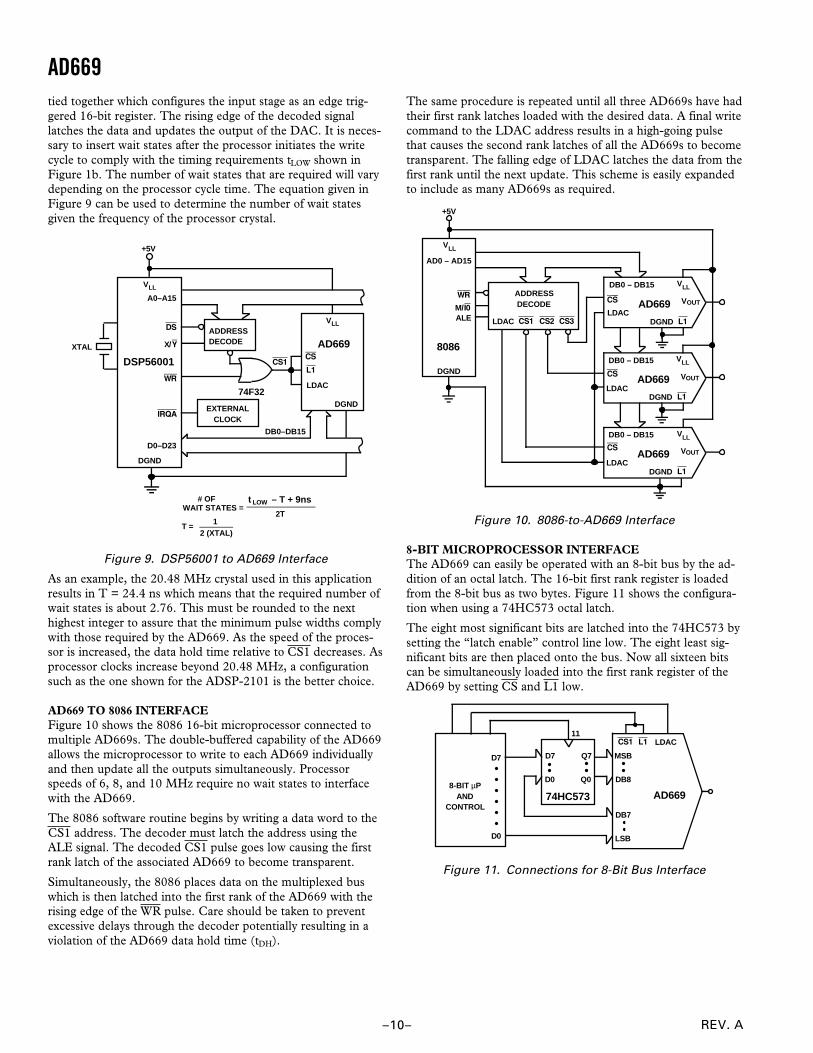
AD669
REV. A–10–
tied together which configures the input stage as an edge trig-gered 16-bit register. The rising edge of the decoded signallatches the data and updates the output of the DAC. It is neces-sary to insert wait states after the processor initiates the writecycle to comply with the timing requirements tLOW shown inFigure 1b. The number of wait states that are required will varydepending on the processor cycle time. The equation given inFigure 9 can be used to determine the number of wait statesgiven the frequency of the processor crystal.
A0–A15
DSP56001
D0–D23
DGND
+5V
EXTERNALCLOCK
ADDRESSDECODE
74F32LDAC
AD669
DGND
DB0–DB15
XTALCS
L1
DS
X/Y
WR
IRQA
VLL
CS1
T = 1
2 (XTAL)
t – T + 9ns
2T
LOW# OF WAIT STATES =
VLL
Figure 9. DSP56001 to AD669 Interface
As an example, the 20.48 MHz crystal used in this applicationresults in T = 24.4 ns which means that the required number ofwait states is about 2.76. This must be rounded to the nexthighest integer to assure that the minimum pulse widths complywith those required by the AD669. As the speed of the proces-sor is increased, the data hold time relative to CS1 decreases. Asprocessor clocks increase beyond 20.48 MHz, a configurationsuch as the one shown for the ADSP-2101 is the better choice.
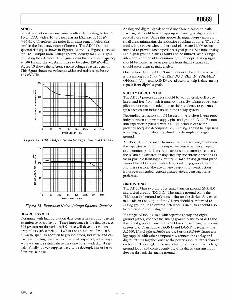
AD669 TO 8086 INTERFACEFigure 10 shows the 8086 16-bit microprocessor connected tomultiple AD669s. The double-buffered capability of the AD669allows the microprocessor to write to each AD669 individuallyand then update all the outputs simultaneously. Processorspeeds of 6, 8, and 10 MHz require no wait states to interfacewith the AD669.
The 8086 software routine begins by writing a data word to theCS1 address. The decoder must latch the address using theALE signal. The decoded CS1 pulse goes low causing the firstrank latch of the associated AD669 to become transparent.
Simultaneously, the 8086 places data on the multiplexed buswhich is then latched into the first rank of the AD669 with therising edge of the WR pulse. Care should be taken to preventexcessive delays through the decoder potentially resulting in aviolation of the AD669 data hold time (tDH).
The same procedure is repeated until all three AD669s have hadtheir first rank latches loaded with the desired data. A final writecommand to the LDAC address results in a high-going pulsethat causes the second rank latches of all the AD669s to becometransparent. The falling edge of LDAC latches the data from thefirst rank until the next update. This scheme is easily expandedto include as many AD669s as required.
8086
DGND
+5V
ALE
WR
M/I0
ADDRESSDECODE
LDAC CS1 CS2 CS3
DGND L1
DB0 – DB15
LDACAD669 VOUT
AD0 – AD15
DGND L1
DB0 – DB15
LDACAD669 VOUT
DGND L1
DB0 – DB15
LDACAD669CS VOUT
VLL
VLL
VLL
VLL
CS
CS
Figure 10. 8086-to-AD669 Interface
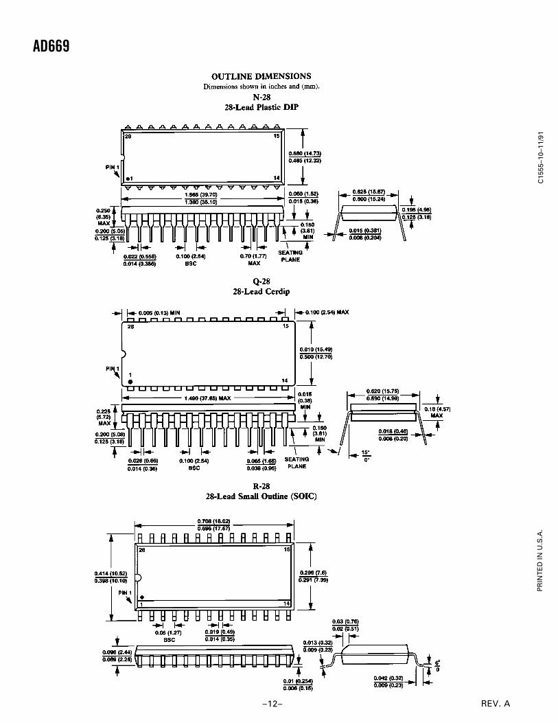
8-BIT MICROPROCESSOR INTERFACEThe AD669 can easily be operated with an 8-bit bus by the ad-dition of an octal latch. The 16-bit first rank register is loadedfrom the 8-bit bus as two bytes. Figure 11 shows the configura-tion when using a 74HC573 octal latch.
The eight most significant bits are latched into the 74HC573 bysetting the “latch enable” control line low. The eight least sig-nificant bits are then placed onto the bus. Now all sixteen bitscan be simultaneously loaded into the first rank register of theAD669 by setting CS and L1 low.
8-BIT µPAND
CONTROL
D7
D0
D7
D0
Q7
Q0
74HC573
11LDAC
MSB
DB8
DB7
LSB
AD669
CS1 L1
Figure 11. Connections for 8-Bit Bus Interface
AD669
REV. A –11–
NOISEIn high resolution systems, noise is often the limiting factor. A16-bit DAC with a 10 volt span has an LSB size of 153 µV(–96 dB). Therefore, the noise floor must remain below thislevel in the frequency range of interest. The AD669’s noisespectral density is shown in Figures 12 and 13. Figure 12 showsthe DAC output noise voltage spectral density for a 20 V spanexcluding the reference. This figure shows the l/f corner frequencyat 100 Hz and the wideband noise to be below 120 nV/√Hz.Figure 13 shows the reference noise voltage spectral density.This figure shows the reference wideband noise to be below125 nV/√Hz.
1000
11 1M
100
10
10 100k10k1k100 10M
FREQUENCY – Hz
NO
ISE
VO
LT
AG
E –
nV
/ H
z
Figure 12. DAC Output Noise Voltage Spectral Density
1000
11 1M
100
10
10 100k10k1k100 10M
FREQUENCY – Hz
NO
ISE
VO
LT
AG
E –
nV
/ H
z
Figure 13. Reference Noise Voltage Spectral Density
BOARD LAYOUTDesigning with high resolution data converters requires carefulattention to board layout. Trace impedance is the first issue. A306 µA current through a 0.5 Ω trace will develop a voltagedrop of 153 µV, which is 1 LSB at the 16-bit level for a 10 Vfull-scale span. In addition to ground drops, inductive and ca-pacitive coupling need to be considered, especially when highaccuracy analog signals share the same board with digital sig-nals. Finally, power supplies need to be decoupled in order tofilter out ac noise.
Analog and digital signals should not share a common path.Each signal should have an appropriate analog or digital returnrouted close to it. Using this approach, signal loops enclose asmall area, minimizing the inductive coupling of noise. Wide PCtracks, large gauge wire, and ground planes are highly recom-mended to provide low impedance signal paths. Separate analogand digital ground planes should also be utilized, with a singleinterconnection point to minimize ground loops. Analog signalsshould be routed as far as possible from digital signals andshould cross them at right angles.
One feature that the AD669 incorporates to help the user layoutis the analog pins (VCC, VEE, REF OUT, REF IN, SPAN/BIPOFFSET, VOUT and AGND) are adjacent to help isolate analogsignals from digital signals.
SUPPLY DECOUPLINGThe AD669 power supplies should be well filtered, well regu-lated, and free from high frequency noise. Switching power sup-plies are not recommended due to their tendency to generatespikes which can induce noise in the analog system.
Decoupling capacitors should be used in very close layout prox-imity between all power supply pins and ground. A 10 µF tanta-lum capacitor in parallel with a 0.1 µF ceramic capacitorprovides adequate decoupling. VCC and VEE should be bypassedto analog ground, while VLL should be decoupled to digitalground.
An effort should be made to minimize the trace length betweenthe capacitor leads and the respective converter power supplyand common pins. The circuit layout should attempt to locatethe AD669, associated analog circuitry and interconnections asfar as possible from logic circuitry. A solid analog ground planearound the AD669 will isolate large switching ground currents.For these reasons, the use of wire wrap circuit constructionis not recommended; careful printed circuit construction ispreferred.
GROUNDINGThe AD669 has two pins, designated analog ground (AGND)and digital ground (DGND.) The analog ground pin is the“high quality” ground reference point for the device. Any exter-nal loads on the output of the AD669 should be returned toanalog ground. If an external reference is used, this should alsobe returned to the analog ground.
If a single AD669 is used with separate analog and digitalground planes, connect the analog ground plane to AGND andthe digital ground plane to DGND keeping lead lengths as shortas possible. Then connect AGND and DGND together at theAD669. If multiple AD669s are used or the AD669 shares ana-log supplies with other components, connect the analog anddigital returns together once at the power supplies rather than ateach chip. This single interconnection of grounds prevents largeground loops and consequently prevents digital currents fromflowing through the analog ground.
AD669
REV. A–12–
C1
55
5–1
0–1
1/9
1P
RIN
TE
D I
N U
.S.A
.