adp1829, apd210x and adp171x reference design … apd210x and adp171x reference design preliminary...
TRANSCRIPT

ADP1829, APD210X and ADP171X Reference Design
Preliminary Technical Data FCDC 00057
Rev. A Reference designs are as supplied “as is” and without warranties of any kind, express, implied, or statutory including, but not limited to, any implied warranty of merchantability or fitness for a particular purpose. No license is granted by implication or otherwise under any patents or other intellectual property by application or use of reference designs. Information furnished by Analog Devices is believed to be accurate and reliable. However, no responsibility is assumed by Analog Devices for its use, nor for any infringements of patents or other rights of third parties that may result from its use. Analog Devices reserves the right to change devices or specifications at any time without notice. Trademarks and registered trademarks are the property of their respective owners. Reference designs are not authorized to be used in life support devices or systems.
One Technology Way, P.O. Box 9106, Norwood, MA 02062-9106, U.S.A. Tel: 781.329.4700 www.analogFax: 781.461.3113 ©2007 Analog Devices, Inc. All rights rese
FEATURES Seven Output Voltages: 5.0 V, 3.6 V, 3.3 V, 2.5 V, 1.8 V, 1.2 V, 0.9 V Output Current: 0.002 A to 3.0 A Input voltage: 10.8-13.2 V Ripple 2% ppk of Output Voltage Transient step ±5%, 50% max load
ADP1829, APD210X AND ADP171X REFERENCE DESIGN DESCRIPTION
This ADP1829, APD210X and ADP171X Reference Design uses 10.8 V to 13.2 V for the input voltage. The output voltages and currents are as follows:
• VOUT1 = 3.6 V with a maximum output current of 7.7 A for intermediate rail,
• VOUT2 = 1.2 V with a maximum output current of 3.0 A for VP,
• VOUT3 = 1.8 V with a maximum output current of 2.8 A for VP,
• VOUT4 = 0.9 V with a maximum output current of +/-0.5 A for VP,
• VOUT5 = 3.3 V with a maximum output current of 0.34 A for VP,
• VOUT6 = 1.2 V with a maximum output current of 0.1 A for VP,
• VOUT7 = 3.3 V with a maximum output current of 1.5 A for FPGA,
• VOUT8 = 2.5 V with a maximum output current of 1.6 A for FPGA,
• VOUT9 = 1.8 V with a maximum output current of 1.6 A for FPGA,
• VOUT10 = 1.2 V with a maximum output current of 0.5 A for FPGA,
• VOUT11 = 2.5 V with a maximum output current of 0.3 A for FPGA,
• VOUT12 = 1.8 V with a maximum output current of 1.95 A for DVI,
• VOUT13 = 0.9 V with a maximum output current of +/-0.5 A for FPGA,
• VOUT14 = 3.3 V with a maximum output current of 1.55 A for DVI,
• VOUT15 = 5.0 V with a maximum output current of 0.005 A for DVI,
• VOUT16 = 3.3 V with a maximum output current of 0.6 A for DCD,
• VOUT17 = 1.8 V with a maximum output current of 0.9 A for DCD,
• VOUT18 = 3.3 V with a maximum output current of 0.02 A for DCD,
• VOUT19 = 2.5 V with a maximum output current of 0.4 A for DCD,
• VOUT20 = 1.25 V with a maximum output current of 0.002 A for DCD,

Preliminary Technical Data FCDC 00057
Rev. A | Page 2 of 18
Design criteria are for coincidental tracking of VOUT17 and VOUT19 with VOUT16 and near ratiometric tracking of VOUT2 with VOUT5 to ensure turn on times are nearly the same (VOUT5 reaches regulation no more than 500us after VOUT2 ). Two DDR terminations are designed for ratiometric tracking: VOUT4 tracks VOUT3 and VOUT13 tracks VOUT9 . All outputs discharge to 0.1 V in under 100 ms through external pull down resistors switched on when the rails are disabled. The ripple and transient assumptions are 2% peak to peak voltage ripple (for the switchers) and 5% deviation due to 50% instantaneous load step respectively. The nominal switching frequency is fixed at 300 kHz for VOUT1, VOUT2, VOUT3 VOUT4 VOUT12 and VOUT13. VOUT7, VOUT8, VOUT9 VOUT14 VOUT16 and VOUT17 switch at a fixed nominal frequency of 1.2 MHz. VOUT10 switches at a pseudo fixed frequency of 3 MHz (frequency varies slightly with load). All other outputs are filtered, or linear regulated out of the switching rails.
Preliminary Technical Data FCDC 00057
Rev. A | Page 3 of 18
TABLE OF CONTENTS Features....................................................................................................................................................................................................... 1 ADP1829, APD210X and ADP171X Reference Design Description ................................................................................................ 1 Revision History........................................................................................................................................................................................ 3 General Description ................................................................................................................................................................................. 4
ADP1823................................................................................................................................................................................................ 4 ADP2105, ADP2106, ADP2107.......................................................................................................................................................... 4 ADP171X ............................................................................................................................................................................................... 4
Block Diagram........................................................................................................................................................................................... 4 Schematic ................................................................................................................................................................................................... 6 Bill of Materials ....................................................................................................................................................................................... 12
TABLE OF FIGURES Figure 1. Block Diagram of the System ............................................................................................................................................ 5 Figure 2. Schematic: VOUT1 and VOUT2 ............................................................................................................................................... 6
Figure 3. Schematic: VOUT3 ,VOUT4 ,VOUT5 and VOUT6 ....................................................................................................................... 7
Figure 4. Schematic: VOUT7 ,VOUT8 ,VOUT9 ,VOUT10 and VOUT11 ......................................................................................................... 8
Figure 5. Schematic: VOUT12 ,VOUT13 ,VOUT14 and VOUT15 .................................................................................................................. 9
Figure 6. Schematic: VOUT16 ,VOUT17 ,VOUT18 ,VOUT19 and VOUT20 ................................................................................................... 10
Figure 7. Schematic: Power Down Circuitry ................................................................................................................................. 11
REVISION HISTORY 9/5/2007—Revision 0: Initial Version
Preliminary Technical Data FCDC 00057
Rev. A | Page 4 of 18
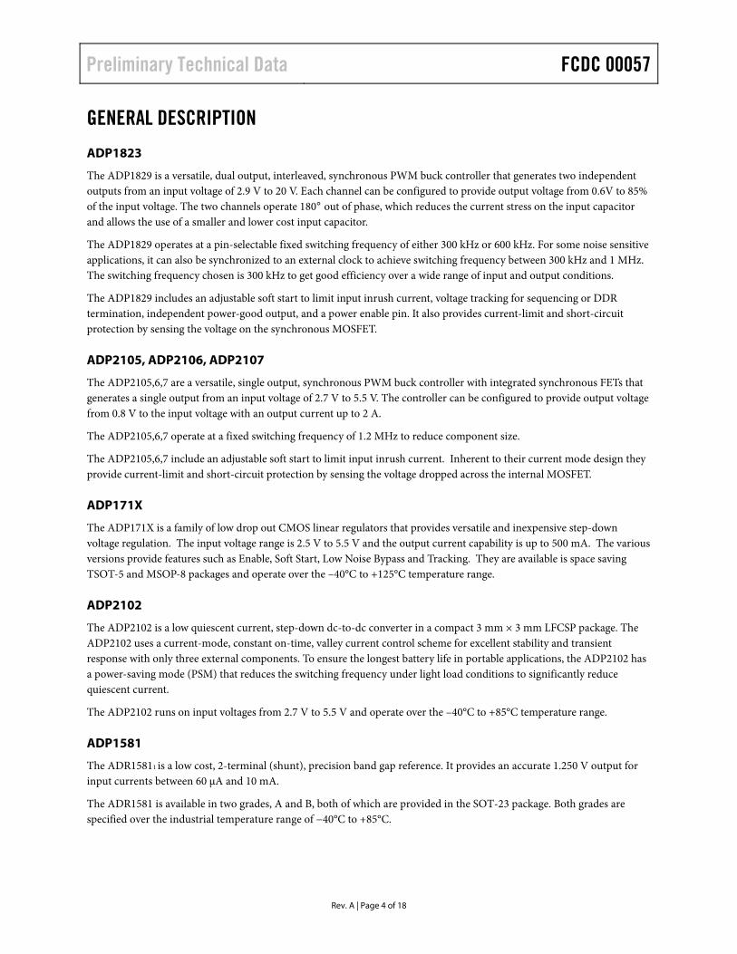
GENERAL DESCRIPTION
ADP1823
The ADP1829 is a versatile, dual output, interleaved, synchronous PWM buck controller that generates two independent outputs from an input voltage of 2.9 V to 20 V. Each channel can be configured to provide output voltage from 0.6V to 85% of the input voltage. The two channels operate 180° out of phase, which reduces the current stress on the input capacitor and allows the use of a smaller and lower cost input capacitor.
The ADP1829 operates at a pin-selectable fixed switching frequency of either 300 kHz or 600 kHz. For some noise sensitive applications, it can also be synchronized to an external clock to achieve switching frequency between 300 kHz and 1 MHz. The switching frequency chosen is 300 kHz to get good efficiency over a wide range of input and output conditions.
The ADP1829 includes an adjustable soft start to limit input inrush current, voltage tracking for sequencing or DDR termination, independent power-good output, and a power enable pin. It also provides current-limit and short-circuit protection by sensing the voltage on the synchronous MOSFET.
ADP2105, ADP2106, ADP2107
The ADP2105,6,7 are a versatile, single output, synchronous PWM buck controller with integrated synchronous FETs that generates a single output from an input voltage of 2.7 V to 5.5 V. The controller can be configured to provide output voltage from 0.8 V to the input voltage with an output current up to 2 A.
The ADP2105,6,7 operate at a fixed switching frequency of 1.2 MHz to reduce component size.
The ADP2105,6,7 include an adjustable soft start to limit input inrush current. Inherent to their current mode design they provide current-limit and short-circuit protection by sensing the voltage dropped across the internal MOSFET.
ADP171X
The ADP171X is a family of low drop out CMOS linear regulators that provides versatile and inexpensive step-down voltage regulation. The input voltage range is 2.5 V to 5.5 V and the output current capability is up to 500 mA. The various versions provide features such as Enable, Soft Start, Low Noise Bypass and Tracking. They are available is space saving TSOT-5 and MSOP-8 packages and operate over the –40°C to +125°C temperature range.
ADP2102
The ADP2102 is a low quiescent current, step-down dc-to-dc converter in a compact 3 mm × 3 mm LFCSP package. The ADP2102 uses a current-mode, constant on-time, valley current control scheme for excellent stability and transient response with only three external components. To ensure the longest battery life in portable applications, the ADP2102 has a power-saving mode (PSM) that reduces the switching frequency under light load conditions to significantly reduce quiescent current.
The ADP2102 runs on input voltages from 2.7 V to 5.5 V and operate over the –40°C to +85°C temperature range.
ADP1581
The ADR15811 is a low cost, 2-terminal (shunt), precision band gap reference. It provides an accurate 1.250 V output for input currents between 60 μA and 10 mA.
The ADR1581 is available in two grades, A and B, both of which are provided in the SOT-23 package. Both grades are specified over the industrial temperature range of −40°C to +85°C.

Preliminary Technical Data FCDC 00057
Rev. A | Page 5 of 18
BLOCK DIAGRAM
Figure 1. Block Diagram of the System

Preliminary Technical Data FCDC 00057
Rev. A | Page 6 of 18
SCHEMATIC
Figure 2. Schematic: VOUT1
and VOUT2

Preliminary Technical Data FCDC 00057
Rev. A | Page 7 of 18
12Vin
Cb3
Csn3Rsn3
L3Rlim3
Cpv3
Cc32Rc32
Rf31
Db3
QH3
QL3
Co31 Co32
Cc30
Cc31 Rc31
Cin31
Cb4
Rsn4
L4Rlim4Db4
QH4
QL4
Co41 Co42
Cin41Rf42
Cc42Rc42
Rf41
Cc40
Cc41Rc41
1V8_VP
0V9_VPCss4
Css3 Cbias3
Csn4
Rf32
Rpg3
Rin3
Clim3
Clim4
Rf43
Rpg4
POK1V8
POK0V9_VP
Rpv3
Cvcc3
1.8V at 2.8A (VP) and 0.9V at +/-0.5A (VP)
ADP1829ACPZ
1
2
3
4
5
6
7
8
9 10 11 12 13 14 15 16
17
18
19
20
21
22
23
24
26 25272829303132
SS2 POK2 BST2 DH2 SW2 CSL2 PGND2 DL2
PV
DL1
PGND1
CSL1
SW1
DH1
BST1
POK1
EN1EN2LDOSD
INVREGSS1TRK1CMP1
FB1
SYNC
FREQ
GND
UV2
FB2
CMP2
TRK2
Rt42
Rt41
1V8_VP
POK3V6
Rf52
Rf51
3V3_VP
Css5Co51
Cin51
Vo3V6 EN
4 5
1 8
GNDIN
OUT GND
GND
GND
SS/ADJ
ADP1715
3.3V at 0.34A (VP) and 1.2V at 0.1A (VP)
Cin61 Co61
1V2_VP_LVo3V6
ADP1710
NC3 4
1 5
GND
EN
OUTIN
U3
U5
U6
POK3V6
POK3V6
Figure 3. Schematic: VOUT3
,VOUT4
,VOUT5
and VOUT6

Preliminary Technical Data FCDC 00057
Rev. A | Page 8 of 18
L7
Cin71
Cin72
Rc71
Rin7Cvcc7
3V3_FPGA
Co71
Rf72
Cc70
Rf71
Cc71
Css7
Vo3V6
POK3V6
3.3V at 1.5A (FPGA) and 2.5V at 1.6A (FPGA)
1
L8
Cin81
Cin82
Rc81
Rin8Cvcc8
2V5_FPGA
Co81
Rf82
Cc80
Rf81
Cc81
Css8
Vo3V6
POK3V61
1.8V at 1.6A (FPGA) and 1.2V at 0.5A (FPGA)
L9
Cin91
Cin92
Rc91
Rin9Cvcc9
1V8_FPGA
Co91
Rf92
Cc90
Rf91
Cc91
Css9
Vo3V6
POK3V61
U9
en
59
16 13
gnd
gnd
gndcmp ss agnd nc
pin2
pin1lx2
lx1
pgnd
avingndfb
ADP2107ACPZ1.8-R7
U7
en
59
16 13
gnd
gnd
gndcmp ss agnd nc
pin2
pin1lx2
lx1
pgnd
avingndfb
ADP2107ACPZ3.3-R7
U8
en
59
16 13
gnd
gnd
gndcmp ss agnd nc
pin2
pin1lx2
lx1
pgnd
avingndfb
ADP2107ACPZ-R7
MODE
4 5
1 8
PVINEN
FB_OUT LX
PGND
AVIN
AGND
ADP2102-1.2
Cvcc10
Cin101
L101V2_FPGA
Co101
U10POK3V6
Vo3V6
Rin10
2.5V at 0.3A (FPGA) Low Noise
Cin111 Co111
Css11
U11ADJ/SS3 4
1 5
GND
EN
OUTINADP1712AUJZ-2.5
Vo3V6 2V5_FPGA_L
POK3V6
Figure 4. Schematic: VOUT7
,VOUT8
,VOUT9
,VOUT10
and VOUT11

Preliminary Technical Data FCDC 00057
Rev. A | Page 9 of 18
12Vin
Cb12
Csn12Rsn12
L12Rlim12
Cpv12
Cc122Rc122
Rf121
Db12
QH12
QL12
Co121 Co122
Cc120
Cc121 Rc121
Cin121
Cb13
Rsn13
L13Rlim13Db13
QH13
QL13
Co131 Co132
Cin131Rf132
Cc132Rc132
Rf131
Cc130
Cc131Rc131
1V8_DVI
0V9_FPGACss13
Css12 Cbias12
Csn13
Rf122
Rpg12
Rin12
Clim12
Clim13
Rf133
Rpg13
POK1V8_DVI
POK0V9_FPGA
Rpv12
Cvcc12
0.9V at +/-0.5A (FPGA) and 1.8V at 1.95A (DVI)
ADP1829ACPZ
1
2
3
4
5
6
7
8
9 10 11 12 13 14 15 16
17
18
19
20
21
22
23
24
26 25272829303132
SS2 POK2 BST2 DH2 SW2 CSL2 PGND2 DL2
PV
DL1
PGND1
CSL1
SW1
DH1
BST1
POK1
EN1EN2LDOSD
INVREGSS1TRK1CMP1
FB1
SYNC
FREQ
GND
UV2
FB2
CMP2
TRK2
Rt132
Rt131
1V8_FPGA
POK3V6
U12
Rt122
Rt121
3V3_DVI
3.3V at 1.55A (DVI)
5V0_DVICo151
Rout15
L14
Cin141
Cin142
Rc141
Rin14Cvcc14
3V3_DVI
Co141
Rf142
Cc140
Rf141
Cc141
Css14
Vo3V6
POK3V61
U14
en
59
16 13
gnd
gnd
gndcmp ss agnd nc
pin2
pin1lx2
lx1
pgnd
avingndfb
ADP2107ACPZ3.3-R7
1V8_FPGA
Figure 5. Schematic: VOUT12
,VOUT13
,VOUT14
and VOUT15

Preliminary Technical Data FCDC 00057
Rev. A | Page 10 of 18
Figure 6. Schematic: VOUT16
,VOUT17
,VOUT18
,VOUT19
and VOUT20

Preliminary Technical Data FCDC 00057
Rev. A | Page 11 of 18
POK3V6
Roff
Qoff
Pull Down Circuitry Ensures all rails <0.1V in under 100ms from ON deassertion
12Vin
Vo3V6
1V2_VP
1V8_VP
0V9_VP
3V3_VP
1V2_VP_L
3V3_FPGA
2V5_FPGA
1V8_FPGA
1V2_FPGA
2V5_FPGA_L
1V8_DVI
0V9_FPGA
3V3_DVI
5V0_DVI
3V3_DCD
1V8_DCD
2V5_DCD
Rp1
Qp1
Rp3
Qp3
Rp2
Qp2
Rp4
Qp4
Rp5
Qp5
Rp7
Qp7
Rp6
Qp6
Rp8
Qp8
Rp9
Qp9
Rp11
Qp11
Rp10
Qp10
Rp12
Qp12
Rp13
Qp13
Rp15
Qp15
Rp14
Qp14
Rp16
Qp16
Rp17
Qp17Rp19
Qp19
Figure 7. Schematic: Power Down Circuitry

Preliminary Technical Data FCDC 00057
Rev. A | Page 12 of 18
BILL OF MATERIALS Table 1. Vout1, and Vout2 Bill of Materials (Vo3V6 and 1V2_VP)
Description Designator Quantity Manufacturer MFR# Capacitor Ceramic X7R 2.2n 0603 50V Cc12 1 Vishay Generic Capacitor Ceramic COG 22p 0603 50V Cc10, Cc20 2 Vishay Generic Capacitor Ceramic X7R 1.8n 0603 50V Cc11 1 Vishay Generic Capacitor Ceramic X7R 1u 0603 16V Cbias1, Cpv1, Cvcc1 3 Murata GRM188R71C105KA12D Capacitor Ceramic X7R 47n 0603 16V Css1 1 Vishay Generic Capacitor Ceramic X7R 4.7n 0603 50V Css2 1 Vishay Generic Capacitor Ceramic X5R 22u 1210 16V Cin11, Cin21 2 Murata grm32er61c226k Capacitor Al Poly 125C 180u 10mm x 7.7mm 16V Cin12 1 Nippon Chemi-con APXH160ARA181MJ80G Capacitor Ceramic X7R 100n 0603 16V Cb1, Cb2 2 Vishay Generic Capacitor Ceramic COG 33p 0603 50V Clim1, Clim2 2 Vishay Generic Capacitor Ceramic X7R 1.5n 0603 50V Cc21 1 Vishay Generic Capacitor Ceramic X7R 1.2n 0603 50V Cc22 1 Vishay Generic Capacitor Ceramic X5R 22u 1206 6.3V Co11, Co21 2 Murata grm31cr60j226k Capacitor Al Poly 105C 470u 8mm x 7.7mm 6.3V Co12 1 Nippon Chemi-con APXE6R3ARA471MH80G Capacitor Al Poly 105C 180u 5mm x 5.8mm 2.5V Co22 1 Nippon Chemi-con APXE2R5ARA181ME61G Diode Schottky 200mA SOD-323 30V Db1, Db2 2 Diodes inc BAT54WS Inductor Iron 4.5uH 13.2mm x 13.8mm L1 1 Coilcraft MLC1550-452MLC Inductor Ferrite 3.8uH 10.2mm x 10mm L2 1 Coilcraft MSS1038-382NLC Single N-Channel MOSFET PG-TDSON-8 30V QH1, QH2 2 Infineon BSC120N03LS Single N-Channel MOSFET PG-TDSON-8 30V QL1, QL2 2 Infineon BSC050N03LS 5% Thick Film 10 Ohms 0603 Rpv1, Rin1, Rf23 3 Vishay Generic 1% Thick Film 3.92k 0603 Rf12 1 Vishay Generic 1% Thick Film 10.0k 0603 Rpg1, Rpg2 2 Vishay Generic
1% Thick Film 20.0k 0603 Rf11, Rf21, Rf22, Rt21 4 Vishay Generic
1% Thick Film 5.36k 0603 Rt22 1 Vishay Generic 1% Thick Film 3.24k 0603 Rc22 1 Vishay Generic 1% Thick Film 1.18k 0603 Rlim1 1 Vishay Generic 1% Thick Film 2.43k 0603 Rlim2 1 Vishay Generic 1% Thick Film 2.87k 0603 Rc12 1 Vishay Generic 1% Thick Film 24.9k 0603 Rc11 1 Vishay Generic 1% Thick Film 18.7k 0603 Rc21 1 Vishay Generic 2 chan 300k to 600k PWM LFCSP-32 U1 1 Analog Devices ADP1829ACPZ

Preliminary Technical Data FCDC 00057
Rev. A | Page 13 of 18
Table 2. Vout3, Vout4, Vout5 and Vout6 Bill of Materials (3V3_VP, 1V8_VP, 1V2_VP and 0V9_VP)
Description Designator Quantity Manufacturer MFR# Capacitor Ceramic COG 22p 0603 50V Cc30, Cc40 2 Vishay Generic Capacitor Ceramic X7R 1.8n 0603 50V Cc31, Cc32 2 Vishay Generic
Capacitor Ceramic X7R 1u 0603 16V Cbias3, Cpv3, Cvcc3, Cin61, Co61 5 Murata GRM188R71C105KA12D
Capacitor Ceramic X7R 22n 0603 16V Css3 1 Vishay Generic Capacitor Ceramic X7R 4.7n 0603 50V Css4 1 Vishay Generic Capacitor Ceramic X7R 10n 0603 50V Css5 1 Vishay Generic Capacitor Ceramic X5R 22u 1210 16V Cin31 1 Murata grm32er61c226k Capacitor Ceramic X5R 2.2u 0805 16V Cin51, Co51 2 Murata GRM21BR61C225KA88L Capacitor Ceramic X7R 100n 0603 16V Cb3, Cb4 2 Vishay Generic Capacitor Ceramic COG 33p 0603 50V Clim3, Clim4 2 Vishay Generic Capacitor Ceramic COG 330p 0603 50V Cc41 1 Vishay Generic Capacitor Ceramic COG 820p 0603 50V Cc42 1 Vishay Generic Capacitor Ceramic X5R 22u 1206 6.3V Co31, Co41, Cin41 3 Murata grm31cr60j226k Capacitor Al Poly 105C 180u 5mm x 5.8mm 2.5V Co32 1 Nippon Chemi-con APXE2R5ARA181ME61G Diode Schottky 200mA SOD-323 30V Db3, Db4 2 Diodes inc BAT54WS Inductor Ferrite 7.0uH 10.2mm x 10mm L3 1 Coilcraft MSS1038-702NLC Inductor Ferrite 10uH 8mm x 8mm L4 1 Coilcraft MSS7341-103MLD Single N-Channel MOSFET PG-TDSON-8 30V QL3 1 Infineon BSC120N03LS Single N-Channel MOSFET SOT23-6 20V QH3, QH4, QL4 3 Vishay Si3460DV 5% Thick Film 10 Ohms 0603 Rpv3, Rin3 2 Vishay Generic 1% Thick Film 10.0k 0603 Rf32, Rpg3, Rpg4 3 Vishay Generic 1% Thick Film 4.99k 0603 Rf43 1 Vishay Generic 1% Thick Film 24.9k 0603 Rf42 1 Vishay Generic 1% Thick Film 15.0k 0603 Rf41 1 Vishay Generic 1% Thick Film 20.0k 0603 Rf31, Rt41 2 Vishay Generic 1% Thick Film 7.68k 0603 Rt42 1 Vishay Generic 1% Thick Film 60.4 Ohms 0603 Rc42 1 Vishay Generic 1% Thick Film 2.00k 0603 Rlim3 1 Vishay Generic 1% Thick Film 1.05k 0603 Rlim4 1 Vishay Generic 1% Thick Film 2.15k 0603 Rc32 1 Vishay Generic 1% Thick Film 21.5k 0603 Rc31 1 Vishay Generic 1% Thick Film 49.9k 0603 Rc41 1 Vishay Generic 2 chan 300k to 600k PWM LFCSP-32 U3 1 Analog Devices ADP1829ACPZ 500mA 2.5V Linear Reg MSOP-8 w/track U5 1 Analog Devices ADP1715ARMZ-3.3-R7 150mA 1.2V Linear Reg TSOT-5 U6 1 Analog Devices ADP1710AUJZ-1.2-R7

Preliminary Technical Data FCDC 00057
Rev. A | Page 14 of 18
Table 3. Vout7, Vout8, Vout9, Vout10 and Vout11 Bill of Materials (3V3_FPGA, 2V5_FPGA, 1V8_FPGA, 1V2_FPGA and 2V5_FPGA)
Description Designator Quantity Manufacturer MFR# Capacitor Ceramic X7R 1u 0603 16V Cin71, Cin72 2 Murata GRM188R71C105KA12D
Capacitor Ceramic X5R 2.2u 0805 16V Cin81, Cin82, Cin101, Cin111, Co111 5 Murata GRM21BR61C225KA88L
Capacitor Ceramic X5R 4.7u 0805 10V Cin91, Cin92, Cout101 3 Murata GRM21BR61A475KA73L Capacitor Ceramic X7R 1n 0603 50V Css7, Css8, Css9 3 Vishay Generic Capacitor Ceramic X7R 10n 0603 25V Css11 1 Vishay Generic Capacitor Ceramic COG 82p 0603 50V Cc71 1 Vishay Generic Capacitor Ceramic COG 68p 0603 50V Cc91 1 Vishay Generic
Capacitor Ceramic X7R 100n 0603 16V Cvcc7, Cvcc8, Cvcc9, Cvcc10 4 Vishay Generic
Capacitor Ceramic COG 120p 0603 50V Cc81 1 Vishay Generic Capacitor Ceramic X5R 10u 1206 10V Co71, Co81 2 Murata grm31mr61a106k Capacitor Ceramic X5R 22u 1206 6.3V Co91 1 Murata grm31cr60j226k Inductor Ferrite 3.3uH 4mm x 4mm L7 1 Coilcraft LPS4018-332 Inductor Ferrite 2.2uH 4mm x 4mm L8, L9 2 Coilcraft LPS4018-222 Inductor Ferrite 2.2uH 1210 1.1A L10 1 Taiyo Yuden CB C3225T2R2MR 5% Thick Film 10 Ohms 0603 Rin7, Rin8, Rin9, Rin10 4 Vishay Generic 1A Thick Film 0 Ohm jumper 0603 Rf71, Rf91 2 Vishay Generic 1% Thick Film 169k 0603 Rf81 1 Vishay Generic 1% Thick Film 80.6k 0603 Rf82 1 Vishay Generic 1% Thick Film 69.8k 0603 Rc81 1 Vishay Generic 1% Thick Film 100k 0603 Rc71 1 Vishay Generic 1% Thick Film 200k 0603 Rc91 1 Vishay Generic Integrated 1.2MHz PWM LFCSP-16 U7 1 Analog Devices ADP2107ACPZ-3.3-R7 Integrated 1.2MHz PWM LFCSP-16 U8 1 Analog Devices ADP2107ACPZ-R7 Integrated 1.2MHz PWM LFCSP-16 U9 1 Analog Devices ADP2107ACPZ-1.8-R7 Integrated 3MHz PWM LFCSP-8 U10 1 Analog Devices ADP2102YCPZ-1.2-R7 300mA 2.5V Linear Reg TSOT-5 w/SS U11 1 Analog Devices ADP1712AUJZ-2.5-R7
Preliminary Technical Data FCDC 00057
Rev. A | Page 15 of 18
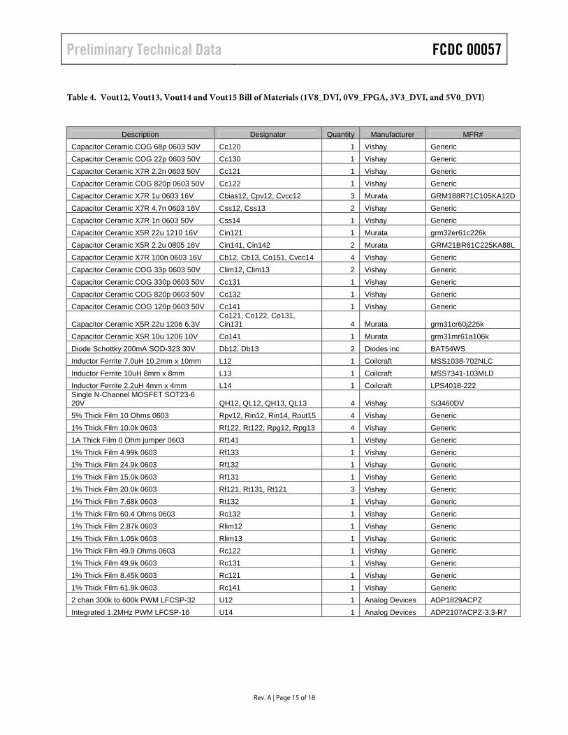
Table 4. Vout12, Vout13, Vout14 and Vout15 Bill of Materials (1V8_DVI, 0V9_FPGA, 3V3_DVI, and 5V0_DVI)
Description Designator Quantity Manufacturer MFR# Capacitor Ceramic COG 68p 0603 50V Cc120 1 Vishay Generic Capacitor Ceramic COG 22p 0603 50V Cc130 1 Vishay Generic Capacitor Ceramic X7R 2.2n 0603 50V Cc121 1 Vishay Generic Capacitor Ceramic COG 820p 0603 50V Cc122 1 Vishay Generic Capacitor Ceramic X7R 1u 0603 16V Cbias12, Cpv12, Cvcc12 3 Murata GRM188R71C105KA12D Capacitor Ceramic X7R 4.7n 0603 16V Css12, Css13 2 Vishay Generic Capacitor Ceramic X7R 1n 0603 50V Css14 1 Vishay Generic Capacitor Ceramic X5R 22u 1210 16V Cin121 1 Murata grm32er61c226k Capacitor Ceramic X5R 2.2u 0805 16V Cin141, Cin142 2 Murata GRM21BR61C225KA88L Capacitor Ceramic X7R 100n 0603 16V Cb12, Cb13, Co151, Cvcc14 4 Vishay Generic Capacitor Ceramic COG 33p 0603 50V Clim12, Clim13 2 Vishay Generic Capacitor Ceramic COG 330p 0603 50V Cc131 1 Vishay Generic Capacitor Ceramic COG 820p 0603 50V Cc132 1 Vishay Generic Capacitor Ceramic COG 120p 0603 50V Cc141 1 Vishay Generic
Capacitor Ceramic X5R 22u 1206 6.3V Co121, Co122, Co131, Cin131 4 Murata grm31cr60j226k
Capacitor Ceramic X5R 10u 1206 10V Co141 1 Murata grm31mr61a106k Diode Schottky 200mA SOD-323 30V Db12, Db13 2 Diodes inc BAT54WS Inductor Ferrite 7.0uH 10.2mm x 10mm L12 1 Coilcraft MSS1038-702NLC Inductor Ferrite 10uH 8mm x 8mm L13 1 Coilcraft MSS7341-103MLD Inductor Ferrite 2.2uH 4mm x 4mm L14 1 Coilcraft LPS4018-222 Single N-Channel MOSFET SOT23-6 20V QH12, QL12, QH13, QL13 4 Vishay Si3460DV 5% Thick Film 10 Ohms 0603 Rpv12, Rin12, Rin14, Rout15 4 Vishay Generic 1% Thick Film 10.0k 0603 Rf122, Rt122, Rpg12, Rpg13 4 Vishay Generic 1A Thick Film 0 Ohm jumper 0603 Rf141 1 Vishay Generic 1% Thick Film 4.99k 0603 Rf133 1 Vishay Generic 1% Thick Film 24.9k 0603 Rf132 1 Vishay Generic 1% Thick Film 15.0k 0603 Rf131 1 Vishay Generic 1% Thick Film 20.0k 0603 Rf121, Rt131, Rt121 3 Vishay Generic 1% Thick Film 7.68k 0603 Rt132 1 Vishay Generic 1% Thick Film 60.4 Ohms 0603 Rc132 1 Vishay Generic 1% Thick Film 2.87k 0603 Rlim12 1 Vishay Generic 1% Thick Film 1.05k 0603 Rlim13 1 Vishay Generic 1% Thick Film 49.9 Ohms 0603 Rc122 1 Vishay Generic 1% Thick Film 49.9k 0603 Rc131 1 Vishay Generic 1% Thick Film 8.45k 0603 Rc121 1 Vishay Generic 1% Thick Film 61.9k 0603 Rc141 1 Vishay Generic 2 chan 300k to 600k PWM LFCSP-32 U12 1 Analog Devices ADP1829ACPZ Integrated 1.2MHz PWM LFCSP-16 U14 1 Analog Devices ADP2107ACPZ-3.3-R7

Preliminary Technical Data FCDC 00057
Rev. A | Page 16 of 18
Table 5. Vout16, Vout17, Vout18, Vout19 and Vout20 Bill of Materials (3V3_DCD, 1V8_DCD, 3V3_DCD_L, 2V5_DCD and 1V25_DCD_L)
Description Designator Quantity Manufacturer MFR# Capacitor Ceramic X7R 1u 0603 16V Cin161, Co162 2 Murata GRM188R71C105KA12D
Capacitor Ceramic X5R 2.2u 0805 16V Cin171, Cin172, Cin191, Co191 4 Murata GRM21BR61C225KA88L
Capacitor Ceramic X7R 1n 0603 50V Css16, Co201 2 Vishay Generic Capacitor Ceramic COG 100p 0603 50V Cc171, Css17 2 Vishay Generic
Capacitor Ceramic X7R 100n 0603 16V Cvcc16, Cvcc17, Co181 3 Vishay Generic
Capacitor Ceramic COG 47p 0603 50V Cc161 1 Vishay Generic Capacitor Ceramic X5R 22u 1206 6.3V Co161 1 Murata grm31cr60j226k Capacitor Ceramic X5R 10u 1206 10V Co171 1 Murata grm31mr61a106k Capacitor Al Poly 105C 100u 5mm x 5.8mm 4V Co182 1 Nippon Chemi-con APXE4R0ARA101ME61G Inductor Ferrite 4.7uH 1210 1A L16 1 Taiyo Yuden CB C3225T4R7MR Inductor Ferrite 2.2uH 1210 1.1A L17 1 Taiyo Yuden CB C3225T2R2MR Inductor Ferrite 100uH 1210 0.27A L18 1 Taiyo Yuden CB C3225T101MR 5% Thick Film 10 Ohms 0603 Rin16, Rin17, Rin18 3 Vishay Generic 1% Thick Film 402 Ohms 0603 Rin20 1 Vishay Generic 1A Thick Film 0 Ohm jumper 0603 Rf161, Rf171 2 Vishay Generic 1% Thick Film 100k 0603 Rt171 1 Vishay Generic 1% Thick Film 80.6k 0603 Rt172 1 Vishay Generic 1% Thick Film 200k 0603 Rc161 1 Vishay Generic 1% Thick Film 76.8k 0603 Rc171 1 Vishay Generic Diode Dual Schottky 200mA SOT-323 30V D18 1 Diodes inc BAT54SW Integrated 1.2MHz PWM LFCSP-16 U16 1 Analog Devices ADP2105ACPZ-3.3-R7 Integrated 1.2MHz PWM LFCSP-16 U17 1 Analog Devices ADP2105ACPZ-1.8-R7 500mA 2.5V Linear Reg MSOP-8 w/track U19 1 Analog Devices ADP1716ARMZ-2.5-R7 10mA 1.25V Shunt Ref SOT23 U20 1 Analog Devices ADR1581ARTZ

Preliminary Technical Data FCDC 00057
Rev. A | Page 17 of 18
Table 6. Power Down Bill of Materials
Description Designator Quantit
y Manufacturer MFR#
Single N-Channel MOSFET SOT523 60V
Qoff, Qp1, Qp2, Qp3, Qp4, Qp5, Qp6, Qp7, Qp8, Qp9, Qp10, Qp11, Qp12, Qp13, Qp14, Qp15, Qp16, Qp17, Qp19 19 Diodes inc 2N7002T-7-F
1% Thick Film 10.0k 0603 Roff 1 Vishay Generic 1% Thick Film 28.7 Ohms 1206 Rp1 1 Vishay Generic 1% Thick Film 130 Ohms 0603 Rp2 1 Vishay Generic 1% Thick Film 100 Ohms 0603 Rp3 1 Vishay Generic 1% Thick Film 1.43k 0603 Rp4, Rp13 2 Vishay Generic 1% Thick Film 9.09k 0603 Rp5 1 Vishay Generic 1% Thick Film 28.0k 0603 Rp6 1 Vishay Generic 1% Thick Film 1.96k 0603 Rp7, Rp14 2 Vishay Generic 1% Thick Film 2.15k 0603 Rp8 1 Vishay Generic 1% Thick Film 536 Ohms 0603 Rp9 1 Vishay Generic 1% Thick Film 5.90k 0603 Rp10 1 Vishay Generic 1% Thick Film 9.76k 0603 Rp11, Rp19 2 Vishay Generic 1% Thick Film 536 Ohms 0603 Rp12 1 Vishay Generic 1% Thick Film 178k 0603 Rp15 1 Vishay Generic 1% Thick Film 154 Ohms 0603 Rp16 1 Vishay Generic 1% Thick Film 2.37k 0603 Rp17 1 Vishay Generic

Preliminary Technical Data FCDC 00057
Rev. A | Page 18 of 18
NOTES
©2007 Analog Devices, Inc. All rights reserved. Trademarks and registered trademarks are the property of their respective owners. EB