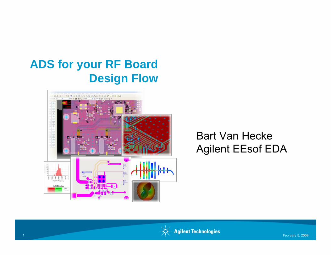
ads for your rf board design flow -...
TRANSCRIPT
February 5, 20091
Bart Van HeckeAgilent EEsof EDA
ADS for your RF Board Design Flow
February 5, 20092
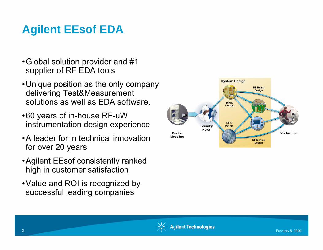
Agilent EEsof EDA
•Global solution provider and #1 supplier of RF EDA tools
•Unique position as the only company delivering Test&Measurement solutions as well as EDA software.
•60 years of in-house RF-uWinstrumentation design experience
•A leader for in technical innovation for over 20 years
•Agilent EEsof consistently ranked high in customer satisfaction
•Value and ROI is recognized by successful leading companies
February 5, 20093
Pric
e
Breadth & Capability
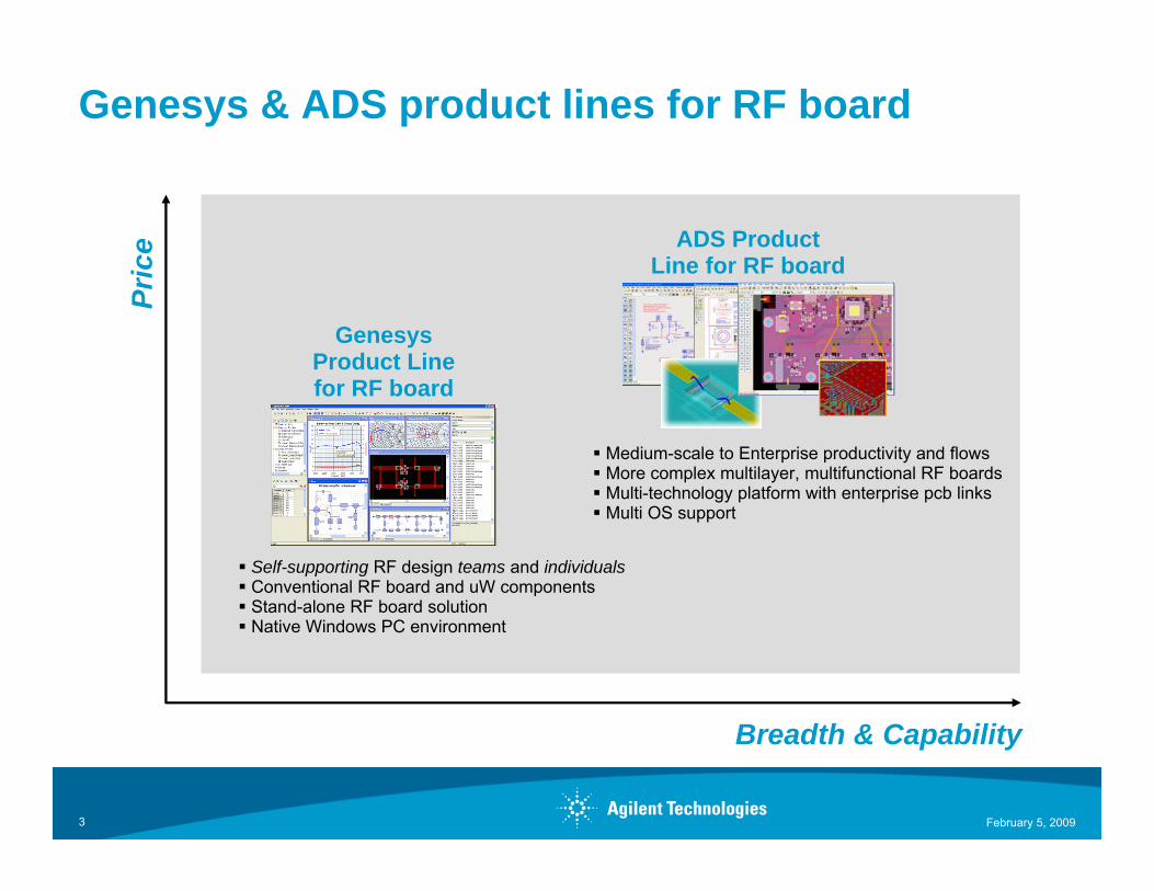
GenesysProduct Line for RF board
ADS Product Line for RF board
Self-supporting RF design teams and individualsConventional RF board and uW componentsStand-alone RF board solutionNative Windows PC environment
Medium-scale to Enterprise productivity and flowsMore complex multilayer, multifunctional RF boardsMulti-technology platform with enterprise pcb linksMulti OS support
Genesys & ADS product lines for RF board
February 5, 20094
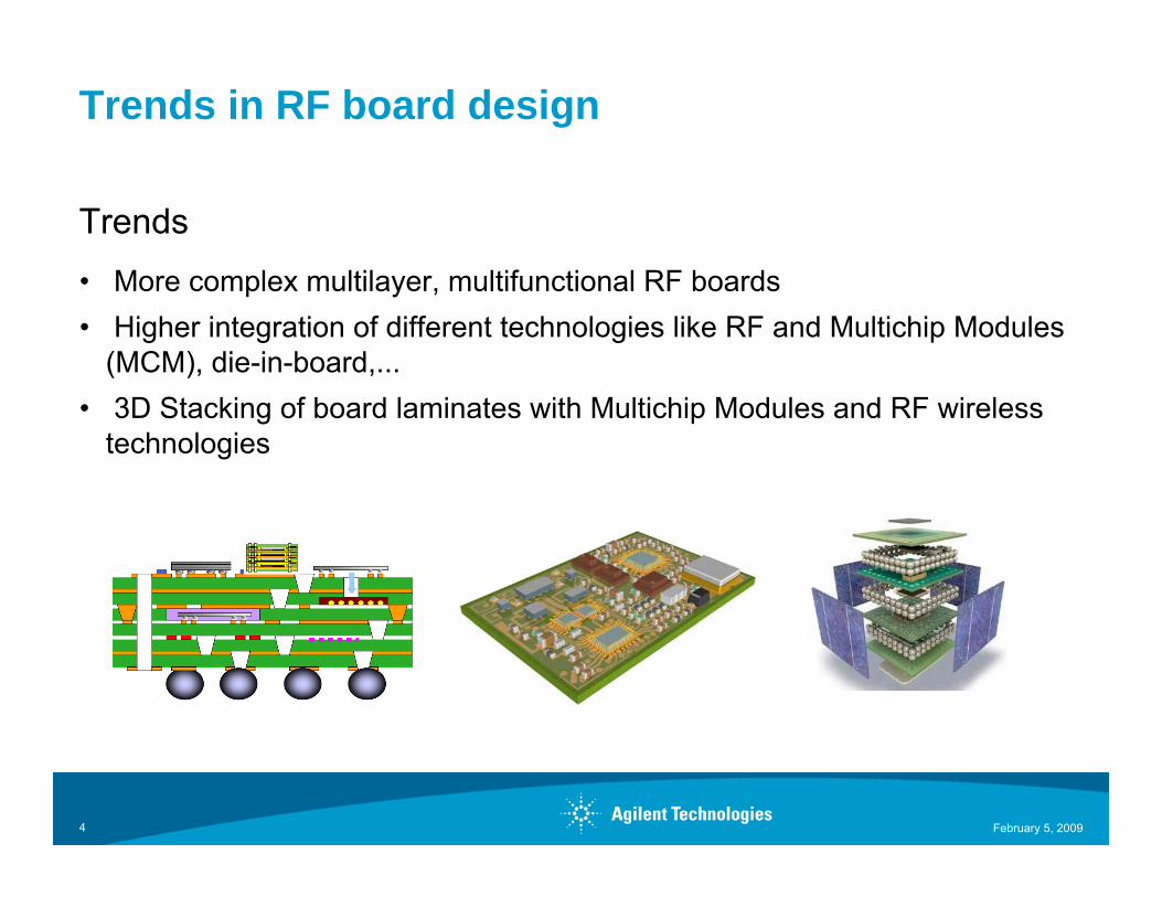
Trends in RF board design
Trends• More complex multilayer, multifunctional RF boards• Higher integration of different technologies like RF and Multichip Modules
(MCM), die-in-board,...• 3D Stacking of board laminates with Multichip Modules and RF wireless
technologies
February 5, 20095
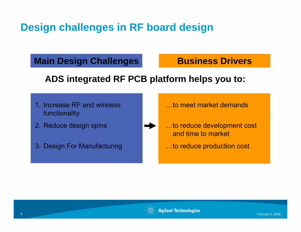
1. Increase RF and wireless functionality
2. Reduce design spins
3. Design For Manufacturing
Main Design Challenges Business Drivers
ADS integrated RF PCB platform helps you to:
Design challenges in RF board design
…to meet market demands
…to reduce development cost and time to market
…to reduce production cost
February 5, 20096
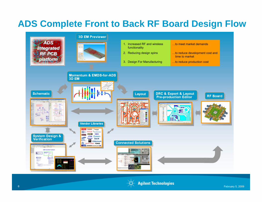
ADS Complete Front to Back RF Board Design Flow
ADS Integrated RF PCB platform
ADS Integrated RF PCB platform
1. Increased RF and wireless functionality
2. Reducing design spins
3. Design For Manufacturing
…to meet market demands
…to reduce development cost and time to market
…to reduce production cost
February 5, 20097
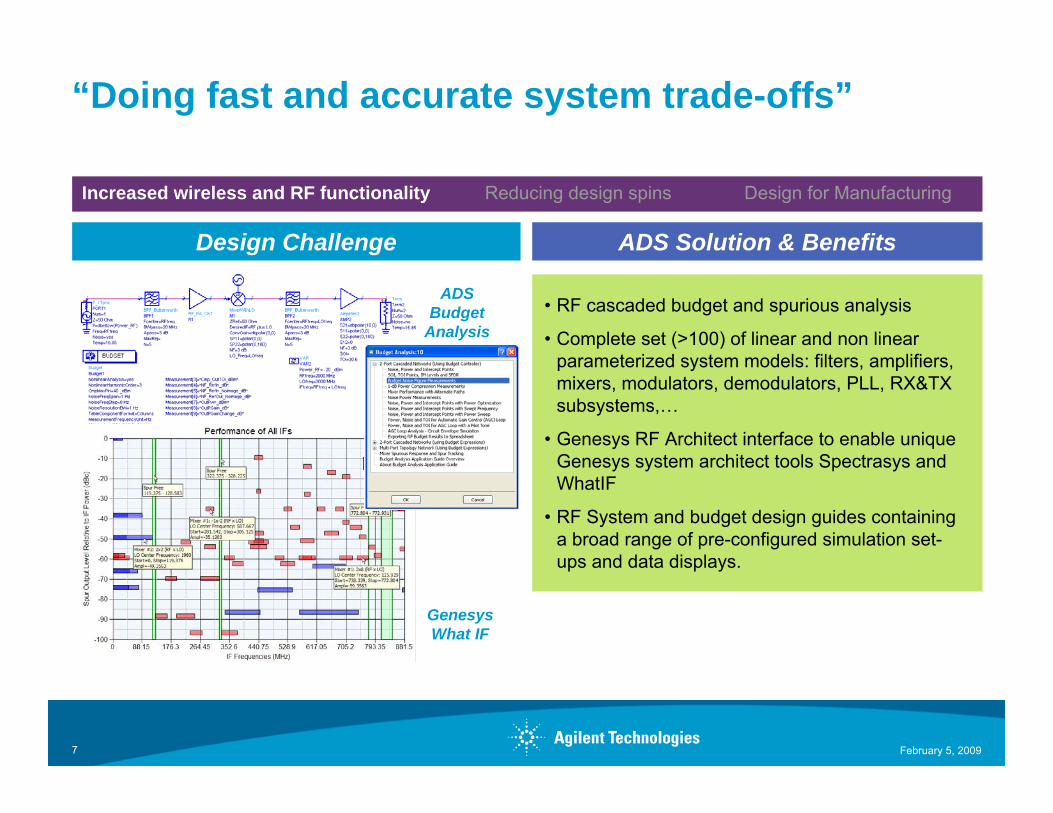
• RF cascaded budget and spurious analysis
• Complete set (>100) of linear and non linear parameterized system models: filters, amplifiers, mixers, modulators, demodulators, PLL, RX&TX subsystems,…
• Genesys RF Architect interface to enable unique Genesys system architect tools Spectrasys and WhatIF
• RF System and budget design guides containing a broad range of pre-configured simulation set-ups and data displays.
ADS Budget
Analysis
GenesysWhat IF
Design Challenge ADS Solution & Benefits
“Doing fast and accurate system trade-offs”
Increased wireless and RF functionality Reducing design spins Design for Manufacturing
February 5, 20098
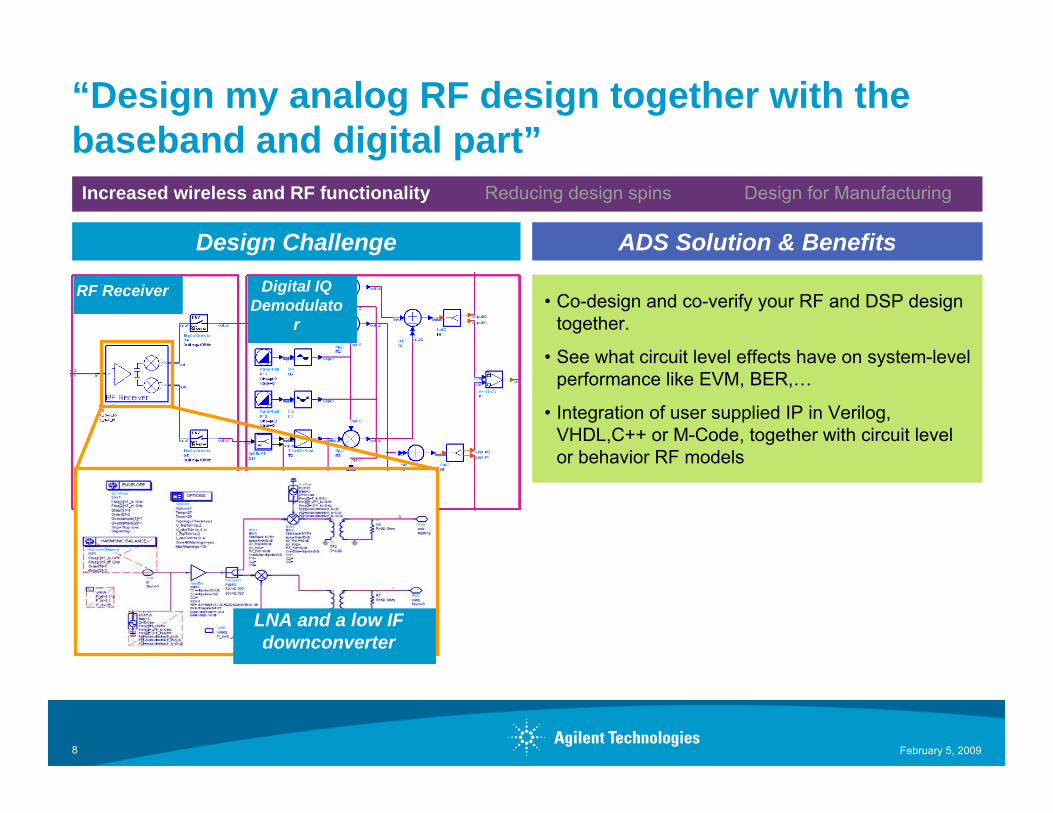
• Co-design and co-verify your RF and DSP design together.
• See what circuit level effects have on system-level performance like EVM, BER,…
• Integration of user supplied IP in Verilog, VHDL,C++ or M-Code, together with circuit level or behavior RF models
LNA and a low IF downconverter
RF Receiver Digital IQ Demodulato
r
“Design my analog RF design together with the baseband and digital part”Increased wireless and RF functionality Reducing design spins Design for Manufacturing
Design Challenge ADS Solution & Benefits
February 5, 20099
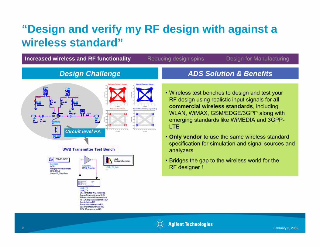
Circuit level PA
• Wireless test benches to design and test your RF design using realistic input signals for all commercial wireless standards, including WLAN, WiMAX, GSM/EDGE/3GPP along with emerging standards like WiMEDIA and 3GPP-LTE
• Only vendor to use the same wireless standard specification for simulation and signal sources and analyzers
• Bridges the gap to the wireless world for the RF designer !
“Design and verify my RF design with against a wireless standard”Increased wireless and RF functionality Reducing design spins Design for Manufacturing
Design Challenge ADS Solution & Benefits
February 5, 200910
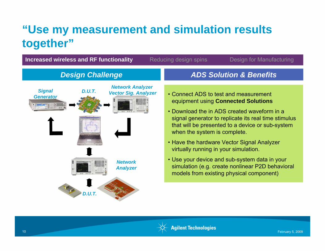
Network AnalyzerSignal
GeneratorD.U.T.
Network Analyzer
D.U.T.
Vector Sig. Analyzer • Connect ADS to test and measurement equipment using Connected Solutions
• Download the in ADS created waveform in a signal generator to replicate its real time stimulus that will be presented to a device or sub-system when the system is complete.
• Have the hardware Vector Signal Analyzer virtually running in your simulation.
• Use your device and sub-system data in your simulation (e.g. create nonlinear P2D behavioral models from existing physical component)
“Use my measurement and simulation results together”Increased wireless and RF functionality Reducing design spins Design for Manufacturing
Design Challenge ADS Solution & Benefits
February 5, 200911
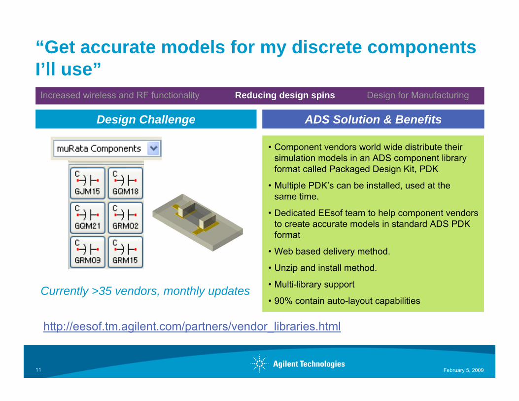
http://eesof.tm.agilent.com/partners/vendor_libraries.html
Currently >35 vendors, monthly updates
• Component vendors world wide distribute their simulation models in an ADS component library format called Packaged Design Kit, PDK
• Multiple PDK’s can be installed, used at the same time.
• Dedicated EEsof team to help component vendors to create accurate models in standard ADS PDK format
• Web based delivery method.
• Unzip and install method.
• Multi-library support
• 90% contain auto-layout capabilities
“Get accurate models for my discrete components I’ll use”Increased wireless and RF functionality Reducing design spins Design for Manufacturing
Design Challenge ADS Solution & Benefits
February 5, 200912
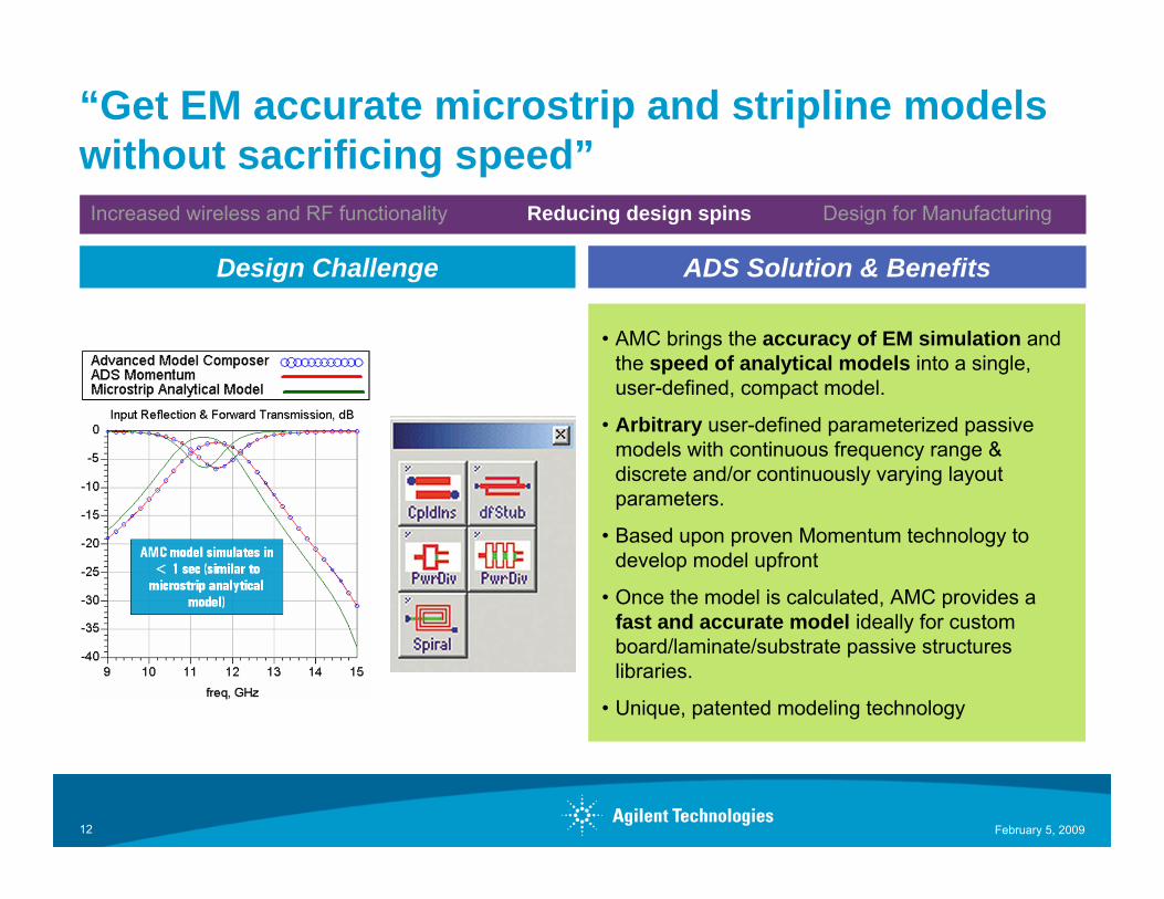
• AMC brings the accuracy of EM simulation and the speed of analytical models into a single, user-defined, compact model.
• Arbitrary user-defined parameterized passive models with continuous frequency range & discrete and/or continuously varying layout parameters.
• Based upon proven Momentum technology to develop model upfront
• Once the model is calculated, AMC provides a fast and accurate model ideally for custom board/laminate/substrate passive structures libraries.
• Unique, patented modeling technology
“Get EM accurate microstrip and stripline models without sacrificing speed”Increased wireless and RF functionality Reducing design spins Design for Manufacturing
Design Challenge ADS Solution & Benefits
February 5, 200913
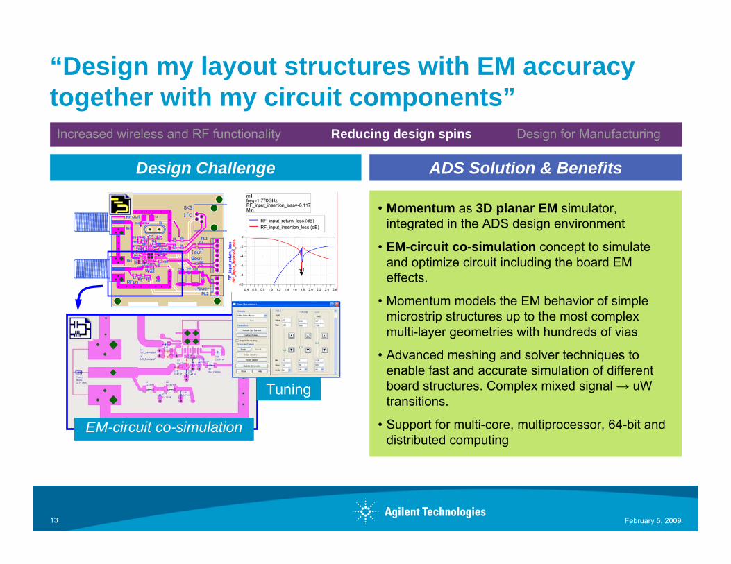
• Momentum as 3D planar EM simulator, integrated in the ADS design environment
• EM-circuit co-simulation concept to simulate and optimize circuit including the board EM effects.
• Momentum models the EM behavior of simple microstrip structures up to the most complex multi-layer geometries with hundreds of vias
• Advanced meshing and solver techniques to enable fast and accurate simulation of different board structures. Complex mixed signal → uWtransitions.
• Support for multi-core, multiprocessor, 64-bit and distributed computing
EM-circuit co-simulation
Tuning
“Design my layout structures with EM accuracy together with my circuit components”Increased wireless and RF functionality Reducing design spins Design for Manufacturing
Design Challenge ADS Solution & Benefits
February 5, 200914
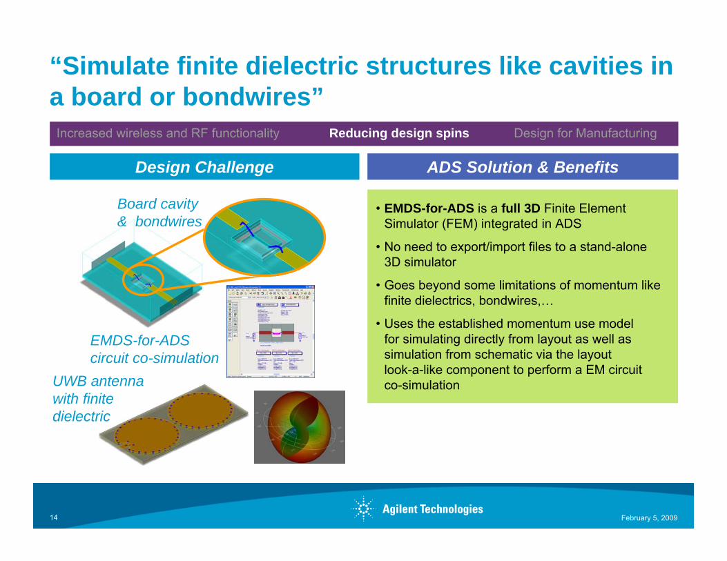
Board cavity & bondwires
UWB antenna with finite dielectric
EMDS-for-ADS circuit co-simulation
• EMDS-for-ADS is a full 3D Finite Element Simulator (FEM) integrated in ADS
• No need to export/import files to a stand-alone 3D simulator
• Goes beyond some limitations of momentum like finite dielectrics, bondwires,…
• Uses the established momentum use model for simulating directly from layout as well as simulation from schematic via the layout look-a-like component to perform a EM circuit co-simulation
“Simulate finite dielectric structures like cavities in a board or bondwires”Increased wireless and RF functionality Reducing design spins Design for Manufacturing
Design Challenge ADS Solution & Benefits
February 5, 200915
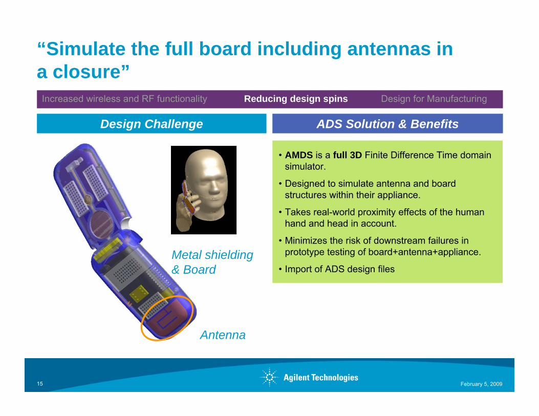
Antenna
Metal shielding & Board
• AMDS is a full 3D Finite Difference Time domain simulator.
• Designed to simulate antenna and board structures within their appliance.
• Takes real-world proximity effects of the human hand and head in account.
• Minimizes the risk of downstream failures in prototype testing of board+antenna+appliance.
• Import of ADS design files
“Simulate the full board including antennas in a closure”Increased wireless and RF functionality Reducing design spins Design for Manufacturing
Design Challenge ADS Solution & Benefits
February 5, 200916
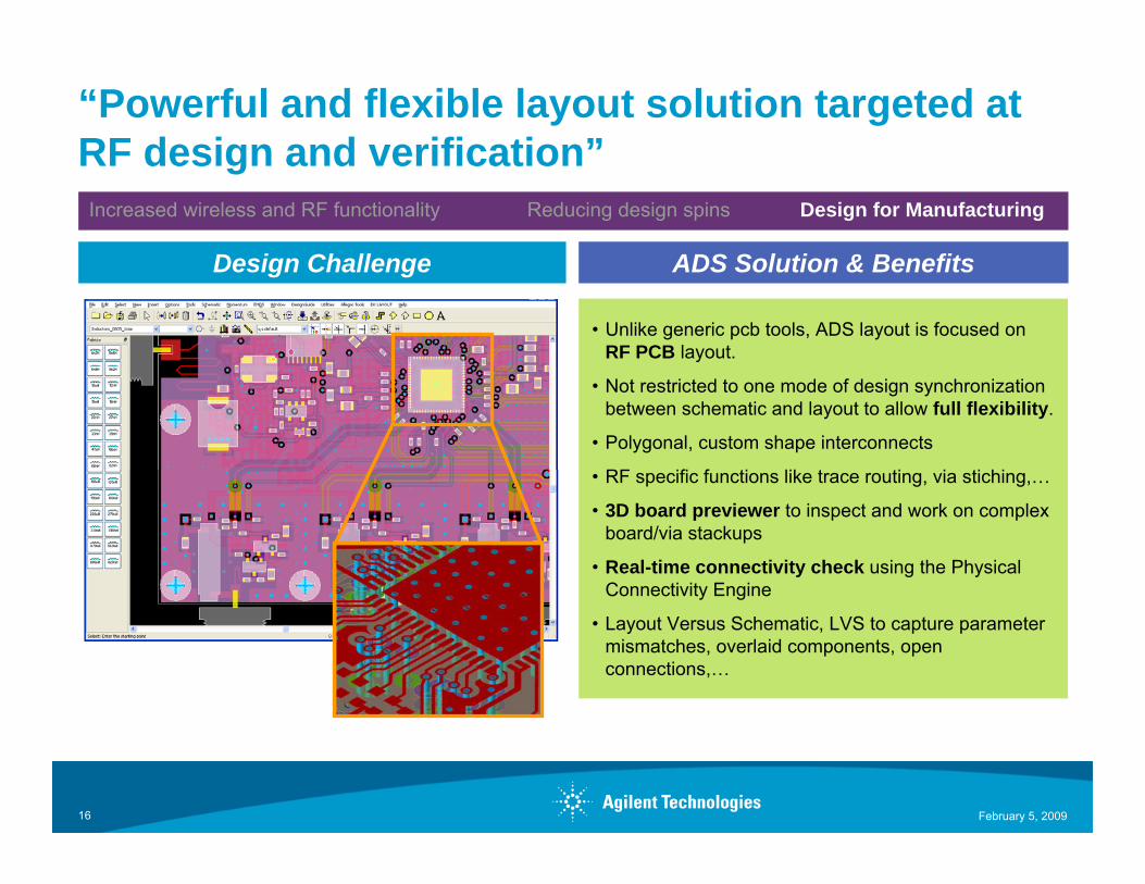
• Unlike generic pcb tools, ADS layout is focused on RF PCB layout.
• Not restricted to one mode of design synchronization between schematic and layout to allow full flexibility.
• Polygonal, custom shape interconnects
• RF specific functions like trace routing, via stiching,…
• 3D board previewer to inspect and work on complex board/via stackups
• Real-time connectivity check using the Physical Connectivity Engine
• Layout Versus Schematic, LVS to capture parameter mismatches, overlaid components, open connections,…
“Powerful and flexible layout solution targeted at RF design and verification”Increased wireless and RF functionality Reducing design spins Design for Manufacturing
Design Challenge ADS Solution & Benefits
February 5, 200917
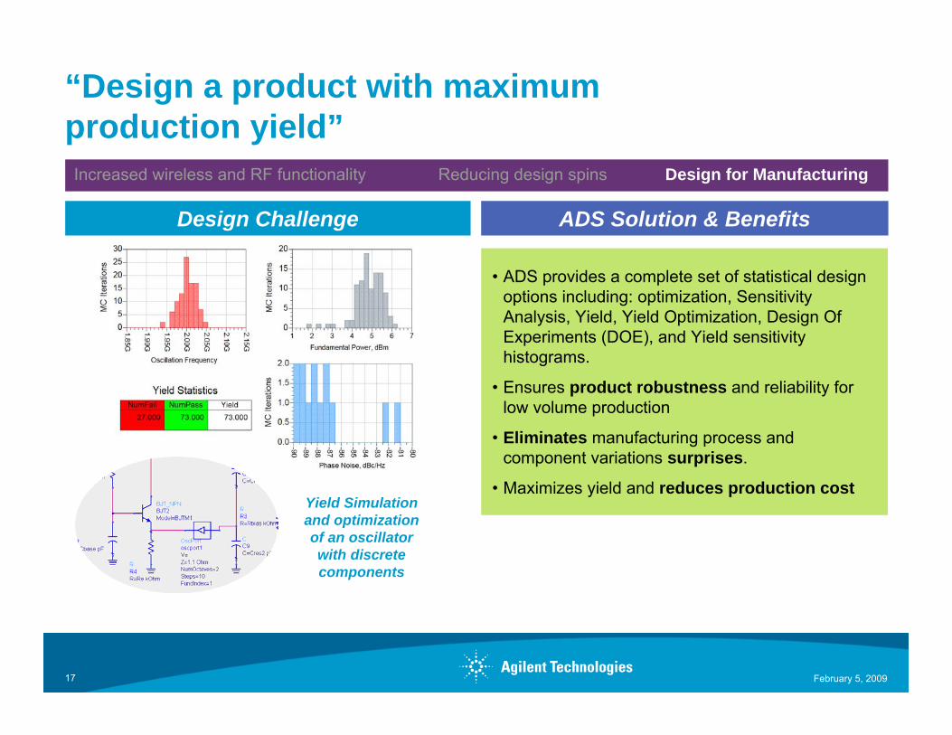
Yield Simulation and optimization of an oscillator with discrete components
• ADS provides a complete set of statistical design options including: optimization, Sensitivity Analysis, Yield, Yield Optimization, Design Of Experiments (DOE), and Yield sensitivity histograms.
• Ensures product robustness and reliability for low volume production
• Eliminates manufacturing process and component variations surprises.
• Maximizes yield and reduces production cost
“Design a product with maximum production yield”Increased wireless and RF functionality Reducing design spins Design for Manufacturing
Design Challenge ADS Solution & Benefits
February 5, 200918
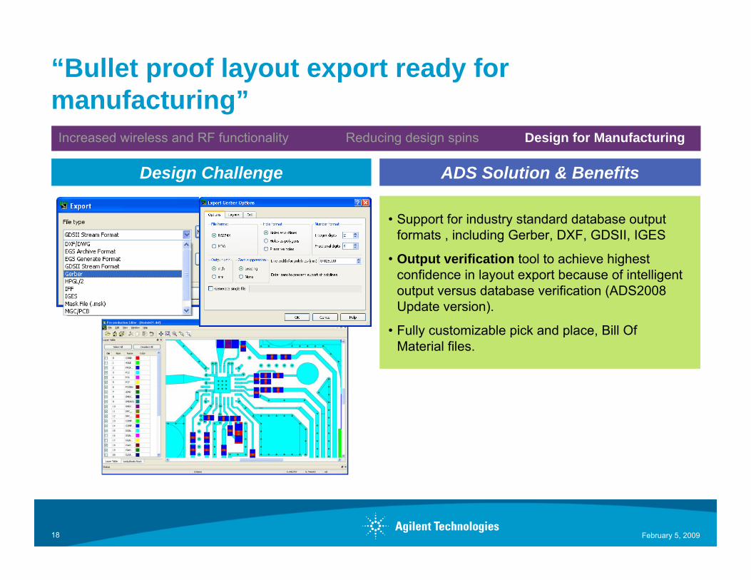
• Support for industry standard database output formats , including Gerber, DXF, GDSII, IGES
• Output verification tool to achieve highest confidence in layout export because of intelligent output versus database verification (ADS2008 Update version).
• Fully customizable pick and place, Bill Of Material files.
“Bullet proof layout export ready for manufacturing”Increased wireless and RF functionality Reducing design spins Design for Manufacturing
Design Challenge ADS Solution & Benefits
February 5, 200919
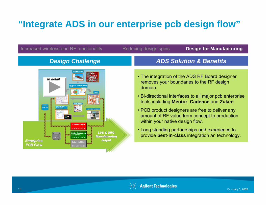
In detail• The integration of the ADS RF Board designer
removes your boundaries to the RF design domain.
• Bi-directional interfaces to all major pcb enterprise tools including Mentor, Cadence and Zuken
• PCB product designers are free to deliver any amount of RF value from concept to production within your native design flow.
• Long standing partnerships and experience to provide best-in-class integration an technology.
“Integrate ADS in our enterprise pcb design flow”
Increased wireless and RF functionality Reducing design spins Design for Manufacturing
Design Challenge ADS Solution & Benefits
February 5, 200920
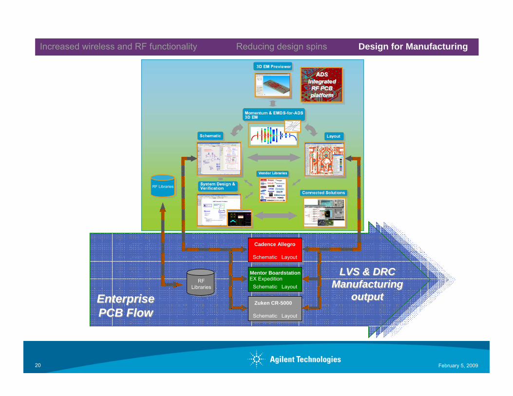
Enterprise PCB Flow
LVS & DRC Manufacturing
outputEnterprise PCB FlowEnterprise PCB Flow
RF Libraries
RF Libraries
LVS & DRC Manufacturing
output
LVS & DRC Manufacturing
output
Cadence Allegro
Schematic Layout
Mentor Boardstation
Schematic Layout
Zuken CR-5000
Schematic Layout
EX Expedition
Increased wireless and RF functionality Reducing design spins Design for Manufacturing
February 5, 200921
www.agilent.com
For more information about Agilent EEsof EDA, visit:www.agilent.com/find/eesof
www.agilent.com
For more information on Agilent Technologies’ products, applications or services, please contact your local Agilent office. The complete list is available at:
www.agilent.com/find/contactus
Contact Agilent at:
AmericasCanada (877) 894-4414Latin America 305 269 7500United States (800) 829-4444
Asia PacificAustralia 1 800 629 485China 800 810 0189Hong Kong 800 938 693India 1 800 112 929Japan 0120 (421) 345Korea 080 769 0800Malaysia 1 800 888 848Singapore 1 800 375 8100Taiwan 0800 047 866Thailand 1 800 226 008
Europe & Middle EastAustria 01 36027 71571Belgium 32 (0) 2 404 93 40Denmark 45 70 13 1515Finland 358 (0) 10 855 2100France 0825 010 700**0.125 /minuteGermany 07031 464 6333Ireland 1890 924 204Israel 972-3-9288-504/544Italy 39 02 92 60 8484Netherlands 31 (0) 20 547 2111Spain 34 (91) 631 3300Sweden 0200-88 22 55Switzerland 0800 80 53 53United Kingdom 44 (0) 118 9276201Other European Countries:www.agilent.com/find/contactus
Product specifications and descriptions in this document subject to change without notice.
© Agilent Technologies, Inc. 2009Published in the U.S.A. February 5, 20095990-3559EN