ads1675ref user's guide - produktinfo.conrad.com · 9 xem3010 driver installation (screen 4)...
TRANSCRIPT

User's GuideSBAU162A–December 2009–Revised September 2010
ADS1675REF
ADS1675REF
This user's guide describes the characteristics, operation, and use of the ADS1675REF reference designboard. This reference design board (REF) is an evaluation platform for the ADS1675, a 4MSPS,high-speed, high-precision, 24-bit analog-to-digital converter (ADC). The ADS1675REF allows evaluationof all aspects of the ADS1675 device. A complete circuit description as well as schematic diagram and billof materials are included.
The following related documents are available through the Texas Instruments web site athttp://www.ti.com except where indicated.
Related Documents
Device Literature Number
ADS1675 SBAS416C
THS4503 SLOS352D
OPA211 SBOS377
REF5025 SBOS410
XEM3010 http://www.opalkelly.com/products/xem3010
ADCPro is a trademark of Texas Instruments.Microsoft, Windows, WindowsXP, Vista are registered trademarks of Microsoft Corporation.All other trademarks are the property of their respective owners.
1SBAU162A–December 2009–Revised September 2010 ADS1675REFSubmit Documentation Feedback
Copyright © 2009–2010, Texas Instruments Incorporated
Preface www.ti.com
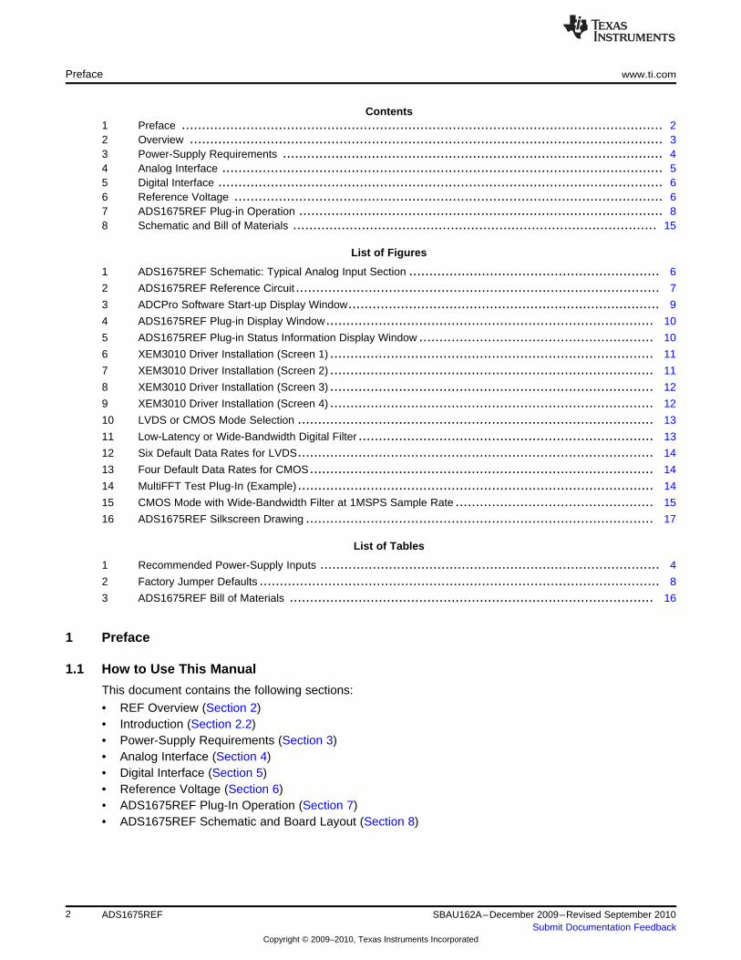
Contents1 Preface ....................................................................................................................... 22 Overview ..................................................................................................................... 33 Power-Supply Requirements .............................................................................................. 44 Analog Interface ............................................................................................................. 55 Digital Interface .............................................................................................................. 66 Reference Voltage .......................................................................................................... 67 ADS1675REF Plug-in Operation .......................................................................................... 88 Schematic and Bill of Materials .......................................................................................... 15
List of Figures
1 ADS1675REF Schematic: Typical Analog Input Section .............................................................. 6
2 ADS1675REF Reference Circuit .......................................................................................... 7
3 ADCPro Software Start-up Display Window............................................................................. 9
4 ADS1675REF Plug-in Display Window................................................................................. 10
5 ADS1675REF Plug-in Status Information Display Window .......................................................... 10
6 XEM3010 Driver Installation (Screen 1) ................................................................................ 11
7 XEM3010 Driver Installation (Screen 2) ................................................................................ 11
8 XEM3010 Driver Installation (Screen 3) ................................................................................ 12
9 XEM3010 Driver Installation (Screen 4) ................................................................................ 12
10 LVDS or CMOS Mode Selection ........................................................................................ 13
11 Low-Latency or Wide-Bandwidth Digital Filter ......................................................................... 13
12 Six Default Data Rates for LVDS........................................................................................ 14
13 Four Default Data Rates for CMOS..................................................................................... 14
14 MultiFFT Test Plug-In (Example)........................................................................................ 14
15 CMOS Mode with Wide-Bandwidth Filter at 1MSPS Sample Rate ................................................. 15
16 ADS1675REF Silkscreen Drawing ...................................................................................... 17
List of Tables
1 Recommended Power-Supply Inputs .................................................................................... 4
2 Factory Jumper Defaults ................................................................................................... 8
3 ADS1675REF Bill of Materials .......................................................................................... 16
1 Preface
1.1 How to Use This Manual
This document contains the following sections:
• REF Overview (Section 2)• Introduction (Section 2.2)• Power-Supply Requirements (Section 3)• Analog Interface (Section 4)• Digital Interface (Section 5)• Reference Voltage (Section 6)• ADS1675REF Plug-In Operation (Section 7)• ADS1675REF Schematic and Board Layout (Section 8)
2 ADS1675REF SBAU162A–December 2009–Revised September 2010Submit Documentation Feedback
Copyright © 2009–2010, Texas Instruments Incorporated

www.ti.com Overview
2 Overview
2.1 Features
ADS1675REF Features:• Full-featured evaluation board for the ADS1675 24-bit, Delta-Sigma (ΔΣ) analog-to-digital converter• Analog inputs can be applied to the ADC through an analog input driver circuit• Onboard voltage references• Clock options: onboard adjustable frequency default setup is 32MHz• Supports both serial CMOS and low-voltage differential signaling (LVDS) interface modes by two
different versions of software plug-in
ADCPro™ Plug-In Features:• Easy-to-use evaluation software for Microsoft® Windows® XP• Data collection to text files• Built-in analysis tools including scope, FFT, and histogram displays• Complete control of board settings• Easily expandable with new analysis plug-in tools from Texas Instruments
This kit combines the ADS1675REF board with the FPGA and SDRAM-based XEM3010 board, andincludes ADCPro™ software for evaluation.
You can connect the ADS1675REF to the XEM3010 board and then to a computer via an available USBport. This manual shows how to use the XEM3010 as part of the ADS1675REF kit, but does not providetechnical details about the XEM3010 itself. Refer to the Opal Kelly website (at www.opalkelly.com) forspecific details about the XEM3010-1500.
ADCPro is a program for collecting, recording, and analyzing data from ADC evaluation boards. ADCProhas a number of plug-in programs, so it can be expanded easily with new test and data collection plug-ins.You control the ADS1675REF with a plug-in that runs in ADCPro. For more information about ADCPro,see the ADCPro™ Analog-to-Digital Converter Evaluation Software User's Guide (literature numberSBAU128), available for download from the TI web site.
This manual covers the operation of both the ADS1675REF and the ADS1675REF Plug-in for ADCPro.Throughout this document, the abbreviation REF and the term reference board are synonymous with theADS1675REF.
2.2 Introduction
The ADS1675REF is a 24-bit, ΔΣ analog-to-digital converter that operates from independent AVDD (+5V)and DVDD (+3V) supplies. The analog input pre-amplifier THS4503 can be powered from +9V and -4Vsupplies. The XEM3010 FPGA processor board can be supplied either with a +5V external wall adapterpower supply or with +5V (JP4) from the ADS1675REF board itself.
The maximum sample rate of the ADS1675 is 4MSPS. The maximum output clock speed is 96MHz.
The output interface can be configured as either CMOS or LVDS interface; the ADS1675REF works easilywith both interfaces.
There are two digital decimation filters built into the ADS1675 device. The first one is low-latency filter thatcan reduce digital processing time, but only provide narrow signal bandwidth; this filter is best used for fastdigital processing applications. The second option is a wide-bandwidth digital filter that can provide amuch wider and flat signal bandwidth, but with slower processing time.
The ADS1675REF hardware platform consists of a two-board solution: one ADS1675REF printed circuitboard (PCB) plus one FPGA processor board (XEM3010). The ADS1675REF hardware uses a verycommon FPGA Spartan-3, Micron 16-MByte (16-bit word-wide) synchronous DRAM (SDRAM) chip,Cypress CY22393 PLL, and USB 2.0 microcontroller.
3SBAU162A–December 2009–Revised September 2010 ADS1675REFSubmit Documentation Feedback
Copyright © 2009–2010, Texas Instruments Incorporated

Power-Supply Requirements www.ti.com
The SDRAM controller code is preloaded within the FPGA. The ADCPro software works with the USB 2.0driver in the ADS1675REF environment, so that 8M, 24-bit sampled ADC data can be captured and savedin the SDRAM per single acquisition in order to allow the FPGA processor to do post-data processing ortransfer the test data continually through the FPGA, SDRAM, and USB interface into a PC processor forfurther data processing.
The Cypress CY22393 PLL can provide up to five clocks. The ADS1675REF platform uses one 48MHzclock for the USB microcontroller, one 64MHz clock for the SDRAM chip, one 64MHz clock for the FPGAprocessor, and one 32MHz clock for the ADS1675 device.
The ADS1675REF supports fast response mode for both the wide-bandwidth and low-latency filter paths,as well as an internal shift clock (SCLK) mode for LVDS and CMOS digital output interfaces.
3 Power-Supply Requirements
WARNINGThe Opal Kelly XEM3010 board can only accept a maximum 5Vpower supply. When the 5V external wall adaptor is applied,remove JP4. (See Table 1 for additional details.)
The factory configuration of the board is for the analog input driver THS4503 with +9V and –4V suppliesand a shared +5V supply for analog and digital REF board circuitry sections as well as the XEM3010board. For the best total harmonic distortion (THD) performance, the user can provide independent digital+5V to +5VD, +3.0V to 3.3VD, and wall adaptor +5V to P1 on the XEM3010 board. All power to the boardis recommend to be sourced from a well-regulated linear supply that has current-limiting capabilities; forexample, a 40mA limit for +9V and –4V, and 400mA limit for +VA.
Power must be supplied through jumpers J2, J4, J5, and J9 (top side of the REF board) and port P1 onthe XEM3010 board. Table 1 shows the recommended power-supply input configuration.
Table 1. Recommended Power-Supply Inputs
Signal Name Connector Number Description
+5VA J5-1 J5-2 Analog +5V supply
+VCC J4-1 J4-2 Analog input driver +9V supply
–VCC J4-3 J4-2 Analog input driver –4V supply
+5VD (optional for the bestperformance; remove R39 when using J9-1 J9-2 Digital +5V supply+5VD)
+3.3VD (optional for the bestperformance; remove JP2 when J2-1 J2-2 Digital +3.0V supplyapplying +3.0V)
+5V (optional for the best performance;remove JP4 when applying a +5V wall P1-1 P1-2 XEM3010 board +5V wall adaptor supplyadaptor to the XEM3010)
For standalone operation, the power sources can be applied via various test points located on the REFboard. Refer to the schematic (located at the end of this document) for additional details.
3.1 Analog Input Driver +9V and –4V Supplies
The ADS1675REF analog input driver is a THS4503 (U3), a wideband, fully-differential amplifier, to drivethe differential inputs of the ADS1675 (U4) . This device was selected because of its wide bandwidth(370MHz) and low harmonic distortion. It is pre-configured at the factory for +9V and –4V analogoperation. The THS4503 can tolerate maximum power supplies of ±7.5VDC. Care must be taken to ensurethe user-supplied 15VDC limit is not exceeded, or potential damage to the op amps under the test circuitscan occur. The +9V and –4V voltages are to be applied to J4 pins +VCC and –VCC referenced to GND.
4 ADS1675REF SBAU162A–December 2009–Revised September 2010Submit Documentation Feedback
Copyright © 2009–2010, Texas Instruments Incorporated

www.ti.com Analog Interface
3.2 Analog +5V Supply
The ADS1675REF board requires an independent analog +5V supply to power the analog portion of thedevice under test, the external reference, and the external reference buffer, as well as provide theamplifier common-mode voltage. This voltage is applied to J5 pin 3 and is denoted as +5VA. This supplycan be monitored at TP7.
3.3 Digital +5V Supply
For the best THD performance, the ADS1675 requires an independent digital +5V supply to power theclock portion of the device under test. This voltage is applied to J9 pin 3 and is denoted as +5VD. Thissupply can be monitored at TP3. For a quick function test, the digital +5VD can be shared with the analog+5VA on this REF board. R39 is a short circuit that supplies both the analog and digital 5V to the ADS1675device.
3.4 Digital +3.0V Supply
For the best THD performance, the ADS1675 also requires an independent digital +3.0V supply to powerthe digital portion of the device under test. This voltage is applied to J2 pin 3 and is denoted as +3.3VD.This supply can be monitored at TP5. For a quick function test, the digital +3.0V can be fed back from the3.3V regulator on the XEM3010 board and connected by jumper JP2 on the REF.
For optimal performance, it is recommended to remove the shunt jumpers from JP2 and JP4. Thisconfiguration requires the user to supply an independent 3.0V digital supply to the ADS1675 at J2. Theuser must also provide separate power to the XEM3010 at P1; refer to the Opal Kelly website for specificdetails about configuring the XEM3010 board.
3.5 XEM3010 Board +5V Supply
To obtain the best THD performance, the ADS1675 requires an independent +5V supply to power theXEM3010 board. This voltage is applied to P1 on the XEM3010 from an external wall adapter powersupply. For a quick function test, the +5V can be shared with the digital +5VD on the ADS1675REF byjumper JP4.
4 Analog Interface
The analog circuit of the board is divided into four parts. The first part is the analog input buffer orfront-end circuit of the ADC. Its function is to provide optional gain and impedance matching of the inputsignal. The second part of the analog circuit is the analog power supplies for both the high voltage rails onthe ADC and the input buffer. The final sections of the analog input include the basic analog functions ofthe ADS1675 and the optional external reference circuit. Each of these sections is described below.
The analog inputs to the ADS1675REF board can be applied to J1 and J3 of the input differentialconnectors. The range of the analog input depends on the range setting of the ADS1675 and THS4503.
The analog input to the ADS1675REF board consists of the THS4503 operational amplifier. The THS4503is powered from a user-provided, 9V and –4V analog supply. The amplifier is used as true differentialdriver. When the analog supply is 5V, the ADS1675 analog difference input common-mode voltage is2.5V. This configuration requires the output of the THS4503 amplifier common-mode voltage to be set as2.5V. The common-mode voltage to the THS4503 is set by the onboard REF5025 (U1), which sets thisvoltage at 2.5V.
5SBAU162A–December 2009–Revised September 2010 ADS1675REFSubmit Documentation Feedback
Copyright © 2009–2010, Texas Instruments Incorporated

R18
0W
R15
249W
R20
10W
R13
249W
R19
10W
R17
0W
C17
750pF
AINP
AINNVIN+
VIN-
COM
VOUT-
VOUT+
8
2
1 4
5P
D
VS
+V
S-
VS-
VS-
THS4503ID
C40
10 Fm
C39
0.1 Fm
-VCC
C38
10 Fm
C37
0.1 Fm
+VCC
RCM
JP1
6
C14
Not Installed
C72
C12
37
Not Installed
Not Installed
Digital Interface www.ti.com
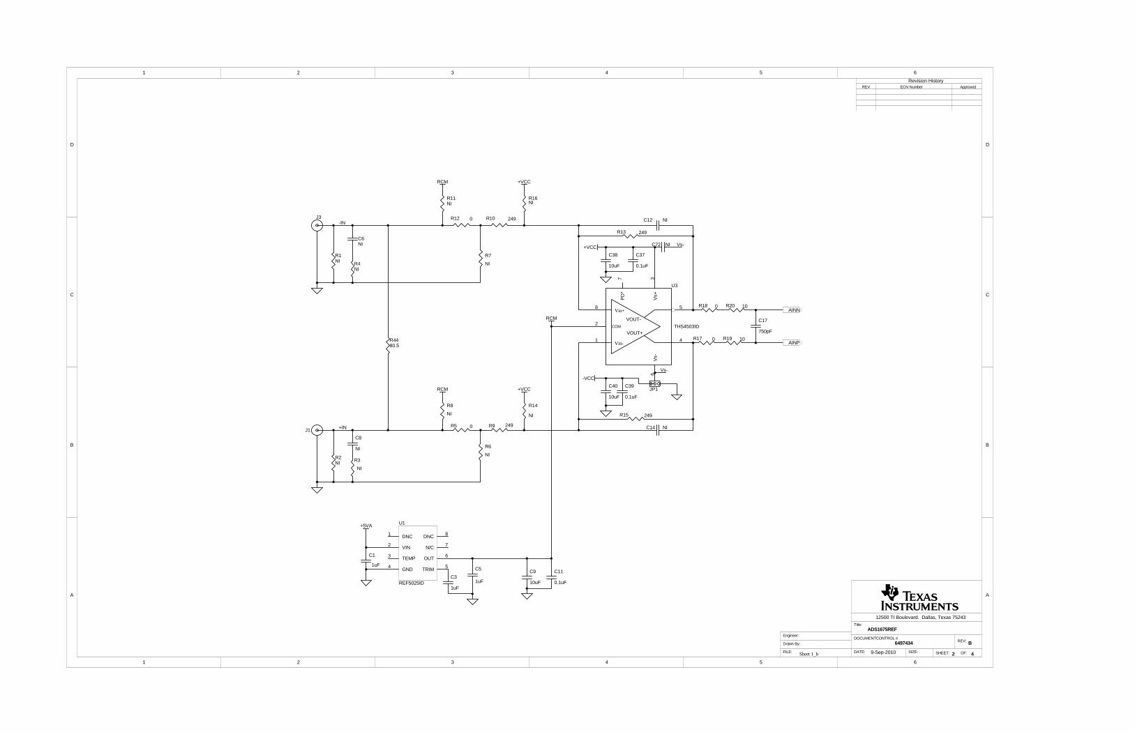
To maximize the dynamic range of the THS4503 and reduce the THD impact from this amplifier, +9V and–4V are used for this THS4503. This configuration gives a maximum ±6.5V swing range. Figure 1illustrates the typical analog input section of the ADS1675REF.
Figure 1. ADS1675REF Schematic: Typical Analog Input Section
5 Digital Interface
The ADS1675REF is designed for easy interfacing with the USB2.0 interface for use with the XEM3010board. The ADS1675REF kit also provides ADCPro software so that the user can configure the ADS1675and read out the captured data through the USB interface on the XEM3010 board.
6 Reference Voltage
The ADS1675REF provides a 3.0V reference source via a REF5030 (U2) and OPA211A (U5) to provide ahigh-quality reference voltage for ADS1675. The REF5030 (U2) generates the 3.0V reference signal. Theoutput of the REF5030 is heavily filtered to remove noise. The onboard OPA211 (U5) again filters andbuffers the reference signal so that the reference signal noise to the ADS1675 is less than the noisegenerated by the converter itself. The OPA211 is a low-noise, unity-gain stable amplifier that provides areliable current source for the ADS1675 reference input. The OPA211 and output decoupling capacitorswork together to settle the VREFP (ADS1675) reference input voltage to within ±1/2 LSB, every 50ns. Thisboard uses a 10mF ceramic capacitor with a 0.1mF ceramic capacitor directly across the reference inputs,VREFP and VREFN. Note that the 10mF and 0.1mF capacitors are placed as close to the ADS1675reference pins as possible. These capacitors further reduce noise that is common to both inputs. TheADS1675 VREFN pin goes to ground.
6 ADS1675REF SBAU162A–December 2009–Revised September 2010Submit Documentation Feedback
Copyright © 2009–2010, Texas Instruments Incorporated

DNCDNC
VIN
TEMP
GND
N/C
OUT
TRIM
REF5030AID
1
1
2
2
3
3
4
4
5
5
6
6
7
7
8
8
+5VA
+5VA
C10
1 Fm
C15
1 Fm
C21
1 Fm
C47
10 Fm
C46
10 FmC48
1 Fm
C20
10 Fm
C19
0.1 Fm
R21
1kW
R22
49.9W
R25
100W
OPA211AIDGK
C22
0.15 Fm
C30
0.1 Fm
www.ti.com Reference Voltage
Figure 2 shows the ADS1675REF reference circuit.
Figure 2. ADS1675REF Reference Circuit
7SBAU162A–December 2009–Revised September 2010 ADS1675REFSubmit Documentation Feedback
Copyright © 2009–2010, Texas Instruments Incorporated

ADS1675REF Plug-in Operation www.ti.com
7 ADS1675REF Plug-in Operation
This section provides information on using the ADS1675REF Plug-in, including setup, program installation,and program usage. The board is factory-configured for the analog input driver THS4503 with +9V and–4V supplies and the shared analog, digital, and XEM3010 board with a +5VA supply on the ADS1675.Table 2 lists the default jumper setup.
Table 2. Factory Jumper Defaults
Shunt Jumpers Position Description
ADS1675REF Jumpers
U3 Negative Supply (JP1) 1-2; use 2mm shunt jumper -V is supplied by J4
OK3.3V (JP2) Closed; use 2mm shunt jumper 3.3VDC is supplied to ADS1675REFfrom the Opal Kelly Board
OK5V (JP4) Closed; use 2mm shunt jumper 5.0VDC is supplied to the Opal Kellyboard from the user's external 5Vsupply
CAPT (JP3) Open Strobe for data capture card used indebug
XEM3010 Jumpers
J1 Closed
J2 Open
JP1 Open
To prepare to evaluate the ADS1675 with the ADS1675REF Plug-in, complete the following steps:
Step 1. Verify all jumper settings against the settings described in Table 2.Step 2. Download the latestversion of the ADCPro software from www.ti.com/adcpro.Step 3. Install the ADCPro application. Once the application is installed, run the
ADS1675REF-plug-in file located on the CD-ROM (included with the ADS1675REF package)under the Plug-in Installer directory. Please note that while installing the ADS1675 plug-in, aseparate installer for the Opal Kelly board will also be launched. Accept all default settingsand choose the Continue anyway option if you see a warning regarding driver authenticity.
Step 4. Complete the Microsoft Windows USB driver installation process.Step 5. Ensure the XEM3010 board is firmly seated onto the mating connectors found on the
ADS1675REF board.Step 6. Apply power to the ADS1675REF board as described in Section 7.2; note that best
performance is achieved by using clean linear supplies. Set the current limits and voltagesfirst, then connect power leads to the board before enabling the supply outputs.
Step 7. Apply +9V and –4V to the screw terminals marked J4. +VCC, GND, and –VCC are labeledbelow the entry point to the screw terminal.
Step 8. Apply +5 VDC to the screw terminal marked J5. +5VA and GND are marked at the terminalentry points. R39 is a short circuit that supplies both the digital 5V to the ADS1675 and 5V tothe XEM3010 board. The XEM3010 generates a 3.3V supply that is fed back to theADS1675.
7.1 Installing the ADCPro Software
The latest version of the ADCPro software is available from Texas Instruments' website athttp://www.ti.com/adcpro. The CD-ROM shipped with the ADS1675REF may not contain the latestsoftware, but the ADCPro installer will check for updates when executed (if connected to the Internet), andthen give you the option of downloading and installing the latest version. Refer to the ADCPro™Analog-to-Digital Converter Evaluation Software User's Guide for instructions on installing and usingADCPro.
To install the ADS1675REF plug-in, run the file: ads1675ref-plug-in-1.0.0.exe (1.0.0 is the versionnumber, and increments with software version releases; you may have a different version on your CD).Double-click the file to run it; then follow the instructions shown. After installation, you can use the ADCProUpdate Check feature to check for newer versions of the ADS1675REF plug-in.
8 ADS1675REF SBAU162A–December 2009–Revised September 2010Submit Documentation Feedback
Copyright © 2009–2010, Texas Instruments Incorporated

www.ti.com ADS1675REF Plug-in Operation
The software should now be installed, but the USB drivers may not have been loaded by the PC operatingsystem. The USB driver upload step completes when the ADCPro software is executed (see Section 7.2,Running the Software and Completing the Driver Installation).
7.2 Running the Software and Completing the Driver Installation
NOTE: The software is continually under development. These instructions and screen images arecurrent at the time of this writing, but may not exactly correspond to future releases.
ADCPro uses a series of software plug-ins to communicate with the ADS1675REF. The ADS1675REFplug-in is included in the ADS1675REF package.
The program currently runs only on Microsoft Windows platforms of WindowsXP®; Windows Vista® is notsupported.
Follow these procedures to run ADCPro and complete the necessary driver installation.
Step 1. Start the software by selecting ADCPro from the Windows Start menu. The screen in Figure 3appears.
Figure 3. ADCPro Software Start-up Display Window
9SBAU162A–December 2009–Revised September 2010 ADS1675REFSubmit Documentation Feedback
Copyright © 2009–2010, Texas Instruments Incorporated

ADS1675REF Plug-in Operation www.ti.com
spaceStep 2. Select ADS1675REF from the REF drop-down menu. The ADS1675REF plug-in appears in
the left pane, as shown in Figure 4.
Figure 4. ADS1675REF Plug-in Display Window
Step 3. The ADS1675REF plug-in window has a status area at the top of the screen. When theplug-in is first loaded, the plug-in searches for the board. You will see a series of messagesin the status area that indicate this action, such as Connected (as Figure 5 illustrates).
Figure 5. ADS1675REF Plug-in Status Information Display Window
Step 4. Apply power to the REF board and connect the board to an available PC USB port.Step 5. If you have not yet loaded the XEM3010 system drivers, Windows will display the Windows
Found New Hardware Wizard sequence (illustrated in Figure 6 through Figure 9). Whenprompted, accept the Continue Anyway option as Figure 8 shows.
10 ADS1675REF SBAU162A–December 2009–Revised September 2010Submit Documentation Feedback
Copyright © 2009–2010, Texas Instruments Incorporated

www.ti.com ADS1675REF Plug-in Operation
Figure 6. XEM3010 Driver Installation (Screen 1)
Figure 7. XEM3010 Driver Installation (Screen 2)
11SBAU162A–December 2009–Revised September 2010 ADS1675REFSubmit Documentation Feedback
Copyright © 2009–2010, Texas Instruments Incorporated

ADS1675REF Plug-in Operation www.ti.com
Figure 8. XEM3010 Driver Installation (Screen 3)
Figure 9. XEM3010 Driver Installation (Screen 4)
Step 6. When Windows installs the software driver, the plug-in downloads the firmware to theXEM3010.
Step 7. Windows will display the installation wizard a second time. Again, accept the default settings.Step 8. The status area displays a connected message. The software is now ready to use.
The Found New Driver wizard sequence should not appear again, unless you connect the board to adifferent USB port.
12 ADS1675REF SBAU162A–December 2009–Revised September 2010Submit Documentation Feedback
Copyright © 2009–2010, Texas Instruments Incorporated

www.ti.com ADS1675REF Plug-in Operation
7.3 Evaluating with the ADCPro Software
The evaluation software is based on ADCPro, a program that operates using a variety of plug-ins. To useADCPro, you must load both a REF plug-in and a test plug-in. To load a REF plug-in, select it from theREF menu. To load a test plug-in, select it from the Test menu. To unload a plug-in, select the Unloadoption from the corresponding menu.
Only one of each type of plug-in (REF and Test) can be loaded at a time. If you select a different plug-in,the previous plug-in is unloaded.
7.4 Using the ADC1675REF Plug-in
The ADS1675REF plug-in for ADCPro provides complete control over all settings of the ADS1675. Itconsists of a tabbed interface (see Figure 4), with all of the functions available on the main tab. Thecontrols on the main tab are described in this section.
You can adjust the ADS1675REF settings when you are not acquiring data. During acquisition, all controlsare disabled and settings may not be changed.
When you change a setting on the ADS1675REF plug-in, the setting is immediately updated on the board.
Settings on the ADS1675REF correspond to settings described in the ADS1675 data sheet; see theADS1675 data sheet (available for download at the TI web site) for details.
Because the effective data rate of the ADS1675 depends on settings of the Comm Mode (either LVDS orCMOS, as Figure 10 shows) and the FPATH selection (either Low-Latency or Wide-Bandwidth, asillsutrated in Figure 11), and the Data Rate, the Data Rate indicator (displayed in the upper right corner ofthe plug-in interface; see Figure 12 and Figure 13) is always visible and updated whenever a setting ischanged that affects the data rate.
Figure 10. LVDS or CMOS Mode Selection
Figure 11. Low-Latency or Wide-Bandwidth Digital Filter
13SBAU162A–December 2009–Revised September 2010 ADS1675REFSubmit Documentation Feedback
Copyright © 2009–2010, Texas Instruments Incorporated

ADS1675REF Plug-in Operation www.ti.com
Figure 12. Six Default Data Rates for LVDS
Figure 13. Four Default Data Rates for CMOS
Choose a test to run from the Test menu. In the example shown in Figure 14, the MultiFFT test waschosen.
Figure 14. MultiFFT Test Plug-In (Example)
14 ADS1675REF SBAU162A–December 2009–Revised September 2010Submit Documentation Feedback
Copyright © 2009–2010, Texas Instruments Incorporated

www.ti.com Schematic and Bill of Materials
Press the Acquire button. Depending on the size of the sample set captured and the speed for which theADS1675 is configured, the time required to display the data in the screen varies. Figure 15 shows theresults of a 1MSPS sample rate in CMOS mode with the wide-bandwidth filter selected.
Figure 15. CMOS Mode with Wide-Bandwidth Filter at 1MSPS Sample Rate
NOTE: 100% of ADS1675REF boards have been tested to ensure that 10kHz analog input signal at4MSPS data sheet limits are achievable with the ADS1672REF and ADCPro.
7.5 Troubleshooting
If ADCPro stops responding while the ADS1675REF is connected, try unplugging the power supply fromthe REF, making sure to unload and reload the plug-in before reapplying power to the board.
8 Schematic and Bill of Materials
Schematics for the ADS1675REF are appended to this user's guide. The bill of materials is listed inTable 3. Figure 16 shows a top-level silkscreen of the PCB.
NOTE: Board layouts are not to scale. These figures are intended to show how the board is laidout; they are not intended to be used for manufacturing ADS1675REF PCBs.
15SBAU162A–December 2009–Revised September 2010 ADS1675REFSubmit Documentation Feedback
Copyright © 2009–2010, Texas Instruments Incorporated

Schematic and Bill of Materials www.ti.com
8.1 Bill of Materials
NOTE: All components should be compliant with the European Union Restriction on Use ofHazardous Substances (RoHS) Directive. Some part numbers may be either leaded orRoHS. Verify that purchased components are RoHS-compliant. (For more information aboutTI's position on RoHS compiance, see the Quality and Eco-Info information on the TI website.)
Table 3. ADS1675REF Bill of Materials
Item Quantity Value Reference Designators Description MFR Part Number
1 1 N/A Printed wiring board TI 6497428
C1, C3, C5, C10, C15, C21,2 10 1mF 0603, Ceramic, 16V, X7R, 10% TDK C1608X7R1C105KC32, C48, C49, C50
C2, C4, C7, C13, C60, C61,3 8 10mF 0805, Ceramic, 10V, X5R, 10% Taiyo Yuden LMK212BJ106KG-TC62, C63
4 0 C6, C8, C12, C14, C72 Not installed
C9, C20, C27, C38, C40, C46,5 7 10mF 0603, Ceramic, 6.3V, X5R, 20% TDK C1608X5R0J106MC47
C11, C19, C23, C24, C25, C26,C28, C30, C31, C34, C35, C36,6 19 0.1mF 0603, Ceramic, 25V, X7R, 10% TDK C1608X7R1E104KC37, C39, C52, C53, C58, C59,C70
7 2 100pF C16, C18 0603, Ceramic, 50V, C0G, 5% TDK C1608C0G1H101J
8 1 750pF C17 0603, Ceramic, 50V, NPO, 5% Kemet C0603C751J5GACTU
9 1 0.15mF C22 0603, Ceramic, 16V, X7R, 10% TDK C1608X7R1C154K
C29, C33, C42, C43, C44, C45,10 11 4.7mF 0603, Ceramic, 10V, X5R, 10% Taiyo Yuden LMK107BJ475KA-TC51, C54, C55, C56, C71
11 1 22mF C41 0805, Ceramic, 6.3V, X5R, 10% Taiyo Yuden JMK212BJ226KG-T
12 5 1000pF C57, C66, C67, C68, C69 0603, Ceramic, 50V, C0G, 5% TDK C1608C0G1H102J
13 2 47mF C64, C65 1206, Ceramic, 10V, X5R, 20% Taiyo Yuden LMK316BJ476ML-T
14 1 4.7pF C73 0603, Ceramic, 50V, C0G, 5% TDK C1608C0G1H4R7C
15 2 D1, D2 LED 565nm Grn Diff 0603 SMD Lumex SML-LX0603GW-TR
Amphenol 13213416 2 J1, J3 Conn SMA Jack Straight PCB
Emerson 142-0701-201
17 3 J2, J5, J9 Terminal Block 3.5mm 2-pos PCB On Shore ED555/2DS
18 1 J4 Terminal Block 3.5mm 3-pos PCB On Shore ED555/3DS
19 2 J6, J7 0.80mm pitch Samtec BTE-040-01-F-D-A
20 0 J8 Not installed — —
21 0 JP1 Not installed — —
22 2 JP2, JP4 2 Pin 2mm Header Samtec TMM-102-01-T-S
23 1 JP3 2 Pin 0.1inch, Header Samtec TSW-102-07-T-S
24 5 L1, L2, L3, L4, L5 Ferrite Chip 600Ω 500mA 0805 TDK MMZ2012R601A
R1, R2, R3, R4, R6, R7, R8,25 0 Not installed — —R11, R14, R16, R35, R36
26 5 0.0Ω R5, R12, R17, R18, R39 1/10W 5% 0603 Yageo RC0603JR-070RL
27 4 249Ω R9, R10, R13, R15 1/10W 0.1% 0603 BCC 2312-201-72491
28 2 10Ω R19, R20 10Ω, 1/10W 5%, 0603 Yageo RC0603JR-0710RL
29 1 1kΩ R21 1/10W, 1%, 0603 Yageo RC0603FR-071KL
30 2 49.9Ω R22 R40 1/10W, 1%, 0603 Yageo RC0603FR-0749R9L
31 2 220Ω R23, R24 1/10W, 1%, 0603 Yageo RC0603FR-07220RL
32 4 100Ω R25, R29, R31, R32 1/10W, 1%, 0603 Yageo RC0603FR-07100RL
33 6 10kΩ R26, R27, R28, R41, R42, R43 1/10W, 1%, 0603 Yageo RC0603FR-0710KL
34 2 33Ω R30, R33 1/10W, 1%, 0603 Yageo RC0603FR-0733RL
35 1 6.04kΩ R34 1/10W, 1%, 0603 Yageo RC0603FR-076K04L
36 2 4.70kΩ R37, R38 1/10W, 1%, 0603 Yageo RC0603FR-074K7L
37 1 80.6Ω R44 1/16W 0603 Chip Resistor Yageo RC0603FR-0780R6L
16 ADS1675REF SBAU162A–December 2009–Revised September 2010Submit Documentation Feedback
Copyright © 2009–2010, Texas Instruments Incorporated

www.ti.com Schematic and Bill of Materials
Table 3. ADS1675REF Bill of Materials (continued)
Item Quantity Value Reference Designators Description MFR Part Number
TP1, TP2, TP3, TP5, TP7, TP9,38 7 Test Point PC Mini .040"D Red Keystone 5000TP11
39 4 TP4, TP6, TP8, TP10 Test Point PC Mini .040"D Black Keystone 5001
40 1 U1 IC Prec V-REF 2.5V LN 8-SOIC TI REF5025ID
41 1 U2 IC Prec V-REF 3.0V LN 8-SOIC TI REF5030AID
42 1 U3 IC Op Amp Diff 300MHz SGL 8SOIC TI THS4503ID
43 1 U4 IC ADC 24-Bit 4MSPS 64-TQFP TI ADS1675IPAG
IC Op Amp GP R-R 80MHz SGL44 1 U5 TI OPA211AIDGK8MSOP
45 1 U6 IC Sngl 2-in pos-OR Gate SOT-5 TI SN74AHC1G32DRLR
46 0 U7 Not Installed — —
Figure 16. ADS1675REF Silkscreen Drawing
17SBAU162A–December 2009–Revised September 2010 ADS1675REFSubmit Documentation Feedback
Copyright © 2009–2010, Texas Instruments Incorporated

Revision History www.ti.com
Revision History
Changes from Original (December, 2009) to A Revision ............................................................................................... Page
• Updated Bill of Materials ............................................................................................................... 16• Changed Figure 16 to show Revision B of the board .............................................................................. 17• Changed schematics to reflect Revision B of the board ........................................................................... 17
NOTE: Page numbers for previous revisions may differ from page numbers in the current version.
18 Revision History SBAU162A–December 2009–Revised September 2010Submit Documentation Feedback
Copyright © 2009–2010, Texas Instruments Incorporated
1 2 3 4 5 6
A
B
C
D
654321
D
C
B
A
ti12500 TI Boulevard. Dallas, Texas 75243
Title:
SHEET: OF:FILE: SIZE:DATE:
REV:
9-Sep-2010
Drawn By:
Engineer:
Revision HistoryREV ECN Number Approved
Sheet 1_b
DOCUMENTCONTROL #
ADS1675REF
B6497434
42
+VCC
C14 NI
R15 249
C37
0.1uF
C38
10uF
R19 10
R13 249
R20 10
R12 0 R10 249
R7
NI
R6
NI
+5VA
C1
1uF
C17
750pF
R5 0 R9 249
C12 NIJ3
J1
R1NI
R2NI
+IN
-IN
5
41
8
Vin-
Vin+
VOUT-
VOUT+
Vs-
6V
s+3
PD
*7
2COM
U3
THS4503ID
C5
1uF
R16NI
R14
NI
+VCC
+VCC
R4NI
C6NI
C8
NI
R3
NI
R8
NI
R11NI
RCM
R17 0
R18 0
VIN2
GND4
OUT 6
TRIM 5
TEMP3
DNC1
N/C 7
DNC 8
U1
REF5025ID
R4480.5
C3
1uF
AINN
AINP
C11
0.1uF
C9
10uF
JP1C39
0.1uF
C40
10uF
-VCC
RCM
RCM
C72 NI Vs-
Vs-

1 2 3 4 5 6
A
B
C
D
654321
D
C
B
A
ti12500 TI Boulevard. Dallas, Texas 75243
Title:
SHEET: OF:FILE: SIZE:DATE:
REV:
9-Sep-2010
Drawn By:
Engineer:
Revision HistoryREV ECN Number Approved
Sheet 2_b
DOCUMENTCONTROL #
ADS1675REF
B6497434
43
C25
0.1uF
C45
4.7uF
C24
0.1uF
C44
4.7uF
C23
0.1uF
C35
0.1uF
C54
4.7uF
C36
0.1uF
C55
4.7uF
C34
0.1uF
C56
4.7uF
C49
1uF
R34 6.04k
C28
0.1uF
C31
0.1uF
C51
4.7uF
C41
22uF
R30 33R33 33
R24220
D2
R23220
D1
+3.3VD
+3.3VD
+3.3VD
+3.3VD
C52
0.1uF
C29
4.7uF
C53
0.1uF
C33
4.7uF
C16
100pF
C18
100pF
C30 0.1uF
3
26
74
518
U5
OPA211AIDGK
R21 1k
R22 49.9
C22 0.15uF
+5VA
C32
1uF
OTRD
R25 100
C50
1uF
C27 10uF
C26 0.1uF
C48
1uF
C47
10uF
VIN2
GND4
OUT 6
TRIM 5
TEMP3
DNC1
N/C 7
DNC 8
U2REF5030AID
OTRA
DRDY/DRDYDOUT/DOUTSCLK/SCLK
/CS
ST
AR
T
AVDD1
AGND2
AGND3
AINN4
AINP5
AGND6
AVDD7
RBIAS8
AGND9
AGND10
AVDD11
AVDD12
VCM13
DGND14
DGND15
DGND16
DG
ND
17
DG
ND
18
DG
ND
19
DG
ND
20
RS
V1
22
RS
V2
21
DV
DD
23D
VD
D24
DG
ND
25
DG
ND
26
DV
DD
27
PD
WN
28
SC
LK_S
EL
29
LVD
S30
DG
ND
31
LL_C
ON
FIG
32
FPATH 33DRATE[2] 34DRATE[1] 35DRATE[0] 36START 37CS 38OTRD 39OTRA 40SCLK 41SCLK 42DOUT 43DOUT 44DRDY 45DRDY 46DGND 47DVDD 48
DV
DD
49D
GN
D50
DG
ND
51D
VD
D52
AV
DD
53
AG
ND
54
CLK
55
AG
ND
56A
GN
D57
AV
DD
58
CA
P1
59V
RE
FN
60V
RE
FN
61C
AP
262
VR
EF
P63
VR
EF
P64
U4
ADS1675
C46
10uF
AINN
AINPC43
4.7uF
CONTROL
DR
0D
R1
DR
2F
PA
TH
LL_C
FG
LVD
SC
LK_S
EL
PD
WN
C21
1uFC15
1uF
C19
0.1uF
C20
10uF
C10
1uF
C42
4.7uF
FPGA_CLK
+5VD
+5VA
+5VA
+5VA
+5VD
+5VA
+5VA
GND3
B 2
A1
Y4
Vcc 5U6
SN74AHC1G32DRLR40
49.9
C71
4.7uF
C70
0.1uF
C73
4.7pF

1 2 3 4 5 6
A
B
C
D
654321
D
C
B
A
ti12500 TI Boulevard. Dallas, Texas 75243
Title:
SHEET: OF:FILE: SIZE:DATE:
REV:
9-Sep-2010
Drawn By:
Engineer:
Revision HistoryREV ECN Number Approved
Sheet 3_b
DOCUMENTCONTROL #
1234567891011121314151617181920212223242526272829303132333435363738394041424344454647484950515253545556575859606162636465666768697071727374757677787980
J6
1 23 45 67 89 1011 1213 1415 1617 1819 2021 2223 2425 2627 2829 3031 3233 3435 3637 3839 4041 4243 4445 4647 48
J8 NI
1234567891011121314151617181920212223242526272829303132333435363738394041424344454647484950515253545556575859606162636465666768697071727374757677787980
J7
DRDY
/DRDY
DOUT
/DOUT
SCLK
/SCLK
FPGA_CLK
R28 10k
R27 10k
+3.3VD
CONTROL
ST
AR
T
/CS
DR
0D
R1
DR
2
FP
AT
H
LL_CF
GLV
DS
CLK
_SE
LP
DW
N
R32
100
R29100
R31100
1
2
J5
1
2
3
J4
+5VA
+VCC
-VCC
L4
L2
L3
C4
10uF
C7
10uF
C13
10uF
1
2
J2+3.3VD
L1
C2
10uF
+5VD
JP2
+3.3VD
R26 10k
JP3
C57
1000pF
JP4
ADS1675REF
B6497434
44
A01
A12
GND4 SDA 5SCL 6
WP 7
VCC 8
A23
U7 NI
R35 NI
R36
NI
SCLSDA
OK_3V3
R38 4.7k
R37 4.7kOK_3V3
TP1
TP2
C64
47uF
C58
0.1uF
1
2
J9+5VD
L5
C63
10uF
C68
1000pF
C65
47uF
C59
0.1uF
C62
10uF
C67
1000pF
C66
1000pF
C69
1000pF
C61
10uF
C60
10uF
R39
0+5VD+5VA
R41 10k
R42 10k
R43 10k
OK
_5V
OK
_3V
3
TP3
TP5
TP7
TP10
TP11
TP4
TP6
TP8
TP9

Evaluation Board/Kit Important Notice
Texas Instruments (TI) provides the enclosed product(s) under the following conditions:
This evaluation board/kit is intended for use for ENGINEERING DEVELOPMENT, DEMONSTRATION, OR EVALUATIONPURPOSES ONLY and is not considered by TI to be a finished end-product fit for general consumer use. Persons handling theproduct(s) must have electronics training and observe good engineering practice standards. As such, the goods being provided arenot intended to be complete in terms of required design-, marketing-, and/or manufacturing-related protective considerations,including product safety and environmental measures typically found in end products that incorporate such semiconductorcomponents or circuit boards. This evaluation board/kit does not fall within the scope of the European Union directives regardingelectromagnetic compatibility, restricted substances (RoHS), recycling (WEEE), FCC, CE or UL, and therefore may not meet thetechnical requirements of these directives or other related directives.
Should this evaluation board/kit not meet the specifications indicated in the User’s Guide, the board/kit may be returned within 30days from the date of delivery for a full refund. THE FOREGOING WARRANTY IS THE EXCLUSIVE WARRANTY MADE BYSELLER TO BUYER AND IS IN LIEU OF ALL OTHER WARRANTIES, EXPRESSED, IMPLIED, OR STATUTORY, INCLUDINGANY WARRANTY OF MERCHANTABILITY OR FITNESS FOR ANY PARTICULAR PURPOSE.
The user assumes all responsibility and liability for proper and safe handling of the goods. Further, the user indemnifies TI from allclaims arising from the handling or use of the goods. Due to the open construction of the product, it is the user’s responsibility totake any and all appropriate precautions with regard to electrostatic discharge.
EXCEPT TO THE EXTENT OF THE INDEMNITY SET FORTH ABOVE, NEITHER PARTY SHALL BE LIABLE TO THE OTHERFOR ANY INDIRECT, SPECIAL, INCIDENTAL, OR CONSEQUENTIAL DAMAGES.
TI currently deals with a variety of customers for products, and therefore our arrangement with the user is not exclusive.
TI assumes no liability for applications assistance, customer product design, software performance, or infringement ofpatents or services described herein.
Please read the User’s Guide and, specifically, the Warnings and Restrictions notice in the User’s Guide prior to handling theproduct. This notice contains important safety information about temperatures and voltages. For additional information on TI’senvironmental and/or safety programs, please contact the TI application engineer or visit www.ti.com/esh.
No license is granted under any patent right or other intellectual property right of TI covering or relating to any machine, process, orcombination in which such TI products or services might be or are used.
FCC Warning
This evaluation board/kit is intended for use for ENGINEERING DEVELOPMENT, DEMONSTRATION, OR EVALUATIONPURPOSES ONLY and is not considered by TI to be a finished end-product fit for general consumer use. It generates, uses, andcan radiate radio frequency energy and has not been tested for compliance with the limits of computing devices pursuant to part 15of FCC rules, which are designed to provide reasonable protection against radio frequency interference. Operation of thisequipment in other environments may cause interference with radio communications, in which case the user at his own expensewill be required to take whatever measures may be required to correct this interference.
EVM Warnings and Restrictions
It is important to operate this EVM within the input voltage range of 3.3V to 5V and the output voltage range of 0V to 5V.
Exceeding the specified input range may cause unexpected operation and/or irreversible damage to the EVM. If there arequestions concerning the input range, please contact a TI field representative prior to connecting the input power.
Applying loads outside of the specified output range may result in unintended operation and/or possible permanent damage to theEVM. Please consult the EVM User's Guide prior to connecting any load to the EVM output. If there is uncertainty as to the loadspecification, please contact a TI field representative.
During normal operation, some circuit components may have case temperatures greater than +30° C. The EVM is designed tooperate properly with certain components above +85° C as long as the input and output ranges are maintained. These componentsinclude but are not limited to linear regulators, switching transistors, pass transistors, and current sense resistors. These types ofdevices can be identified using the EVM schematic located in the EVM User's Guide. When placing measurement probes nearthese devices during operation, please be aware that these devices may be very warm to the touch.
Mailing Address: Texas Instruments, Post Office Box 655303, Dallas, Texas 75265Copyright © 2010, Texas Instruments Incorporated

IMPORTANT NOTICE
Texas Instruments Incorporated and its subsidiaries (TI) reserve the right to make corrections, modifications, enhancements, improvements,and other changes to its products and services at any time and to discontinue any product or service without notice. Customers shouldobtain the latest relevant information before placing orders and should verify that such information is current and complete. All products aresold subject to TI’s terms and conditions of sale supplied at the time of order acknowledgment.
TI warrants performance of its hardware products to the specifications applicable at the time of sale in accordance with TI’s standardwarranty. Testing and other quality control techniques are used to the extent TI deems necessary to support this warranty. Except wheremandated by government requirements, testing of all parameters of each product is not necessarily performed.
TI assumes no liability for applications assistance or customer product design. Customers are responsible for their products andapplications using TI components. To minimize the risks associated with customer products and applications, customers should provideadequate design and operating safeguards.
TI does not warrant or represent that any license, either express or implied, is granted under any TI patent right, copyright, mask work right,or other TI intellectual property right relating to any combination, machine, or process in which TI products or services are used. Informationpublished by TI regarding third-party products or services does not constitute a license from TI to use such products or services or awarranty or endorsement thereof. Use of such information may require a license from a third party under the patents or other intellectualproperty of the third party, or a license from TI under the patents or other intellectual property of TI.
Reproduction of TI information in TI data books or data sheets is permissible only if reproduction is without alteration and is accompaniedby all associated warranties, conditions, limitations, and notices. Reproduction of this information with alteration is an unfair and deceptivebusiness practice. TI is not responsible or liable for such altered documentation. Information of third parties may be subject to additionalrestrictions.
Resale of TI products or services with statements different from or beyond the parameters stated by TI for that product or service voids allexpress and any implied warranties for the associated TI product or service and is an unfair and deceptive business practice. TI is notresponsible or liable for any such statements.
TI products are not authorized for use in safety-critical applications (such as life support) where a failure of the TI product would reasonablybe expected to cause severe personal injury or death, unless officers of the parties have executed an agreement specifically governingsuch use. Buyers represent that they have all necessary expertise in the safety and regulatory ramifications of their applications, andacknowledge and agree that they are solely responsible for all legal, regulatory and safety-related requirements concerning their productsand any use of TI products in such safety-critical applications, notwithstanding any applications-related information or support that may beprovided by TI. Further, Buyers must fully indemnify TI and its representatives against any damages arising out of the use of TI products insuch safety-critical applications.
TI products are neither designed nor intended for use in military/aerospace applications or environments unless the TI products arespecifically designated by TI as military-grade or "enhanced plastic." Only products designated by TI as military-grade meet militaryspecifications. Buyers acknowledge and agree that any such use of TI products which TI has not designated as military-grade is solely atthe Buyer's risk, and that they are solely responsible for compliance with all legal and regulatory requirements in connection with such use.
TI products are neither designed nor intended for use in automotive applications or environments unless the specific TI products aredesignated by TI as compliant with ISO/TS 16949 requirements. Buyers acknowledge and agree that, if they use any non-designatedproducts in automotive applications, TI will not be responsible for any failure to meet such requirements.
Following are URLs where you can obtain information on other Texas Instruments products and application solutions:
Products Applications
Amplifiers amplifier.ti.com Audio www.ti.com/audio
Data Converters dataconverter.ti.com Automotive www.ti.com/automotive
DLP® Products www.dlp.com Communications and www.ti.com/communicationsTelecom
DSP dsp.ti.com Computers and www.ti.com/computersPeripherals
Clocks and Timers www.ti.com/clocks Consumer Electronics www.ti.com/consumer-apps
Interface interface.ti.com Energy www.ti.com/energy
Logic logic.ti.com Industrial www.ti.com/industrial
Power Mgmt power.ti.com Medical www.ti.com/medical
Microcontrollers microcontroller.ti.com Security www.ti.com/security
RFID www.ti-rfid.com Space, Avionics & www.ti.com/space-avionics-defenseDefense
RF/IF and ZigBee® Solutions www.ti.com/lprf Video and Imaging www.ti.com/video
Wireless www.ti.com/wireless-apps
Mailing Address: Texas Instruments, Post Office Box 655303, Dallas, Texas 75265Copyright © 2010, Texas Instruments Incorporated