ads79xxevm and ads79xxevm-pdkj1.12 ch10 ch10 input j1.14 ch9 ch9 input j1.16 ch8 ch8 input...
TRANSCRIPT

User's GuideSLAU262C–January 2009–Revised May 2011
ADS79xxEVM and ADS79xxEVM-PDK
Figure 1. ADS7953EVM (Left) and ADS7953EVM-PDK (Right)
This users guide describes the characteristics, operation, and use of the ADS7953EVM, ADS7957EVMand ADS7961EVM, both by themselves and as part of the ADS7953EVM-PDK, ADS7957EVM-PDK orADS7961EVM-PDK. These evaluation modules (EVMs) are evaluation boards for the ADS7953, a 12-bit,16-channel, successive approximation register (SAR) analog-to-digital converter (ADC), and the ADS7957and ADS7961, which are 10-bit and 8-bit variations of the ADS7953. The EVM allows evaluation of allaspects of the ADS7953, ADS7957 or ADS7961 device. Complete circuit descriptions, schematicdiagrams, and bills of material are included in this document.
The following related documents are available through the Texas Instruments website at http://www.ti.com.
ADCPro is a trademark of Texas Instruments.Microsoft, Windows XP are registered trademarks of Microsoft Corporation.I2C is a trademark of NXP Semiconductors.All other trademarks are the property of their respective owners.
1SLAU262C–January 2009–Revised May 2011 ADS79xxEVM and ADS79xxEVM-PDKSubmit Documentation Feedback
Copyright © 2009–2011, Texas Instruments Incorporated

www.ti.com
Contents1 EVM Overview ............................................................................................................... 32 Analog Interface ............................................................................................................. 43 Digital Interface .............................................................................................................. 54 Power Supplies .............................................................................................................. 65 Voltage Reference .......................................................................................................... 66 EVM Operation .............................................................................................................. 67 ADS7953EVM-PDK Kit Operation ........................................................................................ 88 Evaluating Performance with the ADCPro Software .................................................................. 199 Schematic and Bill of Materials .......................................................................................... 26
List of Figures
1 ADS7953EVM (Left) and ADS7953EVM-PDK (Right) ................................................................. 1
2 ADS7953EVM Default Jumper Locations................................................................................ 7
3 MMB0 Initial Setup ......................................................................................................... 9
4 Connecting an AC Adapter............................................................................................... 10
5 Laboratory Power-Supply Connection .................................................................................. 11
6 NI-VISA Driver Installation ............................................................................................... 12
7 NI-VISA Driver Installation Question ................................................................................... 12
8 NI-VISA Driver Installing ................................................................................................. 13
9 NI-VISA Driver Complete Installation .................................................................................. 13
10 NI-VISA Driver Verification Using Device Manager .................................................................. 14
11 ADCPro Software Start-up Display Window ........................................................................... 14
12 ADS7953EVM-PDK Plug-In Display Window.......................................................................... 15
13 Install New Driver Wizard Screen 1 ..................................................................................... 16
14 Install New Driver Wizard Screen 2 ..................................................................................... 16
15 Install New Driver Wizard Screen 3 ..................................................................................... 17
16 Install New Driver Wizard Screen 4 ..................................................................................... 17
17 Install New Driver Wizard Screen 5 ..................................................................................... 18
18 USBSytx Driver Verification Using Device Manager ................................................................. 18
19 Channel Enable............................................................................................................ 20
20 Manual Channel Control.................................................................................................. 21
21 Serial Clock, Input Range and MS Nibble settings ................................................................... 22
22 High and Low Alarm Limits by Channel ................................................................................ 23
23 GPIO and System Monitor Control options ............................................................................ 24
24 GPIO selection, controls and indicators ................................................................................ 25
25 Progress Bar While Collecting Data .................................................................................... 26
26 ADS7953EVM Schematic ................................................................................................ 27
List of Tables
1 EVM-Compatible Device Data Sheets ................................................................................... 3
2 Primary Analog Interface Pinout .......................................................................................... 4
3 Secondary Analog Interface Pinout....................................................................................... 4
4 Serial Interface Pins ........................................................................................................ 5
5 P3 Configuration: Power-Supply Input ................................................................................... 6
6 List of Jumpers .............................................................................................................. 7
7 ADS7953EVM Bill of Materials .......................................................................................... 28
2 ADS79xxEVM and ADS79xxEVM-PDK SLAU262C–January 2009–Revised May 2011Submit Documentation Feedback
Copyright © 2009–2011, Texas Instruments Incorporated
www.ti.com EVM Overview
1 EVM Overview
Table 1. EVM-Compatible Device Data Sheets
Device Literature Number
ADS7953, ADS7952, ADS7951, ADS7950, ADS7957, ADS7956, SLAS605ADS7955, ADS7954, ADS7961, ADS7960, ADS7959, ADS7958
OPA365 SBOS365
REF5025 SBOS410
1.1 Features
ADS7953EVM/ADS7957EVM/ADS7961 EVM Features:• Contains all support circuitry needed for the ADS7953/ADS7957/ADS7961• Voltage reference options: external or onboard• Buffer options: onboard analog input buffer can be bypassed• GPIO access with HI or LO alarm options to interrupt host processor• Compatible with the TI Modular EVM System
ADS7953EVM/ADS7957EVM/ADS7961EVM-PDK Features:• Easy-to-use evaluation software for Microsoft® Windows XP®
• Data collection to text files• Built-in analysis tools including scope, FFT, and histogram displays• Complete control of board settings• Easily expandable with new analysis plug-in tools from Texas Instruments
For use with a computer, the ADS79xxEVM Performance Demonstration Kit (PDK) is available. This kitcombines the ADS7953EVM, ADS7957EVM or ADS7961EVM board with the TMS320VC5507DSP-based MMB0 motherboard, and includes ADCPro™ software for evaluation.
The MMB0 motherboard allows the ADS79xxEVM to be connected to the computer via an available USBport. This manual shows how to use the MMB0 as part of the ADS79xxEVM-PDK, but does not providetechnical details about the MMB0 itself.
ADCPro is a program for collecting, recording, and analyzing data from ADC evaluation boards. It is basedon a number of plug-in programs, so it can be expanded easily with new test and data collection plug-ins.The ADS79xxEVM-PDK is controlled by a plugin running in ADCPro. For more information about ADCPro,see the ADCPro Analog-to-Digital Converter Evalutation Software Users Guide, available for downloadfrom the TI website.
This manual covers the operation of all three ADS7953, ADS7957 and ADS7961 devices refered to as theADS79xxEVM and the ADS79xxEVM-PDK. Throughout this document, the abbreviation EVM and the termevaluation module are synonymous with the ADS79xxEVM. For clarity of reading, the rest of this manualwill refer only to the ADS7953EVM or ADS7953EVM-PDK. The individual kit contains one ADS7953EVM,ADS7957EVM or ADS7961EVM, but operation of the EVM and kit for the ADS7957 or ADS7961 isidentical, unless otherwise noted.
1.2 Introduction
The ADS7953EVM is an evaluation module built to the TI Modular EVM System specification. It can beconnected to any of the modular EVM system interface cards available from Texas Instruments.
The ADS7953EVM is available as a stand-alone printed circuit board (PCB) or as part of theADS7953EVM-PDK, which includes an MMB0 motherboard and software. As a stand-alone PCB, theADS7953EVM is useful for prototyping designs and firmware.
Note that the ADS7953EVM has no microprocessor and cannot run software. To connect it to a computer,some type of host processor interface capable of generating the necessary control signals is required.
3SLAU262C–January 2009–Revised May 2011 ADS79xxEVM and ADS79xxEVM-PDKSubmit Documentation Feedback
Copyright © 2009–2011, Texas Instruments Incorporated

Analog Interface www.ti.com
2 Analog Interface
For maximum flexibility, the ADS7953EVM is designed for easy interfacing to multiple analog sources.Samtec part numbers SSW-110-22-F-D-VS-K and TSM-110-01-T-DV-P provide a convenient 10-pin,dual-row, header/socket combination at P1. This header/socket provides access to the analog input pinsassociated with CH0-CH7 of the ADS7953. Consult Samtec at http://www.samtec.com or call1-800-SAMTEC-9 for a variety of mating connector options. Samtec part number TMS-108-02-G-Dprovides access to analog input channels CH8-CH15 at J1.
Most of the pins on P1 and J1 are directly connected to the ADS7953 using a simple R/C filter with noadditional overvoltage protection circuitry. Use appropriate caution when handling these pins. Table 2 andTable 3 summarize the pinouts for analog interfaces P1 and J1, respectively.
Table 2. Primary Analog Interface Pinout
Pin Number Signal Description
P1.2 CH7 CH7 input
P1.4 CH6 CH6 input
P1.6 CH5 CH5 input
P1.8 CH4 CH4 input
P1.10 CH3 CH3 input
P1.12 CH2 CH2 input
P1.14 CH1 CH1 input
P1.16 CH0 CH0 input
External reference source input (– side ofP1.18 EXTREFN differential input)
External reference source input (+ side ofP1.20 EXTREFP differential input)
J9.15 Unused —P1.1-19 (odd) AGND Analog ground connections (except J1.15)
Table 3. Secondary Analog Interface Pinout
Pin Number Signal Description
J1.2 CH15 CH15 input
J1.4 CH14 CH14 input
J1.6 CH13 CH13 input
J1.8 CH12 CH12 input
J1.10 CH11 CH11 input
J1.12 CH10 CH10 input
J1.14 CH9 CH9 input
J1.16 CH8 CH8 input
J1.1-15 (odd) AGND Analog ground connections
4 ADS79xxEVM and ADS79xxEVM-PDK SLAU262C–January 2009–Revised May 2011Submit Documentation Feedback
Copyright © 2009–2011, Texas Instruments Incorporated

www.ti.com Digital Interface
3 Digital Interface
3.1 Serial Data Interface
The ADS7953EVM is designed to easily interface with multiple control platforms. Samtec part numbersSSW-110-22-F-D-VS-K and TSM-110-01-T-DV-P provide a convenient 10-pin, dual-row, header/socketcombination at P2. This header/socket provides access to the digital control and serial data pins of theADC. Consult Samtec at http://www.samtec.com or call 1-800-SAMTEC-9 for a variety of matingconnector options.
Table 4 describes the P2 serial interface pins.
Table 4. Serial Interface Pins
Pin No. Pin Name Signal Name I/O Type Pullup Function
P2.1 CNTL CS In None Controls CS input, Jumperoption with P2.7 via W5
P2.2 GPIO0 GPIO2 In/Out High GPIO
P2.3 CLKX SCLK In None ADS79xx serial clock
P2.4 DGND DGND NA None Digital Ground
P2.5 CLKR CLKR Out None serial clock return to DSP
P2.6 GPIO1 GPIO3 In/Out High GPIO
P2.7 FSX FSYNC Xmit In None Controls CS input, Jumperoption with P2.1 via W5
P2.8 GPIO2 Unused NA NA
P2.9 FSR FSYNC rtrn Out None
P2.10 DGND DGND NA None Digital Ground
P2.11 DX DIN In None ADS79xx SPI data in
P2.12 GPIO3 Unused NA NA
P2.13 DR DOUT Out None ADS79xx data out
P2.14 GPIO4 Unused NA NA
P2.15 /INT GPIO0/GPIO1 Out None Hi/Lo Alarm Interrupt options
P2.16 SCL SCL I2C ™ n/a I2C clock
P2.17 TOUT Unused NA NA
P2.18 DGND DGND NA None Digital Ground
P2.19 GPIO5 Unused NA NA
P2.20 SDA SDA I2C n/a I2C data
3.2 Data Output
All output data communications are directed through DOUT. The data from all 16 channels can beobserved on the DOUT pin. This is the signal that is used by the ADS7953EVM-PDK to read back anddisplay all the channel data via the ADCPro software.
5SLAU262C–January 2009–Revised May 2011 ADS79xxEVM and ADS79xxEVM-PDKSubmit Documentation Feedback
Copyright © 2009–2011, Texas Instruments Incorporated

Power Supplies www.ti.com
4 Power Supplies
P3 is the power-supply input connector. Table 5 lists the configuration details for P3. Only +5V analog and+5V digital is required to power the EVM. If desired, a jumper option (W6) is provided to supply theADS7953 digital core with +3.3V.
Table 5. P3 Configuration: Power-Supply Input
Pin No. Pin Name Function Required
J3.1 +VA +10V to +15V No
J3.2 –VA –10V to –15V No
J3.3 +5VA +5V analog supply Always
J3.4 –5VA –5V analog supply No
J3.5 DGND Digital ground input Yes
J3.6 AGND Analog ground input Yes
J3.7 +1.8VD 1.8V digital supply No
J3.8 VD1 Not used No
J3.9 +3.3VD 3.3V digital supply Yes, if +5VD is not used
J3.10 +5VD +5V Yes, if +3.3VD is not used
The ADS7953 digital section can be powered from +3.3V or +5V by means of jumper option W6.
5 Voltage Reference
The ADS7953EVM has three sources for the reference voltage. Jumper W2 can select the REFP voltagefrom either the REF5025(U3) or from an external source applied to P1.18. Jumper W3 can select theREFM voltage from either the analog ground (AGND) or from an external source applied to P1.20.
6 EVM Operation
The following section provides information on the analog input, digital control, and general operatingconditions of the ADS7953EVM.
6.1 Analog Input
Eight of the analog input sources (channels 0-7) can be applied directly to P1 (top or bottom side) orthrough signal-conditioning modules available for the modular EVM system. The additional eight channelsources (CH8-CH15) can be applied to connector J1. The analog input range on the EVM is identical tothat of the installed device and is dependent on the RANGE setting of the ADC (0 to 5V or 0 to 2.5V)
Each input signal can be configured to connect directly to the analog inputs of the ADS7953 through a33Ω series resistor with an 0.027pF capacitor to AGND. The input to CH0 can use the OPA365 buffer thatis provided (default condition, W4 jumpered pins 1-2). Jumper W4 can be placed on pins 2-3 to bypassthe unity gain buffer configuration of the OPA365.
6.2 Digital Control
The digital control signals can be applied directly to P5 (top or bottom side). The modular ADS7953EVMcan also be connected directly to a DSP or microcontroller interface board, such as the 5-6KInterface orHPA-MCUInterface boards available from Texas Instruments. When purchased as part of a PDK, theADS7953EVM can be controlled by the MMB0. For a list of compatible interface and/or accessory boardsfor the EVM or the ADS7953, see the relevant product folder on the TI website. All of the digital signalsare controlled directly with pins on P2.
6 ADS79xxEVM and ADS79xxEVM-PDK SLAU262C–January 2009–Revised May 2011Submit Documentation Feedback
Copyright © 2009–2011, Texas Instruments Incorporated
www.ti.com EVM Operation
6.3 ADS7953EVM-PDK Power Supply
The analog portion of the ADS7953EVM can either be powered by a 5V source generated via ac adapteror by applying the +5VA to the connector on the MMB0 board. The MMB0 board will provide the digital 5Vand 3.3V to the ADS7953EVM. To provide +5VA to the ADS7953EVM from the MMB0 board, make surethe jumper at J13 (on the MMB0) is closed from +5V to +5VA.
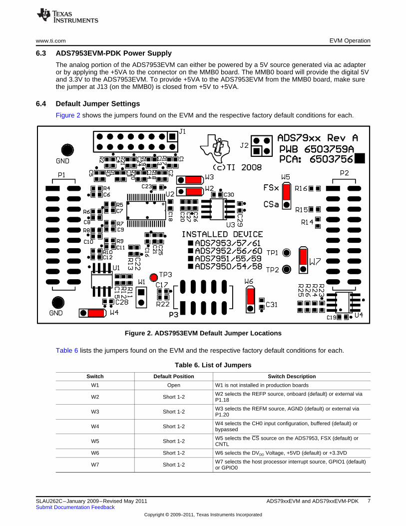
6.4 Default Jumper Settings
Figure 2 shows the jumpers found on the EVM and the respective factory default conditions for each.
Figure 2. ADS7953EVM Default Jumper Locations
Table 6 lists the jumpers found on the EVM and the respective factory default conditions for each.
Table 6. List of Jumpers
Switch Default Position Switch Description
W1 Open W1 is not installed in production boards
W2 selects the REFP source, onboard (default) or external viaW2 Short 1-2 P1.18
W3 selects the REFM source, AGND (default) or external viaW3 Short 1-2 P1.20
W4 selects the CH0 input configuration, buffered (default) orW4 Short 1-2 bypassed
W5 selects the CS source on the ADS7953, FSX (default) orW5 Short 1-2 CNTL
W6 Short 1-2 W6 selects the DVDD Voltage, +5VD (default) or +3.3VD
W7 selects the host processor interrupt source, GPIO1 (default)W7 Short 1-2 or GPIO0
7SLAU262C–January 2009–Revised May 2011 ADS79xxEVM and ADS79xxEVM-PDKSubmit Documentation Feedback
Copyright © 2009–2011, Texas Instruments Incorporated

ADS7953EVM-PDK Kit Operation www.ti.com
7 ADS7953EVM-PDK Kit Operation
This section provides information on using the ADS7953EVM-PDK, including setup, program installation,and program usage.
To prepare to evaluate the ADS7953 with the ADS7953EVM-PDK, complete the following steps:
Step 1. Install the ADCPro software (if not already installed) on a PC.
Step 2. Install the ADS7953EVM-PDK EVM plug-in software.
Step 3. Set up the ADS7953EVM-PDK.
Step 4. Connect a proper power supply or use the included AC adapter.
Step 5. Complete the NI-VISA USB driver installation process.
Step 6. Run the ADCPro software.
Step 7. Complete the Microsoft Windows USB driver installation process.
Each task is described in the subsequent sections of this document.
7.1 Installing the ADCPro Software
CAUTION
Do not connect the ADS7953EVM-PDK before installing the software on asuitable PC. Failure to observe this caution may cause Microsoft Windows tonot recognize the ADS7953EVM-PDK.
The latest software is available from the TI website at http://www.ti.com/. The ADCPro installer will checkfor updates when executed (if connected to the Internet), and then gives the option of downloading andinstalling the latest version. See the ADCPro Analog-to-Digital Converter Evalutation Software UsersGuide for instructions on installing and using ADCPro.
To install the ADS7953EVM-PDK plug-in, run the file: ads7953evm-pdk-plugin-1.1.0.exe (1.1.0 is theversion number, and increments with software version releases). Double-click the file to run it; then followthe instructions shown. Also, use the ADCPro Update Check feature to check for newer versions of theADS7953EVM-PDK plug-in, once one version has been installed.
The software should now be installed, but the USB drivers may not have been loaded by the PC operatingsystem. This step will complete when the ADCPro software is executed.
7.2 Setting Up the ADS7953EVM-PDK
The ADS7953EVM-PDK contains both the ADS7953EVM and the MMB0 motherboard; however, thedevices are shipped unconnected. Follow these steps to set up the ADS7953EVM-PDK:
Step 1. Unpack the ADS7953EVM-PDK kit.
Step 2. Set the jumpers and switches on the MMB0 as shown in Figure 3.
• Set the Boot Mode switch to USB.• Connect +5V and +5VA on jumper block J13 (if +5V is supplied from J14 +5VA).• Leave +5V and +VA disconnected on jumper block J13.• If the PDK will be powered from an ac adapter, connect J12. If the PDK will be powered through the
terminal block, disconnect J12 (see Section 7.3 of this document for additional power supplyconnection details).
8 ADS79xxEVM and ADS79xxEVM-PDK SLAU262C–January 2009–Revised May 2011Submit Documentation Feedback
Copyright © 2009–2011, Texas Instruments Incorporated

www.ti.com ADS7953EVM-PDK Kit Operation
Figure 3. MMB0 Initial Setup
Step 3. Plug the ADS7953EVM into the MMB0. The female portion of P1, P2 and P3 on the EVM alignwith male connectors J7, J4 and J5 respective on the MMB0.
CAUTION Do not misalign the pins when plugging the ADS7953EVM into the MMB0. Check the pinalignment of P1, P2, and P3 carefully before applying power to the PDK.
Step 4. Verify the jumpers on the ADS7953EVM are as shown in Figure 2 (note that these settings are thefactory-configured settings for the EVM).
7.2.1 About the MMB0
The MMB0 is a Modular EVM System motherboard. It is designed around the TMS320VC5507, a DSPwith an onboard USB interface from Texas Instruments. The MMB0 also has 16MB of SDRAM installed.
The MMB0 is not intended to be used as a DSP development board, and it is not available separately. TIcannot offer support for the MMB0 except as part of an EVM-PDK kit. For schematics or other informationabout the MMB0, contact Texas Instruments.
7.3 Connecting the Power Supply
The ADS7953EVM-PDK can be operated with a unipolar +5V supply or a combination of +5V and +3.3Vsupplies.
When the MMB0 DSP is powered properly, LED D2 glows green. The green light indicates that the 3.3Vsupply for the MMB0 is operating properly. (It does not indicate that the EVM power supplies areoperating properly.)
9SLAU262C–January 2009–Revised May 2011 ADS79xxEVM and ADS79xxEVM-PDKSubmit Documentation Feedback
Copyright © 2009–2011, Texas Instruments Incorporated

ADS7953EVM-PDK Kit Operation www.ti.com
7.3.1 Connecting an AC Adapter
An ac adapter can be connected to barrel jack J2 on the MMB0. J2 is located next to the USB connector.The adapter must output 6V-7V dc. The connector must be sleeve-negative, tip-positive. It should have acurrent rating of at least 2A.
Jumper J12 on the MMB0 connects a wall-mounted power supply to the board. To use the wall-mountsupply, J12 must be shorted. Figure 4 illustrates how to connect an ac adapter to the MMB0.
Figure 4. Connecting an AC Adapter
7.3.2 Connecting a Laboratory Power Supply
A laboratory power supply can be connected through terminal block J14 on the MMB0, as shown inFigure 5.
To use a unipolar lab power supply configuration:
• Disconnect J12 on the MMB0.• Connect a +5V dc supply to the +5VD terminal on J14.• Connect ground of the dc supply to the GND terminal on J14.
It is not necessary to connect a +5V dc supply voltage to the +5VA terminal on J14 if the +5V/+5VAposition on J13 is shorted.
10 ADS79xxEVM and ADS79xxEVM-PDK SLAU262C–January 2009–Revised May 2011Submit Documentation Feedback
Copyright © 2009–2011, Texas Instruments Incorporated

www.ti.com ADS7953EVM-PDK Kit Operation
Figure 5. Laboratory Power-Supply Connection
7.4 Running the Software and Completing Driver Installation
Note: The software is continually under development. These instructions and screen images are current atthe time of this writing, but may not exactly match future releases.
The program for evaluating the ADS7953EVM-PDK is called ADCPro. This program uses plug-ins tocommunicate with the EVM. The ADS7953EVM-PDK plug-in is included in the ADS7953EVM-PDKpackage.
The program currently runs only on Microsoft Windows platforms of Windows XP; Windows Vista is NOTsupported at the time of this writing.
If this is the first time installing ADCPro and the EVM plug-ins, follow these procedures to run ADCPro andcomplete the necessary driver installation.
7.4.1 NI-VISA USB Device Driver Installation1. After the ADCPro software is installed, apply power to the PDK and connect the board to an available
PC USB port.2. The computer should recognize new hardware and begin installing the drivers for the hardware.
Figure 6 through Figure 10 are provided for reference to show the installation steps.
• For the first screen, Figure 6, it is not necessary to search for the software; it has already beeninstalled to the PC.
• For the remaining steps, accept the default settings.
11SLAU262C–January 2009–Revised May 2011 ADS79xxEVM and ADS79xxEVM-PDKSubmit Documentation Feedback
Copyright © 2009–2011, Texas Instruments Incorporated

ADS7953EVM-PDK Kit Operation www.ti.com
Figure 6. NI-VISA Driver Installation
Figure 7. NI-VISA Driver Installation Question
12 ADS79xxEVM and ADS79xxEVM-PDK SLAU262C–January 2009–Revised May 2011Submit Documentation Feedback
Copyright © 2009–2011, Texas Instruments Incorporated

www.ti.com ADS7953EVM-PDK Kit Operation
Figure 8. NI-VISA Driver Installing
Figure 9. NI-VISA Driver Complete Installation
13SLAU262C–January 2009–Revised May 2011 ADS79xxEVM and ADS79xxEVM-PDKSubmit Documentation Feedback
Copyright © 2009–2011, Texas Instruments Incorporated

ADS7953EVM-PDK Kit Operation www.ti.com
This procedure should complete the installation of the NI-VISA drivers. Verify the proper installation byopening the Device Manager and locating as shown in Figure 10.
Figure 10. NI-VISA Driver Verification Using Device Manager
Once ADCPro is installed, install the ADS7953EVM-PDK software to allow ADCPro to recognize theevaluation board.
7.4.2 USBStyx Driver Installation
Start the software by selecting ADCPro from the Windows Start menu. The screen in Figure 11 appears.
Figure 11. ADCPro Software Start-up Display Window
1. Select ADS7953EVM from the EVM drop-down menu. The ADS7953EVM-PDK plugin appears in theleft pane, as shown in Figure 12.
14 ADS79xxEVM and ADS79xxEVM-PDK SLAU262C–January 2009–Revised May 2011Submit Documentation Feedback
Copyright © 2009–2011, Texas Instruments Incorporated

www.ti.com ADS7953EVM-PDK Kit Operation
Figure 12. ADS7953EVM-PDK Plug-In Display Window
2. The ADS7953EVM-PDK plug-in window has a status area at the top of the screen. When the plug-in isfirst loaded, the plug-in searches for the board. The user will see a series of messages in the statusarea indicating this action.
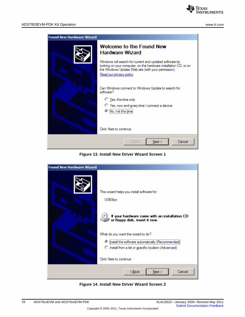
3. If the operating system drivers have not been loaded, Windows will display the Windows Install NewDriver Wizard sequence (illustrated in Figure 13 through Figure 17). Accept the default settings.
• NOTE: During the driver installation, a message may appear indicating the firmware load hasTIMED OUT. Click OK and continue driver installation. The plug-in will attempt to download thefirmware again once the driver installation completes.
15SLAU262C–January 2009–Revised May 2011 ADS79xxEVM and ADS79xxEVM-PDKSubmit Documentation Feedback
Copyright © 2009–2011, Texas Instruments Incorporated
ADS7953EVM-PDK Kit Operation www.ti.com
Figure 13. Install New Driver Wizard Screen 1
Figure 14. Install New Driver Wizard Screen 2
16 ADS79xxEVM and ADS79xxEVM-PDK SLAU262C–January 2009–Revised May 2011Submit Documentation Feedback
Copyright © 2009–2011, Texas Instruments Incorporated

www.ti.com ADS7953EVM-PDK Kit Operation
Figure 15. Install New Driver Wizard Screen 3
Figure 16. Install New Driver Wizard Screen 4
17SLAU262C–January 2009–Revised May 2011 ADS79xxEVM and ADS79xxEVM-PDKSubmit Documentation Feedback
Copyright © 2009–2011, Texas Instruments Incorporated
ADS7953EVM-PDK Kit Operation www.ti.com
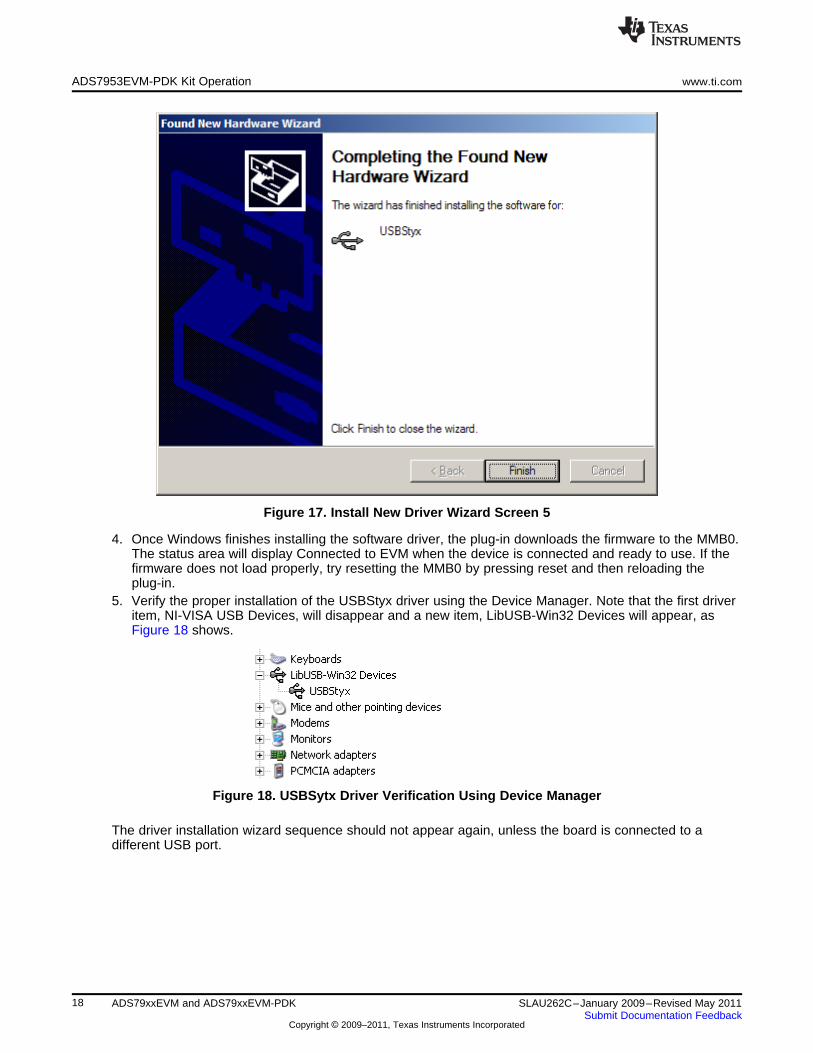
Figure 17. Install New Driver Wizard Screen 5
4. Once Windows finishes installing the software driver, the plug-in downloads the firmware to the MMB0.The status area will display Connected to EVM when the device is connected and ready to use. If thefirmware does not load properly, try resetting the MMB0 by pressing reset and then reloading theplug-in.
5. Verify the proper installation of the USBStyx driver using the Device Manager. Note that the first driveritem, NI-VISA USB Devices, will disappear and a new item, LibUSB-Win32 Devices will appear, asFigure 18 shows.
Figure 18. USBSytx Driver Verification Using Device Manager
The driver installation wizard sequence should not appear again, unless the board is connected to adifferent USB port.
18 ADS79xxEVM and ADS79xxEVM-PDK SLAU262C–January 2009–Revised May 2011Submit Documentation Feedback
Copyright © 2009–2011, Texas Instruments Incorporated

www.ti.com Evaluating Performance with the ADCPro Software
8 Evaluating Performance with the ADCPro Software
The evaluation software is based on ADCPro, a program that operates using a variety of plug-ins. (TheADS7953EVM plug-in is installed as described in the previous section.)
To use ADCPro, load an EVM plug-in and a test plug-in. To load an EVM plug-in, select it from the EVMmenu. To load a test plug-in, select it from the Test menu. To unload a plug-in, select the Unload optionfrom the corresponding menu.
Only one of each kind of plug-in can be loaded at a time. If selecting a different plugin, the previous pluginis unloaded.
8.1 Using the ADS7953EVM-PDK Plug-in
The ADS7953EVM-PDK plug-in for ADCPro provides complete control over all settings of the ADS7953. Itconsists of a tabbed interface (see Figure 19), with different functions available on different tabs. Thesecontrols are described in this section.
The user can adjust the ADS7953EVM settings when not acquiring data. During acquisition, all controlsare disabled and settings may not be changed.
When a setting is changed on the ADS7953EVM plug-in, the setting immediately updates on the board.
Settings on the ADS7953EVM correspond to settings described in the ADS7953 product data sheet; seethe ADS7953 data sheet for details.
Because the effective sampling rate of the ADS7953 depends upon settings of the Clock Freq and thenumber of channels being sampled, the Sampling Rate indicator in the upper right corner of the plug-ininterface is always visible and updates whenever a setting changes that affects the effective 'per-channel'sampling rate.
19SLAU262C–January 2009–Revised May 2011 ADS79xxEVM and ADS79xxEVM-PDKSubmit Documentation Feedback
Copyright © 2009–2011, Texas Instruments Incorporated

Evaluating Performance with the ADCPro Software www.ti.com
8.1.1 Channel Tab
The ADS7953 can acquire from one to sixteen channels sequentially or in a user defined pattern. TheChannel Tab (as shown in Figure 19) provides the control to turn each channel on or off. By default,manual channel mode is enabled. In manual mode, any single channel may be selected for conversion.
Figure 19. Channel Enable
20 ADS79xxEVM and ADS79xxEVM-PDK SLAU262C–January 2009–Revised May 2011Submit Documentation Feedback
Copyright © 2009–2011, Texas Instruments Incorporated

www.ti.com Evaluating Performance with the ADCPro Software
In addition, the Manual Control button (shown in Figure 20) can be used to enable or disable auto scanmodes 1 and 2. Auto 1 Mode allows the selection of any number of channels from the channel selectionlist. Auto 2 Mode allows the selection of the highest channel to convert. All channels below this will beconverted once this selection is made by pressing the 'Accept Selection' button.
Figure 20. Manual Channel Control
21SLAU262C–January 2009–Revised May 2011 ADS79xxEVM and ADS79xxEVM-PDKSubmit Documentation Feedback
Copyright © 2009–2011, Texas Instruments Incorporated

Evaluating Performance with the ADCPro Software www.ti.com
8.1.2 Other Tab
The ADS7953 requires a clock to operate. The maximum frequency is selected by default for the differentoperating modes, providing the maximum 1MSPS throughput rate specified in the datasheet.
The clock setting can be modified in this tab by accepting the default SPI or clock stop mode, acontinuous clock mode with the fastest possible serial clock, or a continuous clock mode with a variablefrequency.
The analog input range can also be specified in this tab as well as the contents of the four MSBs ofchannel data (GPIO status or Channel Address of the conversion results).
Figure 21. Serial Clock, Input Range and MS Nibble settings
22 ADS79xxEVM and ADS79xxEVM-PDK SLAU262C–January 2009–Revised May 2011Submit Documentation Feedback
Copyright © 2009–2011, Texas Instruments Incorporated

www.ti.com Evaluating Performance with the ADCPro Software
8.1.3 Alarm Tab
The ADS7953 offers configurable alarm outputs for both high and low alarm selections. The configurationof the alarm function takes place in two steps, the first of which is the setting of the alarm limits. In theAlarm Tab, the hex values for high and low limits are entered for each channel requiring the alarmfunction. To enable the alarm functions, the GPIO Function tab must be considered next.
Figure 22. High and Low Alarm Limits by Channel
23SLAU262C–January 2009–Revised May 2011 ADS79xxEVM and ADS79xxEVM-PDKSubmit Documentation Feedback
Copyright © 2009–2011, Texas Instruments Incorporated

Evaluating Performance with the ADCPro Software www.ti.com
8.1.4 GPIO Function Tab
The GPIO0, GPIO1, GPIO2 and GPIO3 pins on the ADS7953 can function as simple general purposeinputs/outputs or as specialized control and monitor functions. The alarm function described in theprevious section is processed by GPIO0 and GPIO1. Refer to the data sheet for specific details on GPIO0and GPIO1 options. GPIO2 can be used to configure the input range of the ADS7953 (2.5V max or 5.0Vmax), and GPIO3 can be used as a power down input pin.
Figure 23. GPIO and System Monitor Control options
24 ADS79xxEVM and ADS79xxEVM-PDK SLAU262C–January 2009–Revised May 2011Submit Documentation Feedback
Copyright © 2009–2011, Texas Instruments Incorporated

www.ti.com Evaluating Performance with the ADCPro Software
8.1.5 GPIO Tab
The GPIO Tab provides a means to monitor and control GPIO functions. If a GPIO is selected in the GPIOFunction tab to perform a specialized function, it will appear 'grayed out' in the GPIO tab. For pinsconfigured as GP outputs, a push button will enable the user to set the desired output state. GP Inputs aremonitored with an LED display (bright green = logic high).
Figure 24. GPIO selection, controls and indicators
25SLAU262C–January 2009–Revised May 2011 ADS79xxEVM and ADS79xxEVM-PDKSubmit Documentation Feedback
Copyright © 2009–2011, Texas Instruments Incorporated
Schematic and Bill of Materials www.ti.com
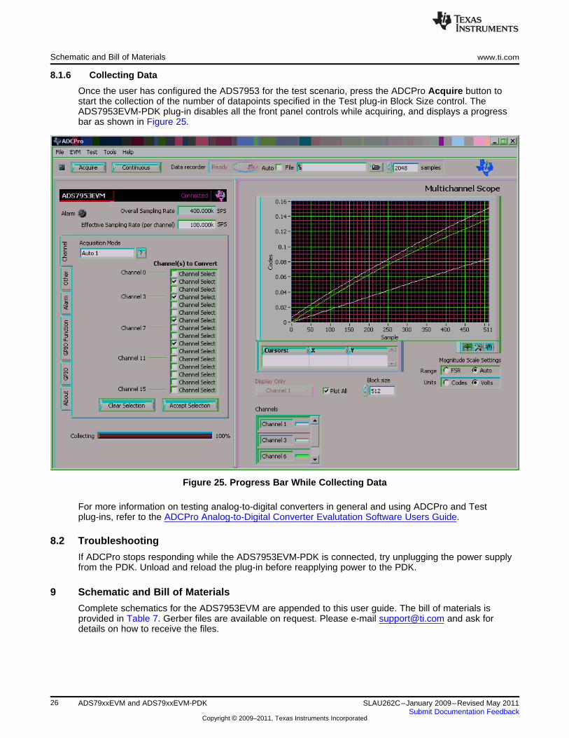
8.1.6 Collecting Data
Once the user has configured the ADS7953 for the test scenario, press the ADCPro Acquire button tostart the collection of the number of datapoints specified in the Test plug-in Block Size control. TheADS7953EVM-PDK plug-in disables all the front panel controls while acquiring, and displays a progressbar as shown in Figure 25.
Figure 25. Progress Bar While Collecting Data
For more information on testing analog-to-digital converters in general and using ADCPro and Testplug-ins, refer to the ADCPro Analog-to-Digital Converter Evalutation Software Users Guide.
8.2 Troubleshooting
If ADCPro stops responding while the ADS7953EVM-PDK is connected, try unplugging the power supplyfrom the PDK. Unload and reload the plug-in before reapplying power to the PDK.
9 Schematic and Bill of Materials
Complete schematics for the ADS7953EVM are appended to this user guide. The bill of materials isprovided in Table 7. Gerber files are available on request. Please e-mail [email protected] and ask fordetails on how to receive the files.
26 ADS79xxEVM and ADS79xxEVM-PDK SLAU262C–January 2009–Revised May 2011Submit Documentation Feedback
Copyright © 2009–2011, Texas Instruments Incorporated

+V
CC
W2
R5
33
AG
ND
R13
33
AG
ND
R6
33
AG
ND
R4
33
AG
ND
R3
33
AG
ND
R2
33
AG
ND
R7
33
AG
ND
R8
33
AG
ND
R9
33
AG
ND
R10
33
AG
ND
R1
33
AG
ND
W4
CH
0
CH
1
CH
2
CH
3
CH
4
CH
5
CH
6
CH
7
CH
15
CH
14
CH
13
RE
F+
W3
RE
F-
AG
ND
-In
2
+In
3
Outp
ut
6
7 4
U1
OP
A365
R11
NI
R12
0
AG
ND
CH
0
C2
3
0.1
uF
C17
10uF
AG
ND
CH
10
CH
9
CH
8
CH
7
CH
6
AG
ND
VR
EF
+
INT
AG
ND
C12
270pF
C11
270pF
C10
270pF
C9
270pF
C8
270pF
C7
270pF
C6
270pF
C5
270pF
C4
270pF
C3
270pF
C15
NI
C2
2
270pF
C21
10uF
C25
0.1
uF
DG
ND
R15 33
SD
O
SD
I
W1
SC
LK
1357911
13
17
19
2468
10
12
14
16
18
20
15
P1
1 3 5 7 9 11
13
17
19
2 4 6 8
10
12
14
16
18
20
15
P2
C19
0.1
uF
C18
10uF
C20
1.0
uF
RE
F_M
TP
3
1 23 45 67 89 10
P3B
R16
33
R14 33
CS
*
CLK
X
FS
X
GP
IO2
1
GP
IO3
2
AG
ND
/RE
FM
3
RE
FP
4
+V
A5
AG
ND
6
MX
D7
AIN
P8
AG
ND
/AIN
M9
NC
/Ch15
11
NC
/Ch14
12
AG
ND
20
AG
ND
10
NC
/Ch13
13
NC
/Ch12
14
Ch
11
15
Ch
10
16
Ch9
17
Ch8
18
AG
ND
19
Ch7
21
Ch6
22
Ch5
23
Ch4
24
Ch3
25
Ch2
26
Ch1
27
Ch0
28
VC
C29
CS
31
SC
LK
32
VE
E30
SD
I33
SD
O34
BD
GN
D35
+V
BD
36
GP
IO0
37
GP
IO1
38
U2
AD
S79X
X
+V
CC
+V
CC
C26
10uF
Ch0_F
LT
W6
C16
0.1
uF
Ch0_F
LT
Ch1_F
LT
Ch2_F
LT
Ch3_F
LT
Ch4_F
LT
Ch5_F
LT
SD
O
SD
I
CH
12
CH
11
CH
10
CH
9
CH
8
Ch1_F
LT
Ch2_F
LT
Ch3_F
LT
Ch4_F
LT
Ch5_F
LT
R21
33
AG
ND
CH
11
C2
4
270pF
R17
33
AG
ND
CH
15
C1
270pF
R18
33
AG
ND
CH
14
C2
270pF
R19
33
AG
ND
CH
13
C1
3
270pF
R20
33
AG
ND
CH
12
C1
4
270pF
RE
F_M
TP
1
+V
CC
12
34
J2
RE
F_P
TP
2
VR
EF
+R
EF
_P
RE
F+
RE
F-
Vo
6
Trim
5
Tem
p3
GN
D4
Vin
2
NC
1
NC
7
NC
8
U3
RE
F5025
GN
DG
ND
12
34
56
78
910
11
12
13
14
15
16
J1
8X
2X
.1
R22
10
C27
10uF
+V
CC
VC
C_D
VC
C_
D
C29
1.0
uF
C28
1.0
uF
A0
1
A1
2
A2
3
GN
D4
SD
A5
SC
L6
WP
7
VC
C8
U4
MC
P_24LC
256
R24
NI
R2
333
VC
C_D
R25
47.5
KR
26
47.5
K
VC
C_D
W7
W5
C31
10uF
C30
1.0
uF
VC
C_D
www.ti.com Schematic and Bill of Materials
Figure 26. ADS7953EVM Schematic
27SLAU262C–January 2009–Revised May 2011 ADS79xxEVM and ADS79xxEVM-PDKSubmit Documentation Feedback
Copyright © 2009–2011, Texas Instruments Incorporated

Schematic and Bill of Materials www.ti.com
9.1 Bill of Materials
Note: All components should be compliant with the European Union Restriction on Use of HazardousSubstances (RoHS) Directive. Some part numbers may be either leaded or RoHS. Verify that purchasedcomponents are RoHS-compliant. (For more information about TI's position on RoHS compliance, see theTI website.)
Table 7. ADS7953EVM Bill of Materials
Item No. Qty Ref Des Description Vendor Part Number
1 1 N/A Printed Wiring TIBoard
2 0 C15 Not Installed
3 0 R11 R14 R24 Not Installed
4 16 C1 - C14 C22 C24 CAP CER 270PF TDK C1608C0G1H271J50V C0G 5% 0603
5 4 C16 C19 C23 C25 CAP CER 0.10UF TDK C1608X7R1E104K25V X7R 10% 0603
6 6 C17 C18 C21 C26 CAP CERAMIC Panasonic ECJ-1VB0J106MC27 10UF 6.3V X5R
0603
7 4 C20 C28 C29 C30 CAP CER 1.0UF Taiyo Yuden EMK107B7105KA-T16V X7R 0603
8 1 J1 8X2X.1 Header Samtec TMS-108-02-G-D
9 1 J2 2X2X.1 Header Samtec TMS-102-02-G-S
10 2 P1 P2 (top side) 10 Pin, Dual Row, Samtec TSM-110-01-T-DV-SMT Header (20 P P
11 2 P1B P2B (bottom 10 Pin, Dual Row, Samtec SSW-110-22-F-D-side) SMT Socket (20 P VS-K
12 1 P3 (top side) 5 Pin, Dual Row, Samtec TSM-105-01-T-DV-SMT Header (10 Po P
13 1 P3B (bottom side) 5 Pin, Dual Row, Samtec SSW-105-22-F-D-SMT Socket (10 Po VS-K
14 19 R1 - R10 R13 R15 - RES 33.0 OHM Yageo RC0603FR-0733RL1/10W 1% 0603SMD
15 1 R12 RES 0.0 OHM Yageo RC0603JR-070RL1/10W 5% 0603SMD
16 1 R22 RES 10.0 OHM Yageo RC0603FR-0710RL1/10W 1% 0603SMD
17 2 R25 R26 RES 47.5K OHM Yageo RC0603FR-1/10W 1% 0603 0747K5LSMD
18 3 TP1 TP2 TP3 TEST POINT PC Keystone 5001MINI .040D RED
19 2 GND GND TEST POINT PC Keystone 5011MULTI PURPOSEBLK
20 1 U1 2.2V, 50MHz, TI OPA365AIDLow-Noise,Single-Sup
21 1 U2 12/10/8-Bit, 1 TI ADS7953/52/51/50MSPS,16/12/8/4-Cha
22 1 U3 Low-Noise, Very TI REF5025IDLow Drift, Precisi
23 1 U4 IC SERIAL Microchip 24LC256T-I/SNEEPROM 256K2.5V 8-SOIC
28 ADS79xxEVM and ADS79xxEVM-PDK SLAU262C–January 2009–Revised May 2011Submit Documentation Feedback
Copyright © 2009–2011, Texas Instruments Incorporated

www.ti.com Revision History
Table 7. ADS7953EVM Bill of Materials (continued)
Item No. Qty Ref Des Description Vendor Part Number
24 0 W1 Not Installed Samtec TMS-102-02-G-S
25 6 W2 - W7 3 Pin , 2mm Header Samtec TMM-103-01-T-S
Revision History
Changes from B Revision (March, 2011) to C Revision ................................................................................................. Page
• Updated Table 5 .......................................................................................................................... 6
NOTE: Page numbers for previous revisions may differ from page numbers in the current version.
29SLAU262C–January 2009–Revised May 2011 Revision HistorySubmit Documentation Feedback
Copyright © 2009–2011, Texas Instruments Incorporated

1 2 3 4 5 6
A
B
C
D
654321
D
C
B
A
ti12500 TI Boulevard. Dallas, Texas 75243
Title:
SHEET: OF:FILE: SIZE:DATE:
REV:
17-Nov-2008
Drawn By:
Engineer:
Revision History
REV ECN Number Approved
ADS795x_A.sch
DOCUMENTCONTROL #
+VCC
W2
R5
33
AGND
R13
33
AGND
R6
33
AGND
R4
33
AGND
R3
33
AGND
R2
33
AGND
R7
33
AGND
R8
33
AGND
R9
33
AGND
R10
33
AGND
R1
33
AGND
W4
CH0
CH1
CH2
CH3
CH4
CH5
CH6
CH7
CH15
CH14
CH13
REF+
W3
REF-
AGND
-In2
+In3
Output6
74
U1OPA365
R11
NIR12
0
AGND
CH0
C23
0.1uF
C17
10uF
AGND
CH10
CH9
CH8
CH7
CH6
AGND
VREF+
INTAGND
1
1 1
Tom Hendrick
C12
270pF
C11
270pF
C10
270pF
C9
270pF
C8
270pF
C7
270pF
C6
270pF
C5
270pF
C4
270pF
C3
270pF
C15
NI
C22
270pF
C21
10uF
C25
0.1uF
DGND
R15
33
SDO
SDI
W1
SCLK1
3
5
7
9
11
13
17
19
2
4
6
8
10
12
14
16
18
20
15
P1
1
3
5
7
9
11
13
17
19
2
4
6
8
10
12
14
16
18
20
15
P2
C190.1uF
C18
10uF
C20
1.0uF
REF_M
ADS79xx Evaluation Module
TP3
12
34
56
78
910
P3B
R16
33
R14
33
CS*
CLKX
FSX
GPIO21
GPIO32
AGND/REFM3
REFP4
+VA5
AGND6
MXD7
AINP8
AGND/AINM9
NC/Ch1511
NC/Ch1412
AGND20
AGND10
NC/Ch1313
NC/Ch1214
Ch1115
Ch1016
Ch917
Ch818
AGND19
Ch721
Ch622
Ch523
Ch424
Ch325
Ch226
Ch127
Ch028
VCC29
CS31
SCLK32
VEE30
SDI33
SDO34
BDGND35
+VBD36
GPIO037
GPIO138
U2
ADS79XX
+VCC
+VCC C26
10uF
Ch0_FLT
W6
C16
0.1uF
Ch0_FLT
Ch1_FLT
Ch2_FLT
Ch3_FLT
Ch4_FLT
Ch5_FLT
SDO
SDI
CH12
CH11
CH10
CH9
CH8
Ch1_FLT
Ch2_FLT
Ch3_FLT
Ch4_FLT
Ch5_FLT
R21
33
AGND
CH11
C24
270pF
R17
33
AGND
CH15
C1
270pF
R18
33
AGND
CH14
C2
270pF
R19
33
AGND
CH13
C13
270pF
R20
33
AGND
CH12
C14
270pF
REF_M
TP1
+VCC
1 2
3 4
J2
REF_P
TP2
VREF+ REF_P
REF+
REF-
Vo6
Trim5
Temp3
GND4
Vin2
NC1
NC7
NC8
U3
REF5025
GNDGND
1 23 45 67 89 1011 1213 1415 16
J1
8X2X.1
R22
10
C27
10uF
+VCC
VCC_D
VCC_D
C29
1.0uF
C28
1.0uF
A01
A12
A23
GND4
SDA5
SCL6
WP7
VCC8
U4
MCP_24LC256
R24
NI
R2333
VCC_D
R2547.5K
R2647.5K
VCC_D
W7
W5
C31
10uF
C30
1.0uF
VCC_D
6503756Lisa Parker
Evaluation Board/Kit Important Notice
Texas Instruments (TI) provides the enclosed product(s) under the following conditions:
This evaluation board/kit is intended for use for ENGINEERING DEVELOPMENT, DEMONSTRATION, OR EVALUATIONPURPOSES ONLY and is not considered by TI to be a finished end-product fit for general consumer use. Persons handling theproduct(s) must have electronics training and observe good engineering practice standards. As such, the goods being provided arenot intended to be complete in terms of required design-, marketing-, and/or manufacturing-related protective considerations,including product safety and environmental measures typically found in end products that incorporate such semiconductorcomponents or circuit boards. This evaluation board/kit does not fall within the scope of the European Union directives regardingelectromagnetic compatibility, restricted substances (RoHS), recycling (WEEE), FCC, CE or UL, and therefore may not meet thetechnical requirements of these directives or other related directives.
Should this evaluation board/kit not meet the specifications indicated in the User’s Guide, the board/kit may be returned within 30days from the date of delivery for a full refund. THE FOREGOING WARRANTY IS THE EXCLUSIVE WARRANTY MADE BYSELLER TO BUYER AND IS IN LIEU OF ALL OTHER WARRANTIES, EXPRESSED, IMPLIED, OR STATUTORY, INCLUDINGANY WARRANTY OF MERCHANTABILITY OR FITNESS FOR ANY PARTICULAR PURPOSE.
The user assumes all responsibility and liability for proper and safe handling of the goods. Further, the user indemnifies TI from allclaims arising from the handling or use of the goods. Due to the open construction of the product, it is the user’s responsibility totake any and all appropriate precautions with regard to electrostatic discharge.
EXCEPT TO THE EXTENT OF THE INDEMNITY SET FORTH ABOVE, NEITHER PARTY SHALL BE LIABLE TO THE OTHERFOR ANY INDIRECT, SPECIAL, INCIDENTAL, OR CONSEQUENTIAL DAMAGES.
TI currently deals with a variety of customers for products, and therefore our arrangement with the user is not exclusive.
TI assumes no liability for applications assistance, customer product design, software performance, or infringement ofpatents or services described herein.
Please read the User’s Guide and, specifically, the Warnings and Restrictions notice in the User’s Guide prior to handling theproduct. This notice contains important safety information about temperatures and voltages. For additional information on TI’senvironmental and/or safety programs, please contact the TI application engineer or visit www.ti.com/esh.
No license is granted under any patent right or other intellectual property right of TI covering or relating to any machine, process, orcombination in which such TI products or services might be or are used.
FCC Warning
This evaluation board/kit is intended for use for ENGINEERING DEVELOPMENT, DEMONSTRATION, OR EVALUATIONPURPOSES ONLY and is not considered by TI to be a finished end-product fit for general consumer use. It generates, uses, andcan radiate radio frequency energy and has not been tested for compliance with the limits of computing devices pursuant to part 15of FCC rules, which are designed to provide reasonable protection against radio frequency interference. Operation of thisequipment in other environments may cause interference with radio communications, in which case the user at his own expensewill be required to take whatever measures may be required to correct this interference.
EVM Warnings and Restrictions
It is important to operate this EVM within the input voltage range of 3.3 V to +5 V and the output voltage range of 0 V to +5 V.
Exceeding the specified input range may cause unexpected operation and/or irreversible damage to the EVM. If there arequestions concerning the input range, please contact a TI field representative prior to connecting the input power.
Applying loads outside of the specified output range may result in unintended operation and/or possible permanent damage to theEVM. Please consult the EVM User's Guide prior to connecting any load to the EVM output. If there is uncertainty as to the loadspecification, please contact a TI field representative.
During normal operation, some circuit components may have case temperatures greater than +30°C. The EVM is designed tooperate properly with certain components above +85°C as long as the input and output ranges are maintained. These componentsinclude but are not limited to linear regulators, switching transistors, pass transistors, and current sense resistors. These types ofdevices can be identified using the EVM schematic located in the EVM User's Guide. When placing measurement probes nearthese devices during operation, please be aware that these devices may be very warm to the touch.
Mailing Address: Texas Instruments, Post Office Box 655303, Dallas, Texas 75265Copyright © 2011, Texas Instruments Incorporated

IMPORTANT NOTICE
Texas Instruments Incorporated and its subsidiaries (TI) reserve the right to make corrections, modifications, enhancements, improvements,and other changes to its products and services at any time and to discontinue any product or service without notice. Customers shouldobtain the latest relevant information before placing orders and should verify that such information is current and complete. All products aresold subject to TI’s terms and conditions of sale supplied at the time of order acknowledgment.
TI warrants performance of its hardware products to the specifications applicable at the time of sale in accordance with TI’s standardwarranty. Testing and other quality control techniques are used to the extent TI deems necessary to support this warranty. Except wheremandated by government requirements, testing of all parameters of each product is not necessarily performed.
TI assumes no liability for applications assistance or customer product design. Customers are responsible for their products andapplications using TI components. To minimize the risks associated with customer products and applications, customers should provideadequate design and operating safeguards.
TI does not warrant or represent that any license, either express or implied, is granted under any TI patent right, copyright, mask work right,or other TI intellectual property right relating to any combination, machine, or process in which TI products or services are used. Informationpublished by TI regarding third-party products or services does not constitute a license from TI to use such products or services or awarranty or endorsement thereof. Use of such information may require a license from a third party under the patents or other intellectualproperty of the third party, or a license from TI under the patents or other intellectual property of TI.
Reproduction of TI information in TI data books or data sheets is permissible only if reproduction is without alteration and is accompaniedby all associated warranties, conditions, limitations, and notices. Reproduction of this information with alteration is an unfair and deceptivebusiness practice. TI is not responsible or liable for such altered documentation. Information of third parties may be subject to additionalrestrictions.
Resale of TI products or services with statements different from or beyond the parameters stated by TI for that product or service voids allexpress and any implied warranties for the associated TI product or service and is an unfair and deceptive business practice. TI is notresponsible or liable for any such statements.
TI products are not authorized for use in safety-critical applications (such as life support) where a failure of the TI product would reasonablybe expected to cause severe personal injury or death, unless officers of the parties have executed an agreement specifically governingsuch use. Buyers represent that they have all necessary expertise in the safety and regulatory ramifications of their applications, andacknowledge and agree that they are solely responsible for all legal, regulatory and safety-related requirements concerning their productsand any use of TI products in such safety-critical applications, notwithstanding any applications-related information or support that may beprovided by TI. Further, Buyers must fully indemnify TI and its representatives against any damages arising out of the use of TI products insuch safety-critical applications.
TI products are neither designed nor intended for use in military/aerospace applications or environments unless the TI products arespecifically designated by TI as military-grade or "enhanced plastic." Only products designated by TI as military-grade meet militaryspecifications. Buyers acknowledge and agree that any such use of TI products which TI has not designated as military-grade is solely atthe Buyer's risk, and that they are solely responsible for compliance with all legal and regulatory requirements in connection with such use.
TI products are neither designed nor intended for use in automotive applications or environments unless the specific TI products aredesignated by TI as compliant with ISO/TS 16949 requirements. Buyers acknowledge and agree that, if they use any non-designatedproducts in automotive applications, TI will not be responsible for any failure to meet such requirements.
Following are URLs where you can obtain information on other Texas Instruments products and application solutions:
Products Applications
Audio www.ti.com/audio Communications and Telecom www.ti.com/communications
Amplifiers amplifier.ti.com Computers and Peripherals www.ti.com/computers
Data Converters dataconverter.ti.com Consumer Electronics www.ti.com/consumer-apps
DLP® Products www.dlp.com Energy and Lighting www.ti.com/energy
DSP dsp.ti.com Industrial www.ti.com/industrial
Clocks and Timers www.ti.com/clocks Medical www.ti.com/medical
Interface interface.ti.com Security www.ti.com/security
Logic logic.ti.com Space, Avionics and Defense www.ti.com/space-avionics-defense
Power Mgmt power.ti.com Transportation and www.ti.com/automotiveAutomotive
Microcontrollers microcontroller.ti.com Video and Imaging www.ti.com/video
RFID www.ti-rfid.com Wireless www.ti.com/wireless-apps
RF/IF and ZigBee® Solutions www.ti.com/lprf
TI E2E Community Home Page e2e.ti.com
Mailing Address: Texas Instruments, Post Office Box 655303, Dallas, Texas 75265Copyright © 2011, Texas Instruments Incorporated