advanced analog mmics for mm-wave communication...
TRANSCRIPT
Thesis for The Degree of Licentiate of Engineering
Advanced Analog MMICs for mm-wave
Communication and Remote Sensing in 0.15µm
mHEMT Technology
Marcus Gavell
Microwave Electronics LaboratoryDepartment of Microtechnology and Nanoscience (MC2)
Chalmers University of TechnologyGoteborg, Sweden, 2013
Advanced Analog MMICs for mm-wave Communication and Re-mote Sensing in 0.15µm mHEMT Technology
Marcus Gavell
© Marcus Gavell, 2013.
Chalmers University of TechnologyDepartment of Microtechnology and Nanoscience (MC2)Microwave Electronics LaboratorySE-412 96 Goteborg, SwedenPhone: +46 (0) 31 772 1000
Technical report MC2-253ISSN 1652-0769
Printed by KompendietGoteborg, Sweden 2013
ii
AbstractMulti-Gigabit per second wireless communication and atmospheric remotesensing for weather forecasts are new applications in the mm-wave frequencyspectra. The High Electron Mobility Transistor is an excellent technology forhigh frequency mm-wave applications. Its low noise and linear performancemakes a 0.15µm GaAs metamorphic HEMT technology the basis for threeMMIC circuit designs at mm-wave frequencies.
The wireless data tra!c has increased exponentially over the last yearsdue to more network subscribers and their fast adaptation to use high data-rate mobile services. In order for the operators to evolve and accommodatehigher data-rates at a"ordable prices, new microwave bands for point-to-pointcommunication is a cost e"ective solution for increasing the backhaul capac-ity and deliver higher data rates to the network users. Two mm-wave mixersfor wideband E-band communications, specially focusing on direct modulationand demodulation solutions have been designed, fabricated and characterized.Direct modulators requires added functions such as quadrature signals andLO-RF isolation to be compatible with e.g. QAM modulated signals. Com-plex high performance mixers with novel solutions have been designed to copewith cost, function and performance. Since cost is a driving factor, a noveldi"erential branchline coupler has been introduced to reduce size while main-taining function and performance. The design rely on di"erential modes toaccomplish this, something that is common in CMOS or BiCMOS due to thelossy substrate but not in GaAs. Utilizing the properties of common and dif-ferential modes, the LO-RF isolation has been further improved by the use of amode selective filter. The design covers the whole E-band frequency span withmeasured 13 dBm OIP3, conversion loss of 11 dB, LO-RF isolation > 30 dBand IF bandwidth of 5GHz.
Remote mm and sub-mm wave sensing in Geostationary Earth Orbit hasbecome an alternative solution for providing more accurate short term (now-casting) weather predications. The advantage of being in geostationary orbitis the continuous coverage over a relatively large area. One of four frequencyband of interest for this is 53GHz, where a complete single chip MMIC re-ceiver with integrated low noise amplifier, frequency multiplier and image re-ject mixer was designed, manufactured and measured. The Noise Figure (NF)of the receiver was measured to be 4.6 dB, with a total power consumptionof 140mW, conversion gain and image rejection measured to be 10 dB and> 47 dB respectively. The NF is the lowest reported for a single chip receiverat 53GHz.
Keywords: Mixers, Modulators, E-band, mm-wave, microwave, Point-To-Point, GaAs, HEMT, Geostationary, Receiver
iii

iv
Abbreviations andnotations
Abbreviations
Explanations and comments on abbreviations used in the thesis.
2DEG Two-dimensional electron gas
BER Bit Error Rate
BEOL Back End Of Line.The part of the process flow realated tofabrication of metal layers after the FEOL.
BPSK Binary Phase Shift Keying
BiCMOS Bipolar CMOS.Technology combining BJT or HBT and CMOS.
BJT Bipolar Junction Transistor
BW Band Width
CG Conversion Gain
CL Conversion Loss
CM Common Mode
CMOS Complementary Metal Oxide Semiconductor.Meaning p and n MOSFET devices in the same process.
CPW Coplanar Waveguide
DBC Di"erential Branchline Coupler
DM Di"erential Mode
DUT Device Under Test
FCC Federal Communications Commission
FET Field E"ect Transistor
FOM Figure of Merits
GAS Geostationary Atmospheric Sounder
GbE Gigabit Ethernet
GEO Geostationary Earth Orbit
v
vi
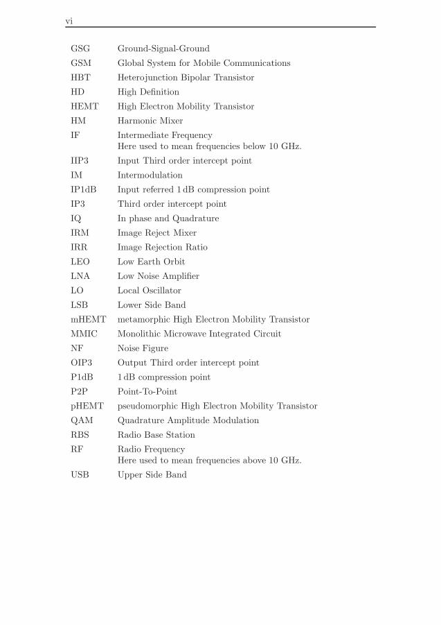
GSG Ground-Signal-Ground
GSM Global System for Mobile Communications
HBT Heterojunction Bipolar Transistor
HD High Definition
HEMT High Electron Mobility Transistor
HM Harmonic Mixer
IF Intermediate FrequencyHere used to mean frequencies below 10 GHz.
IIP3 Input Third order intercept point
IM Intermodulation
IP1dB Input referred 1 dB compression point
IP3 Third order intercept point
IQ In phase and Quadrature
IRM Image Reject Mixer
IRR Image Rejection Ratio
LEO Low Earth Orbit
LNA Low Noise Amplifier
LO Local Oscillator
LSB Lower Side Band
mHEMT metamorphic High Electron Mobility Transistor
MMIC Monolithic Microwave Integrated Circuit
NF Noise Figure
OIP3 Output Third order intercept point
P1dB 1dB compression point
P2P Point-To-Point
pHEMT pseudomorphic High Electron Mobility Transistor
QAM Quadrature Amplitude Modulation
RBS Radio Base Station
RF Radio FrequencyHere used to mean frequencies above 10 GHz.
USB Upper Side Band

vii
Notations
ft Transit frequency
fmax Maximum oscillation frequency
Gbps Gigabit per second
Mbps Megabit per second
Vgs Gate-Source Voltage
Rds Channel Resistance
Cgd Gate-drain capacitance
PLO LO power
PIF IF power
PRF RF power
fLO LO frequency
fIF IF frequency
fRF RF frequency
q Electron charge (Coulomb)

viii

List of Publications
Appended Publications
This thesis is based on work contained in the following papers:
[A] M. Gavell, M. Ferndahl, S. E. Gunnarsson, M. Abbasi, and H. Zirath”An Image Reject Mixer for High-Speed E-band (71-76, 81-86 GHz)Wireless Communication” presented at IEEE Compound SemiconductorIntegrated Circuits Symposium (CSICS) Conference, Greensboro, NC,USA, 2009.
[B] M. Gavell, H. Zirath, M. Ferndahl and S. E. Gunnarsson, ”A linear70-95 GHz di"erential IQ modulator for E-band Wireless Communica-tion,” presented at IEEE International Microwave Symposium (IMS)Conference, Anaheim, CA, USA, 2010.
[C] M. Gavell, M. Ferndahl, S. E. Gunnarsson, H. Zirath, ”A 53 GHz sin-gle chip Receiver for Geostationary Atmospheric Measurements,” pre-sented at IEEE Compound Semiconductor Integrated Circuits Sympo-sium (CSICS) Conference, Kailua Kona, HI, USA, 2011.
ix
x
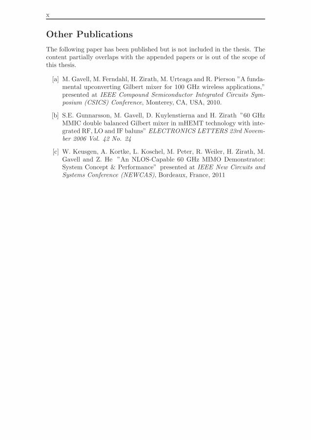
Other Publications
The following paper has been published but is not included in the thesis. Thecontent partially overlaps with the appended papers or is out of the scope ofthis thesis.
[a] M. Gavell, M. Ferndahl, H. Zirath, M. Urteaga and R. Pierson ”A funda-mental upconverting Gilbert mixer for 100 GHz wireless applications,”presented at IEEE Compound Semiconductor Integrated Circuits Sym-posium (CSICS) Conference, Monterey, CA, USA, 2010.
[b] S.E. Gunnarsson, M. Gavell, D. Kuylenstierna and H. Zirath ”60 GHzMMIC double balanced Gilbert mixer in mHEMT technology with inte-grated RF, LO and IF baluns” ELECTRONICS LETTERS 23rd Novem-ber 2006 Vol. 42 No. 24
[c] W. Keusgen, A. Kortke, L. Koschel, M. Peter, R. Weiler, H. Zirath, M.Gavell and Z. He ”An NLOS-Capable 60 GHz MIMO Demonstrator:System Concept & Performance” presented at IEEE New Circuits andSystems Conference (NEWCAS), Bordeaux, France, 2011

Contents
Abstract iii
List of Publications v
Abbreviations and Notations ix
1 Introduction 1
1.1 Motivation . . . . . . . . . . . . . . . . . . . . . . . . . . . . . 11.2 Atmospheric windows . . . . . . . . . . . . . . . . . . . . . . . 21.3 Thesis contribution . . . . . . . . . . . . . . . . . . . . . . . . . 21.4 Thesis outline . . . . . . . . . . . . . . . . . . . . . . . . . . . . 3
2 Mixers for E-band communications 52.1 Microwave backhaul . . . . . . . . . . . . . . . . . . . . . . . . 62.2 Mixer fundamentals . . . . . . . . . . . . . . . . . . . . . . . . 7
2.2.1 Mixer Topologies . . . . . . . . . . . . . . . . . . . . . . 72.2.2 Technology (GaAs mHEMT) . . . . . . . . . . . . . . . 102.2.3 FOM . . . . . . . . . . . . . . . . . . . . . . . . . . . . . 11
2.3 Single balanced IQ modulator . . . . . . . . . . . . . . . . . . . 152.3.1 Design . . . . . . . . . . . . . . . . . . . . . . . . . . . . 152.3.2 Di"erential Branchline Coupler . . . . . . . . . . . . . . 162.3.3 LO suppression . . . . . . . . . . . . . . . . . . . . . . . 182.3.4 Measurement setup and uncertainties . . . . . . . . . . 212.3.5 Results . . . . . . . . . . . . . . . . . . . . . . . . . . . 22
2.4 Image Reject Mixer . . . . . . . . . . . . . . . . . . . . . . . . . 242.4.1 Design . . . . . . . . . . . . . . . . . . . . . . . . . . . . 242.4.2 Results . . . . . . . . . . . . . . . . . . . . . . . . . . . 26
3 53 GHz single chip receiver 29
3.1 Design . . . . . . . . . . . . . . . . . . . . . . . . . . . . . . . . 293.2 Results and comparison . . . . . . . . . . . . . . . . . . . . . . 32
4 Conclusions 35
4.1 Future work . . . . . . . . . . . . . . . . . . . . . . . . . . . . . 36
Acknowledgments 37
Bibliography 39
xi

xii CONTENTS
Chapter 1
Introduction
1.1 Motivation
Applications in high speed communications and remote sensing have foundtheir way into mm-wave frequencies. The atmospheric conditions and licensingpart of the frequency spectrum have attracted these two di"erent applicationsto this frequency range. The development of semiconductor technologies havepushed Monolithic Microwave Integrated Circuit (MMIC) circuit designs toand beyond mm-waves [1]. The High Electron Mobility Transistor (HEMT)is one of possible semiconductor technologies to use in this frequency rangeand it shows excellent performance for MMIC designs. Low noise and linearperformance made this technology the choice for the work presented in thisthesis.
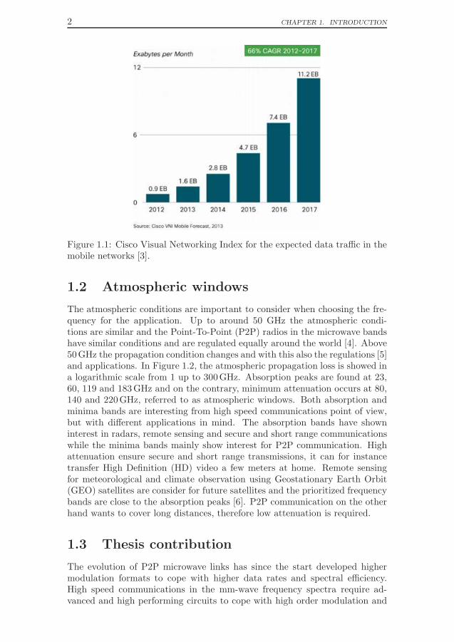
The technology development in the field of electronics has since the dawn ofthe integrated circuit changed our way of living. Wireless communication andflow of information have probably contributed to the biggest change. Mobilevoice service is already considered a necessity by most, and mobile data, video,and TV services are fast becoming an essential part of everybody’s lives. In2009, for the first time in history, the data tra!c was reported to be higherthan voice tra!c and the trend is continuous [2]. The origin of the stan-dardized wireless infrastructure for mobile phones, Global System for MobileCommunications (GSM), is a great achievement over the last decades and haspaved the way for an incredible research and development in the area of elec-tronics for wireless communication. GSM was the first digital cellular system(2G) replacing the analog cellular network (1G). The 2G system was developedover time to handle data tra!c and today, the forth generation standard (4GLTE Advanced) is in use. The expected wireless tra!c contributed over themobile networks is plotted in Figure 1.1 for the coming 5 years. The numberof mobile subscribers is growing rapidly and the demand for bandwidth dueto data and video is increasing fast. Today, microwave backhauls are reportedto be the bottleneck in the wireless networks [3]. To allow mobile broadband,data access, and video services to e"ectively grow and follow consumer usagetrends, the capacity of the microwave backhaul must allow higher data ratesand lower the cost per bit [3].
1
2 CHAPTER 1. INTRODUCTION
Figure 1.1: Cisco Visual Networking Index for the expected data tra!c in themobile networks [3].
1.2 Atmospheric windows
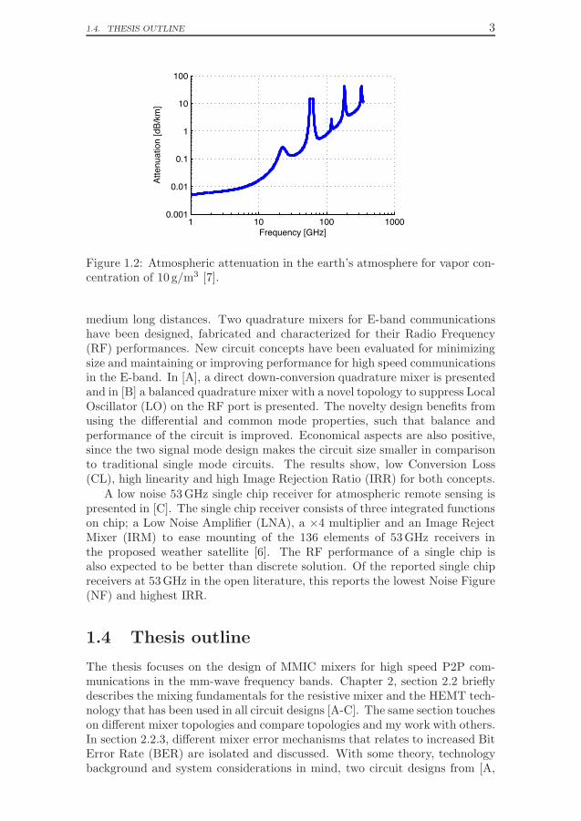
The atmospheric conditions are important to consider when choosing the fre-quency for the application. Up to around 50 GHz the atmospheric condi-tions are similar and the Point-To-Point (P2P) radios in the microwave bandshave similar conditions and are regulated equally around the world [4]. Above50GHz the propagation condition changes and with this also the regulations [5]and applications. In Figure 1.2, the atmospheric propagation loss is showed ina logarithmic scale from 1 up to 300GHz. Absorption peaks are found at 23,60, 119 and 183GHz and on the contrary, minimum attenuation occurs at 80,140 and 220GHz, referred to as atmospheric windows. Both absorption andminima bands are interesting from high speed communications point of view,but with di"erent applications in mind. The absorption bands have showninterest in radars, remote sensing and secure and short range communicationswhile the minima bands mainly show interest for P2P communication. Highattenuation ensure secure and short range transmissions, it can for instancetransfer High Definition (HD) video a few meters at home. Remote sensingfor meteorological and climate observation using Geostationary Earth Orbit(GEO) satellites are consider for future satellites and the prioritized frequencybands are close to the absorption peaks [6]. P2P communication on the otherhand wants to cover long distances, therefore low attenuation is required.
1.3 Thesis contribution
The evolution of P2P microwave links has since the start developed highermodulation formats to cope with higher data rates and spectral e!ciency.High speed communications in the mm-wave frequency spectra require ad-vanced and high performing circuits to cope with high order modulation and
1.4. THESIS OUTLINE 3
1 10 100 10000.001
0.01
0.1
1
10
100
Frequency [GHz]
Atte
nuat
ion
[dB/
km]
Figure 1.2: Atmospheric attenuation in the earth’s atmosphere for vapor con-centration of 10 g/m3 [7].
medium long distances. Two quadrature mixers for E-band communicationshave been designed, fabricated and characterized for their Radio Frequency(RF) performances. New circuit concepts have been evaluated for minimizingsize and maintaining or improving performance for high speed communicationsin the E-band. In [A], a direct down-conversion quadrature mixer is presentedand in [B] a balanced quadrature mixer with a novel topology to suppress LocalOscillator (LO) on the RF port is presented. The novelty design benefits fromusing the di"erential and common mode properties, such that balance andperformance of the circuit is improved. Economical aspects are also positive,since the two signal mode design makes the circuit size smaller in comparisonto traditional single mode circuits. The results show, low Conversion Loss(CL), high linearity and high Image Rejection Ratio (IRR) for both concepts.
A low noise 53GHz single chip receiver for atmospheric remote sensing ispresented in [C]. The single chip receiver consists of three integrated functionson chip; a Low Noise Amplifier (LNA), a !4 multiplier and an Image RejectMixer (IRM) to ease mounting of the 136 elements of 53GHz receivers inthe proposed weather satellite [6]. The RF performance of a single chip isalso expected to be better than discrete solution. Of the reported single chipreceivers at 53GHz in the open literature, this reports the lowest Noise Figure(NF) and highest IRR.
1.4 Thesis outline
The thesis focuses on the design of MMIC mixers for high speed P2P com-munications in the mm-wave frequency bands. Chapter 2, section 2.2 brieflydescribes the mixing fundamentals for the resistive mixer and the HEMT tech-nology that has been used in all circuit designs [A-C]. The same section toucheson di"erent mixer topologies and compare topologies and my work with others.In section 2.2.3, di"erent mixer error mechanisms that relates to increased BitError Rate (BER) are isolated and discussed. With some theory, technologybackground and system considerations in mind, two circuit designs from [A,

4 CHAPTER 1. INTRODUCTION
B] are presented in sections 2.4 and 2.3. In chapter 3, the design and char-acterization of a 53GHz receiver for atmospheric remote sensing is presented[C]. The thesis is concluded in chapter 4 with some final words about futurework.
Chapter 2
Mixers for E-bandcommunications
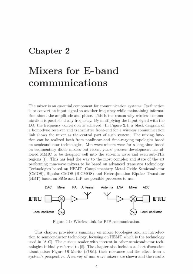
The mixer is an essential component for communication systems. Its functionis to convert an input signal to another frequency while maintaining informa-tion about the amplitude and phase. This is the reason why wireless commu-nication is possible at any frequency. By multiplying the input signal with theLO, the frequency conversion is achieved. In Figure 2.1, a block diagram ofa homodyne receiver and transmitter front-end for a wireless communicationlink shows the mixer as the central part of such system. The mixing func-tion can be realized both from nonlinear and time-varying topologies basedon semiconductor technologies. Mm-wave mixers were for a long time basedon rudimentary diode mixers but recent years’ process development has al-lowed MMIC to be designed well into the sub-mm wave and even sub-THzregions [1]. This has lead the way to the most complex and state of the artperforming mm-wave mixers to be based on advanced transistor technology.Technologies based on HEMT, Complementary Metal Oxide Semiconductor(CMOS), Bipolar CMOS (BiCMOS) and Heterojunction Bipolar Transistor(HBT) based on SiGe and InP are possible processes to use.
Antenna LNA Mixer ADC
Local oscillator
AntennaPAMixerDAC
Local oscillator
Figure 2.1: Wireless link for P2P communication.
This chapter provides a summary on mixer topologies and an introduc-tion to semiconductor technology, focusing on HEMT which is the technologyused in [A-C]. The curious reader with interest in other semiconductor tech-nologies is kindly referred to [8]. The chapter also includes a short discussionabout mixer Figure Of Merits (FOM), their relevance and the e"ect from asystem’s perspective. A survey of mm-wave mixers are shown and the results
5
6 CHAPTER 2. MIXERS FOR E-BAND COMMUNICATIONS
are compared with my work on this topic. Finally, two original mixer designsfor E-band communications will be described and presented.
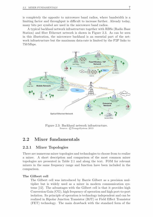
2.1 Microwave backhaul
In the wired world, multi gigabit data transmission has been commerciallyavailable for a long time. Standard protocols such as Gigabit Ethernet (GbE)protocols are sold in millions of commercial devices. Even faster protocols infiber optic networks exists, where 10-GbE, 40-GbE1 and 100-GbE1 are stan-dards for the service of the backbone wired network structures. Using fibershas many positive aspects, they are secure, reliable, provide excellent serviceand speed. However, deploying fibers struggles with installation time, main-tenance, cause disruption and cost which in the end a"ects the users.
For many years now, microwave bands between 6 and 40GHz have beenused for P2P backhauling but the data transmission speed has been far behindfiber optics. The reason for this is simple, the lack of bandwidth. At themicrowave bands, the available channel bandwidth is up to 56MHz, whereasfor fiber several GHz. At the time when the microwave bands were defined,transferring voice was the main purpose and channel bandwidth was relativelynarrow but for transferring data with high speed, wide bandwidth or manysymbols per Hz is necessary. The narrow bands use high order modulation toincrease the spectral e!ciency and o"er more throughput.
The start for licensed wideband P2P communications came in 2003 whenthe Federal Communications Commission (FCC) regulated the E-band for P2Pcommunication. In Figure 2.2, the microwave bands for P2P communicationare illustrated together with the wide band 60GHz and E-band (71-76, 81-86and 92-95GHz). The di"erence in terms of bandwidth between the establishedmicrowave bands and the newer are obvious. Even though the E-band isspecified to three separate bands, the former two are usually referred to as theE-band, and will be so throughout the thesis. Here labeled E1 (70), E2 (80)and E3 (90), shown in Figure 2.2.
E-bandMicrowave bands 60 GHz
10 20 30 40 50 60 70 80 90 100
Frequency [GHz]
E1 E2 E3
Figure 2.2: Illustration of bandwidth in licensed P2P communication links.
Utilizing the available bandwidth at mm-wave, some high speed wirelesstransmission"10Gbps has been reported at 70/80, 120 and 220GHz in [9], [10]and [11] respectively. The high frequency demonstrations use simple modu-lation and high bandwidth to achieve such high data rate transmission. This
1IEEE 802.3ba
2.2. MIXER FUNDAMENTALS 7
is completely the opposite to microwave band radios, where bandwidth is alimiting factor and throughput is di!cult to increase further. Already today,many bits per symbol are used in the microwave band radios.
A typical backhaul network infrastructure together with RBSs (Radio BaseStation) and fiber Ethernet network is shown in Figure 2.3. As can be seenin this illustration, the microwave backhaul is an essential part of the net-work infrastructure but the maximum data-rate is limited by the P2P links to750Mbps.
Figure 2.3: Backhaul network infrastructure.Source: ©TrangoSystem 2013
2.2 Mixer fundamentals
2.2.1 Mixer Topologies
There are numerous mixer topologies and technologies to choose from to realizea mixer. A short description and comparison of the most common mixertopologies are presented in Table 2.1 and along the text. FOM for relevantmixers in the same frequency range and function have been included in thecomparison.
The Gilbert cellThe Gilbert cell was introduced by Barrie Gilbert as a precision mul-tiplier but is widely used as a mixer in modern communication sys-tems [12]. The advantages with the Gilbert cell is that it provides highConversion Gain (CG), high frequency of operation and high port-to-portisolation. Its principle of operation is technology independent and can berealized in Bipolar Junction Transistor (BJT) or Field E"ect Transistor(FET) technology. The main drawback with the standard form of the
8 CHAPTER 2. MIXERS FOR E-BAND COMMUNICATIONS
Gilbert cell is its limited linearity and NF. Due to it’s popularity, sev-eral techniques have been proposed to overcome these issues. In [13], acharge injection method for CMOS technology was suggested to improvethose numbers. Third order intermodulation cancellation or feedforwardtechniques are other techniques that improve linearity [14]. Unfortu-nately, these solutions tend to be frequency or bias sensitive. The iconicBarrie Gilbert published in 1997 “The MICROMIXER” [15], a versionof the classical Gilbert cell replacing the problematic transconductancestage with a bi-symmetrical class-AB input stage to improve linearity.The design of the input stage limits the frequency range but has beenreported as high as 77GHz [16].
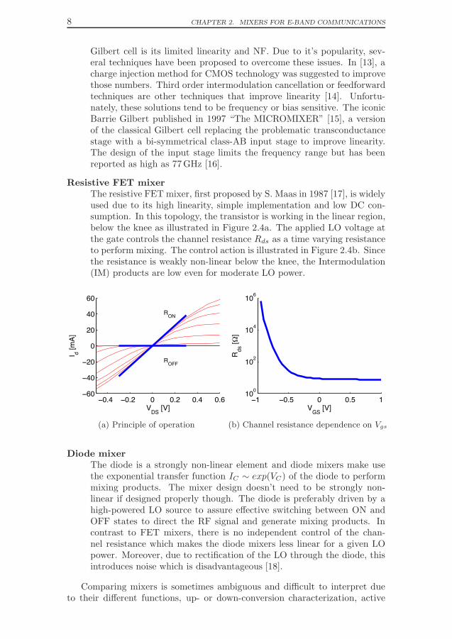
Resistive FET mixerThe resistive FET mixer, first proposed by S. Maas in 1987 [17], is widelyused due to its high linearity, simple implementation and low DC con-sumption. In this topology, the transistor is working in the linear region,below the knee as illustrated in Figure 2.4a. The applied LO voltage atthe gate controls the channel resistance Rds as a time varying resistanceto perform mixing. The control action is illustrated in Figure 2.4b. Sincethe resistance is weakly non-linear below the knee, the Intermodulation(IM) products are low even for moderate LO power.
−0.4 −0.2 0 0.2 0.4 0.6−60
−40
−20
0
20
40
60
RON
ROFF
VDS [V]
I d [mA]
(a) Principle of operation
−1 −0.5 0 0.5 1100
102
104
106
VGS [V]
R ds [Ω
]
(b) Channel resistance dependence on Vgs
Diode mixerThe diode is a strongly non-linear element and diode mixers make usethe exponential transfer function IC # exp(VC) of the diode to performmixing products. The mixer design doesn’t need to be strongly non-linear if designed properly though. The diode is preferably driven by ahigh-powered LO source to assure e"ective switching between ON andOFF states to direct the RF signal and generate mixing products. Incontrast to FET mixers, there is no independent control of the chan-nel resistance which makes the diode mixers less linear for a given LOpower. Moreover, due to rectification of the LO through the diode, thisintroduces noise which is disadvantageous [18].
Comparing mixers is sometimes ambiguous and di!cult to interpret dueto their di"erent functions, up- or down-conversion characterization, active
2.2. MIXER FUNDAMENTALS 9
output bu"er amplifiers etc. Luckily, common parameters for mixers existsand are included in the comparison in Table 2.1.
In terms of linearity (1 dB compression point (P1dB) and Third order in-tercept point (IP3)), the resistive mixers report among the highest results,including my work. The Output IP3 (OIP3) in [B] shows 13 dBm and OutputP1dB (OP1dB) during 2-tone measurement of 0 dBm. The OIP3 is far bet-ter than [19] and [16] but lower OP1dB than [16] and [20]. In [21], a bu"eramplifier is included which disqualifies it in the comparison.
Active mixers such as the Gilbert cell, has the characteristic of achievingpositive CG, but this feature does not necessarily need to be advantageous.For instance, increased CG will reduce the Input IP3 (IIP3) of the mixer,which might be disadvantageous. Nevertheless, all active mixers show higherCG than the passive mixers.
NF is only reported in two of the references, the micromixer and a diodemixer [16] and [22] respectively. In this duel, the diode mixer is a clear winner,the others can only be speculated or referred to theory. In theory though, theFET technology has an advantage over BJT and HBT technology in termsof noise. HBTs and BJTs introduce shot-noise since they always need basecurrent Ib to operate, something FETs simply are free from. Therefore, theNF of a FET is normally lower to that of a BJT. In the case of the resistivemixer, the generated noise is purely thermal, therefore the NF is comparableto the CL. FETs also have a slight edge in added noise compared to diodesdue to the rectification of LO current.
The topologies seem not to have any large influence on the function. For thereported IRR and LO-RF isolation, most show similar number which indicatesthat the topology doesn’t a"ect the function.
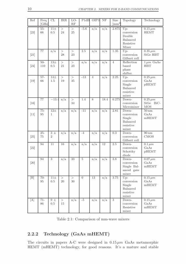
10 CHAPTER 2. MIXERS FOR E-BAND COMMUNICATIONS
Ref Freq[GHz]
CL IRR LO-RF
P1dB OIP3 NF Size[mm2]
Topology Technology
[23]55-66
11±0.5
>
24>
25-5.6 n/a n/a 2.875 Up-
conversionDoubleBalancedResistiveMixer
0.15 µmHEMT
[21]77 n/a >
28>
232.5 n/a n/a 1.35 Up-
conversionGilbert cell
0.35 µmSiGe HBT
[24]50-110
13±0.5
>
21>
23n/a n/a n/a 4 Reflection
basedphaseshifter
1 µm GaAsHBT
[19]57-66
14±1.5
>
19>
35-13 4 n/a 2.25 Up-
conversionSingleBalancedresistivemixer
0.25 µmGaAspHEMT
[16]77 !13.4 n/a >
341.4 8 18.4 0.275 Down-
conversionMicromixer
0.25 µmSiGe BiC-MOS
[11]75-95
12±1
n/a n/a -11 n/a n/a 2.81 Down-conversionSingleBalancedresistivemixer
50 nmGaAsmHEMT
[25]25-75
3 ±
2n/a n/a -4 n/a n/a 0.3 Down-
conversionGilbert cell
90 nmCMOS
[22]94 11 16 n/a n/a n/a 12 2.5 Down-
conversionSchottkydiode
0.1µmGaAspHEMT
[20]94 3 n/a 33 5 n/a n/a 3.8 Down-
conversionSingle Bal-anced gatemixer
0.07 µmGaAsmHEMT
[B] 70-95
11±0.5
>
20>
300 13 n/a 3.75 Up-
conversionSingleBalancedresistivemixer
0.15 µmGaAsmHEMT
[A] 71-86
9 ±
0.5>
15n/a -5 n/a n/a 3 Down-
conversionResistivemixer
0.15 µmGaAsmHEMT
Table 2.1: Comparison of mm-wave mixers
2.2.2 Technology (GaAs mHEMT)
The circuits in papers A-C were designed in 0.15µm GaAs metamorphicHEMT (mHEMT) technology, for good reasons. It’s a mature and stable
2.2. MIXER FUNDAMENTALS 11
technology and provides overall good high frequency performance. The maindrawback with GaAs HEMT technology is the chip area, mainly due to theless advanced Back End of Line (BEOL) but to some extent to the highercurrent density in HBTs and CMOS which makes the physical size of thosetransistors smaller. All Gilbert cell based mixers in SiGe HBT, BiCMOS orCMOS are considerably smaller in size, around 1:10 of the circuits included inthe comparison in Table 2.1.
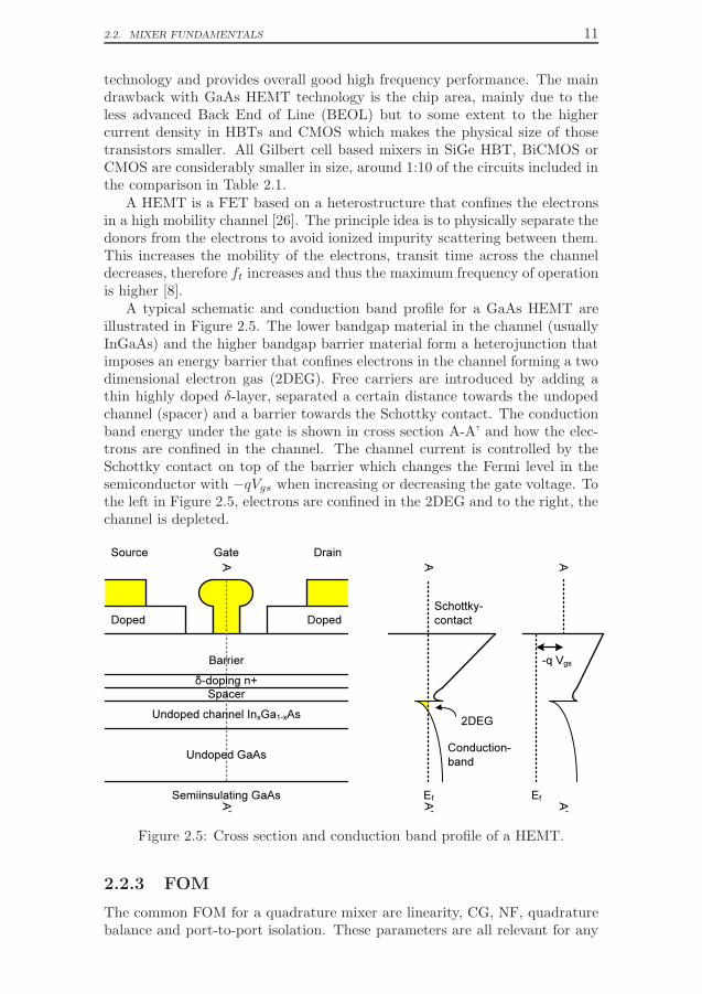
A HEMT is a FET based on a heterostructure that confines the electronsin a high mobility channel [26]. The principle idea is to physically separate thedonors from the electrons to avoid ionized impurity scattering between them.This increases the mobility of the electrons, transit time across the channeldecreases, therefore ft increases and thus the maximum frequency of operationis higher [8].
A typical schematic and conduction band profile for a GaAs HEMT areillustrated in Figure 2.5. The lower bandgap material in the channel (usuallyInGaAs) and the higher bandgap barrier material form a heterojunction thatimposes an energy barrier that confines electrons in the channel forming a twodimensional electron gas (2DEG). Free carriers are introduced by adding athin highly doped !-layer, separated a certain distance towards the undopedchannel (spacer) and a barrier towards the Schottky contact. The conductionband energy under the gate is shown in cross section A-A’ and how the elec-trons are confined in the channel. The channel current is controlled by theSchottky contact on top of the barrier which changes the Fermi level in thesemiconductor with $qVgs when increasing or decreasing the gate voltage. Tothe left in Figure 2.5, electrons are confined in the 2DEG and to the right, thechannel is depleted.
Source Gate Drain
DopedDoped
Undoped channel InxGa1-xAs
Undoped GaAs
Semiinsulating GaAs
Schottky-
contact
Conduction-
band
Ef
-q Vgs
Ef
Spacer
!-doping n+
Barrier
AA’
2DEG
AA’
AA’
Figure 2.5: Cross section and conduction band profile of a HEMT.
2.2.3 FOM
The common FOM for a quadrature mixer are linearity, CG, NF, quadraturebalance and port-to-port isolation. These parameters are all relevant for any
12 CHAPTER 2. MIXERS FOR E-BAND COMMUNICATIONS
mixer but depending on the application, some are more important than others.In digital communications, low BER, high dynamic range and high throughputare characteristics for a wireless link’s performance. The maximum throughputof a link is the available RF bandwidth ! number of bits per symbols and theupper bound for symbol e!ciency (Nyquist rate, bits per Hz) is given byN = log2 (M). M is the number of symbols and N then the symbol e!ciencyin bits per symbol. Quadrature Amplitude Modulation (QAM) is one of themost common and spectral e!cient modulation formats that is flexible tothese characteristics of a receiver. These characteristics include accuracy ofthe amplitude, phase, and frequency of each baseband signal. For simplemodulation schemes such as 4-QAM or Binary Phase Shift Keying (BPSK),relatively inaccurate baseband signals are tolerable but the symbol e!ciencyis lower. However, for higher order modulation schemes such as 64-QAMand 256-QAM, baseband accuracy is essential. For these modulation schemes,small errors of DC o"set, phase noise, quadrature skew, or IQ gain imbalancecan make the transitions of the RF signal too di!cult to distinguish.
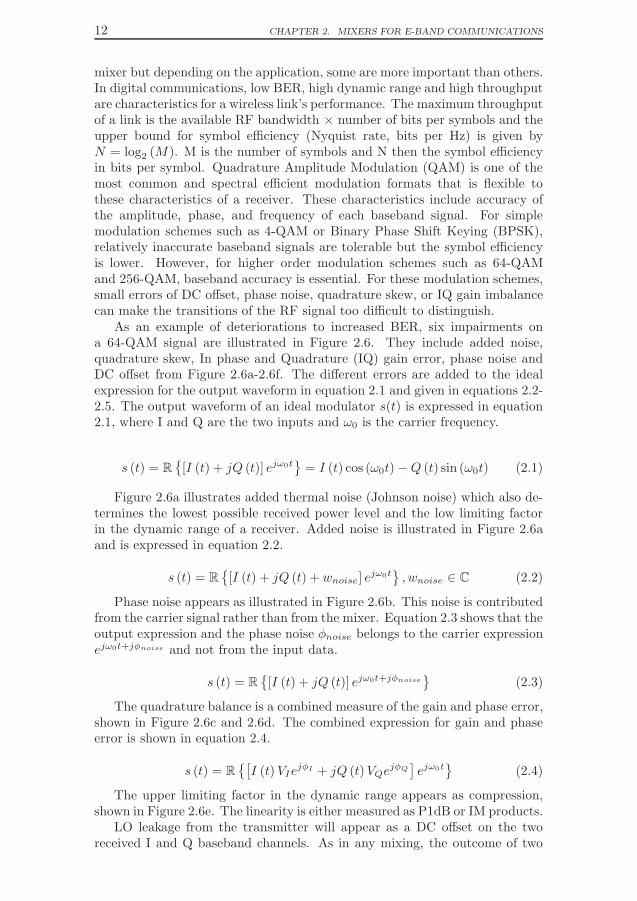
As an example of deteriorations to increased BER, six impairments ona 64-QAM signal are illustrated in Figure 2.6. They include added noise,quadrature skew, In phase and Quadrature (IQ) gain error, phase noise andDC o"set from Figure 2.6a-2.6f. The di"erent errors are added to the idealexpression for the output waveform in equation 2.1 and given in equations 2.2-2.5. The output waveform of an ideal modulator s(t) is expressed in equation2.1, where I and Q are the two inputs and "0 is the carrier frequency.
s (t) = R!
[I (t) + jQ (t)] ej!0t"
= I (t) cos ("0t)$Q (t) sin ("0t) (2.1)
Figure 2.6a illustrates added thermal noise (Johnson noise) which also de-termines the lowest possible received power level and the low limiting factorin the dynamic range of a receiver. Added noise is illustrated in Figure 2.6aand is expressed in equation 2.2.
s (t) = R!
[I (t) + jQ (t) + wnoise] ej!0t
"
, wnoise % C (2.2)
Phase noise appears as illustrated in Figure 2.6b. This noise is contributedfrom the carrier signal rather than from the mixer. Equation 2.3 shows that theoutput expression and the phase noise #noise belongs to the carrier expressionej!0t+j"noise and not from the input data.
s (t) = R!
[I (t) + jQ (t)] ej!0t+j"noise"
(2.3)
The quadrature balance is a combined measure of the gain and phase error,shown in Figure 2.6c and 2.6d. The combined expression for gain and phaseerror is shown in equation 2.4.
s (t) = R!#
I (t) VIej"I + jQ (t)VQe
j"Q$
ej!0t"
(2.4)
The upper limiting factor in the dynamic range appears as compression,shown in Figure 2.6e. The linearity is either measured as P1dB or IM products.
LO leakage from the transmitter will appear as a DC o"set on the tworeceived I and Q baseband channels. As in any mixing, the outcome of two

2.2. MIXER FUNDAMENTALS 13
identical signals will be fLO ± fLO, thus a DC level plus a 2fLO component.The 2fLO product can simply be filtered but the DC component might beproblematic unless AC coupled pattern is used. Equal DC o"set on the twochannels is illustrated in Figure 2.6f and equation 2.5. A large LO leakage onthe transmitter will be amplified in the band and a"ect the performance of thetransmitter, leading to lower output power and IP3 of the converted signal.
s (t) = R!
[I (t) + IDC + j (Q (t) +QDC)] ej!0t
"
(2.5)

14 CHAPTER 2. MIXERS FOR E-BAND COMMUNICATIONS
−1.5 −1 −0.5 0 0.5 1 1.5−1.5
−1
−0.5
0
0.5
1
1.5
I
Q
(a) Johnson noise, Temperature noise
−1.5 −1 −0.5 0 0.5 1 1.5−1.5
−1
−0.5
0
0.5
1
1.5
IQ
(b) Phase noise
−1.5 −1 −0.5 0 0.5 1 1.5−1.5
−1
−0.5
0
0.5
1
1.5
I
Q
(c) IQ phase noise
−1.5 −1 −0.5 0 0.5 1 1.5−1.5
−1
−0.5
0
0.5
1
1.5
I
Q
(d) IQ gain error
−1.5 −1 −0.5 0 0.5 1 1.5−1.5
−1
−0.5
0
0.5
1
1.5
I
Q
(e) IF compression
−1.5 −1 −0.5 0 0.5 1 1.5−1.5
−1
−0.5
0
0.5
1
1.5
I
Q
(f) DC o!set
Figure 2.6: Typical impairments on a 64 QAM constellation
2.3. SINGLE BALANCED IQ MODULATOR 15
2.3 Single balanced IQ modulator
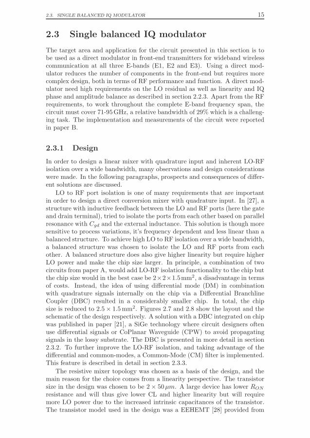
The target area and application for the circuit presented in this section is tobe used as a direct modulator in front-end transmitters for wideband wirelesscommunication at all three E-bands (E1, E2 and E3). Using a direct mod-ulator reduces the number of components in the front-end but requires morecomplex design, both in terms of RF performance and function. A direct mod-ulator need high requirements on the LO residual as well as linearity and IQphase and amplitude balance as described in section 2.2.3. Apart from the RFrequirements, to work throughout the complete E-band frequency span, thecircuit must cover 71-95GHz, a relative bandwidth of 29% which is a challeng-ing task. The implementation and measurements of the circuit were reportedin paper B.
2.3.1 Design
In order to design a linear mixer with quadrature input and inherent LO-RFisolation over a wide bandwidth, many observations and design considerationswere made. In the following paragraphs, prospects and consequences of di"er-ent solutions are discussed.
LO to RF port isolation is one of many requirements that are importantin order to design a direct conversion mixer with quadrature input. In [27], astructure with inductive feedback between the LO and RF ports (here the gateand drain terminal), tried to isolate the ports from each other based on parallelresonance with Cgd and the external inductance. This solution is though moresensitive to process variations, it’s frequency dependent and less linear than abalanced structure. To achieve high LO to RF isolation over a wide bandwidth,a balanced structure was chosen to isolate the LO and RF ports from eachother. A balanced structure does also give higher linearity but require higherLO power and make the chip size larger. In principle, a combination of twocircuits from paper A, would add LO-RF isolation functionality to the chip butthe chip size would in the best case be 2!2!1.5mm2, a disadvantage in termsof costs. Instead, the idea of using di"erential mode (DM) in combinationwith quadrature signals internally on the chip via a Di"erential BranchlineCoupler (DBC) resulted in a considerably smaller chip. In total, the chipsize is reduced to 2.5! 1.5mm2. Figures 2.7 and 2.8 show the layout and theschematic of the design respectively. A solution with a DBC integrated on chipwas published in paper [21], a SiGe technology where circuit designers oftenuse di"erential signals or CoPlanar Waveguide (CPW) to avoid propagatingsignals in the lossy substrate. The DBC is presented in more detail in section2.3.2. To further improve the LO-RF isolation, and taking advantage of thedi"erential and common-modes, a Common-Mode (CM) filter is implemented.This feature is described in detail in section 2.3.3.
The resistive mixer topology was chosen as a basis of the design, and themain reason for the choice comes from a linearity perspective. The transistorsize in the design was chosen to be 2! 50µm. A large device has lower RON
resistance and will thus give lower CL and higher linearity but will requiremore LO power due to the increased intrinsic capacitances of the transistor.The transistor model used in the design was a EEHEMT [28] provided from
16 CHAPTER 2. MIXERS FOR E-BAND COMMUNICATIONS
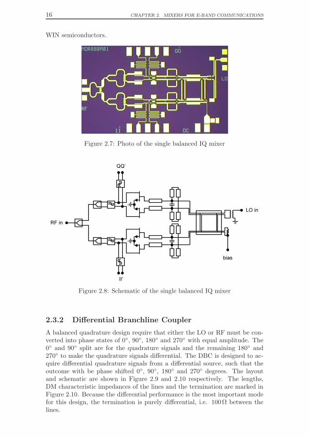
WIN semiconductors.
Figure 2.7: Photo of the single balanced IQ mixer
RF in
LO in
QQ’
II’
bias
Figure 2.8: Schematic of the single balanced IQ mixer
2.3.2 Di!erential Branchline Coupler
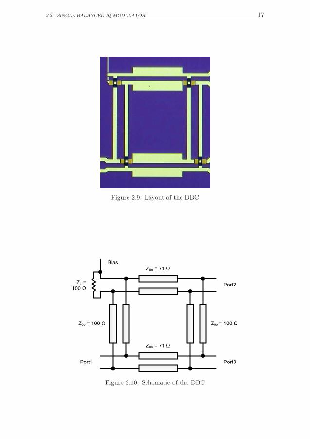
A balanced quadrature design require that either the LO or RF must be con-verted into phase states of 0!, 90!, 180! and 270! with equal amplitude. The0! and 90! split are for the quadrature signals and the remaining 180! and270! to make the quadrature signals di"erential. The DBC is designed to ac-quire di"erential quadrature signals from a di"erential source, such that theoutcome with be phase shifted 0!, 90!, 180! and 270! degrees. The layoutand schematic are shown in Figure 2.9 and 2.10 respectively. The lengths,DM characteristic impedances of the lines and the termination are marked inFigure 2.10. Because the di"erential performance is the most important modefor this design, the termination is purely di"erential, i.e. 100# between thelines.
2.3. SINGLE BALANCED IQ MODULATOR 17
Figure 2.9: Layout of the DBC
ZL
=
100 !
Z0o
= 71 !
Z0o
= 100 !
Z0o
= 71 !
Z0o
= 100 !
Port1 Port3
Port2
Bias
Figure 2.10: Schematic of the DBC
18 CHAPTER 2. MIXERS FOR E-BAND COMMUNICATIONS
+ -
(a) Di!erential mode
+ +
(b) Common mode
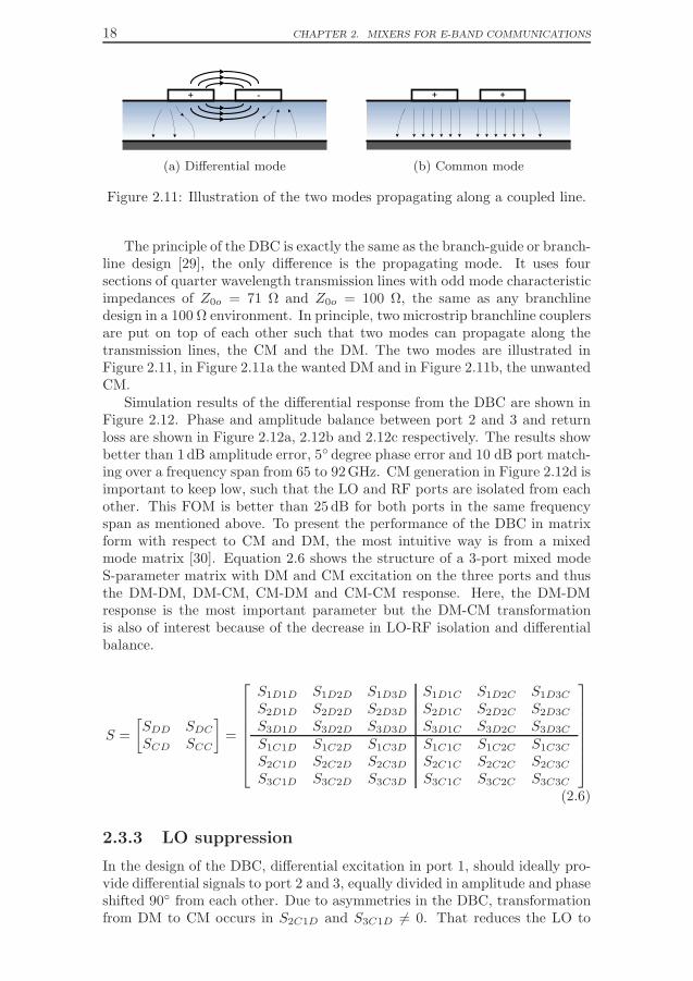
Figure 2.11: Illustration of the two modes propagating along a coupled line.
The principle of the DBC is exactly the same as the branch-guide or branch-line design [29], the only di"erence is the propagating mode. It uses foursections of quarter wavelength transmission lines with odd mode characteristicimpedances of Z0o = 71 # and Z0o = 100 #, the same as any branchlinedesign in a 100 # environment. In principle, two microstrip branchline couplersare put on top of each other such that two modes can propagate along thetransmission lines, the CM and the DM. The two modes are illustrated inFigure 2.11, in Figure 2.11a the wanted DM and in Figure 2.11b, the unwantedCM.
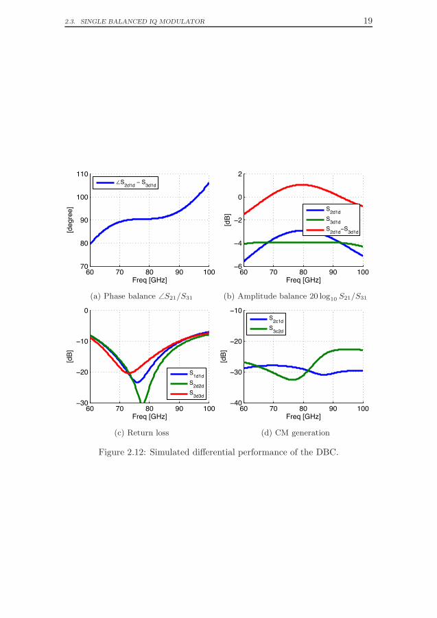
Simulation results of the di"erential response from the DBC are shown inFigure 2.12. Phase and amplitude balance between port 2 and 3 and returnloss are shown in Figure 2.12a, 2.12b and 2.12c respectively. The results showbetter than 1 dB amplitude error, 5! degree phase error and 10 dB port match-ing over a frequency span from 65 to 92GHz. CM generation in Figure 2.12d isimportant to keep low, such that the LO and RF ports are isolated from eachother. This FOM is better than 25 dB for both ports in the same frequencyspan as mentioned above. To present the performance of the DBC in matrixform with respect to CM and DM, the most intuitive way is from a mixedmode matrix [30]. Equation 2.6 shows the structure of a 3-port mixed modeS-parameter matrix with DM and CM excitation on the three ports and thusthe DM-DM, DM-CM, CM-DM and CM-CM response. Here, the DM-DMresponse is the most important parameter but the DM-CM transformationis also of interest because of the decrease in LO-RF isolation and di"erentialbalance.
S =
%
SDD SDC
SCD SCC
&
=
'
(
(
(
(
(
(
)
S1D1D S1D2D S1D3D S1D1C S1D2C S1D3C
S2D1D S2D2D S2D3D S2D1C S2D2C S2D3C
S3D1D S3D2D S3D3D S3D1C S3D2C S3D3C
S1C1D S1C2D S1C3D S1C1C S1C2C S1C3C
S2C1D S2C2D S2C3D S2C1C S2C2C S2C3C
S3C1D S3C2D S3C3D S3C1C S3C2C S3C3C
*
+
+
+
+
+
+
,
(2.6)
2.3.3 LO suppression
In the design of the DBC, di"erential excitation in port 1, should ideally pro-vide di"erential signals to port 2 and 3, equally divided in amplitude and phaseshifted 90! from each other. Due to asymmetries in the DBC, transformationfrom DM to CM occurs in S2C1D and S3C1D &= 0. That reduces the LO to
2.3. SINGLE BALANCED IQ MODULATOR 19
60 70 80 90 10070
80
90
100
110
Freq [GHz]
[deg
ree]
∠S2d1d − S3d1d
(a) Phase balance !S21/S31
60 70 80 90 100−6
−4
−2
0
2
Freq [GHz]
[dB]
S2d1dS3d1dS2d1d−S3d1d
(b) Amplitude balance 20 log10 S21/S31
60 70 80 90 100−30
−20
−10
0
Freq [GHz]
[dB]
S1d1dS2d2dS3d3d
(c) Return loss
60 70 80 90 100−40
−30
−20
−10
Freq [GHz]
[dB]
S2c1dS3c2d
(d) CM generation
Figure 2.12: Simulated di"erential performance of the DBC.
20 CHAPTER 2. MIXERS FOR E-BAND COMMUNICATIONS
Port1 Port2
!/4
!/4
(a) Schematic
(b) Layout
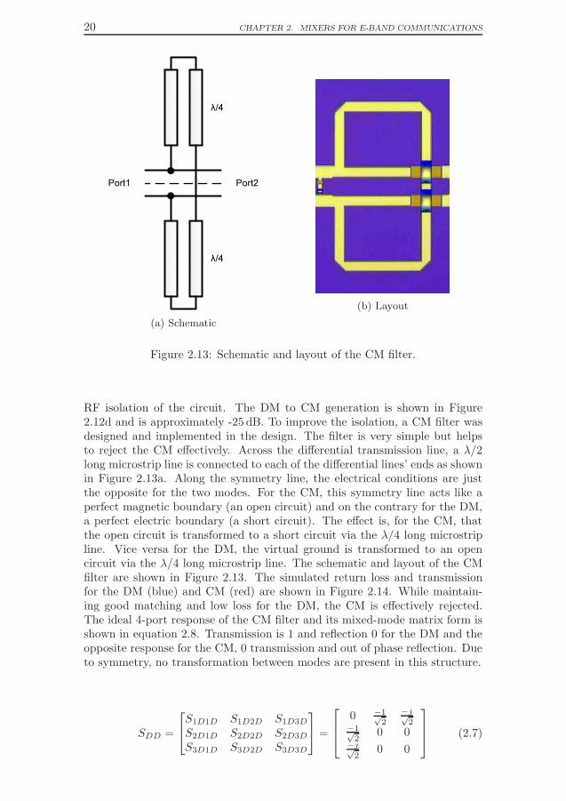
Figure 2.13: Schematic and layout of the CM filter.
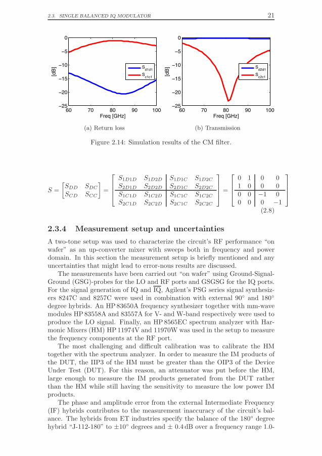
RF isolation of the circuit. The DM to CM generation is shown in Figure2.12d and is approximately -25 dB. To improve the isolation, a CM filter wasdesigned and implemented in the design. The filter is very simple but helpsto reject the CM e"ectively. Across the di"erential transmission line, a $/2long microstrip line is connected to each of the di"erential lines’ ends as shownin Figure 2.13a. Along the symmetry line, the electrical conditions are justthe opposite for the two modes. For the CM, this symmetry line acts like aperfect magnetic boundary (an open circuit) and on the contrary for the DM,a perfect electric boundary (a short circuit). The e"ect is, for the CM, thatthe open circuit is transformed to a short circuit via the $/4 long microstripline. Vice versa for the DM, the virtual ground is transformed to an opencircuit via the $/4 long microstrip line. The schematic and layout of the CMfilter are shown in Figure 2.13. The simulated return loss and transmissionfor the DM (blue) and CM (red) are shown in Figure 2.14. While maintain-ing good matching and low loss for the DM, the CM is e"ectively rejected.The ideal 4-port response of the CM filter and its mixed-mode matrix form isshown in equation 2.8. Transmission is 1 and reflection 0 for the DM and theopposite response for the CM, 0 transmission and out of phase reflection. Dueto symmetry, no transformation between modes are present in this structure.
SDD =
'
)
S1D1D S1D2D S1D3D
S2D1D S2D2D S2D3D
S3D1D S3D2D S3D3D
*
, =
'
(
)
0 "1#2
"j#2
"1#2
0 0"j#2
0 0
*
+
,(2.7)
2.3. SINGLE BALANCED IQ MODULATOR 21
60 70 80 90 100−25
−20
−15
−10
−5
0
Freq [GHz]
[dB]
Sd1d1Sc1c1
(a) Return loss
60 70 80 90 100−25
−20
−15
−10
−5
0
Freq [GHz]
[dB]
Sd2d1Sc2c1
(b) Transmission
Figure 2.14: Simulation results of the CM filter.
S =
%
SDD SDC
SCD SCC
&
=
'
(
(
)
S1D1D S1D2D S1D1C S1D2C
S2D1D S2D2D S2D1C S2D2C
S1C1D S1C2D S1C1C S1C2C
S2C1D S2C2D S2C1C S2C2C
*
+
+
,
=
'
(
(
)
0 1 0 01 0 0 00 0 $1 00 0 0 $1
*
+
+
,
(2.8)
2.3.4 Measurement setup and uncertainties
A two-tone setup was used to characterize the circuit’s RF performance “onwafer” as an up-converter mixer with sweeps both in frequency and powerdomain. In this section the measurement setup is briefly mentioned and anyuncertainties that might lead to error-nous results are discussed.
The measurements have been carried out “on wafer” using Ground-Signal-Ground (GSG)-probes for the LO and RF ports and GSGSG for the IQ ports.For the signal generation of IQ and IQ, Agilent’s PSG series signal synthesiz-ers 8247C and 8257C were used in combination with external 90! and 180!
degree hybrids. An HP83650A frequency synthesizer together with mm-wavemodules HP83558A and 83557A for V- and W-band respectively were used toproduce the LO signal. Finally, an HP8565EC spectrum analyzer with Har-monic Mixers (HM) HP11974V and 11970W was used in the setup to measurethe frequency components at the RF port.
The most challenging and di!cult calibration was to calibrate the HMtogether with the spectrum analyzer. In order to measure the IM products ofthe DUT, the IIP3 of the HM must be greater than the OIP3 of the DeviceUnder Test (DUT). For this reason, an attenuator was put before the HM,large enough to measure the IM products generated from the DUT ratherthan the HM while still having the sensitivity to measure the low power IMproducts.
The phase and amplitude error from the external Intermediate Frequency(IF) hybrids contributes to the measurement inaccuracy of the circuit’s bal-ance. The hybrids from ET industries specify the balance of the 180! degreehybrid “J-112-180” to ±10! degrees and ± 0.4 dB over a frequency range 1.0-

22 CHAPTER 2. MIXERS FOR E-BAND COMMUNICATIONS
12.4GHz and the 90! degree hybrid “Q-112-90” to ±6! degrees and ± 0.4 dBover a frequency range 1.0-12.4GHz. The largest inaccuracy from the mea-surement results are related to the external hybrids and the IRR. 20 dB IRRtranslates to a maximum phase imbalance of 11.5 ! degrees or a maximum am-plitude imbalance of 1.75dB. For this reason, due to the large uncertainty ofthe phase error of the hybrids, the accuracy of IRR is limited.
2.3.5 Results
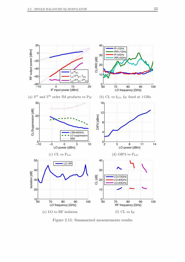
The measurements were carried out with Continuous Waveform (CW) signalsas described in section 2.3.4. The results from the measurements are summa-rized in Figure 2.15.
Figure 2.15a shows how the converted signal and the third and fifth IMproducts vary versus IF power. The extrapolated OIP3 occurs at a maximumof 13 dBm with an LO input power level of 13 dBm. Even at input IF powerlevels of 0 dBm, the IM suppression is more than 40 dBc.
While sweeping the LO power in Figure 2.15d and 2.15c, the response fromOIP3, CL, IRR and LO-RF separation is shown. OIP3 shows a linear behaviorwith respect to the LO power in the range from 2 dBm to 13dBm, where italso peaks at maximum 13dBm. CL and IRR also improves with increasedLO power, which is expected. The IRR is improved because the amplitudevariation in the DBC becomes less important, due to the CL saturation. Insummary, everything except RF-LO separation is benefited from a high LOdrive.
In Figure 2.15b and 2.15e the LO frequency has been swept for seeing theLO bandwidth response. The CL is smooth around 11 dB and the IRR mea-sures more than 20 dB over the E1-E3 frequency range. Taking into accountthe error contributions from the IF hybrids, the IRR on the circuit is mostprobably better than the measurement shows. Also the LO-RF isolation inFigure 2.15e is measured higher than 30 dB over all three E-bands.
In Figure 2.15f, the LO is fixed in the center of the three E-band frequencywindows while sweeping the IF from -2 to 2GHz. When the IF is negative, theside-band is measured on the Upper Side Band (USB) and RF on the LowerSide Band (LSB). When positive, the side-band is measured on the LSB sideand RF on the USB, therefore the RF and sideband are on top of each other.This tell, that the high IRR and CL remain over large IF bandwidths in allthree E-bands.
The results are overall very satisfying for a new concept topology whichtakes advantage of the CM and DM properties and make the design morecompact. High linearity, high IRR and compactness over wide bandwidth makethis circuit very suitable for communications in the E1, E2 and E3 frequencybands.
2.3. SINGLE BALANCED IQ MODULATOR 23
−10 0 10 20−80
−60
−40
−20
0
20
IF input power [dBm]
RF o
utpu
t pow
er [d
Bm]
fLO+fIF1fLO+2*fIF1−fIF2fLO+3*fIF1−2*fIF1
(a) 3rd and 5th order IM products vs PIF
60 70 80 90 1000
10
20
30
40
LO frequency [GHz]
CL/IR
R [d
B]
IF=1GHzIRR=1GHzIF=5GHzIRR=5GHz
(b) CL vs fLO, fIF fixed at 1GHz
−10 −5 0 5 100
10
20
30
LO power [dBm]
CL/S
uppr
essio
n [d
B]
LSB=85GHzLO suppressionSBS
(c) CL vs PLO
2 5 8 11 140
4
8
12
16
LO power [dBm]
OIP
3 [d
Bm]
(d) OIP3 vs PLO
60 70 80 90 10010
20
30
40
50
LO frequency [GHz]
Isol
atio
n [d
B]
LO−RF
(e) LO to RF isolation
60 70 80 90 1000
10
20
30
40
RF frequency [GHz]
CL [d
B]
LO=73GHzLO=83GHzLO=93GHz
(f) CL vs fIF
Figure 2.15: Summarized measurements results
24 CHAPTER 2. MIXERS FOR E-BAND COMMUNICATIONS
2.4 Image Reject Mixer
The IRM presented in [A] is an example of a classic resistive IRM. The choicefor designing a quadrature mixer comes from the expectations of using QAMmodulated signals for P2P communication in the E-band. In section 2.3, thedesign of an up-converting IQ mixer was presented, and in this section thedesign and design-considerations of a down-conversion mixer is presented. Ina receiver mixer, the requirements are similar to a transmitter mixer, with thedi"erence that NF is more important and the LO-RF isolation is no longer astrong requirement. Without the need of a balanced structure, the circuit canbe designed smaller and use more e"ectively lower LO power. The quadratureE-band mixer was reported in [A].
2.4.1 Design
In a communication receiver, linearity and NF are the two most importantFOM to consider for high dynamic range. The comparison made in section2.2.3 concludes that HEMT technology provides lower NF due to the absenceof shot-noise and that the Gilbert cell is di!cult to implement in a low levelintegration process. In terms of noise, the Schottky diode based design [22]achieves the lowest NF in the comparison, but requires high LO power whichusually is the drawback of diode based mixers. For these combined reasons,the resistive mixer topology is again chosen as the basis topology.
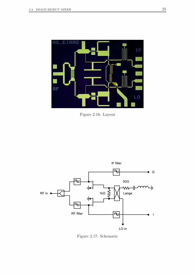
The design of this down-converting quadrature mixer for E-band commu-nications consists of two mixer cells, a 90! degree phase shifter, IF filters and apower combiner. Layout and schematic of the circuit are shown in Figure 2.16and 2.17 respectively. In comparison to the single balanced mixer presentedin section 2.3, this mixer provides quadrature signals but lacks features suchas a balanced topology to isolate the LO and RF ports from each other. Ina receiver, the reverse isolation (S12) of the LNA e"ectively isolates the LOsignal from the RF port, therefore it’s usually unnecessary to add this functionto the mixer. The main advantage with reduced requirements is a simpler de-sign, more compact and requires lower LO power. The total chip size measures2.0! 1.5mm2, which is 0.75mm2 smaller than the single balanced mixer.
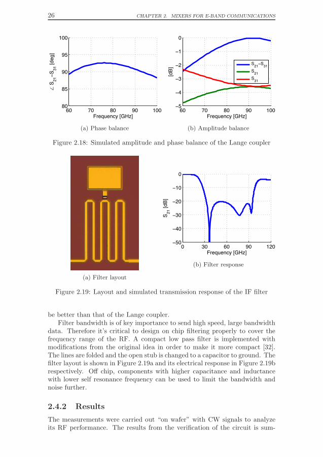
To provide quadrature signals, this design uses a Lange coupler [31] for the90! degree phase shift instead of the branchline coupler. One of the attrac-tions with the Lange coupler is its wide bandwidth and compact layout. InFigure 2.18, the simulated amplitude and phase balance of the Lange coupleris ±2! degree and ±1dB. In comparison to the simulated phase balance of theDBC in Figure 2.12, the response is ±2! degree to ±10! degree over the samefrequency range, a considerably larger bandwidth. The amplitude balance is±2dB and ±1 dB in favor to the DBC. The Lange coupler is fed to the gatesof the mixer for more reasons than providing quadrature signals. First, thegates of FETs are in general di!cult to match to 50# over a wide bandwidthdue to the capacitive input network and high transformation ratio. Therefore,the Lange coupler on the LO will provide excellent match to this otherwisedi!cult port to match. Second, amplitude imbalance of the Lange coupler isless important due to CL saturation with LO power. Figure 2.20c illustrateshow the CL saturates with LO power, therefore the IQ amplitude balance can
2.4. IMAGE REJECT MIXER 25
Figure 2.16: Layout
RF in
LO in
Q
IRF filter
IF filter
1k!
50!
Lange
Figure 2.17: Schematic
26 CHAPTER 2. MIXERS FOR E-BAND COMMUNICATIONS
60 70 80 90 10080
85
90
95
100
Frequency [GHz]
∠ S
21−S
31 [d
eg]
(a) Phase balance
60 70 80 90 100−5
−4
−3
−2
−1
0
Frequency [GHz]
[dB]
S21−S31S21S31
(b) Amplitude balance
Figure 2.18: Simulated amplitude and phase balance of the Lange coupler
(a) Filter layout
0 30 60 90 120−50
−40
−30
−20
−10
0
Frequency [GHz]
S 21 [d
B]
(b) Filter response
Figure 2.19: Layout and simulated transmission response of the IF filter
be better than that of the Lange coupler.Filter bandwidth is of key importance to send high speed, large bandwidth
data. Therefore it’s critical to design on chip filtering properly to cover thefrequency range of the RF. A compact low pass filter is implemented withmodifications from the original idea in order to make it more compact [32].The lines are folded and the open stub is changed to a capacitor to ground. Thefilter layout is shown in Figure 2.19a and its electrical response in Figure 2.19brespectively. O" chip, components with higher capacitance and inductancewith lower self resonance frequency can be used to limit the bandwidth andnoise further.
2.4.2 Results
The measurements were carried out “on wafer” with CW signals to analyzeits RF performance. The results from the verification of the circuit is sum-
2.4. IMAGE REJECT MIXER 27
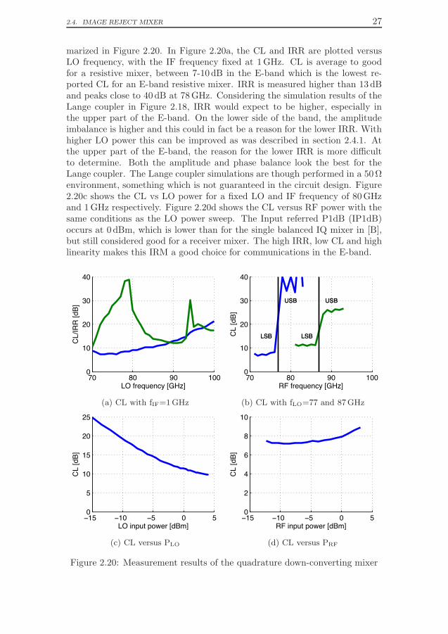
marized in Figure 2.20. In Figure 2.20a, the CL and IRR are plotted versusLO frequency, with the IF frequency fixed at 1GHz. CL is average to goodfor a resistive mixer, between 7-10dB in the E-band which is the lowest re-ported CL for an E-band resistive mixer. IRR is measured higher than 13 dBand peaks close to 40 dB at 78GHz. Considering the simulation results of theLange coupler in Figure 2.18, IRR would expect to be higher, especially inthe upper part of the E-band. On the lower side of the band, the amplitudeimbalance is higher and this could in fact be a reason for the lower IRR. Withhigher LO power this can be improved as was described in section 2.4.1. Atthe upper part of the E-band, the reason for the lower IRR is more di!cultto determine. Both the amplitude and phase balance look the best for theLange coupler. The Lange coupler simulations are though performed in a 50#environment, something which is not guaranteed in the circuit design. Figure2.20c shows the CL vs LO power for a fixed LO and IF frequency of 80GHzand 1GHz respectively. Figure 2.20d shows the CL versus RF power with thesame conditions as the LO power sweep. The Input referred P1dB (IP1dB)occurs at 0 dBm, which is lower than for the single balanced IQ mixer in [B],but still considered good for a receiver mixer. The high IRR, low CL and highlinearity makes this IRM a good choice for communications in the E-band.
70 80 90 1000
10
20
30
40
LO frequency [GHz]
CL/IR
R [d
B]
(a) CL with fIF=1GHz
70 80 90 1000
10
20
30
40
USB USB
LSB LSB
USB USB
LSB LSB
RF frequency [GHz]
CL [d
B]
(b) CL with fLO=77 and 87GHz
−15 −10 −5 0 50
5
10
15
20
25
LO input power [dBm]
CL [d
B]
(c) CL versus PLO
−15 −10 −5 0 50
2
4
6
8
10
RF input power [dBm]
CL [d
B]
(d) CL versus PRF
Figure 2.20: Measurement results of the quadrature down-converting mixer

28 CHAPTER 2. MIXERS FOR E-BAND COMMUNICATIONS
Chapter 3
53 GHz single chip receiver
Weather conditions have always been of interest to the human being. In thenordic countries the prediction and accuracy of the weather forecasts has al-ways been a subject of discussion. Apart from the common interest from thepublic, many businesses rely on accurate weather services and are willing topay for more predictable now casting services. Long term climate e"ects aregenerally not covered from this application.
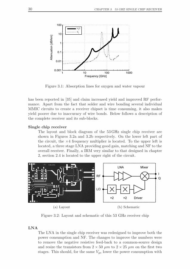
Meteorologists now look for alternative solutions to achieve more accu-rate short term weather predictions. Future mm and sub-mm radiometersfor remote sensing in GEO are studied and compared with Low Earth Orbit(LEO) [33]. The primary advantage with GEO is its continuous coverage ofa large area of the earth’s atmosphere. Moreover, temperature and humid-ity profiles with high horizontal resolution under all weather conditions makethis solution very attractive for nowcasting service. Especially interesting arefrequencies close to the water vapour and oxygen absorption lines at 60, 118,183 and 380GHz. In Figure 3.1, the attenuation levels for oxygen and watervapour are separatly plotted from the overall atmosphere attenuation withclear resonances at the mentioned frequency points. With the advances madein semiconductor technologies it’s possible to make such radiometer systemsfor mm-wave and sub-mm wave with MMIC solutions.
In 2007, a Geostationary Atmospheric Sounder (GAS) demonstrator wasbuilt with 20 elements of 53GHz receiver chips. When built, the completeGAS will consist of 136 elements of 53GHz receivers, 107 elements of 118,183 and 380GHz with a total power consumption and mass budget of 300Wand 300 kg respectively [6]. For the demonstrator, a 53GHz single chip MMICwas developed from Chalmers [34], but power consumption and IQ balanceespecially needed to be improved to fulfill the requirements. For this reason,this second generation single chip 53GHz receiver chip with a new LNA, !4frequency multiplier and IRM was designed to improve power consumption,IRR and NF.
3.1 Design
The receiver chip consists of a !4 frequency multiplier, an IQ mixer and anLNA integrated on the chip. Integration of mixed functions into a single chip
29
30 CHAPTER 3. 53 GHZ SINGLE CHIP RECEIVER
1 10 100 10000.001
0.01
0.1
1
10
100
Frequency [GHz]
Atte
nuat
ion
[dB/
km]
H
2O
O2
Figure 3.1: Absorption lines for oxygen and water vapour
has been reported in [35] and claim increased yield and improved RF perfor-mance. Apart from the fact that solder and wire bonding several individualMMIC circuits to create a receiver chipset is time consuming, it also makesyield poorer due to inaccuracy of wire bonds. Below follows a description ofthe complete receiver and its sub-blocks.
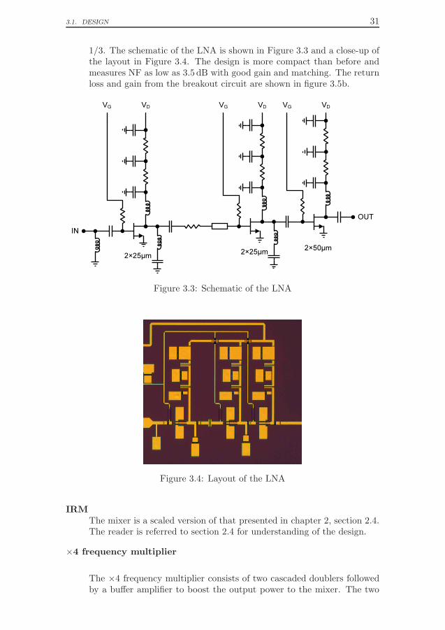
Single chip receiverThe layout and block diagram of the 53GHz single chip receiver areshown in Figures 3.2a and 3.2b respectively. On the lower left part ofthe circuit, the !4 frequency multiplier is located. To the upper left islocated, a three stage LNA providing good gain, matching and NF to theoverall receiver. Finally, a IRM very similar to that designed in chapter2, section 2.4 is located to the upper right of the circuit.
(a) Layout
I
Q
RF
LO
LNA
!2 !2 Driver
Mixer
(b) Schematic
Figure 3.2: Layout and schematic of this 53 GHz receiver chip
LNAThe LNA in the single chip receiver was redesigned to improve both thepower consumption and NF. The changes to improve the numbers wereto remove the negative resistive feed-back to a common-source designand resize the transistors from 2! 50 µm to 2! 25 µm on the first twostages. This should, for the same Vgs lower the power consumption with
3.1. DESIGN 31
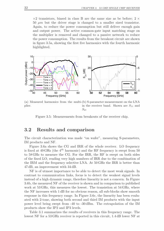
1/3. The schematic of the LNA is shown in Figure 3.3 and a close-up ofthe layout in Figure 3.4. The design is more compact than before andmeasures NF as low as 3.5 dB with good gain and matching. The returnloss and gain from the breakout circuit are shown in figure 3.5b.
2!25"m
IN
VD
VG
2!25"m
VD
VG
2!50"m
OUT
VD
VG
Figure 3.3: Schematic of the LNA
Figure 3.4: Layout of the LNA
IRM
The mixer is a scaled version of that presented in chapter 2, section 2.4.The reader is referred to section 2.4 for understanding of the design.
!4 frequency multiplier
The !4 frequency multiplier consists of two cascaded doublers followedby a bu"er amplifier to boost the output power to the mixer. The two
32 CHAPTER 3. 53 GHZ SINGLE CHIP RECEIVER
!2 transistors, biased in class B are the same size as be before; 2 !50 µm but the driver stage is changed to a smaller sized transistor.Again, to reduce the power consumption but still deliver enough gainand output power. The active common-gate input matching stage onthe multiplier is removed and changed to a passive network to reducethe power consumption. The results from the breakout circuit are shownin figure 3.5a, showing the first five harmonics with the fourth harmonichighlighted.
40 45 50 55 60−50
−40
−30
−20
−10
0
10
Frequency [GHz]
Out
put p
ower
[dBm
]
Tone = 1Tone = 2Tone = 3Tone = 4Tone = 5
(a) Measured harmonics from the multi-plier.
50 52 54 56 58 600
10
20
30
S 21 [d
B]
Frequency [GHz]
50 52 54 56 58 60−15
−10
−5
0
S21S11
(b) S-parameter measurement on the LNAin the receiver band. Shown are S11 andS21
Figure 3.5: Measurements from breakouts of the receiver chip.
3.2 Results and comparison
The circuit characterization was made “on wafer”, measuring S-parameters,IM products and NF.
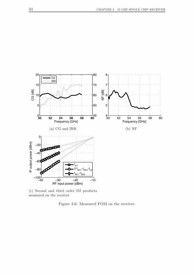
Figure 3.6a shows the CG and IRR of the whole receiver. LO frequencyis fixed at 49GHz (the 4th harmonic) and the RF frequency is swept from 50to 58GHz to measure the CG. For the IRR, the RF is swept on both sidesof the fixed LO, reading very high numbers of IRR due to the combination ofthe IRM and the frequency selective LNA. At 50GHz the IRR is better than47dB, an improvement with 34 dB.
NF is of utmost importance to be able to detect the most weak signals. Incontrast to communication links, focus is to detect the weakest signal levelsinstead of a high dynamic range, therefore linearity is not a concern. In Figure3.6b, the measured NF of the receiver is shown and in comparison to publishedwork at 53GHz, this measures the lowest. The transistion at 54GHz, wherethe NF increases with 1 dB for no obvious reason, all sub-blocks show smoothresponse in this frequency range. In Figure 3.6c, the linearity has been evalu-ated with 2-tone, showing both second and third IM products with the inputpower level being swept from -40 to -30dBm. The extrapolation of the IMproducts show the IP2 and IP3 levels.
Table 3.1 summarizes the results of receivers in this frequency range. Thelowest NF for a 53GHz receiver is reported in this circuit, 1.4 dB lower NF at
3.2. RESULTS AND COMPARISON 33
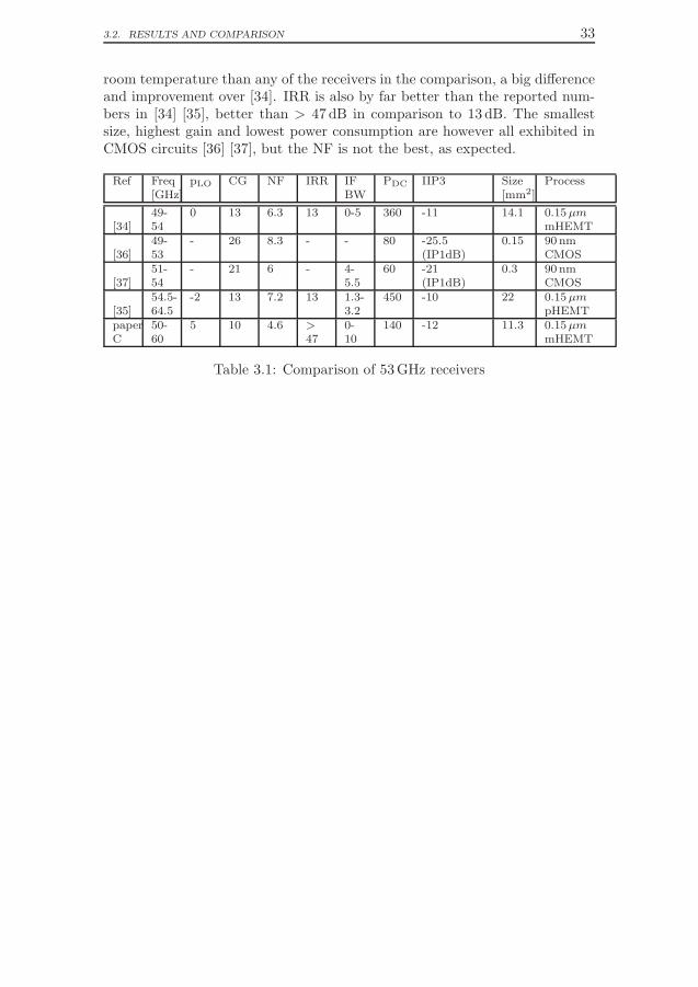
room temperature than any of the receivers in the comparison, a big di"erenceand improvement over [34]. IRR is also by far better than the reported num-bers in [34] [35], better than > 47 dB in comparison to 13 dB. The smallestsize, highest gain and lowest power consumption are however all exhibited inCMOS circuits [36] [37], but the NF is not the best, as expected.
Ref Freq[GHz]
pLO CG NF IRR IFBW
PDC IIP3 Size[mm2]
Process
[34]49-54
0 13 6.3 13 0-5 360 -11 14.1 0.15µmmHEMT
[36]49-53
- 26 8.3 - - 80 -25.5(IP1dB)
0.15 90 nmCMOS
[37]51-54
- 21 6 - 4-5.5
60 -21(IP1dB)
0.3 90 nmCMOS
[35]54.5-64.5
-2 13 7.2 13 1.3-3.2
450 -10 22 0.15µmpHEMT
paperC
50-60
5 10 4.6 >
470-10
140 -12 11.3 0.15µmmHEMT
Table 3.1: Comparison of 53GHz receivers
34 CHAPTER 3. 53 GHZ SINGLE CHIP RECEIVER
50 52 54 56 58 600
5
10
15
20
Frequency [GHz]
CG [d
B]
50 52 54 56 58 6040
50
60
70
80
IRR
[dB]
CGIRR
(a) CG and IRR
50 52 54 56 58 604
5
6
7
8
Frequency [GHz]
NF [d
B]
(b) NF
−40 −30 −20 −10−100
−80
−60
−40
−20
0
RF input power [dBm]
IF o
utpu
t pow
er [d
Bm]
fIF12*fRF1−fRF2−fLOfRF1−fRF2
(c) Second and third order IM productsmeasured on the receiver
Figure 3.6: Measured FOM on the receiver.
Chapter 4
Conclusions
Two resistive quadrature MMIC mixers have been designed in a 0.15µmmHEMT technology for wideband communications at E-band, most commonlyreferred to 71-76 and 81-86GHz. The two mixers show excellent performanceover wide RF and IF bandwidths and state-of-the-art OIP3 for a resistivemixer. A novel di"erential branchline coupler was used in the design in pa-per B to add LO-RF isolation to the circuit while minimizing size and addingfunctionality. The increase in size was only 25% in comparison to the circuitin paper A, a similar circuit without this function. In addition to added func-tionality, the properties of DM and CM signals were shown to be beneficialfor further improving the balance. DM signals are often used in CMOS andBiCMOS due to the lossy substrate but they are not commonly used in GaAsHEMT. The results and implementation of the design in paper B with di"er-ential signals showed improved performance and small size. The broadband,smooth CL, high IRR and high linearity makes both IQ modulators very wellsuited for E-band RF-frontends.
A 53GHz single chip receiver for atmospheric remote sensing in GEO wasdesigned, fabricated and characterized. Its performance show state-of-the-artNF, 1.4 dB lower than any published 53GHz receiver. The power saving design,low NF and high IRR make this single chip receiver suited for atmosphericremote sensing.
35
36 CHAPTER 4. CONCLUSIONS
4.1 Future work
Wideband communication in the mm- and sub-mm wave (220 and 340GHz)are interesting frequency windows for high data rate communication due totheir vast available bandwidths and relatively low atmospheric attenuation.The high carrier frequency makes the relative RF bandwidth smaller to ef-fectively support larger data bandwidths. Data bandwidths up to or beyond30GHz can possibly reach 100Gbps with fairly simple modulation. Emergingtechnologies, such as SiGe and InP HBT support medium-, large- and verylarge scale integration levels with high fT /fmax to allow complete integrationwith RF front-ends together with back-end digital circuits to be designed ona single chip. Integration of more circuit blocks on chip, especially basebandcircuits are intriguing ideas to try for increasing wireless transmission datarates.
Acknowledgment
I cannot conclude this work without thanking the people that made this pos-sible.
A very special thank you I want to express to my examiner and supervisorProf. Herbert Zirath. He welcomed me to Microwave Electronics Laboratory(MEL) already in 2004 to do my master’s thesis. Later, in 2007 he gave me theopportunity to come back to Chalmers to participate in a project for marketrelated research on high frequency circuit design together with the possibilityof starting a company based on the research carried out at MEL. In 2009 camethe opportunity to combine this work with the research at MEL in order topursue a Ph.D., a possibility I’m very grateful for. His expertise of circuitdesign and cross disciplinary knowledge has been the base and inspiration ofthis work.
I wish to thank my co-supervisor Sten Gunnarsson for taking part in mywork with discussions and guidance. He introduced me to the field of mi-crowave circuits, an area I enjoy very much working with.
I would like to thank my co-supervisorMattias Ferndahl for all the technicaldiscussions and unconditional assistance in the lab.
A special thanks goes to Trajan Badju for supporting the research workbeing pursued at MEL and for being an excellent boss and friend.
A thank you is also directed to Iltcho Angelov for broadening the contextof this work and his enthusiasm to teach me about device modeling and otherrelated topics.
I want to acknowledge Bertil Hansson for making, always with enthusiasm,great design-kits to work with.
I also want to thank my colleagues and friends; Zhongxia (Simon), Oliver,Olle, Cesar, Morteza and all the people at MEL and Gotmic for making themgreat places to work at.
I express my deepest gratitude to Helena, my family and friends for all thesupport and love I get from them.
Finally, I would like to acknowledge the financing institutions and collabo-ration partners which made this work possible. This work has been supportedby “Vinn Verifiering” which is funded by Swedish Governmental Agency of In-novation Systems (VINNOVA) and “System on chip solutions for future highspeed communication” which is funded by Swedish Foundation for StrategicReasearch (SSF). Gotmic for supporting and funding tapeouts and publishingacademic material. WIN semiconductors is acknowledged for processing thecircuits.
37

Bibliography
[1] W. R. Deal, K. Leong, V. Radisic, S. Sarkozy, B. Gorospe, J. Lee, P. H.Liu, W. Yoshida, J. Zhou, M. Lange, R. Lai, and X. B. Mei, “Low NoiseAmplification at 0.67 THz Using 30 nm InP HEMTs,” Microwave andWireless Components Letters, IEEE, vol. 21, no. 7, pp. 368–370, 2011.
[2] A. Fehske, G. Fettweis, J. Malmodin, and G. Biczok, “The global footprintof mobile communications: The ecological and economic perspective,”Communications Magazine, IEEE, vol. 49, no. 8, pp. 55–62, 2011.
[3] “Cisco Visual Networking Index (VNI): Global Mobile Data Tra!c Fore-cast Update, 2012-2017,” 2012.
[4] “Radio-frequency arrangements for fixed service systems,” 2012-03 2012.
[5] J. Wells, “Faster than fiber: The future of multi-G/s wireless,”MicrowaveMagazine, IEEE, vol. 10, no. 3, pp. 104–112, 2009.
[6] J. Christensen, A. Carlstrom, H. Ekstrom, A. Emrich, J. Embretsen,P. De Maagt, and A. Colliander, “GAS: the Geostationary AtmosphericSounder,” in Geoscience and Remote Sensing Symposium, 2007. IGARSS2007. IEEE International, pp. 223–226.
[7] M. Willis, “Propagation tutorial,” 2007. [Online]. Available:http://www.mike-willis.com/Tutorial/PF5.htm
[8] S. Voinigescu, High-Frequency Integrated Circuits. The Cambridge RFand Microwave Engineering Series, 2013.
[9] C. Jingjing, H. Zhongxia, B. Lei, C. Svensson, L. Yinggang, S. Gunnars-son, C. Stoij, and H. Zirath, “10 Gbps 16QAM transmission over a 70/80GHz (E-band) radio test-bed,” in Microwave Integrated Circuits Confer-ence (EuMIC), 2012 7th European, pp. 556–559.
[10] A. Hirata, T. Kosugi, H. Takahashi, R. Yamaguchi, F. Nakajima, T. Fu-ruta, H. Ito, H. Sugahara, Y. Sato, and T. Nagatsuma, “120-GHz-bandmillimeter-wave photonic wireless link for 10-Gb/s data transmission,”Microwave Theory and Techniques, IEEE Transactions on, vol. 54, no. 5,pp. 1937–1944, 2006.
[11] J. Antes, D. Lopez-Diaz, U. J. Lewark, S. Wagner, A. Tessmann,A. Leuther, and I. Kallfass, “A high linearity I/Q mixer for high datarate E-band wireless communication links,” in Microwave Integrated Cir-cuits Conference (EuMIC), 2012 7th European, pp. 278–281.
39
40 BIBLIOGRAPHY
[12] B. Gilbert, “A precise four-quadrant multiplier with subnanosecond re-sponse,” Solid-State Circuits, IEEE Journal of, vol. 3, no. 4, pp. 365–373,1968.
[13] L. A. NacEachern and T. Manku, “A charge-injection method for Gilbertcell biasing,” in Electrical and Computer Engineering, 1998. IEEE Cana-dian Conference on, vol. 1, pp. 365–368 vol.1.
[14] O. Mitrea, C. Popa, A. M. Manolescu, and M. Glesner, “A linearizationtechnique for radio frequency CMOS Gilbert-type mixers,” in Electronics,Circuits and Systems, 2003. ICECS 2003. Proceedings of the 2003 10thIEEE International Conference on, vol. 3, pp. 1086–1089 Vol.3.
[15] B. Gilbert, “The MICROMIXER: a highly linear variant of the Gilbertmixer using a bisymmetric Class-AB input stage,” Solid-State Circuits,IEEE Journal of, vol. 32, no. 9, pp. 1412–1423, 1997.
[16] W. Li, R. Kraemer, and J. Borngraeber, “An Improved Highly-LinearLow-Power Down-Conversion Micromixer for 77 GHz Automotive Radarin SiGe Technology,” inMicrowave Symposium Digest, 2006. IEEE MTT-S International, pp. 1834–1837.
[17] S. A. Maas, “A GaAs MESFET Mixer with Very Low Intermodulation,”Microwave Theory and Techniques, IEEE Transactions on, vol. 35, no. 4,pp. 425–429, 1987.
[18] S. A. Maas, Microwave Mixers, Second Edition. Norwood, MA: ArtechHouse, 1992.
[19] M. Varonen, M. Karkkainen, J. Riska, P. Kangaslahti, and K. A. I. Halo-nen, “Resistive HEMT mixers for 60-GHz broad-band telecommunica-tion,” Microwave Theory and Techniques, IEEE Transactions on, vol. 53,no. 4, pp. 1322–1330, 2005.
[20] K. Sung-Chan, A. Dan, L. Byeong-Ok, T. J. Baek, S. Dong-Hoon, andR. Jin-Koo, “High-performance 94-GHz single balanced mixer using 70-nm MHEMTs and surface micromachined technology,” Electron DeviceLetters, IEEE, vol. 27, no. 1, pp. 28–30, 2006.
[21] C. Wagner, M. Hartmann, A. Stelzer, and H. Jaeger, “A Fully Di"eren-tial 77-GHz Active IQ Modulator in a Silicon-Germanium Technology,”Microwave and Wireless Components Letters, IEEE, vol. 18, no. 5, pp.362–364, 2008.
[22] T. N. Ton, T. H. Chen, K. W. Chang, H. Wang, T. L. Tan, G. S. Dow,G. M. Hayashibara, B. Allen, and J. Berenz, “A W-band monolithic In-GaAs/GaAs HEMT Schottky diode image reject mixer,” in Gallium Ar-senide Integrated Circuit (GaAs IC) Symposium, 1992. Technical Digest1992., 14th Annual IEEE, pp. 63–66.
[23] Y. Hamada, K. Maruhashi, M. Ito, S. Kishimoto, T. Morimoto, andK. Ohata, “A 60-GHz-band Compact IQ Modulator MMIC for Ultra-high-speed Wireless Communication,” in Microwave Symposium Digest,2006. IEEE MTT-S International, pp. 1701–1704.
BIBLIOGRAPHY 41
[24] C. Hong-Yeh, H. Tian-Wei, W. Huei, W. Yu-Chi, C. Pane-Chane, andC. Chung-Hsu, “Broad-band HBT BPSK and IQ modulator MMICsand millimeter-wave vector signal characterization,” Microwave Theoryand Techniques, IEEE Transactions on microwave theory and techniques,vol. 52, no. 3, pp. 908–919, 2004.
[25] T. Jeng-Han, W. Pei-Si, L. Chin-Shen, H. Tian-Wei, J. G. J. Chern, andH. Wen-Chu, “A 25-75 GHz Broadband Gilbert-Cell Mixer Using 90-nmCMOS Technology,”Microwave and Wireless Components Letters, IEEE,vol. 17, no. 4, pp. 247–249, 2007.
[26] T. Mimura, S. Hiyamizu, T. Fujii, and K. Nanbu, “A New Field-E"ect Transistor with Selectively Doped GaAs/n-AlxGa1"xAs Hetero-junctions,” Japanese Journal of Applied Physics, vol. 19, no. 5, pp. 225–227, 1980.
[27] M. Abbasi, T. Kjellberg, S. E. Gunnarsson, and H. Zirath, “Direct carrierquadrature modulator and Demodulator MMICs for 60 GHz gigabit wire-less communications,” in Microwave Conference Proceedings (APMC),2011 Asia-Pacific, pp. 1134–1137.
[28] Agilent Technologies, “Circuit components: nonlinear devices,” pp. 261–308, 2008.
[29] E. J. G. Matthaei, L. Young, Microwave Filters, Impedance-MatchingNetworks and Coupling Structures. Artech House, 1980.
[30] D. E. Bockelman and W. R. Eisenstadt, “Combined di"erential andcommon-mode scattering parameters: theory and simulation,” MicrowaveTheory and Techniques, IEEE Transactions on, vol. 43, no. 7, pp. 1530–1539, 1995.
[31] N. Marchand, “Transmission-Line Conversion transformers,” Electronics,vol. 17, no. December, pp. 142–145, 1944.
[32] L. Rui and K. Dong Il, “A new compact low-pass filter with broad stop-band and sharp skirt characteristics,” in Microwave Conference Proceed-ings, 2005. APMC 2005. Asia-Pacific Conference Proceedings, vol. 3, p.3 pp.
[33] U. Klein, L. Chung-Chi, N. Atkinson, J. Charlton, and C. Philpot, “Fu-ture microwave radiometers in geostationary and medium earth orbit,”in Geoscience and Remote Sensing Symposium, 2003. IGARSS ’03. Pro-ceedings. 2003 IEEE International, vol. 3, pp. 2158–2160.
[34] S. E. Gunnarsson, A. Emrich, H. Zirath, R. Kozhuharov, C. Karnfelt,J. Embretsen, and C. Tegnander, “A single-chip 53 GHz radiometer front-end MMIC for geostationary atmospheric measurements,” in Radio andWireless Symposium, 2008 IEEE, pp. 867–870.
[35] S. E. Gunnarsson, C. Karnfelt, H. Zirath, R. Kozhuharov, D. Kuylen-stierna, A. Alping, and C. Fager, “Highly integrated 60 GHz transmitterand receiver MMICs in a GaAs pHEMT technology,” Solid-State Circuits,IEEE Journal of, vol. 40, no. 11, pp. 2174–2186, 2005.

42 BIBLIOGRAPHY
[36] B. Razavi, “A Millimeter-Wave CMOS Heterodyne Receiver With On-Chip LO and Divider,” Solid-State Circuits, IEEE Journal of, vol. 43,no. 2, pp. 477–485, 2008.
[37] D. Alldred, B. Cousins, and S. P. Voinigescu, “A 1.2V, 60-GHz radio re-ceiver with on-chip transformers and inductors in 90-nm CMOS,” in Com-pound Semiconductor Integrated Circuit Symposium, 2006. CSIC 2006.IEEE, pp. 51–54.

Paper A
An Image Reject Mixer for High-Speed E-band (71-76,81-86 GHz) Wireless Communication
Marcus Gavell, Mattias Ferndahl, Sten E. Gunnarsson, Morteza Ab-basi, Herbert Zirath


Paper B
A linear 70-95 GHz di!erential IQ modulator for E-bandWireless Communication
Marcus Gavell, Herbert Zirath, Mattias Ferndahl, Sten E. Gunnars-son

Paper C
A 53 GHz single chip Receiver for Geostationary Atmo-spheric Measurements
Marcus Gavell, Mattias Ferndahl, Sten E. Gunnarsson, Herbert Zi-rath